Introdução à Micro-Informática - PUC-Riomicro/SLIDES/Internal Memory.pdf · Flash memory...
31
Internal Memory Patrick Happ Raul Queiroz Feitosa
Transcript of Introdução à Micro-Informática - PUC-Riomicro/SLIDES/Internal Memory.pdf · Flash memory...

Internal Memory
Patrick Happ
Raul Queiroz Feitosa
Internal Memory 2
Objective
To present a survey of semiconductor main
memory technology.
Internal Memory 3
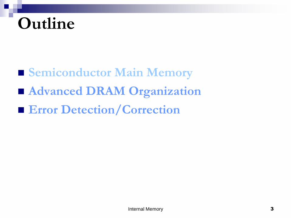
Outline
Semiconductor Main Memory
Advanced DRAM Organization
Error Detection/Correction

Internal Memory 4 01/09/2017
Semiconductor Memory Types
Memory Type Category Erasure Write Mechanism Volatility
Random-access
memory (RAM)
Read-write
memory
Electrically, byte-
level Electrically Volatile
Read-only
memory (ROM) Read-only
memory Not possible
Masks
Nonvolatile
Programmable
ROM (PROM)
Electrically
Erasable PROM
(EPROM)
Read-mostly
memory
UV light, chip-
level
(EEPROM) Electrically, byte-
level
Flash memory Electrically, block-
level

Internal Memory 5 01/09/2017
Semiconductor Memory Types
RAM
ROM
PROM
EPROM EEPROM
E2PROM
FLASH

Internal Memory 6 01/09/2017
Memory Cell Operation
Internal Memory 7 01/09/2017
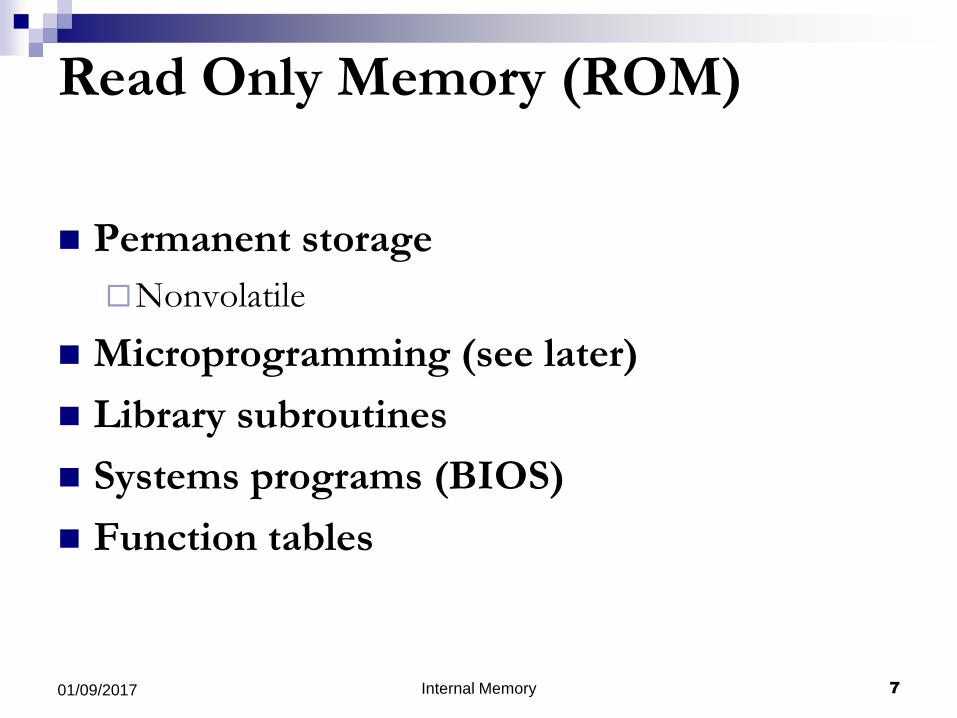
Read Only Memory (ROM)
Permanent storage
Nonvolatile
Microprogramming (see later)
Library subroutines
Systems programs (BIOS)
Function tables

Internal Memory 8 01/09/2017
Types of ROM
Written during manufacture
Very expensive for small runs
Programmable (once)
PROM
Needs special equipment to program
Read “mostly”
Erasable Programmable (EPROM)
Erased by UV
Electrically Erasable (EEPROM)
Takes much longer to write than read
Flash memory
Erase whole memory electrically
Internal Memory 9 01/09/2017
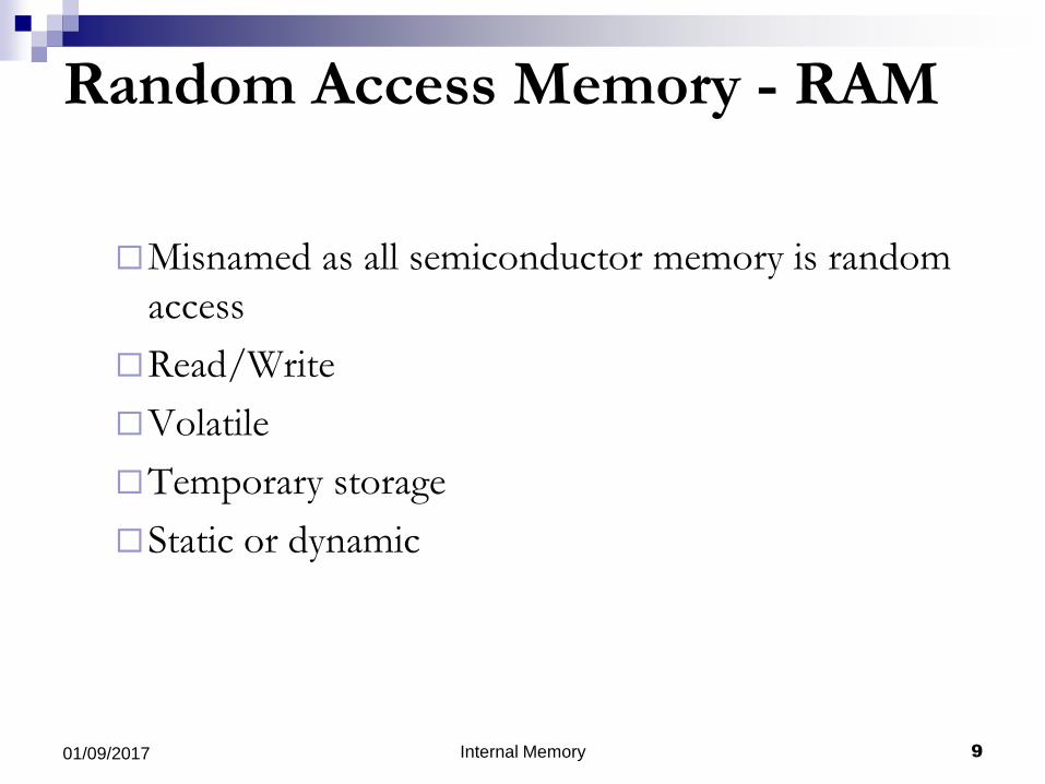
Random Access Memory - RAM
Misnamed as all semiconductor memory is random
access
Read/Write
Volatile
Temporary storage
Static or dynamic
Internal Memory 10 01/09/2017
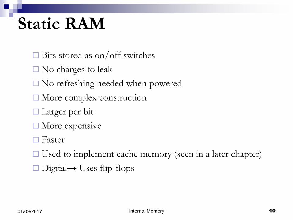
Static RAM
Bits stored as on/off switches
No charges to leak
No refreshing needed when powered
More complex construction
Larger per bit
More expensive
Faster
Used to implement cache memory (seen in a later chapter)
Digital→ Uses flip-flops

Internal Memory 11 01/09/2017
Static RAM Structure
high low
off
off
on
on
state 1 state 1
low high
on
on
off
off
state 0
Read
value is on line B Write applies
value to B and
compliment to B
Internal Memory 12 01/09/2017
Dynamic RAM
Bits stored as charge in capacitors
Charges leak
Need refreshing even when powered
Simpler construction
Smaller per bit
Less expensive
Need refresh circuits
Slower
Used to implement main memory
Essentially analogue → Level of charge determines value

Internal Memory 13 01/09/2017
Dynamic RAM Structure
0/1 on
charge
transfered
to capacitor
Write
0/1 on
charge fed
through
line to
sensor
Read
Internal Memory 14 01/09/2017
Refreshing
Refresh circuit included on chip
Disable chip
Count through rows
Read & Write back
Takes time
Slows down apparent performance

Internal Memory 15 01/09/2017
SRAM DRAM
Both volatile
Power needed to preserve data
Dynamic cell
Simpler to build, smaller
More dense
Less expensive
Needs refresh
Larger memory units
Static
Faster
Cache

Internal Memory 16 01/09/2017
Simplified DRAM Read Timing
Internal Memory 17 01/09/2017
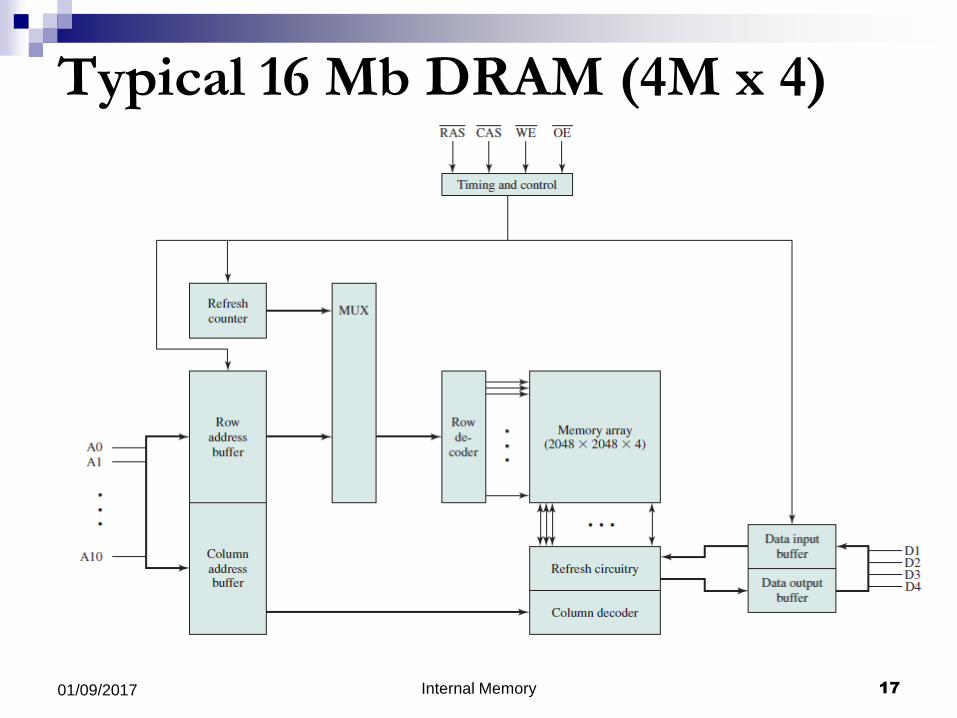
Typical 16 Mb DRAM (4M x 4)
Internal Memory 18 01/09/2017
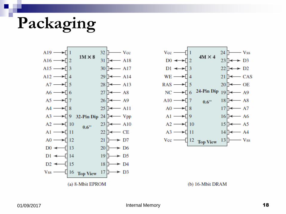
Packaging
Internal Memory 19
Outline
Semiconductor Main Memory
Advanced DRAM Organization
Error Detection/Correction

Internal Memory 20 01/09/2017
Advanced DRAM Organization
Basic DRAM same since 70’s.
Enhanced DRAM
Contains small SRAM as well
SRAM holds last line read (c.f. Cache!)
Internal Memory 21 01/09/2017
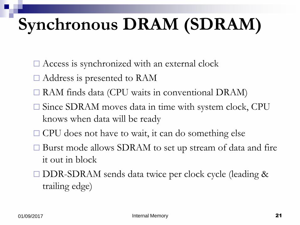
Synchronous DRAM (SDRAM)
Access is synchronized with an external clock
Address is presented to RAM
RAM finds data (CPU waits in conventional DRAM)
Since SDRAM moves data in time with system clock, CPU
knows when data will be ready
CPU does not have to wait, it can do something else
Burst mode allows SDRAM to set up stream of data and fire
it out in block
DDR-SDRAM sends data twice per clock cycle (leading &
trailing edge)

Internal Memory 22 01/09/2017
SDRAM Read Timing
valid
data
valid
data valid
data
valid
data
Internal Memory 23 01/09/2017
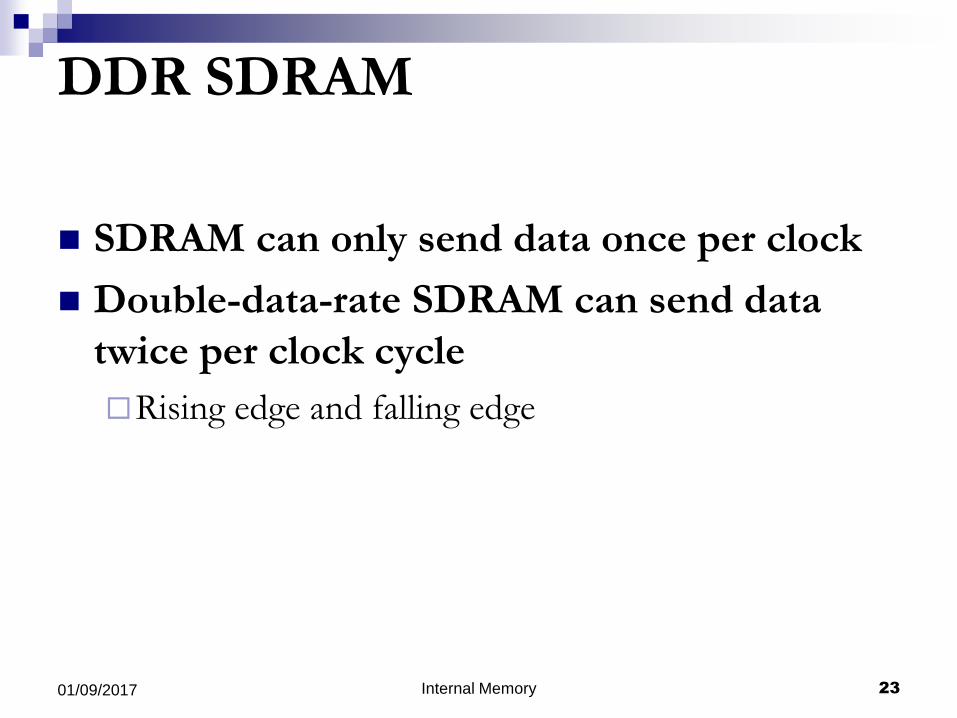
DDR SDRAM
SDRAM can only send data once per clock
Double-data-rate SDRAM can send data
twice per clock cycle
Rising edge and falling edge

Internal Memory 24 01/09/2017
DDR SDRAM - Read Timing

DDR Generations
By increasing the operational frequency and
the prefetch buffer from 2 to 4 and to 8 bits
higher data rates were achieved
Internal Memory 25 01/09/2017
DDR
SDRAM
Standard
Bus clock
(MHz)
Internal rate
(MHz)
Prefetch
(min burst)
Transfer Rate
(MT/s)
First
release
DDR 100–200 100–200 2n 200–400 2000
DDR2 200–533.33 100–266.67 4n 400–1066.67 2004
DDR3 400–1066.67 100–266.67 8n 800–2133.33 2007
DDR4 1066.67–2133.33 133.33–266.67 8n 2133.33–4266.67 2011
DDR5 Specifications expected to be released by 2017 2020
Internal Memory 26
Outline
Semiconductor Main Memory
Advanced DRAM Organization
Error Detection/Correction

Internal Memory 27 01/09/2017
Error Correction
Hard Failure
Permanent defect
Soft Error
Random, non-destructive
No permanent damage to memory
Detected using Hamming error correcting
code
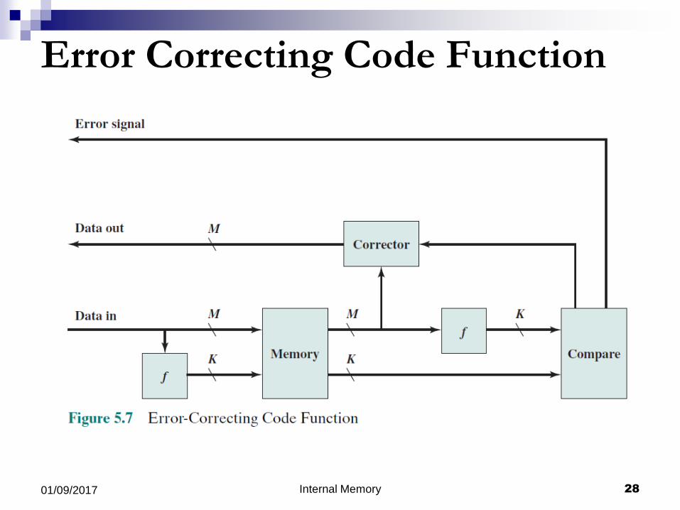
Internal Memory 28 01/09/2017
Error Correcting Code Function

Review Material
The Review Questions and Problems at the end of
chapter 5 of Stalling’s book are strongly
recommended.
Internal Memory 29 01/09/2017
Internal Memory 30 01/09/2017
Text Book References
The topics are covered in
Tanenbaum -
Stallings - chapter 5.
Parhami -

Internal Memory 31 01/09/2017
Internal Memory
END