Introduction · Web viewBandwidth. Word transmission rate. Latency. Time to access the first of a...
26
The Memory Hierarchy Introduction Terminology Access time Time to access a word in memory Specifies the read or write time Note these may be different The memory may be organized as Bits, bytes, or words Cycle time Time from the start of one read until the next Block size Number of words in a block Note this is a logical description Bandwidth Word transmission rate Latency Time to access the first of a sequence of words Block access time Time to access an entire block from the start of a read DRAM Dynamic random access memory SRAM Static random access memory Semi-static RAM The periphery is clock activated (dynamic) - thus is inactive until clocked. Only one memory cycle is permitted per clock Periphery circuitry must be allowed to reset after each active memory cycle for min precharge time. No refresh is required. SDRAM Synchronous DRAM SDRAM synchronizes all addresses, data, and control signals to the system clock. Allows much higher data transfer rates that asynchronous transfers ROM Read only memory PROM
Transcript of Introduction · Web viewBandwidth. Word transmission rate. Latency. Time to access the first of a...

The Memory HierarchyIntroduction
TerminologyAccess time
Time to access a word in memorySpecifies the read or write time
Note these may be differentThe memory may be organized as
Bits, bytes, or wordsCycle time
Time from the start of one read until the nextBlock size
Number of words in a blockNote this is a logical description
BandwidthWord transmission rate
LatencyTime to access the first of a sequence of words
Block access timeTime to access an entire block from the start of a read
DRAMDynamic random access memory
SRAMStatic random access memory
Semi-static RAMThe periphery is clock activated (dynamic) - thus is inactive until clocked.Only one memory cycle is permitted per clockPeriphery circuitry must be allowed to reset after each active memory cycle for min precharge time.No refresh is required.
SDRAMSynchronous DRAM SDRAM synchronizes all addresses, data, and control signals to the system clock. Allows much higher data transfer rates that asynchronous transfers
ROMRead only memory
PROMProgrammable read only memory
EPROMErasable programmable read only memory
EEPROMElectrically erasable programmable read only memory
CASColumn address strobeClock in used in dynamic memories to control the input of column addresses
RAS

Row address strobeClock in used in dynamic memories to control the input of row addresses
RefreshTechnique used in dram or SDRAM through which data is retained in memory
Refresh time intervalTime between two refresh operations - determine by system in which memory is operating
Memory block on Von Neumann machinesActually comprised of number of memory components
Arranged In hierarchical mannerTo co-operate with each other
Hierarchical metricsSpeedStorage capacity
At topSlowest largest memories
Also known as secondary memoryAlso tend to be least expensiveSize
On order of 10’s to 100’s of gigabitsLatency
On the order of 10’s of msBandwidth
1 MB per secCost
$0.02 per MBDevices
Tape for archival storageHigh density disk drives
BottomSmallest fastest memories
Call this cache memoryAlso tend to be most expensiveSize
On order of 100’s to 1000’s bitsUp to several M in some machines today
Latency 10-20 ns
Bandwidth8-10 MB per sec
Cost per MB$500.00
Devices

RegistersHigh speed cache
MiddleOften called primary memorySize
On order of 100’s of M bits to 1’s of G bitsLatency
50 nsBandwidth
1 MB per secCost
$30.00 per MBDevices
RAM ROMSome hard drivesLower speed cache
MotivationWe would prefer program to execute as quickly as possibleAs we’ve seen
Accessing memory takes timeEach access contributes to time required to execute instruction
Static Ram Design
A typical SRAM cell appears as follows
Observe that we have 6 transistors per cell

Two access transistors enable the cell forRead and write
Write operationValue written into cell by
Applying value to bi and !bI through write / sense amplifiers Assert word line Causes new value to be written into latch
Read operationValue read from cell by
Precharge bi and !bi to voltage halfway between 0 and 1 Assert the word line Drives bi and !bi to high and low or low and high Values are sensed and amplified by write / sense amplifier
Typical timing is given as
DRAM DesignA typical DRAM cell appears as follows

Observe that we have only one transistor per cellRead and write operations use single bit line
Write operationValue written into cell by
Applying 0 or 1 to bi through write / sense amplifiers Assert word line Charges cap if 1 stored discharges if 0 stored
Read operationValue read from cell by
Precharge bi to voltage halfway between 0 and 1 Assert the word line Gates signal onto bi
Values are sensed and amplified by write / sense amplifier Read operation causes cap to discharge Sensed and amplified value placed back on bit line
Called a refresh operation
Typical timing is given as shown

Chip OrganizationIndependent of type of internal storageTypical RAM chip configured as shown in following drawing
Making Things WorkLocality of Reference
Goal Reduce number of accessesMake each access short as possibleUtilized to much greater extent in today’s memories
Ideally would like to make all memory as fast as technology allowsSuch action has associated cost
Memories near bottom are expensiveSupport circuitry for such memories also expensive
Additional circuitry requiredPower supplies to support
Almost all programs executed today written using procedural paradigmIf we analyze how such programs
DesignedExecute
Discover interesting phenomenonExecution generally occurs
SequentiallySmall loops
Number of instructions
Means overall progress forward through program

Executing at much lower rate than Access times of fastest memory
Put another wayWith respect to entire program
We are executing within a small windowThat moves forward through programThis is shown as the following
Formally such phenomenon calledLocality of referenceWe recognize program executing only few instructions
Within small window
BenefitsIf we can keep those few instructions
In fast memoryProgram will appear to be executing out of fast memoryGain benefits of such speedReduced cost
Important pointApproach works provided
Area within which we are executing is in windowMethod can easily be defeated with
Large loopsBranches outside window
ArchitectureLet’s now look at portion of memory hierarchy
We’ll not consider Archival storageROM or CDROMRegisters
We will focus on

Hard DriveRAMCache
Secondary memory218 pages
Primary memory210 pagesPage = 4 blocksBlock = 1 K wordsWord = 4 bytes
Caching and Virtual MemoryCan represent these as
GoalOperate out of cache memoryWhen need instruction or data not in cache
Bring in from RAMRefer to this as caching
When need instruction or data not in RAMBring in from hard driveUse mechanism similar to cachingCall it virtual memory
PerformanceHow well we do this
Establishes effectiveness of our memory management scheme
CachingLet’s examine cache memory and caching techniques firstOnce again idea
In one senseTake advantage of locality of reference
InstructionsData
To minimize access timeLarger sense
Can use caching techniquesMany places to optimize performance
InternetBit images cached locally to improve display speed
Network file systemsTemporarily maintain local copy
To avoid having to retransferBased upon assumption will be using again in near future
ImplementationCaching requires certain amount of local memory
Size determines how much information can be stored locally

High Level DescriptionProgram begins executingEncounters needed data or instruction
Check cacheIf in cache
Have a cache hitUse
ElseHave cache missMust go get from somewhere else
Bring in new block of data or instructionsIf room left in cache
Store blockElse
Must make roomRemove existing block
If block has been modifiedSave changes
ElseDiscardWrite new block in its place
Important issuesHow do we know something is not in cacheWhere do we go to find something if not in cache
What if not thereHow do we know if room left in cacheHow do we know if information in cache modifiedHow do we select block to replace
Detailed ImplementationWill address each question as we build a cacheImplementation scheme called direct mapped cacheFirst step
Design cacheHardware
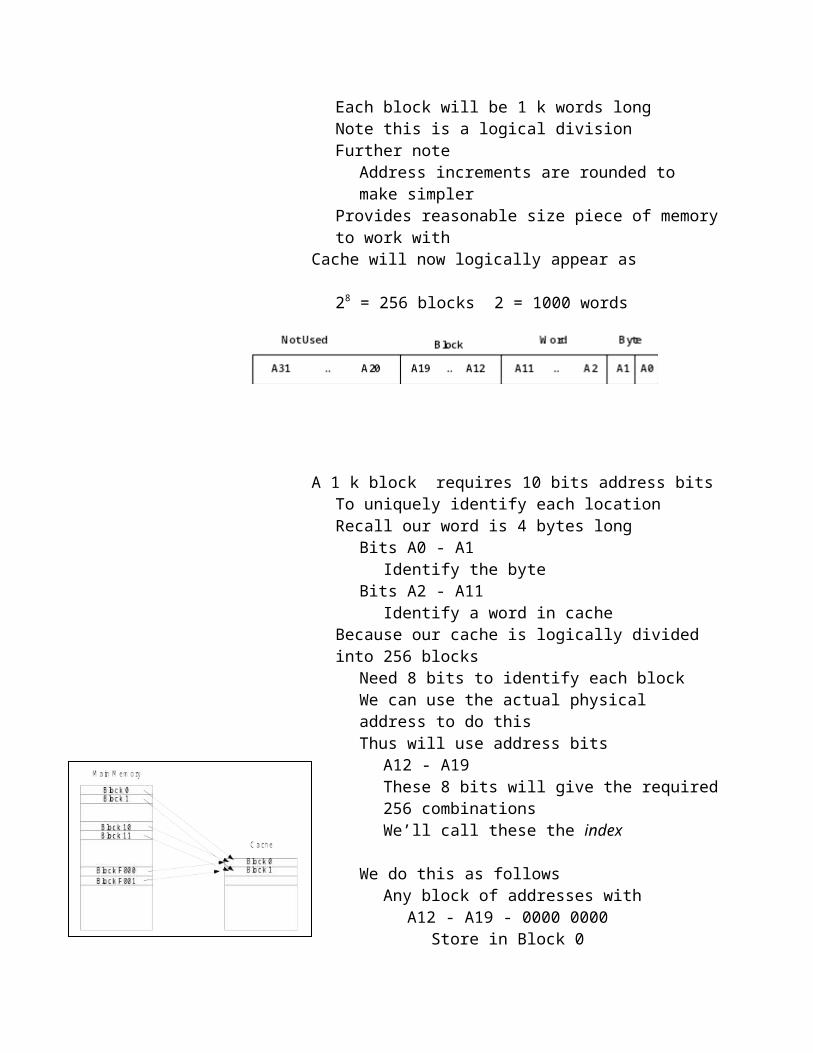
Collection of memory devicesMemory address registerMemory data registerWords will be 32 bitsWill have 256 k word cache
ArchitectureWe will logically divide cache into 256 blocks
Each block will be 1 k words longNote this is a logical divisionFurther note
Address increments are rounded to make simplerProvides reasonable size piece of memory to work with
Cache will now logically appear as
28 = 256 blocks 2 = 1000 words
A 1 k block requires 10 bits address bits To uniquely identify each locationRecall our word is 4 bytes long
Bits A0 - A1Identify the byte
Bits A2 - A11Identify a word in cache
Because our cache is logically divided into 256 blocksNeed 8 bits to identify each blockWe can use the actual physical address to do thisThus will use address bits
A12 - A19These 8 bits will give the required 256 combinationsWe’ll call these the index
We do this as followsAny block of addresses with
A12 - A19 - 0000 0000Store in Block 0
A12 - A19 - 0000 0001Store in Block 1
A12 - A19 - 0000 0010Store in Block 2etc.
A20 - A31Not directly used to address cacheUsed to distinguish
Blocks within cacheCalled a tag

Stored in tag table
Tag TableTag table provides last bit of informationContains
One entry for each block in cacheOurs will contain 256 entries
One for each block
Entry containsBit to indicate if word within block modified
Called dirty bitAddress bits A20 - A31 of corresponding blockBit to indicate block in cache
SummarizingA0 - A1 Identify Byte within a WordA2 - A11 Identify Word within a blockA12 - A19 Identify Block within cacheA20 - A31 Identify Addresses within a Block
Stored in tag table
Finding a wordTo find word in cache execute simple process
Check tag table for bits A20 - A31If present
Use bits A12 - A19 to index into cacheUse bits A2 - A11 to index into blockUse bits A0 - A1 for byte accessif WRITE operation
Set dirty bit in tag tableModify word
else return wordelse
Get block from primary memoryif block occupied
Check dirty bitif set
write block to primary memorywrite block to cacheset occupied bit
elsewrite block to cacheset occupied bit
Data or instruction
Most contemporary computersUse two caches
Data Instruction
Same principles work for bothOnly extra work
Deciding which cache to usePerformance
Factors to consider in each caseWith and without cacheWith cache
With and without missOptimizing size
Affect of look ahead
Associative CacheAlternate approach
Let block be placed anywhere in cacheUse associative search to locate
Organization now appears as

Let’s specify the followingMain memory
8 K with 8 byte blocksCache
2 K with 256 8 byte blocksTag table
256 entries
Main memory block goes anywhere in cacheEntry in tag table is main memory block numberLinear search of tag table not feasible
Let a main memory address be of the form
We find a word as follows
Problem with full associative cacheLong search timeComplexity of underlying logic
Let’s now look at scheme that combines features ofDirect mappingAssociative mapping

Called block set associative
Block Set Associative Approach combining direct and associative mappingMain memory organized as collection of groups
Each group comprises number of blocksCache memory organized as collection of sets
Containing specified number of blocksSet number corresponds to main memory group number
Any block from group j can be placed into set jSet is now searched associatively
Far less complex searchDealing with smaller search space
Organization now appears as
Let’s specify the followingMain memory
8 K with 8 byte blocksCache
2 K with 256 8 byte blocksTag table
256 entries
Our addresses have the following association
We can now see how a main memory address IMapped to a cache address

Computation of address follows in same manner asDirect and associative mappings
Intel PentiumImplements separate
Data and instruction cachesEach uses 2 way block set associative scheme
Virtual MemoryVirtual memory is a scheme
Very much like cachingDifference
Caching between primary memory and CPUVirtual memory works between secondary and primary memories
Translates From logical address - program To physical address = primary memory
When information not found in cachePrimary memory checked
When information not found in primary memorySecondary memory checked
In essence primary memory acts as cache for secondary memory
Purpose two foldTake advantage of speed of primary memoryCreate the appearance of unlimited primary memory
High Level AnalysisAs we saw with cache schemeSize of primary memory significantly smaller than secondaryRather than blocks
Primary memory divided into pagesWould like each program to have memory space allocated when loaded
Will assume memory space is contiguousWould like to be to place pages anywhere in primary memory
Makes addressing only slightly more complicatedWill store location of program memory in page tableSimilar to tag table in cache scheme
General retrieval algorithm similar to what we’ve seenProgram begins executingEncounters needed data or instruction

Check cacheIf in cache
Have a cache hitUse
ElseHave cache missCheck primary memoryIf in primary
Bring associated block into cacheElse
Have a page faultGet from secondary memoryMust make roomRemove existing page
If page has been modifiedSave changes
ElseDiscardWrite new page in its placeBring associated block into cache
ImplementationDesign primary memory
HardwareCollection of memory devicesMemory address registerMemory data registerWords will be 32 bitsWill have 16 M byte primary memory
ArchitectureWe will logically divide primary memory into 210 4k pages
Each page will be 4k words longEach will hold 4 blocksEach block will hold 1 K words
Note this is a logical divisionFurther note
Again address increments are rounded to make simplerProvides reasonable size piece of memory to work with
Primary memory will now logically appear asNote j not necessarily = i + 1We consider a
Virtual address Primary memory address

Secondary memory address
Assume Virtual Memory has212 pages
Assume Secondary Memory has218 pages 1 G words or 4 G bytes
Similar to cacheA2 - A11
Identifies word in page
Assume Main Memory has 210 pages – 1000 pages
Identified by bits A23 - A14Now
A13 - A12Identify block in page
A11 - A2Identify word in block
A1-A0Byte within a word
Page table Contains one entry for each of your possible page in secondary memory
Our design will have 218 entriesYour pages can be anywhere in secondary memory
To your program they appear at 0, 1, 2…m-1
Could also have Page tables i, j, and k etc.
Alternately useA31 - A24 to identify one of 256 page tables
Potentially allows for upto 256 jobs in memoryWhen job enters system
Page table included

May have only subset of your pages in memory at any one timeA23 - A14 to identify a page within a page table
From point of view of virtual memory address
Page number represents an offset into the page table
Valid bit to indicate if page in primary memoryEntry contains pointer to location in main memoryIf not in main memory
Point to location in secondary memory
Dirty bit to indicate modified data
VM Page Number Page Address Status Location in MM or SM0 0-4095 01 4096-8191 22 1
13127 123
7212 …. 55
Address calculation proceeds as with cacheOnce we find the pages in primary memoryWhen program loaded
Primary memory space allocatedAmount depends upon program
Address of allocated spaceStored in page table register
Gives starting address of allocated space

To find pagesGo to page tableAdd
Contents of page table register to A31 - A14 of virtual address
Gives index into page tableAddress
Physical memory if therePointer to secondary memory otherwise
Use A13 - A12 to identify block
Page ReplacementClearly primary memory of limited size
16 M bytesWe have the ability to address
4 G wordsAlthough 16 M seems like lot
Do not want to restrict program to that sizeTo satisfy requirements will need to be able to

Load additional pages into memoryAs long as space left no problemIf no space
Must remove somethingSeveral schemes available each has advantages and disadvantagesAll require checking dirty bit prior to removal
If set Write operation necessary
Otherwise Overwrite page
Two most commonRequire time stamp on each pageLRU
Remove least recently used pageAlso called FIFOAssumes oldest page least likely to be used in future
MRURemove most recently used pageAlso called LIFOAssumes newest page least likely to be used in future
RandomSelect and remove page at randomEasy to implement
PerformanceWith and without VMWith VM
With and without page faultOptimizing size
Speeding things up - TLBOur virtual memory page table
Contains information for 218 pagesSearch process and address calculation
Can be very time consumingWould like to improve response timeEasiest way
Use caching techniques learned earlierKeep in memory a cache containing
Most recently used page addressesCalled Translation Look Aside Buffer - TLBSearch for a page begins in the TLBIf not found then check page table as before
Architecture

Choose 256 entries256 most recently calculated addresses stored
Implement associative search Keyed on virtual memory page number
Each entry must containValid Bit
Indicates if entry is validDirty Bit
Indicates if entry has been changedTag
A31 - A14 of virtual addressPhysical Page
Computed address of page in primary memory