Introduction to Electron Microscopy; Scanning Electron...
54
Transcript of Introduction to Electron Microscopy; Scanning Electron...

Introduction to Electron Microscopy;Scanning Electron Microscopy (SEM)
Harini SosiatiProdi Teknik Mesin, Fakultas Teknik
Universitas Muhammadiyah Yogyakarta

1. THEORY OF SCANNING ELECTRON MICROSCOPE (SEM)
2. SEM SPECIMEN PREPARATIONS
3. CHARACTERIZATION AND INTERPRETATION OFSEM AND SEM-EDS RESULTS
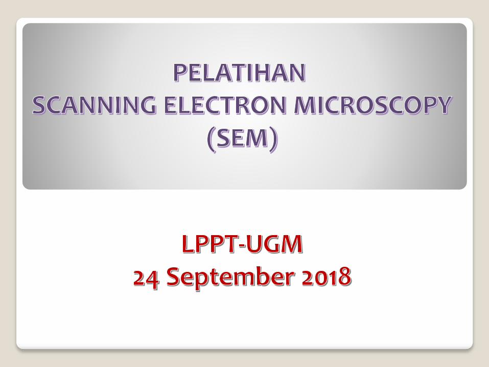
ELECTRON MICROSCOPY:
- Scanning electron microscopy (SEM)
- Transmission electron microscopy (TEM)
- High voltage electron microscopy (HVEM)
- Scanning transmission electron microscopy (STEM)
ANALYTICAL SEM:
- SEM-EDS (energy dispersive x-ray spectroscopy)
BRIEF INTRODUCTION TO ELECTRON MICROSCOPY
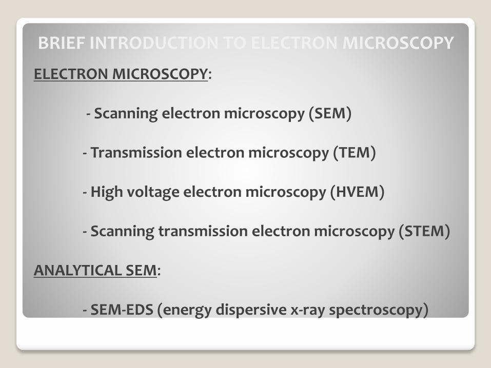
Wave length of light and electron
LIGHT
ELECTROMAGNETIC
WAVE
The wave length of
ELECTRON is
dependent on the
accelerating voltage
Why should we use electron microscope?
Accelerating voltage Wave length of
electron (, nm)
20 kV 0.00859
120 kV 0.00335
200 kV 0.00251
1000 kV 0.00087
Species of light Wave length (, nm)
Electric wave 106~1012
Ultra red light 103~105
Visible light 390~760
Ultra violet light 13~390
X-ray 0.05~10
-ray 0.005~0.1

The difference between optical and electron microscope
Resolution 0.2 mm (OM) 0.2 nm (TEM) 1.5 nm (SEM)

SEM images of martensite structure.

(c)
TEM images of martensite structure. (a) and (c) Bright field (BF TEM images) and(b) Lattice image.
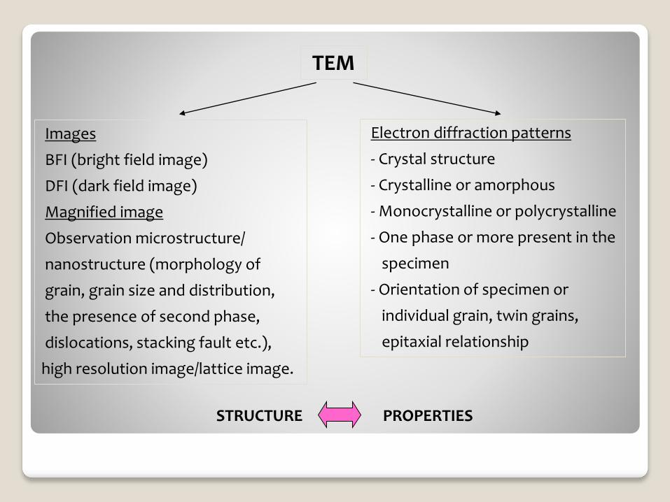
TEM
Images
BFI (bright field image)
DFI (dark field image)
Magnified image
Observation microstructure/
nanostructure (morphology of
grain, grain size and distribution,
the presence of second phase,
dislocations, stacking fault etc.),
high resolution image/lattice image.
Electron diffraction patterns
- Crystal structure
- Crystalline or amorphous
- Monocrystalline or polycrystalline
- One phase or more present in the
specimen
- Orientation of specimen or
individual grain, twin grains,
epitaxial relationship
STRUCTURE PROPERTIES
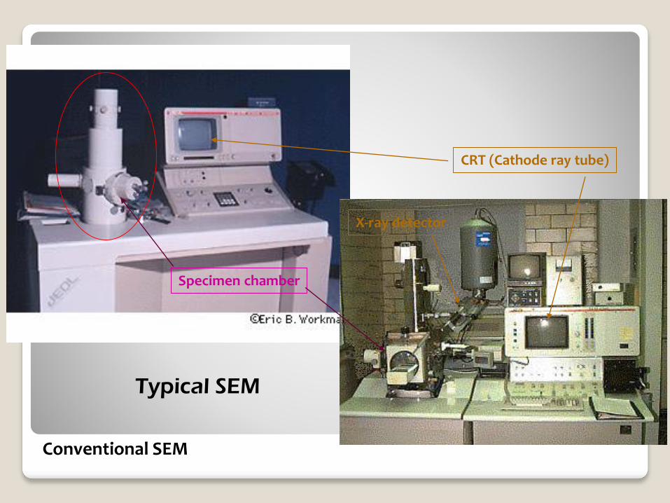
Conventional SEM
Specimen chamber
CRT (Cathode ray tube)
X-ray detector
Typical SEM

SEM-EDS

Typical TEM
JEM-1400
(MIPA UGM) Tecnai-20FLorentz TEM
TEM-EDXS
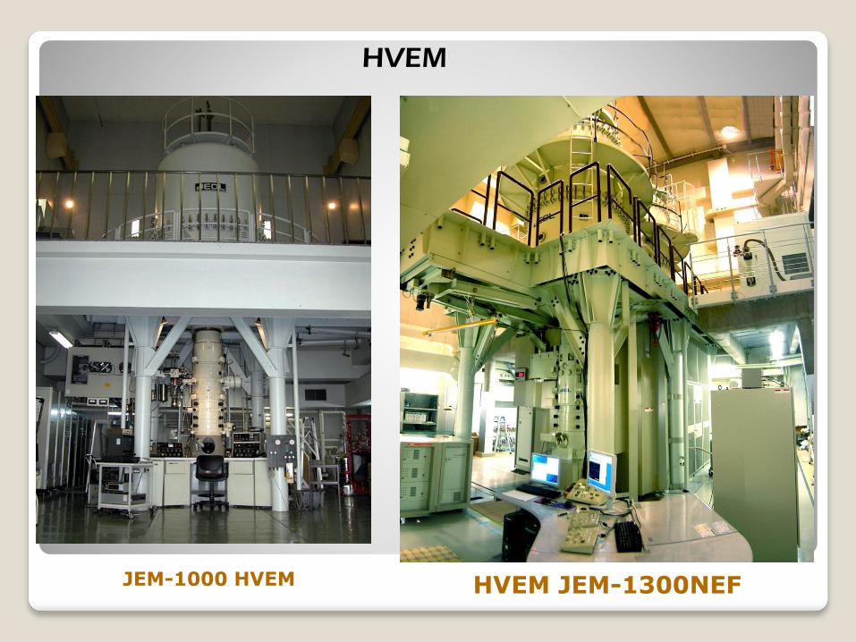
HVEM
HVEM JEM-1300NEFJEM-1000 HVEM

An electron microscope cannot see the wood for the tree
An electron microscope is just for seeing trees
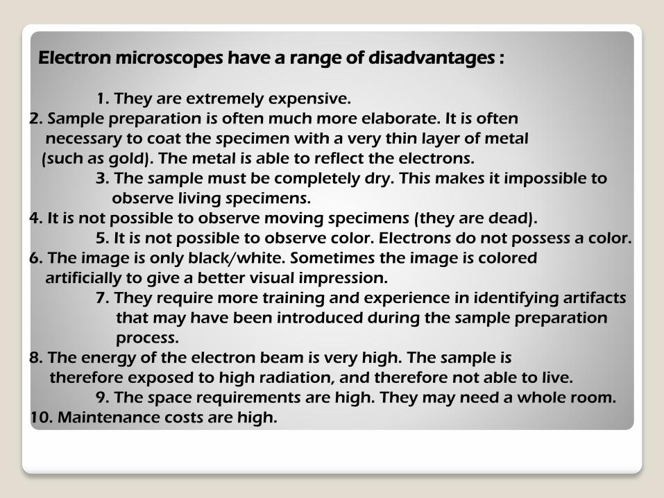
Electron microscopes have a range of disadvantages :
1. They are extremely expensive.
2. Sample preparation is often much more elaborate. It is often
necessary to coat the specimen with a very thin layer of metal
(such as gold). The metal is able to reflect the electrons.
3. The sample must be completely dry. This makes it impossible to
observe living specimens.
4. It is not possible to observe moving specimens (they are dead).
5. It is not possible to observe color. Electrons do not possess a color.
6. The image is only black/white. Sometimes the image is colored
artificially to give a better visual impression.
7. They require more training and experience in identifying artifacts
that may have been introduced during the sample preparation
process.
8. The energy of the electron beam is very high. The sample is
therefore exposed to high radiation, and therefore not able to live.
9. The space requirements are high. They may need a whole room.
10. Maintenance costs are high.

SEM(Theory and Analysis)
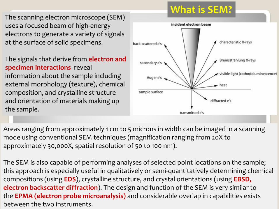
The scanning electron microscope (SEM) uses a focused beam of high-energy electrons to generate a variety of signals at the surface of solid specimens.
The signals that derive from electron and specimen interactions reveal information about the sample including external morphology (texture), chemical composition, and crystalline structure and orientation of materials making up the sample.
What is SEM?
Areas ranging from approximately 1 cm to 5 microns in width can be imaged in a scanning mode using conventional SEM techniques (magnification ranging from 20X to approximately 30,000X, spatial resolution of 50 to 100 nm).
The SEM is also capable of performing analyses of selected point locations on the sample; this approach is especially useful in qualitatively or semi-quantitatively determining chemical compositions (using EDS), crystalline structure, and crystal orientations (using EBSD, electron backscatter diffraction). The design and function of the SEM is very similar to the EPMA (electron probe microanalysis) and considerable overlap in capabilities exists between the two instruments.

Incident electrons(electron probe)
Secondary Electrons(100 Å)
Backscattered Electrons(< 1-2 m)
Characteristic X-rays
Auger Electrons(10 – 30 Å)
Continuum X-rays
Fluorescent X-rays
Electron beam interaction diagram
5
m

The penetration of the beam into the mass of the specimen is determined
by basically 4 parameters: beam current, spot size, accelerating voltage
and atomic number of the specimen.

Fundamental Principles of Scanning Electron Microscopy (SEM)
Secondary electrons and backscattered electrons are commonly used for imagingsamples: secondary electrons are most valuable for showing morphology andtopography on the specimen and backscattered electrons are most valuable forillustrating contrasts in composition in multiphase samples (i.e. for rapid phasediscrimination).
Emission of secondary electrons occurs in the process where incident electrons penetrate a specimen and then inelastically scattered. A free electron in the specimen may receivean electrostatic force (Coulomb force) from the incident electron or scattered electronand thereby part of the latter’s energy and then jump out into the vacuum. This electronIs called a secondary electron.However, the energy received by freeelectron is as small as a few ten eV max. Therefore, it has been though that only the secondary electron produced within a depthrange about 10 nm below the specimen surfacecan escape into the vacuum.

Electron scattering in a specimen are classifiedinto 2 types; 1. elastic scattering in which incident electron are scattered at a large angle with almostno loss in energy. 2. Inelastic scattering in which incident electron Loose energy but are scattered at a small angle.
The elastically scattered electrons having approximately the same energy as the incidentelectrons are scattered from the vicinity of specimen surface into the vacuum, while inelastically scattered electrons which have lost energy substantially are scattered from a Comparatively deep location in the specimenInto the vacuum.
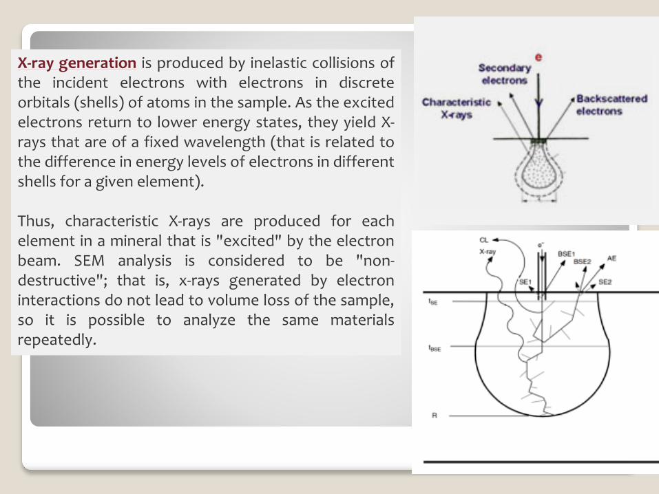
X-ray generation is produced by inelastic collisions ofthe incident electrons with electrons in discreteorbitals (shells) of atoms in the sample. As the excitedelectrons return to lower energy states, they yield X-rays that are of a fixed wavelength (that is related tothe difference in energy levels of electrons in differentshells for a given element).
Thus, characteristic X-rays are produced for eachelement in a mineral that is "excited" by the electronbeam. SEM analysis is considered to be "non-destructive"; that is, x-rays generated by electroninteractions do not lead to volume loss of the sample,so it is possible to analyze the same materialsrepeatedly.


EDS Principle
Energy Dispersive X-ray Spectroscopy (EDS orEDX) is a qualitative and quantitative X-raymicroanalytical technique that providesinformation on the chemical composition of asample for elements with atomic number (Z)>3.
Characteristic X-ray Generation
The atoms are ionized by the primary electronbeam leading to holes generated on the coreshells; following ionization the electrons fromouter shells fill the holes and cause theemission of X-ray fluorescence lines.
The characteristic X-ray lines are namedaccording to the shell in which the initialvacancy occurs and the shell from which anelectron drops to fill that vacancy.
For instance, if the initial vacancy occurs inthe K shell and the vacancy filling electrondrops from the adjacent (L) shell, a Kα x-ray isemitted. If the electron drops from the Mshell (two shells away), the emitted x-ray is aKβ x-ray. Similarly, if an L-shell electron isejected and an electron from the M-shell fillsthe vacancy, Lα radiation will be emitted.

Examples
SE analysis:
TOPOGRAPHY
BSE analysis:
COMPOSITION
Heavy elements (high atomic number) backscatter electrons more strongly
than light elements (low atomic number) appear brighter in the image
All the elements have different sized nuclei.
As the size of the atom nucleus increases,
the number of BSE increases.
Thus, BSE can be used to get an image that
showed the different elements present in a sample.

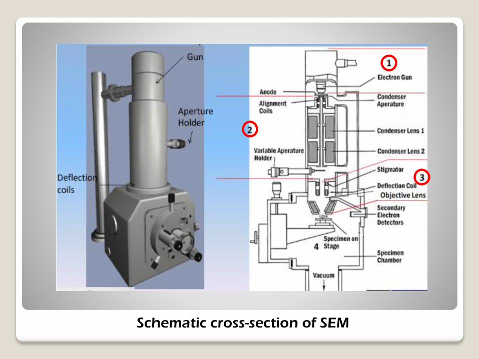
Schematic cross-section of SEM
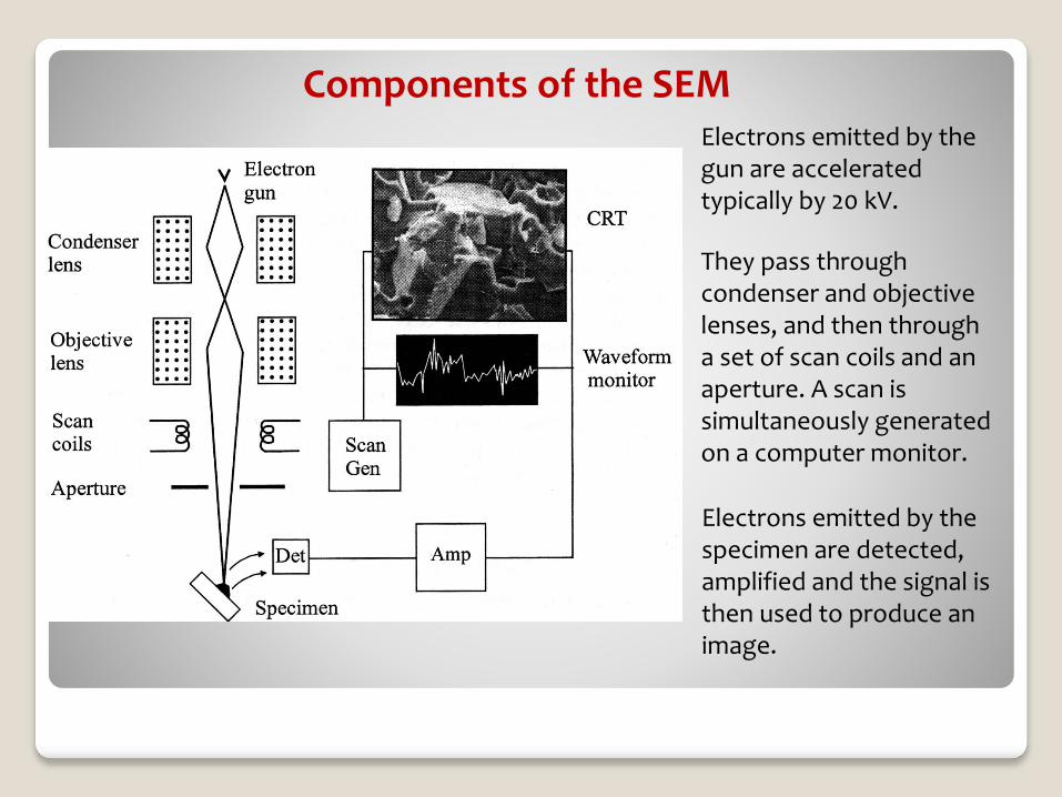
Electrons emitted by the gun are accelerated typically by 20 kV.
They pass through condenser and objective lenses, and then through a set of scan coils and an aperture. A scan is simultaneously generated on a computer monitor.
Electrons emitted by the specimen are detected, amplified and the signal is then used to produce an image.
Components of the SEM
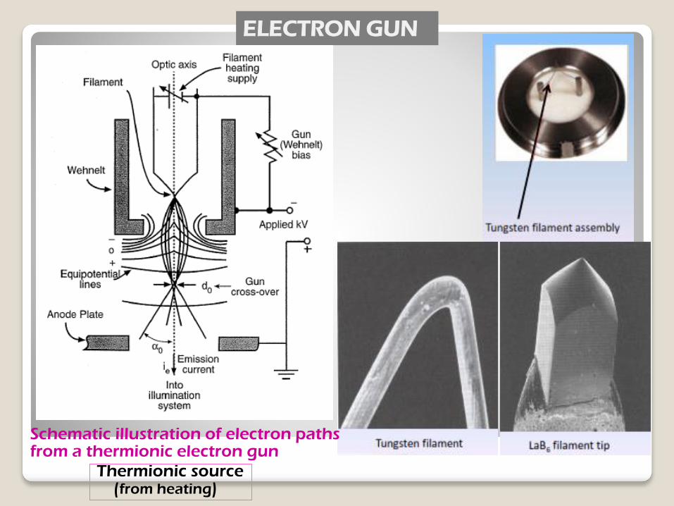
ELECTRON GUN
Schematic illustration of electron pathsfrom a thermionic electron gun
Thermionic source(from heating)

Schematic illustration of electron pathsfrom a field emission gun
Field-emission source(from electric field)
W field-emission
filament

Comparison of three types of source operating at 100 kV


Vacuum system
Category of vacuum (1 Torr130 Pa, 1 Pa= 7.5x10⁻³ Torr)
All electron microscopes are operated under vacuum:
-To keep specimen clean (less contamination)
-To not reduce lifetime of filament
-To avoid contaminant in the column
-To improve image resolution

Resolution in the SEM
The resolution of the SEM is determined by the size of the incident beam. This can be reduced by introducing an aperture unto the beam path and by reducing the probe size using the condenser lens. Note that reducing the probe size using the condenser lens also reduces the beam current (for an explanation, see Goodhew et al., p. 131). Therefore, as you reduce the probe size you eventually reach a point where imaging is impossible. For a typical SEM operating at 20 kV, the minimum usable probe size is of the order of 1 – 3 nm.
Resolution also depends on accelerating voltage. This is because higher energy electrons experience less spherical aberration when they pass through the lenses. Resolution is also improved by reducing the working distance, up to a certain point. Beyond that point the lenses may not be able to focus the beam on the sample.
As already noted, images obtained with backscattered electrons have a lower resolution than these obtained with secondary electrons, because they originate from deeper within the specimen.

Depth of field 1
Depth of field is the distance above and below the plane of optimum focus within which the image is in focus.
In the diagram on the right, drepresents the diameter of the electron beam at the specimen. The depth of field is h, since it makes no difference to the sharpness of the image if the object is anywhere within the range h.
Reducing the angle α increases the depth of field. This can be achieved by using a smaller aperture or by increasing the working distance.

Depth of field 2
These diagrams illustrate the effect of the convergence angle α on the depth of field.
Because of the geometry of the imaging system, scanning electron microscopes have a much greater depth of field than optical microscopes .

Astigmatism 1
Astigmatism is a problem that is commonly encountered in SEM (and TEM). Itis an aberration of lenses that causes rays in a plane parallel to the opticalaxis to be focused at a different focal point from rays in a plane at 90° to it.The effect of astigmatism is that objects in the image generally appear“stretched” in one direction, and then in the other direction as you gothrough focus.
All electron microscopes are equipped with stigmators, which allow theuser to correct the astigmatism, as shown in the next slide. Properlycorrected astigmatism is essential in achieving high resolution images.


Astigmatism 2
The SEM images shown below left illustrate how astigmatism affects theimage as you go through focus. On the right is shown the image followingcorrection with the stigmators.
Astigmatic Corrected

SEM SPECIMEN PREPARATION
SPECIMENS:1. Powder
2. Bulk Specimens:Metals/alloysCeramicsMineralsNatural fibersNanofiber membranes etc.
3. Biological materials
4. Specimens containing oil

SPECIMEN PREPARATION
1. For small particles (powder, <100 nm)E
than
ol
2. For small particles (powder, >100 nm)
MOST IMPORTANT: DISPERSION !!
SpecimenSpecimen holder
C-tape
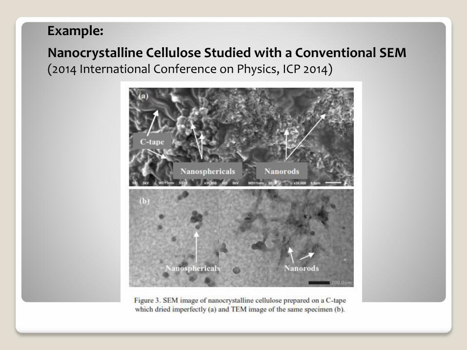
Nanocrystalline Cellulose Studied with a Conventional SEM(2014 International Conference on Physics, ICP 2014)
Example:


For conventional imaging in the SEM, specimen must be electrically conductive at least at the specimen surface and electrically grounded to prevent the accumulation of electrostatic charge at the surface during electron irradiation.
For the specimen that is enough conductivity, two important reasons for coating are to maximize signal and improve the spatial resolution.
Target: Au, Au-Pd alloy, Pt, W, C
Non-conductive specimen
Coating layer

Ze
oli
tes
- No dried in an
oven (120°C, 1 h)
- C-coating
- dried in an
oven (120°C, 1 h)
- C-coating
Charge-up
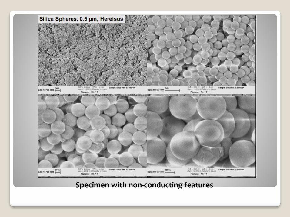
Specimen with non-conducting features

What is the charge-up phenomenon ?
Charge-up occurs during observation of non-conductive specimens
The charge-up phenomenon can be overcome as follows.1. Reduce the accelerating voltage2. Reduce the specimen irradiating current3. Apply the metal coating4. Observe image in low vacuum mode5. Utilize a low-acceleration BSE signal.
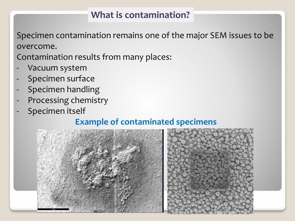
What is contamination?
Specimen contamination remains one of the major SEM issues to beovercome.Contamination results from many places:- Vacuum system- Specimen surface- Specimen handling- Processing chemistry- Specimen itself
Example of contaminated specimens

The phenomenon by which gas molecules of hydrocarbons existing around the specimen due to electron beam irradiation, then bond together and adhere to the specimen surface is referred to as contamination.With the electron beam irradiating the sample, the clarity of the image at that area decreases and become darker due to the matter accumulated on the specimen surface suppresses the discharge of secondary electron from the specimen.
Contamination can be reduced by the following methods:- Reduction of residual gas molecules in the specimen chamber- Reduction of gas molecules derived from specimen.
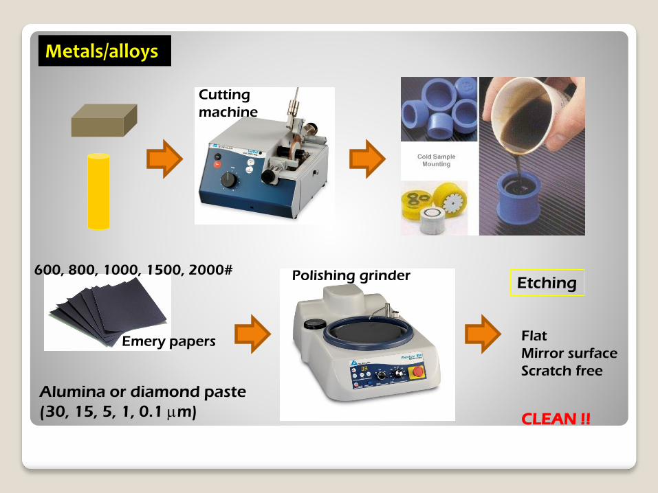
Metals/alloys
600, 800, 1000, 1500, 2000#
Alumina or diamond paste
(30, 15, 5, 1, 0.1 m)
Etching
Flat
Mirror surface
Scratch free
Emery papers
CLEAN !!
Cutting
machine
Polishing grinder

Zeolite Kenaf fibers
Printed circuit board (PCB)
Sn plated Cu
Plan-view of oxidized/corroded surface

General preparation for biological specimens
Such Specimens are usually observed in dried condition since theInterior of the electron microscope is evacuated.
Perfusion fixation(Substitution of fixative solution with blood and glutsraldehyde, formalin, etc.
Fine sectioning of specimen
Immersion fixation (Glutaraldehyde, formalin etc)
Post-fixation (Osmium tetraxide)
Conductive staining (Tannic acid-osmium tetroxide etc.)
Dehydration (Ethanol series, etc.)
Drying (Critical point drying, freeze drying etc.)
Observation with a SEM
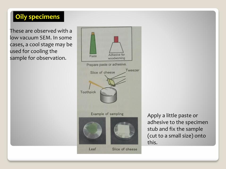
Oily specimens
These are observed with a low vacuum SEM. In somecases, a cool stage may be used for cooling the sample for observation.
Apply a little paste or adhesive to the specimen stub and fix the sample (cut to a small size) onto this.
CHARACTERIZATION AND INTERPRETATION OFSEM AND SEM-EDS RESULTS
Some examples and discussion