![f3k 0504 1000 m64 hynix[68032 a[1].4]notebookschematic.org/data/NOTEBOOK/attachments/SC... · test21 ab8 test20 af7 test28_h j7 test28_l h8 test27 af8 test26 ae6 test10 k8 test8 c4](https://static.fdocuments.in/doc/165x107/5fa937090f10aa6d031801d8/f3k-0504-1000-m64-hynix68032-a14-test21-ab8-test20-af7-test28h-j7-test28l.jpg)
INTRODUCTION TO ADVAN CED SYSTEM-ON … · 5.1.4 Simulated Annealin g 18 5.1.5 Genetic Al gorithms...
30
INTRODUCTION TO ADVANCED SYSTEM-ON-CHIP TEST DESIGN AND OPTIMIZATION
Transcript of INTRODUCTION TO ADVAN CED SYSTEM-ON … · 5.1.4 Simulated Annealin g 18 5.1.5 Genetic Al gorithms...

INTRODUCTION TO ADVANCED SYSTEM-ON-CHIP TEST DESIGN
AND OPTIMIZATION

FRONTIERS IN ELECTRONIC TESTING
Consulting Editor
Vishwani D. Agrawal
Books in the series:
Embedded Processor-Based Self-Test
D. Gizopoulos
ISBN: 1-4020-2785-0
Testing Static Random Access Memories
S. Hamdioui
ISBN: 1-4020-7752-1
Verification by Error Modeling
K. Radecka and Zilic
ISBN: 1-4020-7652-5
Elements of STIL: Principles and Applications of IEEE Std. 1450
G. Maston, T. Taylor, J. Villar
ISBN: 1-4020-7637-1
Fault Injection Techniques and Tools for Embedded systems Reliability
Evaluation
A. Benso, P. Prinetto
ISBN: 1-4020-7589-8
High Performance Memory Memory Testing
R. Dean Adams
ISBN: 1-4020-7255-4
SOC (System-on-a-Chip) Testing for Plug and Play Test Automation
K. Chakrabarty
ISBN: 1-4020-7205-8
Test Resource Partitioning for System-on-a-Chip
K. Chakrabarty, Iyengar & Chandra
ISBN: 1-4020-7119-1
A Designers' Guide to Built-in Self-Test
C. Stroud
ISBN: 1-4020-7050-0Boundary-Scan Interconnect Diagnosis
J. de Sousa, P.Cheungy
ISBN: 0-7923-7314-6Essentials of Electronic Testing for Digital, Memory, and Mixed Signal VLSI Circuits
M.L. Bushnell, V.D. Agrawal ISBN: 0-7923-7991-8
Analog and Mixed-Signal Boundary-Scan: A Guide to the IEEE 1149.4 Test Standard
A. OsseiranISBN: 0-7923-8686-8
Design for At-Speed Test, Diagnosis and MeasurementB. Nadeau-DostiISBN: 0-79-8669-8
Delay Fault Testing for VLSI CircuitsA. Krstic, K-T. Cheng
gg
ISBN: 0-7923-8295-1Research Perspectives and Case Studies in System Test and Diagnosis
J.W. Sheppard, W.R. Simpsonp
ISBN: 0-7923-8263-3Formal Equivalence Checking and Design Debugging
S.-Y. Huang, K.-T. Chengq gg
ISBN: 0-7923-8184-XDefect Oriented Testing for CMOS Analog and Digital Circuits
M. SachdevISBN: 0-7923-8083-5

by
ERIK LARSSONLinköpings University, Sweden
INTRODUCTION TO ADVANCED
SYSTEM-ON-CHIP TEST DESIGN
AND OPTIMIZATION

A C.I.P. Catalogue record for this book is available from the Library of Congress.
ISBN-10 1-4020-3207-2 (HB) Springer Dordrecht, Berlin, Heidelberg, New YorkISBN-10 0-387-25624-5 (e-book) Springer Dordrecht, Berlin, Heidelberg, New YorkISBN-13 978-1-4020-3207-3 (HB) Springer Dordrecht, Berlin, Heidelberg, New YorkISBN-13 978-0-387-25624-5 (e-book) Springer Dordrecht, Berlin, Heidelberg, New York
Published by Springer,
P.O. Box 17, 3300 AA Dordrecht, The Netherlands.
Printed on acid-free paper
All Rights Reserved
© 2005 Springer
No part of this work may be reproduced, stored in a retrieval system, or transmitted
in any form or by any means, electronic, mechanical, photocopying, microfilming, recording
or otherwise, without written permission from the Publisher, with the exception
of any material supplied specifically for the purpose of being entered
and executed on a computer system, for exclusive use by the purchaser of the work.
Printed in the Netherlands.

Contents
Preface xiii
Acknowledgements xvii
Part 1 Testing concepts
1. INTRODUCTION 1
2. DESIGN FLOW 5
1 Introduction 5
2 High-level design 6
3 Core-Based Design 73.1 Network-on-Chip 93.2 Platform-Based Design 9
4 Clocking 104.1 System Timing 114.2 Clock Distribution 114.3 Multiple Clock Domains 12
4.3.1 Phase Locked Loop (PLL) 124.3.2 Globally-Asynchronous Locally-Synchronous 13
5 Optimization 145.1 Optimization Techniques 16
5.1.1 Backtracking and Branch-and-bound 165.1.2 Integer Linear Programming 175.1.3 Local Search 175.1.4 Simulated Annealing 185.1.5 Genetic Algorithms 185.1.6 Tabu Search 19

SOC Test Designvi
3. DESIGN FOR TEST 21
1 Introduction 211.1 Fault models 21
1.1.1 Stuck-at Fault Model 221.1.2 Bridging Fault Model 221.1.3 Stuck-Open Fault Model 231.1.4 Delay Fault Model 23
1.2 Test Generation for Combinational Circuits 241.2.1 Path Sensitization 251.2.2 Boolean Difference 251.2.3 D-algorithm 261.2.4 PODEM (Path-Oriented Decision-Making) 271.2.5 FAN (Fanout-Oriented Test Generation) 281.2.6 Subscripted D-Algorithm 281.2.7 CONcurrent Test Generation 281.2.8 Fault Simulation 281.2.9 Optimization 281.2.10 Delay Fault Detection 30
1.3 Testing Sequential Circuits 30
2 Design-for-Test Methods 312.1 Test Point Insertion 322.2 The Scan Technique 32
2.2.1 Scan Testing for Delay Faults 362.3 Test Pattern Generation for BIST 39
2.3.1 Exhaustive Pattern Generation 402.3.2 Pseudo-Random Pattern Generation 402.3.3 Pseudo-random-based test generation 402.3.4 Deterministic Testing 41
2.4 Test Response Analysis for BIST 412.5 Circular-BIST 432.6 BIST-Architectures 43
2.6.1 BILBO (Built-In Logic Block Observer), 432.6.2 STUMPS Architecture 442.6.3 LOCST (LSSD On-Chip Self-Test) 44
2.7 Memory Testing 452.7.1 Algorithmic Test Sequence (ATS) 482.7.2 Marching Pattern Sequences (MARCH) 482.7.3 Checkboard Test 492.7.4 Memory BIST 492.7.5 Memory Diagnosis and Repair 50
3 Mixed-Signal Testing 51

Contents vii
4. BOUNDARY SCAN 53
1 Introduction 53
2 The Boundary-Scan Standards (IEEE 1149.1) 532.1 Registers 562.2 TAP Controller 572.3 Instructions 57
2.3.1 Example 572.3.2 Boundary-Scan Languages 582.3.3 Cost of Boundary Scan 58
3 Analog Test Bus (IEEE 1149.4) 613.1 Analog Test Access Port (ATAP) 633.2 Test Bus Interface Circuit (TBIC) 633.3 Analog Boundary Module (ABM) 633.4 Instructions 633.5 Chaining Example 63
Part 2 SOC Design for Testability
5. SYSTEM MODELING 67
1 Introduction 67
2 Core modeling 68
3 Test Resource modeling 71
4 Core Wrapper 72
5 Test Access Mechanism 74
6. TEST CONFLICTS 77
1 Introduction 77
2 Limitations at the Tester 782.1 Bandwidth Limitations 792.2 Tester Memory Limitations 792.3 Test Channel Clocking 80
3 Test Conflicts 813.1 General Test Conflicts 813.2 Multiple Test Set 823.3 Multiple Sets of Test Sets 823.4 Interconnection Testing - Cross-Core Testing 843.5 Hierarchy - Cores Embedded in Cores 85
4 Discussion 86

SOC Test Designviii
7. TEST POWER DISSIPATION 89
1 Introduction 89
2 Power consumption 90
3 System-level Power modeling 91
4 Hot-spot modeling with Power Grids 93
5 Core-level Power modeling 95
6 Discussion 98
8. TEST ACCESS MECHANISM 99
1 Introduction 991.1 System-on-Chip Test Data Transportation 100
1.1.1 The TestShell and P1500 Approach 1001.2 Reconfigurable Core Wrappers 106
2 Test Access Mechanism Design 1072.1 Multiplexing Architecture 1082.2 Distribution Architecture 1092.3 Daisychain Architecture 1102.4 Test Bus Architecture 1112.5 TestRail Architecture 1112.6 Flexible-Width Architecture 1122.7 Core Transparancy 112
3 Test TIME Analysis 113
9. TEST SCHEDULING 115
1 Introduction 115
2 scheduling of Tests with fixed test time under test conflicts 1192.1 Preemptive test scheduling 128
3 scheduling of tests with non-fixed (variable) testing times 1283.1 Idle Types 128
3.1.1 Imbalanced TAM Test Completion Times 1293.1.2 Module Assigned to TAM of Non Pareto Optimal
Width 1303.1.3 Imbalanced Scan Chains in Module 1313.1.4 Other Types of Idle Bits 131
3.2 SOC Test Scheduling with Fixed-Width TAM 1323.3 SOC Test Scheduling with Flexible-Width TAM 134
3.3.1 Test Power 1373.3.2 Multiple Test Sets 138

Contents ix
3.4 Other Test Scheduling Techniques 1383.4.1 Problem: Control lines and Layout. 1383.4.2 Problem: Power Modeling 1383.4.3 Problem: Fixed Test Resources 1393.4.4 Problem: Multiple Clock Domains 1403.4.5 Problem: Delay Fault Testing 1403.4.6 Defect-Oriented Scheduling 140
4 Optimal Test time? 1434.1 Soft Cores - No Fixed Scan-chains 1464.2 Hard Cores - Fixed Number of Scan-chains 150
5 Integrated Test Scheduling and TAM Design 1515.1 Test Time and Test Power Consumption 1525.2 Bandwidth Assignment 1525.3 Test Scheduling 1535.4 TAM Planning 1545.5 TAM Optimization 156
6 Integrating Core Selection in the Test Design Flow 157
7 Further Studies 1607.1 Combined Test Time and TAM Design Minimization 1607.2 Core Selection in the Test Design Flow 1607.3 Defect-Oriented Test Scheduling 160
Part 3 SOC Test Applications
10. A RECONFIGURABLE POWER-CONSCIOUS CORE WRAPPERAND ITS APPLICATION TO SYSTEM-ON-CHIP TESTSCHEDULING 163
1 Introduction 163
2 Background and Related Work 165
3 A Reconfigurable Power-Conscious Core Wrapper 167
4 Optimal Test Scheduling 1704.1 Optimal Scheduling of Core Tests 1714.2 Transformations for Optimal TAM Utilization 1734.3 Cross-Core Test Scheduling 1754.4 Optimal Power-Constrained Scheduling 1774.5 Minimization of TAM Wiring 179
5 Experimental Results 180
6 Conclusions 182

SOC Test Designx
11. AN INTEGRATED FRAMEWORK FOR THE DESIGN AND OPTI-MIZATION OF SOC TEST SOLUTIONS 187
1 Introduction 187
2 Related Work 188
3 System modeling 192
4 The SOC Test Issues 1944.1 Test Scheduling 1944.2 Power Consumption 1954.3 Test Source Limitations 1974.4 Test Set Selection 1974.5 Test Access Mechanism 1984.6 Test Floor-planning 200
5 The Heuristic Algorithm 201
6 Simulated Annealing 2056.1 The Simulated Annealing Algorithm 2056.2 Initial Solution and Parameter Selection 2066.3 Neighbouring Solution in Test Scheduling 2066.4 Neighbouring Solution in Scheduling and TAM Design 2066.5 Cost function 207
7 Experimental Results 2087.1 Benchmarks 2087.2 Test Scheduling 2087.3 Test Resource Placement 2097.4 Test Access Mechanism Design 2097.5 Test Scheduling and TAM Design 211
8 Conclusions 214
12. EFFICIENT TEST SOLUTIONS FOR CORE-BASED DESIGNS 215
1 Introduction 2151.1 Introduction 215
2 Background and Related Work 217
3 Test Problems 2213.1 Test Time 2213.2 Test Power Consumption 2263.3 Test Power Consumption at Test Parallelization 2293.4 Test Resource Limitations 2303.5 Test Conflicts 2313.6 Test Access Mechanism Design 2323.7 System Modeling 233
Contents xi
4 Our Approach 2374.1 Bandwidth Assignment 2384.2 Test Scheduling 2394.3 TAM Planning 2404.4 An Example 2424.5 TAM Optimization 2444.6 Complexity 246
5 Experimental Results 2465.1 Test Scheduling 2465.2 Integrated Test Scheduling and TAM Design 2475.3 Test Scheduling, Test Parallelization and TAM Design 249
6 Conclusions 250
13. CORE SELECTION IN THE SOC TEST DESIGN-FLOW 253
1 Introduction 253
2 BACKGROUND 254
3 Related Work 257
4 Problem Formulation 2604.1 Problem Complexity 263
5 Test Problems and Their Modeling 2635.1 Test Time 2635.2 Test Power Consumption 2645.3 Test Conflicts 267
6 Test Design Algorithm 2686.1 Resource Utilization 2716.2 Example 271
7 Experimental Results 273
8 Conclusions 275
14. DEFECT-AWARE TEST SCHEDULING 277
1 Introduction 277
2 Related Work 278
3 Sequential Test Scheduling 279
4 Concurrent Test Scheduling 2804.1 Test Sets with Fixed Test Times 2814.2 Test Sets with Flexible Test Times 2824.3 Test Scheduling Algorithms 283
5 Experimental Results 286

SOC Test Designxii
6 Conclusions 286
15. AN INTEGRATED TECHNIQUE FOR TEST VECTOR SELECTIONAND TEST SCHEDULING UNDER ATE MEMORY DEPTHCONSTRAINT 291
1 Introduction 291
2 Related Work 293
3 Problem Formulation 295
4 Test Quality Metric 296
5 Test Scheduling and Test Vector Selection 2995.1 Illustrative Example 3015.2 Optimal Solution For Single TAM 305
6 Experimental Results 305
7 Conclusions 307
Appendix 1. Benchmarks 321
1 Introduction 321
2 Format of the inputfile 321
3 Design Kime 324
4 Design Muresan 10 326
5 Design Muresan 20 327
6 ASIC Z 329
7 Extended ASIC Z 331
8 System L 333
9 Ericsson design 335
10 System S 349
References 353
Index 383

Preface
Advances in both semiconductor processing technologies as well as inte-grated circuit (IC) design techniques and tools have enabled the creation ofmicro-electronic products that contain a huge amount of complex functional-ity on a single die. This allows the integration into a single IC of thecomponents that traditionally resided on one or multiple printed circuitboards. As the latter traditional product was commonly referred to as “sys-tem”, a modern IC that contains the same functionality goes by the name“System-On-Chip” or SOC. The benefits of this ongoing integration are obvi-ous: (1) a smaller form factor, as we want small products that fit our pockets,(2) higher performance, as our needs to do, hear, see more with micro-elec-tronics seem insatiable, and (3) lower power, as these portable, mobileproducts work of batteries with a limited energy budget.
Designing SOCs is a challenge. The functional and layout designs need tobe modular and hierarchical, as flat design is no longer an option for such“monster chips”. Increasingly, also the on-chip interconnect becomes hierar-chical; we refer to this as Network-On-Chip or NOC. In order to reduce time-to-market and leverage external expertise, we see large modules beingimported and reused. The latter design practice has divided the IC designcommunity into ‘core providers’ and ‘SOC integrators’.
Testing SOCs brings forward new challenges as well. The only viable wayto contain the growing complexity of SOCs is to apply a modular testapproach. Modular testing is required (1) for heterogeneous SOCs, whichcontain non-logic modules, such as embedded memories, analog and RF mod-ules, e-FPGAs, etc., and (2) for black-boxed third-party cores, for which thetest is developed by the core provider, but applied by the SOC integrator.However, modular testing also has precious benefits in terms of (3) reducedtest pattern generation efforts due to “divide-n-conquer”, and (4) test reuse

SOC Test Designxiv
over multiple generations of SOCs. The research challenges related to a mod-ular test approach are the following.
■ Design and test development is distributed over multiple parties,companies, geographical locations, and time. This brings with it chal-lenges with respect to the transfer of “test knowledge” from core pro-vider to SOC integrator.
■ Cores and other modules are typically deeply embedded within theSOC, without direct access to SOC pins or other test resources.Hence, we need to add an on-chip test access infrastructure, thatenables proper testing of the SOC, but that is as much as possibletransparent when not in test mode.
■ The fact that there is no longer one monolithic chip test, but manysmaller tests instead, brings with it many optimisation issues withrespect to test coverage, test application time, power dissipation dur-ing test, silicon area used by the on-chip infrastructure, etc. Designersand test engineers need support to make the right choices in this com-plex matter, where everything seems to be related with everything.
This book by my fellow researcher Erik Larsson tries to shed light on themany issues that come to play in the arena of modular SOC testing. It waswritten from the need to have a book that could serve as text book for univer-sity students. On the one hand, several text books are available on thefundamentals of classical test approaches. On the other hand, available bookson modular SOC testing have too much a research nature and too little ofintroductory material to serve the purpose of student text book. And indeed,Larsson’s book exactly fits the void in between these two categories.
This book consists of three parts. In Part 1, the book starts out with a briefoverview of classical test approaches. This provides the type of introductionsomeone new in the field will need, with many references to the well-knowntext books for further, in-depth coverage. Part 2 describes the challenges andproblems specific to testing large, modular, and heterogeneous SOCs. Theexperienced reader is suggested to right away jump to this part of the book.Subsequently, Part 3 provides details of the research work Larsson and histeam have done to address these research challenges. The central key word inall these solutions is “integration”; integration of design and test, and integra-tion of solutions to tackle the many multi-faced optimisation problems athand. The entire book is written in the very clear style that also marks Lars-son’s research papers and presentations.

xv
I strongly believe that a modular and hence scalable approach is the onlyfeasible way forward to address the manufacturing test challenges of ICs thatare every-increasing in size and complexity. Hence, I do recommend thisbook; to researchers, to test methodology developers at EDA companies, todesign and test engineers, and of course to university students.
ERIK JAN MARINISSEN
Principal ScientistPhilips Research Laboratories
Eindhoven, The Netherlands

Acknowledgements
This book would not have been written without the help of many. I wouldlike to thank Zebo Peng, Petru Eles, and the rest of the group at EmbeddedSystems Laboratory at the Department of Computer and Information Scienceat Linköpings Universitet, Sweden. I would like to thank Julien Pouget, StinaEdbom, Klas Arvidsson, and Per Beijer for their contributions to the book.And I would like to thank Krishendu Chakrabarty, Erik Jan Marinissen, andVishwani D. Agrawal for comments on the draft. I would like to thank HideoFujiwara for the time in Japan, Mark de Jongh for inspiration and Cindy Zitterfor encouragements, and finally friends and familly.
ERIK LARSSON
Linköpings UniversitetLinköping, Sweden

PART 1TESTING CONCEPTS

Chapter 1
IntroductionThe aim of this book is to discuss production test, including related prob-
lems, their modeling, and the design and optimization of System-on-Chip(SOC) test solutions. The emphasis is on test scheduling, how to organize thetesting, which is becoming important since the amount of test data is increas-ing due to more complex systems to test, and the presence of new fault typesbecause of device size miniaturization. The focus of the discussion in thebook is on the system perspective since the increasing complexity of SOCdesigns makes it harder for test designers to grasp the impact of each designdecisions on the system’s test solution, and also because locally optimizedtest solution for each testable unit do rarely lead to globally optimizedsolutions.
An important aspect when taking the system perspective is the computa-tional cost versus modeling and optimization granularity. A fine grain modeltaking a high number of details into account is obviously to be preferred com-pared to a model that is considering only a few details. However, a fine grainmodel leads to high computational cost, and the computational cost is impor-tant to keep under control since the SOC designs are increasing in size, andalso since the nature of the design process of test solutions is an iterative pro-cess. Furthermore, as the number of design parameters increases, whichmakes the design space large, it is of most import to decide on which prob-lems to spend the computational effort.
The number of transistors per chip has increased enormously over theyears. Moore predicted that the number of transistors per chip should roughlydouble every eighteen months [198]. In Figure 1, the prediction (Moore’slaw) versus the actual number of transistor per processor is plotted for someIntel processors. The prediction has been amazingly precise.
Chip design is a challenge driven by the increasing number of transistors,device size miniaturization, and shorter development times. An increasingnumber of transistors can be handled by modeling the system at higherabstraction levels; however, device size miniaturization requires early knowl-edge of the design at transistor-level. The design times can be shortened byreusing previous designs, or parts (modules or cores) of previous designs. Acore-based design methodology is an alternative since it allows pre-definedand pre-verified blocks of logic, so called cores, to be combined with gluelogic to become the designed system. The cores can be reused from previousdesigns or bought from core vendors.
The SOC integrator is the person that designs the system. The design workincludes decision on which cores to be used in the design and how the cores

SOC Test Design2
should be combined to a system. Each of the cores in the design may originfrom previous designs within the company, or can be bought from some othercompanies (core vendors), or can be completely newly designed. The SOCtest integrator is the person that designs the test solution for the system.Figure 2(b) shows a simplified SOC design flow. In Figure 2(a) the work bythe SOC integrator and the SOC test integrator is organized in a sequence.The SOC test integrator starts working on the test solution when the SOCintegrator has fixed and finished the design. An alternative to a sequentialdesign flow is shown in Figure 2(c) where the SOC test integrator takes partas early as in the SOC design. The advantage of the latter approach is that theSOC test integrator can have an impact on design decisions; the selections ofcores. In such a design flow, it becomes obvious that the SOC test integratorneeds support, i.e. tools, for the evaluation of different design decisions. Forinstance, if two different processor cores can solve the same problem, but thetwo processors have different test characteristics, which one should the SOCtest integrator select?
A motivation for considering the test cost as early as in the design phase isthat the test cost is becoming a bottleneck. In Figure 3, the expected cost-per-transistor and the expected test-cost-per-transistor are plotted [106]. The num-ber of transistor per chip increases, but interestingly, the cost-per-transistor is
2250
5000
10000
100000
1e+06
1e+07
1971 1975 1980 1985 1990 1995 2000
Num
ber
of T
rans
isto
rs
Year
40048008
8080
8086
286
386
486
Pentium
PentiumII
PentiumIII
Pentium4
Transistors225025005000
29000120000275000
118000031000007500000
2400000042000000
Year19711972197419781982198519891993199719992000
Processor4004800880808086286386486PentiumPentiumIIPentiumIIIPentium 4
Figure 1.The number of transistors for some Intel processors (points) and theMoore’s law prediction (straight line) [107, 198].

Chapter 1: Introduction 3
decreasing. Interesting is also that the test-cost-per-transistor keeps constant,however, the trend is clear from Figure 3; the relative test cost per designedtransistor is increasing.
Among expected challenges are that device size miniaturization andincreasing performance lead to new fault types that require new fault models.New models will further increase the amount of test data for an SOC design,and hence the testing times are becoming longer, making test scheduling evenmore important. Moore [198] pointed out that the transistor count willincrease drastically, but also that the power consumption-per-transistor willdecrease. It is likely that there will be a time when the transistors can bedesigned, but the power to make them work will enforce limitations. Fordesigners who want to implement an increasing functionality in the systemthis might be frustrating. However, the test design community can take advan-tage of this fact. It means that the cost of additional DFT logic is reduced.Logic can be introduced as logic only used for test purpose. And, logic redun-dancy can also be used, for instance, to improve yield. The power dissipationduring testing is another important problem. In order to detect as many faultsas possible per test vector, it is desirable to activate as many fault locations aspossible. High activity in the system leads to higher power consumption. Thesystem’s power budget can be exceeded, the allowed power consumption foreach power grid can be exceeded, and also a testable unit can during testingconsume such amount of power that the system is damaged.
Figure 2.The system-on-chip design flow, the involved persons in (a) a sequential designflow and (b) in an integrated design flow.
SOC design(core selection)Core integrator
Core test integrator SOC test design
Production test
Sequential-flow Integrated-flowDesign flow
Core integrator andcore test integrator
Core test integrator
(b)
(a) (c)

SOC Test Design4
This book is dived into three parts. Part one contains the following chap-ters, an introduction of the topic (Chapter 1), the design flow (Chapter 2) andthe test problems (Chapter 3), system modeling (Chapter 5), test conflicts(Chapter 6), and test power consumption (Chapter 7). Part two contains thetwo chapters; Chapter 8 were TAM design approaches are described andChapter 9 where test scheduling is discussed. The third part discusses applica-tions in detail. The part is a compilation of a set of papers covering testscheduling using reconfigurable core wrappers, test scheduling and TAMdesign, core selection integrated in the test solution design flow, and defect-oriented test scheduling.
2001 2005 2010 2015
Cos
t per
Tra
nsis
tors
Year
test cost
total cost
Figure 3.The predicted cost per transistor versus the predicted test cost per transistor[106].

Chapter 2
Design Flow
1 INTRODUCTION
The aim with this chapter is to give a brief introduction to design flow inorder to motivate the discussion on modeling granularity in the followingchapters.
The pace in the technology development leads to an extreme increase ofthe number of transistor in a system (See Introduction on page 1). However,there is a gap between what is possible to design according to what the tech-nology development allows to be designed and what is possible to design interms of cost (time, money, manpower). The so called productivity gap,which is increaseing, is the difference between what is possible to designusing available technologies and what is reasonable to accomplish in reason-able design time. The productivity is defined as [120]:
It means that if productivity keeps stable, the design time would increasedrastically (keeping the design team size constant). An alternative is toincrease the size of the design teams in order to keep design time constant.Neither of the approaches are viable. Instead, the evolution in EDA (Elec-tronic Design Automation) will provide productivity improvements. Thatmeans that better modeling and optimization techniques have to bedeveloped.
In order for the designers to handle the complexity of the designs due tothe technology development, the system can initially be modeled at a highabstraction level. Semi-automatic synthesis and optimization steps (Compu-ter-Aided Design (CAD) tools guided by designers) on the high-levelspecification transforms the design from the abstract specification to the finalcircuit ( see Figure 4). System modeling at an high abstraction level, meansthat less implementation specific details are included compared to a systemmodel at lower abstraction levels. Gajski et al. [64] view the design flowusing a Y-chart where the three direction behavior, structure, and geometry.
P total gate countdevelopment time number of designers-----------------------------------------------------------------------------------------------------------------------=

SOC Test Design6
2 HIGH-LEVEL DESIGN
The advantage of a top-down design flow, specifying the design a highabstraction level with less implementation specific details, and through syn-thesis move to a model with a high degree of implementation specific details,is that design exploration, where design alternatives easily can be explored, iseased. A model at high abstraction level includes fewer details and thereforethe handling of the design becomes easier, and more optimization steps can beallowed, which means a more thorough search in the design space.
In the design flow, the system is modeled. The purpose of modeling is tounderstand the function of the system as well as adding implementation spe-cific details. A number of techniques have been developed. On initiative byVHSIC (Very High Speed Integrated Circuits) programme the descriptionlanguage for digital circuits called VHDL (VHSIC Hardware DescriptionLanguage) was developed [120]. VHDL became an IEEE standard in 1987,and the latest extension took place in 1993 [268]. Graphical descriptions areuseful for humans to more easily understand the design. Examples of graphi-cal descriptions are Block Diagrams, Truth Tables, Flow Charts, StateDiagrams (Mealy and Moore state machine), and State Transition Diagrams.Netlists are used to enumerate all devices and their connections. The SPICE(Simulation Program with Integrated Circuit Emphasis) is an example of adevice oriented structure [265]. The EDIF (Electronic Design InterchangeFormat) was developed to ease transport of designs between different CADsystems. And, for capturing delay formats in the design, the SDF (StandardDelay Format) was developed [252].
Figure 4.Design flow.
Behavioral specification
Structural specification
Production
Testing
Abstraction level
Implementationspecific details

Chapter 2: Design Flow 7
3 CORE-BASED DESIGN
There are a number of disadvantages with a top-down design flow. Oneobvious is that at high abstraction level implementation details are less visi-ble. It makes discussion on certain detailed design aspects impossible at highabstraction level. The problem with high abstraction levels where less infor-mation is captured has become a problem in sub-micron technology wheretechnology development has lead to high device size miniaturization thatrequires knowledge of transistor-level details. Another fundamental problemis that in a top-down design flow, there is a basic assumption that the systemis designed for the first time. In reality, very few systems are designed fromscratch. In most cases, there exists a previous system that is to be updated. Itmeans that small parts or even large part of the previous system can be reusedfor the new system. Also, other previously designed blocks that have beenused in a completely different system can be included in the new system. Itcan also be so that blocks of logic, cores, are bought from other companies.For instance, CPU cores can be bought from different companies and used inthe design.
In the core-based design environment, blocks of logic, so called cores, areintegrated to a system [84]. The cores may origin from a previous designdeveloped at the company, it may be bought from another company, or it canbe a newly designed core. The core integrator is the person that selects whichcores to use in a design, and the core test integrator is the person that makes adesign testable - designs the test solution. The core integrator selects corefrom different core providers. A core provider can be a company, a designerinvolved in a previous design, or a designer developing a new core for thesystem.
A core-based design flow is typically a sequence that starts with coreselection, followed by test solution design, and after production, the system istested (Figure 5(a)). In the core selection stage, the core integrator selectsappropriate cores to implement the intended functionality of the system. Foreach function there are a number of possible cores that can be selected, whereeach candidate core has its specification on, for instance, performance, powerconsumption, area, and test characteristics. The core integrator explores thedesign space (search and combines cores) in order to optimize the SOC. Oncethe system is fixed (cores are selected) the core test integrator designs theTAM and schedules the tests based on the test specification for each core. Insuch a design flow (illustrated in Figure 5(a)), the test solution design is aconsecutive step to core selection. In such a flow, even if each core’s testsolution is highly optimized, when integrated as a system, the system’s globaltest solution is most likely not highly optimized.
SOC Test Design8
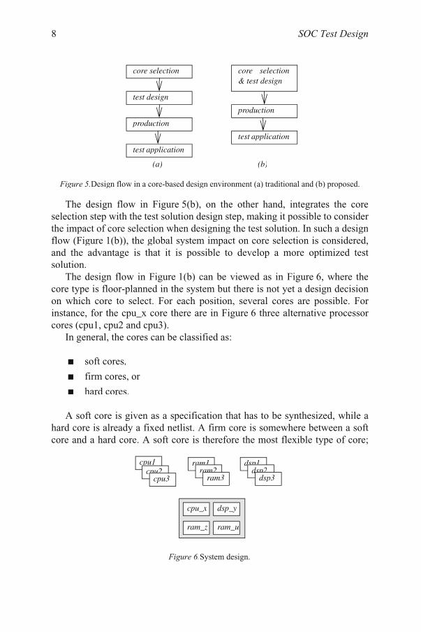
The design flow in Figure 5(b), on the other hand, integrates the coreselection step with the test solution design step, making it possible to considerthe impact of core selection when designing the test solution. In such a designflow (Figure 1(b)), the global system impact on core selection is considered,and the advantage is that it is possible to develop a more optimized testsolution.
The design flow in Figure 1(b) can be viewed as in Figure 6, where thecore type is floor-planned in the system but there is not yet a design decisionon which core to select. For each position, several cores are possible. Forinstance, for the cpu_x core there are in Figure 6 three alternative processorcores (cpu1, cpu2 and cpu3).
In general, the cores can be classified as:
■ soft cores,
■ firm cores, or
■ hard cores.
A soft core is given as a specification that has to be synthesized, while ahard core is already a fixed netlist. A firm core is somewhere between a softcore and a hard core. A soft core is therefore the most flexible type of core;
Figure 5.Design flow in a core-based design environment (a) traditional and (b) proposed.
core selection
production
test application
test design
core selection& test design
production
test application
(a) (b)
Figure 6.System design.
cpu1cpu2
cpu3
ram1ram2
ram3
cpu_x dsp_y
ram_z ram_u
dsp1dsp2
dsp3

Chapter 2: Design Flow 9
however, it requires the tools, effort and time involved in the work of synthe-sizing it to a gate-level netlist. A hard core, on the other hand, is already fixedand ready to be used in the design. Hence, less effort and time are required forthe optimization of the core. The difference between a soft core, firm core,and a hard core is also visible when it comes to testing. For soft core there is ahigher degree of freedom when determine the test method compared to hardcores where the test method and test vectors are more fixed.
3.1 Network-on-Chip
A problem when the SOC designs grow in complexity is that the on-chipinterconnections, such as buses and switches, can not be used anymore due totheir limited scalability. The wires are simply becoming too long. An alterna-tive is to use networks on chip (NOC) [14, 121].
3.2 Platform-Based Design
The design flow must not only take the development of the hardware intoaccount but also the development of software. Systems of today include anincreasing number of programmable devices. The software (operating systemand application programs as well as compilers) must be developed. In order tofix the architecture, the concept of platform-based design has been developed.Sangiovanni-Vincentelli [237] compare it with the PC (personal computer):
■ The X86 instruction set makes it possible to re-use operating systemsand software applications,
■ Busses (ISA, USB, PCI) are specified,
■ ISA interrupt controller handles basic interaction between softwareand hardware,
■ I/O devices, such as keyboard, mouse, audio and video, have a clearspecification.
The PC platform has eased the development for computers. However,most computers are not PCs but embedded systems in mobile phones, cars,etc [266]. Hence, a single platform-based architecture for all computer sys-tems is not likely to be found.

SOC Test Design10
4 CLOCKING
Clocking the system is becoming a challenge. Higher clock frequenciesare making timing issues more important. The storage elements (flip-flopsforming registers) in a system have to be controlled. For instance, Figure 7(a)shows a finite state machine (FSM), and a pipelined system is in Figure 7(b);the storage devices are controlled by the clock. Most systems are a combina-tion of FSM and pipelined systems.
The input of a register (flip-flop) is commonly named D, and the outputnamed Q. Figure 8 illustrates the following:
■ the setup time (TsTT ) - the time required before the edge until the valueis stable at the D input,
■ the hold time (ThTT ) - the time required after the edge in order store thevalue in the register,
■ the clock-to-Q delay (TqTT ) - the time required after the edge in order toproduce the value on Q,
■ the cycle time (TcTT ) - the time between two positive edges (from 0 to1).
The registers can be design for instance as a level-sensitive latch, edge-trigged register, RS latch, T register, and JK register [277].r
Figure 7.Clocked systems. (a) a finite state machine (FSM); (b) a pipelined system.
inputs outputscombinationallogic
DQ
next state bitscurrent state bits
registers
clock
(a)
QDD
clock
inputslogic QDD logic
registers registers
QDD logic
registers
QDD
registersoutputs
(b)

Chapter 2: Design Flow 11
4.1 System Timing
Latches and registers can be used in different ways to implement a clockedsystem [277]. It is important that the clock signal is delivered to the registerscorrectly. Long wires may introduce delays in the clock distribution leadingto clock skew - the clock signal is not delivered at the same time to all clockedelements.
The cycle time (TcTT ) is given by:
where TqTT is the clock-to-Q delay, TsTT is the setup time, and TdTT is the worst-case delay through the combinational logic blocks.
4.2 Clock Distribution
Clock distribution is a problem. For instance, the total capacitance in thesystem that has to be driven can be above 1000 pF [277]. Driving such capac-itance at high repetition rate (clock speed) creates high current (see examplein Figure 9).
Figure 8.Single phase clocking and its parameters.
clock
data
Q
cycle time (Tc)
setup time (Ts)
hold time (Th)
clock-to-Q time(Tq)
Tc Tq Td Ts+ +Td=
Figure 9.Example illustrating high current and power [277].
VDD = 5VCreg = 2000 pF (20K register bits @ .1pFTclk = 10 nsTrise/fall = 1 ns
Ipeak = C×dv/dt = (2000×10-12×5)/(1.0×10-9) = 10APd = Cpp
×Vdd2×f = 2000×10-12×25×100×10-6= 5W

SOC Test Design12
The clock can be distributed using [277]:
■ a single large buffer (i.e. cascaded inverters) that is used to drive allmodules, or
■ a distributed-clock-tree approach (Figure 10).
4.3 Multiple Clock Domains
In a core-based design, a set of cores are integrated to a system. Each coremight require its dedicated clock speed. A design with multiple clockdomains can present challenges. A typical problem is at the clock-domainboarders where one clock frequency is meeting another clock domain. Prob-lems that can appear are, for instance, data loss and metastability. Data losscan appear when data generated by clock1 is not captured by clock2 until ithas already been changed. Such problems appear if the destination clock isrunning at a higher speed. Metastability is due to that there is no timing rela-tion between source and destination clock domain, and it can happen that dataand clock signals reach the flip-flops at the same time. Metastability cancause reliability problems.
4.3.1 Phase Locked Loop (PLL)
A phase locked loop (PLL) is used to generate internal clocks in the sys-tem for two main reasons [277]:
■ Synchronize the internal clock with an external clock.
■ The internal clock should operate at a higher frequency than theexternal clock.
Figure 10.Distributed clock-tree where the logic is omitted.
Register
clockRegister
Register
Register
delays must match

Chapter 2: Design Flow 13
The increasing on-chip clock speed has lead to clock skew problems. APLL allows an internal clock to be generated that is in phase with an externalclock.
4.3.2 Globally-Asynchronous Locally-Synchronous
The advantage of making a system synchronous is that it is:
■ a proven technique, and
■ wide-spread EDA tools are available.
However, it is important to note that
■ clock speed limited by slowest operation,
■ clock distribution a problem,
■ hard to design systems with multiple clock domains, and
■ energy is consumed for idle operation.
An alternative is to make the system asynchronous. Instead of synchronizebased on a clock, the system is controlled through communication protocol(often hand-shaking). The advantages with such a system are that is:
■ ”average-case” performance,
■ no clock signal to distribute, and
■ no energy for idle operations.
The disadvantages with the asynchronous design approach are that:
■ limited EDA supports, and
■ extremely difficult to test.
Chapiro [36] proposed a scheme named Globally-asynchronous locally-synchronous (GALS) where there is an asynchronous wrapper around eachcore/block and where each core itself is synchronous. FIFO queues areinserted at the boundaries between the asynchronous and the synchronousparts.
The advantages with GALS are:
■ easy to design systems with multiple clock domains,
■ no global clock to distribute,
![References - link.springer.com978-3-662-04616-6/1.pdf · References [AB95] Andreae, T., Bandelt, H.-J.: Performance guarantees for approximation al gorithms depending on parameterized](https://static.fdocuments.in/doc/165x107/5f93149f58a649093945a542/references-link-978-3-662-04616-61pdf-references-ab95-andreae-t-bandelt.jpg)


![Benchmarking Separable Natural Evolution Strategies on the …people.idsia.ch/~tom/publications/bbob-snes.pdf · 2012-06-05 · Algorithms and Problem Complexity]: Numerical Al-gorithms](https://static.fdocuments.in/doc/165x107/5f1a45c3b0e99923b13f2c85/benchmarking-separable-natural-evolution-strategies-on-the-tompublicationsbbob-snespdf.jpg)

![Separating Reflective and Fluorescent Components of an Imageresearch.nii.ac.jp/~imarik/resources/papers/CVPR... · separating components of an image [14, 17]. Some al-gorithms separate](https://static.fdocuments.in/doc/165x107/604408327146ee587959a7b6/separating-reiective-and-fluorescent-components-of-an-imarikresourcespaperscvpr.jpg)