Introduction - National Technology & Science Press · This module was written as an introduction to...
17
1 1 CHAPTER Introduction With the development of the integrated circuit, the semiconductor industry is undoubtedly the most influential industry to appear in our society. Its impact on almost every person in the world exceeds that of any other industry since the beginning of the Industrial Revolution. The reasons for its success are as follows: ◆ Exponential growth of the number of functions on a single integrated circuit. ◆ Exponential reduction in the cost per function. ◆ Exponential growth in sales (economic impor- tance) for approximately forty years. This growth has led to ever-increasing perfor- mance at lower prices for consumer electronics such as cellular phones, personal computers, audio play- ers, etc. The computational power available to the individual has increased to the point that it has changed the way we think about problem solving. Communication technology including wired and wireless networks have fundamentally changed the way we live and communicate. The innovation responsible for these impressive results is the integration of electronic circuit compo- nents fabricated in silicon integrated circuit (IC) technology. Today, many of the ICs shaping new applications contain both analog and digital cir- cuitry, and are therefore called mixed-signal inte- grated circuits. In mixed-signal ICs, the analog circuitry is typically responsible for interfacing with physical signals, and concerned for example with the amplification of a weak signal from an antenna, or driving a sound signal into a loudspeaker. On the other hand, digital circuitry is primarily used for computing, enabling powerful functions such as Fast Fourier Transforms or floating point multiplication. This module was written as an introduction to the analysis and design of analog integrated circuits in complementary metal-oxide-semiconductor (CMOS) technology. In this first chapter, we will motivate this subject by looking at an example of a mixed-signal IC and by highlighting the need for a systematic study of the fundamental principles and proper engineering approximations in analog design. Chapter Objectives ◆ Provide a motivation for the study of elementary analog integrated circuits.
-
Upload
truongmien -
Category
Documents
-
view
217 -
download
0
Transcript of Introduction - National Technology & Science Press · This module was written as an introduction to...

1
1C H A P T E R
Introduction
With the development of the integrated circuit, thesemiconductor industry is undoubtedly the mostinfluential industry to appear in our society. Itsimpact on almost every person in the world exceedsthat of any other industry since the beginning of theIndustrial Revolution. The reasons for its success areas follows:
◆ Exponential growth of the number of functionson a single integrated circuit.
◆ Exponential reduction in the cost per function.
◆ Exponential growth in sales (economic impor-tance) for approximately forty years.
This growth has led to ever-increasing perfor-mance at lower prices for consumer electronics suchas cellular phones, personal computers, audio play-ers, etc. The computational power available to theindividual has increased to the point that it haschanged the way we think about problem solving.Communication technology including wired andwireless networks have fundamentally changed theway we live and communicate.
The innovation responsible for these impressiveresults is the integration of electronic circuit compo-nents fabricated in silicon integrated circuit (IC)technology. Today, many of the ICs shaping new
applications contain both analog and digital cir-cuitry, and are therefore called mixed-signal inte-grated circuits. In mixed-signal ICs, the analogcircuitry is typically responsible for interfacing withphysical signals, and concerned for example with theamplification of a weak signal from an antenna, ordriving a sound signal into a loudspeaker. On theother hand, digital circuitry is primarily used forcomputing, enabling powerful functions such as FastFourier Transforms or floating point multiplication.
This module was written as an introduction to theanalysis and design of analog integrated circuits incomplementary metal-oxide-semiconductor(CMOS) technology. In this first chapter, we willmotivate this subject by looking at an example of amixed-signal IC and by highlighting the need for asystematic study of the fundamental principles andproper engineering approximations in analogdesign.
Chapter Objectives
◆ Provide a motivation for the study of elementaryanalog integrated circuits.
2 Chapter 1 Introduction
◆ Provide a roadmap for the subjects that will becovered throughout this module.
◆ Review fundamental concepts for the construc-tion of two-port circuit models.
1-1 Mixed-Signal Integrated Circuits
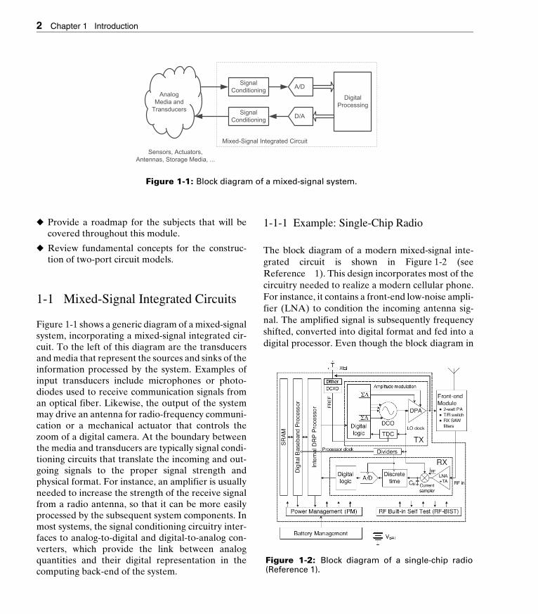
Figure 1-1 shows a generic diagram of a mixed-signalsystem, incorporating a mixed-signal integrated cir-cuit. To the left of this diagram are the transducersand media that represent the sources and sinks of theinformation processed by the system. Examples ofinput transducers include microphones or photo-diodes used to receive communication signals froman optical fiber. Likewise, the output of the systemmay drive an antenna for radio-frequency communi-cation or a mechanical actuator that controls thezoom of a digital camera. At the boundary betweenthe media and transducers are typically signal condi-tioning circuits that translate the incoming and out-going signals to the proper signal strength andphysical format. For instance, an amplifier is usuallyneeded to increase the strength of the receive signalfrom a radio antenna, so that it can be more easilyprocessed by the subsequent system components. Inmost systems, the signal conditioning circuitry inter-faces to analog-to-digital and digital-to-analog con-verters, which provide the link between analogquantities and their digital representation in thecomputing back-end of the system.
1-1-1 Example: Single-Chip Radio
The block diagram of a modern mixed-signal inte-grated circuit is shown in Figure 1-2 (seeReference 1). This design incorporates most of thecircuitry needed to realize a modern cellular phone.For instance, it contains a front-end low-noise ampli-fier (LNA) to condition the incoming antenna sig-nal. The amplified signal is subsequently frequencyshifted, converted into digital format and fed into adigital processor. Even though the block diagram in
DigitalProcessing
A/D
D/A
SignalConditioning
SignalConditioning
AnalogMedia and
Transducers
Sensors, Actuators,Antennas, Storage Media, ...
Mixed-Signal Integrated Circuit
Figure 1-1: Block diagram of a mixed-signal system.
Figure 1-2: Block diagram of a single-chip radio(Reference 1).

Section 1-1 Mixed-Signal Integrated Circuits 3
Figure 1-2 looks quite complex, all of its elementscan be mapped into one of the blocks of the genericdiagram of Figure 1-1.
Figure 1-3 shows the chip photo of the single-chipradio, with some of the system’s key building blocksannotated. As evident from this diagram, the digitallogic dominates the area of this particular IC. Thissituation is not uncommon in modern mixed-signalICs, not least because the utilized digital algorithmshave reached an enormous complexity, requiringmillions or tens of millions of logic gates.
Despite the dominance of digital logic withinmost systems, the analog interface components areequally important, as they determine how and howmuch information can be communicated betweenthe physical world and the digital processing back-bone. In many cases, the performance of the signalconditioning and data conversion circuitry ulti-mately determines the performance of the overallsystem.
1-1-2 Example: Photodiode Interface Circuit
Figure 1-4 shows an example of a signal conditioningcircuit that plays a critical role in fiber-optic commu-nication systems. In such a system, a photodiode is
used to convert light intensity to electrical current(iIN). In order to condition the signal for further pro-cessing, the diode current is converted into a voltage(vOUT) by a so-called transimpedance amplifier. Thisamplifier must be fast enough to process the incom-ing light pulses, which often occur at frequencies ofmultiple gigahertz. In addition, the amplifier mustobey certain limits on power dissipation, or the sys-tem may become impractical in terms of heat man-agement or power supply requirements.
Limitations in speed and power dissipation are, ingeneral, among the main concerns in the interfacecircuitry of mixed-signal systems. Since new prod-ucts tend to demand higher performance, the analogdesigner is constantly concerned with the design andoptimization of system-critical building blocks, aim-ing for the best possible performance that can beachieved within the framework of the target applica-tion and process technology.
A specific example for the circuit realization of atransimpedance amplifier is shown in Figure 1-5. Itconsists of three transistor stages, each of whichserves a specific purpose and design intent. This istrue for most amplifier circuits; even though the fullschematic of a particular realization may be com-plex, it can usually be broken up into smallersub-blocks that are more easily understood. Specifi-cally, for the amplifier of Figure 1-5, the experienceddesigner will recognize that the circuit consists of acascade connection of a common-gate, com-mon-source, and common-drain stage. Thesesub-blocks form the basis for a large number of ana-log circuits, and can be viewed as the “atoms” or fun-damental building blocks of analog design. In thismodule, you will learn to analyze these blocks fromfirst principles, and to reuse the gained knowledgefor the design of more complex circuits. The circuit
Figure 1-3: Chip photo of a single-chip radio(Reference 1).
iINvOUT
TransimpedanceAmplifier
Optical Fiber
Figure 1-4: Photodetector circuit for fiber-opticcommunication.

4 Chapter 1 Introduction
of Figure 1-5 will be analyzed in detail in Chapter 6of this module, building upon the principles coveredin Chapters 2–5.
1-2 Managing Complexity
As evident from the example of Section 1-1-1, mod-ern integrated circuits are highly complex andrequire a hierarchical approach in design and analy-sis. That is, a modern integrated circuit is far toocomplex to be fully understood and analyzed in asingle sheet schematic at the transistor level. Typi-cally, a mixed-signal IC is represented by a block dia-
gram as the one shown in Figure 1-2. At the level ofthis description, suitable specifications are derivedfor each block, which may itself contain severalsub-blocks. The blocks and sub-blocks are thendesigned and optimized until they meet the desiredtarget specifications.
Figure 1-6 illustrates examples of the various lev-els of abstraction that come into play in the design ofa modern integrated circuit. At the highest level, theconstituent elements can be partitioned into analogand digital blocks. An example of a high-level analogblock is an analog-to-digital converter, whereas amicroprocessor is an example of a large digital block.These blocks themselves contain smaller functionalunits, as, for example, operational amplifiers in thecase of an analog-to-digital converter. The opera-tional amplifiers themselves contain the aforemen-tioned elementary transistor stages, which are themain subject of this module.
Interestingly, even at the level of elementary tran-sistor stages, is often not possible to work with a per-fect model or description of the circuit. This isparticularly so because the physical effects in theconstituent transistors are highly complex and oftenimpossible to capture perfectly with a tractable set ofequations for hand analysis. Therefore, makingproper engineering approximations in transistormodeling is an important aspect in maintaining a sys-tematic design methodology. For this particular rea-son, the presentation in this module follows a“just-in-time” approach for the modeling of transis-tor behavior. Rather than deriving a complete
iinIB1
vOUT
Common-GateStage
Common-SourceStage
Common-DrainStage
Figure 1-5: Example realization of a transim-pedance amplifier.
Device Physics
Device Modeling
Elementary Transistor Stages Logic Gates
Operational Amplifiers Arithmetic Blocks
Filters, Data Converters Microprocessors
Mixed-Signal Systems
Digital Analog
Figure 1-6: Levels of abstraction in integrated circuit design.

Section 1-3 Two-Port Abstraction for Amplifiers 5
transistor model in an isolated chapter (as done inmost texts), we begin with only the basic deviceproperties and increase complexity throughout themodule upon demand, and where needed to gainfurther insight and accuracy. With this approach, thereader learns to appreciate the complexity of arefined model, and will be able to assess and trackpotential limitations of working with simplifiedmodels.
1-3 Two-Port Abstraction for Amplifiers
High-level system block diagrams, such asFigure 1-2, are typically drawn as unidirectionalflowcharts and do not capture details about the elec-trical behavior of each connection port and how cer-tain blocks may interact once they are connected.Unfortunately, electrical signals are not unidirec-tional, and connecting two blocks always means thatthere is some level of interaction through the volt-ages and currents at the connection points.
The commonly used linear two-port modelingabstraction for amplifiers and amplifier stages allowsthe designer to take these effects into account whilemaintaining a high level of abstraction. For instance,the circuit of Figure 1-5 can be approximately mod-eled as shown in Figure 1-7 (the details on obtainingthis model are discussed later in this module). Eachstage of the overall amplifier is represented via asimplified circuit model that captures its essentialfeatures. Once this model is created, the interactionamong stages can be analyzed at this high level ofabstraction, without requiring detailed insight on
how each stage is implemented. The two-port mod-eling approach is particularly useful in the design ofamplifiers, as it can help shape the thought processon how the various stages should be configured tooptimize performance. In the following subsections,we will review some of the basic concepts of ampli-fier two-port modeling used in this module.
1-3-1 Amplifier Types
In this module, we model amplifier circuits as blocksthat have an input and output port, where the term“port” refers to a pair of terminals. For each port, wecan define input and output currents and voltages asshown in Figure 1-8. Depending on the intendedfunction, we distinguish between the four possibleamplifier types listed in Table 1-1. For example, anamplifier that takes an input current and amplifiesthis current to produce a proportional output volt-age is called a transresistance amplifier. In this con-text, it is important to emphasize that in a generalpractical amplifier circuit, the input and output portswill always carry both nonzero voltages and currents,and there exist transfer functions between all
Rout1
Ai1·iin
Rin1
iin vin2
Rout2
Gm2·vin2
vin3
Av3·vin3
Rout3
+vout−
+−
Figure 1-7: Two-port model of the transimpedance amplifier circuit inFigure 1-5.
Amplifier
iin iout
vin vout
Figure 1-8: General amplifier two-port.

6 Chapter 1 Introduction
possible combinations of input/output variables.What truly defines the type of an amplifier is whatthe circuit designer deems as the main quantities ofinterest in the amplifier’s application.
Now, in order to model the inner workings ofeach amplifier type, we can invoke the four corre-sponding two-port amplifier models shown inFigure 1-9. Each amplifier model has an input andoutput resistance (or more generally, a frequencydependent impedance) and a controlled source tomodel the amplification.
◆ In the voltage amplifier model, the controlledsource is a voltage-controlled voltage source. Ide-ally, the input resistance is infinite (open circuit,no current flow). The ideal output resistance iszero (ideal voltage source).
◆ The current amplifier model has a current-con-trolled current source. Ideally, the input resis-tance is zero (short circuit, no voltage across theinput port) and the output resistance is infinite(ideal current source).
◆ The transconductance amplifier model has a volt-age-controlled current source. Ideally, the inputresistance is infinite (open circuit, no currentflow). The ideal output resistance is also infinite(ideal current source).
◆ The transresistance or transimpedance1 amplifiermodel has a current-controlled voltage source.Ideally, the input resistance is zero (short circuit,no voltage across the input port). The ideal out-put resistance is also zero (ideal voltage source).
From these four models and their ideal behavior,we note that the two-ports containing a voltage-con-trolled source should ideally have large input resis-tance (Rin). This minimizes the signal loss due toresistive voltage division between the source voltage(vs) and the control voltage (vin). In contrast, thetwo-ports that use a current-controlled sourceshould have small input resistance to minimize thesignal loss due to current division between thesource current (is) and the control current (iin). Inthis context, “large” and “small” refer to the value ofRin relative to the source resistance (Rs).
On the output side, if the variable of interest is avoltage, the output resistance (Rout) should be smallso that only a small amount of the amplified voltage
Table 1-1: Amplifier types.
Amplifier Type Input Quantity
Output Quantity
Voltage Amplifier Voltage Voltage
Current Amplifier Current Current
Transconductance Amplifier Voltage Current
Transresistance Amplifier Current Voltage
1. The term transimpedance is sometimes used to refer to an ampli-fier that is primarily meant to realize a transresistance. Referring to“impedance” highlights the fact that the transfer function will usual-ly be frequency-dependent.
Figure 1-9: Two-port amplifier models with inputsource and load: (a) voltage amplifier, (b) currentamplifier, (c) transconductance amplifier, and (d)transresistance amplifier.

Section 1-3 Two-Port Abstraction for Amplifiers 7
is lost through the division with the load (RL). Con-versely, for a current output, the output resistanceshould be large to minimize current division losses.Again, “large” and “small” are taken as relativemeasures comparing Rout to RL.
Consider for example the voltage amplifier ofFigure 1-9(a). To calculate the transfer function ofthe overall circuit (vout/vs), the input voltage, includ-ing its source resistance, is connected to the input ofthe two-port model and the load resistance is con-nected to the output. The full circuit is shown inFigure 1-10.
Applying the voltage divider rule at the input andoutput of the circuit gives
(1.1)
As we can see from this expression, the overallvoltage gain is maximized when the amplifier has alarge input resistance (relative to Rs) and a small out-put resistance (relative to RL). For the ideal case ofinfinite input resistance and zero output resistance,vout/vs becomes equal to Av.
For the sake of compact notation, we will oftenwant to use a symbol for the overall circuit gain. Thenotation used in this module uses primed variablesto distinguish between the gain of the controlledsource and the gain of the overall amplifier circuit.For example, for the above-discussed voltage ampli-fier we define . This notation is meantto emphasize the connection between the two sym-bols. is usually smaller than Av, but can approachAv for ideal source and load configurations.
Example 1-1: Transfer Function of aTransconductance Amplifier.
For the transconductance amplifier circuit in FigureEx1-1, calculate the overall transconductance
.
vx
Figure 1-10: Voltage amplifier with connected source and loadresistances.
voutvs
--------vinvs------⎝ ⎠
⎛ ⎞ Avvoutvx
--------⎝ ⎠⎛ ⎞⋅ ⋅=
RinRin Rs+-------------------⎝ ⎠
⎛ ⎞ AvRL
RL Rout+----------------------⎝ ⎠
⎛ ⎞⋅ ⋅=
A′v vout vs⁄=
A′v
ix
Figure Ex1-1
G′m iout vs⁄=

8 Chapter 1 Introduction
SOLUTION
Applying the voltage divider rule at the input andthe current divider rule at the output yields the fol-lowing result:
Thus, the overall transconductance gain is maxi-mized when the amplifier has a large input resistance(relative to Rs) and a large output resistance (rela-tive to RL). For the ideal case of infinite input andoutput resistances, becomes equal to Gm.
As a final remark for this sub-section, it is impor-tant to recognize that all of the models in Figure 1-9can be used interchangeability to describe the exactsame electrical behavior (see Problem P1-1). Forinstance, a voltage amplifier model can be convertedinto a transconductance amplifier model by applyinga Thevénin to Norton transformation for the con-trolled source.
A corollary to this equivalence is that we can forexample use a transconductance amplifier model todescribe a voltage amplifier circuit. This is illustratedthrough the circuit of Figure 1-10, which is electri-cally equivalent to that of Figure 1-10 (seeProblem P1-2). Note that the output is taken as thevoltage across the output port instead of the outputcurrent; this indicates that the circuit is viewed as a
voltage amplifier. Just as in the original circuit ofFigure 1-10, we require a large input resistance andsmall output resistance for this circuit to maximizethe overall voltage gain.
The choice of amplifier model depends on severalfactors. At first glance, it seems natural to modeleach amplifier type using its “native” model thatdirectly corresponds to the intended function. Forexample, we could always describe a voltage ampli-fier using the corresponding voltage amplifier modelthat contains a voltage controlled voltage source.However, as we shall see throughout this module, itis sometimes more convenient to align the amplifiermodel with the physical amplification mechanism ora structural feature of the underlying transistor cir-cuit. For instance, the common-source voltageamplifier discussed in Chapter 2 naturally invokes atransconductance-based model due to the physicalmodel of the employed transistor.
1-3-2 Unilateral versus Bilateral Two-Ports
All of the two-port models shown in Figure 1-9 arecalled unilateral, because they can only propagate asignal from the input port to the output port and notthe other way around. For instance, injecting a cur-rent into the output port of the current amplifier ofFigure 1-9(b) will not induce a current at the inputport. Unfortunately, many practical transistor cir-cuits are not unilateral, and exhibit bilateral behav-ior when analyzed in detail, and especially at highfrequencies.
G′ mioutvs
-------vinvs------⎝ ⎠
⎛ ⎞ Gmioutix
-------⎝ ⎠⎛ ⎞⋅ ⋅= =
RinRin Rs+-------------------⎝ ⎠
⎛ ⎞ GmRL
RL Rout+----------------------⎝ ⎠
⎛ ⎞⋅ ⋅=
G′m
Gm = -Av/Rout
Figure 1-11: Voltage amplifier with an underlyingtransconductance amplifier model.

Section 1-3 Two-Port Abstraction for Amplifiers 9
An example of a bilateral current amplifier isshown Figure 1-12(a). Note that in this circuit, resis-tor R2 couples the input and output networks and itcan therefore transfer currents in both directions.Consequently, the unilateral model of Figure 1-9(b)cannot perfectly represent this circuit. When it isdesired to capture the bilateral behavior, thetwo-port model in Figure 1-12(b) could be employedin principle. Here, the controlled source Air modelsthe reverse current transfer from the output back tothe input. Alternatively, one could employ otherbilateral and more general two-port models basedon admittance parameters (Y), impedance parame-ters (Z), and hybrid or inverse-hybrid parameters (Hor G); see advanced circuit design texts such as Ref-erence 2. These models are particularly useful whenreverse transmission (i.e., feedback from the outputto the input) is incorporated in the circuit as part ofthe intended design.
There are two reasons why we will work exclu-sively with unilateral two-port approximations inthis module. First, the circuits considered are
designed primarily to implement forward gain ratherthan reverse gain; feedback circuits are not treatedin this module. For example, referring to the modelof Figure 1-12(b), the reverse gain Air will be negligi-bly small in any current amplifier circuit that we willconsider. Second, a clear drawback of working withbilateral two-port models would be a significantincrease in analysis complexity. As we have seen inExample 1-1, the overall transfer function of a uni-lateral two-port circuit can be written by applyingsimple voltage and current divider rules. This alsoextends to cascade connections of multipletwo-ports. For example, the overall transfer functionof the circuit in Figure 1-7 is easily written by inspec-tion, without requiring extensive algebra. Withreverse transmission included, the transfer functionanalysis will generally require solving a linear systemof equations. In light of the fact that we do not intendto design circuits in this module that have significantreverse transmission, this increase in complexity isnot welcome, and would also hinder us from devel-oping intuition from inspection-driven analysis.
1-3-3 Construction of Unilateral Two-Port Models
We will now describe the general procedures to cal-culate the controlled sources, as well as the input andoutput resistances, for the unilateral two-port mod-els of Figure 1-9. The approach is based on applyingtest voltages and currents to find the desired modelparameters.
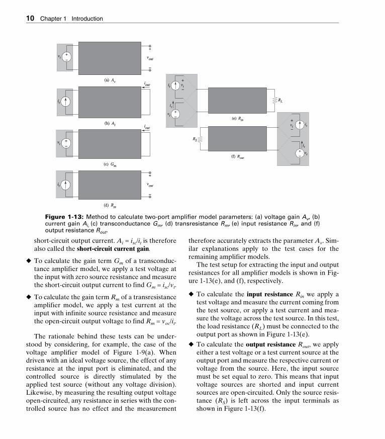
The most important parameter of any amplifiercircuit is its gain. To identify the gain parameters forthe models of Figure 1-9(a)-(d), we apply the testsshown in Figure 1-13(a)-(d), respectively.
◆ To calculate the gain term Av of a voltage ampli-fier model, we apply a test voltage at the inputwith zero source resistance and measure theopen-circuit output voltage. Av = voc/vt is there-fore also called the open-circuit voltage gain.
◆ To calculate the gain term Ai of a current ampli-fier model, we apply a test current at the inputwith infinite source resistance and measure the
(a)
(b)
gm·vin
+vin-
R2
R1
iin iout
Aif·iin
iin iout
Rout
Air·iout
Rin
Figure 1-12: (a) Example of a bilateral currentamplifier. (b) Corresponding bilateral currentamplifier two-port model.
10 Chapter 1 Introduction
short-circuit output current. Ai = isc/it is thereforealso called the short-circuit current gain.
◆ To calculate the gain term Gm of a transconduc-tance amplifier model, we apply a test voltage atthe input with zero source resistance and measurethe short-circuit output current to find Gm = isc/vt.
◆ To calculate the gain term Rm of a transresistanceamplifier model, we apply a test current at theinput with infinite source resistance and measurethe open-circuit output voltage to find Rm = voc/it.
The rationale behind these tests can be under-stood by considering, for example, the case of thevoltage amplifier model of Figure 1-9(a). Whendriven with an ideal voltage source, the effect of anyresistance at the input port is eliminated, and thecontrolled source is directly stimulated by theapplied test source (without any voltage division).Likewise, by measuring the resulting output voltageopen-circuited, any resistance in series with the con-trolled source has no effect and the measurement
therefore accurately extracts the parameter Av. Sim-ilar explanations apply to the test cases for theremaining amplifier models.
The test setup for extracting the input and outputresistances for all amplifier models is shown in Fig-ure 1-13(e), and (f), respectively.
◆ To calculate the input resistance Rin we apply atest voltage and measure the current coming fromthe test source, or apply a test current and mea-sure the voltage across the test source. In this test,the load resistance (RL) must be connected to theoutput port as shown in Figure 1-13(e).
◆ To calculate the output resistance Rout, we applyeither a test voltage or a test current source at theoutput port and measure the respective current orvoltage from the source. Here, the input sourcemust be set equal to zero. This means that inputvoltage sources are shorted and input currentsources are open-circuited. Only the source resis-tance (RS) is left across the input terminals asshown in Figure 1-13(f).
Figure 1-13: Method to calculate two-port amplifier model parameters: (a) voltage gain Av, (b)current gain Ai, (c) transconductance Gm, (d) transresistance Rm, (e) input resistance Rin, and (f)output resistance Rout.

Section 1-3 Two-Port Abstraction for Amplifiers 11
The above procedures extract the input and out-put resistances perfectly and without any approxi-mations, even if the circuit is bilateral. As we shallsee through the examples below, Rin and Rout do notdepend on RL and RS, respectively, in a perfectly uni-lateral amplifier. However, this is not the case in abilateral amplifier, and therefore the general proce-dure includes RL and RS in the test setup.
In summary, the above procedures for measuringunilateral two-port model parameters aim at findingthe best possible unilateral representation of an arbi-trary amplifier circuit, which itself may or may not beunilateral. The obtained models are approximatewhen the amplifier is bilateral, since they do notinclude a controlled source that captures reversetransmission from the output back to the input. Inmost cases considered in this module, the reversetransmission term is negligible. Exceptions will behighlighted and treated as appropriate.
Example 1-2: Two-Port Model Calculationsfor a Unilateral Amplifier
For the transconductance amplifier in FigureEx1-2A, calculate the following two-port modelparameters: the transconductance Gm, the inputresistance Rin, and the output resistance Rout. Also,compute the overall transfer function .
SOLUTION
To find the transconductance, we short the outputport and apply an ideal test voltage source (vt) at theinput [see Figure Ex1-2B(a)]. From this circuit, wesee that
Next, to find Rin, we apply a test voltage at theinput and connect the load resistance RL at the out-put [Figure Ex1-2B(b)]. From this circuit, we findthat the input resistance is simply the series connec-
R3
gm·vx
R2
+
vin
-
ioutvx
R1R4
RL
RS
vS
Figure Ex1-2A
G′m iout vs⁄=
R3
gm·vx
R2
iscvx
R1R4
vt
R3
gm·vx
R2
ioutvx
R1R4
vt
RL
it
R3
gm·vx
R2
itvx
R1R4
RS
vt
(a)
(b)
(c)
Figure Ex1-2B
Gmiscvt-----
gmvxR3
R3 R4+------------------⋅
vt----------------------------------
gmvtR2
R1 R2+------------------
R3
R3 R4+------------------⋅ ⋅
vt----------------------------------------------------------= = =
gmR2
R1 R2+------------------
R3
R3 R4+------------------⋅ ⋅=

12 Chapter 1 Introduction
tion of R1 and R2, i.e., Rin = R1 + R2. Note that theoutput network does not influence this result.
Finally, to find Rout, we apply a test voltage at theoutput and connect the source resistance RS acrossthe input port (the source vs is replaced by a short),[see Figure Ex1-2B(c)]. In the resulting circuit, vxmust be zero, because no current is flowing in theinput network. Thus, the controlled source carriesno current and we conclude that Rout = R3 + R4.
In order to compute the transfer function of thecomplete circuit, we can reuse the result obtained inExample 1-1.
Substituting Gm, Rin, and Rout from the above calcu-lation yields the final result.
In the preceding example, we have seen that thesource and load resistances have no effect on theextracted two-port parameters. In the followingexample, we will investigate a bilateral circuit toshow that in general, the input and output resis-tances depend on RS and RL, which must thereforealways be included in the general two-port modelingcalculations.
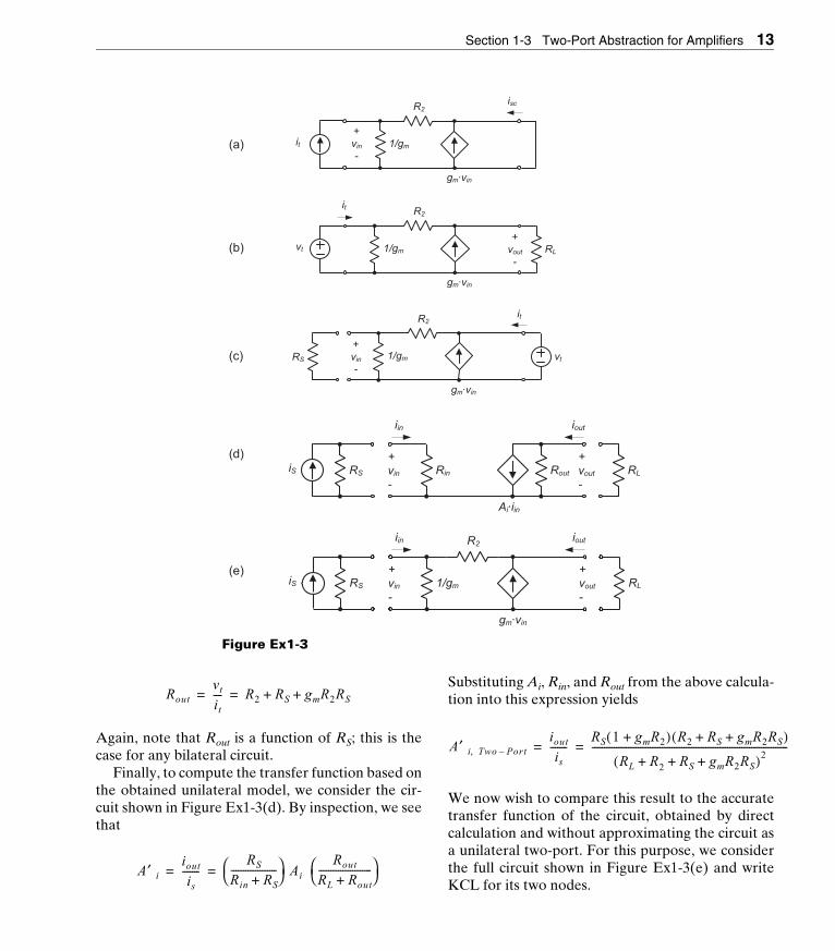
Example 1-3: Two-Port Model Calculationsfor a Bilateral Amplifier
For the current amplifier in Figure 1-12(a), calculatethe following unilateral two-port model parameters:the current gain Ai, the input resistance Rin, and theoutput resistance Rout. Also, compute the overalltransfer function iout/vs using the obtained unilateraltwo-port model. Compare the result to a directKCL-based analysis of the transfer function.Assume that the circuit is driven by a current sourcewith resistance RS and loaded by a resistance RL. Foralgebraic simplicity, assume R1 = 1/gm (this case cor-responds to the common-gate amplifier circuit cov-ered in Chapter 4).
SOLUTION
To find the current gain Ai, we short the output portand apply an ideal test current source (it) at the input[see Figure Ex1-3(a)]. From this circuit, we see that
and
Thus, Ai = isc/it = –1.Next, to find Rin, we apply a test voltage at the
input and connect the load resistance RL at the out-put [Figure Ex1-3(b)]. From this circuit, we note thatthe input resistance is not easily identified by inspec-tion. Hence we write KCL for the two nodes of thecircuit (vt and vout).
Solving this system of equations yields
Note from this result that Rin depends on RL, as men-tioned previously; this dependency stems from thebilateral structure of the circuit. Also note that Rinapproaches 1/gm when R2 is large compared to RLand 1/gm. We will revisit this important point inChapter 4, in the context of a common-gate ampli-fier circuit.
Now, to find Rout, we apply a test voltage at theoutput and connect the source resistance RS acrossthe input port [Figure Ex1-3(c)]. Again, we mustwrite KCL at the two circuit nodes and solve theresulting system of equations. This yields
G′ mioutvs
-------Rin
Rin RS+-------------------⎝ ⎠
⎛ ⎞ Gm Rout
RL Rout+----------------------⎝ ⎠
⎛ ⎞= =
G′ mioutvs
-------gmR2R3
R1 R2 RS+ +( ) RL R3 R4+ +( )-----------------------------------------------------------------------= =
vin gm1R2
-----+⎝ ⎠⎛ ⎞ 1–
it⋅=
isc gm1R2
-----+⎝ ⎠⎛ ⎞– vin⋅=
0 it– gmvtvt vout–R2
------------------+ +=
0 g– mvtvoutRL--------
vout vt–R2
------------------+ +=
Rinvtit----
R2 RL+1 gmR2+---------------------
1RLR2
------+
gm1R2
-----+------------------= = =
Section 1-3 Two-Port Abstraction for Amplifiers 13
Again, note that Rout is a function of RS; this is thecase for any bilateral circuit.
Finally, to compute the transfer function based onthe obtained unilateral model, we consider the cir-cuit shown in Figure Ex1-3(d). By inspection, we seethat
Substituting Ai, Rin, and Rout from the above calcula-tion into this expression yields
We now wish to compare this result to the accuratetransfer function of the circuit, obtained by directcalculation and without approximating the circuit asa unilateral two-port. For this purpose, we considerthe full circuit shown in Figure Ex1-3(e) and writeKCL for its two nodes.
gm·vin
isc
it
R2
+vin-
1/gm
gm·vin
vt
R2it
RL1/gm
+vout-
gm·vin
it
vt
R2
+vin-
1/gmRS
(a)
(b)
(c)
(d)
(e)
Ai·iin
+vin-
RLiS+vout-
Rin
iin iout
RS Rout
gm·vin
+vin-
RLiS
R2
+vout-
1/gm
iin iout
RS
Figure Ex1-3
Routvtit---- R2 RS gmR2RS+ += =
A′ iioutis
-------RS
Rin RS+-------------------⎝ ⎠
⎛ ⎞ Ai Rout
RL Rout+----------------------⎝ ⎠
⎛ ⎞= =
A′ i Two, Port–ioutis
-------RS 1 gmR2+( ) R2 RS gmR2RS+ +( )
RL R+ 2 RS gmR2RS+ +( )2---------------------------------------------------------------------------------= =

14 Chapter 1 Introduction
Solving this system of equations for vout and substi-tuting iout = -vout/RL yields
The discrepancy factor between the two results isgiven by
From this result, we see that the discrepancy factorapproaches unity (no error) when R2 is much largerthan RL, a condition that is often satisfied in practice(the ideal load for a current amplifier is a short cir-cuit). In this case, the unilateral two-port model willaccurately describe the behavior of the circuit.
The outcome of the above example captures themain spirit in which we justify relying on unilateraltwo-port models in this module. Even though theconsidered amplifier is strictly speaking bilateral, aunilateral model describes its behavior to within thedesired engineering accuracy, provided that reason-able boundary conditions hold.
1-4 Integrated Circuit Design versus Printed Circuit Board Design
In the design of analog circuits, the underlying tech-nology has a significant impact on the choice ofarchitecture, because it tends to restrict the availabil-
ity and specification range of the underlying activeand passive components. For instance, a designerworking with discrete components on a printed cir-cuit board may be subjected to the following con-straints:
◆ Limit the component count below 100 elementsto achieve a small board area.
◆ Resistors can be chosen in the range of 1Ω–10MΩ.
◆ Capacitors can be chosen in the range of 1pF–10,000 μF.
◆ The resistor and capacitor values match to within1–10%.
◆ The available (discrete) bipolar junction transis-tors match to within 20% in their critical parame-ters.
In contrast, the designer of a CMOS system-on-chipmay face the constraints summarized below:
◆ Avoid using resistors; use as many MOSFETtransistors as needed (within reasonable limits, onthe order of hundreds to several thousands) torealize the best possible circuit implementation.
◆ Capacitors can be chosen in the range of 10fF–100 pF.
◆ The critical parameters in the MOSFET transis-tors can be made to match to within 1%, but varyby more than 30% for different fabrication runs.
◆ Capacitors of similar size can match to within0.1%, but vary by more than 10% for differentfabrication runs.
As a consequence of the vastly different constraintsthat apply to the design of analog circuits in CMOStechnology, the resulting practical and preferred cir-cuit architectures differ substantially from the onesthat would be used in a printed circuit board design.For example, a discrete voltage amplifier may utilizelarge AC coupling capacitors to simplify and decou-ple the biasing of the individual gain stages (see
0 is– gmvinvinRS------
vin vout–
R2
---------------------+ + +=
0 g– mvinvoutRL--------
vout vin–
R2
---------------------+ +=
A′ i Exact,ioutis
-------RS 1 gmR2+( )
RL R+ 2 RS gmR2RS+ +-------------------------------------------------------= =
A′ i Two, Port–
A′ i Exact,-------------------------------
R2 RS gmR2RS+ +RL R+ 2 RS gmR2RS+ +-------------------------------------------------------=
1 RS1R2
----- gm+⎝ ⎠⎛ ⎞+
1RLR2
------+ RS1R2
----- gm+⎝ ⎠⎛ ⎞+
----------------------------------------------------=

Section 1-5 Notation 15
example in Figure 1-14). In contrast, it is typicallynot possible to use AC coupling techniques (exceptfor very high-frequency designs) in integrated cir-cuits, primarily due to the restriction on maximumcapacitor size.
The material covered in this module is primarilyconcerned with analog integrated circuit design.While this choice does not affect many of the keyprinciples used in the analysis and the discussed cir-cuits, it does affect the architectural choices made inarriving at a practical design. For instance, large ACcoupling capacitors are not used throughout the dis-cussion. Also, where appropriate, we will invoke cer-tain assumptions about the typical matching ofcomponent parameters in CMOS to eliminateimpractical design choices.
1-5 Prerequisites and Advanced Material
The reader of this module is expected to be familiar withthe basis concepts of linear circuit analysis (see Refer-ence 3), including
◆ Passive components (resistors, capacitors)
◆ Kirchhoff’s voltage and current laws (KVL andKCL)
◆ Independent and dependent voltage and currentsources; Thevénin and Norton representation ofcontrolled sources
◆ Two-port representation of circuits; calculation ofport resistances and frequency dependent imped-ances
◆ Manipulation of complex variables and numbers
◆ Phasor analysis and Laplace domain representa-tion of passive circuit elements
◆ Bode plots
The derivations of device models in this moduleassume familiarity with basic solid-state physics andelectrostatics as treated in introductory texts onsolid-state device physics (see Reference 4).
A few sections of this module are marked with anasterisk (*) to indicate advanced material that mayin some cases go beyond the learning goals of anintroductory course. These sections can be skippedat the instructor’s discretion without affecting theoverall flow and context.
1-6 NotationThis module follows the notation for signal variablesas standardized by the IEEE. Total signals are com-posed of the sum of DC quantities and small signals.For example, a total input voltage vIN is the sum of aDC input voltage VIN and a small-signal voltage vin.The notation is summarized below.
◆ Total quantity has a lowercase variable name anduppercase subscript
◆ DC quantity has an uppercase variable name anduppercase subscript
◆ Small-signal quantity has a lowercase variablename and lowercase subscript
SummaryThis chapter offered a brief motivation for the topicscovered in this module, which focuses on the analysisand design of elementary amplifier stages in CMOStechnology. These elementary stages can be viewedas the “atoms” of analog circuit design and a thor-ough understanding of the blocks is a necessary pre-requisite for the design of advanced analog circuitsdesign, as for instance in the context of large sys-tems-on-chip. At all levels of circuit design,
vi vo
+
−
+
−
Figure 1-14: Example of a discrete amplifier circuitusing bipolar junction transistors (BJTs).

16 Chapter 1 Introduction
complexity is managed using hierarchical abstrac-tion and model simplification using proper engineer-ing approximations. The unilateral two-port modelsreviewed in Section 1-3 and used throughout thismodule, are an example of such abstractions.
References
1. R. B. Staszewski, et al., “A 24 mm2 Quad-BandSingle-Chip GSM Radio with Transmitter Cali-bration in 90 nm Digital CMOS,” IEEESolid-State Circuits Conference, Digest of Tech-nical Papers, pp. 208–209, Feb. 2008.
2. P. R. Gray, P. J. Hurst, S. H. Lewis, and R. G.Meyer, Analysis and Design of Analog Inte-grated Circuits, 5th Edition, Wiley, 2008.
3. F. T. Ulaby and M. M. Maharbiz, Circuits, 2ndEdition, NTS Press, 2013.
4. R. F. Pierret, Semiconductor Device Fundamen-tals, Prentice Hall, 1995.
Problems
P1.1 Given the amplifier circuit in Figure P1-1
(a) Find the input and output resistance.
(b) Construct an equivalent circuit using a voltageamplifier two-port model and determine allmodel parameters symbolically.
(c) Repeat part (b) for a current amplifier model.
(d) Repeat part (b) for a transconductance ampli-fier model.
(e) Repeat part (b) for a transresistance amplifiermodel.
P1.2 Convince yourself that the circuits of Figure1-10 and Figure 1-11 are equivalent by showing sym-bolically that both circuits have the same overallvoltage gain .
P1.3 You are given an input voltage source with asource resistance, RS.
(a) Use the unilateral voltage amplifier two-portmodel found in P1.1 to find the overall voltagegain when the amplifier is driving a load resistorRL.
(b) Specify whether the resistances r1, ri, ro, r2 in thesmall signal model should be increased, bedecreased, or remain the same to improve theoverall voltage gain.
P1.4 You are given an input current source with asource resistance, RS.
(a) Use the unilateral current amplifier two-portmodel found in P1.1 to find the overall currentgain when the amplifier is driving a load resistorRL.
(b) Specify whether the resistances r1, ri, ro, r2 in thesmall-signal model should be increased, bedecreased, or remain the same to improve theoverall current gain.
P1.5 Given the circuit model in Figure P1-5 for anamplifier circuit
Figure P1-1
A′v vout vs⁄=

Chapter 1 Problems 17
(a) Find the input and output resistance.
(b) Construct a two-port model for a unilateralvoltage amplifier.
(c) Construct a two-port model for a unilateral cur-rent amplifier.
(d) Construct a two-port model for a unilateraltransconductance amplifier.
(e) Construct a two-port model for a unilateraltransresistance amplifier.
P1.6 Consider the two-port model of a voltageamplifier as shown in Figure 1-9(a) with the follow-ing parameters: Av = 10, Rin = 5 kΩ, and Rout = 100 Ω .
(a) Draw the two-port model for a transresistanceamplifier by conversion from the voltage ampli-fier model.
(b) Draw the two-port model for a transconduc-tance amplifier by conversion from the voltageamplifier model.
(c) Draw the two-port model for a current ampli-fier by conversion from the voltage amplifiermodel.
P1.7 Derive an expression for the transresistancevout/iin for the circuit of Figure 1-7 using the followingparameters: Ai1 = 1, Gm2 = 10 mS, Av3 = 0.8, Rin1 = 50Ω, Rout1 = 500 Ω, Rout2 = 1 kΩ, and Rout3 = 100 Ω. Usingthis result, lump the entire circuit into a single transresis-tance amplifier as shown in Figure 1-9(d). Draw theresulting model, including Rin and Rout.
P1.8 Consider the amplifier circuit of Figure 1-12(a)with R1 = 1/gm = 1 kΩ and R2 = 100 kΩ. Compute allcomponent values for the bilateral two-port currentamplifier model of Figure 1-12(b). Note that Aif, Rin,and Rout can be described as explained in Section 1-3.Similar to Aif, Air is found by short-circuiting theinput port and by injecting a test current into theoutput port. Compare the relative magnitude of Aifand Air.
Figure P1-5