Introduction and Evaluation Guide - Pulsonix | PCB Design ... Evaluation... · Pulsonix Tutorial 3...
62
Introduction and Evaluation Guide
Transcript of Introduction and Evaluation Guide - Pulsonix | PCB Design ... Evaluation... · Pulsonix Tutorial 3...

Introduction and
Evaluation Guide

2 Pulsonix Tutorial
Copyright Notice
Copyright WestDev Ltd. 2000-2018
Pulsonix is a Trademark of WestDev Ltd. All rights reserved. E&OE
Copyright in the whole and every part of this software and manual belongs to WestDev Ltd. and may not be used, sold, transferred, copied or reproduced in whole or in part in any manner or in any media to any person, without the prior written consent of WestDev Ltd. If you use this manual you do so at your own risk and on the understanding that neither WestDev Ltd. nor associated companies shall be liable for any loss or damage of any kind.
WestDev Ltd. does not warrant that the software package will function properly in every hardware software environment.
Although WestDev Ltd. has tested the software and reviewed the documentation, WestDev Ltd. makes no warranty or representation, either express or implied, with respect to this software or documentation, their quality, performance, merchantability, or fitness for a particular purpose. This software and documentation are licensed 'as is', and you the licensee, by making use thereof, are assuming the entire risk as to their quality and performance.
In no event will WestDev Ltd. be liable for direct, indirect, special, incidental, or consequential damage arising out of the use or inability to use the software or documentation, even if advised of the possibility of such damages.
WestDev Ltd. reserves the right to alter, modify, correct and upgrade our software programs and publications without notice and without incurring liability.
Microsoft, Windows, Windows NT and Intellimouse are either registered trademarks or trademarks of Microsoft Corporation.
All other trademarks are acknowledged to their respective owners.
Pulsonix is a trading division of WestDev Ltd.
Printed in the UK. Issue date: 08/01/18 iss 16
Pulsonix 20 Miller Court Severn Drive Tewkesbury Business Park Tewkesbury Glos, GL20 8DN United Kingdom
Phone +44 (0)1684 296 551 Fax +44 (0)1684 296 515
Email [email protected]
Web www.pulsonix.com
Support Phone +44 (0)1684 296 570 Support Fax +44 (0)1684 296 515
Email [email protected]
Pulsonix Tutorial 3
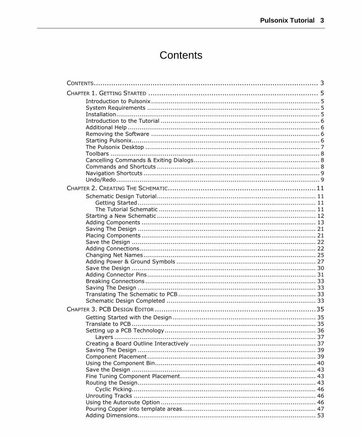
Contents
CONTENTS....................................................................................................... 3
CHAPTER 1. GETTING STARTED .............................................................................. 5 Introduction to Pulsonix ....................................................................................... 5 System Requirements ......................................................................................... 5 Installation ......................................................................................................... 5 Introduction to the Tutorial .................................................................................. 6 Additional Help ................................................................................................... 6 Removing the Software ....................................................................................... 6 Starting Pulsonix ................................................................................................. 6 The Pulsonix Desktop .......................................................................................... 7 Toolbars ............................................................................................................ 8 Cancelling Commands & Exiting Dialogs ................................................................. 8 Commands and Shortcuts .................................................................................... 8 Navigation Shortcuts ........................................................................................... 9 Undo/Redo ......................................................................................................... 9
CHAPTER 2. CREATING THE SCHEMATIC .................................................................... 11 Schematic Design Tutorial .................................................................................. 11
Getting Started ............................................................................................ 11 The Tutorial Schematic ................................................................................. 11
Starting a New Schematic .................................................................................. 12 Adding Components .......................................................................................... 13 Saving The Design ............................................................................................ 21 Placing Components .......................................................................................... 21 Save the Design ............................................................................................... 22 Adding Connections ........................................................................................... 22 Changing Net Names ......................................................................................... 25 Adding Power & Ground Symbols ........................................................................ 27 Save the Design ............................................................................................... 30 Adding Connector Pins ....................................................................................... 31 Breaking Connections ........................................................................................ 33 Saving The Design ............................................................................................ 33 Translating The Schematic to PCB ....................................................................... 33 Schematic Design Completed ............................................................................. 33
CHAPTER 3. PCB DESIGN EDITOR .......................................................................... 35 Getting Started with the Design .......................................................................... 35 Translate to PCB ............................................................................................... 35 Setting up a PCB Technology .............................................................................. 36
Layers ........................................................................................................ 37 Creating a Board Outline Interactively ................................................................. 37 Saving The Design ............................................................................................ 39 Component Placement ....................................................................................... 39 Using the Component Bin ................................................................................... 40 Save the Design ............................................................................................... 43 Fine Tuning Component Placement ...................................................................... 43 Routing the Design ............................................................................................ 43
Cyclic Picking ............................................................................................... 46 Unrouting Tracks .............................................................................................. 46 Using the Autoroute Option ................................................................................ 46 Pouring Copper into template areas ..................................................................... 47 Adding Dimensions............................................................................................ 53

4 Pulsonix Tutorial
Verifying Design Integrity .................................................................................. 54 Design Rules Checking....................................................................................... 55 Reports, Part Lists and Net Lists ......................................................................... 57 Plotting the Design ............................................................................................ 59 Additional Information ....................................................................................... 62
Pulsonix Tutorial 5
Chapter 1. Getting Started
Introduction to Pulsonix
Welcome to the Pulsonix electronic design system. The system is built on an integrated design environment using the intelligent Mosaic architecture providing all the tools required to capture a schematic and simulate it using the SPICE based analogue/digital simulator, through to the design and layout of the printed circuit board (PCB). This is aided with a powerful shape-based auto router.
Although Pulsonix is a sophisticated design tool it has also been created to be easy to use. It has been built around the Microsoft Windows style graphical user interface to provide a familiar operating environment. Although many of the CAD commands and menus are different from office and desktop programs, Pulsonix uses common commands where possible.
System Requirements
Pulsonix runs under the Windows operating systems but it is recommended that Windows 10 is used. It cannot run under MAC OS or Linux. Pulsonix does not require ‘high-powered’ hardware to achieve good performance, a regular off-the-shelf PC will be fine. A Pentium processor such as an i5 is sufficient.
Installation
To go through this tutorial, it is assumed that you have successfully installed the Pulsonix product onto your computer. If you haven’t, then install it using the download from the Pulsonix.com web site. The installation is straight forward using the wizard provided. Follow the instructions and use the default settings provided. Install Pulsonix in Demo mode (one of the options when installing). If you have an evaluation license supplied, this can also be used, a set of instructions would have been provided when you requested this type of license.
6 Pulsonix Tutorial
Introduction to the Tutorial
You can quickly familiarise yourself with the Pulsonix features available and its design methodology by working through this tutorial. The Online Help and Users Guide can be referenced for more detail as well.
This tutorial is broken down into logical sections following a Schematic and PCB design cycle.
The Schematic design editor is used to capture your logical design and ‘drive’ the PCB design. However, the PCB design editor can be used with or without the schematic design as you wish.
An important aspect of the PCB design is the production of professional manufacturing data, and hence the final PCB. Pulsonix has outputs to Gerber RS-274-D and RS-274-X, Excellon NC Drill outputs, pen plot outputs, Windows printer support, PDF output, ODB++, IPC-2581, IPC-D-356, Bill of materials, netlists, STEP, DXF, IDF and GenCAD format. Assembly machine outputs for pick & place machines etc., and JTN format files for the JTAG boundary scan products can also be output.
Additional Help
Help is available in a number of formats; Online help available by pressing <F1> at any time when using Pulsonix; by emailing us at [email protected], or by calling us or your local distributor. You will also find the Pulsonix Users Guide installed as a PDF file, this is instantly available from the Pulsonix Help menu and Online Manuals>
Removing the Software
If for any reason you wish to remove Pulsonix from your computer, re-run the Pulsonix installation program again and select Remove from the options presented.
Starting Pulsonix
During installation, a Pulsonix program icon is automatically added to your desktop and a Pulsonix program group added to the Start menu and Programs.
To start Pulsonix, simply double-click on the Pulsonix icon.
Pulsonix Tutorial 7
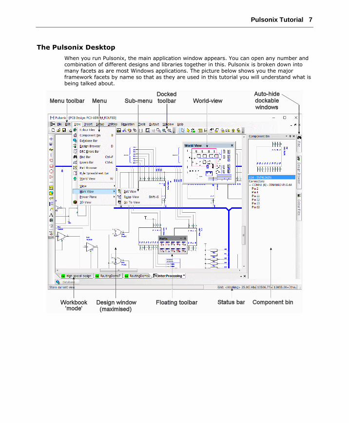
The Pulsonix Desktop
When you run Pulsonix, the main application window appears. You can open any number and combination of different designs and libraries together in this. Pulsonix is broken down into many facets as are most Windows applications. The picture below shows you the major framework facets by name so that as they are used in this tutorial you will understand what is being talked about.
8 Pulsonix Tutorial
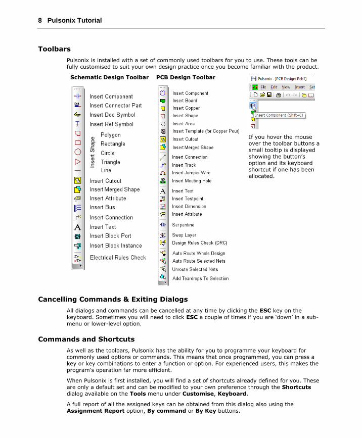
Toolbars
Pulsonix is installed with a set of commonly used toolbars for you to use. These tools can be fully customised to suit your own design practice once you become familiar with the product.
Schematic Design Toolbar
PCB Design Toolbar
If you hover the mouse over the toolbar buttons a small tooltip is displayed showing the button’s option and its keyboard shortcut if one has been allocated.
Cancelling Commands & Exiting Dialogs
All dialogs and commands can be cancelled at any time by clicking the ESC key on the
keyboard. Sometimes you will need to click ESC a couple of times if you are ‘down’ in a sub-menu or lower-level option.
Commands and Shortcuts
As well as the toolbars, Pulsonix has the ability for you to programme your keyboard for commonly used options or commands. This means that once programmed, you can press a key or key combinations to enter a function or option. For experienced users, this makes the program's operation far more efficient.
When Pulsonix is first installed, you will find a set of shortcuts already defined for you. These are only a default set and can be modified to your own preference through the Shortcuts dialog available on the Tools menu under Customise, Keyboard.
A full report of all the assigned keys can be obtained from this dialog also using the Assignment Report option, By command or By Key buttons.
Pulsonix Tutorial 9
Navigation Shortcuts
At this point, it is useful to mention some basic shortcuts used in Pulsonix to navigate a design:
• Zoom In - <Z> on the keyboard or roll the mouse wheel forward
• Zoom Out – <U> on the keyboard or roll the mouse wheel backwards
• Pan across the design – <P> on the keyboard or press and hold the mouse wheel
• View the whole design – <A> on the keyboard
Here are a couple of extra commands that will help you navigate Pulsonix, we will discuss these as they get used in the tutorial:
• Frame View – <F> on the keyboard. Zooms into a framed area of the design
• Layers Bar - Ctrl+L This is used to display and switch on/off Layers in the design
• Design Browser - <D> on the keyboard. A quick method of viewing and navigating your designs, especially useful when viewing hierarchical designs.
• Mirror/Flip – <M> on the keyboard. Flips a Schematic symbol in the X direction or flips a PCB component from one side of the board to another.
• Rotate – <R> on the keyboard. Rotates the Schematic symbol or PCB footprint by 90 degrees anti-clockwise (counter-clockwise).
Undo/Redo
Pulsonix contains unlimited multi-level Undo and Redo capabilities for use through the product. Undo and Redo are invoked using the standard Windows shortcut keys:
• Undo - Ctrl+Z
• Redo - Ctrl+Y

10 Pulsonix Tutorial
Pulsonix Tutorial 11
Chapter 2. Creating The Schematic
Schematic Design Tutorial
Getting Started
The following will show you how to create a small schematic design. Once you have completed it you can expand your knowledge to more complex functions within the schematic capture editor.
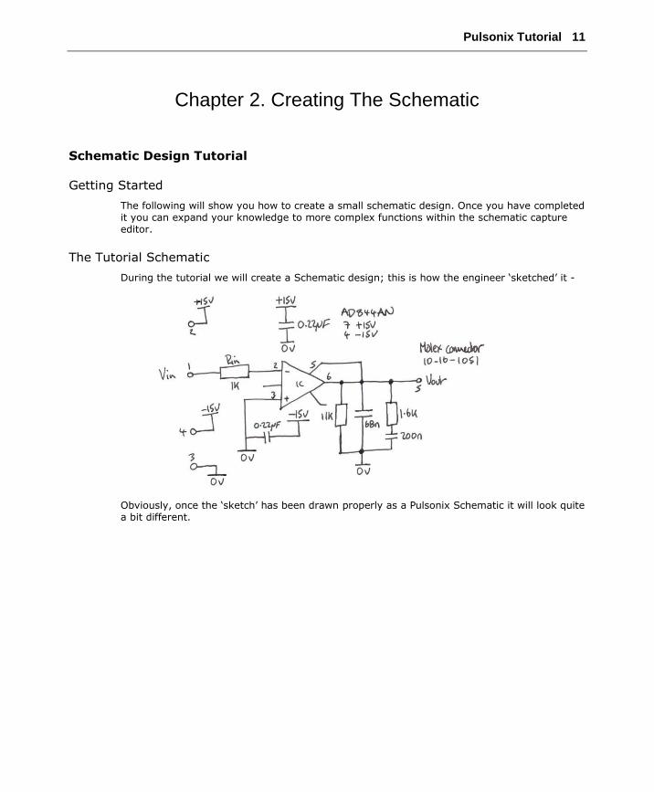
The Tutorial Schematic
During the tutorial we will create a Schematic design; this is how the engineer ‘sketched’ it -
Obviously, once the ‘sketch’ has been drawn properly as a Pulsonix Schematic it will look quite a bit different.
12 Pulsonix Tutorial
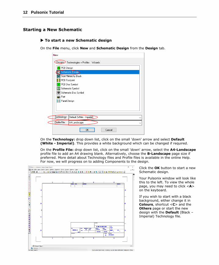
Starting a New Schematic
To start a new Schematic design
On the File menu, click New and Schematic Design from the Design tab.
On the Technology: drop down list, click on the small 'down' arrow and select Default (White - Imperial). This provides a white background which can be changed if required.
On the Profile File: drop down list, click on the small 'down' arrow, select the A4-Landscape profile file to add an A4 drawing blank. Alternatively, choose the B-Landscape page size if preferred. More detail about Technology files and Profile files is available in the online Help. For now, we will progress on to adding Components to the design.
Click the OK button to start a new Schematic design.
Your Pulsonix window will look like this to the left. To view the whole page, you may need to click <A> on the keyboard.
If you wish to start with a black background, either change it in Colours, shortcut <C> and the Others page or start the new design with the Default (Black – Imperial) Technology file.
Pulsonix Tutorial 13
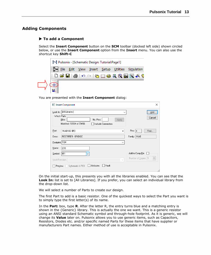
Adding Components
To add a Component
Select the Insert Component button on the SCM toolbar (docked left side) shown circled below, or use the Insert Component option from the Insert menu. You can also use the shortcut key Shift-C
You are presented with the Insert Component dialog:
On the initial start-up, this presents you with all the libraries enabled. You can see that the Look In: list is set to [All Libraries]. If you prefer, you can select an individual library from the drop-down list.
We will select a number of Parts to create our design.
The first Part to add is a basic resistor. One of the quickest ways to select the Part you want is to simply type the first letter(s) of its name.
In the Part: box, type R. After the letter R, the entry turns blue and a matching entry is shown in the {Generic} library. This is actually the one we want. This is a generic resistor using an ANSI standard Schematic symbol and through-hole footprint. As it is generic, we will change its Value later on. Pulsonix allows you to use generic items, such as Capacitors, Resistors, Diodes etc. and/or specific named Parts for these items that have supplier or manufacturers Part names. Either method of use is acceptable in Pulsonix.
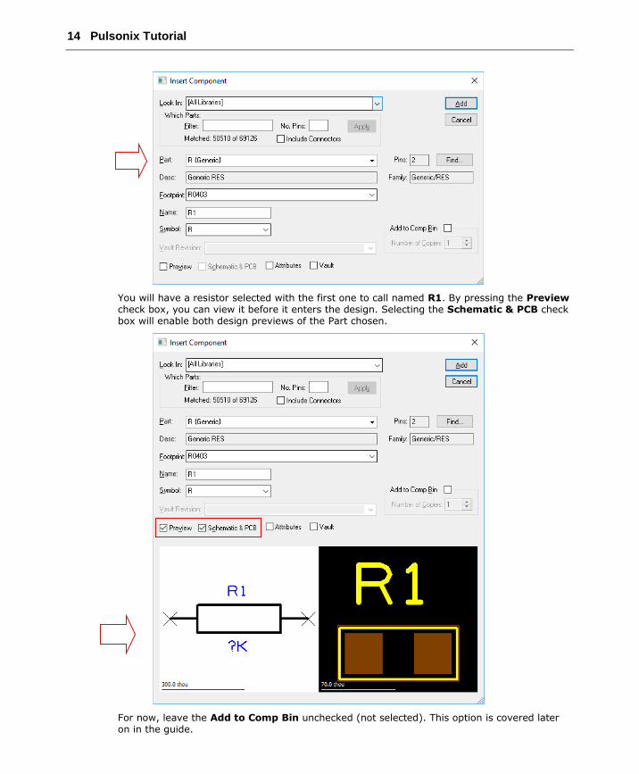
14 Pulsonix Tutorial
You will have a resistor selected with the first one to call named R1. By pressing the Preview check box, you can view it before it enters the design. Selecting the Schematic & PCB check box will enable both design previews of the Part chosen.
For now, leave the Add to Comp Bin unchecked (not selected). This option is covered later on in the guide.
Pulsonix Tutorial 15
Once you have the correct Part, you can add it to the design using the Add button.
The Add button will close the dialog from view and will allow you to interactively add as many Parts of the type selected to the design.
A small note here about Parts – a Part defined in the library is called a Component once added to the design.
The Component is currently on the end of your cursor. To place it in the design use a single mouse click. Place it somewhere to the centre left inside your drawing sheet. We will move it later on. If you wish to exit the dialog now, either press the <ESC> key or use the Cancel command in the context menu selected by pressing the right mouse button.
During this tutorial we will require 3 resistors in total. However, we will demonstrate different methods for adding components as they are required.
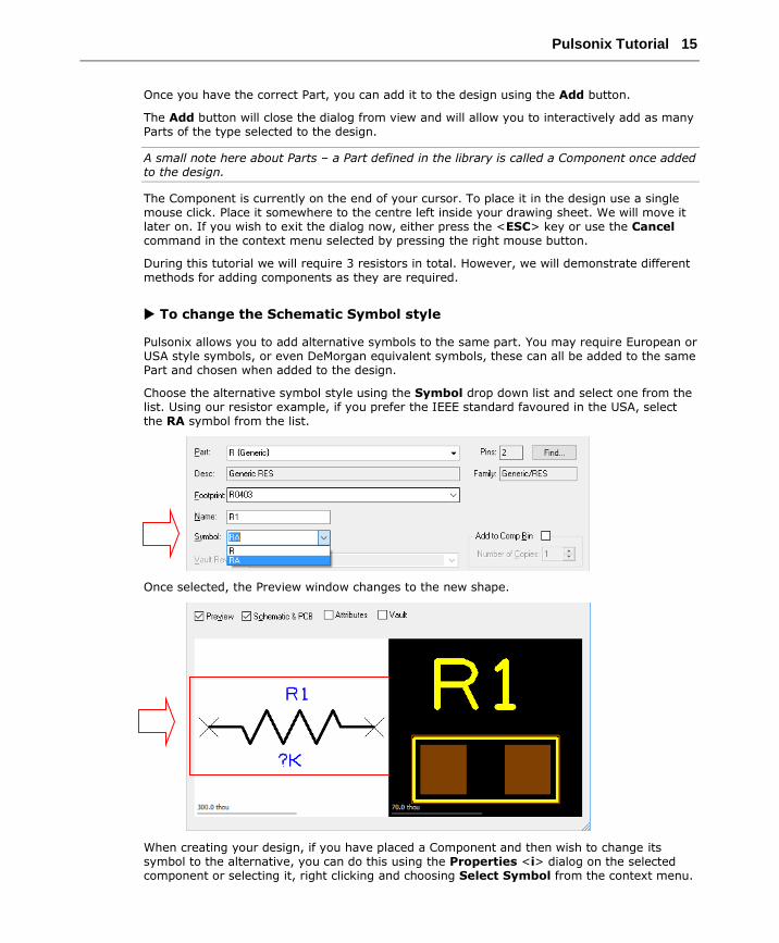
To change the Schematic Symbol style
Pulsonix allows you to add alternative symbols to the same part. You may require European or USA style symbols, or even DeMorgan equivalent symbols, these can all be added to the same Part and chosen when added to the design.
Choose the alternative symbol style using the Symbol drop down list and select one from the list. Using our resistor example, if you prefer the IEEE standard favoured in the USA, select the RA symbol from the list.
Once selected, the Preview window changes to the new shape.
When creating your design, if you have placed a Component and then wish to change its symbol to the alternative, you can do this using the Properties <i> dialog on the selected component or selecting it, right clicking and choosing Select Symbol from the context menu.
16 Pulsonix Tutorial
To pan & zoom in the design
To view more detail of the resistor in the design, roll the mouse wheel button forward to zoom in. If you zoom in too fast (and too far), roll the mouse wheel button backwards (slowly). If you zoom too far either way, press <A> on the keyboard to View All and then zoom in again.
If you prefer, use shortcut keys <Z> to zoom in and <U> to Zoom out.
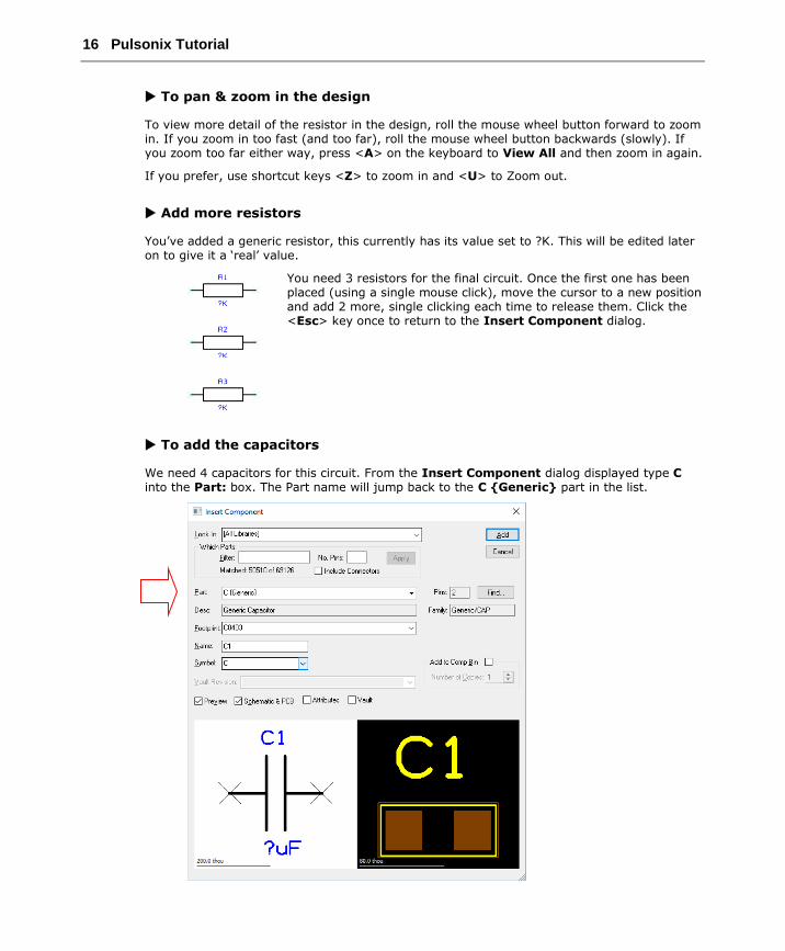
Add more resistors
You’ve added a generic resistor, this currently has its value set to ?K. This will be edited later on to give it a ‘real’ value.
You need 3 resistors for the final circuit. Once the first one has been placed (using a single mouse click), move the cursor to a new position and add 2 more, single clicking each time to release them. Click the <Esc> key once to return to the Insert Component dialog.
To add the capacitors
We need 4 capacitors for this circuit. From the Insert Component dialog displayed type C into the Part: box. The Part name will jump back to the C {Generic} part in the list.
Pulsonix Tutorial 17
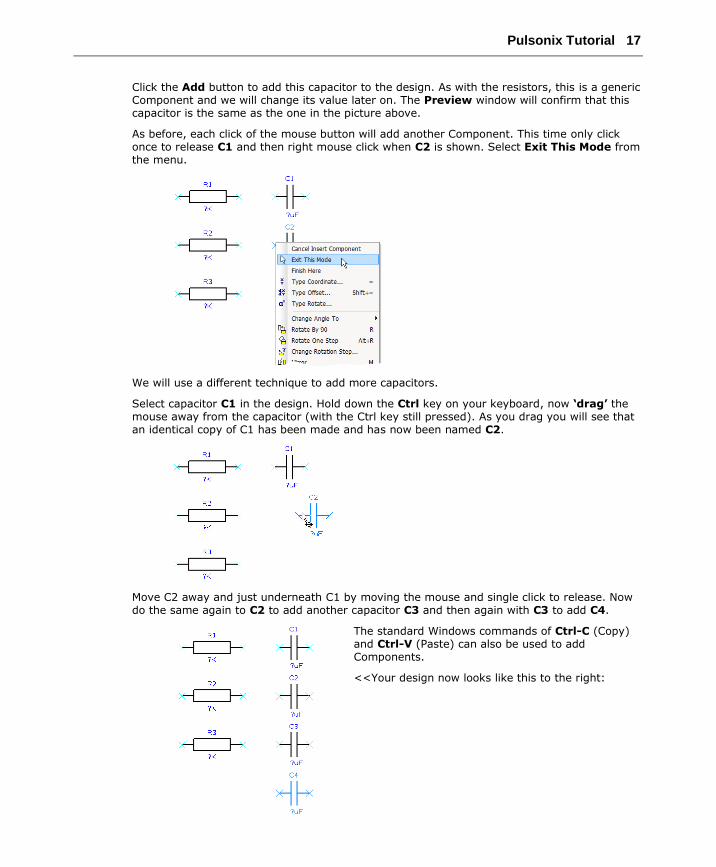
Click the Add button to add this capacitor to the design. As with the resistors, this is a generic Component and we will change its value later on. The Preview window will confirm that this capacitor is the same as the one in the picture above.
As before, each click of the mouse button will add another Component. This time only click once to release C1 and then right mouse click when C2 is shown. Select Exit This Mode from the menu.
We will use a different technique to add more capacitors.
Select capacitor C1 in the design. Hold down the Ctrl key on your keyboard, now ‘drag’ the mouse away from the capacitor (with the Ctrl key still pressed). As you drag you will see that an identical copy of C1 has been made and has now been named C2.
Move C2 away and just underneath C1 by moving the mouse and single click to release. Now do the same again to C2 to add another capacitor C3 and then again with C3 to add C4.
The standard Windows commands of Ctrl-C (Copy) and Ctrl-V (Paste) can also be used to add Components.
<<Your design now looks like this to the right:
18 Pulsonix Tutorial
To display a grid
Placement of components at this stage has been using a hidden grid that can be made visible. If you wish to see the grid in the design, switch it on using the shortcut key Ctrl-G. This command toggles the grid on and off.
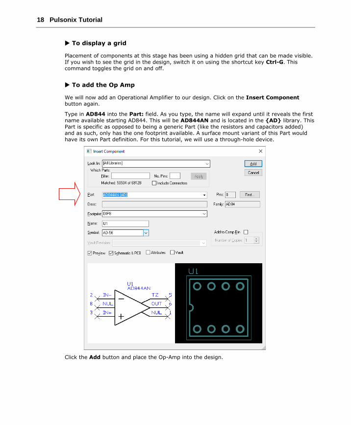
To add the Op Amp
We will now add an Operational Amplifier to our design. Click on the Insert Component button again.
Type in AD844 into the Part: field. As you type, the name will expand until it reveals the first name available starting AD844. This will be AD844AN and is located in the {AD} library. This Part is specific as opposed to being a generic Part (like the resistors and capacitors added) and as such, only has the one footprint available. A surface mount variant of this Part would have its own Part definition. For this tutorial, we will use a through-hole device.
Click the Add button and place the Op-Amp into the design.
Pulsonix Tutorial 19
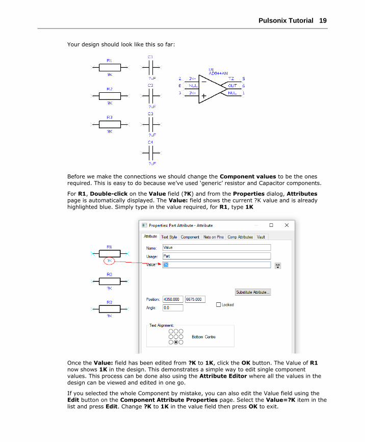
Your design should look like this so far:
Before we make the connections we should change the Component values to be the ones required. This is easy to do because we’ve used ‘generic’ resistor and Capacitor components.
For R1, Double-click on the Value field (?K) and from the Properties dialog, Attributes page is automatically displayed. The Value: field shows the current ?K value and is already highlighted blue. Simply type in the value required, for R1, type 1K
Once the Value: field has been edited from ?K to 1K, click the OK button. The Value of R1 now shows 1K in the design. This demonstrates a simple way to edit single component values. This process can be done also using the Attribute Editor where all the values in the design can be viewed and edited in one go.
If you selected the whole Component by mistake, you can also edit the Value field using the Edit button on the Component Attribute Properties page. Select the Value=?K item in the list and press Edit. Change ?K to 1K in the value field then press OK to exit.
20 Pulsonix Tutorial
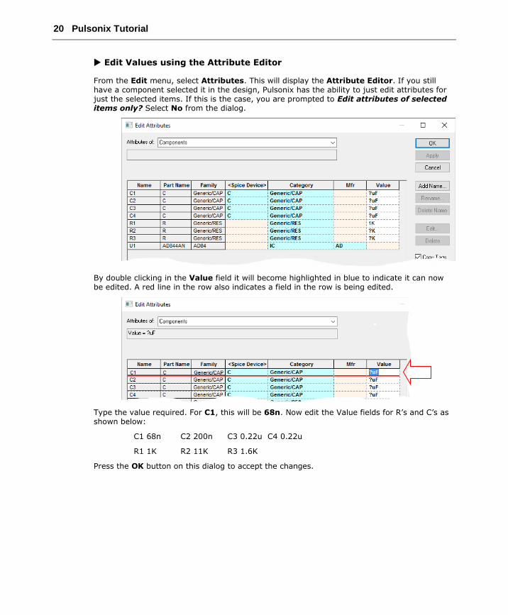
Edit Values using the Attribute Editor
From the Edit menu, select Attributes. This will display the Attribute Editor. If you still have a component selected it in the design, Pulsonix has the ability to just edit attributes for just the selected items. If this is the case, you are prompted to Edit attributes of selected items only? Select No from the dialog.
By double clicking in the Value field it will become highlighted in blue to indicate it can now be edited. A red line in the row also indicates a field in the row is being edited.
Type the value required. For C1, this will be 68n. Now edit the Value fields for R’s and C’s as shown below:
C1 68n C2 200n C3 0.22u C4 0.22u
R1 1K R2 11K R3 1.6K
Press the OK button on this dialog to accept the changes.
Pulsonix Tutorial 21
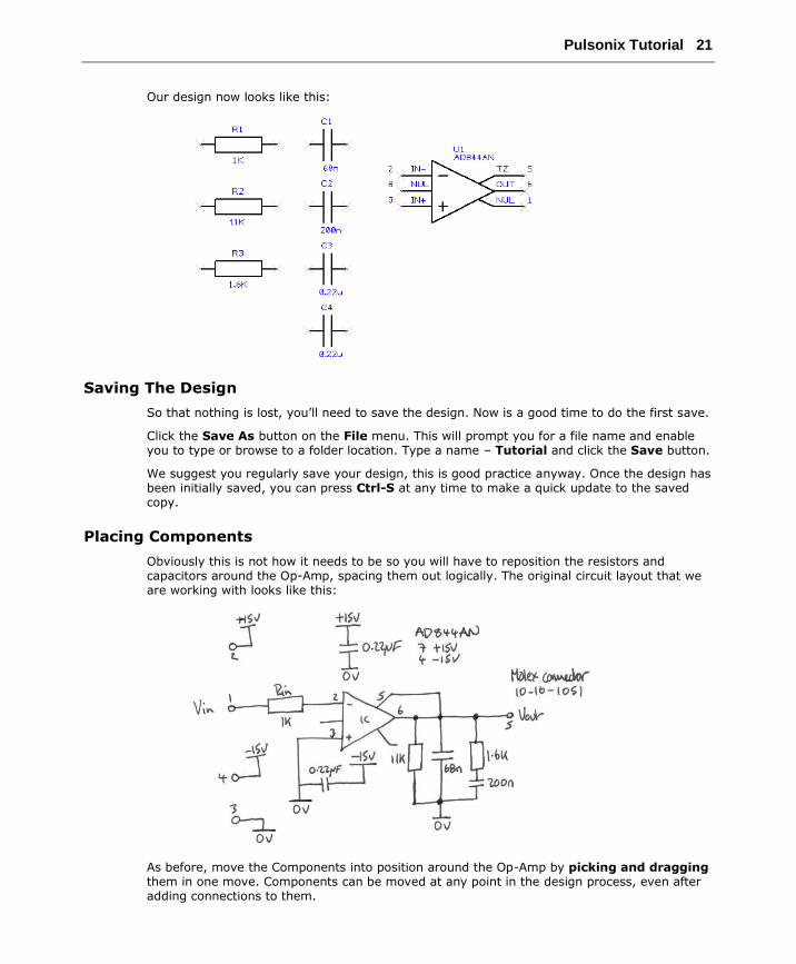
Our design now looks like this:
Saving The Design
So that nothing is lost, you’ll need to save the design. Now is a good time to do the first save.
Click the Save As button on the File menu. This will prompt you for a file name and enable you to type or browse to a folder location. Type a name – Tutorial and click the Save button.
We suggest you regularly save your design, this is good practice anyway. Once the design has been initially saved, you can press Ctrl-S at any time to make a quick update to the saved copy.
Placing Components
Obviously this is not how it needs to be so you will have to reposition the resistors and capacitors around the Op-Amp, spacing them out logically. The original circuit layout that we are working with looks like this:
As before, move the Components into position around the Op-Amp by picking and dragging them in one move. Components can be moved at any point in the design process, even after adding connections to them.
22 Pulsonix Tutorial
Rotating Components
Components that need to be rotated during move can be by clicking the shortcut key <R>. A single click of the <R> key will rotate the component by 90 degrees. Click <R> more than once to rotate it in 90 degrees steps.
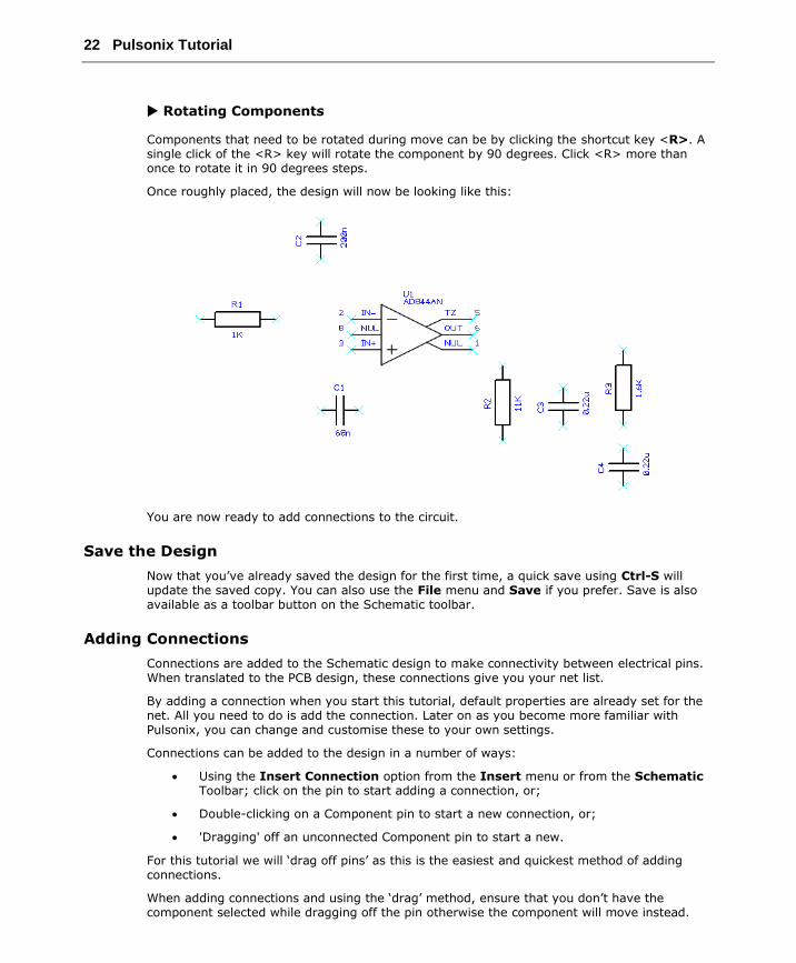
Once roughly placed, the design will now be looking like this:
You are now ready to add connections to the circuit.
Save the Design
Now that you’ve already saved the design for the first time, a quick save using Ctrl-S will update the saved copy. You can also use the File menu and Save if you prefer. Save is also available as a toolbar button on the Schematic toolbar.
Adding Connections
Connections are added to the Schematic design to make connectivity between electrical pins. When translated to the PCB design, these connections give you your net list.
By adding a connection when you start this tutorial, default properties are already set for the net. All you need to do is add the connection. Later on as you become more familiar with Pulsonix, you can change and customise these to your own settings.
Connections can be added to the design in a number of ways:
• Using the Insert Connection option from the Insert menu or from the Schematic Toolbar; click on the pin to start adding a connection, or;
• Double-clicking on a Component pin to start a new connection, or;
• 'Dragging' off an unconnected Component pin to start a new.
For this tutorial we will ‘drag off pins’ as this is the easiest and quickest method of adding connections.
When adding connections and using the ‘drag’ method, ensure that you don’t have the component selected while dragging off the pin otherwise the component will move instead.
Pulsonix Tutorial 23
To add connections by dragging off pins
When ‘dragging’ off an electrical pin to start a new connection, once started, you simply move the cursor around. You do not need to hold the mouse key down. In the default mode, from start, there are always two dynamic orthogonal connection lines displayed. Moving the cursor up and down, left and right extends the connection vertices.
If you wish to force a corner, left click the mouse, you can also press the <Space bar> if you prefer. This will then start you in the next two axis orthogonal connection path.
Moving close to or over another electrical pin will show a modal cursor; a slightly different cursor from the standard Windows one with an indication of its status. When over a legal electrical pin, an ‘F’ on the cursor is displayed, F for Finish, indicating you can finish here. A single click of the left mouse button will finish the connection there.
At any point during the addition of the connection, you wish to go back, you can either ‘reroute’ on itself, in which case the Remove Loops cursor is displayed and the extra section of connection remove once a corner is added:
Or, you can use the <Backspace> key on the keyboard to remove the last connection segment.
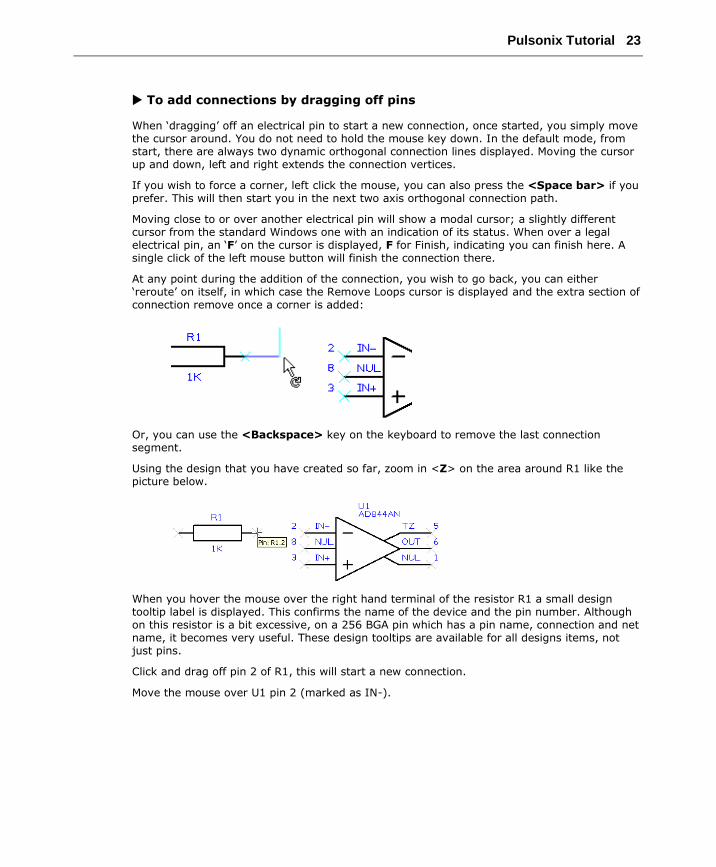
Using the design that you have created so far, zoom in <Z> on the area around R1 like the picture below.
When you hover the mouse over the right hand terminal of the resistor R1 a small design tooltip label is displayed. This confirms the name of the device and the pin number. Although on this resistor is a bit excessive, on a 256 BGA pin which has a pin name, connection and net name, it becomes very useful. These design tooltips are available for all designs items, not just pins.
Click and drag off pin 2 of R1, this will start a new connection.
Move the mouse over U1 pin 2 (marked as IN-).
24 Pulsonix Tutorial
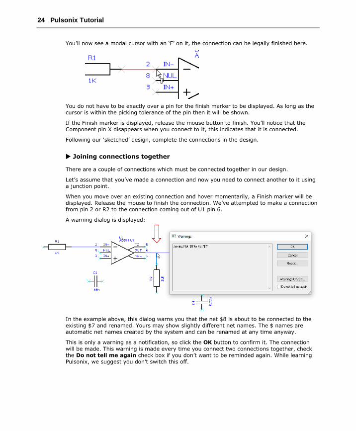
You’ll now see a modal cursor with an ‘F’ on it, the connection can be legally finished here.
You do not have to be exactly over a pin for the finish marker to be displayed. As long as the cursor is within the picking tolerance of the pin then it will be shown.
If the Finish marker is displayed, release the mouse button to finish. You’ll notice that the Component pin X disappears when you connect to it, this indicates that it is connected.
Following our ‘sketched’ design, complete the connections in the design.
Joining connections together
There are a couple of connections which must be connected together in our design.
Let’s assume that you’ve made a connection and now you need to connect another to it using a junction point.
When you move over an existing connection and hover momentarily, a Finish marker will be displayed. Release the mouse to finish the connection. We’ve attempted to make a connection from pin 2 or R2 to the connection coming out of U1 pin 6.
A warning dialog is displayed:
In the example above, this dialog warns you that the net $8 is about to be connected to the existing $7 and renamed. Yours may show slightly different net names. The $ names are automatic net names created by the system and can be renamed at any time anyway.
This is only a warning as a notification, so click the OK button to confirm it. The connection
will be made. This warning is made every time you connect two connections together, check the Do not tell me again check box if you don’t want to be reminded again. While learning Pulsonix, we suggest you don’t switch this off.
Pulsonix Tutorial 25
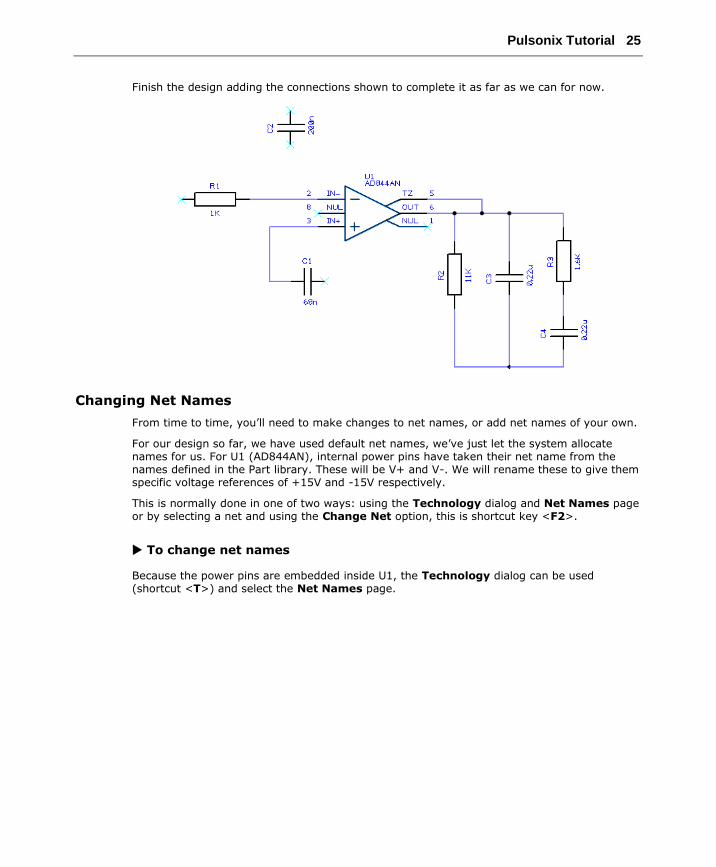
Finish the design adding the connections shown to complete it as far as we can for now.
Changing Net Names
From time to time, you’ll need to make changes to net names, or add net names of your own.
For our design so far, we have used default net names, we’ve just let the system allocate names for us. For U1 (AD844AN), internal power pins have taken their net name from the names defined in the Part library. These will be V+ and V-. We will rename these to give them specific voltage references of +15V and -15V respectively.
This is normally done in one of two ways: using the Technology dialog and Net Names page or by selecting a net and using the Change Net option, this is shortcut key <F2>.
To change net names
Because the power pins are embedded inside U1, the Technology dialog can be used (shortcut <T>) and select the Net Names page.
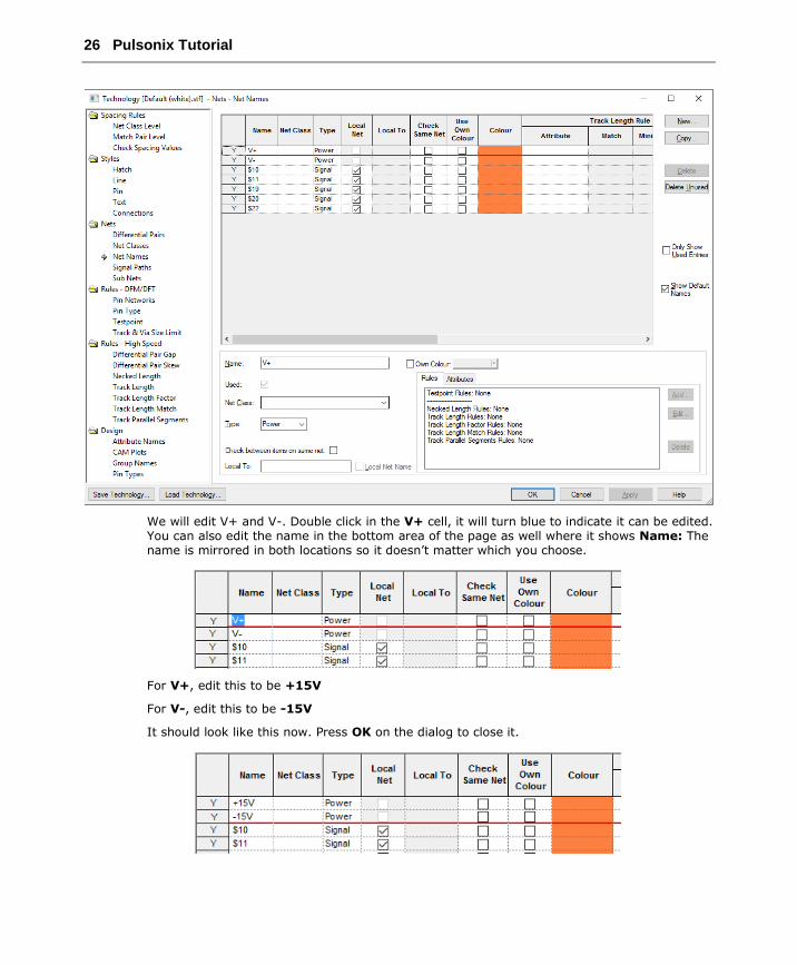
26 Pulsonix Tutorial
We will edit V+ and V-. Double click in the V+ cell, it will turn blue to indicate it can be edited. You can also edit the name in the bottom area of the page as well where it shows Name: The name is mirrored in both locations so it doesn’t matter which you choose.
For V+, edit this to be +15V
For V-, edit this to be -15V
It should look like this now. Press OK on the dialog to close it.
Pulsonix Tutorial 27
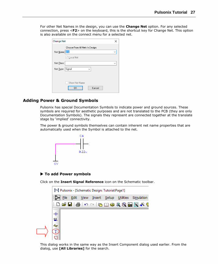
For other Net Names in the design, you can use the Change Net option. For any selected connection, press <F2> on the keyboard, this is the shortcut key for Change Net. This option is also available on the connect menu for a selected net.
Adding Power & Ground Symbols
Pulsonix has special Documentation Symbols to indicate power and ground sources. These symbols are required for aesthetic purposes and are not translated to the PCB (they are only Documentation Symbols). The signals they represent are connected together at the translate stage by ‘implied’ connectivity.
The power & ground symbols themselves can contain inherent net name properties that are automatically used when the Symbol is attached to the net.
To add Power symbols
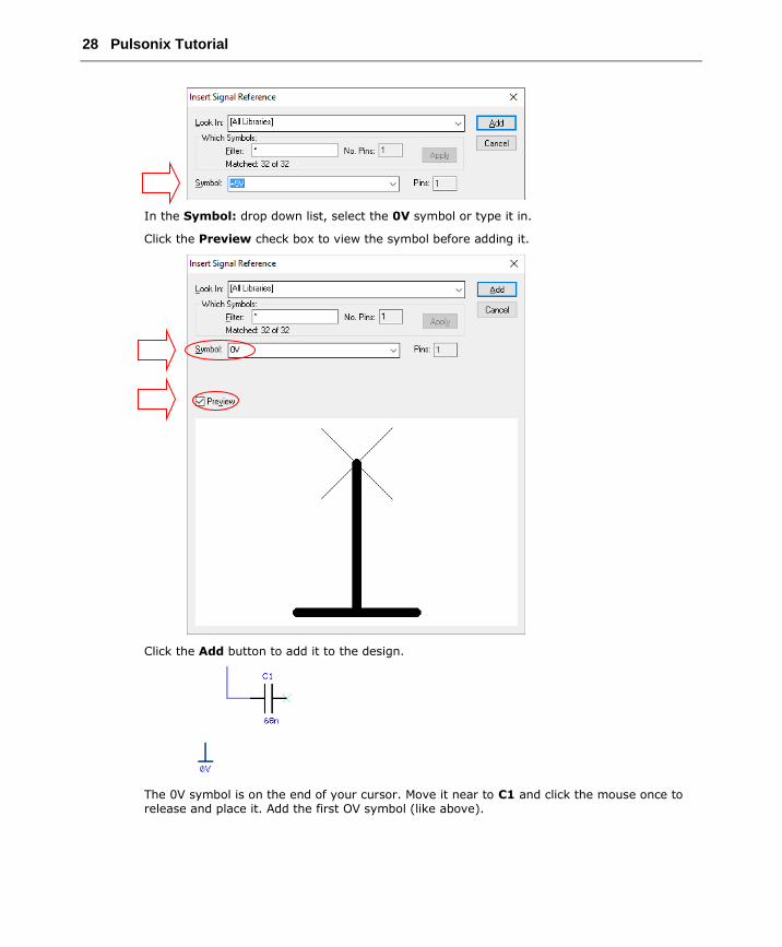
Click on the Insert Signal Reference icon on the Schematic toolbar.
This dialog works in the same way as the Insert Component dialog used earlier. From the dialog, use [All Libraries] for the search.
28 Pulsonix Tutorial
In the Symbol: drop down list, select the 0V symbol or type it in.
Click the Preview check box to view the symbol before adding it.
Click the Add button to add it to the design.
The 0V symbol is on the end of your cursor. Move it near to C1 and click the mouse once to release and place it. Add the first OV symbol (like above).
Pulsonix Tutorial 29
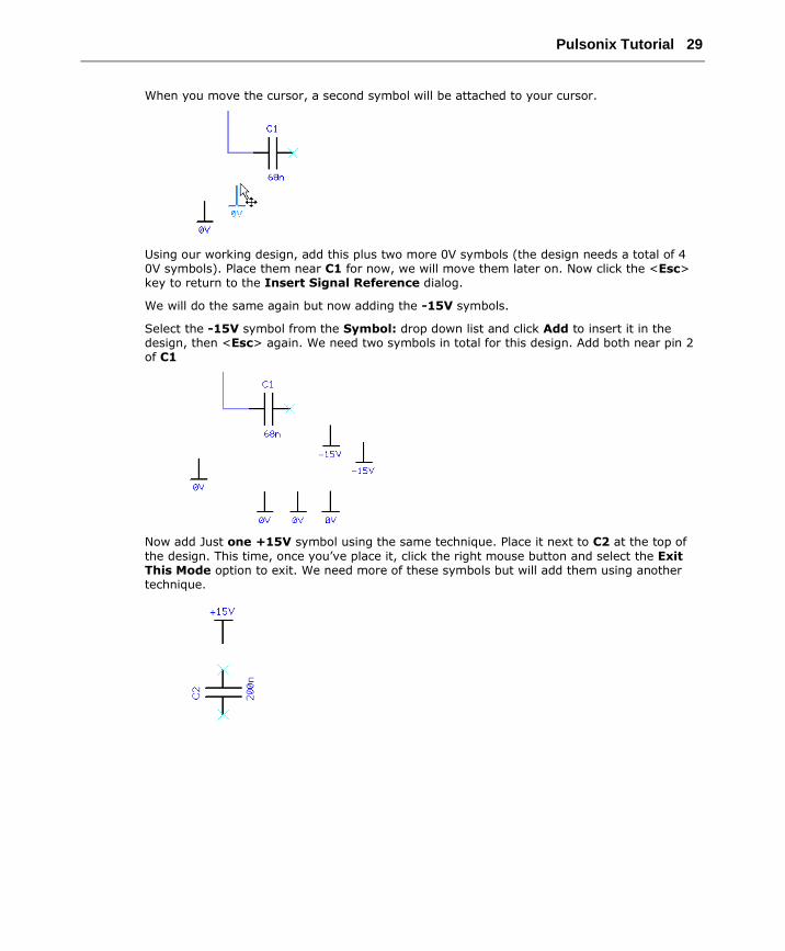
When you move the cursor, a second symbol will be attached to your cursor.
Using our working design, add this plus two more 0V symbols (the design needs a total of 4 0V symbols). Place them near C1 for now, we will move them later on. Now click the <Esc> key to return to the Insert Signal Reference dialog.
We will do the same again but now adding the -15V symbols.
Select the -15V symbol from the Symbol: drop down list and click Add to insert it in the design, then <Esc> again. We need two symbols in total for this design. Add both near pin 2 of C1
Now add Just one +15V symbol using the same technique. Place it next to C2 at the top of
the design. This time, once you’ve place it, click the right mouse button and select the Exit This Mode option to exit. We need more of these symbols but will add them using another technique.
30 Pulsonix Tutorial
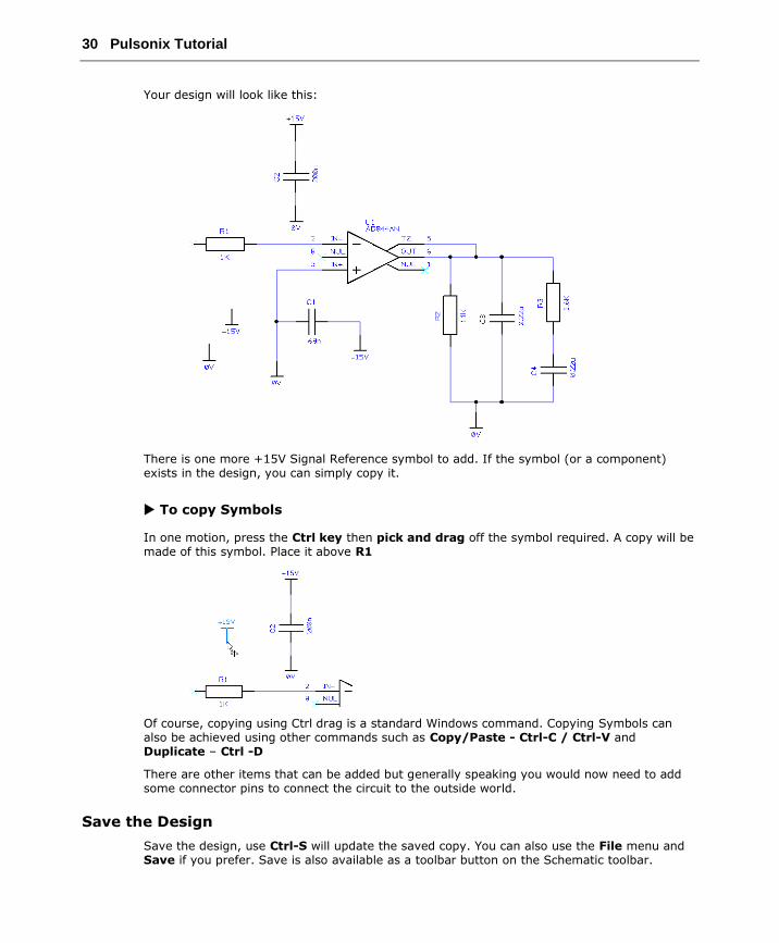
Your design will look like this:
There is one more +15V Signal Reference symbol to add. If the symbol (or a component) exists in the design, you can simply copy it.
To copy Symbols
In one motion, press the Ctrl key then pick and drag off the symbol required. A copy will be made of this symbol. Place it above R1
Of course, copying using Ctrl drag is a standard Windows command. Copying Symbols can also be achieved using other commands such as Copy/Paste - Ctrl-C / Ctrl-V and Duplicate – Ctrl -D
There are other items that can be added but generally speaking you would now need to add some connector pins to connect the circuit to the outside world.
Save the Design
Save the design, use Ctrl-S will update the saved copy. You can also use the File menu and Save if you prefer. Save is also available as a toolbar button on the Schematic toolbar.
Pulsonix Tutorial 31
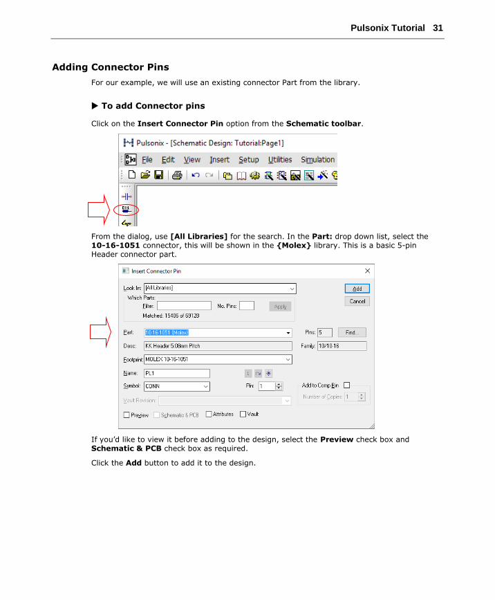
Adding Connector Pins
For our example, we will use an existing connector Part from the library.
To add Connector pins
Click on the Insert Connector Pin option from the Schematic toolbar.
From the dialog, use [All Libraries] for the search. In the Part: drop down list, select the 10-16-1051 connector, this will be shown in the {Molex} library. This is a basic 5-pin Header connector part.
If you’d like to view it before adding to the design, select the Preview check box and Schematic & PCB check box as required.
Click the Add button to add it to the design.
32 Pulsonix Tutorial
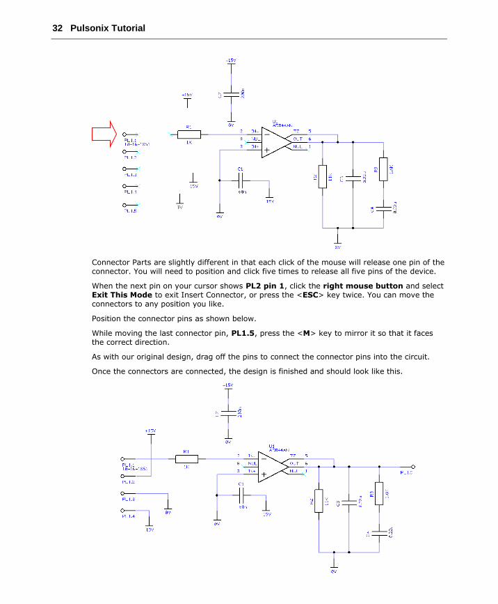
Connector Parts are slightly different in that each click of the mouse will release one pin of the connector. You will need to position and click five times to release all five pins of the device.
When the next pin on your cursor shows PL2 pin 1, click the right mouse button and select Exit This Mode to exit Insert Connector, or press the <ESC> key twice. You can move the connectors to any position you like.
Position the connector pins as shown below.
While moving the last connector pin, PL1.5, press the <M> key to mirror it so that it faces the correct direction.
As with our original design, drag off the pins to connect the connector pins into the circuit.
Once the connectors are connected, the design is finished and should look like this.
Pulsonix Tutorial 33
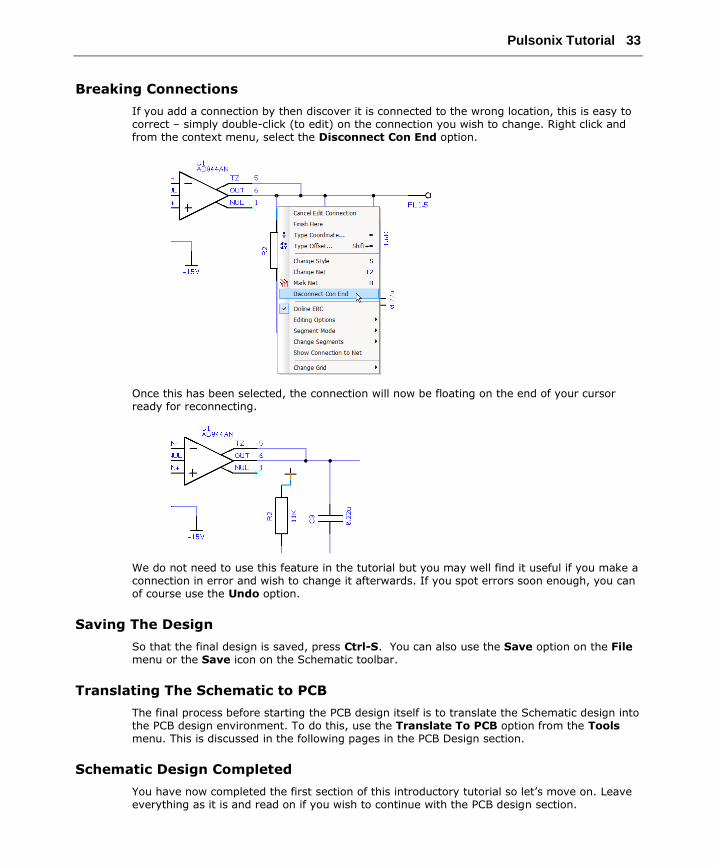
Breaking Connections
If you add a connection by then discover it is connected to the wrong location, this is easy to correct – simply double-click (to edit) on the connection you wish to change. Right click and from the context menu, select the Disconnect Con End option.
Once this has been selected, the connection will now be floating on the end of your cursor ready for reconnecting.
We do not need to use this feature in the tutorial but you may well find it useful if you make a connection in error and wish to change it afterwards. If you spot errors soon enough, you can of course use the Undo option.
Saving The Design
So that the final design is saved, press Ctrl-S. You can also use the Save option on the File menu or the Save icon on the Schematic toolbar.
Translating The Schematic to PCB
The final process before starting the PCB design itself is to translate the Schematic design into the PCB design environment. To do this, use the Translate To PCB option from the Tools menu. This is discussed in the following pages in the PCB Design section.
Schematic Design Completed
You have now completed the first section of this introductory tutorial so let’s move on. Leave everything as it is and read on if you wish to continue with the PCB design section.

34 Pulsonix Tutorial
Pulsonix Tutorial 35
Chapter 3. PCB Design Editor
Getting Started with the Design
Pulsonix PCB is flexible in that you can start your layout in a number of ways:
• Use Pulsonix Schematic Capture as the 'front-end' to the PCB system. The nets and Components are translated to PCB in the integrated environment.
• Use a netlist that is derived from another Schematic or CAE system.
• Use the Pulsonix PCB design editor interactively creating the design on-the-fly without the need for an initial netlist or Schematic. You can just add connections and Components straight into the PCB design editor to create design.
Translate to PCB
For our tutorial, we will take the ‘logical’ Schematic design created in the previous section and convert it to a ‘physical’ PCB layout.
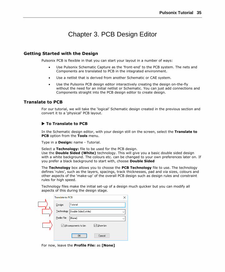
To Translate to PCB
In the Schematic design editor, with your design still on the screen, select the Translate to PCB option from the Tools menu.
Type in a Design: name - Tutorial.
Select a Technology: file to be used for the PCB design. Use the Double Sided (White) technology. This will give you a basic double sided design with a white background. The colours etc. can be changed to your own preferences later on. If
you prefer a black background to start with, choose Double Sided
The Technology box allows you to choose the PCB Technology file to use. The technology defines ‘rules’, such as the layers, spacings, track thicknesses, pad and via sizes, colours and other aspects of the ‘make-up’ of the overall PCB design such as design rules and constraint rules for high speed.
Technology files make the initial set-up of a design much quicker but you can modify all aspects of this during the design stage.
For now, leave the Profile File: as [None]
36 Pulsonix Tutorial
PCB Profile files allow you to define some physical aspects of the board, such as the board outline, critical Component placement and other general annotation such as the drawing borders, assembly and manufacturing text, drill tables etc.
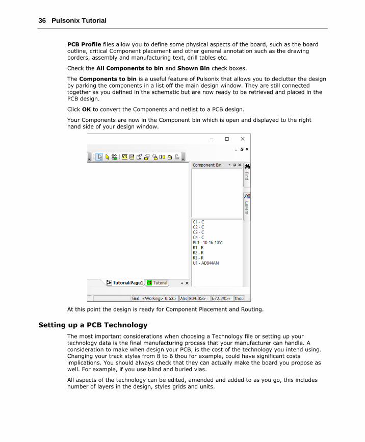
Check the All Components to bin and Shown Bin check boxes.
The Components to bin is a useful feature of Pulsonix that allows you to declutter the design by parking the components in a list off the main design window. They are still connected together as you defined in the schematic but are now ready to be retrieved and placed in the PCB design.
Click OK to convert the Components and netlist to a PCB design.
Your Components are now in the Component bin which is open and displayed to the right hand side of your design window.
At this point the design is ready for Component Placement and Routing.
Setting up a PCB Technology
The most important considerations when choosing a Technology file or setting up your technology data is the final manufacturing process that your manufacturer can handle. A consideration to make when design your PCB, is the cost of the technology you intend using. Changing your track styles from 8 to 6 thou for example, could have significant costs implications. You should always check that they can actually make the board you propose as well. For example, if you use blind and buried vias.
All aspects of the technology can be edited, amended and added to as you go, this includes number of layers in the design, styles grids and units.
Pulsonix Tutorial 37
For this exercise, we have chosen to use a pre-defined technology file, Double Sided (White) IMP, which as it name suggests, provides you with a two-layer PCB with a set of general purpose styles and sizes. The (White) in the name suggests that screen background is white, this can be easily changed if you prefer a black background or another colour. IMP indicates this technology file is defined in Imperial units of Thou (Mils).
Layers
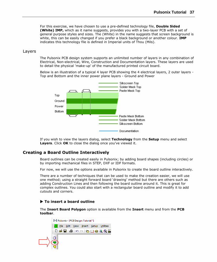
The Pulsonix PCB design system supports an unlimited number of layers in any combination of Electrical, Non-electrical, Wire, Construction and Documentation layers. These layers are used to detail the physical 'make-up' of the manufactured printed circuit board.
Below is an illustration of a typical 4 layer PCB showing the 4 electrical layers, 2 outer layers - Top and Bottom and the inner power plane layers - Ground and Power
If you wish to view the layers dialog, select Technology from the Setup menu and select Layers. Click OK to close the dialog once you’ve viewed it.
Creating a Board Outline Interactively
Board outlines can be created easily in Pulsonix; by adding board shapes (including circles) or by importing mechanical files in STEP, DXF or IDF formats.
For now, we will use the options available in Pulsonix to create the board outline interactively.
There are a number of techniques that can be used to make the creation easier, we will use one method; using a straight forward board ‘drawing’ method but there are others such as adding Construction Lines and then following the board outline around it. This is great for complex outlines. You could also start with a rectangular board outline and modify it to add cutouts and corners.
To insert a board outline
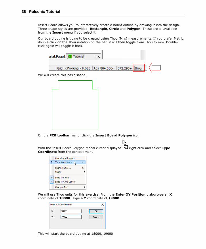
The Insert Board Polygon option is available from the Insert menu and from the PCB toolbar.
38 Pulsonix Tutorial
Insert Board allows you to interactively create a board outline by drawing it into the design. Three shape styles are provided: Rectangle, Circle and Polygon. These are all available from the Insert menu if you select it.
Our board outline is going to be created using Thou (Mils) measurements. If you prefer Metric, double-click on the Thou notation on the bar, it will then toggle from Thou to mm. Double-click again will toggle it back.
We will create this basic shape:
On the PCB toolbar menu, click the Insert Board Polygon icon.
With the Insert Board Polygon modal cursor displayed right click and select Type
Coordinate from the context menu.
We will use Thou units for this exercise. From the Enter XY Position dialog type an X coordinate of 18000. Type a Y coordinate of 19000
This will start the board outline at 18000, 19000
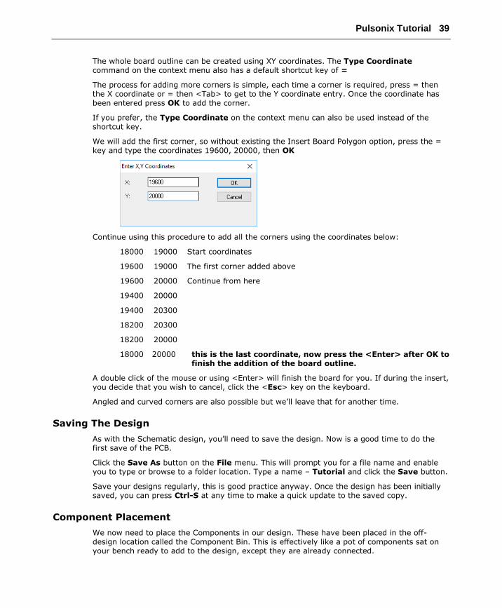
Pulsonix Tutorial 39
The whole board outline can be created using XY coordinates. The Type Coordinate command on the context menu also has a default shortcut key of =
The process for adding more corners is simple, each time a corner is required, press = then the X coordinate or = then <Tab> to get to the Y coordinate entry. Once the coordinate has been entered press OK to add the corner.
If you prefer, the Type Coordinate on the context menu can also be used instead of the shortcut key.
We will add the first corner, so without existing the Insert Board Polygon option, press the = key and type the coordinates 19600, 20000, then OK
Continue using this procedure to add all the corners using the coordinates below:
18000 19000 Start coordinates
19600 19000 The first corner added above
19600 20000 Continue from here
19400 20000
19400 20300
18200 20300
18200 20000
18000 20000 this is the last coordinate, now press the <Enter> after OK to finish the addition of the board outline.
A double click of the mouse or using <Enter> will finish the board for you. If during the insert, you decide that you wish to cancel, click the <Esc> key on the keyboard.
Angled and curved corners are also possible but we’ll leave that for another time.
Saving The Design
As with the Schematic design, you’ll need to save the design. Now is a good time to do the first save of the PCB.
Click the Save As button on the File menu. This will prompt you for a file name and enable you to type or browse to a folder location. Type a name – Tutorial and click the Save button.
Save your designs regularly, this is good practice anyway. Once the design has been initially saved, you can press Ctrl-S at any time to make a quick update to the saved copy.
Component Placement
We now need to place the Components in our design. These have been placed in the off-design location called the Component Bin. This is effectively like a pot of components sat on your bench ready to add to the design, except they are already connected.
40 Pulsonix Tutorial
Using the Component Bin
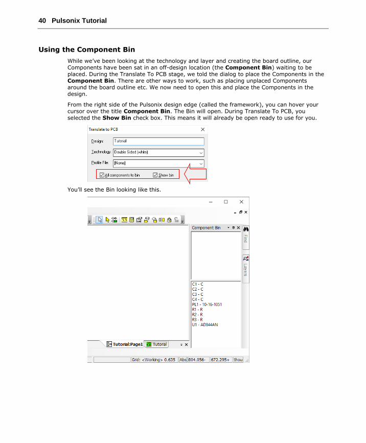
While we’ve been looking at the technology and layer and creating the board outline, our Components have been sat in an off-design location (the Component Bin) waiting to be placed. During the Translate To PCB stage, we told the dialog to place the Components in the Component Bin. There are other ways to work, such as placing unplaced Components around the board outline etc. We now need to open this and place the Components in the design.
From the right side of the Pulsonix design edge (called the framework), you can hover your cursor over the title Component Bin. The Bin will open. During Translate To PCB, you selected the Show Bin check box. This means it will already be open ready to use for you.
You’ll see the Bin looking like this.
Pulsonix Tutorial 41
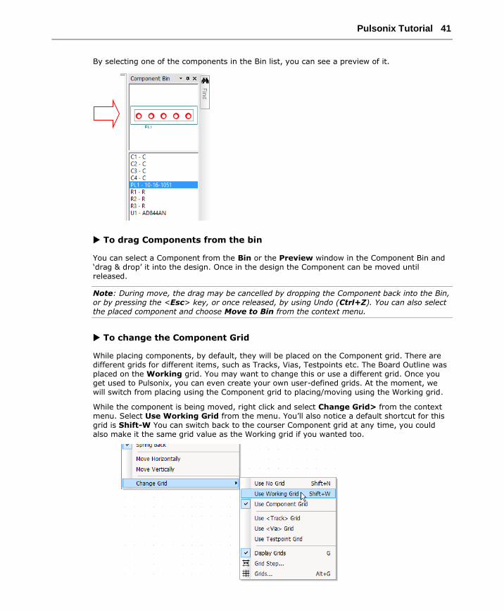
By selecting one of the components in the Bin list, you can see a preview of it.
To drag Components from the bin
You can select a Component from the Bin or the Preview window in the Component Bin and ‘drag & drop’ it into the design. Once in the design the Component can be moved until released.
Note: During move, the drag may be cancelled by dropping the Component back into the Bin, or by pressing the <Esc> key, or once released, by using Undo (Ctrl+Z). You can also select the placed component and choose Move to Bin from the context menu.
To change the Component Grid
While placing components, by default, they will be placed on the Component grid. There are different grids for different items, such as Tracks, Vias, Testpoints etc. The Board Outline was placed on the Working grid. You may want to change this or use a different grid. Once you get used to Pulsonix, you can even create your own user-defined grids. At the moment, we will switch from placing using the Component grid to placing/moving using the Working grid.
While the component is being moved, right click and select Change Grid> from the context menu. Select Use Working Grid from the menu. You’ll also notice a default shortcut for this grid is Shift-W You can switch back to the courser Component grid at any time, you could also make it the same grid value as the Working grid if you wanted too.

42 Pulsonix Tutorial
By default, the Component grid has been set fairly coarsely at 100 Thou and the Working grid set finer at 25 Thou. These can both be changed (as can all the system grids).
For now, switch to the Working Grid and place the connector PL1 into the ‘slot’ in the board.
Next, the logical step would be to place the IC, U1. Drag it out of the bin and place it somewhere in the centre of the design. Let’s change the colour of the connections so they are more visible.
To change the connection colour
From the Setup menu, select Colours. You can also use a shortcut key <C> or select the Colours icon from the Standard toolbar.
From the Others page, select the colour picker for Connections. Choose a colour of your liking and press OK to exit the dialog. Colours for all design items can be changed here too such as swapping to a black background. In fact, this can be done on this same page by selecting the colour for Background.
Finish placing the components
Place all the Components to look like the picture below. It is suggested you place PL1 and U1 first then place the other Components around these. Placement in this design is not critical, you can probably place it much more efficiently!
Pulsonix Tutorial 43
To minimise connection lengths
Once placed, if you wish, you can minimise the length of connections by using the Optimise Nets feature. From the Tools menu, select Optimise Nets> All Nets Shortcut key Shift+O
Save the Design
Now that you’ve already saved the design for the first time, a quick save using Ctrl-S will update the saved copy. You can also use the File menu and Save if you prefer. Save is also available as a toolbar button on the Schematic toolbar.
Fine Tuning Component Placement
Once the Components have been dragged from the bin you can place them in the design. Use shortcut keys <R> to rotate them and <M> to Mirror surface mount Components, these options (and more) are available on the shortcut menu during Move. For our design, no rotation or mirroring will be required. Once fully placed, the design should be routed.
Routing the Design
The design can be routed manually or automatically. This is the process of converting the electrical point-to-point connections into physical copper ‘tracks’.
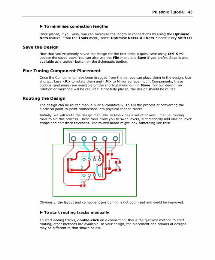
Initially, we will route the design manually. Pulsonix has a set of powerful manual routing tools to aid this process. These tools allow you to swap layers, automatically add vias on layer swaps and edit track thickness. The routed board might look something like this:
Obviously, the layout and component positioning is not optimised and could be improved.
To start routing tracks manually
To start adding tracks, double-click on a connection, this is the quickest method to start routing, other methods are available. In your design, the placement and colours of designs may be different to that shown below.
44 Pulsonix Tutorial
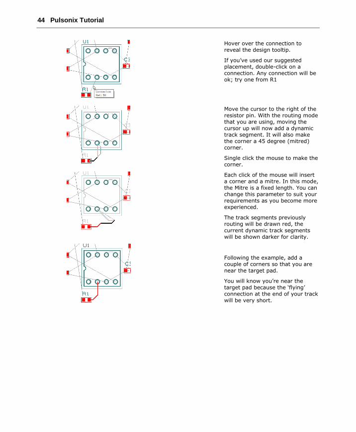
Hover over the connection to reveal the design tooltip.
If you’ve used our suggested placement, double-click on a connection. Any connection will be ok; try one from R1
Move the cursor to the right of the resistor pin. With the routing mode that you are using, moving the cursor up will now add a dynamic track segment. It will also make the corner a 45 degree (mitred) corner.
Single click the mouse to make the corner.
Each click of the mouse will insert a corner and a mitre. In this mode, the Mitre is a fixed length. You can change this parameter to suit your requirements as you become more experienced.
The track segments previously routing will be drawn red, the current dynamic track segments will be shown darker for clarity.
Following the example, add a couple of corners so that you are near the target pad.
You will know you’re near the target pad because the ‘flying’ connection at the end of your track will be very short.
Pulsonix Tutorial 45
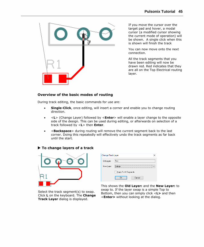
If you move the cursor over the target pad and hover, a modal cursor (a modified cursor showing the current mode of operation) will be shown. A single click when this is shown will finish the track
You can now move onto the next connection.
All the track segments that you have been editing will now be drawn red. Red indicates that they are all on the Top Electrical routing layer.
Overview of the basic modes of routing
During track editing, the basic commands for use are:
• Single-Click, once editing, will insert a corner and enable you to change routing direction.
• <L> (Change Layer) followed by <Enter> will enable a layer change to the opposite side of the design. This can be used during editing, or afterwards on selection of a track followed by <L> then Enter.
• <Backspace> during routing will remove the current segment back to the last corner. Doing this repeatedly will effectively undo the track segments as far back until the start.
To change layers of a track
Select the track segment(s) to swap. Click L on the keyboard. The Change Track Layer dialog is displayed.
This shows the Old Layer: and the New Layer: to swap to. If the layer swap is a simple Top to Bottom, then you can simply click <L> and then <Enter> without looking at the dialog.

46 Pulsonix Tutorial
Pulsonix will insert a via at each end of the selected track segment and will swap the track to the Bottom layer (now drawn in blue).
Using these manual routing techniques, route the design following the picture previously shown. With some skill, you can minimise the number of vias inserted to about 1 or 2! As well as using Change Layer, you can also use through-hole pins to start a track on another layer and to make layer swaps) for tracks on the same net.
Cyclic Picking
When attempting to select items within a dense area of the design, it is not always easy to pick the item required at the first attempt. Under these circumstances Pulsonix has a system of picking that 'cycles' through items in close proximity to aid the selection. This allows you to make a selection, then toggle through the design items adjacent to it until you select the item required. Once selected, an action may be made on that item, Properties for example.
The keys used for the commands Select Next and Select Previous are set to <N> for Next and<P> for Previous, these can be changed if you wish to.
To try this, click on a pad that has a track attached to it, the pad is selected. Now click <N> and the track will be selected. Depending on how close it is, the Component outline and the whole Component may also be selected at each click of <N> is made.
Unrouting Tracks
You may sometimes have a requirement to unroute all or part of the design. Unrouting is the process of removing tracks leaving only the connections remaining.
The Unroute Nets> option is available on the Tools menu, the three options available control the amount of unrouting to perform.
Try using the Unroute Nets> All Nets option to unroute the whole design removing all the tracks already done. For the next step we will use the autorouter to re-route the design.
You can use this if you wish to try the autorouter in the next step.
Using the Autoroute Option
The base-level Auto Router option is available in the Trial mode, there is also an Advanced Autorouter option available for purchase. You can try this as well in Trial Mode.
The autorouter functions are used to convert your connections/nets into electrical tracks as with manual routing discussed above. However, on dense designs it can save you many hours or days of work. With an exceptionally fast algorithm, the autorouter can take an unrouted design and route it within minutes quite often. The end results from this option ensure that the results are still highly manufacturable.

Pulsonix Tutorial 47
To use the autorouter
From the Tools menu select Auto Router.
Ensure the Use Minimum Width check box is selected. We will route our design using the thinner widths.
Leave all other parameters as they are.
Click the Route button at the bottom of the dialog to start the router. This small design will easily route 100%.
Close the Report window.
You will now see the completed routed design on the screen.
Pouring Copper into template areas
Copper Pour is used to flood areas of a PCB layout with copper, usually connected to a nominated signal, typically Ground (GND) or VCC using thermal spokes. This facility will then create voids around tracks, Component pads, vias and other electrical obstacles not on that net.
For this we have the Insert Template options on the Insert menu to create an area into which to ‘pour’ the copper and the actual Pour Copper option to do this.
If a copper area is to be inserted without the need for voids around unconnected tracks, Components or pads, the Insert Copper option can be used.
The principle of this facility is to insert a Template area and ‘pour’ the copper into this area. Different properties of the copper pour can be controlled using the Technology dialog.
48 Pulsonix Tutorial
To create a template
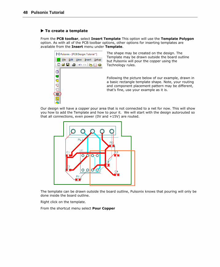
From the PCB toolbar, select Insert Template This option will use the Template Polygon option. As with all of the PCB toolbar options, other options for inserting templates are available from the Insert menu under Template.
The shape may be created on the design. The Template may be drawn outside the board outline but Pulsonix will pour the copper using the Technology rules.
Following the picture below of our example, drawn in a basic rectangle template shape. Note, your routing and component placement pattern may be different, that’s fine, use your example as it is.
Our design will have a copper pour area that is not connected to a net for now. This will show you how to add the Template and how to pour it. We will start with the design autorouted so that all connections, even power (0V and +15V) are routed.
The template can be drawn outside the board outline, Pulsonix knows that pouring will only be done inside the board outline.
Right click on the template.
From the shortcut menu select Pour Copper
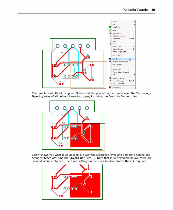
Pulsonix Tutorial 49
The template will fill with copper. Notice that the poured copper has obeyed the Technology Spacing rules of all defined items to copper, including the Board to Copper rules.
Below shows you what it would look like with the silkscreen layer and Template outline and Areas switched off using the Layers Bar (Ctrl-L). Note that in our example below, there are isolated islands retained. There are settings in the rules to also remove these if required.
50 Pulsonix Tutorial
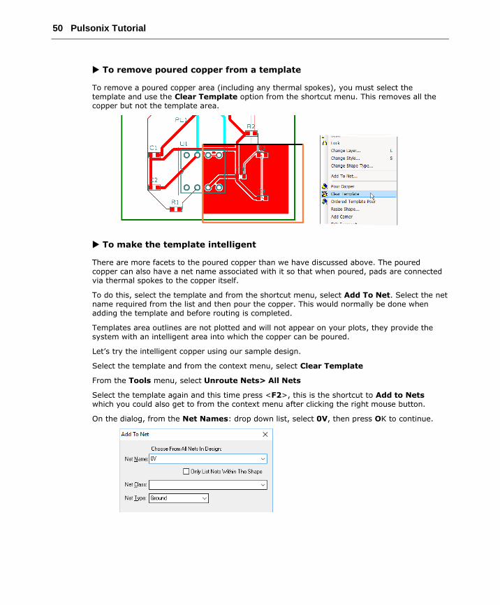
To remove poured copper from a template
To remove a poured copper area (including any thermal spokes), you must select the template and use the Clear Template option from the shortcut menu. This removes all the copper but not the template area.
To make the template intelligent
There are more facets to the poured copper than we have discussed above. The poured copper can also have a net name associated with it so that when poured, pads are connected via thermal spokes to the copper itself.
To do this, select the template and from the shortcut menu, select Add To Net. Select the net name required from the list and then pour the copper. This would normally be done when adding the template and before routing is completed.
Templates area outlines are not plotted and will not appear on your plots, they provide the system with an intelligent area into which the copper can be poured.
Let’s try the intelligent copper using our sample design.
Select the template and from the context menu, select Clear Template
From the Tools menu, select Unroute Nets> All Nets
Select the template again and this time press <F2>, this is the shortcut to Add to Nets which you could also get to from the context menu after clicking the right mouse button.
On the dialog, from the Net Names: drop down list, select 0V, then press OK to continue.
Pulsonix Tutorial 51
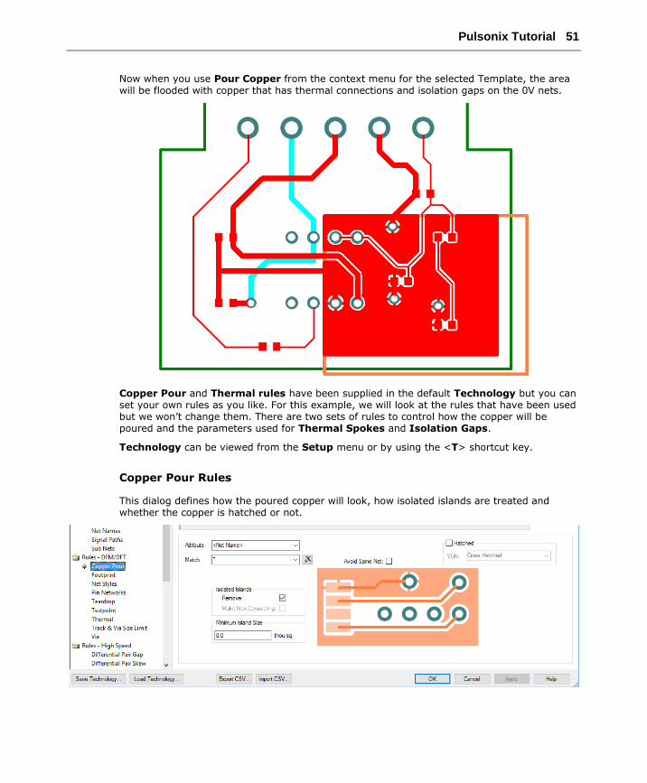
Now when you use Pour Copper from the context menu for the selected Template, the area will be flooded with copper that has thermal connections and isolation gaps on the 0V nets.
Copper Pour and Thermal rules have been supplied in the default Technology but you can set your own rules as you like. For this example, we will look at the rules that have been used but we won’t change them. There are two sets of rules to control how the copper will be poured and the parameters used for Thermal Spokes and Isolation Gaps.
Technology can be viewed from the Setup menu or by using the <T> shortcut key.
Copper Pour Rules
This dialog defines how the poured copper will look, how isolated islands are treated and whether the copper is hatched or not.

52 Pulsonix Tutorial
Thermal rules
This dialog defines the rules once the copper has been poured. Rules such as the number and size of the thermal spokes and isolation gaps, the start angle of the spokes, how thermal spokes are added to surface mount pads, vias and how the pads will be treated.
With additional rules now defined, the copper pour area in the Template could be repoured to look like this:
Pulsonix Tutorial 53
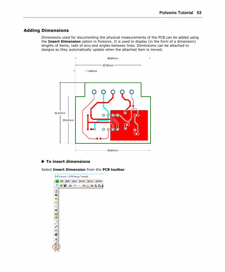
Adding Dimensions
Dimensions used for documenting the physical measurements of the PCB can be added using the Insert Dimension option in Pulsonix. It is used to display (in the form of a dimension) lengths of items, radii of arcs and angles between lines. Dimensions can be attached to designs so they automatically update when the attached item is moved.
To insert dimensions
Select Insert Dimension from the PCB toolbar.
54 Pulsonix Tutorial
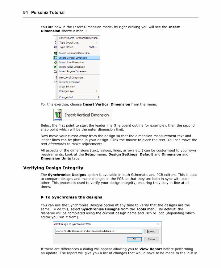
You are now in the Insert Dimension mode, by right clicking you will see the Insert Dimension shortcut menu:
For this exercise, choose Insert Vertical Dimension from the menu.
Select the first point to start the leader line (the board outline for example), then the second snap point which will be the outer dimension limit.
Now move your cursor away from the design so that the dimension measurement text and leader lines can be placed in your design. Click the mouse to place the text. You can move the text afterwards to make adjustments.
All aspects of the dimensions (text, values, lines, arrows etc.) can be customised to your own requirements. Look at the Setup menu, Design Settings, Default and Dimension and Dimension Units tabs.
Verifying Design Integrity
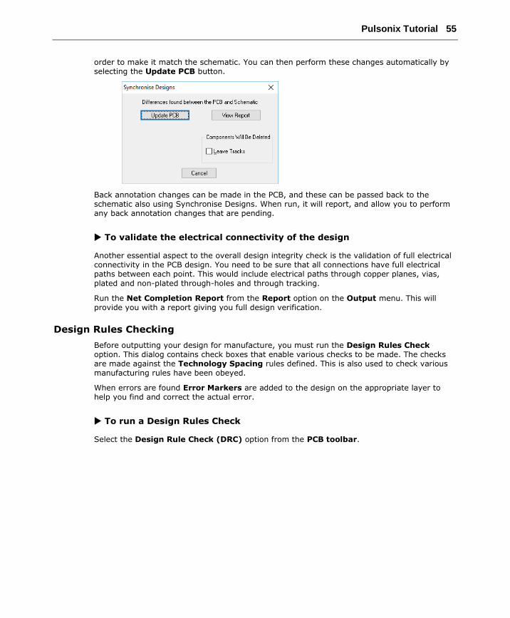
The Synchronise Designs option is available in both Schematic and PCB editors. This is used to compare designs and make changes in the PCB so that they are both in sync with each other. This process is used to verify your design integrity, ensuring they stay in-line at all times.
To Synchronise the designs
You can use the Synchronise Designs option at any time to verify that the designs are the same. To do this, select Synchronise Designs from the Tools menu. By default, the filename will be completed using the current design name and .sch or .pcb (depending which editor you run it from).
If there are differences a dialog will appear allowing you to View Report before performing an update. The report will give you a list of changes that would have to be made to the PCB in
Pulsonix Tutorial 55
order to make it match the schematic. You can then perform these changes automatically by selecting the Update PCB button.
Back annotation changes can be made in the PCB, and these can be passed back to the schematic also using Synchronise Designs. When run, it will report, and allow you to perform any back annotation changes that are pending.
To validate the electrical connectivity of the design
Another essential aspect to the overall design integrity check is the validation of full electrical connectivity in the PCB design. You need to be sure that all connections have full electrical paths between each point. This would include electrical paths through copper planes, vias,
plated and non-plated through-holes and through tracking.
Run the Net Completion Report from the Report option on the Output menu. This will provide you with a report giving you full design verification.
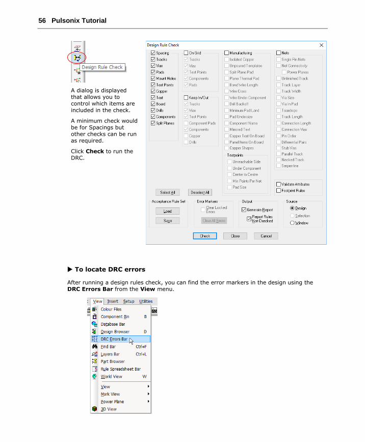
Design Rules Checking
Before outputting your design for manufacture, you must run the Design Rules Check option. This dialog contains check boxes that enable various checks to be made. The checks are made against the Technology Spacing rules defined. This is also used to check various manufacturing rules have been obeyed.
When errors are found Error Markers are added to the design on the appropriate layer to help you find and correct the actual error.
To run a Design Rules Check
Select the Design Rule Check (DRC) option from the PCB toolbar.
56 Pulsonix Tutorial
A dialog is displayed that allows you to control which items are included in the check.
A minimum check would be for Spacings but other checks can be run as required.
Click Check to run the DRC.
To locate DRC errors
After running a design rules check, you can find the error markers in the design using the DRC Errors Bar from the View menu.
Pulsonix Tutorial 57
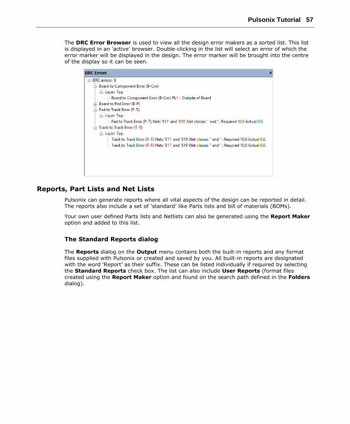
The DRC Error Browser is used to view all the design error makers as a sorted list. This list is displayed in an 'active' browser. Double-clicking in the list will select an error of which the error marker will be displayed in the design. The error marker will be brought into the centre of the display so it can be seen.
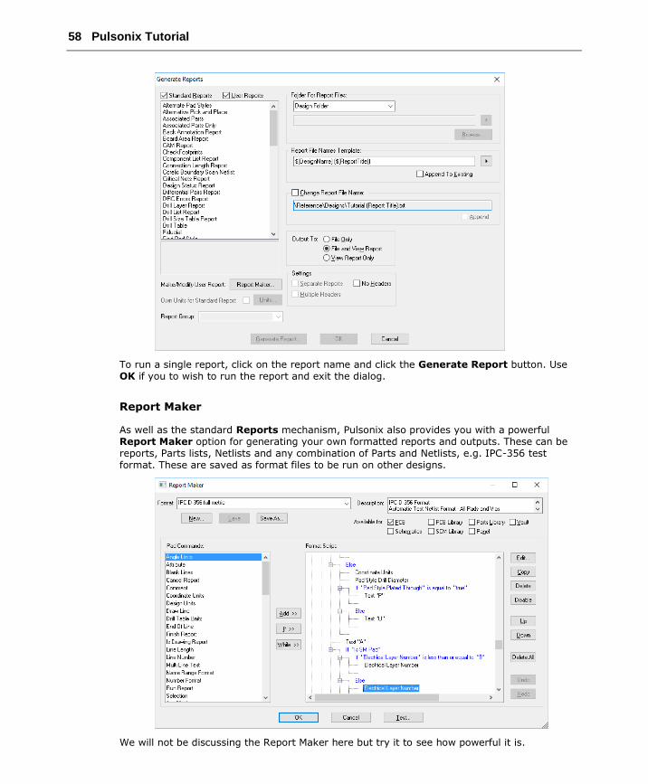
Reports, Part Lists and Net Lists
Pulsonix can generate reports where all vital aspects of the design can be reported in detail. The reports also include a set of ‘standard’ like Parts lists and bill of materials (BOMs).
Your own user defined Parts lists and Netlists can also be generated using the Report Maker option and added to this list.
The Standard Reports dialog
The Reports dialog on the Output menu contains both the built-in reports and any format files supplied with Pulsonix or created and saved by you. All built-in reports are designated with the word ‘Report’ as their suffix. These can be listed individually if required by selecting the Standard Reports check box. The list can also include User Reports (format files created using the Report Maker option and found on the search path defined in the Folders dialog).
58 Pulsonix Tutorial
To run a single report, click on the report name and click the Generate Report button. Use OK if you to wish to run the report and exit the dialog.
Report Maker
As well as the standard Reports mechanism, Pulsonix also provides you with a powerful Report Maker option for generating your own formatted reports and outputs. These can be reports, Parts lists, Netlists and any combination of Parts and Netlists, e.g. IPC-356 test format. These are saved as format files to be run on other designs.
We will not be discussing the Report Maker here but try it to see how powerful it is.
Pulsonix Tutorial 59
Plotting the Design
Pulsonix provides you with an output mechanism for generating professional PCB layout plots for manufacturing. All the plot and drilling outputs are located in one easy to use dialog, delivered in one button press once set up.
From this option you can select the layer or combinations of layers to plot. You can also set the scale, rotation, the position on the plot and the output driver.
From Pulsonix you can output:
• Gerber RS-274-D and RS-274-X (extended Gerber format) format photo-plots
• Windows printer plots using any installed Windows driver
• Active PDF prints
• Numerically controlled drilling (NC Drill) information (Excellon, Seib & Myer etc.)
• IPC-2581 format
• ODB++ format
• HPGL Pen plots
• IPC-D-356 Testpoint output
• JTAG boundary scan output
• GenCAD and UniDAT output
• Hyperlynx output
• LPKF prototype drilling output
• STEP and IGES mechanical CAD files
• DXF and IDF format files
• Output files for Bill Of Materials (BOM), assembly and pick & place machines
• User-defined files (parts lists and netlists) created in the Report Maker option
Plot types
Plots are available for all aspects of the design but because Pulsonix uses a configurable output mechanism, it means that any plot required can be generated:
• Top, bottom and inner electrical signal layers
• Silk screen layers
• Solder resist plots
• Solder paste masks
• Copper and power plane (full or split) layers
• Assembly and manufacturing drawings
• Drill letter/symbol drawings
• NC Drilling and profiling/routing files
• Inner, embedded component layers
60 Pulsonix Tutorial
To output plots
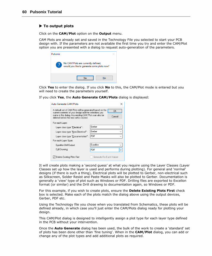
Click on the CAM/Plot option on the Output menu.
CAM Plots are already set and saved in the Technology File you selected to start your PCB design with. If the parameters are not available the first time you try and enter the CAM/Plot option you are presented with a dialog to request auto-generation of the parameters.
Click Yes to enter the dialog. If you click No to this, the CAM/Plot mode is entered but you will need to create the parameters yourself.
If you click Yes, the Auto Generate CAM/Plots dialog is displayed:
It will create plots making a ‘second guess’ at what you require using the Layer Classes (Layer Classes set up how the layer is used and performs during plotting). For general and ‘normal’ designs (if there is such a thing), Electrical plots will be plotted to Gerber, non-electrical such as Silkscreen, Solder Resist and Paste Masks will also be plotted to Gerber. Documentation is generally a ‘view’ type of plot such as Windows or PDF. Drilling files are exported to Excellon format (or similar) and the Drill drawing to documentation again, so Windows or PDF.
For this example, if you wish to create plots, ensure the Delete Existing Plots First check box is selected. Make each of the plots match the dialog above using the output devices, Gerber, PDF etc.
Using the Technology file you chose when you translated from Schematics, these plots will be defined already, in which case you’ll just enter the CAM/Plots dialog ready for plotting your design.
This CAM/Plot dialog is designed to intelligently assign a plot type for each layer type defined in the PCB without your intervention.
Once the Auto Generate dialog has been used, the bulk of the work to create a ‘standard’ set of plots has been done other than 'fine tuning'. When in the CAM/Plot dialog, you can add or change any of the plot types and add additional plots as required.
Pulsonix Tutorial 61
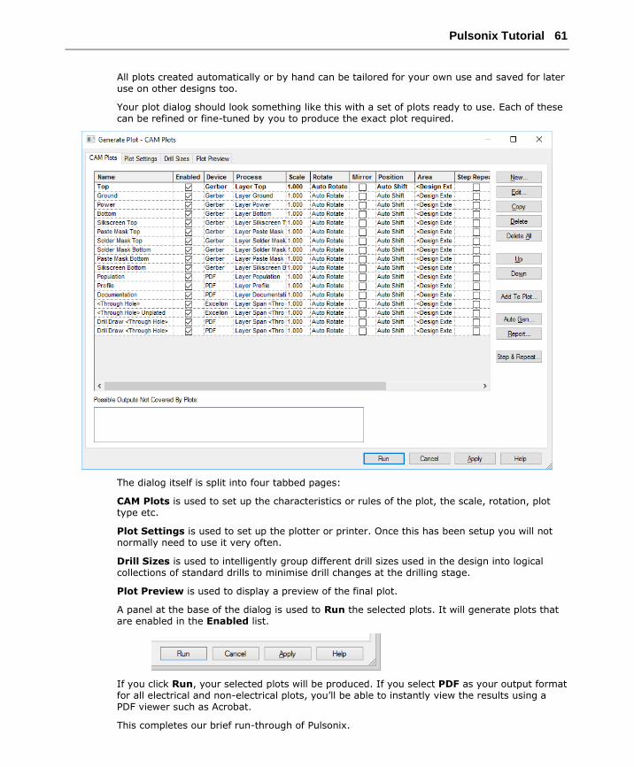
All plots created automatically or by hand can be tailored for your own use and saved for later use on other designs too.
Your plot dialog should look something like this with a set of plots ready to use. Each of these can be refined or fine-tuned by you to produce the exact plot required.
The dialog itself is split into four tabbed pages:
CAM Plots is used to set up the characteristics or rules of the plot, the scale, rotation, plot type etc.
Plot Settings is used to set up the plotter or printer. Once this has been setup you will not normally need to use it very often.
Drill Sizes is used to intelligently group different drill sizes used in the design into logical collections of standard drills to minimise drill changes at the drilling stage.
Plot Preview is used to display a preview of the final plot.
A panel at the base of the dialog is used to Run the selected plots. It will generate plots that are enabled in the Enabled list.
If you click Run, your selected plots will be produced. If you select PDF as your output format for all electrical and non-electrical plots, you’ll be able to instantly view the results using a PDF viewer such as Acrobat.
This completes our brief run-through of Pulsonix.

62 Pulsonix Tutorial
Additional Information
There are many more aspects to Pulsonix which are not covered in this document. Further information can be obtained in the Online Help using the <F1> key at any time, or from the Pulsonix Users Guide supplied as a PDF file under the Help menu and Online Manuals> or on our web site.
While evaluating Pulsonix or once you’ve purchased it, technical support is provided in the form of telephone support from our office or from your local sales office, or by email.
Head office support +44 (0)1684 296 570
Head office email support [email protected]
Web site www.pulsonix.com