Introducing PhoeniX Software solutions for … PhoeniX Software solutions for photonic chip design...
51
Introducing PhoeniX Software solutions for photonic chip design PRESENTED BY TWAN KORTHORST, CEO COLUMBIA UNIVERSITY, NYC, USA, OCTOBER 2015
Transcript of Introducing PhoeniX Software solutions for … PhoeniX Software solutions for photonic chip design...

Introducing PhoeniX Software solutionsfor
photonic chip design
P R E S E N T E D BY T WA N KO R T H O R S T, C EO
C O LU M B I A U N I V E RS I T Y, N YC , U S A , O C TO B E R 2 0 1 5

(C) 2015. ALL RIGHTS RESERVED. PHOENIX SOFTWARE. 2
PhoeniX Software Team
Sesilia Kriswandhi• Head of technical marketing, training and customer support
• Developing PhoeniX Software’s training program for 10 years now
Pietro Contu (Application Engineer – PIC design)
Remco Stoffer (Product Specialist – Design Solutions)
Twan Korthorst (CEO)
And Arjen, Jan, Imma, Bowen, Rino, Katrin, Sami, Anke, Niels, Marco, Remco Sol, Hossein, Arnout, Francesc, Erik, Gary, Vivian, Lioba, Erwin, Luis, Bart, Saeed, Jie, …..

(C) 2015. ALL RIGHTS RESERVED. PHOENIX SOFTWARE.
• While still dynamic (eg. GaN), electronics market is mature• Total electronic components market is > 500B$, with IC’s ~250B$
• Electronics Design Automation (EDA) market just under 10B$
• Mature silicon electronics industry comes with• Good array of foundries (TSMC, GF, Jazz, IBM, etc.)
• Mature EDA industry (Synopsys, Cadence, Mentor)
• Process Design Kits
• Existing technologies are reaching bandwidth limitations• Power consumption (heat) dominated by data transfer rather than computing
• Density
3
Electronic IC industry is steadily growing, but ‘big data’ is getting bigger by the second

(C) 2015. ALL RIGHTS RESERVED. PHOENIX SOFTWARE.
• Market need drives transition to integrated photonics solutions• Datacenters and High Performance Computing
• 40G/100G/400G, FTTH
• Microwave photonics (5G, nextgen wifi, LiDAR, …)
• (Bio-)sensing
• Photonic Integrated Circuit market today relatively small (220M$) • Market size x4 by 2019, still only 0,4% of global IC market size
• Mainly InP based, performance driven
• Silicon photonics enables the transition by leveraging silicon electronics technology • Cost effective manufacturing
• Functions integration
• High density
• Photonics technology is considered to be strategically important• Multiple Billion$ value in ‘transactions & investments’ recently
• Photonics will be a significant part of the electronic IC market
4
Photon will replace the electronand silicon photonics is well positioned to support this transition

(C) 2015. ALL RIGHTS RESERVED. PHOENIX SOFTWARE.
• Fabrication: thin film technologies, lithography, cleanrooms
• Design flow: verified mask layout design as final step
• Photonics is where electronics was in the 80’s• Transition from PCB to (silicon) IC
• Large number of (small) fabs providing manufacturing capacity
• Many software suppliers, each covering parts of the design flow
• Emerging standardization in processes and tools
5
There are many similaritiesbetween electronics & photonics industry

(C) 2015. ALL RIGHTS RESERVED. PHOENIX SOFTWARE.
• Wide variety of materials and technologies• Si / SOI, InP / III-V, PLC, TriPleX / SiN, LiNbO3, Polymers, …
• Hybrids, 3D stacking, SiP
• Scalability roadmap is unknown• Typical line-widths: 0.15 – 4 micrometer
• Number of components: 10’s – 1000’s per chip (relates to 10k – 1M primitives)
• RF-like or analog behavior (Telecom C-band is 1530 – 1565 nm ~ 193 THz)
• Design closely related with fabrication
• Process and temperature dependencies
6
With some key differences:photonics industry today is dynamic and fragmented

(C) 2015. ALL RIGHTS RESERVED. PHOENIX SOFTWARE. 7
There are many similaritiesbetween electronic & photonic IC design
with some key requirements for photonics design:
• Dedicated simulation tools• All angle layout• “Phase aware” routing• Special features for verification
Analog design time syndrome
“for a 10% analog 90% digital IC, the analog design takes 90% of the design time”

(C) 2015. ALL RIGHTS RESERVED. PHOENIX SOFTWARE.
• The analog ‘design time syndrome’ needs to be dealt with• PhoeniX Software’s unique photonic building block platform
enables real Photonic Synthesis, improving design efficiency
• Photonics process dependency needs to be handled• Integrated design platform to design for manufacturability
• PhoeniX Software introduced Process Design Kits in photonics in 2007
• In a scattered tooling landscape, a common interface is needed• PhoeniX Software co-founded the PDAFlow foundation in 2013
• All photonics software vendors are member
• De-facto standard for PDKs & tool interoperability
Shaping the photonics industryrole of PhoeniX Software
8

(C) 2015. ALL RIGHTS RESERVED. PHOENIX SOFTWARE. 9
PhoeniX Software’s mission• Supporting customers worldwide to
• Enhance research, process and product development
• Improve quality and reduce time to market
• Obtain a “first time right” and “design for manufacturability” infrastructure
• By offering• A unique highly integrated mask layout, process flow design and simulation
environment
• The only dedicated technology knowledge base and MES for the market
• Process Design Kits for foundry access
• Targeted training courses and customer support

(C) 2015. ALL RIGHTS RESERVED. PHOENIX SOFTWARE. 10
PhoeniX Software• Founded in 2003, history going back to 1991
• Focus on software solutions for manufacturability: design instead of simulations
• Located in Enschede, The Netherlands
• Presence in: China, Japan, India, Korea, Israel, USA, UK, Portugal & Spain, Germany
• Customers ranging from R&D to manufacturing, from large OEMs and start-upsto universities and research institutes
• Design solutions • OptoDesigner 5, integrated suite for photonics chip design
• MaskEngineer, FlowDesigner for MEMS, microfluidics, printed electronics, …
• Reselling CleWin (layout editor) and ASPIC (photonics circuit design)
• Manufacturing automation• Living Database, R&D and low volume MES

(C) 2015. ALL RIGHTS RESERVED. PHOENIX SOFTWARE. 11
PhoeniX Software’s vision
“Integrated photonics research and product development require an integrated and flexible workflow: the integrated
Product Creation process (iPCP)”

(C) 2015. ALL RIGHTS RESERVED. PHOENIX SOFTWARE. 12
Remember: photonics ≠ CMOS electronics• Integrated Photonics has “RF-like” or “analog”behavior, requiring:
• Accurate and flexible definition of all angle shapes
• Control of phase relations
• Dedicated photonics simulation routines
• Libraries with parametric photonic cells
• Special features for verification (DRC, LVS)

(C) 2015. ALL RIGHTS RESERVED. PHOENIX SOFTWARE.
• Chip and mask layout• Extensive built-in libraries for photonic elements and devices
• Photonic Synthesis based on technology parameters and design intent
• Verification, DRC and Routing (electrical, optical, constraint based, …)
• Photonic simulations• Circuit Simulations (by ASPIC, or internal solvers)
• Mode-solvers and Propagation Simulations
• Active Devices Simulations
• Process Flow Visualization
• Flexible Import and Export capabilities• 3rd party tool integration: circuit tools from Lumerical, VPIphotonics and Photon Design
• Easy to use GUI including proprietary PHX scripting
• Compatible with Process Design Kits (PDKs)
13
OptoDesigner 5, photonic chip design suite

(C) 2015. ALL RIGHTS RESERVED. PHOENIX SOFTWARE. 14
OptoDesigner 5, chip and mask layout• Object oriented parametric mask design environment
• Relative connectivity of elements
• Complete parametrized library for photonics
• Define custom layouts as new elements
• Optimization algorithms, eg. to get optical path length
• Automation for routing, verification, DRC and mask assembly
• Integrated with physical simulation capabilities (mode-solvers and propagation simulation)
• Native all angle and all shape design• Maintaining design intent as long as possible
• Automatic GDS compiler, controlling discretization errors
• Powerful domain specific scripting capabilities• Fast: kernel written in C++
• Mature and simple syntax: dedicated to photonic chip design

(C) 2015. ALL RIGHTS RESERVED. PHOENIX SOFTWARE.
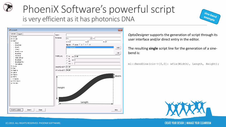
• Photonic chip designs are created from “primitives” or photonics elements
• Example shows a sine-bend, defined by the width of the waveguide and the distance between the input and output in vertical and horizontal direction
15
OptoDesigner 5, chip and mask layout
Some examples of elements in the standard library:
CurvedWire, Polygon, RectangleRounded, Straight, StraightOffset, Wire, WireRoute, Yblunt, BendEllipse, Circle, CircleSegment, Donut, Ellipse, EllipseSegment, EllipseSliced, Bend, BendCosine, BendEuler, BendPolar, BendS, BendSine, …
Any shape you can describe mathematically can be used as well

(C) 2015. ALL RIGHTS RESERVED. PHOENIX SOFTWARE.
• Photonics elements are combined into devices
• Example shows a Mach-Zehnder interferometer, created out of 4 (or 12) elements
• Connectivity is important, in case you want to make changes. For instance to introduce a phase (read length) difference between the two arms
16
Snapshot of devices in the photonics library:
DirectionalCoupler, MMI1xN, MMI2xN, MMIMxN, StarCoupler, StarCouplerMxN, ModeSplitter, Sjunction, StarBase, ArcLens, EllipticalLens, HyperbolicLens, SpiralSegment, SpiralSegmentInOut, …
If you create your own device you can easily add it to the library
OptoDesigner 5, chip and mask layout

(C) 2015. ALL RIGHTS RESERVED. PHOENIX SOFTWARE.
Generic (EDA) scripting languagesdon’t understand photonics and are inefficient
Example of the description of a sine-bend taken from a Cadence Virtuoso (SKILL) p-cell as used in a silicon photonics PDK
Same applies to Mentor Graphics AMPLEOr generic languages like Matlab, Python, Ruby, …
(C) 2015. ALL RIGHTS RESERVED. PHOENIX SOFTWARE.
PhoeniX Software’s powerful scriptis very efficient as it has photonics DNA
OptoDesigner supports the generation of script through its user interface and/or direct entry in the editor.
The resulting single script line for the generation of a sine-bend is:
ml::BendSine(cin->[0,0]: wfix(Width), Length, Height);

(C) 2015. ALL RIGHTS RESERVED. PHOENIX SOFTWARE.
OptoDesigner supports the generation of script through its user interface and/or direct entry in the editor.
The resulting single script line for the generation of a sine-bend is:
ml::BendSine(cin->[0,0]: wfix(Width), Length, Height);
parameters
PhoeniX Software’s powerful scriptis very efficient as it has photonics DNA

(C) 2015. ALL RIGHTS RESERVED. PHOENIX SOFTWARE.
OptoDesigner supports the generation of script through its user interface and/or direct entry in the editor.
The resulting single script line for the generation of a sine-bend is:
ml::BendSine(cin->[0,0]: wfix(Width), Length, Height);
relative connectivity
PhoeniX Software’s powerful scriptis very efficient as it has photonics DNA

(C) 2015. ALL RIGHTS RESERVED. PHOENIX SOFTWARE.
OptoDesigner supports the generation of script through its user interface and/or direct entry in the editor.
The resulting single script line for the generation of a sine-bend is:
ml::BendSine(cin->[0,0]: wfix(Width), Length, Height);
width profile
PhoeniX Software’s powerful scriptis very efficient as it has photonics DNA

(C) 2015. ALL RIGHTS RESERVED. PHOENIX SOFTWARE.
PhoeniX Software’s powerful scriptis very efficient as it has photonics DNA
Several options for the width profile exist: fixed, linearly changing, exponentially changing, parabolicly changingand even arbitrary functionally changing.
And … the conversion of the intended shape to discretized polygons with a user defined maximum error to the idealpath in the final mask file is fully automated!
Note: instead of the built-in sine-bend any arbitrary self defined function can be used as well, like:
ml::CenterPath( cin->[0,0] : {t->t*Length,-0.5*Height*cos(t*pi)}, wfix(Width));
wfix wlin wexp wpar

(C) 2015. ALL RIGHTS RESERVED. PHOENIX SOFTWARE. 23
OptoDesigner 5, photonic simulationsAdvanced Simulation for Photonics Integrated Circuits (ASPIC)
• Allows analysis of larger / more complex circuits
• Much faster than electromagnetic simulator
• Especially useful for optimizing performance & yield
• Response in spectral domain• Calculates amplitude, phase, group delay, dispersion and polarization
• Large library of components• Waveguides, bends, MMI’s, rings, DC, splitter, MZ, phase modulator, crossings, …
• Works with PDKs
• Integration with OptoDesigner and Matlab

(C) 2015. ALL RIGHTS RESERVED. PHOENIX SOFTWARE. 24
OptoDesigner 5, photonic simulations
Photonic Mode Simulations• Advanced mode-solvers
• Film mode matching, finite difference
• Full vectorial, real/complex
• Thermo, Electro, Stress optical effects
• 3D Ring resonator module (3D CMT)
Photonic Propagation Simulations• BPM, BEP/EME, FDTD
• Zone & FAST
• Integrated with layout

(C) 2015. ALL RIGHTS RESERVED. PHOENIX SOFTWARE. 25
OptoDesigner 5, process flow design• Visualize fabrication process steps
• Based on process flow• Visualize cross section• Shows intermediate steps
• Library of recipes and models• Isotropic, Directional, Anisotropic, Lift-off, CMP, Wafer bonding• Parametric Analytical models• Materials, Etchants and Rates
• Benefits• Essential for process development, supporting documentation• Avoids costly mistakes, improves yield

(C) 2015. ALL RIGHTS RESERVED. PHOENIX SOFTWARE.
• Layout and simulations in one environment
• Relative connectivity of design elements
• Applies technology information (from a PDK or library)
• Optimization routines
• Photonics DNA• Easy to use GUI with powerful domain specific scripting
• Large set of generic photonic building blocks
OptoDesigner’s Building Block platformprovides the ability to automatically generate designs

(C) 2015. ALL RIGHTS RESERVED. PHOENIX SOFTWARE.
Ease of design through Photonic Synthesis enabled by PhoeniX Software’s photonic building block platform
27
In integrated photonics there is some emerging standardization in materials and processes, however today it is dynamic and diverse:
• New materials will be introduced• Process changes will happen• Designs being ported from R&D
into volume
Hence the need for a structuredand flexible design environment, focused on manufacturability

(C) 2015. ALL RIGHTS RESERVED. PHOENIX SOFTWARE.
Ease of design through Photonic Synthesis enabled by OptoDesigner’s photonic building block platform
Photonics building block:
• Translates design intent into DRC clean layout• Design intent can be either optically or
geometrically defined• Ability to handle wide parameter range• Incorporates process information
Example:Arrayed waveguide grating (AWG),widely used as optical mux/demux

(C) 2015. ALL RIGHTS RESERVED. PHOENIX SOFTWARE.
Ease of design through Photonic Synthesis enabled by OptoDesigner’s photonic building block platform
29
From design intent to final mask layout:
• Calculating the required shapes, given the design intent and the fabrication information
• Turning these into polygons, given a maximum allowed path error
• Placing the polygons into the required mask layers, including sizing, inversion, booleanoperations, etc.
• Checking design rules• Exporting mask (GDS2) files
AWG example: from intended waveguide or “logical” design into actual mask or “GDS” design to fabricate with the correct waveguide dimensions (cross section)

(C) 2015. ALL RIGHTS RESERVED. PHOENIX SOFTWARE.
Ease of design through Photonic Synthesis enabled by OptoDesigner’s photonic building block platform
Example: optical delay-line, implemented as spiral

(C) 2015. ALL RIGHTS RESERVED. PHOENIX SOFTWARE.
• A “90 degree optical hybrid” is a key component for optical receivers
• Purpose is to measure the phase difference between two optical signals, by converting the optical signals into electrical signals representing the Re and Im parts of the complex amplitude difference
• Applied to reconstruct complex phase modulated signals(like DQPSK en 16QAM)
Ease of design through Photonic Synthesis enabled by OptoDesigner’s photonic building block platform

(C) 2015. ALL RIGHTS RESERVED. PHOENIX SOFTWARE.
• A “90 degree optical hybrid” building block contains splitters, crossings, combiners, detectors and connecting waveguides
Yohei Sakamaki, Takeshi Kawai, Tetsuro Komukai, Mitsunori Fukutoku, Tomoyoshi Kataoka, Toshio Watanabe, Yuzo Ishii, "Experimental demonstration of multi-degree colorless, directionless, contentionless ROADM for 127-Gbit/s PDM-QPSK transmission system" Opt. Express 19, B1-B11 (2011)
“Monolithically integrated dual-quadrature receiver on InP with 30 nm tunable local oscillator”, Kimchau N. Nguyen et al., OSA 2011, December 2011 / Vol. 19, No. 26 / OPTICS EXPRESS B716
Ease of design through Photonic Synthesis enabled by OptoDesigner’s photonic building block platform

(C) 2015. ALL RIGHTS RESERVED. PHOENIX SOFTWARE.
Ease of design through Photonic Synthesis enabled by OptoDesigner’s photonic building block platform
Example: 90 degree hybrid, including 1-symbol delay
The path length difference ∆𝐿 in the 90 degree hybrid Building Block depends on the used photonic technology:
∆𝐿 = 𝜆4 𝑛𝑔
,
where 𝜆 is the wavelength and 𝑛𝑔 is the group index of the used
waveguide.

(C) 2015. ALL RIGHTS RESERVED. PHOENIX SOFTWARE.
• The MMI’s, crossings and detectors can be picked from the design library and placed into the layout at the required locations
• As the connecting waveguides are constraint based, special care is required when designing these• Depending on the fabrication technology and waveguide geometry (cross section) the actual
routing needs to be calculated and implemented
• The optical path lengths of the connecting waveguides need tomatch, including a 90degree phase shift, given the positions of the input and output ports of all the individual components
Ease of design through Photonic Synthesis enabled by OptoDesigner’s photonic building block platform

(C) 2015. ALL RIGHTS RESERVED. PHOENIX SOFTWARE.
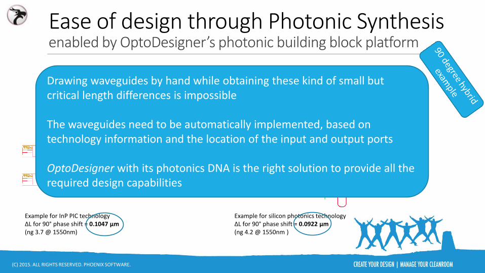
• Matching the waveguides optical path lengths requires• Ability to calculate (or simulate) and use the optical properties of a waveguide (group index)
• Relative connectivity, to solve the netlist of the connecting waveguides between all the components, and to allow for making changes easily
The path length difference ∆L for a 90 degree phase shift is determined by the technology. Therefore, ∆L should not change if the imposed constraints of the Building Blocks changes, such as the distances between its output ports.
Ease of design through Photonic Synthesis enabled by OptoDesigner’s photonic building block platform
gap = 110 umgap = 170 um

(C) 2015. ALL RIGHTS RESERVED. PHOENIX SOFTWARE.
• Matching the optical path lengths requires• Ability to calculate (or simulate) and use the optical properties of a waveguide (group index)
• Relative connectivity, to solve the netlist of the connecting waveguides between all the components, and to allow for making changes easily
Example for silicon photonics technology∆L for 90° phase shift = 0.0922 µm(ng 4.2 @ 1550nm )
Example for InP PIC technology∆L for 90° phase shift = 0.1047 µm(ng 3.7 @ 1550nm)
Ease of design through Photonic Synthesis enabled by OptoDesigner’s photonic building block platform
(C) 2015. ALL RIGHTS RESERVED. PHOENIX SOFTWARE.
• Matching optical path lengths requires• Ability to calculate (or simulate) and use the optical properties of a waveguide
• Relative connectivity, to solve the netlist of the connecting waveguides between all the components, and to allow for making changes easily
Example for silicon photonics technology∆L for 90° phase shift = 0.0922 µm(ng 4.2 @ 1550nm )
Example for InP PIC technology∆L for 90° phase shift = 0.1047 µm(ng 3.7 @ 1550nm)
Drawing waveguides by hand while obtaining these kind of small but critical length differences is impossible
The waveguides need to be automatically implemented, based on technology information and the location of the input and output ports
OptoDesigner with its photonics DNA is the right solution to provide all the required design capabilities
Ease of design through Photonic Synthesis enabled by OptoDesigner’s photonic building block platform

(C) 2015. ALL RIGHTS RESERVED. PHOENIX SOFTWARE. 38
Available PDKs for PhoeniX Software• Silicon Photonics: IMEC, CEA-Leti, VTT and IHP
• InP: FhG/HHI, Oclaro and SMART Photonics
• TriPleX (SiN): LioniX
• Packaging: Gooch&Housego, Linkra, XiO Photonics,Tyndall, Technobis ipps, Chiral Photonics
More than 300 designs created and fabricated in MPW’s with our tools in the last 3 years!

(C) 2015. ALL RIGHTS RESERVED. PHOENIX SOFTWARE. 39
PhoeniX Software actively collaboratesby co-founding the PDAFlow foundation in 2013
PDAFlow eco-system: software vendors collaborating to improve design flows

(C) 2015. ALL RIGHTS RESERVED. PHOENIX SOFTWARE.
PhoeniX Software is playing a central roleto create more integrated design flows, including EDA oriented
40
In addition to a PhoeniX based design flow
• Centered around (PDAFlow) PDKs and core capabilities of the PhoeniX Software platform
• Enabling schematic capture in a PDA or EDA tool and hand-over to OptoDesignerfor layout implementation, routing and verification (DRC, connectivity)
• Curve handling and layout generation in OptoDesigner and writing to GDS or OA to integrate into EDA tools, like Virtuoso, L-Edit, Pyxis
• Provide additional curve information to support LVS with Calibre

(C) 2015. ALL RIGHTS RESERVED. PHOENIX SOFTWARE. 41
Collaboration and Standardization
PhoeniX Software collaborates with software vendors from photonics and electronics to improve design flows
PhoeniX Software co-founded with Photon Design and Filarete the PDAFlowfoundation, maintaining an open standard for tool interoperability and PDKs

(C) 2015. ALL RIGHTS RESERVED. PHOENIX SOFTWARE.
• Most of our customers use OptoDesigner stand-alone for PIC layout• Combination of MPW/external fab users as well as vertically integrated OEMs
• Includes DRC, connectivity checks and access to PDKs (external or internal)
• A part of these customers use our physical simulators• Mainly to support layout generation of functional (WDM, delays, phase matching) photonic structures
• We target simulation/calculation assisted layout generation, to turn design intent into manufacturable layout
• All relevant solvers are available in OptoDesigner
• Some customers create layout in OptoDesigner and import this (by means of a GDS file) into EDA tools• Especially traditionally IC oriented organizations, already making use of EDA mask layout solutions
42
Use case scenarios (1)

(C) 2015. ALL RIGHTS RESERVED. PHOENIX SOFTWARE.
• Traditional IC design tools are missing generic photonic elements and devices. There are some example libraries, but for actual design you need to start from scratch• This requires writing extensive scripts for a very large fraction of the design
• And photonics is non-Manhattan and requires all angle design features (location of ports, rotation, smooth curves, connectivity)
• Even when a PDK is available, you will need custom design of photonics• Eg. waveguide optical length matching / WDM components / filtering / …
• IMEC MPW coordinator Amit Khana: “…today 70% of the designs is full custom.”
• OptoDesigner provides all its native built-in photonics layout elements, devices, routing, simulations, …, capabilities stand-alone or in combination with tools from other vendors
• Using OptoDesigner saves time and money and decreases risk• CEA-Leti MPW coordinator Maryse Fournier: “We see directly when the design
is made with PhoeniX: very high quality, ready to fabricate.”
43
Use case scenarios (2)

(C) 2015. ALL RIGHTS RESERVED. PHOENIX SOFTWARE. 44
Use case scenarios (3)• PhoeniX Software’s Photonic Building Block platform allows for design modules to be
developed and provided (targeting configurable photonic devices)
BrightAWG module

(C) 2015. ALL RIGHTS RESERVED. PHOENIX SOFTWARE. 45
Use case scenarios (3)• PhoeniX Software’s Photonic Building Block platform allows for design modules to be
developed and provided (targeting configurable photonic devices)
BrightAWG module
There is not a commercially available alternative for layout implementation of complex photonic devices and structures, with a proven track record and compatible with any
PIC fabrication technology (silicon photonics, InP, silicon nitride, TriPleX, LiNBO3, PLC, polymer, …)
Emil Kleijn, lead designer EFFECT Photonics “… it is currently the most capable tool for designing complicated masks for PICs.”

(C) 2015. ALL RIGHTS RESERVED. PHOENIX SOFTWARE. 46
Why use PhoeniX Software• We have been supporting 100’s of MPW-designers and vertically integrated
organizations getting started with PIC design
• More than 25 years photonics design and tools expertise, available trough excellent customer support• Our support is valued by our customers with a 9.1 out of 10
• By using a PDK (your own or from a fab partner), design times have gone down to weeks instead of months
• PDK set-up time for OptoDesigner takes hours to days, not weeks to months• We help our customers with training and support, including configuration and set-up of design libraries and
design flows
• Using OptoDesigner and the PhoeniX Software teamsaves time and money and decreases risk

(C) 2015. ALL RIGHTS RESERVED. PHOENIX SOFTWARE.
• PhoeniX Software• develops solutions focusing on design for manufacturability
• provides world-class training and support to photonics designers
• has a history going back to 1991 in integrated photonics
• serves more than 275, majority commercial, customers worldwide
• OptoDesigner• is the dominant commercial tool for photonics layout generation
• provides physical simulations and layout in one user friendly environment
• includes photonics verification and design rule checking
• interfaces with world-class circuit simulators
• enables EDA tools with mature and dedicated photonics capabilities
• gives access to 8 MPW photonic foundry PDKs
47
Summary

(C) 2015. ALL RIGHTS RESERVED. PHOENIX SOFTWARE.
• Free one month trial, including web-sessions
• Several licensing models
• Special offer for first time MPW users
• Join a MPW training at one of our 8 foundry partnershttp://www.phoenixbv.com/training
48
Engage with us

(C) 2015. ALL RIGHTS RESERVED. PHOENIX SOFTWARE.
• JePPIX training at University of Eindhoven (NL): 26 October - 6 November 2015• MPWs at FhG/HHI, Oclaro and SMART Photonics
• III-V photonics theory and fabrication (including practical work)
• Hands-on software training
• Europractice training at IMEC (Leuven, Belgium): 18 – 20 November 2015• MPWs at IMEC and CEA-Leti
• Silicon photonics technology and building blocks
• Hands-on software training
• LioniX webtrainings• Regular training opportunities for TriPleX (SiN) MPWs
• Technology and building blocks
• Software and PDK introduction
http://www.phoenixbv.com/training
49
Training opportunities

(C) 2015. ALL RIGHTS RESERVED. PHOENIX SOFTWARE.
• PIC training at Columbia University (New York, USA): 19 – 23 October 2015• All technologies, hands-on software, packaging and design services
• JePPIX training at University of Eindhoven (NL): 26 October - 6 November 2015• MPWs at FhG/HHI, Oclaro and SMART Photonics
• III-V photonics theory and fabrication (including practical work)
• Hands-on software training
• Europractice training at IMEC (Leuven, Belgium): 18 – 20 November 2015• MPWs at IMEC and CEA-Leti
• Silicon photonics technology and building blocks
• Hands-on software training
• LioniX webtrainings• Regular training opportunities for TriPleX (SiN) MPWs
• Technology and building blocks
• Software and PDK introduction
http://www.phoenixbv.com/training
50
Training opportunities

http://www.phoenixbv.com