InternationalWorkshop on Power Supplyon Chip 2012pwrsocevents.com/.../session-2/2.4_Khan.pdfSession...
18
Session 2: Power Semiconductor Technologies “PMIC technologies for integrated DC-DC converters” InternationalWorkshop on Power Supplyon Chip 2012 “PMIC technologies for integrated DC-DC converters” Tahir Khan Principal Member of Technical Staff Maxim Integrated
Transcript of InternationalWorkshop on Power Supplyon Chip 2012pwrsocevents.com/.../session-2/2.4_Khan.pdfSession...

Session 2: Power Semiconductor Technologies“PMIC technologies for integrated DC-DC converters”
International Workshop on Power Supply on Chip 2012
“PMIC technologies for integrated DC-DC converters”
Tahir Khan
Principal Member of Technical Staff
Maxim Integrated

Outline
• Application Overview
• Technology Node impact
• Device level innovation
• Summary

PMIC – building blocks
• Power management ICs are used to manage the accurate power flow in portable and handheld devices
• Power Management block is the biggest size hog on the IC and requires the most aggressive techniques to improve as we move ahead
POWER MANGEMENT CONTROL BLOCK
POWER MANGEMENT BLOCK
AUDIO Micro-USB
HAPTIC DRIVERDIGITAL CONTENT

Impact of technology node
• Digital footprint has seen a significant reduction as smaller technology node has a significant impact on individual transistor size
• A big factor which enables such a transition is the scaling of supply voltage which does not hold true of Power transistors

Comparison across technology node - PowerFET
• Taking the example of a standard 5Vsymmetric MOSFET over multipletechnology, the pitch of the device doesshrink with smaller technology node
• The minimum channel length does notshrink along with technology as thevoltage requirement is fixed and
Body/Source Drain
Gate
voltage requirement is fixed andreduction is a by product of other designrules
• There is something to be gained bytransitioning to smaller technology nodesfor consumer technologies which areutilize such FETs very extensively

Power Loss of MOSFETs
Synchronous Buck ConverterPower loss for Synchronous FET Q2:
PQ2=PCOND+PGD+POSS+PQrr
PCOND=Irms2RDS(ON)
PGD=QgVgfs
POSS= VinQOSSfs
PQrr=VinQrrfs
2
1
Power loss for Control FET Q1:
►Ron dominates total power loss at low frequencies
►Qg begins to dominates total power loss at high frequencies such as multi-megahertz
►FOM=Ron × Qg can be a simple indicator of converter efficiency
►Both Ron and Qg need to be minimized to achieve maximum efficiency
PQ1=PCOND+PSW+PGD+POSS
PCOND=Irms2RDS(ON)
PSW= Vin(Qgs/2+Qgd)fs
PGD=QgVgfs
POSS= VinQOSSfs
G
O
I
I
2
1

Innovative structures for improved performance
• Moving to smaller technology nodes(0.18um and below) also brings with itsome additional implants which arerequired for CMOS devices
• Such additional layers are viewed as ahindrance to migration to smaller nodes,but it also opens the door to innovativedevice designsdevice designs
• One such asymmetric MOSFET developedis shown on right which utilizes Haloimplants normally reserved for CMOSdevices
“Physics, Technology, and Modeling of Complementary Asymmetric MOSFETs” IEEE TRANSACTIONS ON ELECTRON DEVICES, VOL. 57, NO. 10 OCTOBER 2010

Utilizing small feature sizes – 90/65nm
• This novel structure details the path forward forPowerFET design in future BCD technologies
• The structure where active drift region issandwiched between Shallow trench isolation(STI) islands is shown to achieve more than 35Vbreakdown without any added processing steps
• This structure can only be built in 90nm• This structure can only be built in 90nmtechnology or below which allow small active-active spacing
“Innovative lateral field plates by gate fingers on STI regions in deep submicron CMOS “ Proceedings of the 20th International Symposium on Power
Semiconductor Devices & IC's
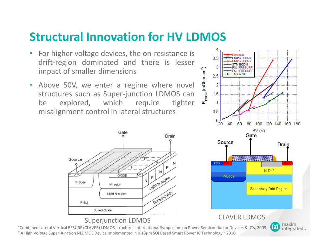
Structural Innovation for HV LDMOS
• For higher voltage devices, the on-resistance isdrift-region dominated and there is lesserimpact of smaller dimensions
• Above 50V, we enter a regime where novelstructures such as Super-junction LDMOS canbe explored, which require tightermisalignment control in lateral structures
Superjunction LDMOS CLAVER LDMOS
“Combined Lateral Vertical RESURF (CLAVER) LDMOS structure” International Symposium on Power Semiconductor Devices & IC's, 2009
“ A High Voltage Super-Junction NLDMOS Device Implemented in 0.13μm SOI Based Smart Power IC Technology “ 2010

Structural improvement in Qg
• Several structures have been developed to minimize Qg (especially Qgd) in LDMOS design to reduce switching losses
• For field-drift LDMOS devices, the solutions range from floating field plates to utilizing source field plate to minimize gate poly area
• For active drift devices, specifically LV FETs, stepped gate structure is an attractive candidate to minimize capacitanceattractive candidate to minimize capacitance
Stepped gate structure
“Planar Dual Gate Oxide LDMOS Structures in 180nm Power Management Technology” International Symposium on Power Semiconductor
Devices and Ics 2012

Safe Operating Area of LDMOS devices
• Efficient switching and robustness are key requirements of LDMOS devices integrated into BCD technologies
• To improve robustness of LDMOS devices, key feature is to degrade the parasitic bipolar which exists in parallel to the PowerFET
• The standard approach is to opt for a heavily doped body to reduce the base resistance and doped body to reduce the base resistance and delay the triggering of this bipolar
• Another approach is drain side engineering to reduce Kirk-effect related SOA degradation
Drain-side engineering Source-side engineering
ISPSD 2002 (Motorola) ISPSD 2005 (Texas Instruments)

SOA improvement for next generation
• To minimize additional processing steps to improve SOA of LDMOS devices, such as buried body implant, structural solution can be utilized to the same effect
• The dotted channel structure becomes an attractive candidate as we go to a smaller technology node with smaller contact size and design rules
Dotted channel length structure
“Rugged Dotted-channel LDMOS structure” International Electron Devices Meeting 2008

Integration Issues – Well Proximity Effect
• With significant space being utilized by analogFETs, merging of devices is of great importanceto achieve significant footprint reduction
• Reduced well enclosures work well for digitalCMOS devices but cannot be used as-is foranalog application due to well enclosure effects
IEEE CICC 2006, Freescale Semi

Integration Issues – STI proximity effect
• Another drawback of deep submicron technologies with STI defined active under non-uniform stress
• STI induces stress has shown to affect both VT and ID,sat of MOSFETs and special care must be taken for matched pairs with multiple schemes possible
IEEE CICC 2006, Freescale Semi

Other components - Bipolars
• Bipolar transistors are still heavily used in precision analog circuits where matching between pairs is of critical importance
• The devices are usually built out of available processing steps and are parasitic structures with no dedicated processing steps
• Gain of bipolars is crucial from application perspective with most of the latest technologies providing numbers ranging from 50-100latest technologies providing numbers ranging from 50-100

Other components - Resistors
• Resistors are very heavily utilized in analog and power circuits
• High sheet-rho, low temperature coefficient (T.C.) and good matching are key design parametric for these components
• Diffused well resistors are used for good matching applications while poly resistors are good for zero T.C. design
IEEE TED 2003 (NCK Univ Taiwan),

Other components - Capacitors
• Capacitors can occupy significant footprint on PMICs and multiple options are offered in technologies depending on trade-off vs. added cost
• Good linearity MIM caps have superior performance (density, voltage coefficient) vs. other options but they come with additional cost of dedicated processing steps
• One inexpensive alternative is the MOM cap which has lower density but is free of cost. The density is improving with each technology node with free of cost. The density is improving with each technology node with density approaching 1fF/um2 in latest technology node (90nm)
MIM cap

• With innovations in technology, significant reduction has been achieved for die footprint. Going to a smaller technology node can be justified with an increase in digital content on-chip which has the most significant impact of such a move
• A large chunk of area is now occupied by external passives where higher switching freq & on-die integration will make a much more significant impact
• Shrink in analog/power blocks is always challenging but with innovativestructures (e.g. zero channel length, DIELER), additional cost of processingsteps can be offset with improved performance
The path forward
structures (e.g. zero channel length, DIELER), additional cost of processingsteps can be offset with improved performance
Die Area