INTERNATIONAL JOURNAL OF RESEARCH REVIEW IN …ijrrest.org/issues/ijrrest_vol-4_issue-1_044.pdf ·...
12
IJRREST INTERNATIONAL JOURNAL OF RESEARCH REVIEW IN ENGINEERING SCIENCE & TECHNOLOGY (ISSN 2278 –6643) VOLUME-4, ISSUE-1, APRIL-2015 (Proceedings of “6 th National Conference on Make in India PMs Vision : Role of Engineering and Management Innovations to Achieve this Vision” Organised by Apex Group of Insti tutions, Karnal, Haryana, India, April-2015) 250 | Page | © IJRREST | http://ijrrest.org/issues/?page_id=12 REVIEW ON MICROSTRIP PATCH ANTENNA 1 Ritika Saini, 2 Vishal Girdhar 1 Assistant Professor, AIMT/ECE Department, Karnal, Haryana, India Email: [email protected] 2 Assistant Professor, AIMT/ECE Department, Karnal, Haryana, India Email:[email protected] Abstract— Microstrip Patch Antenna (MPA) is generally used in modern communication devices, and a large part of day-to-day communication is done through it. Study of literature of past few year shows that, the leading work on MPA is focused on designing compact sized broadband microstrip antenna. But inherently MPA have narrow bandwidth so to enhance bandwidth various techniques are engaged. In this paper we discuss the basics of microstrip antenna, various feeding techniques, design model, antenna parameters and techniques used to improve the bandwidth of antenna with their advantage and disadvantages. Keywords- Microstrip antenna, feed techniques, DGS. 1. INTRODUCTION Antennas used to transmitting signals in the form of radio waves from one place to another. With increasing requirements of personal and mobile communications, the demand for smaller and low-profile antennas has brought the MSA to the forefront [2].In high performance aircraft, spacecraft, satellite, space and missile application where size, weight, performance, cost, ease of installation and aerodynamic profile are constraints, low profile antenna may be required. To support the high mobility necessity for a wireless telecommunication device, a small and light weight antenna is likely to be preferred. For this purpose or to meet these requirements, microstrip antenna is used. Microstrip Patch antenna, as shown in Figure 1 consists of a very thin (t<<λ 0 where λ 0 is the free-space wavelength) metallic strip (patch) placed a small fraction of a wavelength (h<< λ 0, usually 0.003 λ 0 ≤ h≤ 0.05 λ 0 ) above the ground plane. The antenna is designed so its pattern maximum is normal to the patch (broadside radiator) [1] .The patch and the ground plane are separated by a dielectric sheet (referred to as the substrate) i.e. radiating patch on one side of a dielectric substrate which has a ground plane on the other side. The patch is generally made of conducting material such as copper or gold and can take any possible shape. For a rectangular patch, the length L of the patch is usually 0.3333λo< L < 0.5 λo, where λo is the free -space wavelength. The patch is selected to be very thin such that t << λo (where t is the patch thickness). The height h of the dielectric substrate is usually 0.003 λo≤h≤0.05 λo. There are numerous substrates that can be used for the design of microstrip antennas, and their dielectric constants are usually in the range 2.2 ≤ ε r ≤ 12. Figure. 1: Rectangular Patch Antenna Microstrip antennas are also referred to as patch antennas [2]. The radiating elements and the feed lines are usually photo etched on the dielectric substrate. In order to simplify analysis and performance prediction, the patch is generally square, rectangular, circular, triangular, and elliptical or some other common shape as shown in Figure 2 Square, rectangle, dipole and circular are the most common because of ease of analysis and fabrication, and their attractive radiation characteristics.
-
Upload
vuongxuyen -
Category
Documents
-
view
218 -
download
2
Transcript of INTERNATIONAL JOURNAL OF RESEARCH REVIEW IN …ijrrest.org/issues/ijrrest_vol-4_issue-1_044.pdf ·...

IJRREST
INTERNATIONAL JOURNAL OF RESEARCH REVIEW IN
ENGINEERING SCIENCE & TECHNOLOGY
(ISSN 2278–6643)
VOLUME-4, ISSUE-1, APRIL-2015 (Proceedings of “6th National Conference on Make in India PMs Vision : Role of Engineering and Management
Innovations to Achieve this Vision” Organised by Apex Group of Insti tutions, Karnal, Haryana, India, April-2015)
250 | P a g e | © IJRREST | h t t p : / / i j r r e s t . o r g / i s s u e s / ? p a g e _ i d = 1 2
REVIEW ON MICROSTRIP PATCH ANTENNA
1Ritika Saini, 2Vishal Girdhar
1Assistant Professor, AIMT/ECE Department, Karnal, Haryana, India
Email: [email protected] 2Assistant Professor, AIMT/ECE Department, Karnal, Haryana, India
Email:[email protected]
Abstract— Microstrip Patch Antenna (MPA) is generally used in modern communication devices, and a large part of
day-to-day communication is done through it. Study of literature of past few year shows that, the leading work on MPA is
focused on designing compact sized broadband microstrip antenna. But inherently MPA have narrow bandwidth so to
enhance bandwidth various techniques are engaged. In this paper we discuss the basics of microstrip antenna, various feeding techniques, design model, antenna parameters and techniques used to improve the bandwidth of antenna with
their advantage and disadvantages.
Keywords- Microstrip antenna, feed techniques, DGS.
1. INTRODUCTION
Antennas used to transmitting signals in the form of radio waves from one place to another. With increasing
requirements of personal and mobile communications, the demand for smaller and low-profile antennas has
brought the MSA to the forefront [2].In high performance aircraft, spacecraft, satellite, space and missile
application where size, weight, performance, cost, ease of installation and aerodynamic profile are constraints,
low profile antenna may be required. To support the high mobility necessity for a wireless telecommunication
device, a small and light weight antenna is likely to be preferred. For this purpose or to meet these requirements,
microstrip antenna is used. Microstrip Patch antenna, as shown in Figure 1 consists of a very thin (t<<λ0 where
λ0 is the free-space wavelength) metallic strip (patch) placed a small fraction of a wavelength (h<< λ 0, usually
0.003 λ0 ≤ h≤ 0.05 λ0) above the ground plane. The antenna is designed so its pattern maximum is normal to the
patch (broadside radiator) [1] .The patch and the ground plane are separated by a dielectric sheet (referred to as
the substrate) i.e. radiating patch on one side of a dielectric substrate which has a ground plane on the other side.
The patch is generally made of conducting material such as copper or gold and can take any possible shape.
For a rectangular patch, the length L of the patch is usually 0.3333λo< L < 0.5 λo, where λo is the free-space
wavelength. The patch is selected to be very thin such that t << λo (where t is the patch thickness). The height h
of the dielectric substrate is usually 0.003 λo≤h≤0.05 λo.
There are numerous substrates that can be used for the design of microstrip antennas, and their dielectric
constants are usually in the range 2.2 ≤ εr ≤ 12.
Figure . 1: Rectangular Patch Antenna
Microstrip antennas are also referred to as patch antennas [2]. The radiating element s and the feed lines are
usually photo etched on the dielectric substrate. In order to simplify analysis and performance prediction, the
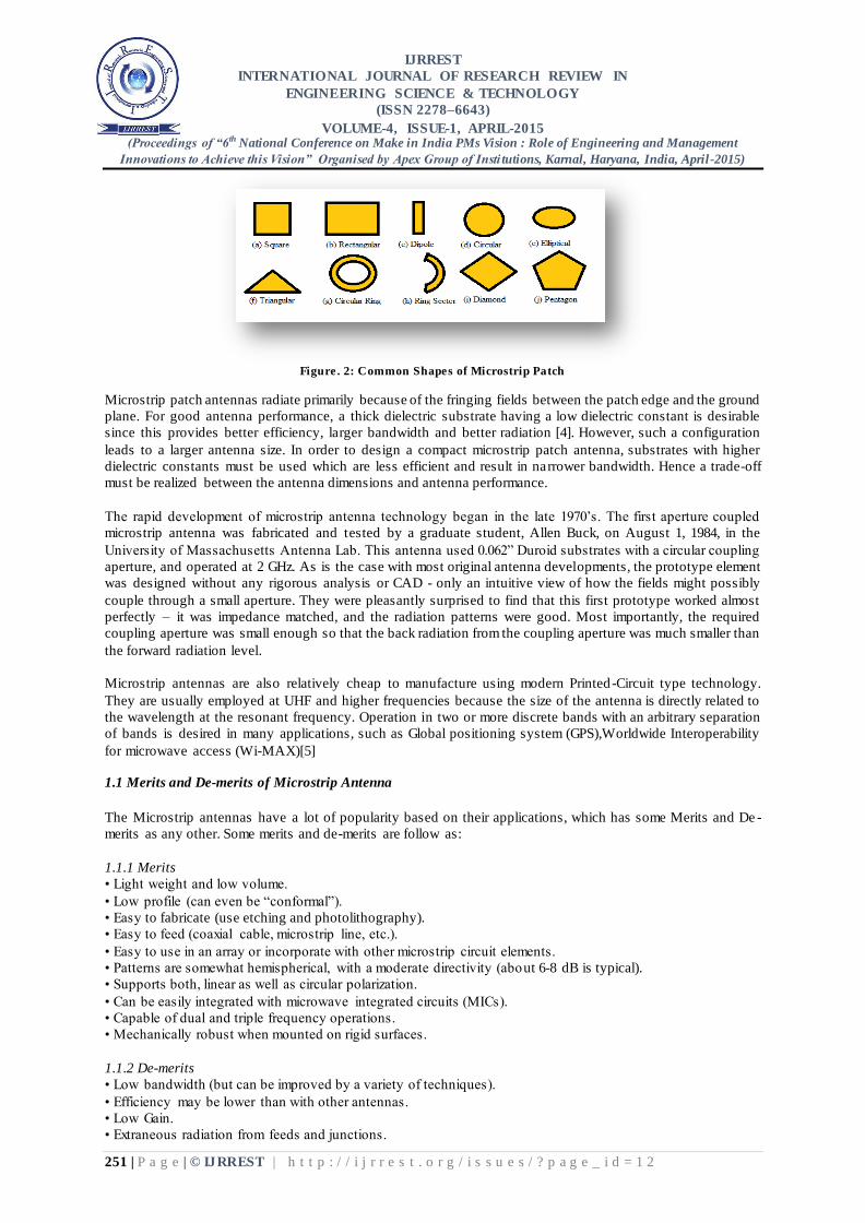
patch is generally square, rectangular, circular, triangular, and elliptical or some other common shape as shown
in Figure 2 Square, rectangle, dipole and circular are the most common because of ease of analysis and
fabrication, and their attractive radiation characteristics.
IJRREST
INTERNATIONAL JOURNAL OF RESEARCH REVIEW IN
ENGINEERING SCIENCE & TECHNOLOGY
(ISSN 2278–6643)
VOLUME-4, ISSUE-1, APRIL-2015 (Proceedings of “6th National Conference on Make in India PMs Vision : Role of Engineering and Management
Innovations to Achieve this Vision” Organised by Apex Group of Insti tutions, Karnal, Haryana, India, April-2015)
251 | P a g e | © IJRREST | h t t p : / / i j r r e s t . o r g / i s s u e s / ? p a g e _ i d = 1 2
Figure . 2: Common Shapes of Microstrip Patch
Microstrip patch antennas radiate primarily because of the fringing fields between the patch edge and the ground
plane. For good antenna performance, a thick dielectric substrate having a low dielectric constant is desirable
since this provides better efficiency, larger bandwidth and better radiation [4]. However, such a configuration
leads to a larger antenna size. In order to design a compact microstrip patch antenna, substrates with higher
dielectric constants must be used which are less efficient and result in narrower bandwidth. Hence a trade-off
must be realized between the antenna dimensions and antenna performance.
The rapid development of microstrip antenna technology began in the late 1970‟s. The first aperture coupled
microstrip antenna was fabricated and tested by a graduate student, Allen Buck, on August 1, 1984, in the
University of Massachusetts Antenna Lab. This antenna used 0.062” Duroid substrates with a circular coupling
aperture, and operated at 2 GHz. As is the case with most original antenna developments, the prototype element
was designed without any rigorous analysis or CAD - only an intuitive view of how the fields might possibly
couple through a small aperture. They were pleasantly surprised to find that this first prototype worked almost
perfectly – it was impedance matched, and the radiation patterns were good. Most importantly, the required
coupling aperture was small enough so that the back radiation from the coupling aperture was much smaller than
the forward radiation level.
Microstrip antennas are also relatively cheap to manufacture using modern Printed-Circuit type technology.
They are usually employed at UHF and higher frequencies because the size of the antenna is directly related to
the wavelength at the resonant frequency. Operation in two or more discrete bands with an arbitrary separation
of bands is desired in many applications, such as Global positioning system (GPS),Worldwide Interoperability
for microwave access (Wi-MAX)[5]
1.1 Merits and De-merits of Microstrip Antenna
The Microstrip antennas have a lot of popularity based on their applications, which has some Merits and De -
merits as any other. Some merits and de-merits are follow as:
1.1.1 Merits
• Light weight and low volume.
• Low profile (can even be “conformal”).
• Easy to fabricate (use etching and photolithography).
• Easy to feed (coaxial cable, microstrip line, etc.).
• Easy to use in an array or incorporate with other microstrip circuit elements.
• Patterns are somewhat hemispherical, with a moderate directivity (about 6-8 dB is typical).
• Supports both, linear as well as circular polarization.
• Can be easily integrated with microwave integrated circuits (MICs).
• Capable of dual and triple frequency operations.
• Mechanically robust when mounted on rigid surfaces.
1.1.2 De-merits
• Low bandwidth (but can be improved by a variety of techniques).
• Efficiency may be lower than with other antennas.
• Low Gain.
• Extraneous radiation from feeds and junctions.

IJRREST
INTERNATIONAL JOURNAL OF RESEARCH REVIEW IN
ENGINEERING SCIENCE & TECHNOLOGY
(ISSN 2278–6643)
VOLUME-4, ISSUE-1, APRIL-2015 (Proceedings of “6th National Conference on Make in India PMs Vision : Role of Engineering and Management
Innovations to Achieve this Vision” Organised by Apex Group of Insti tutions, Karnal, Haryana, India, April-2015)
252 | P a g e | © IJRREST | h t t p : / / i j r r e s t . o r g / i s s u e s / ? p a g e _ i d = 1 2
• Poor end fire radiator except tapered slot antennas.
• Low power handling capacity.
• Surface wave excitation.
1.2 Applications of MSAs
The applications are in the various fields such as in the medical applications, satellites and of course even in the
military systems just like in the rockets, aircrafts mis siles etc. the usage of the Microstrip antennas are spreading
widely in all the fields and areas and now they are booming in the commercial aspects due to their low cost of
the substrate material and the fabrication[6].
1.2.1 Mobile and satellite communication application
Microstrip patch antenna meets all requirements and various types of microstrip antennas have been designed
for use in mobile communication systems. In case of satellite communication circularly polarized radiation
patterns are required and can be realized using either square or circular patch with one or two feed points.
1.2.2Global Positioning System applications
Nowadays microstrip patch antennas with substrate having high permittivity sintered material are used for
global positioning system. These antennas are circularly polarized, very compact and quite expensive due to its
positioning. It is expected that millions of GPS receivers will be used by the general population for land
vehicles, aircraft and maritime vessels to find their position accurately.
1.2.3 Radio Frequency Identification (RFID)
RFID uses in different areas like mobile communication, logistics, manufacturing, transport ation and health
care. RFID system generally uses frequencies between 30 Hz and 5.8 GHz depending on its applications.
Basically RFID system is a tag or transponder and a transceiver or reader.
1.2.4 Worldwide Interoperability for Microwave Access (WiMAX)
The IEEE 802.16 standard is known as WiMAX. It can reach upto 30 mile radius theoretically and data rate 70
Mbps. MPA generates three resonant modes at 2.7, 3.3 and 5.3 GHz and can, therefore, be used in WiMAX
compliant communication equipment.
1.2.5 Radar Application
Radar can be used for detecting moving targets such as people and vehicles. It demands a low profile, light
weight antenna subsystem, the microstrip antennas are an ideal choice. The fabrication technology based on
photolithography enables the bulk production of microstrip antenna with repeatable performance at a lower cost
in a lesser time frame as compared to the conventional antennas.
1.2.6 Rectenna Application
Rectenna is a rectifying antenna, a special type of antenna that is used to directly convert microwave energy into
DC power. Rectenna is a combination of four subsystems i.e. Antenna, ore rectification filter, rectifier, post
rectification filter. In rectenna application, it is necessary to design antennas with very high directive
characteristics to meet the demands of long-distance links. Since the aim is to use the rectenna to transfer DC
power through wireless links for a long distance, this can only be accomplished by increasing the electrical size
of the antenna.
1.2.7 Telemedicine Application
In telemedicine application antenna is operating at 2.45 GHz. Wearable microstrip antenna is suitable for
Wireless Body Area Network (WBAN). The proposed antenna achieved a higher gain and front to back ratio
compared to the other antennas, in addition to the semi directional radiation pattern which is preferred over the
omni-directional pattern to overcome unnecessary radiation to the user's body and satisfies the requirement for
on-body and off-body applications. A antenna having gain of 6.7 dB and a F/B ratio of 11.7 dB and resonates at
2.45GHz is suitable for telemedicine applications.
1.2.8 Medicinal applications of patch
It is found that in the treatment of malignant tumors the microwave energy is said to be the most effective way
of inducing hyperthermia.

IJRREST
INTERNATIONAL JOURNAL OF RESEARCH REVIEW IN
ENGINEERING SCIENCE & TECHNOLOGY
(ISSN 2278–6643)
VOLUME-4, ISSUE-1, APRIL-2015 (Proceedings of “6th National Conference on Make in India PMs Vision : Role of Engineering and Management
Innovations to Achieve this Vision” Organised by Apex Group of Insti tutions, Karnal, Haryana, India, April-2015)
253 | P a g e | © IJRREST | h t t p : / / i j r r e s t . o r g / i s s u e s / ? p a g e _ i d = 1 2
1.3 Feed Techniques
There are many configurations that can be used to feed microstrip antennas. These feed techniques or methods
are being put as two different categories.[1-2]
Direct Methods:
Coaxial Probe Feed
Microstrip line Feed
Indirect Methods:
Electromagnetic Coupling
2.Aperture Coupling
3.Coplanar Waveguide Feed
Direct feed technique is the one where the power is being fed directly to radiating patch through the connecting
element i.e. through the Microstrip line.
Indirect feed technique is the one where an electromagnetic coupling is done to transfer the power between the
Microstrip line and the radiating patch.
There are few factors which lead or involve in the selection of a particular type of feed technique.
The first and the foremost factor is the efficient power transfer between the radiating structure and the
feed structure, i.e. the impedance that is matching between the two [2].
The minimization of the radiation and the effect of it‟s on the radiation patte rn is one of the most
important aspect for the evaluation of feed. Hence, microstrip patch antennas can be fed by a variety of
methods[1].
The four most popular feed techniques used are the microstrip line, coaxial probe (both contacting schemes),
aperture coupling and proximity coupling (both non-contacting schemes).
1.3.1 Microstrip Line Feed
A conducting strip is connected directly to the edge of the microst rip patch as shown in Figure 3. Direct feed
technique is the one where the power is being fed directly to radiating patch through the connecting element i.e.
through the Microstrip line. The conducting strip is smaller in width as compared to the patch and this kind of
feed arrangement has the advantage that the feed can be etched on the same substra te to provide a planar
structure. The purpose of the inset cut in the patch is to match the impedance of the feed line to the patch
without the need for any additional matching element. This is achieved by properly controlling the inset
position. Hence this is an easy feeding scheme, since it provides ease of fabrication and simplicity in modeling
as well as impedance matching. However as the thickness of the dielectric substrate being used, increases,
surface waves and spurious feed radiation also increases, which hampers the bandwidth of the antenna [1, 2].
The feed radiation also leads to undesired cross polarized radiation.
Figure . 3: Microstrip Line Feeding
Advantages:
Simple
Allows for planar feeding
Easy to obtain input match Disadvantages:
Significant line radiation for thicker substrates
For deep notches, pattern may show distortion

IJRREST
INTERNATIONAL JOURNAL OF RESEARCH REVIEW IN
ENGINEERING SCIENCE & TECHNOLOGY
(ISSN 2278–6643)
VOLUME-4, ISSUE-1, APRIL-2015 (Proceedings of “6th National Conference on Make in India PMs Vision : Role of Engineering and Management
Innovations to Achieve this Vision” Organised by Apex Group of Insti tutions, Karnal, Haryana, India, April-2015)
254 | P a g e | © IJRREST | h t t p : / / i j r r e s t . o r g / i s s u e s / ? p a g e _ i d = 1 2
1.3.2 Co-axial Feed
The Coaxial feed or probe feed is a very common technique used for feeding Microstrip patch antennas. As seen
from Figure 4, the inner conductor of the coaxial connector extends through the dielectric and is soldered to the
radiating patch, while the outer conductor is connected to the ground plane.
Figure . 4: Coaxial feeding
Also, for thicker substrates, the increased probe length makes the input impedance more inductive, leading to
matching problems. It is seen above that for a thick dielectric substrate, which provides broad bandwidth, the
microstrip line feed and the coaxial feed suffer from numerous disadvantages. The indirect feed techniques
solve these issues.
Advantages:
Simple
Easy to obtain input match
Disadvantages:
Difficult to obtain input match for thicker substrates,
due to probe inductance.
Significant probe radiation for thicker substrates
It provides narrow bandwidth and is difficult to model since a hole has to be drilled in the substrate and
the connector protrudes outside the ground plane, thus not making it completely planar for thick
substrates (h > 0.02λo).
1.3.3 Aperture Coupled Feed
The radiating patch and the microstrip feed line are separated by the gro und plane as shown in Figure 5.
Coupling between the patch and the feed line is made through a slot or an aperture in the ground plane.
Figure . 5: Aperture Coupled Feed
The coupling aperture is usually centered under the patch, leading to lower cross polarization due to symmetry
of the configuration. The amount of coupling from the feed line to the patch is determined by the shape, size and
location of the aperture. Since the ground plane separates the patch and the feed line, spurious radiation is
minimized. Generally, a high dielectric material is used for bottom substrate and a thick, low dielectric consta nt
material is used for the top substrate to optimize radiation from the patch.

IJRREST
INTERNATIONAL JOURNAL OF RESEARCH REVIEW IN
ENGINEERING SCIENCE & TECHNOLOGY
(ISSN 2278–6643)
VOLUME-4, ISSUE-1, APRIL-2015 (Proceedings of “6th National Conference on Make in India PMs Vision : Role of Engineering and Management
Innovations to Achieve this Vision” Organised by Apex Group of Insti tutions, Karnal, Haryana, India, April-2015)
255 | P a g e | © IJRREST | h t t p : / / i j r r e s t . o r g / i s s u e s / ? p a g e _ i d = 1 2
Advantages:
Allows for planar feeding
Feed radiation is isolated from patch radiation
Higher bandwidth, since probe inductance problem restriction is eliminated and a double-resonance can
be created.
Allows for use of different substrates to optimize antenna and feed-circuit performance.
Disadvantages:
Requires multilayer fabrication
Alignment is important for input match
1.3.4 Proximity Coupled Feed
It is also called as the electromagnetic coupling scheme. As shown in Figure 6, two dielectric substrates are used
such that the feed line is between the two substrates and the radiating patch is on top of the upper substrate. This
scheme also provides choices between two different dielectric media, one for the patch and one for the feed line
to optimize the individual performances. Matching can be achieved by controlling the length of the feed line and
the width to line ratio of the patch
Figure. 6: Proximity Coupled Feed
Advantages:
Allows for planar feeding
Less line radiation compared
It eliminates spurious feed radiation and provides very high bandwidth (as high as 13%), due to overall
increase in the thickness of the microstrip patch antenn to microstrip feed.
Disadvantages:
Requires multilayer fabrication
Alignment is important for input match
1.3.5 Coplanar Waveguide Feed
The coplanar waveguide feed shown in Figure 7has also been used to excite the MSA [2]. In this method, the
coplanar waveguide is etched on the ground plane of the MSA. The line is excited by a coaxial feed and is
terminated by a slot, whose length is chosen to be between 0.25 and 0.29 of the slot wavelength. The main
disadvantage of this method is the high radiation from the rather longer slot, leading to the poor front-to back
ratio. The front-to-back ratio is improved by reducing the slot dimension and modifying its shape in the form of
a loop.
Figure . 7: CPW Line Feed
1.4 Methods of Analysis
The preferred models for the analysis of microstrip patch antennas are the transmission line model, cavity
model, and full wave model (which include primarily integral equations/Moment Method). The transmission
line model is the simplest of all and it gives good physical insight [7].

IJRREST
INTERNATIONAL JOURNAL OF RESEARCH REVIEW IN
ENGINEERING SCIENCE & TECHNOLOGY
(ISSN 2278–6643)
VOLUME-4, ISSUE-1, APRIL-2015 (Proceedings of “6th National Conference on Make in India PMs Vision : Role of Engineering and Management
Innovations to Achieve this Vision” Organised by Apex Group of Insti tutions, Karnal, Haryana, India, April-2015)
256 | P a g e | © IJRREST | h t t p : / / i j r r e s t . o r g / i s s u e s / ? p a g e _ i d = 1 2
1.4.1 Transmission Line Model
This model represents the microstrip antenna by two slots of width W and height h, separated by a transmission
line of length L. The microstrip is essentially a nonhomogeneous line of two dielect rics, typically the substrate
and air.
Figure . 8: Electric fie ld lines between patch and ground plane.
Hence, as seen from Figure 8 most of the electric field lines reside in the substrate and parts of some lines in air.
As a result, this transmission line cannot support pure transverse electromagnetic (TEM) mode of transmission,
since the phase velocities would be different in the air and the substrate. Instead, the dominant mode of
propagation would be the quasi TEM mode. Hence, an effect ive dielectric constant (εre) must be obtained in
order to account for the fringing and the wave propagation in the line. The value of ε re is slightly less than εr
because the fringing fields around the periphery of the patch are not confined in the dielec tric substrate but are
also spread in the air as shown in Figure above. The expression for εre is
Where εre = Effective dielectric constant
εr = Dielectric constant of substrate
h = Height of dielectric substrate
W =Width of the patch
In order to operate in the fundamental TM10 mode, the length of the patch must be slightly less than λ/2 where λ
is the wavelength in the dielectric medium and is equal to λo/√εreff where λo is the free space wavelength. The
TM10 mode implies that the field varies one λ/2 cycle along the length, and there is no variation along the width
of the patch [2]. In the Figure 9 shown below, the microstrip patch antenna is represented by two slots, separated
by a transmission line of length L and open circuited at both the ends. Along the width of the patch, the voltage
is maximum and current is minimum due to the open ends. The fields at the edges can be resolved into normal
and tangential components with respect to the ground plane.
Figure . 9: Top view of microstrip antenna
Figure . 10: Side view of patch antenna

IJRREST
INTERNATIONAL JOURNAL OF RESEARCH REVIEW IN
ENGINEERING SCIENCE & TECHNOLOGY
(ISSN 2278–6643)
VOLUME-4, ISSUE-1, APRIL-2015 (Proceedings of “6th National Conference on Make in India PMs Vision : Role of Engineering and Management
Innovations to Achieve this Vision” Organised by Apex Group of Insti tutions, Karnal, Haryana, India, April-2015)
257 | P a g e | © IJRREST | h t t p : / / i j r r e s t . o r g / i s s u e s / ? p a g e _ i d = 1 2
It is seen from Figure 10 that the normal components of the electric field at the two edges along the width are in
opposite directions and thus out of phase since the patch is λ/2 long and hence they cancel each other in the
broadside direction.
The tangential components which are in phase, means that the resulting fields combine to give maximum
radiated field normal to the surface of the structure. Hence the edges along the width can be represented as two
radiating slots, which are λ/2 apart and excited in phase and radiating in the half space above the ground plane.
The fringing fields along the width can be modeled as radiating slots and electrically the patch of the microstrip
antenna looks greater than its physical dimensions. The dimensions of the patch along its length have now been
extended on each end by a distance ΔL, which is
The effective length of the patch Leff now becomes
Leff =L+2Δ
The width W is
1.4.2 Cavity Model
Although the transmission line model is easy to use, it has some inherent disadvantages. Specifically, it is useful
for patches of rectangular design and it ignores field variations along the radiating edges. These disadvantages
can be overcome by using the cavity model [2].
In the cavity model, the region between the patch and the ground plane is treated as a cavity that is surrounded
by magnetic walls around the periphery and by electric walls from the top and bottom sides. Since thin
substrates are used, the field inside the cavity is uniform along the thickness of the substrate. The fields
underneath the patch for regular shapes such as rectangular, circular, triangular, and sectoral shapes can be
expressed as a summation of the various resonant modes of the two-dimensional resonator.
The fringing fields around the periphery are taken care of by extending the patch boundary outward so that the
effective dimensions are larger than the physical dimensions of the patch. The effect of the radiation fro m the
antenna and the conductor loss are accounted for by adding these losses to the loss tangent of the dielectric
substrate. The far field and radiated power are computed from the equivalent magnetic current around the
periphery.
An alternate way of incorporating the radiation effect in the cavity model is by introducing an impedance
boundary condition at the walls of the cavity. The fringing fields and the radiated power are not included inside
the cavity but are localized at the edges of the cavity.
2. ANTENNA PARAMETERS
An antenna is a transformer between a transmission line and free space. To describe an antenna, we must
characterize its properties as a transmission line load (input impedance) and the distribution of the
electromagnetic energy that it radiates into space (radiation pattern). There are a number of key parameters and
concepts that we can use to describe antenna properties.Let us discuss these parameters in detail [1,2].
2.1 Return loss
This is the best and convenient method to calculate the input and output of the signal sources. It can be said that
when the load is mismatched the whole power is not delivered to the load there is a return of the power and that
is called loss, and this loss that is returned is called the „Return loss‟.
This Return Loss is determined in dB as follows:
RL = -20log |Г| (dB)
|Г| is the reflection coefficient
IJRREST
INTERNATIONAL JOURNAL OF RESEARCH REVIEW IN
ENGINEERING SCIENCE & TECHNOLOGY
(ISSN 2278–6643)
VOLUME-4, ISSUE-1, APRIL-2015 (Proceedings of “6th National Conference on Make in India PMs Vision : Role of Engineering and Management
Innovations to Achieve this Vision” Organised by Apex Group of Insti tutions, Karnal, Haryana, India, April-2015)
258 | P a g e | © IJRREST | h t t p : / / i j r r e s t . o r g / i s s u e s / ? p a g e _ i d = 1 2
VO
+ The incident voltage
VO-
The reflected voltage
ZL and ZO the load and characteristic impedances.
To have a perfect matching between the antenna and the transmitter, Г=0 and RL = ∞, this indicates that there is
no power that is returned or reflected but when Г=0 and RL = 0dB, this indicated that the power that is se nt is
all reflected back.
2.2 Bandwidth
Bandwidth can be said as the frequencies on both the sides of the centre frequency in which the characteristics
of antenna such as the input impedance, polarization, beam width, radiation pattern etc are almost close to that
of this value. As the definition goes “the range of suitable frequencies within which the performance of the
antenna, w.r.t some characteristic, conforms to a specific standard”.
The bandwidth is the ratio of the upper and lower frequencies of an operation. The bandwidth can be obtained
as:
BW = 100 × (FH − FL)/FC
Where, FH is the highest frequency in the band, FL is the lowest frequency in the band, and FC is the center
frequency in the band.
2.3 Gain and Directivity
The gain of the antenna is the quantity which describes the performance of the antenna or the capability to
concentrate energy through a direction to give a better picture of the radiation performance. This is expressed in dB, in a simple way we can say that this refers to the direction of the maximum radiation.
The expression for the maximum gain of an antenna is as follows:
G = η x D
η – The efficiency of the antenna
D – Directivity
In order to receive or transmit the power it can be chosen to maximize the radiation pattern of the response of
the antenna in a particular direction.
The directivity of an antenna can be defined as the ratio of radiation intensity in a given direction from the
antenna to the radiation intensity averaged in all the directions. And the gain can be known as the ratio between
the amounts of energy propagated in these directions to the energy that would be propagated if there is an Omni-
directional antenna. The directivity of the antenna depends on the shape of the radiation pattern. The
measurement is done taking a reference of isotropic point source from the response. The quantitative measure of
this response is known as the directive gain for the antenna on a given direction.
2.4 Radiation Pattern
The radiation or antenna pattern describes the relative strength of the radiated field in various directions from
the antenna, at a constant distance. The radiation pattern describes the receiving properties of the antenna. The
radiation pattern is three-dimensional, but usually the measured radiation patterns are a two-dimensional slice of
the three-dimensional pattern, in the horizontal or vertical planes. These pattern measurements are presented in
either a rectangular or a polar format.
The radiation pattern of a generic dimensional antenna can be seen below, which consist of side lobe, black
lobes, and are undesirable as they represent the energy that is wasted for transmitting antennas and noise sources
at the receiving end.

IJRREST
INTERNATIONAL JOURNAL OF RESEARCH REVIEW IN
ENGINEERING SCIENCE & TECHNOLOGY
(ISSN 2278–6643)
VOLUME-4, ISSUE-1, APRIL-2015 (Proceedings of “6th National Conference on Make in India PMs Vision : Role of Engineering and Management
Innovations to Achieve this Vision” Organised by Apex Group of Insti tutions, Karnal, Haryana, India, April-2015)
259 | P a g e | © IJRREST | h t t p : / / i j r r e s t . o r g / i s s u e s / ? p a g e _ i d = 1 2
Figure . 11: Radiation Pattern of a generic dimensional antenna
There are two kinds of radiation pattern: absolute and relative. Absolute radiation patterns are presented in
absolute units of field strength or power. Relative radiation patterns are referenced in relative units of field
strength or power. Most radiation pattern measurements are relative to the isotropic antenna, and then the gain
transfer method is then used to establish the absolute gain of the antenna.
2.5 Polarization
The polarization of the electric field vector of the radiated wave or from source Vs time the observation of the
orientation of the electric fields does also refer to the polarization. It is defined as “the property of an
electromagnetic wave describing the time varying direction and relative magnitude of the electric filed vector”
The direction or position of the electric field w.r.t the ground gives the wave polarization. The common types of
the polarization are circular and linear the former includes horizontal and vertical and the latter includes right
hand polarization and left hand polarization.
Figure . 12: A linearly polarized wave
It is said to be linearly polarized when the path of the electric field vector is back and forth along the line. It can
be noted that the circular polarization has the electric field vector‟s length constant but rotates in a circular path.
2.6 Reflection Coefficient |Г| and Character Impedance (Z0)
There is a reflection that occurs in the transmission line when we take the h igher frequencies in to consideration.
There is a resistance that is associated with each transmission line which comes with the construction of the
transmission line. This is called as character impedance (Z0). The standard value of this impedance is 50ohm.
Always the every transmission line is being terminated with an arbitrary load ZL and this is not equivalent to the
impedance i.e. Z0. Here occurs the reflected wave.
The degree of impedance mismatch is represented by the reflection coefficient [1] at that load and is given by:
We can observe here that the reflection coefficient for the shorted load ZL=0, there is a match in the load ZL=Z0
and an open load ZL = ∞ are -1, 0, +1.

IJRREST
INTERNATIONAL JOURNAL OF RESEARCH REVIEW IN
ENGINEERING SCIENCE & TECHNOLOGY
(ISSN 2278–6643)
VOLUME-4, ISSUE-1, APRIL-2015 (Proceedings of “6th National Conference on Make in India PMs Vision : Role of Engineering and Management
Innovations to Achieve this Vision” Organised by Apex Group of Insti tutions, Karnal, Haryana, India, April-2015)
260 | P a g e | © IJRREST | h t t p : / / i j r r e s t . o r g / i s s u e s / ? p a g e _ i d = 1 2
Hence, we can say that the reflection coefficient ranges from 0 to +1.
2.7 Voltage Standing Wave Ratio (VSWR)
There should be a maximum power transfer between the transmitter and the ant enna for the antenna to perform
efficiently. This happens only when the impedance Z in is matched to the transmitter impedance, Zs.
In the process of achieving this particular configuration for an antenna to perform efficiently there is always a
reflection of the power which leads to the standing waves, which is characterized by the Voltag e Standing Wave
Ratio (VSWR).
This is given by :
As the reflection coefficient ranges from 0 to 1, the VSWR ranges from 1 to ∞
3. TECHNIQUES USED TO IMPROVE THE RESONANCE BANDWIDTH AND REDUCE THE SIZE
OF PATCH ANTENNA
Microstrip antennas are investigated vastly due to their properties, such as low profile, low cost, conformability
and ease of integration with active devices. The size of antenna and bandwidth is extremely important for most
wireless communication systems. Various design techniques of microstrip antenna grow rapidly especially to
improve resonant bandwidth such as use a L-shaped and U-shaped coplanar feed-line in the slot of the square
patch [8,9,11], optimizing rectangular patch by combination of genetic algorithm and finite element softwa re,
use L-probe feeding technique on inverted novel patch with air-filled dielectric, and slotted patch , also circular
ring micro strip antenna was proposed to enhance the bandwidth. However, the bandwidth and the size of an
antenna are generally conflicting properties, that is, improvement of one of the characteristics normally results
in degradation of the other.
Intended application on mobile network nodes such as portable laptop platforms, compactness was a key issue
that was considered in the designs [10]. But it is desired that the reduced size antenna have equivalent operation
in comparison with ordinary developed antennas. There are limits to how small an antenna can be, however the
most important of them are bandwidth and gain. Fortunately a lot o f communication systems don‟t require large
bandwidths; therefore, it is not an important problem. Many techniques have been used to reduce the size of
antenna, such as using dielectric substrates with high permittivity, applying resistive or reactive load ing,
increasing the electrical length of antenna by optimizing its shape , Utilization of strategically positioned
notches on the patch antenna . Various shapes of slots and slits have been embedded on patch antennas to reduce
their size. Such slot loading causes the meandering of the surface current, thus effectively increasing the surface
current path and the electrical length of the element that leads to reduction of the patch size for a given resonant
frequency. Simultaneous etching out of a symmetrical array of slots and the excitation of two orthogonal modes
can lead to an antenna with reduced size operating in dual-polarization mode.
Some new technologies to enhance the whole quality of system such as:[11]
Low-temperature co-fire ceramic technology (LTCC),
Low-temperature co-fire ferrite (LTCF)
Photonic band gap (PBG),
Defected ground structure(DGS),
Ground plane aperture(GPA)
Substrate integrate wave-guide (SIW) and so on.
Consequently, there has been an increasing interest in microwave and millimetre-wave applications of PBG.
Similarly, there is another new ground plane aperture (GPA) technique which simply incorporates the microstrip
line with a centered slot at the ground plane, and the use of GPA has attractive applications in 3 dB edge c oupler
for tight coupling and band pass filters for spurious band suppression and enhanced coupling. PBG is a periodic
structure which has been known as providing rejection of certain frequency band. However, it is difficult to use
a PBG structure for the design of the microwave or millimeter-wave components due to the difficulties of
modeling. There are so many design parameters that effect on the band gap property, such as the number of
lattice, lattice shapes, lattice spacing and relative volume fraction. Another problem is caused by the radiation

IJRREST
INTERNATIONAL JOURNAL OF RESEARCH REVIEW IN
ENGINEERING SCIENCE & TECHNOLOGY
(ISSN 2278–6643)
VOLUME-4, ISSUE-1, APRIL-2015 (Proceedings of “6th National Conference on Make in India PMs Vision : Role of Engineering and Management
Innovations to Achieve this Vision” Organised by Apex Group of Insti tutions, Karnal, Haryana, India, April-2015)
261 | P a g e | © IJRREST | h t t p : / / i j r r e s t . o r g / i s s u e s / ? p a g e _ i d = 1 2
from the periodic etched defects. Furthermore, with the introduction of a GPA below the strip, the line
properties could be changed significantly as the characteristic impedance varies with the width of the GPA.
Usually the GPA is considered as the basis of equivalent J-inverter circuit theory and its filtering behavior has
been characterized by a closed form equation. As a technique to improve circuit performance, there is more
investigations on the applications than the essence of GPA. In order to alleviate these problems Park et al.
proposed DGS which is designed by connecting two square PBG cells with a thin slot. DGS which bases on
GPA focuses not only on its application but also on its own characteristics. DGS adds an extra degree of
freedom in microwave circuit design and opens the door to a wide range of application. In the following years, a
great lot of novel DGSs were proposed and they had become one of the most interesting areas of research owing
to their extensive applicability in microwave circuits. The parameters of equivalent circuit‟s models of DGSs
were also researched and utilized to design planar circuit easily. Many passive and active microwave and
millimeter devices have been developed to suppress the harmonics and realize the compact physical dimensions
of circuits for the design flow of circuits with DGS comparatively simple.
4. CONCLUS ION
In this paper the basics of microstrip patch antenna(MPA), various feeding techniques, design model and
antenna parameters is studied . MPA have various number of advantages like Light weight and low volume,
Easy to fabricate. But MPA have narrow bandwidth so to enhance bandwidth various techniques are engaged .
Many techniques have been used to reduce the size and increase the bandwidth of antenna is discussed , such as
using dielectric substrates with high permittivity, applying resistive or reactive loading, increasing the electrical
length of antenna by optimizing its shape , Utilization of strategically positioned notches on the patch antenna .
5. REFERENCES
[1] C. A. Balanis, “Antenna Theory, Analysis and Design,” John Wiley & Sons, New York, 1997.
[2] Girish Kumar, K.P. Ray, “Broadband Microstrip Antennas” Artech House, 2003.
[3] www.wikipidea.com [4] Islam, F., Ali, M. , Majlis, B.Y. , Misran, N, “Design, simulation and fabrication of a microstrip patch antenna for
dual band application,” International Conference on Electrical and Computer Engineering, pp. 799 – 802, Dec. 2008.
[5] J. Chen, Z.-B. Weng, Y.-C. Jiao, and F.-S. Zhang, “Lowpass filter design of Hilbert curve ring defected ground,”
Progress in Electromagnetics Research, PIER 70, pp. 269–280, 2007.
[6] U. Chakraborty, “A Compact microstrip patch antenna for wireless communication,” Progress In Electromagnetics Research C, Vol. 18, pp. 211-220, 2011.
[7] Sudhir Bhaskar & Sachin Kumar Gupta, “Bandwidth Improvement of Microstrip Patch Antenna Using H-Shaped
Patch,” International Journal of Engineering Research and Applications (IJERA) ISSN: 2248-9622, Vol. 2, Issue 1,
pp. 334-33, 2012.
[8] A. Kordzadeh and F. Hojat Kashani, “A New reduced size Microstrip patch antenna with fractal shaped defects,” Progress In Electromagnetics Research B, Vol. 11, pp. 29–37, 2009.
[9] Ashwini K. Arya, M.V. Kartikeyan, A.Patnaik, “Defected Ground Structure in the perspective of Microstrip Antennas:
A Review,” IJERA , 2010.
[10] Keyoor Gosalia and Gianluca Lazzi,“Reduced Size, Dual-Polarized Microstrip Patch Antenna for Wireless
Communications,” IEEE Transactions on antennas and propagation, Vol. 51, No. 9, Sept. 2003. [11] L. H. Weng, Y. C. Guo, X. W. Shi, and X. Q. Chen “An Overview on defected ground structure,” Progress In
Electromagnetics Research B, Vol. 7, pp. 173–189, 2008.
[12] Rajeshwar Lal Dua, Himanshu Singh, Neha Gambhir, “2.45 GHz Microstrip antenna with Defected Ground
Structure for Bluetooth,” International Journal of Soft Computing and Engineering (IJSCE) ISSN: 2231-2307,
Volume-1, Issue-6, January 2012. [13] Susanta Kumar PARUI, Santanu DAS, “A New Defected Ground Structure for Different Microstrip Circuit
Applications,” Radioengineering, Vol. 16, No. 1, April 2007.
[14] Ayman A. R. Saad, Elsayed E. M. Khaled, and Deena A. Salem, “Wideband Slotted Planar Antenna with Defected
Ground Structure,” PIERS Proceedings, Suzhou, China, September pp.12-16, 2011.