Interconnect Area - University of Texas at Austinusers.ece.utexas.edu/~roth/book/CH6_Slides.pdfCLK...
43
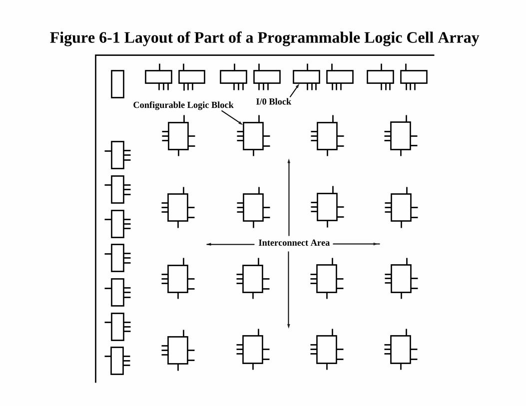
I/0 Block Configurable Logic Block Interconnect Area Figure 6-1 Layout of Part of a Programmable Logic Cell Array
Transcript of Interconnect Area - University of Texas at Austinusers.ece.utexas.edu/~roth/book/CH6_Slides.pdfCLK...
I/0 BlockConfigurable Logic Block
Interconnect Area
Figure 6-1 Layout of Part of a Programmable Logic Cell Array
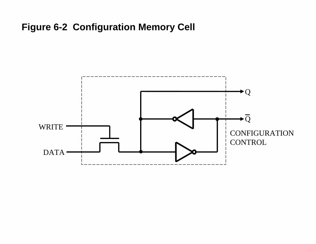
Figure 6-2 Configuration Memory Cell
WRITE
DATA
Q
Q
CONFIGURATIONCONTROL

M M
EDCB
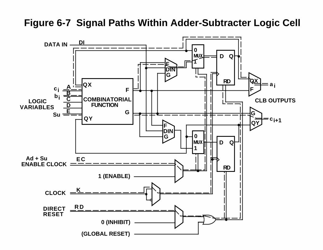
DATA IN DI
A
CLB OUTPUTS
X
0 (INHIBIT)
(GLOBAL RESET)
LOGICVARIABLES
QX
QYG
FCOMBINATORIAL
FUNCTION
FDING
1MUX0
RD
D Q
RD
D Q
DIRECTRESET
CLOCK
ENABLE CLOCK EC
K
RD
Y
1 (ENABLE)
Figure 6-3 Xilinx 3000 Series Logic Cell
M M
FDING
1MUX0
M
M
M
M
QXF
M
GQY
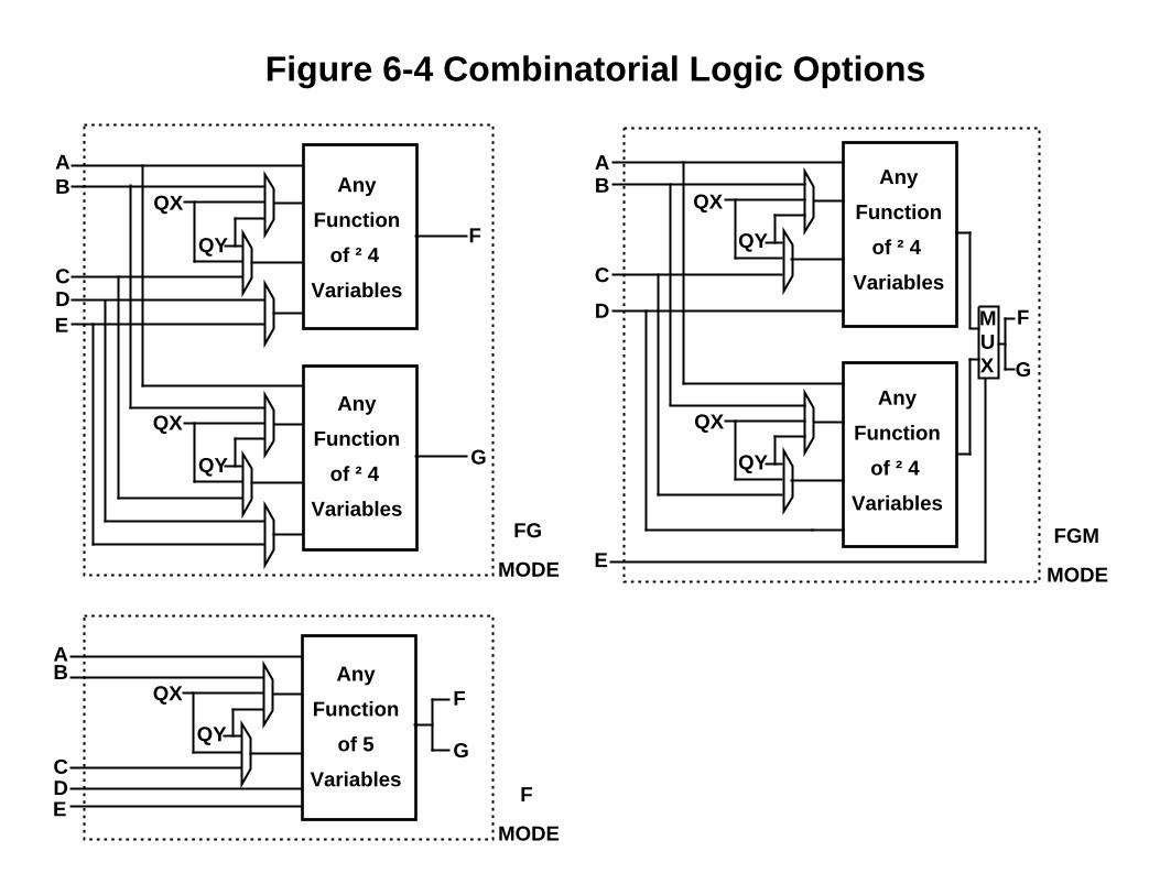
Any
Function
of ² 4
Variables
QX
QY F
AB
C
ED
QX
QY G
Any
Function
of 5
Variables
F
G
QX
QY
AB
C
ED
FG
MODE
F
MODE
Any
Function
of ² 4
Variables
QX
QY
QX
QY
AB
C
E
D MUX
F
G
FGM
MODE
Any
Function
of ² 4
Variables
Any
Function
of ² 4
Variables
Figure 6-4 Combinatorial Logic Options

Figure 6-5 Flip-flops with Clock Enable
Q+ = EC D1 + EC' Q
D Q
Reset
CEFFCLK
D1EC1
MUX0
RD
D QD1
ECCLK
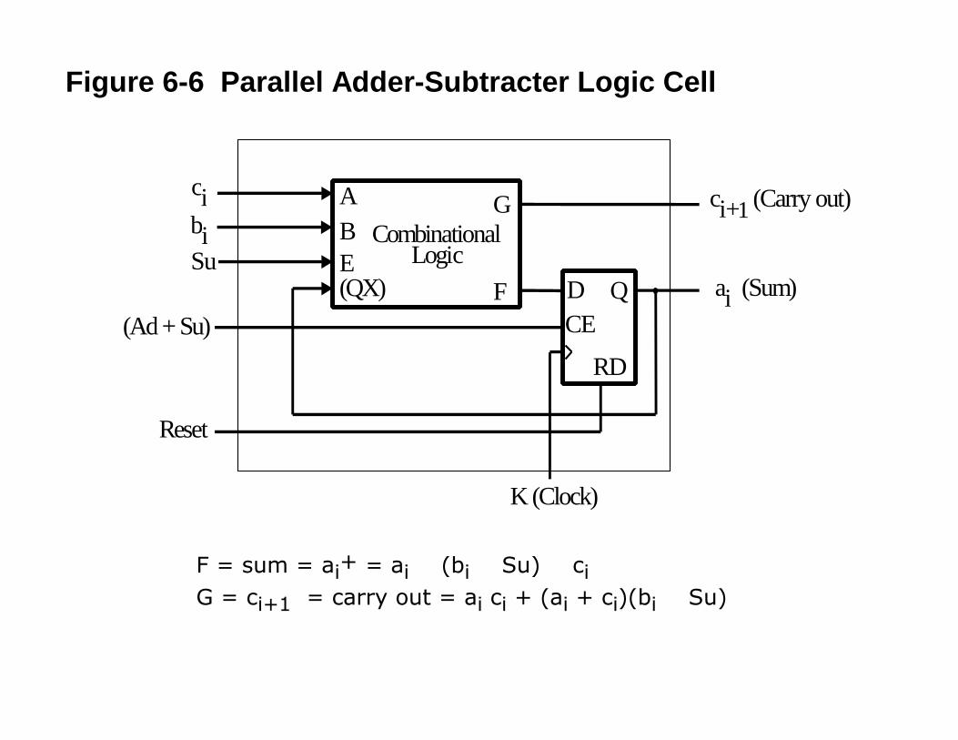
Figure 6-6 Parallel Adder-Subtracter Logic Cell
F = sum = ai+ = ai ⊕ (bi ⊕ Su) ⊕ ciG = ci+1 = carry out = ai ci + (ai + ci)(bi ⊕ Su)
BbiESu
F D Q
ACombinational
Logic
G
RD
Reset
ci+1 (Carry out)
ai (Sum)
K (Clock)
ci
(Ad + Su) CE(QX)
B
FDING
G
QY
F
EDCB
DATA IN DI
A
CLB OUTPUTS
0 (INHIBIT)
(GLOBAL RESET)
LOGICVARIABLES
QX
QYG
F
COMBINATORIALFUNCTION
1MUX0
RD
D Q
1MUX0
RD
D Q
DIRECTRESET
CLOCK
ENABLE CLOCKE C
K
R D
1 (ENABLE)
c i
Ad + Su
c i+1
b i
Su
a i
FDING
QX
Figure 6-7 Signal Paths Within Adder-Subtracter Logic Cell

OUTINVERT
3-STATEINVERT
OUTPUTSELECT
SLEWRATE
PASSIVEPULL UP
I/OPAD
TTL orCMOSINPUT
THRESHOLD
(GLOBAL RESET)
CK1
CK2
CK IK
I
QDIRECT IN
REGISTERED IN
T
O
3-STATE
OUT
(OUTPUT ENABLE)
Vcc
OUTPUTBUFFER
PROGRAMCONTROLLEDMULTIPLEXER = PROGRAMMABLE INTERCONNECTION POINT or PIP
D Q
R
FLIPFLOP
DQ
R
PROGRAM-CONTROLLED MEMORY CELLS
FLIPFLOP
orLATCH
Figure 6-8 Xilinx 3000 Series I/O Block

CLB CLB CLB
CLB CLBCLB
SwitchMatrix
SwitchMatrix
CLB
SwitchMatrix
CLB CLB
CLB
CLB CLB CLB
CLBCLB
SwitchMatrix
SwitchMatrix
SwitchMatrix
Figure 6-9General-purposeInterconnects
Figure 6-10Direct InterconnectsBetween Adjacent CLBs
CLB CLB
CLBCLB
SwitchMatrix
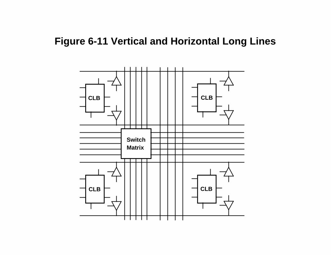
Figure 6-11 Vertical and Horizontal Long Lines
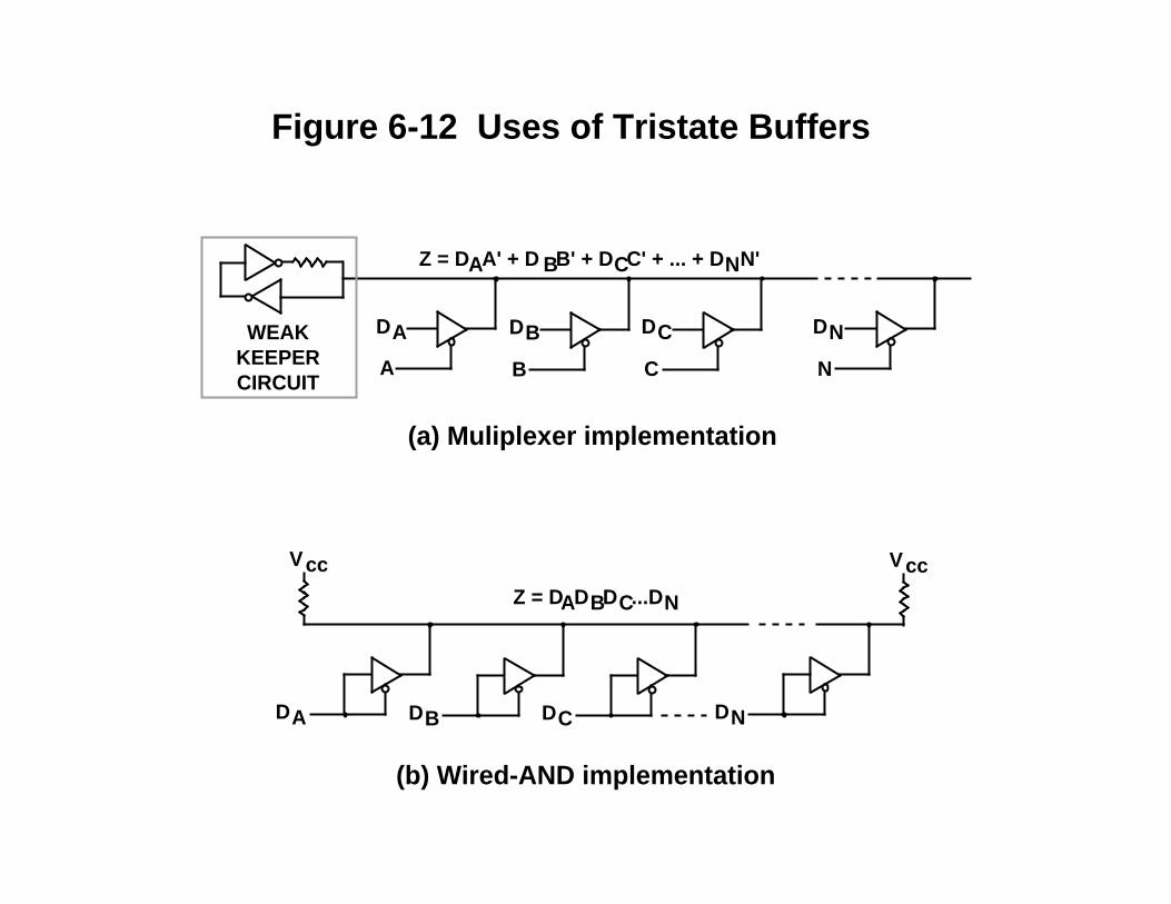
DA DB DC DN
Z = DAA' + D BB' + DCC' + ... + DNN'
WEAKKEEPERCIRCUIT
A B C N
Vcc Vcc
DA DB DC DN
Z = DADBDC...DN
Figure 6-12 Uses of Tristate Buffers
(a) Muliplexer implementation
(b) Wired-AND implementation

D Q
AlternateClock Buffer
XTAL2(IN)
XTAL1
R1
R2
C1 C2Y1
Figure 6-13 Crystal Oscillator
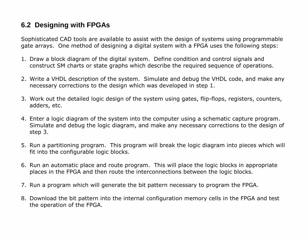
6.2 Designing with FPGAs
Sophisticated CAD tools are available to assist with the design of systems using programmablegate arrays. One method of designing a digital system with a FPGA uses the following steps:
1. Draw a block diagram of the digital system. Define condition and control signals andconstruct SM charts or state graphs which describe the required sequence of operations.
2. Write a VHDL description of the system. Simulate and debug the VHDL code, and make anynecessary corrections to the design which was developed in step 1.
3. Work out the detailed logic design of the system using gates, flip-flops, registers, counters,adders, etc.
4. Enter a logic diagram of the system into the computer using a schematic capture program.Simulate and debug the logic diagram, and make any necessary corrections to the design ofstep 3.
5. Run a partitioning program. This program will break the logic diagram into pieces which willfit into the configurable logic blocks.
6. Run an automatic place and route program. This will place the logic blocks in appropriateplaces in the FPGA and then route the interconnections between the logic blocks.
7. Run a program which will generate the bit pattern necessary to program the FPGA.
8. Download the bit pattern into the internal configuration memory cells in the FPGA and testthe operation of the FPGA.

Figure 6-14 EPROM Connection for LCA Initialization
FPGA
EPROM(contains
configurationdata)
Address
Data

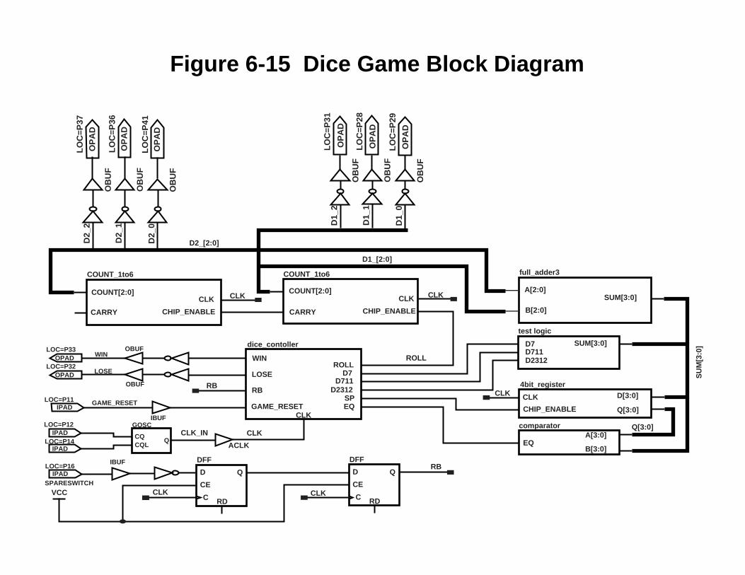
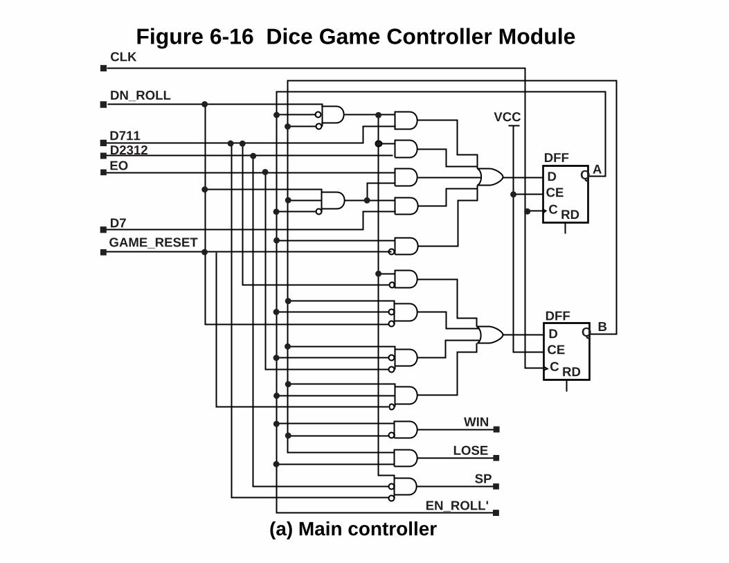
From Page 213Dice Game Controller Equations (From SM Chart of Figure 5-32)
State Assignment:T0: AB = 00, T1: AB = 01, T2: AB = 10, T3: AB = 11
A+ = A'B' Dn_roll D711 + A'B' Dn_roll D2312 + A'B Dn_roll Eq+ A'B Dn_roll D7 + A Reset'
B+ = A'B' Dn_roll D711' + A'B Dn_roll' + A'B Eq' + A B Reset'
Win = A B' Lose = A B En_roll = A'
Sp = A'B' Dn_roll D711' D2312'
Q+ = Q' En_roll Rb + Q Rb Roll = Q Rb Dn_roll = Q Rb'
CLKCE
D
DFF
Q
RDC CLKCE
D
DFF
Q
RDC
IPADSPARESWITCH
VCC
LOC=P16IBUF
IPADLOC=P14
LOC=P12IPAD CQ
CQLQ
GOSCCLK_IN
ACLK
CLK
CLKGAME_RESET
RB
LOSE
WINROLL
D7D711
D2312SPEQ
dice_contoller
ROLL
RB
RB
GAME_RESET
OPADLOC=P32
LOC=P33WIN
LOSE
OBUF
OBUFOPAD
IPADLOC=P11
IBUFcomparator
EQA[3:0]
B[3:0]
Q[3:0]
D[3:0]
Q[3:0]
4bit_register
CLK
CHIP_ENABLE
CLK
D7D711D2312
SUM[3:0]
test logic
A[2:0]
B[2:0]
SUM[3:0]
full_adder3
CLK
SU
M[3
:0]
COUNT_1to6
COUNT[2:0]
CARRY
CLK
CHIP_ENABLE
CLKCOUNT[2:0]
COUNT_1to6
CHIP_ENABLECARRY
CLK
D2_[2:0]
D1_[2:0]
LO
C=P
37O
PA
DD
2_2
OB
UF
LO
C=P
36O
PA
DD
2_1
OB
UF
LO
C=P
41O
PA
DD
2_0
OB
UF
LO
C=P
31
OP
AD
D1_
2
OB
UF
LO
C=P
28
OP
AD
D1_
1
OB
UF
LO
C=P
29
OP
AD
D1_
0
OB
UF
Figure 6-15 Dice Game Block Diagram
CLK
DN_ROLL
D711D2312EO
D7
GAME_RESET
VCC
DFFDCEC RD
Q A
DFFDCEC RD
Q B
WIN
LOSE
SP
EN_ROLL'
Figure 6-16 Dice Game Controller Module
(a) Main controller

DFF
D
CE
CRD
Q
CLKVCC
EN_ROLL'
RB
ROLL_NEXT
ROLL
DN_ROLL
Figure 6-16 Dice Game Controller Module
(b) Dice roll controller
CO
UN
T0
CO
UN
T1
CO
UN
T2CHIP_ENABLE
CLK
MAIN_RESET
COUNT[2:0]
CHIP_ENABLECARRY
DFF
D
CE
C RD
Q
DFF
D
CE
C RD
Q
DFF
D
CE
C RD
Q2
Q1
Q0
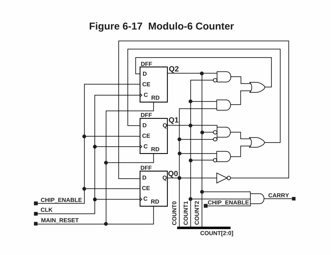
Figure 6-17 Modulo-6 Counter
M0 R P2 7 $ 1 N
M1 RD
P2 4
HA
$ 1 N P3 0
HB
$ 1 N L OS
$ 1 N8 1
WI N P3 4
HD
GND $ 1 N $ 1 N
D2 _1
P3 8 P3 9
HF
P4 0 $ 1 N
HG
P4 2 P4 3
HH
RST
DPGM
P4 6
BCL
P2 3
U5 1 GA D1 _1
GC $ 1 N2 1
D2 _2
$ 4 -$ 1 N7
GG GH
P4 7
P4 8
P2 2
P2 1 F A D1 _2
FC F D Q1 $ 4 -$ 1 N9
FG FH
U2 9
P4 9
P2 0
U5 5 EA $ 1 1- ROL L _
ROLL
ED Q0 $ 2 -$ 1 N2 8
EG EH
P5 0
P5 1
P1 9
VCC
P1 7 DA RB DC DD Q3 $ 2 -$ 1 N7
$ 1 N2 6
DH
U2 5
VCC
P5 3
$ 1 N5 1
P1 5 CA CB CC $ 1 N2 3
Q2 $ 1 N2 7
$ 1 N2 4
CH
P5 4
P5 5
$ 1 N5
U6 1 BA BB $ 1 1- $ 1N1 7
$ 1 1- $ 1N2 9
$ 1 1- A_NEX
$ 1 1- $ 1N2 3
BG BH
U2 1
P5 6
P1 3
$ 1 N6
CL K_ I N
AB $ 1 1- $ 1N3 1
$ 1 1- $ 1N4 3
$ 1 1- B_NEX
AF AG AH
P5 7
P5 8
TCL
GAME_ RESE
PWRDN
P9 P8 P7 P6 P5 P4 P3 P2 GND P6 8 P6 7 P6 6 P6 5 P6 4 P6 3 P6 2
P5 9
P6 1 CCLK
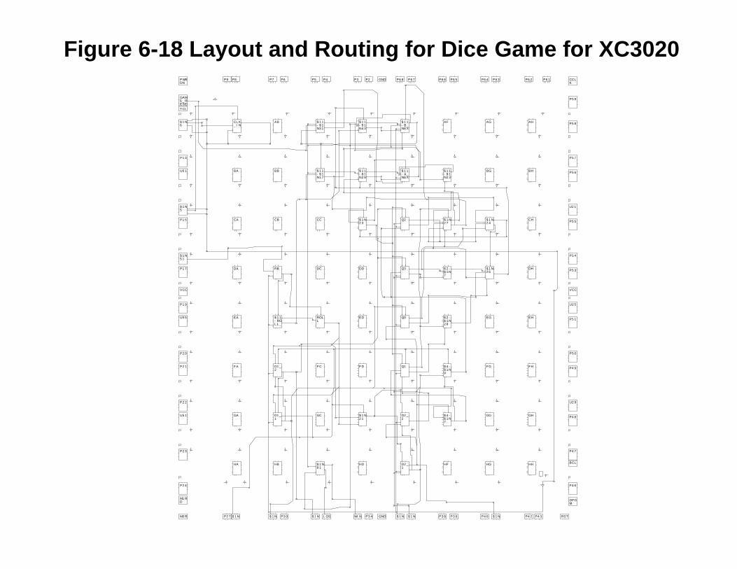
Figure 6-18 Layout and Routing for Dice Game for XC3020
bcdef
bcdef
Z0
Z1
Z
a
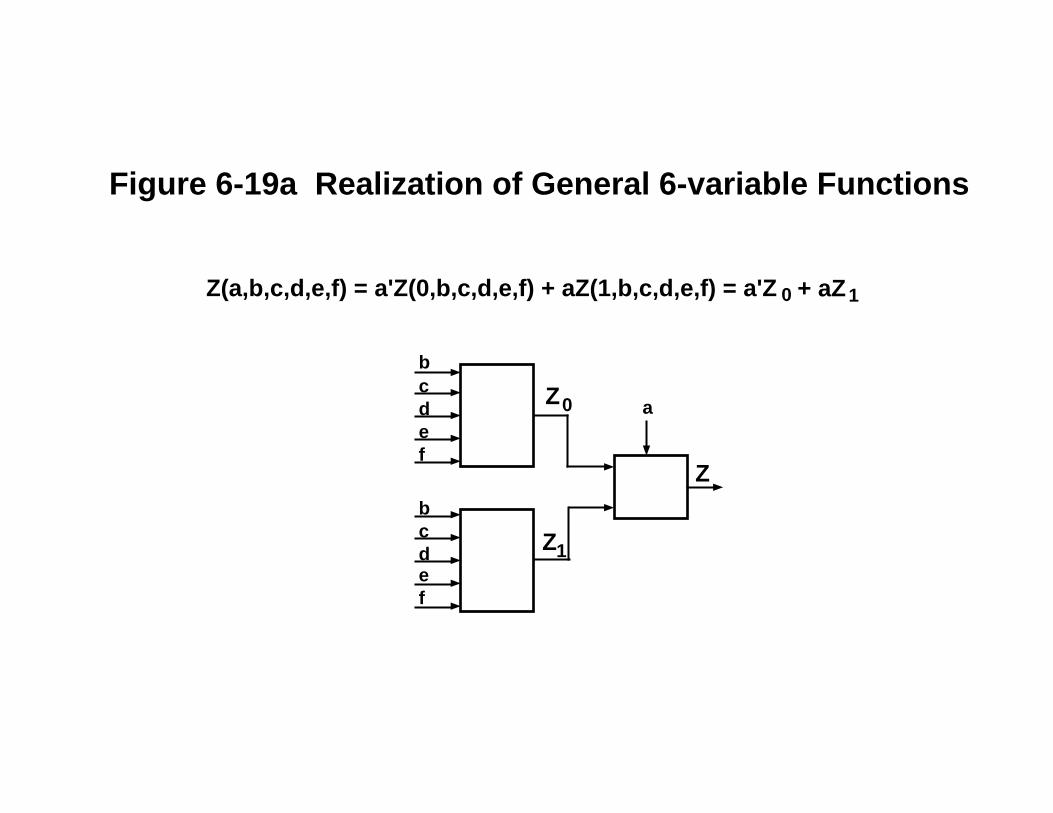
Figure 6-19a Realization of General 6-variable Functions
Z(a,b,c,d,e,f) = a'Z(0,b,c,d,e,f) + aZ(1,b,c,d,e,f) = a'Z + aZ0 1
cdefg
Y0
Y1
Y2
Y3
Z 0
ab
Z
ab
cdefgcdefgcdefg
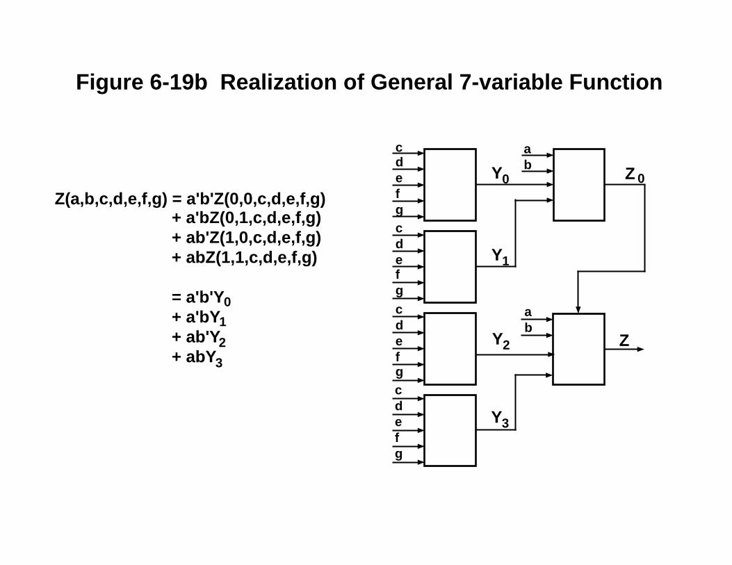
Figure 6-19b Realization of General 7-variable Function
Z(a,b,c,d,e,f,g) = a'b'Z(0,0,c,d,e,f,g)+ a'bZ(0,1,c,d,e,f,g)+ ab'Z(1,0,c,d,e,f,g)+ abZ(1,1,c,d,e,f,g)
= a'b'Y+ a'bY+ ab'Y+ abY
0
1
2
3
1HF
GH
1
SDD Q
ECRD
YQ
S/RCONTROL
K(CLOCK)
F1
F2
F3
F4LOGICFUNCTIONOFF1-F4
F
G1
G2
G3
G4LOGICFUNCTIONOFG1-G4
G
DINFGH
DINFGH
S/RCONTROL
SDD Q
ECRD
XQ
X
Y
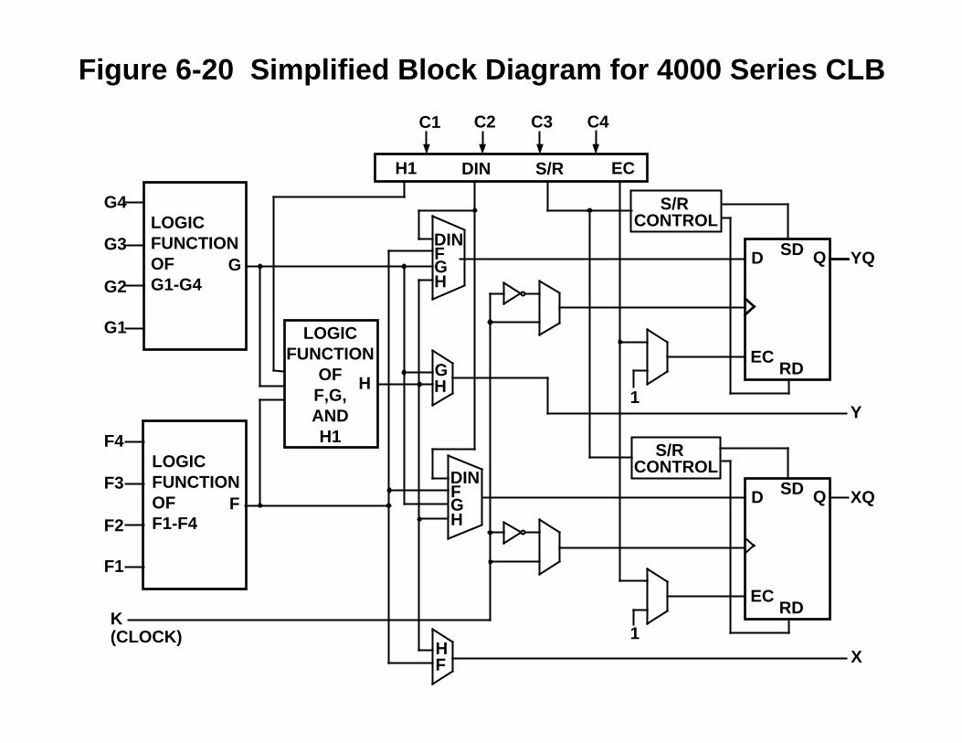
C1 C2 C3 C4
ECS/RDINH1
LOGICFUNCTION
OFF,G,ANDH1
H
Figure 6-20 Simplified Block Diagram for 4000 Series CLB
GCARRY
G
FCARRY
F
M1
M2
M3
M4
C IN UP COUT
H
S/RD Q
EC
S/RD Q
EC
DINHGF
DINHGF
H
F
G
H
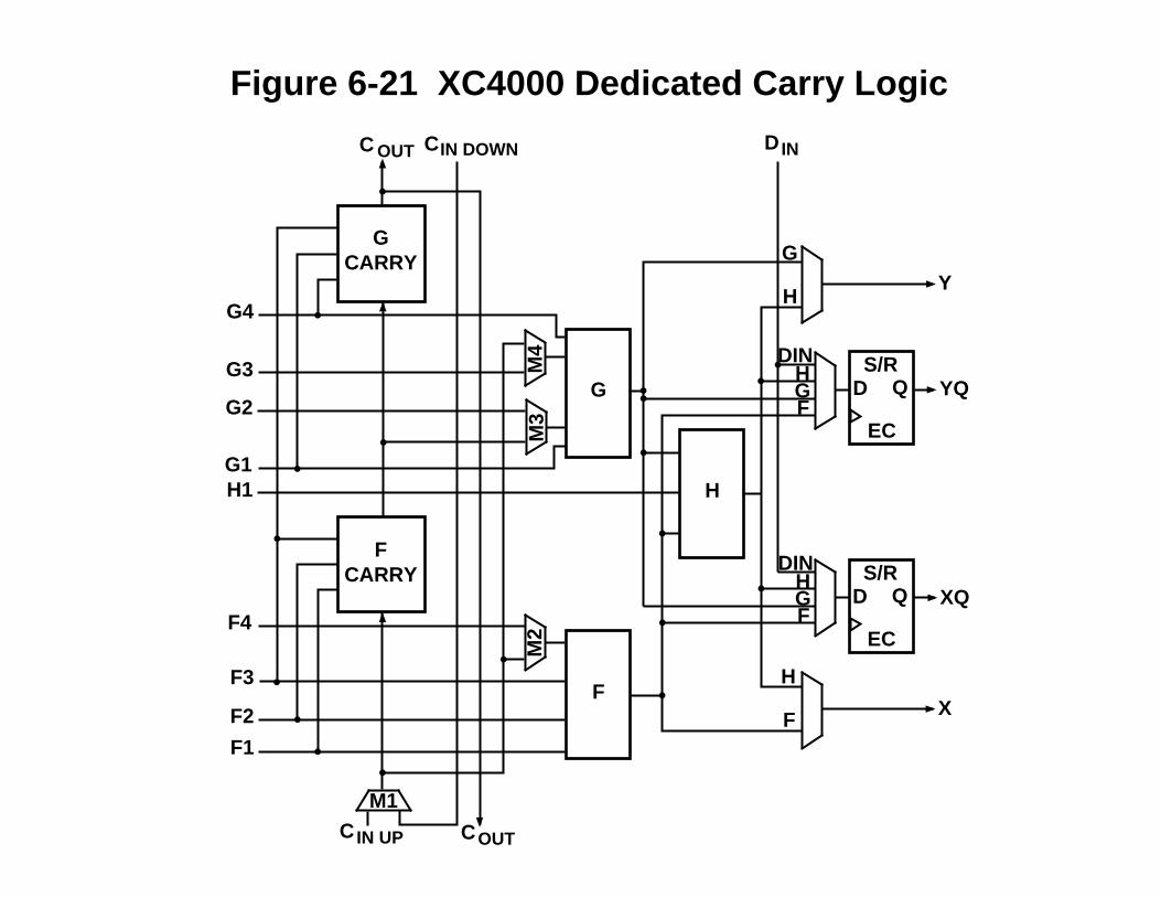
C OUT CIN DOWN D IN
F4
F3
F2
F1
H1G1
G2
G3
G4Y
YQ
XQ
X
Figure 6-21 XC4000 Dedicated Carry Logic
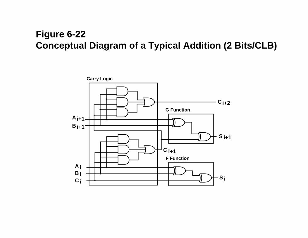
Ai+1Bi+1
A iB iC i
C i+2
S i+1
S i
Carry Logic
G Function
F Function
C i+1
Figure 6-22Conceptual Diagram of a Typical Addition (2 Bits/CLB)
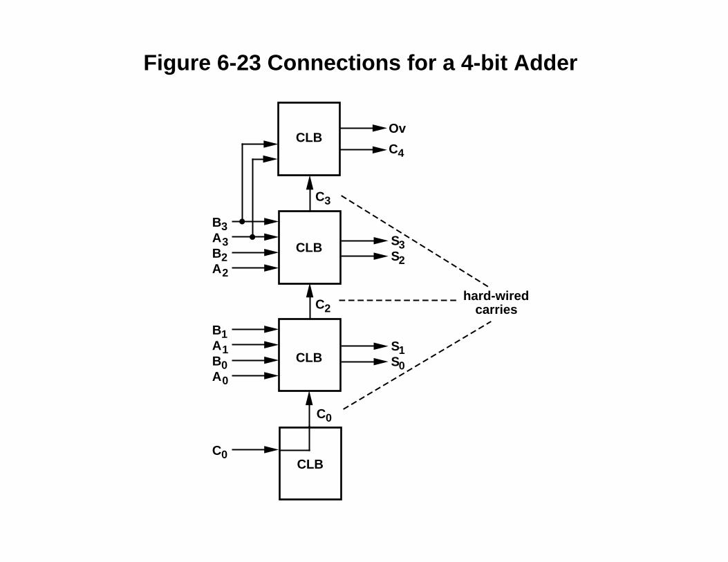
A3
B3
B2A2
C3
A1
B1
B0A0
C2
Ov
C4
C0
hard-wiredcarries
S3S2
CLB
CLB
CLB
CLB
S1S0
C0
Figure 6-23 Connections for a 4-bit Adder
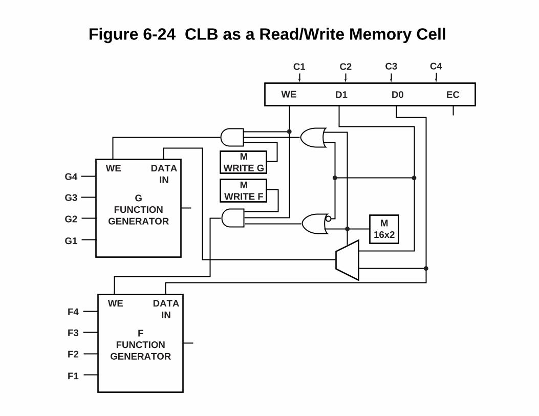
M16x2
MWRITE G
MWRITE F
WE D1 D0 EC
C4C3C2C1
WE DATAIN
GFUNCTION
GENERATOR
G4
G3
G2
G1
WE DATAIN
FFUNCTION
GENERATOR
F4
F3
F2
F1
Figure 6-24 CLB as a Read/Write Memory Cell
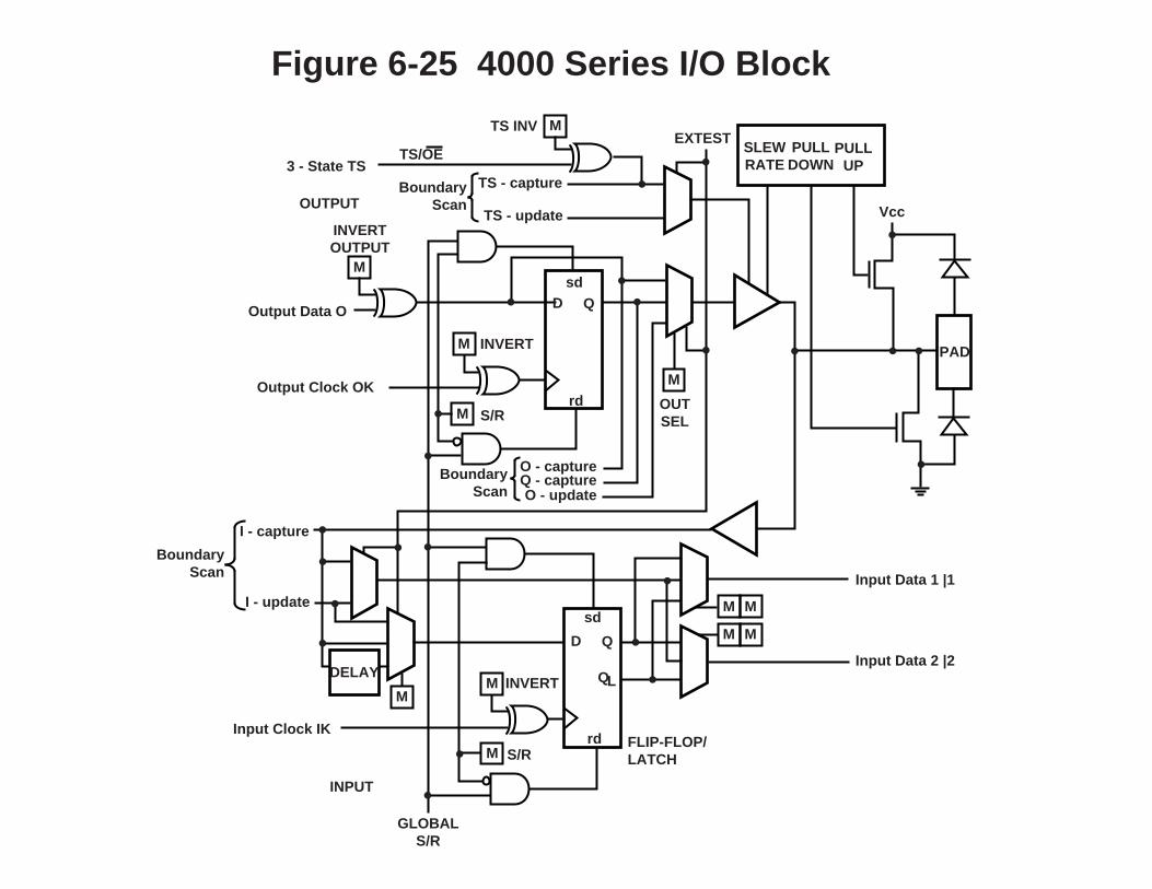
MTS INV
M
INVERTOUTPUT
M INVERT
M S/ROUTSEL
M
BoundaryScan
O - captureQ - captureO - update
M M
M M
M INVERT
M S/R
M
DELAY
Input Data 1 |1
Input Data 2 |2
FLIP-FLOP/LATCH
GLOBALS/R
Vcc
PAD
SLEWRATE
PULLDOWN
PULLUP
EXTEST
TS - capture
TS - update
BoundaryScan
3 - State TSTS/OE
OUTPUT
Output Data O
Output Clock OK
BoundaryScan
I - capture
I - update
Input Clock IK
INPUT
sdD Q
rd
sd
D Q
rd
QL
Figure 6-25 4000 Series I/O Block
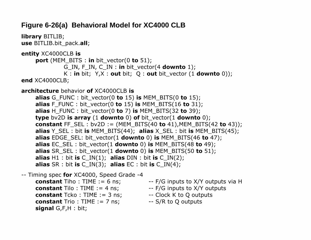
Figure 6-26(a) Behavioral Model for XC4000 CLBlibrary BITLIB;use BITLIB.bit_pack.all;
entity XC4000CLB isport (MEM_BITS : in bit_vector(0 to 51);
G_IN, F_IN, C_IN : in bit_vector(4 downto 1);K : in bit; Y,X : out bit; Q : out bit_vector (1 downto 0));
end XC4000CLB;
architecture behavior of XC4000CLB isalias G_FUNC : bit_vector(0 to 15) is MEM_BITS(0 to 15);alias F_FUNC : bit_vector(0 to 15) is MEM_BITS(16 to 31);alias H_FUNC : bit_vector(0 to 7) is MEM_BITS(32 to 39);type bv2D is array (1 downto 0) of bit_vector(1 downto 0);constant FF_SEL : bv2D := (MEM_BITS(40 to 41),MEM_BITS(42 to 43));alias Y_SEL : bit is MEM_BITS(44); alias X_SEL : bit is MEM_BITS(45);alias EDGE_SEL: bit_vector(1 downto 0) is MEM_BITS(46 to 47);alias EC_SEL : bit_vector(1 downto 0) is MEM_BITS(48 to 49);alias SR_SEL : bit_vector(1 downto 0) is MEM_BITS(50 to 51);alias H1 : bit is C_IN(1); alias DIN : bit is C_IN(2);alias SR : bit is C_IN(3); alias EC : bit is C_IN(4);
-- Timing spec for XC4000, Speed Grade -4constant Tiho : TIME := 6 ns; -- F/G inputs to X/Y outputs via Hconstant Tilo : TIME := 4 ns; -- F/G inputs to X/Y outputsconstant Tcko : TIME := 3 ns; -- Clock K to Q outputsconstant Trio : TIME := 7 ns; -- S/R to Q outputssignal G,F,H : bit;

Figure 6-26(b) Behavioral Model for XC4000 CLBbegin
G <= G_FUNC (vec2int(G_IN)); F <= F_FUNC (vec2int(F_IN));H <= H_FUNC (vec2int(H1&G&F)) after (Tiho-Tilo);X <= (X_SEL and H) or (not X_SEL and F) after Tilo;Y <= (Y_SEL and H) or (not Y_SEL and G) after Tilo;process (K, SR) -- update FF outputsvariable DFF_EC,D : bit_vector(1 downto 0);begin
for i in 0 to 1 loopDFF_EC(i) := EC or EC_SEL(i);case FF_SEL(i) is
when "00" => D(i) := DIN; when "01" => D(i) := F;when "10" => D(i) := G; when "11" => D(i) := H;
end case;if (SR='1') then Q(i)<=SR_SEL(i) after Trio;-- If SR set, then set or reset ffelse
if (DFF_EC(i)='1') then -- If clock enabled then-- If correct triggering edge then update ff valueif ((EDGE_SEL(i)='1' and rising_edge(K)) or (EDGE_SEL(i)='0'
and falling_edge(K))) then Q(i)<=D(i) after Tcko; end if;end if;
end if;end loop;
end process;end behavior;
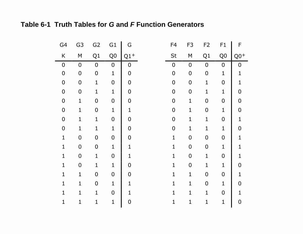
Table 6-1 Truth Tables for G and F Function Generators
G4 G3 G2 G1 G F4 F3 F2 F1 F
K M Q1 Q0 Q1+ St M Q1 Q0 Q0+
0 0 0 0 0 0 0 0 0 00 0 0 1 0 0 0 0 1 10 0 1 0 0 0 0 1 0 10 0 1 1 0 0 0 1 1 00 1 0 0 0 0 1 0 0 00 1 0 1 1 0 1 0 1 00 1 1 0 0 0 1 1 0 10 1 1 1 0 0 1 1 1 01 0 0 0 0 1 0 0 0 11 0 0 1 1 1 0 0 1 11 0 1 0 1 1 0 1 0 11 0 1 1 0 1 0 1 1 01 1 0 0 0 1 1 0 0 11 1 0 1 1 1 1 0 1 01 1 1 0 1 1 1 1 0 11 1 1 1 0 1 1 1 1 0
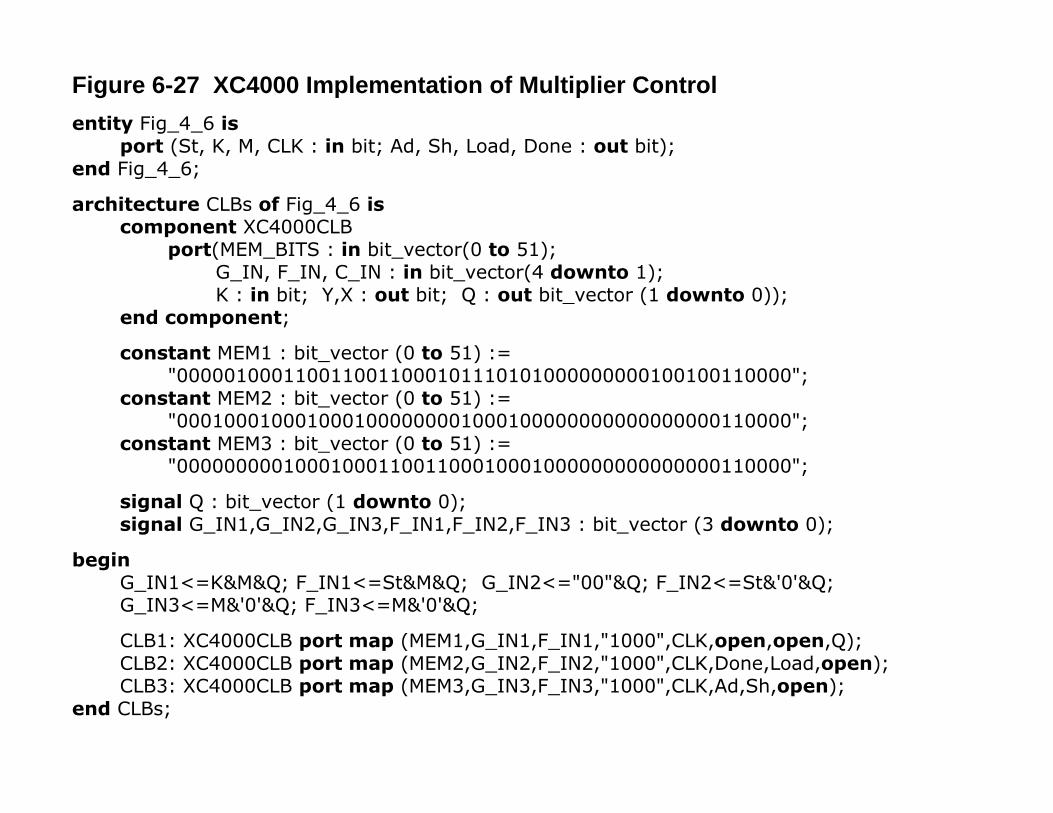
Figure 6-27 XC4000 Implementation of Multiplier Controlentity Fig_4_6 is
port (St, K, M, CLK : in bit; Ad, Sh, Load, Done : out bit);end Fig_4_6;
architecture CLBs of Fig_4_6 iscomponent XC4000CLB
port(MEM_BITS : in bit_vector(0 to 51);G_IN, F_IN, C_IN : in bit_vector(4 downto 1);K : in bit; Y,X : out bit; Q : out bit_vector (1 downto 0));
end component;
constant MEM1 : bit_vector (0 to 51) :="0000010001100110011000101110101000000000100100110000";
constant MEM2 : bit_vector (0 to 51) :="0001000100010001000000001000100000000000000000110000";
constant MEM3 : bit_vector (0 to 51) :="0000000001000100011001100010001000000000000000110000";
signal Q : bit_vector (1 downto 0);signal G_IN1,G_IN2,G_IN3,F_IN1,F_IN2,F_IN3 : bit_vector (3 downto 0);
beginG_IN1<=K&M&Q; F_IN1<=St&M&Q; G_IN2<="00"&Q; F_IN2<=St&'0'&Q;G_IN3<=M&'0'&Q; F_IN3<=M&'0'&Q;
CLB1: XC4000CLB port map (MEM1,G_IN1,F_IN1,"1000",CLK,open,open,Q);CLB2: XC4000CLB port map (MEM2,G_IN2,F_IN2,"1000",CLK,Done,Load,open);CLB3: XC4000CLB port map (MEM3,G_IN3,F_IN3,"1000",CLK,Ad,Sh,open);
end CLBs;
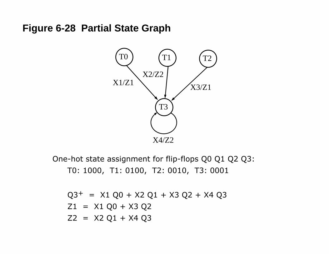
Figure 6-28 Partial State Graph
T0
T3
T1 T2
X1/Z1X2/Z2
X3/Z1
X4/Z2
One-hot state assignment for flip-flops Q0 Q1 Q2 Q3:T0: 1000, T1: 0100, T2: 0010, T3: 0001
Q3+ = X1 Q0 + X2 Q1 + X3 Q2 + X4 Q3Z1 = X1 Q0 + X3 Q2Z2 = X2 Q1 + X4 Q3

INPUT/GCLKINPUT/GCLRn
INPUT/OE1INPUT/OE2
8 to 16I/O pins
I/OControlBlock
Macrocells1 to 8
Macrocells9 to 16
8 to16
LAB A
36
16
8 to 16
Macrocells33 to 40
Macrocells41to 48
8 to16
LAB C
36
16
8 to 16
8 to 16I/O pins
I/OControlBlock
8 to 16I/O pins
I/OControlBlock
8 to 16I/O pins
I/OControlBlock
Macrocells17 to 24
Macrocells25 to 32
8 to16
LAB B
36
16
8 to 16
Macrocells49 to 56
Macrocells57 to 64
8 to16
LAB D
36
16
8 to 16
PIA
Figure 6-29 Altera 7000 Series Architecturefor EPM7032, 7064, and 7096 Devices
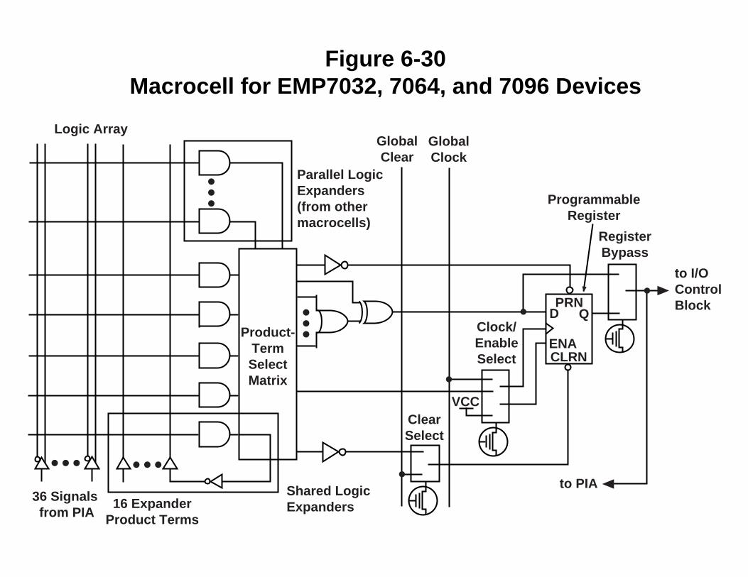
Logic Array
Parallel LogicExpanders(from othermacrocells)
GlobalClear
GlobalClock
Product-TermSelectMatrix
36 Signals from PIA
16 ExpanderProduct Terms
Shared LogicExpanders
ClearSelect
VCC
Clock/EnableSelect
ENACLRN
PRND Q
to PIA
to I/OControlBlock
RegisterBypass
ProgrammableRegister
Figure 6-30Macrocell for EMP7032, 7064, and 7096 Devices
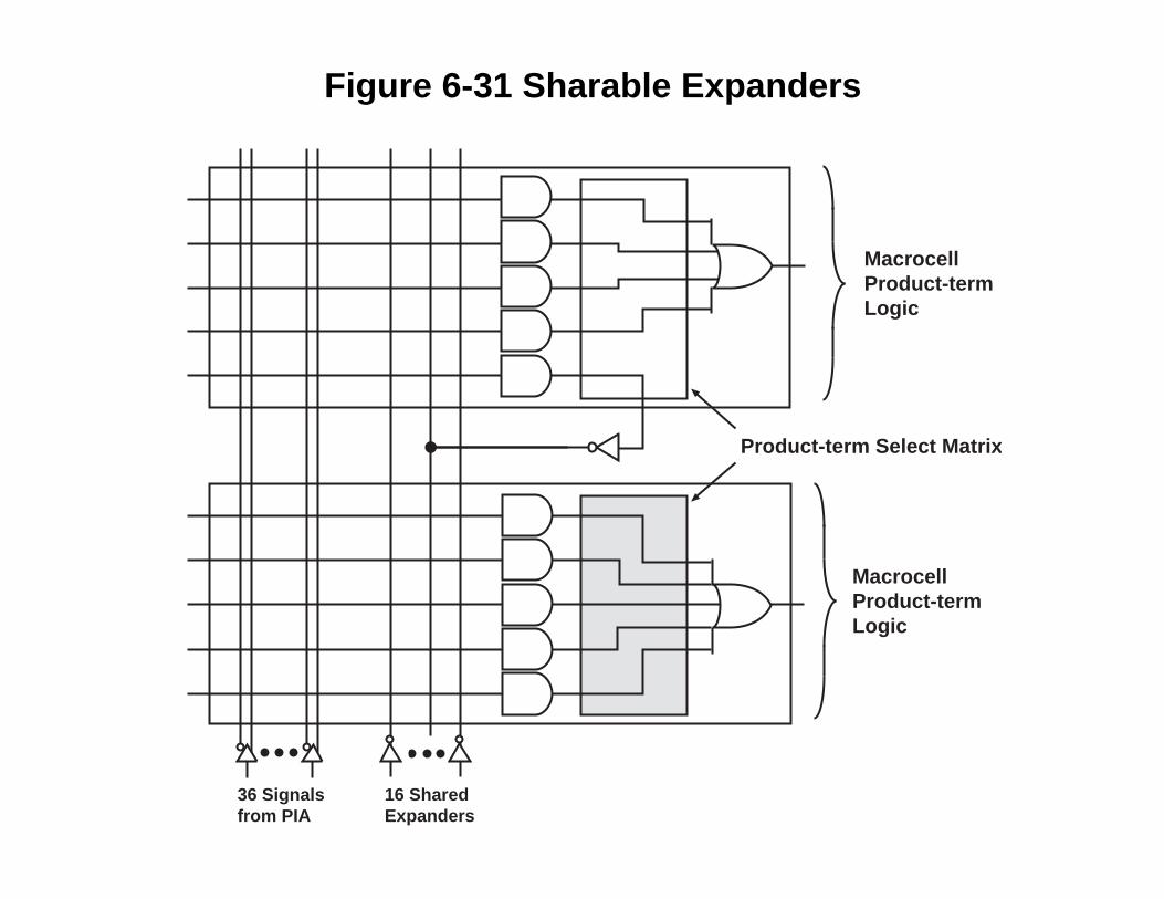
MacrocellProduct-termLogic
Product-term Select Matrix
MacrocellProduct-termLogic
36 Signalsfrom PIA
16 SharedExpanders
Figure 6-31 Sharable Expanders

Expanders
Preset
Clock
Clear
Product-TermSelectMatrix
Preset
Clock
Clear
Product-TermSelectMatrix
36 Signalsfrom PIA
16 Shared
MacrocellProduct-termLogic
MacrocellProduct-termLogic
from Previous Macrocell
to NextMacrocell
Figure 6-32 Parallel Expanders

OE1nOE2n
VCC
GND
OE Control
to PIA
from Macrocell
Figure 6-33 I/O Block for EPM7032, 7064, and 7096
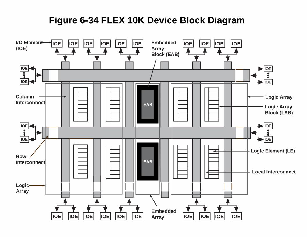
I/O Element(IOE)
Logic ArrayBlock (LAB)
IOEIOE
IOEIOE
EmbeddedArrayBlock (EAB)
RowInterconnect
Logic Array
IOEIOE
IOEIOEEmbeddedArray
IOE
IOE
IOE
Local Interconnect
IOEIOE
IOEIOE
IOEIOE
IOEIOE
IOEIOE
IOEIOE
Logic Element (LE)
ColumnInterconnect
IOE
IOE
IOE
IOE
IOE
EAB
EAB
LogicArray
Figure 6-34 FLEX 10K Device Block Diagram
Figure 6-35 FLEX 10K Logic Array Block
28
Carry-In &Cascade-In
LE1
LE8
LE2
LE3
LE4
LE5
LE6
LE7
ColumnInterconnect
Row Interconnect
LAB LocalInterconnect
Column-to-RowInterconnect
Carry-Out &Cascade-Out
16
24LAB ControlSignals
6
Dedicated Inputs &Global Signals
16
4
8
4
4
4
4
4
4
4
4
4
4 2 8

to LAB LocalInterconnect
LABCTRL3
LABCTRL4
DATA1DATA2DATA3DATA4
LABCTRL1LABCTRL2
Carry-In
ClockSelect
Carry-Out
Look-UpTable(LUT)
Clear/PresetLogic
CarryChain
CascadeChain
Cascade-In
Cascade-Out
to FastTrackInterconnect
ProgrammableRegister
PRn
CLRn
D Q
ENA
Register Bypass
Device-WideClear
Figure 6-36 FLEX 10K Logic Element

d[3..0]LE1
LUT
d[7..4]LE2
LUT
d[(4n-1)..(4n-4)]LEn
LUT
d[3..0] LUT
d[7..4] LUT
d[(4n-1)..(4n-4)] LUT
LE1
LE2
LEn
AND Cascade Chain OR Cascade Chain
Figure 6-37 Cascade Chain Operation

D
D Q
Columninterconnect
Row Interconnect
RAM/ROM256 x 8512 x 4
1,024 x 22,048 x 1
WE
Address
DataIn
8, 4, 2, 1
EAB Local Interconnect
Dedicated Inputs & Global Signals
6
D Q
D Q
D QDataOut
24
Device-WideClear
8, 9, 10, 11
2, 4, 8, 16
2, 4, 8, 16
Figure 6-38 FLEX 10K Embedded Array Block