Integrated Multi-Channel DC-DC Converter for TFT LCD...
20
1 FP6787-1.2-NOV-2009 FP6787/A fitipower integrated technology lnc. Integrated Multi-Channel DC-DC Converter for TFT LCD Panel Description The FP6787/A offers a compact power supply solution to provide all voltages required by thin-film transistor (TFT) LCD panel. The FP6787/A includes a high performance boost regulator, a low dropout linear regulator (LDO), a voltage detector, a VCOM buffer (unity-gain OPA), a positive charge pump and a negative charge pump to provide adjustable regulated output voltages. The boost converter provides the regulated supply voltage for the panel source driver ICs. The converter is a 640kHz current-mode regulator with an integrated 16V N-Channel 0.2Ω MOSFET. It provides fast transient response to pulsed loading while achieving efficiency over 85%. The device can produce output voltage as high as 14V from an input as low as 2.7V. FP6787/A includes internal 8ms soft start. The low dropout (LDO) linear regulator can supply up to 600mA current while input voltage is 5V. It uses an internal PMOS as the pass device. It is suitable for the supply voltage of the timing controller. The voltage detector monitors the supply voltage to issue a reset signal while the detected voltage is too low. The detecting level is decided by an external resistor divider and the delay time is programmable by an external capacitor. The VCOM buffer can drive the LCD VCOM voltage that features high short-circuit current (250mA), fast slew rate (12V/μs), wide bandwidth (12MHz) and rail-to-rail inputs and outputs. The positive charge pump controller provides regulated TFT gate-on voltage. The negative charge pump controller provides regulated TFT gate-off voltage. The regulation of the positive and negative charge pump is generated by the internal comparator that senses the output voltage and compares it with an internal voltage reference. Features ● High Efficiency ● Low Power Consumption ● 2.7V to 5.5V Input Supply Voltage 640kHz Current-Mode Boost Regulator ● Fast Transient Response to Pulsed Load ● Adjustable Output Voltage with ±1% Accuracy ● Built-In 16V, 3A, 0.2Ω N-Channel MOSFET ● High Efficiency up to 85% ● Built-in 8ms Soft-Start ● Over-Current Protection ● Over-Voltage Protection Low Dropout Linear Regulator ● 600mA Maximum Output Current ● Fixed Output Voltage : 3.3V (FP6787)and 2.5V (FP6787A) ● ±2% Output Voltage Accuracy Low Voltage Detector ● Programmable Detection Voltage ● ±2% Detection Voltage Accuracy ● Programmable Reset Delay Time ● Push-Pull Output Unity-Gain Operation Amplifier for VCOM Buffer ● Rail-to-Rail Input and Output ● 12V/μs Slew Rate and 12MHz Bandwidth ● 250mA Short-Circuit Current ● Charge Pump for VGH Regulation ● Charge Pump for VGL Regulation ● Over-Temperature Protection ● TSSOP-20 And TQFN-20 Exposed Pad Packages ● RoHS Compliant Applications ● Notebook Computers Displays ● LCD Monitor Panels
Transcript of Integrated Multi-Channel DC-DC Converter for TFT LCD...

1 FP6787-1.2-NOV-2009
FP6787/Afitipower integrated technology lnc.
Integrated Multi-Channel DC-DC Converterfor TFT LCD Panel
Description
The FP6787/A offers a compact power supply solution to provide all voltages required by thin-film transistor (TFT) LCD panel. The FP6787/A includes a high performance boost regulator, a low dropout linear regulator (LDO), a voltage detector, a VCOM buffer (unity-gain OPA), a positive charge pump and a negative charge pump to provide adjustable regulated output voltages.
The boost converter provides the regulated supply voltage for the panel source driver ICs. The converter is a 640kHz current-mode regulator with an integrated 16V N-Channel 0.2Ω MOSFET. It provides fast transient response to pulsed loading while achieving efficiency over 85%. The device can produce output voltage as high as 14V from an input as low as 2.7V. FP6787/A includes internal 8ms soft start.
The low dropout (LDO) linear regulator can supply up to 600mA current while input voltage is 5V. It uses an internal PMOS as the pass device. It is suitable for the supply voltage of the timing controller.
The voltage detector monitors the supply voltage to issue a reset signal while the detected voltage is too low. The detecting level is decided by an external resistor divider and the delay time is programmable by an external capacitor.
The VCOM buffer can drive the LCD VCOM voltage that features high short-circuit current (250mA), fast slew rate (12V/µs), wide bandwidth (12MHz) and rail-to-rail inputs and outputs.
The positive charge pump controller provides regulated TFT gate-on voltage. The negative charge pump controller provides regulated TFT gate-off voltage. The regulation of the positive and negative charge pump is generated by the internal comparator that senses the output voltage and compares it with an internal voltage reference.
Features High Efficiency Low Power Consumption 2.7V to 5.5V Input Supply Voltage
640kHz Current-Mode Boost Regulator Fast Transient Response to Pulsed Load Adjustable Output Voltage with ±1% Accuracy Built-In 16V, 3A, 0.2Ω N-Channel MOSFET High Efficiency up to 85% Built-in 8ms Soft-Start Over-Current Protection Over-Voltage Protection
Low Dropout Linear Regulator 600mA Maximum Output Current Fixed Output Voltage : 3.3V (FP6787)and 2.5V
(FP6787A) ±2% Output Voltage Accuracy
Low Voltage Detector Programmable Detection Voltage ±2% Detection Voltage Accuracy Programmable Reset Delay Time Push-Pull Output
Unity-Gain Operation Amplifier for VCOM
Buffer Rail-to-Rail Input and Output 12V/µs Slew Rate and 12MHz Bandwidth 250mA Short-Circuit Current
Charge Pump for VGH Regulation Charge Pump for VGL Regulation Over-Temperature Protection TSSOP-20 And TQFN-20 Exposed Pad
Packages RoHS Compliant
Applications Notebook Computers Displays LCD Monitor Panels

2 FP6787-1.2-NOV-2009
FP6787/Afitipower integrated technology lnc.
Pin Assignments TP Package (TSSOP-20 Exposed Pad)
12345678910
20191817161514131211
LX
OPAO
OPAI
LDOO
LDOI
AGND
FBP
FB
COMP
FBN
PGND
DRVN
AVDDI
VIN
AVDDO
RESETB
VDIV
CD
REF
DRVP
PGND
WQ Package (TQFN-20, 4mm x 4mm)
Figure1. Pin Assignment of FP6787/A
Ordering Information
Typical Application Circuit
Figure2. Typical Application Circuit of FP6787/A
TR: Tape / Reel
Package Type TP: TSSOP-20 (EP) WQ: TQFN-20 (4X4)
G: Green
FP6787
LDO Output Voltage Blank: 3.3V A: 2.5V
3 FP6787-1.2-NOV-2009
FP6787/Afitipower integrated technology lnc.
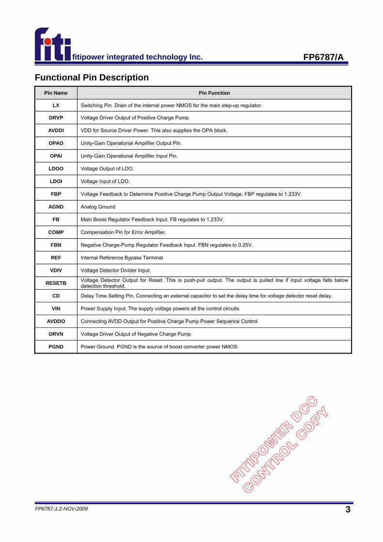
Functional Pin Description Pin Name Pin Function
LX Switching Pin. Drain of the internal power NMOS for the main step-up regulator.
DRVP Voltage Driver Output of Positive Charge Pump.
AVDDI VDD for Source Driver Power. This also supplies the OPA block.
OPAO Unity-Gain Operational Amplifier Output Pin.
OPAI Unity-Gain Operational Amplifier Input Pin.
LDOO Voltage Output of LDO.
LDOI Voltage Input of LDO.
FBP Voltage Feedback to Determine Positive Charge Pump Output Voltage. FBP regulates to 1.233V.
AGND Analog Ground
FB Main Boost Regulator Feedback Input. FB regulates to 1.233V.
COMP Compensation Pin for Error Amplifier.
FBN Negative Charge-Pump Regulator Feedback Input. FBN regulates to 0.25V.
REF Internal Reference Bypass Terminal.
VDIV Voltage Detector Divider Input.
RESETB Voltage Detector Output for Reset. This is push-pull output. The output is pulled low if input voltage falls below detection threshold.
CD Delay Time Setting Pin. Connecting an external capacitor to set the delay time for voltage detector reset delay.
VIN Power Supply Input. The supply voltage powers all the control circuits.
AVDDO Connecting AVDD Output for Positive Charge Pump Power Sequence Control
DRVN Voltage Driver Output of Negative Charge Pump
PGND Power Ground. PGND is the source of boost converter power NMOS.

4 FP6787-1.2-NOV-2009
FP6787/Afitipower integrated technology lnc.
Absolute Maximum Ratings LX, AVDDI, AVDDO, OPAI, OPAO, DRVP, DRVN -------------------------------------------------------- - 0.3V to 18V
CD, RESETB, VDIV, COMP, FB, FBP, FBN, REF--------------------------------------------------------- - 0.3V to 6V
VIN, LDOI, LDOO-------------------------------------------------------------------------------------------------- - 0.3V to 6V
PGND, AGND------------------------------------------------------------------------------------------------------- - 0.3V to 0.3V
Power Dissipation @ TA=25:
TSSOP-20(Exposed Pad)----------------------------------------------------------------------------- 1.38W
TQFN-20 (4mmx4mm)--------------------------------------------------------------------------------- 1.1W
Package Thermal Resistance (θJA):
TSSOP-20 (Exposed Pad) --------------------------------------------------------------------------- 40/W
TQFN-20 (4mmx4mm) -------------------------------------------------------------------------------- 50/W
Lead Temperature (Soldering, 10sec.) ----------------------------------------------------------------------- 260
Maximum Junction Temperature (TJ) ------------------------------------------------------------------------- 150
Storage Temperature (TSTG) ------------------------------------------------------------------------------------ -65 to 150
ESD Susceptibility
HBM(Human Body Mode)-------------------------------------------------------------------------------------- 1.5KV
MM(Machine Mode)---------------------------------------------------------------------------------------------- 100V Note1:Stresses beyond those listed under “Absolute Maximum Ratings" may cause permanent damage to the device.
Recommended Operating Conditions Supply Voltage (VIN)---------------------------------------------------------------------------------------------- 2.7V to 5.5V
Output Voltage of Main Boost Converter (VAVDDI)--------------------------------------------------------- VIN to 14V
Operating Temperature Range-------------------------------------------------------------------------------- -40 to 85

5 FP6787-1.2-NOV-2009
FP6787/Afitipower integrated technology lnc.
Block Diagram
Figure3. Block Diagram of FP6787/A

6 FP6787-1.2-NOV-2009
FP6787/Afitipower integrated technology lnc.
Electrical Characteristics
(VIN=5V, VAVDDI=10V, TA=25°C, unless otherwise specified)
Parameter Symbol Conditions Min Typ Max Unit
System Supply
Input Voltage Range VIN 2.7 5.5 V
VIN Rising 2.3 2.5 2.7 VIN UVLO Threshold VUVLO
Hysteresis 0.2 V
VIN Supply Current IIN VFB= VFBP =1.4V VFBN=0 0.5 1 1.5 mA
REF Output Voltage VREF 1.215 1.233 1.25 V
160 Thermal Shutdown Threshold (Note2) TSD
Hysteresis 20 0C
Boost Regulator
Output Voltage Range VAVDDI VIN VOVP V
Over-Voltage Protection VOVP 14 15 16 V
Operation Frequency FOSC 540 640 740 kHz
Maximum Duty Cycle 85 %
Feedback regulation Voltage VFB No Load, TA=250C 1.221 1.233 1.245 V
Feedback Input Bias Current IFB VFB = 1.5V 10 nA
Transconductance of Error Amplifier Gm ICOMP =5µA 170 µA/V
Voltage Gain of Error Amplifier AV 700 V/V
Switch ON-Resistance RON 0.2 Ω
Switch Current Limit (Note2) ILIM VFB = 1V Duty Cycle=65% 3 A
Switch Leakage Current (Note2) ILX VLX=10V 0.1 µA
Current Sense Transconductance 3.8 S
Soft-Start Time (Note2) TSS 8 ms
Low Dropout Linear Regulator (LDO)
Input Voltage VLDOI 2.8 5.5 V
FP6787 3.234 3.3 3.366 V LDO Output Voltage VLDO
FP6787A 2.45 2.5 2.55 V
FP6787, IOUT=600mA 600 mV Dropout Voltage VDROP
FP6787A, IOUT=600mA 800 mV
Current Limit ILIM 600 mA
Quiescent Current ILDO 10 30 50 µA
Voltage Detector
Minimum Operating Voltage 1.6 V
Detecting Voltage Adjustment VDIV 1.078 1.1 1.122 V
Hysteresis 5 %
CD Pin Charge Current ICD 4.5 5.5 6.5 µA

7 FP6787-1.2-NOV-2009
FP6787/Afitipower integrated technology lnc.
Electrical Characteristics (Continued)
(VIN=5V, VAVDDI=10V, TA=25°C, unless otherwise specified) Parameter Symbol Conditions Min Typ Max Unit
VCOM Buffer
Supply Voltage Range 4.5 16 V
Supply Current IOP 1.2 mA
Input Offset Voltage VOS VCOM= VAVDDI/2, TA=250C -30 30 mV
Input Bias Current IBIAS -50 0 50 nA
IOUT=100uA AVDDI-5 AVDDI-15 mV Output Voltage Swing High VOH
IOUT=5mA AVDDI-80 AVDDI-150 mV
IOUT=-100uA 5 15 mV Output Voltage Swing Low VOL IOUT=5mA 80 150 mV
Short-Circuit Current To VAVDDI/2, Source & Sink 150 250 mA
Output Source & Sink Current To VAVDDI/2, Source & Sink 40 mA
-3dB Bandwidth F3DB 12 MHz
Gain Bandwidth Product GBW 8 MHz
Slew Rate SR 12 V/µs
Positive Charge Pump
FBP Reference Voltage VFBP IDRVP=100µA 1.202 1.233 1.264 V
FBP Input Bias Current IFBP VFBP=1.4V -50 0 50 nA
DRVP PCH On-Resistance IOUT=20mA 8 Ω
DRVP NCH On-Resistance IOUT=20mA 1.1 Ω
Switching Frequency 540 640 740 kHz
Soft-Start Time TSSP 8 ms
Negative Charge Pump
FBN Reference Voltage VFBN IDRVN=100µA 235 250 265 mV
FBN Input Bias Current IFBN VFBN=0V -50 0 50 nA
DRVN PCH On-Resistance IOUT=20mA 4.4 Ω
DRVN NCH On-Resistance IOUT=20mA 2.6 Ω
Switching Frequency 540 640 740 kHz
Soft-Start Time (Note2) TSSN 5 ms
Note2: Guaranteed by design.

8 FP6787-1.2-NOV-2009
FP6787/Afitipower integrated technology lnc.
Typical Performance Curves
Figure4. Power-up Sequence Figure5. Boost Converter Power-up waveform
Figure6. Boost Converter Power-up waveform Figure7. Boost Converter Load Transient Response (0 300mA)
Figure8. Boost converter Over-Voltage Protection
Waveform. Figure9. Charge Pumps Power-up Sequence
CH1:VIN
CH2:VREF
CH3:VLDOO
CH4:VAVDD
CH1:VIN
CH2: VAVDDI
CH4: IINDUCTOR
CH1:VIN
CH2: VAVDDI
CH4:Inductor Current
CH1: VAVDDI
CH4:ILOAD
CH1: VAVDDI
CH2: VFB
CH1:VIN
CH2: VAVDDI
CH3:VGH
CH4:VGL

9 FP6787-1.2-NOV-2009
FP6787/Afitipower integrated technology lnc.
Typical Performance Curves (Continued)
Figure10. VGL operation waveform (Output Current =0mA) Figure11.VGH operation waveform (Output Current =0mA)
Figure12. Unit-Gain Small-Signal Step Response Figure13. Unit-Gain Small-Signal Sine wave Response
Figure14. Unit-Gain Large-Signal Step Response Figure15. Unit-Gain Large-Signal Sine wave Response
CH1:VGL
CH2: VDRVN
CH4:IVGL
CH1:VGH
CH2: VDRVP
CH4:IVGH
CH1:OPAI
CH2: OPAO
CH1:OPAI
CH2: OPAO
CH1:OPAI
CH2: OPAO
CH1:OPAI
CH2: OPAO

10 FP6787-1.2-NOV-2009
FP6787/Afitipower integrated technology lnc.
Typical Performance Curves (Continued)
Figure16. Unit-Gain Sink 150mA dynamic load transient Figure17. Unit-Gain Source 150mA dynamic load transient
Figure18. LDO Load Transient Response Figure19. LDO Line Transient Response
Figure20. Reset Power on Figure21. Reset Power off
CH1:OPAO
CH4: ILOAD
CH1:VLDOO
CH4: ILOAD (0 300mA)
CH1:OPAO
CH4: ILOAD
CH1:VLDOI (3V 5V)
CH2: VLDOO
CH1:VIN
CH2: VRESETB
CH1:VIN
CH2: VRESETB

11 FP6787-1.2-NOV-2009
FP6787/Afitipower integrated technology lnc.
Typical Performance Curves (Continued)
0 50 100 150 200 250 3001.10
1.12
1.14
1.16
1.18
1.20
1.22
1.24
1.26
1.28
1.30
VREF
(V)
AVDDI Output Current (mA) 3.0 3.5 4.0 4.5 5.0600
610
620
630
640
650
660
670
680
690
700
Freq
uenc
y (K
Hz)
VIN(V)
Figure22. VREF vs. Boost Converter Output Current Figure23. Switching Frequency vs. Vin
-40 -20 0 20 40 60 80 100 1201.10
1.12
1.14
1.16
1.18
1.20
1.22
1.24
1.26
1.28
1.30
VREF
(V)
Temperature(0C) 50 100 150 200 250 300
65
70
75
80
85
90
95
100
Effic
ienc
y (%
)
ILoad (mA)
3V 4V 5V
Figure24. VREF vs. Temperature Figure25. Boost Converter Efficiency
-40 -20 0 20 40 60 80 100 1209.00
9.05
9.10
9.15
9.20
9.25
9.30
9.35
9.40
AVD
DI (
V)
Temperature(0C)
-40 -20 0 20 40 60 80 100 120500
520
540
560
580
600
620
640
660
680
700
Freq
uenc
y (K
Hz)
Temperature(0C)
Figure26. Boost Converter Output Voltage vs. Temperature Figure27.Switching Frequency vs. Temperature

12 FP6787-1.2-NOV-2009
FP6787/Afitipower integrated technology lnc.
Typical Performance Curves (Continued)
3.0 3.5 4.0 4.5 5.01.10
1.12
1.14
1.16
1.18
1.20
1.22
1.24
1.26
1.28
1.30
VRFE
(V)
VIN (V) 3.0 3.5 4.0 4.5 5.0
25
26
27
28
29
30
31
32
33
34
35
Qui
esce
nt C
urre
nt(u
A)
LDOI (V)
Figure28. VREF vs. VIN Figure29. LDO Quiescent Current vs. LDO Input Voltage
0 50 100 150 200 250 3000
50
100
150
200
250
300
350
400
450
500
Dro
pout
Vol
tage
(mV)
Output Current (mA)
-40OC 25OC 85OC
0 50 100 150 200 250 300
2.40
2.44
2.48
2.52
2.56
2.60
Out
put V
olta
ge (V
)
Output Current (mA)
3V 4V 5V
Figure30. LDO Dropout Voltage vs. Output current Figure31. LDO Output Voltage vs. Output Current
0.0 0.5 1.0 1.5 2.0 2.50
20
40
60
80
100
Out
put C
urre
nt (m
A)
NMOS VDS (V) 0.0 0.5 1.0 1.5 2.0 2.5
0
5
10
15
20
Out
put C
urre
nt (m
A)
PMOS VDS (V)
Figure32. Reset Output NMOS Driving Ability Figure33. Reset Output PMOS Driving Ability
13 FP6787-1.2-NOV-2009
FP6787/Afitipower integrated technology lnc.
Typical Performance Curves (Continued)
-40 -20 0 20 40 60 80 100 1204.0
4.2
4.4
4.6
4.8
5.0
5.2
5.4
5.6
5.8
6.0
CD
Pin
Cha
rge
Cur
rent
(uA
)
Temperature(0C)
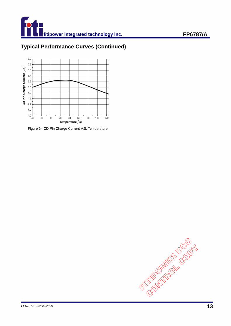
Figure 34.CD Pin Charge Current V.S. Temperature

14 FP6787-1.2-NOV-2009
FP6787/Afitipower integrated technology lnc.
Functional Description
Introduction The FP6787/A represents DC/DC regulator to provide a complete power solution for active matrix thin-film transistor liquid crystal display (TFT-LCD) applications. It contains a high performance boost regulator to generate voltage for the panel source driver ICs, a low dropout (LDO) linear regulator is suitable for supply voltage of the timing controller, a positive charge pump and negative charge pump provide regulated TFT gate-on and gate-off voltage, a unity-gain OPA can drive the VCOM (LCD backplane), and a voltage detector monitors the supply voltage. The FP6787/A also consists of a precision 1.233V reference, current-limited, soft-start, power-up sequencing and thermal shutdown. The following content includes the detailed description and the information of the component selection in the general application circuit as Figure 36 shown.
Boost Regulator The boost regulator can operate in both discontinuous conduction mode (DCM) at light load and continuous conduction mode (CCM). In continuous current mode, current flows continuously in the inductor during entire switching cycle in steady state operation. The voltage conversion ratio in continuous current mode is given by :
D11
VV
IN
AVDDI
−=
Where D is the duty cycle of the switching MOSFET. The boost regulator uses a summing amplifier architecture consisting of gm stages for voltage feedback, current feedback and slop compensation. A comparator looks at the peak inductor current cycle by cycle and terminates the PWM cycle if the current limit is reached. To add higher flexibility to the selection of external component values, the device uses external loop compensation.
Soft Start The FP6787/A provides internal 8ms soft-start function to minimize the inrush current. When power on, a constant current charges an internal capacitor. The inductor peak current will be limited during the charging period. In the meanwhile, the frequency increases slowly at the beginning. When power off, the internal capacitor will be discharged for next soft-start time.
Compensation The boost converter of FP6787/A can be compensated by a RC network connected form COMP pin to ground. The external compensation network consisted of R8, C9, and C10 as figure36 shown. The larger value resistor and lower value capacitor can reduce the transient overshoot, however, at the expense of stability of the loop. R8 is used to set the high-frequency integrator gain for fast transient response. While R8 is decided, C10 is chosen to set the integrator zero to maintain the loop stability. C9 is used to cancel the zero caused by the output capacitor and its ESR.
For each components of external compensation network, the above equations provide the approximate calculations. In order to obtain better transient performance, it is necessary to adjust the component values of external compensation network.
Over Current Protection
The FP6787/A boost converter has over current protection to limit peak inductor current. It prevents inrush current damaging the external component (inductor, diode, capacitor etc.) and IC. When peak inductor current reach current limit during the ON-time, the over current protection function will be work. The action of protection function would terminate the internal LX switch and shortens the duty cycle. When the over current protection is relieved, the chip operates well again. Therefore, the output voltage drops if the over current condition occurs. Actual current limit is always larger than the nominal value because of the internal circuit delay. Current limit is also affected by the input voltage, duty cycle, and inductor value. The switch current is monitored to limit the value not to exceed 3A typically. When the switch current reaches 3A, the NMOS will be turned-off so that the output voltage will be pulled down to limit the total output power to protect the power switch and external components.
Over Voltage Protection The over-voltage protection is detected by detecting circuit. Connect the AVDDI pin to output terminal to monitor boost output voltage. Once VAVDDI goes over the detecting voltage, LX pin stop switching. When the over-voltage protection is released, the chip operates well again.

15 FP6787-1.2-NOV-2009
FP6787/Afitipower integrated technology lnc.
Functional Description (Continued)
Over Temperature Protection
Over temperature protection function is integrated in the chip. The thermal protection function prevents the excessive power dissipation form overheating. When the chip temperature is higher than 160 , the controller is shutdown. 20 is the hysteresis range of temperature to product time gap for IC cool down. When the thermal protection is released, the chip operates well again.
Under Voltage Lockout Protection
When power on, the chip keep in shutdown mode till the input voltage VIN reaches 2.3V. 200mV is the hysteresis range of voltage to prevent unstable operation when the under voltage lock-out protection happens. The under voltage lock-out circuit is adopted as a voltage detector and always monitors the supply voltage (VIN).
Reset Control
The RESETB pin is a push-pull output. The RESETB output voltage follows the voltage of LDOO pin. The output pulls low when the voltage of VDIV falls below detection threshold. The VDIV pin is a voltage sense terminal. An external resistor divider connects with VDIV pin. This resistor divider is required to divide the input voltage down to the nominal threshold voltage. The values of resistor are determined by the following formula:
( ) V1.1VRR
RMININ
1211
12 =×+
Where detecting voltage =1.1V (Typical)
5% is the hysteresis range of voltage to prevent unstable operation. Connect an external capacitor to CD pin to set the delay time for voltage detector reset delay. The reset delay time can be calculated by:
uA5.5V1.1CT 8D ×=
Figure.35
Linear regulator
The low dropout (LDO) linear regulator can supply up to 600mA output current with 800mV dropout voltage. It uses an internal PMOS as the pass device.
Output Voltage of Boost Converter
External resistor dividers are required to divide the output voltage down to the nominal reference voltage. Current drawn by the resistor network should be limited to maintain the overall converter efficiency. The maximum value of the resistor network is limited by the feedback input bias current and the potential for noise being coupled into the feedback pin. The boost converter output voltage is determined by the following equation:
233.1RR
1VR
RRV
6
5FB
6
65ADD ×⎟⎟
⎠
⎞⎜⎜⎝
⎛+=×
+=
Where VFB is the feedback voltage, 1.233V typical.
Output Voltage of Positive Charge Pump
Output voltage of positive charge pump is determined by connecting an external resistor divider. The external resistor divider connects with FBP pin. The output voltage of positive charge pump is determined by the following equation:
233.1RR
1VR
RRV
2
1FBP
2
21POS ×⎟⎟
⎠
⎞⎜⎜⎝
⎛+=×
+=

16 FP6787-1.2-NOV-2009
FP6787/Afitipower integrated technology lnc.
Functional Description (Continued)
Where VPOS is the output voltage of positive charge pump. VFBP is the feedback voltage of positive charge pump, 1.233V typical.
Output Voltage of Negative Charge Pump
Since comparator input of negative charge pump, FBN pin, is referenced to 0.25V, a positive reference voltage, which can be obtained by adding a bypass capacitor between VREF pin and ground. The output voltage of negative charge pump is determined by the following equation:
14
13
14
13
14
13REF
14
13FBNNEG R
R233.1
RR
125.0RR
VRR
1VV ×−⎟⎟⎠
⎞⎜⎜⎝
⎛+×=×−⎟⎟
⎠
⎞⎜⎜⎝
⎛+×=
Where VNEG is the represent output voltage of negative charge pump. VREF is the reference voltage, 1.233V typical. VFBN is the feedback voltage of negative charge pump, 0.25V typical.
The VCOM amplifier is designed to control the voltage on the back plate of TFT-LCD display. This plate is capacitive coupled to the pixel drive voltage which alternately cycles positive and negative at the line rate for the display. Thus the amplifier must be capable of sourcing and sinking capacitive pulses of current, which can occasionally be quite large.
The FP6787/A VCOM amplifier’s output current is limited to 250mA in typically. This limit level, which roughly the same for sourcing and sinking, is included to maintain reliable operation of the part. It does not necessarily prevent a large temperature rise if the current is maintained. If the display occasionally demands current pulses higher than this limit, the reservoir capacitor will provide the excess and the amplifier will top the reservoir capacitor back up once the pulse has stopped. This will happen on the µs time scale in practical systems, the VCOM voltage will have settled again before the next line is processed.
Power-Up Sequencing
The FP6787/A goes through start-up power sequence after power-up. First Vin reaches UVLO threshold, then reference voltage start-up. Next, LDO regulator start-up, then boost converter and negative charge pump start-up. The boost’s voltage achieves the setting value after approximate 8ms. Next, the positive charge pump start-up to reach the target level. (Reference Figure.9)
0.1uFC11
0.1uF
C2
3A/20VD1
6.8uH/3AL1
1uF
C7
68kR8
1uF
C12
10kR6
10kR4
100kR12
100kR11
14kR3
68kR5
136kR1
10kR2
48.6kR13
10kR14
10nF
C14
VIN
1uF/10V
C18
0.22uFC17
1uF/25V
C3
10uF/16V
C4
0.1uF
C5
0.1uF
C16
10uF
C1
0.1uF
C15
D3
D2
1uF
C8
1uF
C13
VIN
VADD
VGH
DPAO
220pF
C1022pF
C9
Reset
VGL10R10
LDOO
500
R9
1R7
10uF
C6
AVDDO1
DRVP2
LX3
OPAO4
OPAI5
LDOO6
FBP7
LDOI8
FB9
COMP10 AGND 11
FBN 12
REF 13
CD 14
VDIV 15
RESETB 16
VIN 17
PGND 18
DRVN 19
AVDDI 20
FP6787/A
U1
Figure.36

17 FP6787-1.2-NOV-2009
FP6787/Afitipower integrated technology lnc.
Application Information
Inductor Selection
Although small physical size and high efficiency are major concerns, the inductor should have low core losses at 640 kHz and series resistance (DCR, copper wire resistance).The minimum inductor value, peak current rating and series resistance will affect the converter efficiency, maximum output load capability, transient response time and output voltage ripple. The inductor selection depends on input voltage, output voltage and maximum output current, Very high inductor value minimize the current ripple and therefore reduce the peak current, which decreases core losses in the inductor and conduct losses in the entire power path. However, large inductor values also require more energy storage and more turns of wire. The size of inductor will become bigger and increase conduct losses. Low inductor values decrease the size but increase the current ripple and the peak current. Choosing the inductor values based on the application.
The inductor selection depends on the switching frequency and current ripple by the following formula:
⎟⎟⎠
⎞⎜⎜⎝
⎛−
Δ×≥
OUT
IN
LOSC
IN
VV1
IfVL
where fOSC is the 640kHz switching frequency of the FP6787/A. ∆IL is the inductor ripple current. In addition, it is important to ensure the inductor saturation current exceeds the peak value of inductor current in application to prevent core saturation. Calculating the ripple current at that operating point and the peak current required for the inductor:
)]f*L/()VV
1[(VI OSCI
OOL −=Δ
2III L
(max)O)MAX(LΔ
+=
Rectifier Diode Selection A high-speed diode is necessary due to the high switching frequency. The Schottky diode is recommended because of their fast recovery time and low forward drop voltage for better efficiency. The forward drop voltage of Schottky diode will result in the conduction losses in the diode, and the diode capacitance (CT or CD) will cause the switching losses. Therefore, it is necessary to consider both forward voltage drop and diode capacitance for diode selection, In addition, the reverse voltage rating of this diode should 1.3 times of the maximum output voltage. The rectifier diode must meet the peak inductor current requirement.
Flying Capacitor Selection
Increase of flying capacitor value results in a rise of output capability with smaller ripple voltage, therefore flying capacitor is an important component in charge pump system. The voltage rating for flying capacitor value is then given by:
[ ]NV5.1V INCFLY ××>
Where VCFLY is the voltage rating of charge pump flying capacitor, N is number of charge pump stages.
Output Capacitor Selection The FP6787/A is permissible in using ceramic capacitor for TFT LCD panel application. The value of capacitor depends on acceptable voltage ripple. Select an output capacitor; consider the output ripple voltage and the ripple current. The ESR of capacitor is a major factor to the output ripple. For lower output voltage ripple, the low ESR ceramic capacitor is recommended. The ripple voltage is given by:
)Co*f*8
1ESR(IVOSC
LO +Δ=Δ
The common aluminum-electrolytic capacitors have high ESR and should be avoided. Ceramic capacitors have the lowest ESR in general.
Input Capacitor Selection
The input capacitor can reduced peak current and noise at power source. It should have 10uF at least and can be increased for better input voltage filtering. For better input bypassing, low ESR ceramic capacitor is recommended for better performance.
Output Capacitor of Charge Pump Selection
The capacitor which tenfold flying capacitor is suitable for the output capacitor of charge pump.

18 FP6787-1.2-NOV-2009
FP6787/Afitipower integrated technology lnc.
Application Information (Continued)
Layout Recommendation
For high frequency switching power supplies, the device’s performance including efficiency, output noise, transient response and control loop stability are dramatically affected by the PCB layout. There are some general guidelines for layout:
1. The PGND and AGND pin must connect to the exposed pad directly to avoid voltage difference between PGND and AGND.
2. Place the external power components (input capacitors, output capacitors, boost inductor and output diodes, etc.) in close proximity to the device. Traces to these components should be kept as short and wide as possible to minimize parasitic inductance and resistance.
3. Place VIN bypass capacitor close to the pin.
4. Place LDO’s input and output capacitor close to the IC.
5. The feedback network should sense the output voltage directly form the point of load, and be as far away form noisy loop as possible.
6. The compensation circuit should be kept away form the power loops and should be shielded with a ground trace to prevent noise coupling.
7. The exposed pad, on the underneath of the package, should be soldered to an equivalent area of metal PCB. This contact area should have multiple via connections to the back of the PCB as well as connections to intermediate PCB layers to maximize thermal dissipation away from IC.
8. The power ground (PGND) consists of input and output capacitor grounds, The PGND should be wide and short enough to connect to a ground plane. The analog ground (AGND) consists of the ground of compensation, delay capacitor, FB divider, and OPA divider.
0.1uFC11
0.1uF
C2
3A/20VD1
6.8uH/3AL1
1uF
C7
68kR8
1uF
C12
10kR6
10kR4
100kR12
100kR11
14kR3
68kR5
136kR1
10kR2
48.6kR13
10kR14
10nF
C14
VIN
1uF/10V
C18
0.22uFC17
1uF/25V
C3
10uF/16V
C4
0.1uF
C5
0.1uF
C16
10uF
C1
0.1uF
C15
AVDDO
DRVP
LX
DPAO
OPAI
LDOO
FBP
LDOI
FB
COMP
AVDDI
PGND
VIN
RESETB
VDIV
CD
REF
FBN
AGND
DRVN
FP6787/A
U1
D3
D2
1uF
C8
1uF
C13
VIN
VADD
VGH
DPAO
220pF
C1022pF
C9
Reset
VGL10R10
LDOO
500
R9
1R7
10uF
C6
Figure 37

19 FP6787-1.2-NOV-2009
FP6787/Afitipower integrated technology lnc.
Outline Information
TSSOP-20(Exposed Pad) Package (Unit: mm)
DIMENSION IN MILLIMETERSYMBOLS
UNIT MIN MAX A 0.80 1.20
A1 0.00 0.15
A2 0.80 1.05
b 0.19 0.30
D 6.40 6.60
E1 4.30 4.50
E 6.20 6.60
e 0.55 0.75
L 0.45 0.75
D1 3.40 3.80
E2 2.50 3.20
Note :Followed From JEDEC MO-153-F.

20 FP6787-1.2-NOV-2009
FP6787/Afitipower integrated technology lnc.
Outline Information (Continued)
TQFN-20, 4mm x 4mm Package (Unit: mm)
DIMENSION IN MILLIMETERSYMBOLS UNIT MIN MAX
A 0.70 0.80 A1 0.00 0.05 C 0.18 0.30 E 3.95 4.05
E1 2.45 2.75 D 3.95 4.05
D1 2.45 2.75 L 0.35 0.45 b 0.20 0.30 e 0.45 0.55
Note :Followed From JEDEC MO-220-J
Life Support Policy Fitipower’s products are not authorized for use as critical components in life support devices or other medical systems.