Incomplete Notes BJTs1 Solid State Electronics Bipolar Junction Transistors Ronan Farrell...
69
BJTs 1 Incomplete Notes Solid State Electronics Bipolar Junction Transistors Ronan Farrell Recommended Book: Streetman, Chapter 7 Solid State Electronic Devices
-
date post
21-Dec-2015 -
Category
Documents
-
view
227 -
download
2
Transcript of Incomplete Notes BJTs1 Solid State Electronics Bipolar Junction Transistors Ronan Farrell...

BJTs 1
Incomplete Notes
Solid State Electronics
Bipolar Junction Transistors
Ronan Farrell
Recommended Book:Streetman, Chapter 7Solid State Electronic Devices

BJTs 2
Incomplete Notes
Solid State Electronics
Topics we’ll be covering Qualitative explanation of the operation of the
BJT BJT equations and the Eber Molls model. Physical Construction of BJT Imperfections such as base narrowing, avalanche
breakdown, thermal effects, emitter crowding Small signal model and parasitic correspondence. High Frequency Transistors

BJTs 3
Incomplete Notes
Bipolar Junction Transistors
The BJT consists of a sandwich of either an N type material with P type on either side, or visa-versa.
The names used to identify the different type of bipolar junction transistor (BJT) is given by the structure of the device
PNP P-type N-type P-type
NPN N-type P-type N-type

BJTs 4
Incomplete Notes
Historically, the left hand side region (the most positive side) is called the EMITTER (of holes).
The right hand side (the most negative) the COLLECTOR (of holes).
The centre is called the BASE.
Bipolar Junction Transistors
P N P
PN N
PNP
NPN
Collector EmitterBase
+V -V
+V -V

BJTs 5
Incomplete Notes
Bipolar Junction Transistors
This construction for the transistor gives rise to two PN junctions within the device. In comparison with the FET, the current in a BJT device travels across the junctions.
The behaviour of the BJT is governed by the behaviour of charge carriers at a PN junction.
These are the same equations that we worked out in the PN junction section of this course.

BJTs 6
Incomplete Notes
Bipolar Junction Transistors
In normal operation, one PN junction is forward biased and the other is reversed biased.
In a forward bias junction, the main mechanism for current flow is diffusion. Holes diffuse from the P-type material to the N-type material and recombine. There is also the reverse current of electrons diffusing from the N-type to the P-type material.
If one side is much more heavily doped than the other, then the majority of the current is carried by the carriers from the more heavily doped side. Simply because there are more of them and the concentration differential is greater.

BJTs 7
Incomplete Notes
Bipolar Junction Transistors
In reverse bias junctions the main current mechanism is drift current as the energy potential required for majority carriers to overcome the energy difference at the barrier is too great.
We said that the reverse bias drift current was dependent on the number of minority carriers available on each side of the junction. “Near” the junction these fall across the barrier (being of a different sign to the majority carriers). As long as there is a potential difference all minority carriers “near” the junction will cross it.
The only and major limit on the current that can flow is due to the limited number of minority carriers, an in a PN junction they are created by thermal generation near the junction.

BJTs 8
Incomplete Notes
Now if we could increase the number of minority carriers in the reverse bias PN junction then we could increase the current flow.
So consider this...
Bipolar Junction Transistors
P NN P
Holes Holes Holes Holes
Majority MajorityMinority Minority
Majority carriers when they cross the PN junction become minority carriers in the other material.
+ - + -
BJTs 9
Incomplete Notes
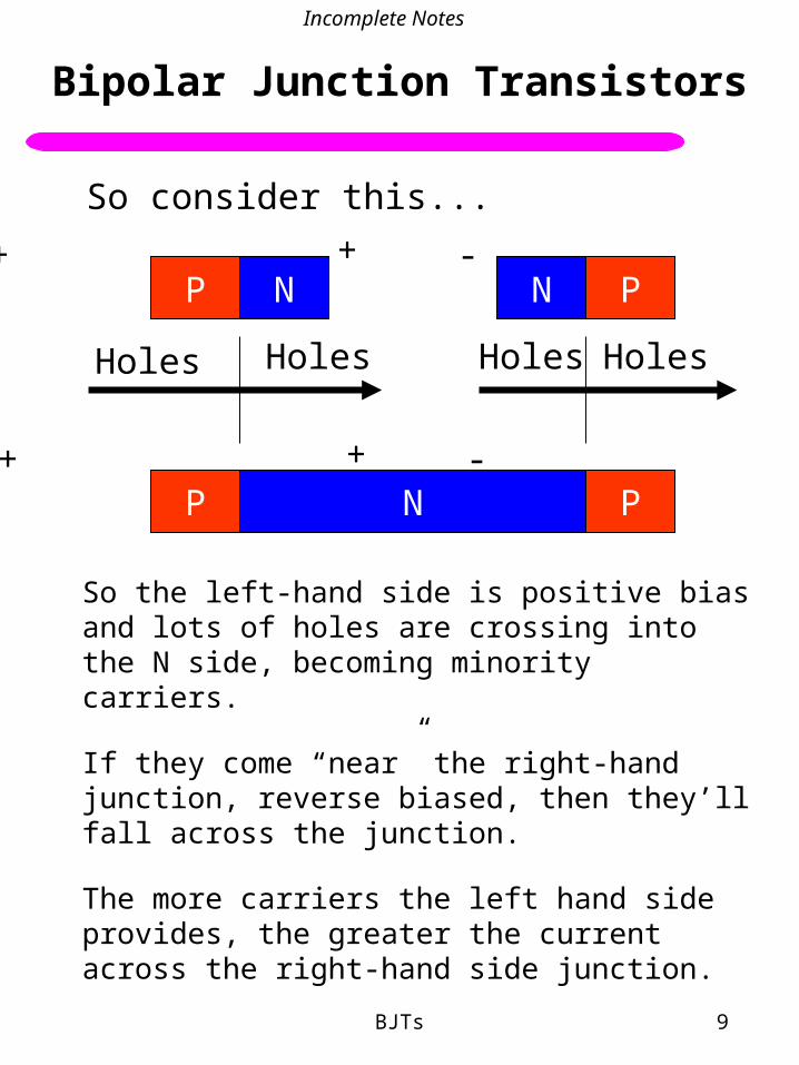
So consider this...
Bipolar Junction Transistors
P NN P
Holes Holes Holes Holes
So the left-hand side is positive bias and lots of holes are crossing into the N side, becoming minority carriers.
If they come “near” the right-hand junction, reverse biased, then they’ll fall across the junction.
The more carriers the left hand side provides, the greater the current across the right-hand side junction.
P N P
+ - + -
+ - + -

BJTs 10
Incomplete Notes
Now all is well and good with this idea, the principle of adding additional minority carriers into a substance is called carrier injection and the forward biased device is a minority carrier injection, or in or case a “hole injection device” (because we drew a PNP device).
Two questions need to be asked to make this a practical device
• Will all the injected holes get to the reverse biased junction?
• Will the forward biased junction actually work as we’ve drawn it?
Bipolar Junction Transistors

BJTs 11
Incomplete Notes
Now minority carriers in a material, outside of the depletion region, quickly meet a majority carrier and recombine, maintaining the long-term equilibrium.
However this takes some time, the lifetime of the minority carrier, , and this lifetime can be extended by making the doping of the material less.
Less dopant, therefore fewer majority carriers and hence a greater chance of a minority carrier lasting longer, thus the average lifetime of a minority carrier increases.
Bipolar Junction Transistors

BJTs 12
Incomplete Notes
But while the minority carrier is avoiding recombination it is also moving physically, with some speed (it physically crossed a barrier to become a minority carrier)
So as before, the speed of the carrier (electrons are faster than holes) and the average lifetime of the carrier gives us the average distance it will travel.
So if the width of the centre region is a small fraction of the average distance a carrier will travel then it is safe to say that the majority of the carriers will actually be caught by the pull of the electric field of the reverse biased junction and fall across the junction.
Bipolar Junction Transistors

BJTs 13
Incomplete Notes
So the other question was will it work as shown, well the answer is no.
No matter how dominant one current carrier is over the other, there is still some current contribution from the other type. So if P-type is massively dominant, the majority of the current will be carried by holes, but some, though a small amount, will be carried by electrons.
Also in the centre region, some recombination will occur, not all holes will get to the reverse biased junction (assuming a PNP device). Recombination removes a hole and an electron and these electrons have to be replenished from somewhere.
Bipolar Junction Transistors

BJTs 14
Incomplete Notes
Bipolar Junction Transistors
Another case where electrons play a role is that across even a reverse biased junction, there will be a current comprising of drift current. This will result in electrons entering into the base (assuming a PNP device).
This will provide some of the electrons needed to replenished the electrons removed by recombination, but it will be a very small portion of the number required.
The first two mechanisms far outweigh the third and ensure that a source of electrons for the base (assuming a PNP device) is required. Thus we need a base current to inject electrons.
BJTs 15
Incomplete Notes
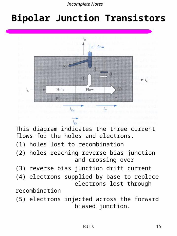
Bipolar Junction Transistors
This diagram indicates the three current flows for the holes and electrons.
(1) holes lost to recombination
(2) holes reaching reverse bias junction and crossing over
(3) reverse bias junction drift current
(4) electrons supplied by base to replace electrons lost through recombination
(5) electrons injected across the forward biased junction.

BJTs 16
Incomplete Notes
Collector-Emitter Current Ratio
Now these currents can be related by simple equations
)( pEC BII
In this equation B is called the Base Transport Factor, not to be confused with . The proportion of holes that leave the emitter and get to the reverse bias junction.
The ratio of the emitter current which is due to holes (assuming a PNP device) as a fraction of the total emitter current is called the emitter injection efficiency
E
pE
nEpE
pE
I
I
II
I )(
)()(
)(
Ideally, we’d like both of these to be as close to 1 as possible but both will be slightly less than one.

BJTs 17
Incomplete Notes
Collector-Emitter Current Ratio
E
E
pEC
I
IB
BII
)(
In this equation is called the current transfer ratio, and ideally we wish this to be as close to one as possible.
Now taking these two, B and we can come up with a relationship for IE and IC

BJTs 18
Incomplete Notes
Base-Collector Current Ratio
)()()( nCnrecombnEB IIII
Reverse biased junction drift current (very small, neglect)
The base current is to be found by investigating the current required to keep supplying electrons (assuming a PNP device) to the base to replace the net loss in electrons due to recombination, reverse bias junction drift and forward bias diffusion.
The current required to replenish the electrons lost through hole recombination.
The current component of the forward biased PN junction (emitter base) that is carried by electrons from the base to the emitter.

BJTs 19
Incomplete Notes
Base-Collector Current Ratio
BI
BI
BII
BII
IIII
pE
pE
pEpE
pEnE
nCnrecombnEB
1
11
11
1
)(
)(
)()(
)()(
)()()(
So looking at this more closely
BJTs 20
Incomplete Notes
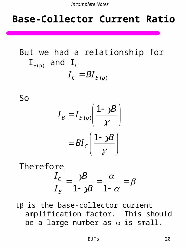
Base-Collector Current Ratio
But we had a relationship for IE(p) and IC
BBI
BII
C
pEB
1
1)(
)( pEC BII
So
11 B
B
I
I
B
C
is the base-collector current amplification factor. This should be a large number as is small.
Therefore

BJTs 21
Incomplete Notes
Quantitative Analysis of BJT
What we shall be doing in this section is investigating the behaviour of the system so as to be able to quantify the values of and . Throughout this analysis we shall be assuming a PNP device.
First we’ll make some simplifying assumptions:• The current across the forward biased junction is purely diffusion, there is no drift current component.
• The emitter current is purely composed of holes. (IE(n)=0, =1)
• The base collector reverse biased junction current is neglible and can be ignored.• The cross-sectional area of the device is constant.• All currents and voltages are stable and constant.

BJTs 22
Incomplete Notes
Quantitative Analysis of BJT
The key is to find the current that flows from the emitter to the collector. The difference is the base current. The current in a PN junction is based on the number of excess carriers in the base.. The excess hole concentration at the edge of a depletion region on the N side of a PN junction can be easily found from the diode equations.
1 kTqVn
junctionepp
pn is equilibrium number of holes

BJTs 23
Incomplete Notes
Quantitative Analysis of BJT
The excess carriers in the base at the edge of the depletion regions caused by the collector and emitter regions
1 kTqVnE
EBepp
1 kTqVnC
CBepp
Assuming emitter and collectorregions equally doped.
CB is a reverse biased voltage.

BJTs 24
Incomplete Notes
Quantitative Analysis of BJT
These can be simplified by assuming that VEB is much greater than 0.026V and that VCB is much less than -0.026V.
nC
kTqVnE
pp
epp EB
Using the diffusion equation we can work out the excess hole concentration as a factor of distance away from the junction, into the base, p(x).
Let xn be the variable and it represents distance in the base from the edge of the EB depletion region.
The effective width of the base, from depletion region edge to depletion region edge is WB

BJTs 25
Incomplete Notes
Quantitative Analysis of BJT
So using the diffusion equation,
22
2 )()(
P
n
n
n
L
xp
dx
xpd
Diffusion length fora hole
The solution for an equation of it type, in general is given by (it’s something you’d know or look up).
pnpn LxLxn eCeCxp 21)(
You’d solve this by looking at boundary conditions, in this case at xn=0 and xn=WB
CLWLW
bn
En
peCeCWxp
pCCxpPBPB
21
21
)(
)0(
BJTs 26
Incomplete Notes
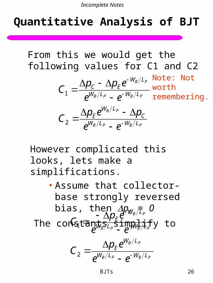
Quantitative Analysis of BJT
From this we would get the following values for C1 and C2
PBPB
PB
PBPB
PB
LWLWC
LWE
LWLW
LWEC
ee
pepC
ee
eppC
2
1
Note: Notworth remembering.
However complicated this looks, lets make a simplifications.
• Assume that collector-base strongly reversed bias, then pC = 0
The constants simplify to
PBPB
PB
PBPB
PB
LWLW
LWE
LWLW
LWE
ee
epC
ee
epC
2
1
BJTs 27
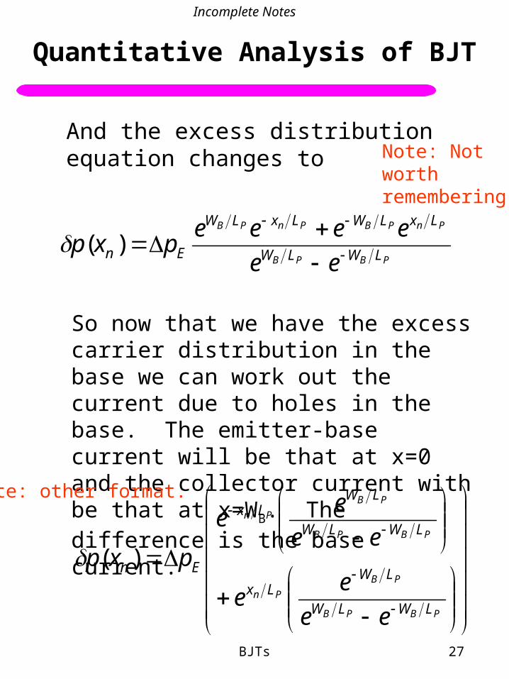
Incomplete Notes
Quantitative Analysis of BJT
And the excess distribution equation changes to Note: Not
worth remembering.
So now that we have the excess carrier distribution in the base we can work out the current due to holes in the base. The emitter-base current will be that at x=0 and the collector current with be that at x=WB. The difference is the base current.
PBPB
PnPBPnPB
LWLW
LxLWLxLW
En ee
eeeepxp
)(
PBPB
PB
Pn
PBPB
PB
Pn
LWLW
LWLx
LWLW
LWLx
En
ee
ee
ee
ee
pxp )(
Note: other format.

BJTs 28
Incomplete Notes
Quantitative Analysis of BJT
The current in the base due to holes is given by
So quickly looking at what the differential of the excess carriers is with respect to xn
n
npnP dx
xpdqADxI
)()(
P
n
LWLW
LWLx
LWLW
LWLx
Enn
n
L
xp
ee
ee
ee
ee
pdx
d
dx
xpd
PBPB
PB
Pn
PBPB
PB
Pn
)(
)(

BJTs 29
Incomplete Notes
Quantitative Analysis of BJT
So back to the current equation.
The current at the emitter edge of the base is when xn=0
n
npnP dx
xpdqADxI
)()(
21
)()0(
CCL
DqA
xpL
DqAxI
p
p
np
pnEp
The current at the collector edge of the base is when xn=0
PBPB LWLW
p
pBnC eCeC
L
DqAWxI 21)(

BJTs 30
Incomplete Notes
Quantitative Analysis of BJT
If we substitute the values of C1 and C2, we get expressions that are best described in hyperbolic functions.
p
BC
p
BE
p
pC
p
BC
p
BE
p
pE
L
Wctnhp
L
Whp
L
DqAI
L
Whp
L
Wctnhp
L
DqAI
csc
csc
Again not something really worth worrying about in detail, just understanding what we are trying to do is more important.
co-tan-hco-sec-h

BJTs 31
Incomplete Notes
Quantitative Analysis of BJT
So with IC and IE all we need to do now is subtract IC from IE and we’ll get the number of holes that recombined, and hence IB
p
BCE
p
pB
p
B
p
BCE
p
p
CEB
L
Wpp
L
DqAI
L
Wh
L
Wctnhpp
L
DqA
III
2tanh
csc
This formula for IB however is more interesting as it gives us a formula in terms of parameters we actually have.

BJTs 32
Incomplete Notes
Quantitative Analysis of BJT
If we make an assumption that the reverse bias junction is very reverse bias (as we have already assumed elsewhere) then we could say that the minority hole concentration close to the junction on the N side is pretty close to zero, ie
0 Cp
Hence we can get the following simplifications.
p
BE
p
pB
p
BE
p
pC
p
BE
p
pE
L
Wp
L
DqAI
L
Whp
L
DqAI
L
Wctnhp
L
DqAI
2tanh
csc
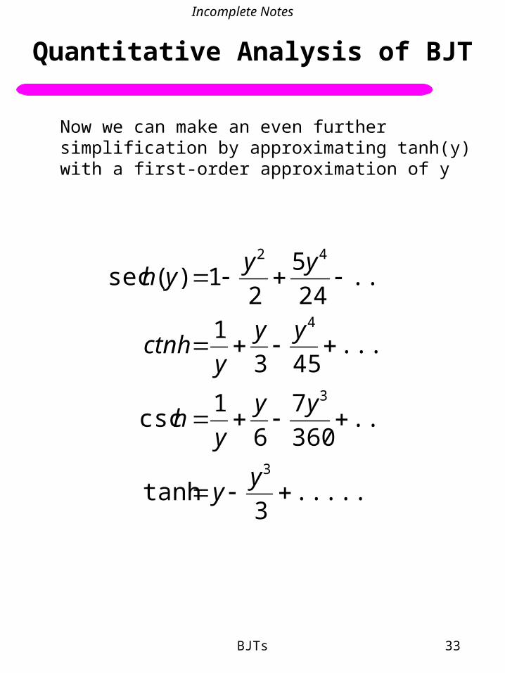
BJTs 33
Incomplete Notes
Quantitative Analysis of BJT
Now we can make an even further simplification by approximating tanh(y) with a first-order approximation of y
.....3
tanh
.....360
7
6
1csc
.....453
1
.....24
5
21)(sec
3
3
4
42
yy
yy
yh
yy
yctnh
yyyh

BJTs 34
Incomplete Notes
Quantitative Analysis of BJT
So working on that basis, we get
p
EBB
EB
p
p
p
EB
p
p
p
BE
p
pB
pWqAI
pW
L
DqA
L
pW
L
DqA
L
Wp
L
DqAI
2
2
2
2tanh
2
This accounts for hole recombination current but not the current injected back from the base to the emitter across the forward biased PN junction. However this can be kept small and neglected.

BJTs 35
Incomplete Notes
Quantitative Analysis of BJT
p
EBB
pWqAI
2
We can see from this that the base current, which we want to be small as it reduces and , is inversely proportional to p. So if we can increase p we could decrease IB and corresponding increase
p is the time between a hole finding an electron, so if there are less free electrons then p will go up. Thus reducing the doping in the N-type material increases p and reduces IB.
Making the N in the middle of the sandwich very lightly doped reduces recombination and improves the transistor performance.

BJTs 36
Incomplete Notes
Quantitative Analysis of BJT
p
EBB
pWqAI
2
A term which we’ll be investigating further is WB, the effective width of the base, ignoring the depletion regions. Increasing the length increases IB as it clearly would increase the recombination rate. Normally the base is made very narrow compared to the diffusion length, LP, to keep the recombination rate and thus IB low.
Another important parameter is A. Modifying the area of the junctions will decrease the base current. In practice the cross-sectional area of the channel is different across the device so as to optimise performance.

BJTs 37
Incomplete Notes
Quantitative Analysis of BJT
To get and , we need just to divide the two relevant currents.
Now these equations were defined for the normal operational mode of the transistor but they are cumbersome and where a range of assumptions have been made that are not true in real devices.
This analysis is important in that we can see how different parameters can effect the overall performance of the system, in particular, , the carrier lifetime.
B
C
I
I
E
C
I
I

BJTs 38
Incomplete Notes
Coupled Diode Equations (Ebers Moll)
This all works fine assuming that the collector junction is reversed biased. However this does not have to be the case though it is the normal mode of operation.
When it is not the case, we cannot discount the excess hole concentration pc in the base if this junction is forward biased.
If this is the case then we need to consider more generalised expressions for the currents across the junctions.
This approach uses the idea of coupled diodes and was first used by J.J. Ebers and J.L. Moll.

BJTs 39
Incomplete Notes
Coupled Diode Equations (Ebers Moll)
Consider in general that the current flowing across each junction can be split into a superposition of currents. As before we only need consider the hole current as it’s a PNP device.
We call the currents in the expected directions, normal currents.
IEN: the current from emitter to base.
ICN: the current from base to collector.
On a similar basis, current components flowing in the opposite direction are called inverted currents.
IEI: the current from base to emitter.
ICI: the current from collector to base.

BJTs 40
Incomplete Notes
Coupled Diode Equations (Ebers Moll)
These current components can be found from:
p
BC
p
BE
p
pC
p
BC
p
BE
p
pE
L
Wctnhp
L
Whp
L
DqAI
L
Whp
L
Wctnhp
L
DqAI
csc
csc
providing that the cross-sectional area of the device is constant.
Let us also assume that the doping in the collector and the emitter is the same.

BJTs 41
Incomplete Notes
Coupled Diode Equations (Ebers Moll)
From these equations we can define some constants:
Using these, the current components can now be expressed as
Minus sign because they are flowing in the opposite direction to our expected current flows
p
B
p
p
p
B
p
p
L
Wh
L
DqAb
L
Wctnh
L
DqAa
csc

BJTs 42
Incomplete Notes
Coupled Diode Equations (Ebers Moll)
Combining the different current components.
Looking at IE a little more closely, we get that

BJTs 43
Incomplete Notes
Coupled Diode Equations (Ebers Moll)
Similarly we can express IC in a similar form.
Now these equations are perfectly fine for symmetric devices (constant area, equal doping) but to factor in asymmetric devices.
Consider IC when pE=0,
This would be the collector current when VEB=0. ICS would be a number representing the collector current at that time. Similarly for IE
BJTs 44
Incomplete Notes
Coupled Diode Equations (Ebers Moll)
Now if we define a new term for the proportion of each current contribution that gets across to the other region, ie the number of carriers from the emitter to the collector, and visa-versa.
BJTs 45
Incomplete Notes
Coupled Diode Equations (Ebers Moll)
Finally adding all these together

BJTs 46
Incomplete Notes
Coupled Diode Equations (Ebers Moll)
11
11
kTqVCS
kTqVESNC
kTqVCSI
kTqVESE
CBEB
CBEB
eIeII
eIeII
These are the basic Eber Moll equations and are valid for all configurations and bias voltages.
It defines the collector and emitter currents in terms of only four parameters which could be measured.
N, I, IES and ICS
It can be shown, but we won’t prove it, that

BJTs 47
Incomplete Notes
Coupled Diode Equations (Ebers Moll)
It is possible to simplify the equations by noting that IEN and ICI are defined by diode equations. This is why they are called the coupled-diode equations. If we use the relationship
we can get
similarly
The Ebers Moll Equations are often expressed in this form as it leads to an easy circuit representation of the result.

BJTs 48
Incomplete Notes
Coupled Diode Equations (Ebers Moll)
1
1
kTqV
COENC
kTqVEOCIE
CB
EB
eIII
eIII
This has a circuit representation as
E C
B
EN I
CI I 1kTqVCO
CBeI
1kTqVEO
EBeI
IE
ICIB
This model is the basis of all the expanded models used in computer SPICE simulations.

BJTs 49
Incomplete Notes
Non-Idealities - Base Narrowing
Now in all our discussions so far we made an assumption that recombination of holes in the base region was small (assuming a PNP device). This could be ensured by
• lightly doping the base so that there are less free electrons and hence less chance of recombination• Keeping the width of the base small compared to the diffusion length.
An effect of the light doping is that if the emitter or the collector are heavily doped (which they normally are) then most of the depletion region will be within the base.

BJTs 50
Incomplete Notes
Non-Idealities - Base Narrowing
Now the width of the depletion region of the reverse biased collector junction is going to be mainly in the base.
As the base is lightly doped it may extend quite a significant degree into the base.
The width of the region will vary according to the collector voltage, ie it will vary with VCE.
But it needs to be remembered that the length of the base is an important factor in determining the number of holes that recombine. The smaller the distance, the less holes.

BJTs 51
Incomplete Notes
Non-Idealities - Base Narrowing
The less recombination, the more efficient the transistor, goes up, more collector current flows for the same base current.
So simply, as VCE increases, for the same base current, the collector current increases.
Thus in saturation we have a slope to the curves, and this is nearly a linear relationship. If these linear curves were extrapolated back they would intersect at the same point on the IC=0 axis, at a point which we called -VA, where VA is the Early Voltage

BJTs 52
Incomplete Notes
Non-Idealities - Base Narrowing

BJTs 53
Incomplete Notes
Non-Idealities - Base Narrowing
If the depletion region were to grow such that it filled the base, then we’d have a phenomenon called Punch-through.
All emitter holes would be collected in the collector. There would be no recombination and hence no transistor effect.
This normally doesn’t occur in practice as avalanche failure normally occurs first.
It can be avoided by minimising the base-collector reverse bias voltage.

BJTs 54
Incomplete Notes
Non-Idealities - Avalanche Failure
This occurs when the voltage across the reverse bias junction is so great that avalanche failure commences.
This produces additional current that feeds into the circuit.
The common-emitter configuration is more prone to avalanche failure than common base

BJTs 55
Incomplete Notes
Non-Idealities - Thermal Runaway
In BJT’s the parameters can vary with temperature. In particular can vary substantially.
In silicon or germanium, the lifetime of an excess carrier, , increases with temperature. However mobility decreases by approximately T-3/2. However the net effect is normally that the increased lifetime dominates and increases.
If increases then for the same IB the collector current increases.

BJTs 56
Incomplete Notes
Non-Idealities - Thermal Runaway
So consider this case. The transistor has been biased such that it has a large IC. This current by the voltage dropped across VCE determines the power dissipated in the BJT transistor.
Power equals heat, if the heat cannot dissipate quickly enough then the silicon warms up.
The silicon warms up, increases, so the collector current increases. This means that more power is produced and hence more heat. This increases until so much heat is produced that the device fails. Graphically.. It smokes…
This is a BJT effect and has to be designed against in the circuit using the BJT. Emitter degenerated Common Emitter circuits are immune to this.

BJTs 57
Incomplete Notes
Large Signal Parasitics
Before we look at small signal, there are some large signal non-idealities that should be considered.
Any current flowing through a piece of semiconductor experiences a resistance.
Any PN junction also includes a capacitor. So what we will do on the next page is indicate where these parasitics are.
N EmitterP BaseN Collector

BJTs 58
Incomplete Notes
Large Signal Parasitics
N EmitterP BaseN Collector
E
B
C
Rb
CjC
CjE
RC
RE
Parasitic junction capacitances.
Less and smaller parasitics than in MOSFETs.

BJTs 59
Incomplete Notes
Small Signal Model
The small signal models of the BJT that are most commonly used are the hybrid or the H-parameter models. These are very similar to each other. The simplified ideal H-parameter model is shown below.
N EmitterP BaseN Collector
+vBE
-
+vCE
-
iB iC
hi hohf iB
B
E
C

BJTs 60
Incomplete Notes
Small Signal Model
rin/hie the “equivalent” resistance across the forward biased junction and also the base and emitter bulk resistances. Very low.
ho/ro the equivalent” resistance across the reverse biased junction and also the collector, base and emitter bulk resistances. Very high due to reverse bias junction.
hfe/ is a value that is heavily dependent on the emitter efficiency and the base transport factor. Ideally high.
N EmitterP BaseN Collector

BJTs 61
Incomplete Notes
Parasitics in the Small Signal Model
The main parasitics are the capacitors and the emitter resistance. The emitter resistance can be ignored as well in many analyses.
+vBE
-
+vCE
-
iB iC
hi hohf iB
B
E
C
N EmitterP BaseN Collector
Cje
Cjc

BJTs 62
Incomplete Notes
Example
Assuming that the PNP device is biased as per normal with an emitter base voltage of +1 Volt, calculate the current transport factor, , and the current gain term, Calculate the change in for an emitter base voltage of +2 Volt. Assume the Base transport factor B is ideal and equal to one.
Device cross-sectional Area = 10-4 /cm2
Effective width of base region = 10-4 cm
ni2 = 2.1020 /cm3
cm/s6800cm/s3800 N
N
P
P
L
D
L
D
316318 dopants/cm10dopants/cm10 DA NN

BJTs 63
Incomplete Notes
Example

BJTs 64
Incomplete Notes
Example

BJTs 65
Incomplete Notes
Example

BJTs 66
Incomplete Notes
Example

BJTs 67
Incomplete Notes
Example
Explain the process of base narrowing. Assuming that the forward bias region has a negligible depletion region within the base, determine the voltage at which punch-through occurs in the following NPN device at 125 degC (a hot but still functioning transistor).
Device cross-sectional Area = 10-4 /cm2
Width of base region = 10-3 cm
ni2 = 2.1020 /cm3
cm/s6800cm/s3800 N
N
P
P
L
D
L
D
318314 dopants/cm10dopants/cm10 DA NN
KTmVq
kTdeg400@35

BJTs 68
Incomplete Notes
Example

BJTs 69
Incomplete Notes
Example