Implementation of WCDMA Correlation Pool in Dynamically...
85
Implementation of WCDMA Multi-Finger Correlation Pool in Dynamically Reconfigurable Resource Array GUO CHEN Master’s Degree Project Stockholm, Sweden 2011 TRITA-ICT-EX-2011:294
Transcript of Implementation of WCDMA Correlation Pool in Dynamically...

Implementation of WCDMA Multi-FingerCorrelation Pool in Dynamically
Reconfigurable Resource Array
GUO CHEN
Master’s Degree ProjectStockholm, Sweden 2011
TRITA-ICT-EX-2011:294


Acknowledgements
I would like to thank my parents and Sisi Mao, for their great support formy study in Royal Institute of Technology (KTH).
I appreciate my examiner Professor Ahmed Hemani for this great opportu-nity of master thesis and his stringent requirement of the project. Specialthanks to my supervisor PhD candidate Shuo Li, for his patient and carefulguidance and inspiration throughout the project.
I would also like to thank all the members from DRRA group, for theirgenerously sharing of experience and encouragement which helped me maketremendous progress.

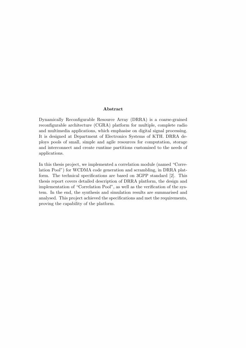
Abstract
Dynamically Reconfigurable Resource Array (DRRA) is a coarse-grainedreconfigurable architecture (CGRA) platform for multiple, complete radioand multimedia applications, which emphasise on digital signal processing.It is designed at Department of Electronics Systems of KTH. DRRA de-ploys pools of small, simple and agile resources for computation, storageand interconnect and create runtime partitions customised to the needs ofapplications.
In this thesis project, we implemented a correlation module (named “Corre-lation Pool”) for WCDMA code generation and scrambling, in DRRA plat-form. The technical specifications are based on 3GPP standard [2]. Thisthesis report covers detailed description of DRRA platform, the design andimplementation of “Correlation Pool”, as well as the verification of the sys-tem. In the end, the synthesis and simulation results are summarised andanalysed. This project achieved the specifications and met the requirements,proving the capability of the platform.


Contents
1 Multi-Finger Correlation Pool in WCDMA 1
1.1 Introduction to WCDMA . . . . . . . . . . . . . . . . . . . . 1
1.1.1 Code Division Multiple Access . . . . . . . . . . . . . 1
1.1.2 Wideband Code Division Multiple Access . . . . . . . 1
1.2 Spreading and Despreading in WCDMA . . . . . . . . . . . . 2
1.3 RAKE Receiver . . . . . . . . . . . . . . . . . . . . . . . . . . 3
1.3.1 Multipath Fading . . . . . . . . . . . . . . . . . . . . . 3
1.3.2 RAKE Receiver . . . . . . . . . . . . . . . . . . . . . . 4
1.4 Multi-Finger Correlation Pool . . . . . . . . . . . . . . . . . . 5
1.4.1 Channelisation Codes . . . . . . . . . . . . . . . . . . 6
1.4.2 Scrambling Codes . . . . . . . . . . . . . . . . . . . . 7
1.5 Summary . . . . . . . . . . . . . . . . . . . . . . . . . . . . . 8
2 Dynamically Reconfigurable Resource Array 9
2.1 Introduction . . . . . . . . . . . . . . . . . . . . . . . . . . . . 9
2.2 DRRA Architecture . . . . . . . . . . . . . . . . . . . . . . . 10
2.2.1 Morphable Datapath Unit . . . . . . . . . . . . . . . . 10
2.2.2 Register File . . . . . . . . . . . . . . . . . . . . . . . 11
2.2.3 Switchbox . . . . . . . . . . . . . . . . . . . . . . . . . 12
2.2.4 SRAM Memory . . . . . . . . . . . . . . . . . . . . . . 13
2.2.5 Control Logic . . . . . . . . . . . . . . . . . . . . . . . 13
2.3 DRRA Design Flow . . . . . . . . . . . . . . . . . . . . . . . 14
2.4 CDMA Modes of mDPU . . . . . . . . . . . . . . . . . . . . . 14
2.4.1 Code Generation Mode . . . . . . . . . . . . . . . . . 16
2.4.2 Vector Rotation Mode . . . . . . . . . . . . . . . . . . 17
2.4.3 Other Modes . . . . . . . . . . . . . . . . . . . . . . . 18
2.5 Summary . . . . . . . . . . . . . . . . . . . . . . . . . . . . . 18
3 Correlation Pool in DRRA 19
3.1 Multi-Finger Correlation Pool Specifications . . . . . . . . . . 19
3.2 Hardware Allocation in DRRA . . . . . . . . . . . . . . . . . 20
3.3 Sequencer Instructions . . . . . . . . . . . . . . . . . . . . . . 22
3.4 Algorithm and Implementation . . . . . . . . . . . . . . . . . 24
i

3.4.1 Stimuli and Controller . . . . . . . . . . . . . . . . . . 243.4.2 Code Generator . . . . . . . . . . . . . . . . . . . . . . 263.4.3 Complex Multiplier-Accumulator . . . . . . . . . . . . 27
3.5 Timing Graph of Control and Communication . . . . . . . . . 283.6 Summary . . . . . . . . . . . . . . . . . . . . . . . . . . . . . 30
4 System Verification 314.1 Project Directory Structure . . . . . . . . . . . . . . . . . . . 314.2 The MANAS Tool . . . . . . . . . . . . . . . . . . . . . . . . 32
4.2.1 MANAS Directory Structure . . . . . . . . . . . . . . 324.2.2 Using MANAS . . . . . . . . . . . . . . . . . . . . . . 334.2.3 Testbench Structure . . . . . . . . . . . . . . . . . . . 33
4.3 Synthesis Results . . . . . . . . . . . . . . . . . . . . . . . . . 344.3.1 Technology . . . . . . . . . . . . . . . . . . . . . . . . 344.3.2 Critical Path . . . . . . . . . . . . . . . . . . . . . . . 344.3.3 Gate Count . . . . . . . . . . . . . . . . . . . . . . . . 344.3.4 Power Consumption Estimation . . . . . . . . . . . . . 34
4.4 Functional Verification Methodology . . . . . . . . . . . . . . 354.4.1 Verification Flow . . . . . . . . . . . . . . . . . . . . . 354.4.2 Reconfiguration . . . . . . . . . . . . . . . . . . . . . . 37
4.5 Verification Environment . . . . . . . . . . . . . . . . . . . . 384.6 Verification Results . . . . . . . . . . . . . . . . . . . . . . . . 384.7 Performance and Capacity Verification . . . . . . . . . . . . . 424.8 Summary . . . . . . . . . . . . . . . . . . . . . . . . . . . . . 42
5 Conclusion and Future Work 43
A Sequencer Instructions I
B mDPU Modes XV
C Configwares for Correlation Pool Algorithm XVIIC.1 Definitions of Global Constants . . . . . . . . . . . . . . . . . XVIIC.2 Configware for Controller . . . . . . . . . . . . . . . . . . . . XIXC.3 Configware for Stimuli . . . . . . . . . . . . . . . . . . . . . . XXIC.4 Configware for Worker (MAC) . . . . . . . . . . . . . . . . . XXIIIC.5 Configware for Worker (Code Generator) . . . . . . . . . . . XXIV
ii

List of Figures
1.1 Spreading and despreading in DS-CDMA . . . . . . . . . . . 21.2 Spread signal in spectrum view . . . . . . . . . . . . . . . . . 31.3 Comparison of Despreading with own and other data . . . . . 41.4 Block diagram of a RAKE receiver . . . . . . . . . . . . . . . 51.5 Block diagram of multi-finger correlation pool . . . . . . . . . 51.6 OVSF Code Generation Tree . . . . . . . . . . . . . . . . . . 61.7 Scrambling sequence generator . . . . . . . . . . . . . . . . . 7
2.1 DRRA Physical Layer Fabric Architecture . . . . . . . . . . . 112.2 Reachable DRRA Cells in 3-Hop Local Connectivity Area . . 122.3 DRRA Design Flow . . . . . . . . . . . . . . . . . . . . . . . 152.4 Serial OVSF Code Generator . . . . . . . . . . . . . . . . . . 162.5 Format of the Output Correlation Codes . . . . . . . . . . . . 172.6 Format of the Input Complex Samples . . . . . . . . . . . . . 17
3.1 Correlation Pool Diagram . . . . . . . . . . . . . . . . . . . . 203.2 Allocation of DRRA Cells for One Worker . . . . . . . . . . . 203.3 Allocation of DRRA Cells in DRRA Fabric . . . . . . . . . . 213.4 Numbering Rules for Sequencers . . . . . . . . . . . . . . . . 223.5 Flowcharts of Stimuli and Controller . . . . . . . . . . . . . . 253.6 Flowchart of Code Generator . . . . . . . . . . . . . . . . . . 263.7 Flowchart of Complex MAC . . . . . . . . . . . . . . . . . . . 283.8 Timing Graph of Correlation Pool . . . . . . . . . . . . . . . 29
4.1 Directory Structure of Correlation Pool Project . . . . . . . . 314.2 Testbench Structure . . . . . . . . . . . . . . . . . . . . . . . 334.3 Correlation Pool Verification Flow . . . . . . . . . . . . . . . 35
iii


List of Tables
2.1 Complex Multiplication Results . . . . . . . . . . . . . . . . . 18
4.1 Reconfiguration of Global Constants for Different SFs . . . . 37
5.2 Comparison of Specifications and Synthesis Results . . . . . . 43
iv


List of Abbreviations
3GPP 3rd Generation Partnership Project
AGU Address Generation Unit
CCPCH Common Control Physical CHannel
CGRA Coarse Grained Reconfigurable Architecture
CPICH Common Pilot CHannel
DRRA Dynamically Reconfigurable Resource Array
MANAS MANual ASsembly
mDPU Morphable Datapath Unit
OVSF Orthogonal Variable Spreading Factor
SF Spreading Factor
SoC System-on-chip
VCD Value Change Dump
WCDMA Wideband Code Division Multiple Access
v


Chapter 1
Multi-Finger CorrelationPool in WCDMA
1.1 Introduction to WCDMA
1.1.1 Code Division Multiple Access
CDMA is a channel access method in radio communication context. It isbased on spread-spectrum technology and with unique code sequences(pseudo-noise-like sequences) for each user to allow multiple users to utilise the samecarrier frequency simultaneously.
In CDMA system the bandwidth is much higher than data rate, resultingthe transmission power is spread over the wide range of spectrum. There area few common spectrum spreading techniques, for example, Direct-SequenceSpread Spectrum (DSSS, which is used in WCDMA system), Frequency-Hopping Spread Spectrum (FHSS), Chirp Spread Spectrum (CSS), andTime-Hopping Spread Spectrum (THSS).
1.1.2 Wideband Code Division Multiple Access
WCDMA is an air interface standard in 3G mobile telecommunication net-works. The transmission technique used in WCDMA is Direct-SequenceCDMA (DS-CDMA). The WCDMA system utilises 5 MHz radio channelwidth, and its chip rate is 3.84 MHz. There are two operating modes in thephysical layer of WCDMA, respectively, Frequency-Division Duplex (FDD)mode and Time-Division Duplex (TDD) mode. As their names suggest, inFDD mode, different frequencies are used for uplink and downlink; whilein TDD mode, the carrier frequency is shared between uplink and down-link. Comparing to FDD mode, TDD mode requires more synchronisationscheduling between uplink and downlink. In this thesis project, we onlyconcern the physical layer of WCDMA in FDD mode.

2 Section 1.2
1.2 Spreading and Despreading in WCDMA
By using the spectrum spreading technique, WCDMA provides secured com-munications, which are highly resistant to interference and jamming.
1
-1
1 1
-1
+1
-1
+1
-1
+1
-1
+1
-1
+1
-1
1
-1
1 1
-1
Symbol
Chip
Original Data
Spreading
Code
Spread signal
= Data x Code
Spreading
Code
Expected Data
= Spread signal x Code
Spreading
t
t
t
t
t
Despreading
Figure 1.1: Spreading and despreading in DS-CDMA
Figure 1.1 illustrates the basic concept of spreading and despreadingtechniques in a basic DS-CDMA system.
In the spreading phase, user data is chip-wisely multiplied by the spread-ing code (a pseudo-random sequence, which is mutually orthogonal to anyother spreading code). The resulting signal rate is the chip rate, which is theoriginal symbol rate increased by a factor of SF (SF, Spreading Factor =Chip rate
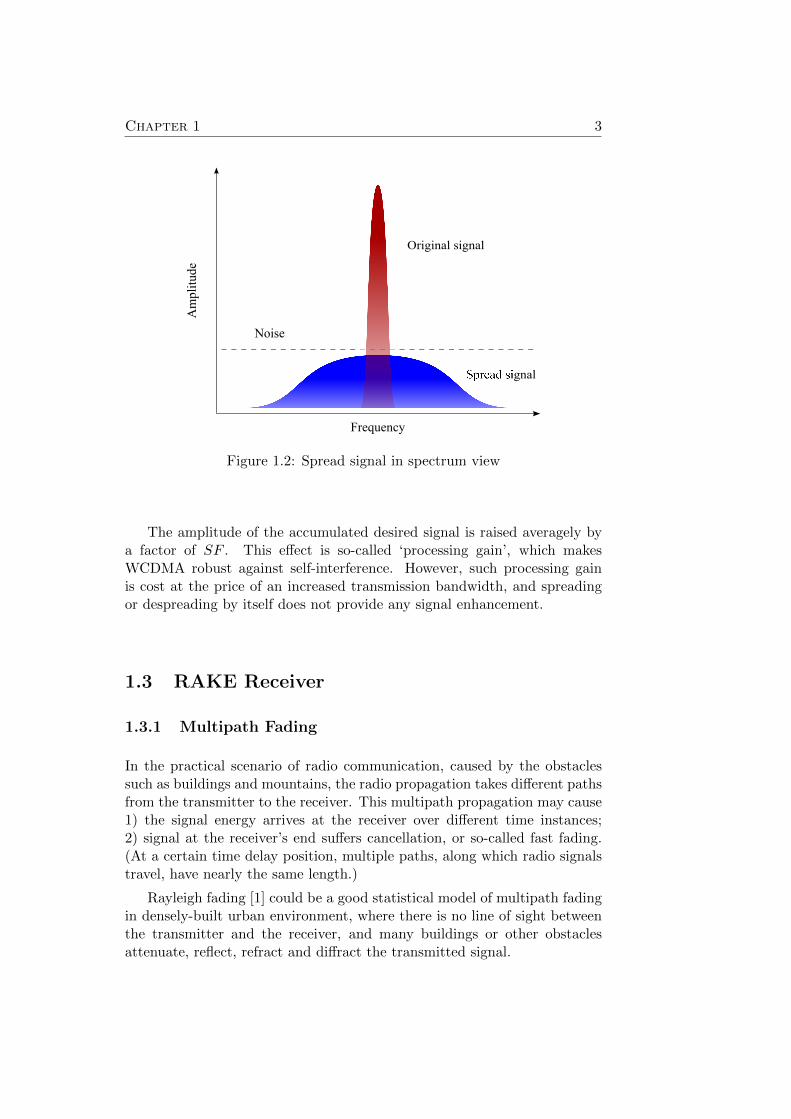
Symbol rate). After spreading, the original user data is spread over widerfrequency spectrum, resulting lower amplitude. By scrambling the spreadsignal, the energy density over the whole spectrum is then normalised. Thisis demonstrated in Figure 1.2.
In the despreading phase as Figure 1.1 depicts, the spread signal is mul-tiplied by the same spreading code at the receiver’s end. With the perfectsynchronised code, the original user data could be recovered, as shown inFigure 1.1. The despreading procedure is achieved by the correlation re-ceiver in a WCDMA device.
In Figure 1.3, the signal from another user is received at the correlationreceiver. The accumulation result of this despread signal is averagely zero,since the spreading codes are orthogonal to each other. Only the desiredsignal results a reasonable amplitude for the hard decision-maker in thelater procedures.
Chapter 1 3
Original signal
Spread signal
Noise
Frequency
Am
pli
tude
Figure 1.2: Spread signal in spectrum view
The amplitude of the accumulated desired signal is raised averagely bya factor of SF . This effect is so-called ‘processing gain’, which makesWCDMA robust against self-interference. However, such processing gainis cost at the price of an increased transmission bandwidth, and spreadingor despreading by itself does not provide any signal enhancement.
1.3 RAKE Receiver
1.3.1 Multipath Fading
In the practical scenario of radio communication, caused by the obstaclessuch as buildings and mountains, the radio propagation takes different pathsfrom the transmitter to the receiver. This multipath propagation may cause1) the signal energy arrives at the receiver over different time instances;2) signal at the receiver’s end suffers cancellation, or so-called fast fading.(At a certain time delay position, multiple paths, along which radio signalstravel, have nearly the same length.)
Rayleigh fading [1] could be a good statistical model of multipath fadingin densely-built urban environment, where there is no line of sight betweenthe transmitter and the receiver, and many buildings or other obstaclesattenuate, reflect, refract and diffract the transmitted signal.

4 Section 1.3
+1
-1
+1
-1
+1
-1
1
-1
1 1
-1
Desired Signal
Spreading
Code
Data after Despreading
= Spread signal x Code
+8
-8
Data after Integration
+1
-1
Other Signal
(Data:10011;
Code:00111100)
+1
-1
Spreading
Code
+1
-1
Other Data after
Despreading
+8
-8
Data after Integration
t
t
t
t
t
t
t
t
Figure 1.3: Comparison of Despreading with own and other data
1.3.2 RAKE Receiver
Due to multipath propagation and probably also multiple receive antennas,it is necessary to recover the energy from all paths and/or antennas. Thus,multiple correlation receivers could be utilised. Such correlation receiver istermed as a ‘finger’. In a RAKE receiver, a collection of correlation receivers(fingers) is employed.
The basic block diagram of a RAKE receiver is shown in Figure 1.4. Thedigitised signal from the RF circuitry is sent to each finger in the form ofI (In-phase) and Q (Quadrature). The despreading and integration to userdata symbols are performed by code generators and the correlators. Thechannel estimator uses the pilot symbols for estimating the channel statewhich will then be removed by the phase rotator from the received symbols.Then the difference in the arrival times of the symbols will compensate indelay in each finger. The combiner, commonly known as Maximum RatioCombiner (MRC), sums the channel-compensated symbols to recover theenergy across all delay positions, thus providing multipath diversity againstfading. The match filter in the figure is used for determining and updating

Chapter 1 5
Figure 1.4: Block diagram of a RAKE receiver
the current multipath delay profile of the channel.In addition, multiple receive antennas can be accommodated in the same
way as multiple paths received from a single antenna: by adding additionalRAKE fingers to the antennas, all the energy from multiple paths and an-tennas then can be received. Thus, from the perspective of RAKE receiver,the effects of multipath and multiple receive antennas have no differences.
1.4 Multi-Finger Correlation Pool
In this project, we are implementing multi-finger correlation pool into Dy-namically Reconfigurable Resource Array (DRRA) [6]. As depicted in Figure1.4, the multi-finger correlation pool indicates the correlator and pseudo-random sequence generator in the form of multi-finger, which is shown inFigure 1.5.
Figure 1.5: Block diagram of multi-finger correlation pool

6 Section 1.4
1.4.1 Channelisation Codes
The channelisation codes are Orthogonal Variable Spreading Factor (OVSF),which can provide orthogonality between a user’s different physical channels.In the tree in Figure 1.6, we describe the channelisation codes as Cch,SF,k,where SF is the spreading factor while k is the code number, 0 ≤ k ≤ SF−1.Since in WCDMA-FDD, the chip rate is 3.84Mchip/s, SF has the range of4 ≤ 2n ≤ 256, resulting in a data rate from 15k symbols/s (30kbits/s) up to960k symbols/s (1.92Mkbits/s) for each physical channel.
C =(1)ch,1,0
C =(1,1)ch,2,0
C =(1,-1)ch,2,1
C =(1,1,1,1)ch,4,0
C =(1,-1,1,-1)ch,4,2
C =(1,1,-1,-1)ch,4,0
C =(1,-1,-1,1)ch,4,0
Figure 1.6: OVSF Code Generation Tree
The generation method is defined as follows:
Cch,1,0 = 1,(Cch,2,0
Cch,2,1
)=
(Cch,1,0 Cch,1,0
Cch,1,0 −Cch,1,0
)=
(1 11 −1
),
Cch,2(n+1),0
Cch,2(n+1),1
Cch,2(n+1),2
Cch,2(n+1),3
.
.Cch,2(n+1),2(n+1)−2
Cch,2(n+1),2(n+1)−1
=
Cch,2n,0 Cch,2n,0
Cch,2n,0 −Cch,2n,0
Cch,2n,1 Cch,2n,1
Cch,2n,1 −Cch,2n,1
. .
. .Cch,2n,2n−1 Cch,2n,2n−1
Cch,2n,2n−1 −Cch,2n,2n−1
.
The leftmost value in each channelisation code word corresponds to the chiptransmitted first in time. The channelisation code for the primary CPICH(common pilot channel) is fixed to Cch,256,0 and the channelisation code forthe primary CCPCH (common control physical channel) is fixed to Cch,256,1.The codes for all other physical channels are assigned by the Radio AccessNetwork.

Chapter 1 7
1.4.2 Scrambling Codes
The long scrambling sequences Clong1,n and Clong2,n are constructed fromposition-wise modulo 2 sum of 38400 chip segments of two binary m-sequencesgenerated by means of two generator polynomials of degree 25. Here we as-sume the two m-sequences are x and y. The x sequence is constructed usingthe primitive polynomial X25 +X3 +1. The y sequence is constructed usingX25 + X3 + X2 + X + 1. Thus the resulting sequences constitute segmentsof a set of Gold sequences. And the Clong2,n sequence is a 16777232 chipshifted version of the sequence Clong1,n.
Figure 1.7: Scrambling sequence generator
Let n23...n0 be the 24 bit binary representation of the scrambling se-quence number n with n0 as the LSB. The x sequence depends on the chosenscrambling sequence number n and is denoted xn in the sequel. xn(i) andy(i) represent the i:th symbol of the sequence xn and y.
The m-sequence xn and y are constructed as follows:Initial conditions:
xn0 = n0, xn(1) = n1, ... = xn(22) = n22, xn(23) = n23, xn(24) = 1. (1.1)
y(0) = y(1) = ... = y(23) = y(24) = 1. (1.2)
Recursive definition of subsequent symbols:
xn(i + 25) = xn(i + 3) + xn(i) mod 2, i = 0, ..., 225 − 27. (1.3)
y(i+25) = y(i+3)+y(i+2)+y(i+1)+y(i) mod 2, i = 0, ..., 225−27. (1.4)
Define the binary Gold sequence zn by:
zn(i) = xn(i) + y(i) mod 2, i = 0, 1, 2, ..., 225 − 2. (1.5)
The real valued Gold sequence Zn is defined by:
Zn(i) =
{+1 if zn(i) = 0−1 if zn(i) = 1
, i = 0, 1, ..., 225 − 2. (1.6)

8 Section 1.5
Then the real-valued long scrambling sequences clong1,n and clong2,n can bedefined as follows:
clong1,n(i) = Zn(i), i = 0, 1, 2, ..., 225 − 2 (1.7)
clong2,n(i) = Zn
((i + 16777232) mod (225 − 1)
), i = 0, 1, 2, ..., 225 − 2. (1.8)
Finally, the complex-valued long scrambling sequence Clong,n could be de-fined as:
Clong,n(i) = clong1,n(i)(1 + j(−1)iclong2,n(2bi/2c)
)(1.9)
where i = 0, 1, ..., 225 − 2 and b c means rounding to nearest lower integer.The block diagram can be depicted as Figure 1.7.
1.5 Summary
In this chapter we covered basic theory we will use in the implementationof correlation pool in DRRA. We firstly introduced how and why spreadingand despreading mechanisms work in WCDMA. Afterwards, we introducedthe principles of the Correlation Pool and its basic model. This chapter alsocovers the WCDMA-FDD specifications for the channelisation codes andscrambling codes from 3GPP [2].

Chapter 2
Dynamically ReconfigurableResource Array
2.1 Introduction
DRRA stands for Dynamically Reconfigurable Resource Array. It is acoarse-grained reconfigurable architecture platform for multiple, completeradio and multimedia applications, which emphasise on digital signal pro-cessing. There are three highlighted concepts of DRRA:
1. Minimised movement of data;
2. Reconfigurable and programmable architecture for reuse and differentapplications;
3. Tolerant to manufacturing variations and runtime failure of some re-sources.
The key principle behind DRRA is to deploy pools of small, simple andagile resources for computation, storage and interconnect and create run-time partitions customised to the needs of applications [3]. Partitions willbe created for different applications. The partition is both logically andphysically a cluster of resources. Once the data enters the chip, it remainsstationary in its memory position. This property of ‘Move Logic Not Data’eliminates the infrastructure overhead energy and performance inefficiencieswhich result from sharing computational, storage and interconnect resourcesand exchanging the data between different resources.
The DRRA architecture could be reconfigured and programmed easily.It is different from ASIC that the customisation of DRRA is at coarse grainarchitecture blocks level, while that of ASIC is at standard cell level [5]. Thedifference between FPGA is that it is domain-specific and coarse-grainedthat improves computation and reconfiguration efficiency. The DRRA couldbe programmed by using DRRA’s own function library. The function library
10 Section 2.2
is an abstract function consists of several function properties and templates.The programmer can use the pre-defined instructions to build a readableconfigware (Refer to Section 2.3) for each sequencer for specific purposes ofuse. By using the automatic code generator, the configware will be con-verted to the corresponding sequencer programme, which is used in DRRAfabric. The programmer needs only to provide configuration of the specificapplication, in terms of configware, while the generation of the sequencerprogramme is automatically done.
Manufacturing variations in deep sub-micron geometries might createa yield problem and also might have the probability of hardware failure.DRRA with its regular topology and its principle of pool of resources,can avoid this problem by isolating failed and out-of-range performanceresources. Furthermore, with its reconfigurable and programmable archi-tecture, DRRA can easily cope with changes of specifications by modifyinghigher level software programmes.
2.2 DRRA Architecture
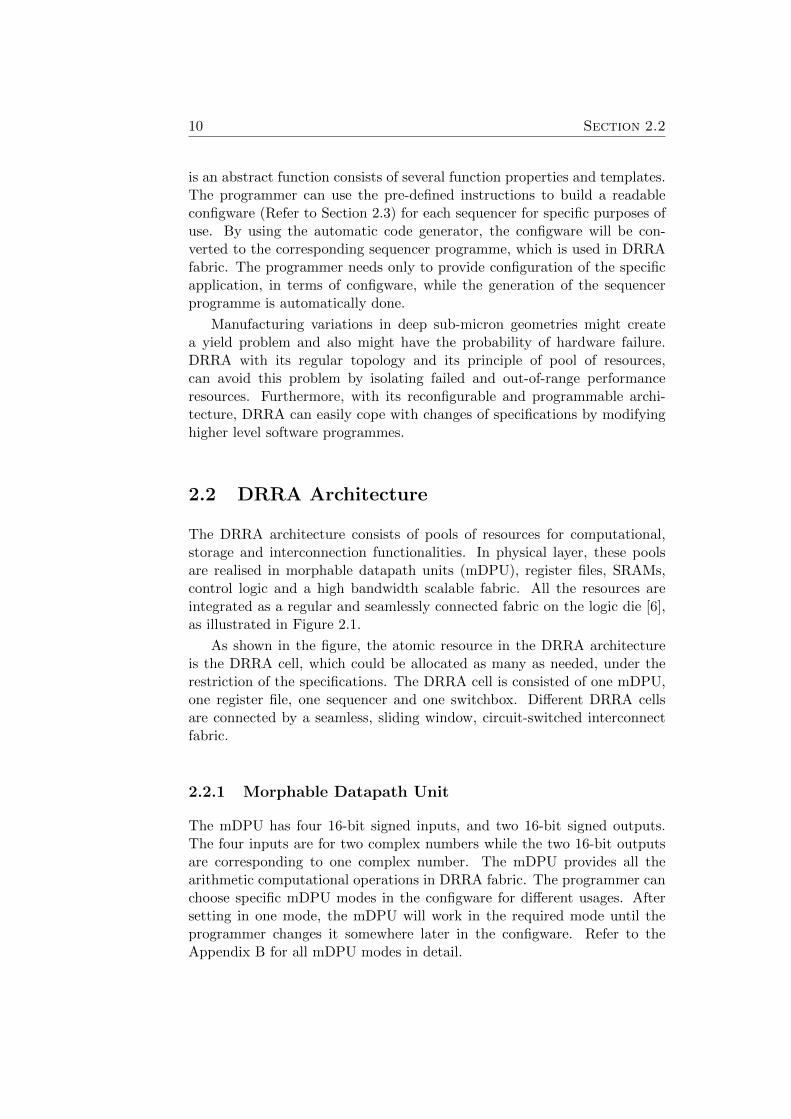
The DRRA architecture consists of pools of resources for computational,storage and interconnection functionalities. In physical layer, these poolsare realised in morphable datapath units (mDPU), register files, SRAMs,control logic and a high bandwidth scalable fabric. All the resources areintegrated as a regular and seamlessly connected fabric on the logic die [6],as illustrated in Figure 2.1.
As shown in the figure, the atomic resource in the DRRA architectureis the DRRA cell, which could be allocated as many as needed, under therestriction of the specifications. The DRRA cell is consisted of one mDPU,one register file, one sequencer and one switchbox. Different DRRA cellsare connected by a seamless, sliding window, circuit-switched interconnectfabric.
2.2.1 Morphable Datapath Unit
The mDPU has four 16-bit signed inputs, and two 16-bit signed outputs.The four inputs are for two complex numbers while the two 16-bit outputsare corresponding to one complex number. The mDPU provides all thearithmetic computational operations in DRRA fabric. The programmer canchoose specific mDPU modes in the configware for different usages. Aftersetting in one mode, the mDPU will work in the required mode until theprogrammer changes it somewhere later in the configware. Refer to theAppendix B for all mDPU modes in detail.

Chapter 2 11
Seamless sliding window DRRA interconnect
DRRA cell
Register fileMorphable datapath unit Sequencer
Input busOutput bus Switchbox
Figure 2.1: DRRA Physical Layer Fabric Architecture
2.2.2 Register File
The register file in DRRA fabric is a 64-word 16-bit register file with tworead and two write ports. The register file has DSP style Address Gen-eration Units (AGU) which are capable with vectorised, circular-bufferedand bit reverse addressing. This ignites the advantage of DRRA handlingwith DSP-intensive applications, for example, Fast Fourier Transformation(FFT). Register files can read or write specified numbers of data starting atgiven addresses, increasingly or decreasingly, either in a linear or non-linearway. And these operations could be executed in a couple of loops or evenin an endless loop. Those read/write actions could be set with an initialdelay and be executed at specific time, providing parallelism between differ-ent read/write actions. Once again, the behaviours of register files could beconfigured by programmers in the configware, specifying ‘start address’,‘number of addresses’, and ‘initial delay’, etc. Refer to AppendixA for Register Files instructions for more detail. Furthermore, the AGU pro-vides an ‘indirect’ way of reading/writing data, whose start address couldbe specified by the corresponding mDPU’s outputs.

12 Section 2.2
2.2.3 Switchbox
Switchboxes provide interconnection between different DRRA cells. Theyconnect mDPUs, register files and sequencers. Switchboxes use the mech-anism of circuit switch by connecting horizontal and vertical buses. Theinputs of mDPU and register files are connected to vertical buses, namely‘vlanes’ in the fabric design, while the outputs of mDPU and register filesare connected to horizontal buses, namely ‘hb mdpu’ and ‘hb reg’. Thehorizontal buses and vertical buses are respectively connected to the inputsand outputs of switchboxes. Therefore by controlling the switchboxes, inputsand outputs can be easily connected. The programmer can use switchboxinstruction in the configware, refer to Appendix A for instruction formats.
Figure 2.2: Reachable DRRA Cells in 3-Hop Local Connectivity Area
DRRA architecture provides seamless sliding window circuit switch net-work. Components in a DRRA cell can communicate with those in anotherDRRA cell column-wisely and row-wisely 3 hops away, either in the left orthe right direction. Thus a cell in the centre of a 7-by-7 sliding windowcan communicate with other cells within this window, as shown in Figure2.2. This local connectivity feature of DRRA reduces delay and energyconsumption.
Chapter 2 13
2.2.4 SRAM Memory
SRAMs could be used in DRRA as peripheral memories for holding data,for example, samples for a DSP application. These data could be writeto register files for further computational use. SRAMs are connected tofixed register files via a special SRAM bus. This bus is 256-bit wide andcan fill and empty a register file within 4 cycles. Each SRAM has its ownAddress Generation Unit and a small local sequencer (SRAM sequencer)which controls the flow of data between SRAMs and register files.
2.2.5 Control Logic
The control logic in DRRA is realised by sequencers, which handle withsingle instruction sequential flow. There are two types of sequencers: aDRRA cell sequencer and an SRAM sequencer. The programme memory ineach sequencer can store maximally 256 instructions.
DRRA Cell Sequencer
As shown in Figure 2.1, a DRRA cell sequencer (Normally when we speakof a sequencer, which refers to a DRRA cell sequencer) controls one mDPU,one register file and one switchbox in one DRRA cell. Sequencers can pro-vide availabilities of conditional and counter based loop and branching. Toprogramme the functionalities of DRRA fabric is actually to programmethe behaviours of the sequencers. The programmer will write/configure afile called configware containing instructions for mDPU, register file andswitchbox. The sequencer will execute these instructions sequentially andsend instruction signals to the specific components. As we can see in Figure2.1, a programmer can only manipulate the components within one DRRAcell. In addition, sequencers have hierarchical control signals, which makeit possible for different sequencers in other reachable DRRA cells to coor-dinate with each other, in order to complete more difficult tasks. Thesehierarchical signals are controlled by using hierarchical control instructions,whose description, as well as all the sequencer instructions, could be foundin Appendix A.
SRAM Sequencer
An SRAM Sequencer can only control the behaviours of SRAMs. It has noconnectivity controls and hierarchical controls. An SRAM sequencer cancontrol the behaviours of SRAMs, such as read/write data from/to SRAMs.Also, the instructions of SRAM sequencer can be found in Appendix A.

14 Section 2.4
2.3 DRRA Design Flow
The DRRA Design Flow could be illustrated in Figure 2.3. As we can seein the design flow, a project is divided into two parts: physical design flowand application mapping flow. According to hardware specifications, forexample approximate area, working speed, etc., the physical designer willallocate DRRA coarse grain atomics (DRRA cells, memory banks) to buildan unconfigured DRRA fabric. According to the functional specifications, asoftware programmer will design an algorithm based on the basic mechanismof DRRA fabric. Afterwards, he or she will use pre-defined instructions andDRRA library to write a configuration programme, namely, ‘configware’. Aconfigware in DRRA is an assembly-like code for configuration of sequencers.It is a sequential programme executed by sequencer, providing conditionaland counter-based loop and branching. It uses DRRA’s pre-defined instruc-tions and libraries to control the sequencer to send out control signals toother components within a DRRA cell (or an SRAM), and send out hierar-chical control signals within the reachable local connectivity area.
Then a hardware compiler will configure the DRRA fabric according tothe configwares. The output will be a configured DRRA fabric. At thisstage, the DRRA fabric is at register-transfer level (RTL). Thus simulationand verification are done to see whether the design meets the functionalspecification: logic, timing, etc. If there are some variations, either physicaldesigner shall change the fabric allocation or the programme shall modifythe configwares (In most cases it is mainly the software issue), or both. Afterthe modifications, another check will be done through the new configuredfabric.
If the fabric meets the functional specifications, the RTL fabric will besynthesised into a gate-level netlist. Again gate-level simulation and veri-fication will be carried out for checking the validity in both physical andfunctional aspects. If it does not meet the specifications and constraints,further modifications need to be done in physical design and applicationmapping. In most cases modifications are about the physical allocations.
2.4 CDMA Modes of mDPU
The mDPU can be configured for CDMA-based applications. It can be usedto achieve channelisation and scrambling operations, which could be usedin the 3G mobile communication systems. In this section we discuss someof the mDPU modes specially designed for CDMA, which are used in ourcorrelation pool design. All the usages of each mode could be found inAppendix B in detail.

Chapter 2 15
Figure 2.3: DRRA Design Flow

16 Section 2.4
2.4.1 Code Generation Mode
The principles of generating OVSF code and scrambling code are discussedin Chapter 1.
As we introduced earlier, data symbols should be spread over a widespectrum range before transmitting to increase bandwidth. Every symbol istranslated into a number of chips. The number of chips per symbol is calledspreading factor (SF). In our design, mDPUs can achieve the value of SFfrom 8 to 256 (2n, where n = 3, 4, 5, 6, 7, 8).
Figure 2.4: Serial OVSF Code Generator
In our mDPU, we use serial OVSF code generator to reduce gate count,also making it power efficient. Our SF is maximally 28, thus 8-bit indexregisters and counter registers are used, as shown in Figure 2.4. In thefigure, the XOR block does exclusive-or operation bit-wisely for all the ANDoutputs, and the result is inverted for the final OVSF code. Thus in thisdesign we only have an 8-bit counter, 8 AND gates, 8 XOR gates and aninverter.
Refer to Figure 1.7 in Chapter 1 for the concepts of scrambling codesgeneration. It is basically implemented in the mDPU in the same way asthe figure indicates. The long scrambling sequences are generated by meansof two generator polynomials of degree 25. The polynomials can be config-ured for generating different scrambling sequences (also called ‘scramblingcodes’). Since our mDPU’s inputs have the bit width of 16, we have to takentwo steps (lower 16 bits and then higher 16 bits) to put the whole scramblingcode generator polynomial in the mDPU’s 25-bit width scrambler registers

Chapter 2 17
(for example, ScramblerReRegister0, ScramblerImRegister0).Afterwards, the real part and imaginary part of the scrambling code
(The two long sequences clong,1,n and clong,2,n in Figure 1.7) respectivelydoes exclusive nor (XNOR) operation with generated OVSF code. Thenthe results could be put to mDPU’s outputs as generated correlation codes.The 16-bit output code format can be shown in Figure 2.5.
Figure 2.5: Format of the Output Correlation Codes
The output is in a format of interpreting complex number, where thelogic value ‘1’ and ‘0’ are assigned to ‘1’ and ‘-1’, respectively. For example,if the output is (in hexadecimal) ‘0x0100’, it stands for the complex number1− j.
In our mDPU, since we have four 16-bit inputs and two 16-bit outputs,we can process two sets of codes in parallel. Thus we have two sets ofduplicated code generation mechanism that we mentioned above.
2.4.2 Vector Rotation Mode
In this mode, mDPU can multiply two complex samples by their correspond-ing codes generated by another mDPU working in ‘code generation’ mode.The format of the input complex samples are shown in Figure 2.6.
Figure 2.6: Format of the Input Complex Samples
The 16-bit mDPU inputs take samples in complex form, with higher 8bits for the signed in-phase part, while lower 8 bits for the signed quadraturepart, as the figure indicates. For example, if the input complex data is (inhexadecimal) ‘0xE818’, it indicates the complex number −24 + 24j.
In the ‘vector rotation’ mode, mDPU multiplies the complex sam-ples and generated correlation code, and accumulates the result in a register.

18 Section 2.5
Input data Code Multiplication Result
I + Qj
1 + j (I −Q) + (I + Q)j1− j (I + Q)− (I −Q)j−1 + j −(I + Q) + (I −Q)j−1− j −(I −Q)− (I + Q)j
Table 2.1: Complex Multiplication Results
As Table 2.1 indicates, there are only four cases of complex number mul-tiplication in this mode. According to Nasim [5], all computations in thismode could be performed using adders and subtractors. This solution cansave a lot of gate counts by avoiding using multipliers. The output of the‘vector rotation’ mode will be the sum of the products of input data(inthe format of I +Qj) and the codes (in the format of ±1+±j), which couldbe written:
output =∑
(I + Qj)× (±1 +±j)
The outputs are also 16 bits, thus the overflow issue of both real andimaginary part should be taken care of.
2.4.3 Other Modes
There are other mode manipulating mDPU for putting data in specific regis-ters. For example, the mode ‘m SRL in’ reads the scrambling code generatorpolynomial configuration for the lower 16 bits of the long scrambling codeclong,1,n in the scrambling register, while ‘m SRH in’ reads the higher 7 bitsfor clong,1,n; the mode ‘m UID out’ is putting out the user ID from its reg-ister through the 16-bit outputs; the mode ‘m bypass’ is putting the input0 and input 2 directly to the output 0 and output 1. The principles of thesemodes are simple and their usages could be easily found in Appendix B,thus more details are not extracted here.
2.5 Summary
In this chapter, we described the DRRA hardware platform in detail forthis thesis project. We firstly introduced the innovations and advantages ofthe principle of DRRA, to highlight its novelties and efficiency for multime-dia applications which emphasise on digital signal processing. The wholeDRRA architecture is described and analysed, including mDPU, registerfiles, switchbox, and sequencer, etc. Furthermore, some important mDPUmodes crucial for the implementation of “Correlation Pool” are also covered.

Chapter 3
Correlation Pool in DRRA
3.1 Multi-Finger Correlation Pool Specifications
The principles of correlation pool in WCDMA are discussed in Chapter 1,here we give brief introduction of the technical specifications.
1. Functional requirements:
• The sampling frequency can achieve 2×chiprate = 2×3.84 Mbps;
• The system can process minimally 1024 fingers;
• The spreading factors (SF) can be chosen from 8 to 256.
• The sample bitwidth for both in-phase (I) and quadrature (Q) is8-bit.
2. Performance requirements:
• The latency of the system can be no larger than 256 chips;
• The total gate count is less than 500 k/mm2;
• The average power consumption is less than 100 mW.
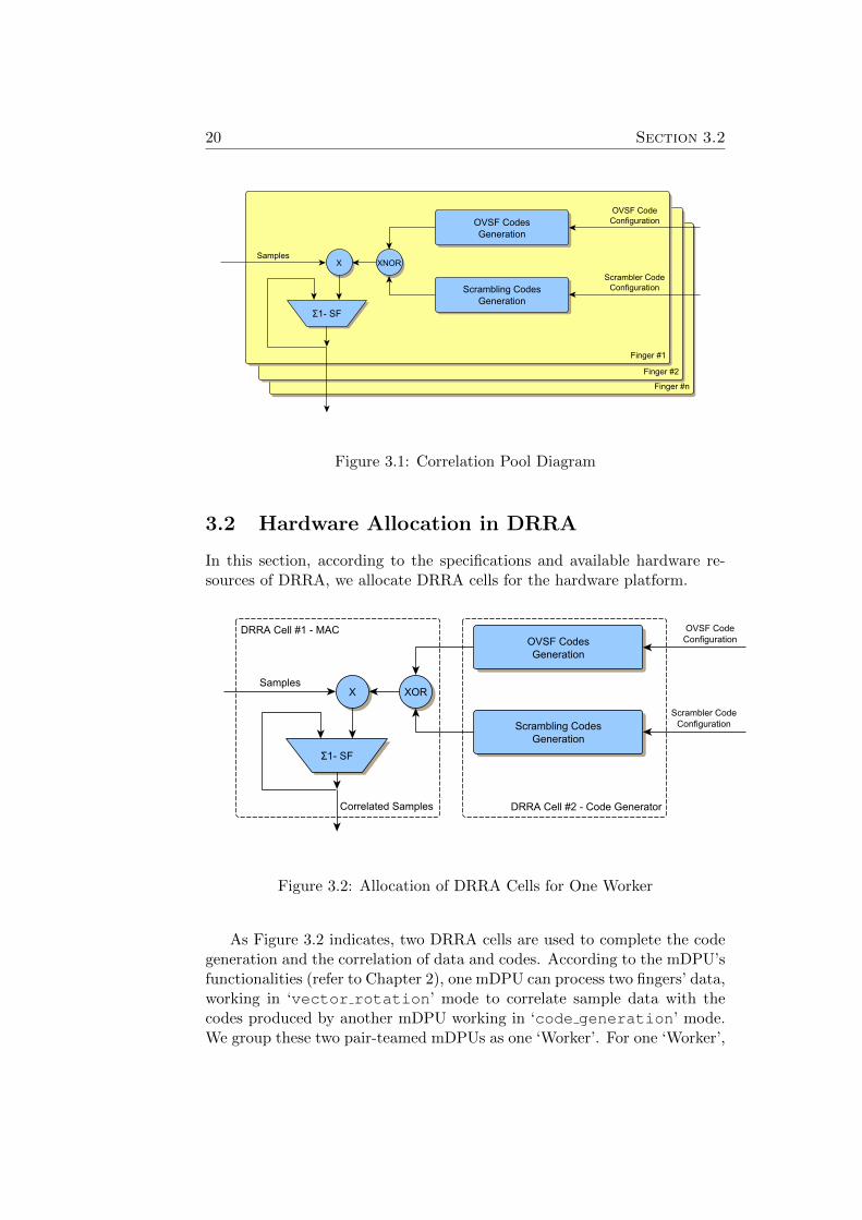
The block diagram of of the correlation pool can be illustrated in Figure3.1. As we discussed in Chapter 2, users can configure and select specificthe OVSF and scrambling codes by external signals. The sample data, withthe bit width of 8 for both in-phase (I) and quadrature (Q) are correlatedwith the generated OVSF codes and scrambling codes. The the whole samplefirst enters the correlation pool and then correlates with the codes bit-wisely.Afterwards the correlated bits are accumulated according to ‘SF’. The resultof the accumulation generates the correlated sample, which will be outputfor further process. This is for one finger. In this thesis project, the systemaims to process at least 1024 fingers.
20 Section 3.2
Figure 3.1: Correlation Pool Diagram
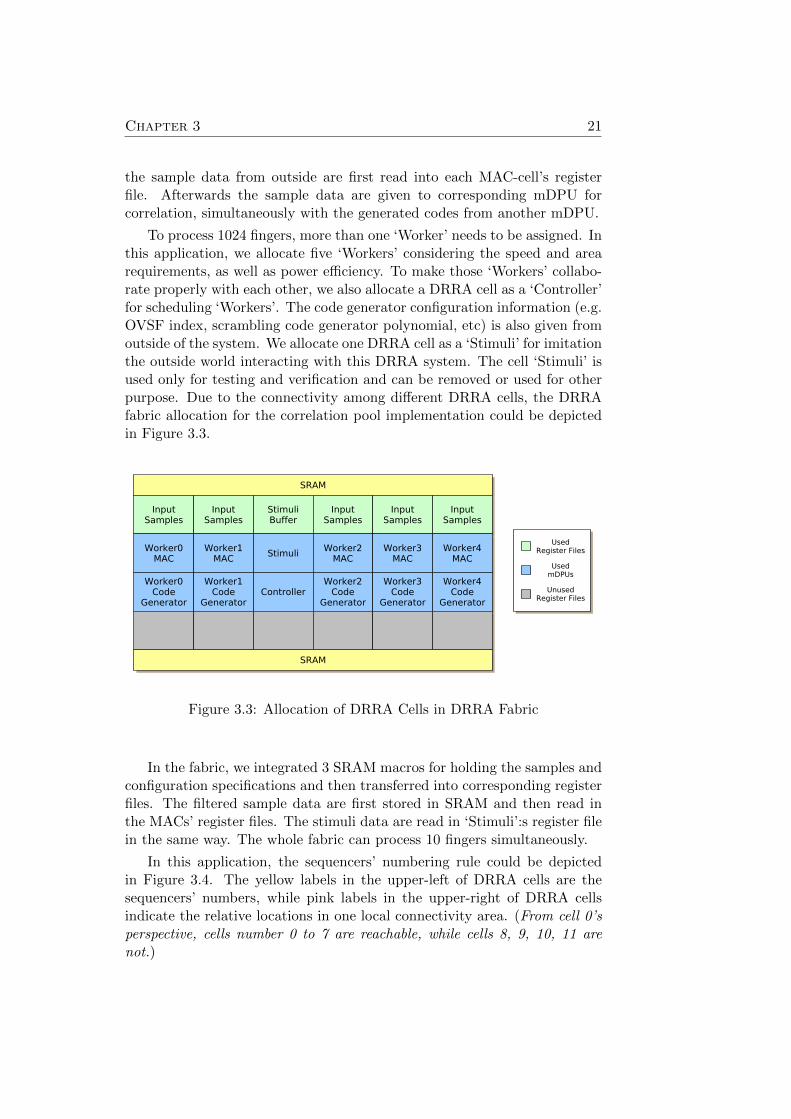
3.2 Hardware Allocation in DRRA
In this section, according to the specifications and available hardware re-sources of DRRA, we allocate DRRA cells for the hardware platform.
Figure 3.2: Allocation of DRRA Cells for One Worker
As Figure 3.2 indicates, two DRRA cells are used to complete the codegeneration and the correlation of data and codes. According to the mDPU’sfunctionalities (refer to Chapter 2), one mDPU can process two fingers’ data,working in ‘vector rotation’ mode to correlate sample data with thecodes produced by another mDPU working in ‘code generation’ mode.We group these two pair-teamed mDPUs as one ‘Worker’. For one ‘Worker’,
Chapter 3 21
the sample data from outside are first read into each MAC-cell’s registerfile. Afterwards the sample data are given to corresponding mDPU forcorrelation, simultaneously with the generated codes from another mDPU.
To process 1024 fingers, more than one ‘Worker’ needs to be assigned. Inthis application, we allocate five ‘Workers’ considering the speed and arearequirements, as well as power efficiency. To make those ‘Workers’ collabo-rate properly with each other, we also allocate a DRRA cell as a ‘Controller’for scheduling ‘Workers’. The code generator configuration information (e.g.OVSF index, scrambling code generator polynomial, etc) is also given fromoutside of the system. We allocate one DRRA cell as a ‘Stimuli’ for imitationthe outside world interacting with this DRRA system. The cell ‘Stimuli’ isused only for testing and verification and can be removed or used for otherpurpose. Due to the connectivity among different DRRA cells, the DRRAfabric allocation for the correlation pool implementation could be depictedin Figure 3.3.
Figure 3.3: Allocation of DRRA Cells in DRRA Fabric
In the fabric, we integrated 3 SRAM macros for holding the samples andconfiguration specifications and then transferred into corresponding registerfiles. The filtered sample data are first stored in SRAM and then read inthe MACs’ register files. The stimuli data are read in ‘Stimuli’:s register filein the same way. The whole fabric can process 10 fingers simultaneously.
In this application, the sequencers’ numbering rule could be depictedin Figure 3.4. The yellow labels in the upper-left of DRRA cells are thesequencers’ numbers, while pink labels in the upper-right of DRRA cellsindicate the relative locations in one local connectivity area. (From cell 0’sperspective, cells number 0 to 7 are reachable, while cells 8, 9, 10, 11 arenot.)
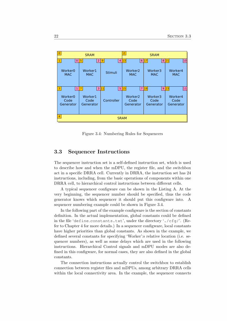
22 Section 3.3
Figure 3.4: Numbering Rules for Sequencers
3.3 Sequencer Instructions
The sequencer instruction set is a self-defined instruction set, which is usedto describe how and when the mDPU, the register file, and the switchboxact in a specific DRRA cell. Currently in DRRA, the instruction set has 24instructions, including, from the basic operations of components within oneDRRA cell, to hierarchical control instructions between different cells.
A typical sequencer configware can be shown in the Listing A. At thevery beginning, the sequencer number should be specified, thus the codegenerator knows which sequencer it should put this configware into. Asequencer numbering example could be shown in Figure 3.4.
In the following part of the example configware is the section of constantsdefinition. In the actual implementation, global constants could be definedin the file ‘define constants.txt’, under the directory ‘./cfg/’. (Re-fer to Chapter 4 for more details.) In a sequencer configware, local constantshave higher priorities than global constants. As shown in the example, wedefined several constants for specifying ‘Worker’:s relative location (i.e. se-quencer numbers), as well as some delays which are used in the followinginstructions. Hierarchical Control signals and mDPU modes are also de-fined in this configware, for normal cases, they are also defined in the globalconstants.
The connection instructions actually control the switchbox to establishconnection between register files and mDPUs, among arbitrary DRRA cellswithin the local connectivity area. In the example, the sequencer connects

Chapter 3 23
its own cell’s register file’s inputs to another mDPU’s output in anotherDRRA cell numbered as ‘work loc 1’.
0 /* Sequencer Instructions Example */1 /* Sequencer Number */2 USE SEQ 234 /* Constants Definition */5 #DEFINE CONST work_loc_0 2;6 #DEFINE CONST work_loc_1 4;7 #DEFINE CONST RFILE_range 4;8 #DEFINE CONST init_dly 2;9 #DEFINE CONST opt_dly 4;
1011 #DEFINE CONST HC_RTS 1;12 #DEFINE CONST HC_CTS 0;1314 #DEFINE CONST m_cg 9;15 #DEFINE CONST m_bypass 17;1617 /* Connections */18 CONNECT REFI work_loc_0 IN 0 to DPU work_loc_1 OUT 0;19 CONNECT REFI work_loc_0 IN 1 to DPU work_loc_1 OUT 1;2021 /* Hierarchical Control */22 /Start/ HCWAIT wait work_loc_1 HC_RTS Read 0;23 /Read/ HCOUT send 1 0 0 0 0 HC_CTS 0;2425 /* Register File Operations */26 RFILE1 rfileinstr RA 1 linear 0 RFILE_range + 1 init_dly 3 YES NO;27 RFILE1 rfileinstr RB 1 linear 0 RFILE_range + 1 init_dly 3 YES NO;2829 /* mDPU Operations */30 MDPU mdpuinstr m_cg 0 0 3 3 0 0;31 DELAY delayinstr opt_dly 0;3233 MDPU mdpuinstr m_bypass 0 0 0 0 0 0;34 JUMP tothe address Start 0;
Listing 3.1: An Example of Sequencer Configware
The Hierarchical Control (HC) instructions define the HC output of aDRRA cell, and based on what value from which DRRA cell should thecurrent cell perform what kind of actions. For example, in the configwareListing A, the current sequencer waits until the sequencer ‘work loc 1’(which is 4) sends an HC signal ‘HC RTS=1’, and it jumps to branch labelled‘/Read/’. (In our sequencer instruction structure, programmers could pro-vide names for indicating different instructions by adding labels with twoslashes, e.g. ‘/Label/’.) And then in the branch ‘/Read/’, it broadcastsanother HC signal ‘HC CTS=0’. In the meanwhile the cell 4 will listen this‘HC CTS=0’ for sending expected data. This is used as a handshake proto-col between different cells. HC waiting and conditional branching provide

24 Section 3.4
inter-cell synchronisation no matter their action cycles are predictable ornot.
It is possible to use these sequencer instructions to programme the se-quencer to control the mDPU, the register file and the switchbox withinone DRRA cell and several other sequencers by using hierarchical controlsignals. In the example configware Listing A, it describes the behaviours ofregister file and mDPU. Here it reads the register file from both input portsfor 5 data and then switches its mDPU to ‘code generation’ mode.
The ‘DELAY’ instruction is a multi-cycle no-operation instruction. It isused in most cases for predictable delays. For example in this case, whenmDPU is switched to ‘code generation’ mode, it will keep this modeuntil changed. Thus this delay can keep the mDPU working in specific modefor specific delays until the next instruction changes the mode to ‘bypass’mode. Then ‘JUMP’ instruction unconditionally jumps the configware to theline labelled ‘/Start/’.
By explaining the example configware, we have covered the basic struc-ture and most common-used instructions in a DRRA configware. By pro-gramming different cofigwares in each sequencer, a DRRA fabric can achievedifferent goals of applications, from control systems to high performancedigital signal processing applications. For more details of sequencer instruc-tions, refer to Appendix A.
3.4 Algorithm and Implementation
In this section, we will discuss how the algorithms work in each type ofDRRA cells.
3.4.1 Stimuli and Controller
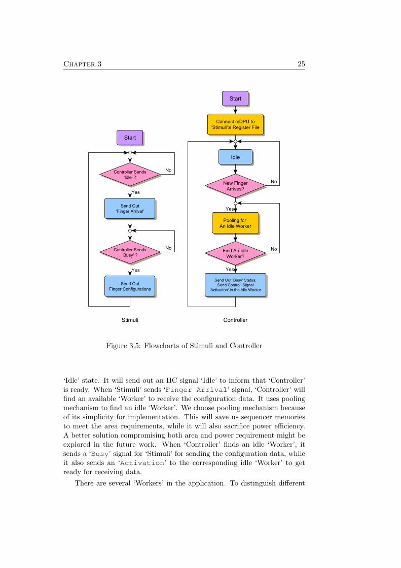
The flowcharts for ‘Stimuli’ and ‘Controller’ could be depicted in Figure3.5. For ‘Stimuli’, it waits ‘Controller’ to send an ‘Idle’ HC signal after itsinitialisation. As soon as it hears the ‘Idle’ signal, it sends a ‘FingerArrival’ signal, indicating that there are finger data to be processed.When ‘Controller’ receives this signals, it starts to find available workersfor processing. As soon as ‘Controller’ finds an idle worker, it sends outa ‘Busy’ signal for ‘Stimuli’. When ‘Stimuli’ hears the ‘Busy’ signal from‘Controller’, it reads its own register file for sending out the pre-stored fingerconfigurations. After sending one finger’s configuration data, it goes backto wait ‘Controller’ sends another ‘Idle’ signal.
For ‘Controller’, in the initialisation stage, it connects its mDPU’s inputsto the register file’s outputs of ‘Stimuli’. When ‘Stimuli’ reads its registerfile, the data will be output on the mDPU’s inputs of ‘Controller’. Then themDPU switches to ‘bypass’ mode, it put the inputs directly to the outputs,introducing one cycle delay. After these operations, ‘Controller’ goes into
Chapter 3 25
Figure 3.5: Flowcharts of Stimuli and Controller
‘Idle’ state. It will send out an HC signal ‘Idle’ to inform that ‘Controller’is ready. When ‘Stimuli’ sends ‘Finger Arrival’ signal, ‘Controller’ willfind an available ‘Worker’ to receive the configuration data. It uses poolingmechanism to find an idle ‘Worker’. We choose pooling mechanism becauseof its simplicity for implementation. This will save us sequencer memoriesto meet the area requirements, while it will also sacrifice power efficiency.A better solution compromising both area and power requirement might beexplored in the future work. When ‘Controller’ finds an idle ‘Worker’, itsends a ‘Busy’ signal for ‘Stimuli’ for sending the configuration data, whileit also sends an ‘Activation’ to the corresponding idle ‘Worker’ to getready for receiving data.
There are several ‘Workers’ in the application. To distinguish different

26 Section 3.4
‘Workers’, each generator has a unique ID and waits its own ‘Activation’signal. When ‘Controller’ sends the ‘Activation’, it actually sends aspecific ‘Activation’ signal for the specific ‘Worker’.
Here ‘Controller’ provides the synchronisation between ‘Stimuli’ and‘Worker’. It passes the configuration information from ‘Stimuli’ to ‘Worker’by using the ‘bypass’ mode. Then it delays specific cycles for transferringconfigurations and then returns to ‘Idle’ state.
3.4.2 Code Generator
Figure 3.6: Flowchart of Code Generator
The flowchart for ‘Code Generator’ could be depicted in Figure 3.6. Inthe initialisation stage, ‘Code Generator’ connects its mDPU’s inputs tothe mDPU’s outputs of ‘Controller’. As described earlier, when ‘Stimuli’reads its register file, the outputs will be put on the mDPU’s inputs of

Chapter 3 27
‘Controller’, due to the connection we established. The ‘Controller’:s mDPUworks in the ‘bypass’ mode, it passes the inputs directly to the outputs.As a result, when ‘Stimuli’ reads its register file to send configuration data,‘Code Generator’ will receive it after one cycle delay. Afterwards, ‘CodeGenerator’ goes into ‘Idle’ state, sending out an ‘Idle’ signal and waitingfor its own ‘Activation’ signal from ‘Controller’.
When ‘Code Generator’ receives the HC signal ‘Activation’, it turnsinto ‘Busy’ state. It sends out a ‘Busy’ signal and is ready for receivingthe configuration data. It will take 6 cycles for ‘Code Generator’ to putthe configuration data in different registers, namely, user ID, code indexes,long scrambling code lower 16 bits and higher 7 bits for two fingers. Thisprocedure requires the mDPU to change different modes to accomplish.
After receiving the configuration data, the mDPU switches to the mode‘code generation’. In this mode, the mDPU will keep on generating cor-relation codes based on the configurations. A predictable delay, ‘code gen dly’,could be set for generating desired number of codes according to the SpreadFactor. These codes are put on the outputs of mDPU and connected to‘MAC’ for sample data correlation.
When finishing the code generation, ‘Code Generator’ will also outputthe current finger’s long scrambling code as results, labelling with user ID.Then it changes its mDPU to ‘bypass’ mode and returns to ‘Idle’ state.
3.4.3 Complex Multiplier-Accumulator
The flowchart for the Complex Multiplier-Accumulator (MAC) is shown inFigure 3.7. The ‘MAC’ cell accomplishes the task of correlating the sampledata with the correlation codes. The sample data are stored in ‘MAC’ cell’sregister file. The complex sample data are stored in the format of Figure2.6.
In the beginning, ‘MAC’ is in the ‘Idle’ state. It sends out an HC signal‘Idle’ and waits for ‘Controller’ to signal ‘Activation’. Similar as ‘CodeGenerator’, ‘MAC’ waits for its own ‘Activation’, to distinguish fromother ‘MACs’. However, the ‘Activation’ signal is the same for both‘Code Generator’ and ‘MAC’ in the same ‘Worker’.
When ‘MAC’ hears its own ‘Activation’ signal, it sends out a ‘Busy’signal, informing ‘Controller’ that it is not available when new finger ar-rivers. Then it establishes a connection between the mDPU’s outputs of‘Controller’ and its own mDPU’s inputs, for receiving the configuration datafrom ‘Stimuli’ (outside environment). The configuration data for ‘MAC’ isspecifically the starting address to read its register file for sample data.
After receiving the starting address, ‘MAC’ switches its mDPU’s inputsto its own register file’s outputs and the mDPU’s outputs of ‘Code Genera-tor’. This is intend to read the sample in the register file, and to receive thecorrelation codes from ‘Code Generator’ simultaneously, thus the mDPU of

28 Section 3.5
Figure 3.7: Flowchart of Complex MAC
‘MAC’ can accomplish the task of correlation. In the meanwhile, the mDPUswitches to work in the mode ‘vector rotation’. Afterwards, the samepredictable delay ‘code gen dly’, the same as ‘Code Generator’ has, is setfor the synchronisation of correlation. The correlated data are output whenfinished.
Then ‘MAC’ returns to ‘Idle’ state and sends out the Hierarchical Controlsignal ‘Idle’.
3.5 Timing Graph of Control and Communication
To implement the algorithms we stated previously, configware programmesneed to be written for each sequencer. Refer to Appendix C for the detailed

Chapter 3 29
Wai
ts
`Id
le’
fro
m
`Co
ntr
olle
r’
Sen
ds
`Id
le’
Sen
ds
`FA
’
Wai
ts
for
`FA
’
Wai
ts f
or
an id
le
`Wo
rker
’
Sen
ds
`Id
le’
`Act
#n
’ an
d
`Bu
sy’
Wai
ts f
or
`Bu
sy’ f
rom
`C
on
tro
ller’
Wai
ts f
or
`Act
ivat
ion
#n
’ fro
m
`Co
ntr
olle
r’
Pas
ses
Co
nfi
g In
fo.
Sen
ds
Co
nfi
g In
fo.
Rec
eive
s
Co
nfi
g In
fo.
Sen
ds
`Id
le’
`Bu
sy’
Co
rrel
atio
n in
pro
gres
s
Sen
ds
ou
t `I
dle
’
Wai
ts f
or
an id
le
`Wo
rker
’
Sen
ds
`Id
le’
Wai
ts f
or
`Act
ivat
ion
#m
’ fro
m `
Co
ntr
olle
r’
Wai
ts f
or
`Bu
sy’ f
rom
`C
on
tro
ller’
Wai
ts
for
`FA
’
Wai
ts f
or
`Act
ivat
ion
#n
’ fro
m `
Co
ntr
olle
r’
`Bu
sy’
Co
rrel
atio
n
Stim
uli
(Ou
tsid
e En
viro
nm
ent)
Co
ntr
olle
r
Wo
rker
n
Wo
rker
m
28
5 c
ycle
s
Wai
ts
`Id
le’
fro
m
`Co
ntr
olle
r’
Sen
ds
`FA
’
`Act
#m
’ an
d
`Bu
sy’
Sen
ds
Co
nfi
g In
fo.
Pas
ses
Co
nfi
g In
fo.
Rec
eive
s
Co
nfi
g In
fo.
Sen
ds
`Id
le’
Wai
ts
`Id
le’
fro
m
`Co
ntr
olle
r’
`FA
’ = `
Fin
ger
Arr
ives
’ ; `
Act
’ = `
Act
ivat
ion
’
...
...
...
...
Figure 3.8: Timing Graph of Correlation Pool

30 Section 3.6
codes.In the correlation pool control logic, we are using pooling mechanism.
The timing graph describing the control and communication processes couldbe depicted in Figure 3.8. As we can see in the figure, ‘Stimuli’ (outsideenvironment) will first have a handshake with ‘Controller’, and then when-ever there is an idle ‘Worker’, ‘Stimuli’ can send the finger configurationinformation to ‘Controller’. The ‘Controller’ is responsible for passing theinformation to the corresponding idle ‘Worker’. In ‘Workers’ pooling mech-anism, each ‘Worker’ has its own index number, the smaller the number is,the higher priority ‘Worker’ has, as it shows in Figure 3.8. The processingof two fingers in one ‘Worker’ will take 285 cycles, other waiting delays areunpredictable, depending on how frequent ‘Stimuli’ sends the finger config-urations.
3.6 Summary
In this chapter we discussed about how the correlation pool is implementedin DRRA platform. We presented the specifications for the product of thethesis project and the allocated DRRA hardware for meeting the hardwarerequirements. Afterwards, algorithms for correlation pool are extracted,with control flows for different DRRA atoms involved. Lastly, we also in-cluded the control timing graph for processing sample data.

Chapter 4
System Verification
4.1 Project Directory Structure
RootCP_Project
CP_Verification Library_File
RTL Netlist
Fabric_VHDL
C# VHDLTestbenches
Results ScriptsConfigware
bin cfg vhdl_sectionsseq instructionsoutput
Figure 4.1: Directory Structure of Correlation Pool Project
Figure 4.1 shows the directory structure of the whole project ‘CP Project’.We are using TSMC 65nm GP Standard Cell Libraries for this project, thelibrary files are placed in the the directory ‘Library Files’. The resourcefiles are placed in the folder ‘Fabric VHDL’, as the sub-folders’ names sug-gest, ‘RTL’ contains the register-transfer level VHDL codes, while ‘Netlist’contains the synthesised gate level netlists.
The directory ‘CP Verification’ contains all the files that are usedduring the verification, including VHDL testbenches, simulation scripts, the

32 Section 4.2
golden model generator, the comparator for golden model and “CorrelationPool” simulation results, as well as the simulation results. Under the di-rectory ‘Configware’ placed the MANAS Tool, which is used to translatesequencer configwares into VHDL testbenches. The testbenches are used forsimulation of the configured DRRA system. We will extract this in Section4.2.
4.2 The MANAS Tool
MANAS (MANual ASsembly) is a tool for translating sequencer configwares(assembly code) to VHDL testbenches.
4.2.1 MANAS Directory Structure
As Figure 4.1 shows, the folders for MANAS are:
• bin, contains the executable MANAS bin file;
• cfg, contains the definitions of global constants, in the file‘define constants.txt’;
• seq, contains the sequencer configwares, with the names of ‘seqXX.txt’,where ‘XX’ indicates the sequencer numbers of different DRRA cells;
• output, contains the translated VHDL testbenches. There will befour generated testbenches in this folder. The testbenches are:
– tb test non mem RTL.vhd;
– tb test mem RTL.vhd;
– tb test non mem gatelevel.vhd;
– tb test mem gatelevel.vhd.
They are the combinations of any two of the cases: RTL/gate-leveland with/without SRAM. We use those testbenches with memory forverification. All the testbenches have the same functionality. The test-bench combines all the sequencer configwares and put the instructionssequentially in the corresponding sequencers;
• instructions, contains the definitions of sequencer instructions, inthe files ‘default intsrs.txt’ and ‘instructions format.txt’;
• vhdl sections, contains the VHDL template files and initial valuesof SRAMS. The files:
– head *.txt;
– middle *.txt;

Chapter 4 33
– tail *.txt.
These files are the VHDL testbench templates. MANAS will use thesefiles to generate testbenches for both register-transfer level and gatelevel.
– manas package.vhd;
– testbench types n constants.vhd.
These two files contains types and constants which are used for test-benches. MANAS will generate them according to instruction formats.
– sample data.vhd.
This file contains the sample data for each the register files of each‘Worker’ to store. The data are written in decimal and in the form ofcomplex numbers shown in Figure 2.6.
4.2.2 Using MANAS
After providing the sequencer configwares in the seq folder and sample datain ‘sample data.vhd’, execute the MANAS executable binary in the binfolder. There are no arguments are required, but root authentication mightbe required. Then the testbenches are created automatically.
4.2.3 Testbench Structure
The testbench has a structure shown in Figure 4.2.
BusIn BusOutDRRA Fabric
Testbench
Instructions Sequencer Indices
Instruction Load
clk
reset_n
Figure 4.2: Testbench Structure

34 Section 4.4
As shown in the figure, besides assigning clock ‘clk’ and ‘reset n’ tothe DRRA fabric, the testbench has a data bus going into the fabric, whichwrites sample data stored in the file ‘sample data.vhd’ into the SRAMmacros. The testbench has also a data bus to read out data from SRAM.
An ‘instruction load’ signal is asserted to load the instructions intocorresponding sequencers, according to the sequencer indices addressed ineach configware (Refer to Figure 3.4 for the sequencer indices).
The outputs are recorded and sent out for the comparison with the goldenmodels. In this application, the golden models are generated by a C#programme.
4.3 Synthesis Results
4.3.1 Technology
The technology we used in this project is TSMC 65nm GP Standard CellLibraries. The synthesis is carried out using Cadence R© Encounter R© RTLCompiler version 9.1. A top-down synthesis flow with clock gating optionfor registers greater than 8 bits is performed.
4.3.2 Critical Path
The critical path starts from the register file’s output, via DPU and ends atthe pipelined multiplier. The critical path is 2.22 ns long, ensuring to meetthe minimal required 450 MHz operating speed.
4.3.3 Gate Count
Since the synthesis tool reports area, we have converted the area into gatecount using a conversion factor of 425 k gates/mm2. We have also esti-mated the area of SRAM meomory macros using Europractice Service andconverted it to gate count using the same conversion factor. The gate countof the DRRA fabric is 426 k gates and that of SRAM macros is 91 k gates.As a result the total gate count of the DRRA fabric including the SRAM is517 k gates.
4.3.4 Power Consumption Estimation
To estimate power consumption, the gate level netlist is simulated and thecorresponding VCD (Value Change Dump) file is created and imported intoCadence R© Encounter R© RTL Compiler. The power consumption estimationafter gate level simulation of Correlation Pool is 76 mW.

Chapter 4 35
4.4 Functional Verification Methodology
In software and hardware design of complex systems, more time and effort isspent on verification than on construction. Simulation is the most popularhardware verification technique and is used in various design stages, e.g.,at register-transfer level, gate and transistor level. Stimulus are given fordifferent configurations and input data. Based on stimuli, execution pathsof the chip model are examined using a simulator. A mismatch between thesimulator’s output and the output described in the specification determinesthe presence of bugs or faults.
To simulate the hardware fabric, MentorGraphics R© ModelSim R© version6.6 is used. We do not extract the systematically module check and simula-tion processes here. They were done prior to the verification of the system.By applying the testbenches for both register-transfer level and gate level,we monitor the ‘MAC’ mDPUs’ outputs for the correlated data. Those dataare recorded using ‘write list’ command of ModelSim R© and they arerecorded in the file ‘all mac out.lst.’
To describe the specification outputs, we use higher level language todescribe the correlation pool in behaviour level. We use C# to model thehardware fabric, using the same provided data. A verification tool contain-ing golden model generator, the comparator for golden model and “Corre-lation Pool” simulation results, is built using C#. The functionalities aredeveloped exactly the same as the the algorithm described in Section 3.4.The generated golden models are recorded in the result files and furthercompared with the hardware simulation results.
4.4.1 Verification Flow
Figure 4.3: Correlation Pool Verification Flow

36 Section 4.4
The verification flow is depicted in Figure 4.3. The verification tool wedeveloped is used to process the verification flow.
As shown in the figure, there are five steps for the verification:
Step 1 The verification tool modifies the configware ‘seq9.txt’ in thesequencer ‘Stimuli’. ‘Stimuli’ provides the input fingers. In principle,we can provide as many fingers as possible, however since we use aDRRA cell as ‘Stimuli’, due to the restriction of sequencer memory,we can provide at most 9 fingers of each verification.
Step 2 The verification tool will randomly generate the sample data foreach ‘MAC’. The data are presented in complex number according therestrictions of specification. Those data are generated and written inthe file ‘sample data.vhd’, in the folder‘./CP Verification/Configware/vhdl sections/’.
After Step 1 and Step 2, the stimulus and data are ready for bothtestbenches (register-transfer level and gate level) and the golden modelgenerator.
Step 3 Execute MANAS to compile the configwares into testbenches. TheDRRA fabric testbenches are the outputs of this step. When simulat-ing the correlation pool, the verification tool will write the simulationresult in the file ‘all mac out.lst’. In the meanwhile, the goldenmodel generator of the verification tool will generate the expected re-sults from the algorithms realised in C#. Those two results will furtherbe compared in Step 4. The golden model generator uses the samestimulus and data as those used in DRRA fabric, which are preparedin Step 1 and Step 2.
Step 4 The C# verification tool will compare the results generated fromtwo variations of implementations, the DRRA implementation and thegolden model in C#. Any mismatches between the two results will bereported.
Step 5 Reconfigure the configwares for MANAS and parameters in C#realisation for different Spreading Factors.
To verify the correlation pool implementation, shell scripts named ‘CPTest’(for register-transfer level) and ‘CPTestGL’ (for gate level) have been writ-ten. They go through the steps of verification process stated above auto-matically. Both ModelSim R© and the C# programme are involved. Whenusing the script, specify the Spreading Factor (SF) after typing the com-mand. For example, to verify SF = 256, for register-transfer level, type‘./CPTest 256’ in the command shell.

Chapter 4 37
4.4.2 Reconfiguration
In the folder ‘./CP Verification/Configware/cfg/’, a configurationfile named ‘define constants.txt’ defines the global constants used insequencer configwares. It includes hierarchical control signals, delay con-stants, as well as mDPU modes, etc. Local constants can also be defined ineach sequencer, and they have higher priorities than global constants.
To reconfigure DRRA fabric, for different SFs, the global constants inTable 4.1 should be modified in the file ‘define constants.txt’.
SF code gen dly REFI range REFI rpt256 254 63 3128 126 63 164 62 63 032 30 31 016 14 15 08 6 7 0
Table 4.1: Reconfiguration of Global Constants for Different SFs
As we can see in the table:
• ‘SF’ is the Spreading Factor. As the specification describes, the SF =2n, n = 3, 4, ..., 8.
• ‘code gen dly’ is the delay for ‘Code Generator’ to maintain inthe ‘code generation’ mode to generate correlation codes accord-ing to ‘SF’. The relationship between ‘code gen dly’ and ‘SF’ iscode gen dly = SF - 2. This is because the ‘DELAY’ instructionitself takes one cycle to execute, and changing the working mDPU from‘bypass’ mode to ‘code generation’ mode (The modes are definedin the file ‘define constants.txt’) will also take one cycle. (Referto Appendix C.5 for the detailed ‘Code Generator’ configware.)
• ‘REFI range’ is the range counter for the register file actions (Re-fer to Appendix A for the register file instructions). It indicates theregister file will handle (read or write) REFI range-1 data from thestarting address. The relationship between ‘REFI range’ and ‘SF’ isREFI range = min(SF-1,63).
• ‘REFI rpt’ is the repetition times of the register files. As designed,register file can operate 64 addresses in ‘RFILE1’ instruction (the firstpart of register file instruction), when more addresses needed to behandled, ‘REFI rpt’ should be specified in the instruction ‘RFILE2’(the second part of register file instruction). Refer to Appendix A
38 Section 4.6
for more details. The relationship between ‘REFI rpt’ and ‘SF’ isREFI rpt = b SF
REFI rangec − 1.
These constants will be modified automatically by the verification toolin ‘define contants.txt’, according to the relationships and the user-specified ‘SF’.
For the generation of golden model, it will be reconfigured by the verifi-cation tool according to the specified ‘SF’.
4.5 Verification Environment
The verification process is carried out under the environment:
• Operating System: Ubuntu 11.10 32-bit;
• Simulation:
– MentorGraphics R© ModelSim R© version 6.6f;
– MonoTM
platform for .NET development framework for Linux(http://www.mono-project.com/).
4.6 Verification Results
To start the verification, go to the folder ‘CP Verification’, and type> ./CPTest SFfor register-transfer level, or type> ./CPTestGL SFfor gate level verification.To run MANAS, root authentication may be required.Here we give an example of verification for ‘SF=256’, at register-transfer
level, as the Listing 4.1 shows.
Provided arguments:---------------SF=256stimuli=7resultFileFolder=../resultconstantFileFolder=../Configware/MANAS/cfgvhdlFileFolder=../Configware/MANAS/vhdl_sectionsseqFileFolder=../Configware/MANAS/seq---------------End of arguments.
CP arguments:----------------dataIsSpecified: False

Chapter 4 39
numberOfStimuli: 7SF: 256seqFileFolder: ../Configware/MANAS/seqconstantFileFolder: ../Configware/MANAS/cfgvhdlFileFolder: ../Configware/MANAS/vhdl_sectionsresultFileFolder: ../result------------End of CP arguments.
Now run MAMAS, root password may be requiredDone.Now run ModelSimReading /home/gc/Tools/modeltech/tcl/vsim/pref.tclDone.Removing temp files...Done.
Comparing resultsSF = 256Stimuli 0 @ worker0 ... Outport 0 Match... Outport 1 MatchStimuli 1 @ worker1 ... Outport 0 Match... Outport 1 MatchStimuli 2 @ worker2 ... Outport 0 Match... Outport 1 MatchStimuli 3 @ worker3 ... Outport 0 Match... Outport 1 MatchStimuli 4 @ worker4 ... Outport 0 Match... Outport 1 MatchStimuli 5 @ worker0 ... Outport 0 Match... Outport 1 MatchStimuli 6 @ worker1 ... Outport 0 Match... Outport 1 Match
################To investigate the results, check folders DRRAResult and result
under CP Verification folder for DRRA CP results and goldenmodel results, check the file "log" under Script folder fordetailed calculation log of the golden model.
End of CPTestBase 256 7
Listing 4.1: A Example of Verification for RTL (SF = 256)
As we can see in the verification record, the verification tool provides 7stimulus for ‘Stimuli’. It first runs MANAS and then runs ModelSim R©. Theverification tool will record the simulation results for the DRRA fabric in thefile ‘all mac out.lst’. A fraction of the file is shown in the Listing 4.2.As shown in the listing, this list file records every value on the monitoredoutputs of mDPU and the corresponding time.
ns /cols_0/rows_0/mdpu/out2delta /cols_1/rows_0/mdpu/out2
/cols_3/rows_0/mdpu/out2/cols_4/rows_0/mdpu/out2
/cols_5/rows_0/mdpu/out2
0 +0 X X X X X0 +2 0 0 0 0 01237 +1 Z Z Z Z Z1263 +1 0 Z Z Z Z

40 Section 4.6
1265 +1 4 Z Z Z Z1273 +1 13974 Z Z Z Z1275 +1 73 Z Z Z Z1277 +1 -273 Z Z Z Z1279 +1 224 Z Z Z Z1281 +1 -1 Z Z Z Z1283 +1 511 Z Z Z Z1285 +1 -3346 Z Z Z Z1289 +1 -992 Z Z Z Z1291 +1 3853 Z Z Z Z1293 +1 -11256 Z Z Z Z1295 +1 -8996 Z Z Z Z1297 +1 4055 Z Z Z Z1299 +1 5844 Z Z Z Z1301 +1 4361 0 Z Z Z1303 +1 -7144 16 Z Z Z1305 +1 -4639 16 Z Z Z1307 +1 -8494 16 Z Z Z1309 +1 3802 16 Z Z Z1311 +1 -6185 19103 Z Z Z1313 +1 5344 51 Z Z Z1315 +1 11476 -16377 Z Z Z1317 +1 17608 359 Z Z Z1319 +1 19176 -1 Z Z Z1321 +1 13789 511 Z Z Z1323 +1 27621 -4379 Z Z Z1325 +1 26876 -4379 Z Z Z1327 +1 21989 -2259 Z Z Z1329 +1 23044 -5355 Z Z Z1331 +1 32756 -11487 Z Z Z1333 +1 32516 -3301 Z Z Z1335 +1 32720 -6096 Z Z Z1337 +1 32710 7736 Z Z Z1339 +1 32685 1845 Z Z Z1341 +1 32707 6732 0 Z Z...
Listing 4.2: A Fraction of ‘all mac out.lst’
In the meanwhile, the C# programme will calculate the golden modelusing the same input. The detailed results and and calculation are recordedin the file ‘log’ under ‘Script’ folder. A fraction of the log file is shownin Listing 4.3. In this example, SF = 256, thus the generated OVSF codeis 256-bit long.
Current chip = -3346Current cycle = 0OVSF = 00110011001100111100110011001100
001100110011001111001100110011000011001100110011110011001100110000110011001100111100110011001100110011001100110000110011001100111100110011001100001100110011001111001100110011000011001100110011

Chapter 4 41
11001100110011000011001100110011Current scrambler code = 0, 0Current OVSF code = 1Current code = 0I = -4, Q = 32Vector rotator result: -992MAC result: -992Current chip = 19Current cycle = 1OVSF = 00110011001100111100110011001100
00110011001100111100110011001100001100110011001111001100110011000011001100110011110011001100110011001100110011000011001100110011110011001100110000110011001100111100110011001100001100110011001111001100110011000011001100110011
Current scrambler code = 0, 0Current OVSF code = 1Current code = 0I = 19, Q = -19Vector rotator result: 5101MAC result: 3853Current chip = -6688Current cycle = 2OVSF = 00110011001100111100110011001100
00110011001100111100110011001100001100110011001111001100110011000011001100110011110011001100110011001100110011000011001100110011110011001100110000110011001100111100110011001100001100110011001111001100110011000011001100110011
Current scrambler code = 0, 1Current OVSF code = 0Current code = 256I = -59, Q = -5Vector rotator result: -14853MAC result: -11256...
Listing 4.3: A Fraction of ‘log’
Afterwards, the golden model and the DRRA fabric simulation resultsare compared by the verification tool. It will indicate whether the resultsmatch or not. As Listing 4.1 shows, all the DRRA fabric results matchthe golden models, which means at the register-transfer level, for SF=256,the correlation pool implementation is functionally correct. Afterwards,we go through all ‘SFs’, for both register-transfer level and gate level. Inconclusion, the verification results show the correlation pool implementationin DRRA fabric is functionally correct.
42 Section 4.8
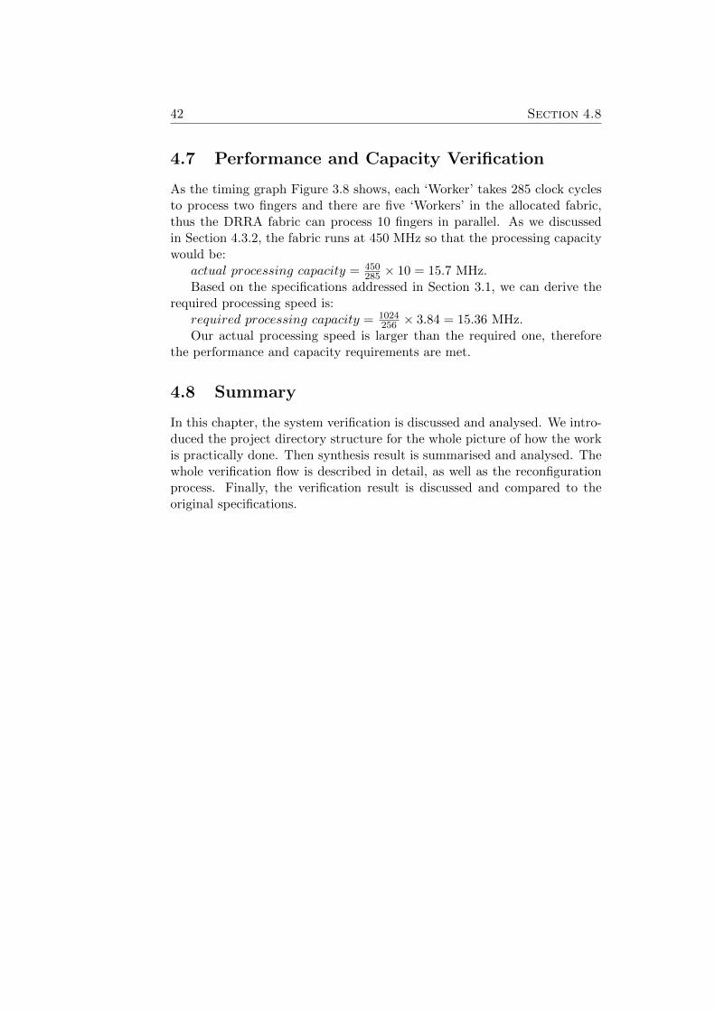
4.7 Performance and Capacity Verification
As the timing graph Figure 3.8 shows, each ‘Worker’ takes 285 clock cyclesto process two fingers and there are five ‘Workers’ in the allocated fabric,thus the DRRA fabric can process 10 fingers in parallel. As we discussedin Section 4.3.2, the fabric runs at 450 MHz so that the processing capacitywould be:
actual processing capacity = 450285 × 10 = 15.7 MHz.
Based on the specifications addressed in Section 3.1, we can derive therequired processing speed is:
required processing capacity = 1024256 × 3.84 = 15.36 MHz.
Our actual processing speed is larger than the required one, thereforethe performance and capacity requirements are met.
4.8 Summary
In this chapter, the system verification is discussed and analysed. We intro-duced the project directory structure for the whole picture of how the workis practically done. Then synthesis result is summarised and analysed. Thewhole verification flow is described in detail, as well as the reconfigurationprocess. Finally, the verification result is discussed and compared to theoriginal specifications.
Chapter 5
Conclusion and Future Work
In this thesis, we have designed a control system named “Correlation Pool”for the signal spreading in WCDMA. It is implemented on the platformnamed Dynamically Reconfigurable Resource Array (DRRA), which is de-veloped at the School of Information and Communication Technology, RoyalInstitute of Technology (KTH).
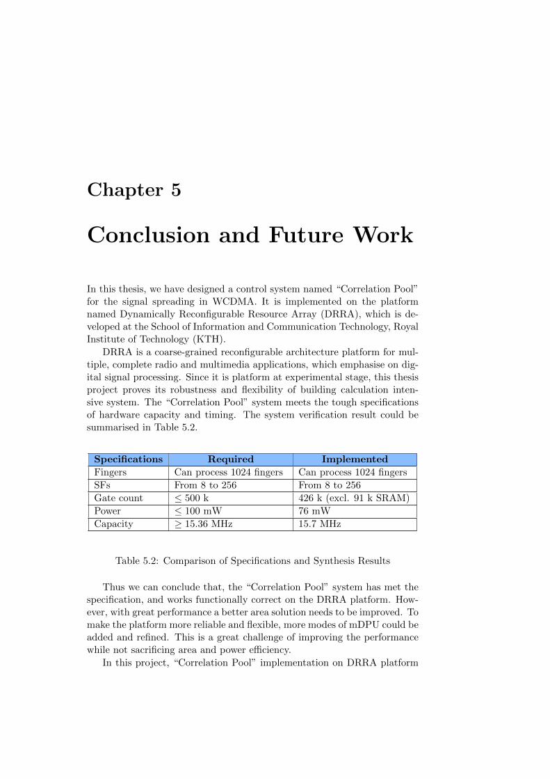
DRRA is a coarse-grained reconfigurable architecture platform for mul-tiple, complete radio and multimedia applications, which emphasise on dig-ital signal processing. Since it is platform at experimental stage, this thesisproject proves its robustness and flexibility of building calculation inten-sive system. The “Correlation Pool” system meets the tough specificationsof hardware capacity and timing. The system verification result could besummarised in Table 5.2.
Specifications Required Implemented
Fingers Can process 1024 fingers Can process 1024 fingers
SFs From 8 to 256 From 8 to 256
Gate count ≤ 500 k 426 k (excl. 91 k SRAM)
Power ≤ 100 mW 76 mW
Capacity ≥ 15.36 MHz 15.7 MHz
Table 5.2: Comparison of Specifications and Synthesis Results
Thus we can conclude that, the “Correlation Pool” system has met thespecification, and works functionally correct on the DRRA platform. How-ever, with great performance a better area solution needs to be improved. Tomake the platform more reliable and flexible, more modes of mDPU could beadded and refined. This is a great challenge of improving the performancewhile not sacrificing area and power efficiency.
In this project, “Correlation Pool” implementation on DRRA platform

44 Chapter 5
has proved the capability of the platform of achieving calculation intensivemultimedia applications. In the next step, a hierarchical hardware compilercould be developed for the automation of design process. Currently, thesequencer instructions and mDPU modes are still obscure and difficult toremember. When writing a configware, the programmer needs to pay moreattention to the instruction format than the structure of the configware.A more understandable structure of instructions could be improved whendesigning the hierarchical hardware compiler.
The initial objective of next stage is a more flexible and efficient designprocess on DRRA platform could be achieved with the hierarchical hardwarecompiler. In the meanwhile, the performance of the DRRA platform couldalso be improved.
Bibliography
[1] H. Holma and A. Toskala, “WCDMA for UMTS, Third Edition”, 2004.
[2] 3GPP TS 25.213 V9.2.0, 2010-09, “3rd Generation Partnership Project;Technical Specification Group Radio Access Network; Spreading andmodulation (FDD) (Release 9)”.
[3] A. Hemani, DRRA Summary, 2009.
[4] S. Li and G. Chen, “A Code Reuse Method for Many-Core Coarse-Grained Reconfigurable Architecture Function Library Development”,2011.
[5] N. Farahini, “An Improved Hierarchical Design Flow for Coarse GrainRegular Fabric”, 2011.
[6] M. Shami and A. Hemani, “An Improved Self-reconfigurable Intercon-nection Scheme for a Coarse Grain Reconfigurable Architecture,” inNORCHIP, 2010, nov. 2010, pp. 1 - 6.
[7] S. Kim, M. Kim, C. Shin, J. Lee, and Y. Kim, “Efficient Implemen-tation of OVSF Code Generator for UMTS Systems” presented at theIEEE Pacific Rim Conference on Communications, Computers and Sig-nal Processing, 2009.
[8] H. Giefers and M. Platzner, “Armlang: A Language and Compilerfor Programming Reconfigurable Mesh Many-cores,” in Parallel Dis-tributed Processing, 2009. IPDPS 2009. IEEE International Sympo-sium, on May, 2009, pp. 1 - 8.
[9] O. Malik, A. Hemani, and M. Shami, “A Library Development Frame-work for A Coarse Grain Reconfigurable Architecture”, in VLSI Design(VLSI Design), 2011 24th International Conference, on Jan, 2011, pp.153 - 158.


Appendix A
Sequencer Instructions
RFILE1
Descriptions: This instruction describes the linear operations of registerfiles. This is the first part if no repetitions needed.
Instruction words Length Description
instruction code 4 Fixed value rfileinstr = 1 indi-cating it as register file instruction.
rf port 2 Specifies which register file port is be-ing operated, read or write.RA=2, RB=3, WA=0, WB=1.
rf valid 1 Determines whether the register file ifvalid or not. Usually it is set to 1.
mode 1 Always set to linear = 1 for linearmode.
start address 6 Indicates the starting address for read-ing/writing data (0-63).
num of addr 6 Indicates how many data should beread/written in register files.
incr 1 Specifies incrementally/decrementallyread/write operations.+ = increment(1), - = decrement(0).
incr value 5 Indicates the incremental or decremen-tal value.
initial delay 6 Specifies the initial delay (cycles) of ex-ecuting this instruction.
output control 2 Specifies which direction the data is go-ing. Only valid for outputs.3=both direction, 2=left, 1=right,0=output 0.

II Appendix A
complete 1 Indicates whether the register file in-struction needs extended second part.NO=0, YES=1.
abnormal 1 Specifies the reading/writing opera-tions should be done infinitely or not.NO=0, YES=1.
Example:
RFILE1 rfileinstr RA 1 linear 0 7 + 1 2 3 YES NO;
This instruction reads the current sequencer’s register file from port A, inlinear mode. It starts to read at address 0, the next address is 1, and soforth, read 8 data, to both directions of output. This instruction is executed2 cycles later after it is queued in the sequencer. This read operation needsonly part 1, stops after it finishes reading 8 data, and the output will returnto 0.
The operations are:RA0, RA1, RA2, RA3, RA4, RA5, RA6, RA7, STOP.
Notes:
The instruction words: start address, num of addr, incr value, andinitial delay, could be configured by INDIRECT instruction, to makeRFILE1 to work in ‘indirect’ mode. These words could be specified fromOUT0 or OUT1 or both, from the mDPU in the same DRRA cell. Thusin ’indirect’ mode, no matter what values are specified in RFILE1, theinstruction will ignore them and take the values from those ports.

Appendix A III
RFILE2
Descriptions: This instruction describes the linear operations of registerfiles. This is the second part for extended repetition operations. It repeatsthe specified times of operations in RFILE1. Can only be used after anRFILE1 instruction whose complete word is set NO.
Instruction words Length Description
instruction code 4 Fixed value rfileinstr = 1 indi-cating it as register file instructions.
rpt delay 6 Specifies the delay (cycles) betweentwo repetitions of RFILE1.
num of rpt 6 Number of repetitions of RFILE1 op-erations.
rpt incr value 6 Specifies the incremented value of nextstarting address.
middle delay 7 Specifies the delay between two consec-utive data being read/written.
add sub 1 A control word reserved for FFT (FastFourier Transformation) mode. Set to0 for linear mode.
skip point 1 A control word reserved for FFT mode.Set to 0 for linear mode.
FFT stage 1 A control word reserved for FFT mode.Set to 0 for linear mode.
initial point 1 A control word reserved for FFT mode.Set to 0 for linear mode.
Example:
RFILE1 rfileinstr RA 1 linear 0 3 + 1 0 3 NO NO;RFILE2 rfileinstr 1 1 1 0 0 0 0 0;
This instruction reads the current sequencer’s register file from port A, inlinear mode. It starts to read at address 0, the next address is 1, and soforth, read 4 data, to both directions of output. The repetition delay is 1,thus after reading 4 data, the register file will wait 1 cycles and then start toread another 4 data. The num of rpt is set to be 1, thus it will repeat once.And the rpt incr value is set to 1, thus in the next starting address isincremented by 1. No middle delay is specified.
The operations are:RA0, RA1, RA2, RA3, WAIT, RA1, RA2, RA3, RA4, STOP.
IV Appendix A
Notes:
The instruction words: rpt delay, num of rpt, rpt incr value, andmiddle delay, could be configured by INDIRECT instruction, to makeRFILE2 to work in ‘indirect’ mode. These words could be specified fromOUT0 or OUT1 or both, from the mDPU in the same DRRA cell. Thusin ’indirect’ mode, no matter what values are specified in RFILE2, theinstruction will ignore them and take the values from those ports.

Appendix A V
INDIRECT
Descriptions: This instruction sets the register file operations to ‘indi-rect’ mode. It configures the sources of the specified words in RFILE1 andRFILE2 instructions. It can only be placed before RFILE1 instruction.
Instruction words Length Description
instruction code 4 Fixed value idinstr = 8 indicat-ing it as register file indirect configu-ration instructions.
start addr src 2 Specifies the source of thestart address word in thefollowing RFILE1 instruction.(OUT0=2, OUT1=1, BOTH=3,NONE=0.)
num of addr src 2 Specifies the source of thenum of addr word in the fol-lowing RFILE1 instruction.(OUT0=2, OUT1=1, BOTH=3,NONE=0.)
incr value src 2 Specifies the source of theincr value word in the fol-lowing RFILE1 instruction.(OUT0=2, OUT1=1, BOTH=3,NONE=0.)
initial delay src 2 Specifies the source of theinitial delay word in thefollowing RFILE1 instruction.(OUT0=2, OUT1=1, BOTH=3,NONE=0.)
rpt delay src 2 Specifies the source of therpt delay word in the follow-ing RFILE2 instruction.(OUT0=2, OUT1=1, BOTH=3,NONE=0.)
num of rpt src 2 Specifies the source of thenum of rpt word in the follow-ing RFILE2 instruction.(OUT0=2, OUT1=1, BOTH=3,NONE=0.)

VI Appendix A
rpt incr value src 2 Specifies the source of therpt incr value word in thefollowing RFILE2 instruction.(OUT0=2, OUT1=1, BOTH=3,NONE=0.)
middle delay src 2 Specifies the source of themiddle delay word in the fol-lowing RFILE2 instruction.(OUT0=2, OUT1=1, BOTH=3,NONE=0.)
idinstr unused 16 16 unused bits, set to 0.
Example:
INDIRECT idinstr OUT0 0 0 0 0 0 0 0 0;RFILE1 rfileinstr RA 1 linear 0 3 + 1 0 3 NO NO;RFILE2 rfileinstr 1 1 1 0 0 0 0 0;
These instructions read the current sequencer’s register file from port A, inlinear mode. It starts to read at address which is given from OUT0 of mDPU,for example, if it is 4, the next address is 5, and so forth, read 4 data, toboth directions of output. This instruction is executed immediately after itis queued in the sequencer. The read operation will be repeated once after1 cycle, starting from the the previous start address + 1, read 4 dataand stops.
The operations are:RA4, RA5, RA6, RA7, WAIT, RA5, RA6, RA7, RA8, STOP.
Notes:
If the sources of instruction words are specified, the sources have higher pri-orities, even if those words are specified in the following RFILE1 or RFILE2instructions.

Appendix A VII
MDPU
Descriptions: This instruction describes operations of mDPU.
Instruction words Length Description
instruction code 4 Fixed value mdpuinstr = 2 indicat-ing it as mDPU instructions.
mpdu mode 5 Specifies which mode the currentDRRA cell’s mDPU is operating.
mdpu unused 9 9 9 unused bits for mDPU, set to 0 whenusing MDPU.
reserved 5 5 Reserved 5 bits for further functional-ity, set to 0 when using MDPU.
output ctrl 0 2 Specifies which direction the data fromoutput 0 is going.3=both direction, 2=left, 1=right,0=output 0.
output ctrl 1 2 Specifies which direction the data fromoutput 1 is going.3=both direction, 2=left, 1=right,0=output 0.
reserved 8 Reserved 8 bits for further functional-ity, set to 0 when using MDPU.
mdpu unused 1 1 1 unused bits for mDPU, set to 0 whenusing MDPU.
Example:
MDPU mdpuinstr 2 0 0 3 3 0 0;
This instruction makes the mDPU work in mode 2, which is asymmetricFIR MAC with internal accumulation (out3 = in0× in2, out2 = in0×in2 + acc (acc is the internal accumulator)).
Notes:
The mDPUs will keep the current mode until being set to another mode.Refer to Appendix B for more details about mDPU modes.

VIII Appendix A
CONSTANT
Descriptions: This instruction sets the constants value of mDPUs.
Instruction words Length Description
instruction code 4 Fixed value constinstr = 3 indi-cating it as CONSTANT instruction.
constant value 1 16 Specifies the value of constant 1.
constant value 2 16 Specifies the value of constant 2.
Example:
CONSTANT constinstr 2 4;
This instruction sets the value of const1 of mDPU to 2, and the value ofconst2 to 4.

Appendix A IX
DELAY
Descriptions: This instruction makes current sequencer delay specifiedcycles.
Instruction words Length Description
instruction code 4 Fixed value delayinstr = 13 indi-cating it as DELAY instruction.
cycles 15 Specifies the number of cycles intendedto be delayed.(actual number - 1).
delay unused 17 17 unused bits for instruction DELAY.
Example:
DELAY delayinstr 3 0;
This instruction will make the current sequencer take empty operations for3 cycles.
Notes:
In fact, ‘DELAY’ instruction itself will take 1 cycle, thus after executing thisinstruction, the actual delay cycles will plus 1. In the example, for theperspective of users, executing the instruction actually delay 4 cycles.

X Appendix A
CONNECT
Descriptions: This instruction is used for establishing connections betweenregister files and mDPUs.
Instruction words Description
cnt obj a Connection object A.The keywords could either be ‘REFI’ for registerfiles, or ‘DPU’ for mDPUs.
obj addr a Specifies the connection object A’s address (theSquencener Indices).
port keyworkd a Keyword for port type.Port type could either be ‘OUT’ or ‘IN’.
port num a Specifies which port the object is using for con-nection. For ‘OUT’, it could either be 0 or 1; For‘IN’, it could be 0, 1, 2, 3.
to Keyword ‘TO’.
cnt obj b Connection object B.The keywords could either be ‘REFI’ for registerfiles, or ‘DPU’ for mDPUs.
obj addr b Specifies the connection object B’s address (theSquencener Indices).
port keyworkd b Keyword for port type.Port type could either be ‘OUT’ or ‘IN’.
port num b Specifies which port the object is using for con-nection. For ‘OUT’, it could either be 0 or 1; For‘IN’, it could be 0, 1, 2, 3.
Example:
CONNECT REFI 4 OUT 0 TO DPU 0 IN 0;
This instruction connects port A of register file with index 4 to the input 0of mDPU with index 0.
Notes:
For register files, the port keyword can always be OUT, and port numberis 0 or 1, indicating their port A or port B. Also pay attention to theconnectivity between DRRA cells.

Appendix A XI
HCOUT
Descriptions: This instruction makes the sequencer sends out HierarchicalControl signals.
Instruction words Length Description
instruction code 4 Fixed value send = 6 indicating it asHCOUT instruction.
src constant 1 Specifies the source of the HC signal isfrom the specified constant or not. Setto ‘0’ if not, otherwise set to ‘1’. If setto ‘1’, the word const value shouldbe specified.
src RA 1 Specifies the source of the HC signal isfrom the the current cell’s register file’soutput port A or not. Set to ‘0’ if not,otherwise set to ‘1’.
src RB 1 Specifies the source of the HC signal isfrom the the current cell’s register file’soutput port B or not. Set to ‘0’ if not,otherwise set to ‘1’.
src O0 1 Specifies the source of the HC signalis from the the current cell’s mDPU’soutput 0 or not. Set to ‘0’ if not, oth-erwise set to ‘1’.
src O1 1 Specifies the source of the HC signalis from the the current cell’s mDPU’soutput 1 or not. Set to ‘0’ if not, oth-erwise set to ‘1’.
const value 4 Specifies the constant value (0-15)which is sent. It will be sent when theword src constant is set to 1.
hc unused 23 23 unused bits for HCOUT instruction.
Example:
HCOUT send 1 0 0 0 0 12;
This instruction will make the sequencer send out Hierarchical Control signal‘12’ using specified constant.

XII Appendix A
HCBR
Descriptions: This instruction makes the sequencer wait on HierarchicalSignals from source sequencers for comparison to jump to different branches.
Instruction words Length Description
instruction code 4 Fixed value wait = 5 indicating it asHCBR instruction.
src seq 4 Specifies the source sequencer whichsends the hierarchical control signal.
compare value 4 Specifies the comparison value which iscompared to the signal from the sourcesequencer.
true address 7 The branch address (label) when thecomparison result is true.
false address 7 The branch address (label) when thecomparison result is false.
go false 1 Specifies whether the instruction willjump to the false address whenthe comparison is false. Normally setto 1.
hcbr unused 9 9 unused bits for HCBR instruction.
Example:
HCBR wait 1 12 TrueAddr FalseAddr 1 0;
This instruction will make the sequencer wait until it receives an HC signalfrom sequencer 1. Then it will compare the received signal to 12, if it isequal to 12, then jump to branch with label ‘TrueAddr’, otherwise jumpto the branch with label ‘FalseAddr’.
Notes:
Pay attention to the connectivity between DRRA cells. A DRRA cell canonly communicate with other DRRA cells within the local connectivity area.

Appendix A XIII
HCWAIT
Descriptions: This instruction makes the sequencer wait until it receivesthe expected signals from the specified source sequencer.
Instruction words Length Description
instruction code 4 Fixed value wait = 5 indicating it asHCWAIT instruction.
src seq 4 Specifies the source sequencer whichsends the hierarchical control signal.
compare value 4 Specifies the comparison value which iscompared to the signal from the sourcesequencer.
true address 7 The branch address (label) when thecomparison result is true.
hcwait unused 17 17 unused bits for HCWAIT instruction.
Example:
HCWAIT wait 1 12 Continue 0;
This instruction will make the sequencer wait until it receives the Hierarchi-cal Control signal from sequencer 1. Then it compares the received signal to12. If it is equal to 12, then jumps to the branch with the label ‘Continue’,otherwise the sequencer still waits.
Notes:
Pay attention to the connectivity between DRRA cells. A DRRA cell canonly communicate with other DRRA cells within the local connectivity area.
The HCWAIT instruction is actually a variation of simplified instructionHCBR. Since they use the same hardware, they have same instruction code.

XIV Appendix A
JUMP
Descriptions: This instruction makes the sequencer unconditionally jumpto the specified labelled branch.
Instruction words Length Description
instruction code 4 Fixed value tothe = 5 indicating itas JUMP instruction.
status 11 Mask bits for hardware, set to the key-word address for setting all the 11bits 0.
true address 7 The branch address (label) where thesequencer shall unconditionally jump.
jump unused 14 14 unused bits for JUMP instruction.
Example:
JUMP tothe address Start 0;
The sequencer will unconditionally jump to the address labelled ‘Start’.
Notes:
Pay attention to the connectivity between DRRA cells. A DRRA cell canonly communicate with other DRRA cells within the local connectivity area.
The JUMP instruction is actually a variation of simplified instructionHCBR. Since they use the same hardware, they have same instruction code.

Appendix B
mDPU Modes
Note: In this appendix we only include the mDPU modes involved incorrelation pool implementation in DRRA.
Mode 6 m SRL inDescription In this mode, mDPU takes the data from the input port as
the scrambling code generator polynomial configuration forthe lower 16 bits of the long scrambling code clong,1,n, andputs it in the corresponding scrambling register.
Mode 7 m SRH inDescription In this mode, mDPU takes the data from the input port as
the scrambling code generator polynomial configuration forthe higher 7 bits of the long scrambling code clong,1,n, andputs it in the corresponding scrambling register.
Mode 8 m SIL inDescription In this mode, mDPU takes the data from the input port as
the scrambling code generator polynomial configuration forthe lower 16 bits of the long scrambling code clong,2,n, andputs it in the corresponding scrambling register.
Mode 26 m SIH inDescription In this mode, mDPU takes the data from the input port as
the scrambling code generator polynomial configuration forthe higher 7 bits of the long scrambling code clong,2,n, andputs it in the corresponding scrambling register.
Mode 27 m UID inDescription In this mode, mDPU takes the data from the input port
as the user ID, and puts it in the corresponding user-IDregister.
Mode 28 m OVSF idx in

XVI Appendix B
Description In this mode, mDPU takes the data from the input portas the OVSF index configuration, and puts it in the corre-sponding OVSF index configuration register.
Mode 9 m cgDescription In this mode, mDPU works in the code generation mode.
It produces the correlation codes according to the configu-ration.
Mode 10 m vec rotDescription In this mode, mDPU works in the vector rotation mode.
It correlates the input sample with the correlation codesproduced by another mDPU.
Output out0 = in0× in2 + acc0;out1 = in1× in3 + acc1,where in0 and in1 are sample data, in2 and in3 arecorrelation codes, and acc0 and acc1 are internal accu-mulators.
Mode 17 m bypassDescription In this mode, mDPU simply puts the input values to the
output ports. This operation introduces one cycle delay.
Output out0 = in0;out1 = in1.
Mode 20 m SRL outDescription In this mode, mDPU reads out its scrambling code register
for lower 16 bit for long scrambling code clong,1,n and putsthe result to outputs.
Mode 22 m SRH outDescription In this mode, mDPU reads out its scrambling code register
for higher 7 bit for long scrambling code clong,1,n and putsthe result to outputs.
Mode 21 m SIL outDescription In this mode, mDPU reads out its scrambling code register
for lower 16 bit for long scrambling code clong,2,n and putsthe result to outputs.
Mode 23 m SIH outDescription In this mode, mDPU reads out its scrambling code register
for higher 7 bit for long scrambling code clong,2,n and putsthe result to outputs.
Mode 24 m UID outDescription In this mode, mDPU reads out its user-ID register and puts
the result to outputs.

Appendix C
Configwares for CorrelationPool Algorithm
C.1 Definitions of Global Constants
0 /* Global Constants */12 /* Global Hierarchical Control Signals */3 #DEFINE CONST act 8;4 #DEFINE CONST idle 10;5 #DEFINE CONST busy 12;67 /* SRAM to bus then to refi */8 /* bus is 16-bit wide */9 /* 16 * 12 = 192 cycles < 256 */
10 #DEFINE CONST seq_initial_dly 255;11 /* code_gen_dly = Spreading Factor - 2 */12 #DEFINE CONST code_gen_dly 254;1314 /* Predicatable Delays */15 #DEFINE CONST code_dly 4;16 #DEFINE CONST finger_0_dly 8;17 #DEFINE CONST finger_1_dly 5;18 #DEFINE CONST send_cfg_dly 8;1920 /* REFI_range = SMALL(SF-1, 63) */21 #DEFINE CONST REFI_range 63;22 /* REFI_rpt = floor(SF/REFI_range) - 1 */23 #DEFINE CONST REFI_rpt 3;2425 /* mDPU modes */26 #DEFINE CONST m_SRL_in 6;27 #DEFINE CONST m_SRH_in 7;28 #DEFINE CONST m_SIL_in 8;29 #DEFINE CONST m_CG 9;30 #DEFINE CONST m_vec_rot 10;31 #DEFINE CONST m_bypass 17;

XVIII Appendix C
32 #DEFINE CONST m_SIH_in 26;33 #DEFINE CONST m_UID_in 27;34 #DEFINE CONST m_OVSF_idx_in 28;35 #DEFINE CONST m_SRL_out 20;36 #DEFINE CONST m_SRH_out 22;37 #DEFINE CONST m_SIL_out 21;38 #DEFINE CONST m_SIH_out 23;39 #DEFINE CONST m_UID_out 24;

Appendix C XIX
C.2 Configware for Controller
0 USE SEQ 111 /* Sequencer (1,2) Controller */23 #DEFINE CONST work_0 1;4 #DEFINE CONST work_1 3;5 #DEFINE CONST work_2 5;6 #DEFINE CONST work_3 7;7 #DEFINE CONST work_4 9;89 #DEFINE CONST worker_loc_0 1;
10 #DEFINE CONST worker_loc_1 3;11 #DEFINE CONST worker_loc_2 7;12 #DEFINE CONST worker_loc_3 9;13 #DEFINE CONST worker_loc_4 11;14 #DEFINE CONST stimuli_loc 4;15 #DEFINE CONST self_loc 5;1617 #DEFINE CONST finger_cfg_dly 5;18 #DEFINE CONST cfg_in_dly 99;19 #DEFINE CONST seq_initial_dly 255;2021 DELAY delayinstr seq_initial_dly 0;2223 CONNECT REFI stimuli_loc OUT 0 TO DPU self_loc IN 0;24 CONNECT REFI stimuli_loc OUT 1 TO DPU self_loc IN 1;2526 MDPU mdpuinstr m_bypass 0 0 3 3 0 0;2728 /Start/ HCOUT send 1 0 0 0 0 idle 0;29 HCWAIT wait stimuli_loc act Chk_0 0;3031 /Chk_0/ HCBR wait worker_loc_0 idle Get_cfg_0 Chk_1 1 0;32 /Chk_1/ HCBR wait worker_loc_1 idle Get_cfg_1 Chk_2 1 0;33 /Chk_2/ HCBR wait worker_loc_2 idle Get_cfg_2 Chk_3 1 0;34 /Chk_3/ HCBR wait worker_loc_3 idle Get_cfg_3 Chk_4 1 0;35 /Chk_4/ HCBR wait worker_loc_4 idle Get_cfg_4 Chk_0 1 0;3637 /Get_cfg_0/ HCOUT send 1 0 0 0 0 busy 0;38 HCOUT send 1 0 0 0 0 work_0 0;39 JUMP tothe address End 0;4041 /Get_cfg_1/ HCOUT send 1 0 0 0 0 busy 0;42 HCOUT send 1 0 0 0 0 work_1 0;43 JUMP tothe address End 0;4445 /Get_cfg_2/ HCOUT send 1 0 0 0 0 busy 0;46 HCOUT send 1 0 0 0 0 work_2 0;47 JUMP tothe address End 0;4849 /Get_cfg_3/ HCOUT send 1 0 0 0 0 busy 0;50 HCOUT send 1 0 0 0 0 work_3 0;

XX Appendix C
51 JUMP tothe address End 0;5253 /Get_cfg_4/ HCOUT send 1 0 0 0 0 busy 0;54 HCOUT send 1 0 0 0 0 work_4 0;5556 /End/ DELAY delayinstr send_cfg_dly 0;57 JUMP tothe address Start 0;

Appendix C XXI
C.3 Configware for Stimuli
0 /* Stimuli for 7 finger(s) */12 USE SEQ 934 #DEFINE CONST controller 5;56 DELAY delayinstr seq_initial_dly 0;78 /Send_0/ HCWAIT wait controller idle Act_0 0;9
10 /Act_0/ HCOUT send 1 0 0 0 0 act 0;11 HCWAIT wait controller busy Send_cfg_0 0;1213 /Send_cfg_0/ HCOUT send 1 0 0 0 0 busy 0;14 RFILE1 rfileinstr RA 1 linear 0 6 + 1 3 3 YES NO;15 RFILE1 rfileinstr RB 1 linear 0 6 + 1 2 3 YES NO;16 DELAY delayinstr send_cfg_dly 0;1718 /Send_1/ HCWAIT wait controller idle Act_1 0;1920 /Act_1/ HCOUT send 1 0 0 0 0 act 0;21 HCWAIT wait controller busy Send_cfg_1 0;2223 /Send_cfg_1/ HCOUT send 1 0 0 0 0 busy 0;24 RFILE1 rfileinstr RA 1 linear 7 6 + 1 3 3 YES NO;25 RFILE1 rfileinstr RB 1 linear 7 6 + 1 2 3 YES NO;26 DELAY delayinstr send_cfg_dly 0;2728 /Send_2/ HCWAIT wait controller idle Act_2 0;2930 /Act_2/ HCOUT send 1 0 0 0 0 act 0;31 HCWAIT wait controller busy Send_cfg_2 0;3233 /Send_cfg_2/ HCOUT send 1 0 0 0 0 busy 0;34 RFILE1 rfileinstr RA 1 linear 14 6 + 1 3 3 YES NO;35 RFILE1 rfileinstr RB 1 linear 14 6 + 1 2 3 YES NO;36 DELAY delayinstr send_cfg_dly 0;3738 /Send_3/ HCWAIT wait controller idle Act_3 0;3940 /Act_3/ HCOUT send 1 0 0 0 0 act 0;41 HCWAIT wait controller busy Send_cfg_3 0;4243 /Send_cfg_3/ HCOUT send 1 0 0 0 0 busy 0;44 RFILE1 rfileinstr RA 1 linear 21 6 + 1 3 3 YES NO;45 RFILE1 rfileinstr RB 1 linear 21 6 + 1 2 3 YES NO;46 DELAY delayinstr send_cfg_dly 0;4748 /Send_4/ HCWAIT wait controller idle Act_4 0;4950 /Act_4/ HCOUT send 1 0 0 0 0 act 0;
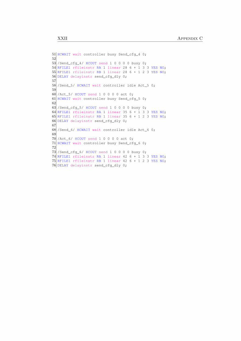
XXII Appendix C
51 HCWAIT wait controller busy Send_cfg_4 0;5253 /Send_cfg_4/ HCOUT send 1 0 0 0 0 busy 0;54 RFILE1 rfileinstr RA 1 linear 28 6 + 1 3 3 YES NO;55 RFILE1 rfileinstr RB 1 linear 28 6 + 1 2 3 YES NO;56 DELAY delayinstr send_cfg_dly 0;5758 /Send_5/ HCWAIT wait controller idle Act_5 0;5960 /Act_5/ HCOUT send 1 0 0 0 0 act 0;61 HCWAIT wait controller busy Send_cfg_5 0;6263 /Send_cfg_5/ HCOUT send 1 0 0 0 0 busy 0;64 RFILE1 rfileinstr RA 1 linear 35 6 + 1 3 3 YES NO;65 RFILE1 rfileinstr RB 1 linear 35 6 + 1 2 3 YES NO;66 DELAY delayinstr send_cfg_dly 0;6768 /Send_6/ HCWAIT wait controller idle Act_6 0;6970 /Act_6/ HCOUT send 1 0 0 0 0 act 0;71 HCWAIT wait controller busy Send_cfg_6 0;7273 /Send_cfg_6/ HCOUT send 1 0 0 0 0 busy 0;74 RFILE1 rfileinstr RA 1 linear 42 6 + 1 3 3 YES NO;75 RFILE1 rfileinstr RB 1 linear 42 6 + 1 2 3 YES NO;76 DELAY delayinstr send_cfg_dly 0;

Appendix C XXIII
C.4 Configware for Worker (MAC)
0 USE SEQ 11 /* Sequencer (0,0) MAC 0 */2 #DEFINE CONST work 1;34 #DEFINE CONST controller_loc 5;5 #DEFINE CONST self_loc 0;6 #DEFINE CONST code_loc 1;78 /* Wait for register files ready */9 DELAY delayinstr seq_initial_dly 0;
1011 /Start/ MDPU mdpuinstr m_bypass 0 0 3 3 0 0;1213 HCOUT send 1 0 0 0 0 idle 0;14 HCWAIT wait controller_loc work MAC_work 0;1516 /MAC_work/ HCOUT send 1 0 0 0 0 busy 0;1718 CONNECT DPU controller_loc OUT 0 TO DPU self_loc IN 0;19 CONNECT DPU controller_loc OUT 1 TO DPU self_loc IN 1;2021 DELAY delayinstr 0 0;2223 INDIRECT idinstr OUT0 0 0 0 0 0 0 0 0;24 RFILE1 rfileinstr RA 1 linear 0 REFI_range + 1 finger_0_dly 3 NO
NO;25 RFILE2 rfileinstr 0 REFI_rpt 0 0 0 0 0 0;2627 INDIRECT idinstr OUT1 0 0 0 0 0 0 0 0;28 RFILE1 rfileinstr RB 1 linear 0 REFI_range + 1 finger_1_dly 3 NO
NO;29 RFILE2 rfileinstr 0 REFI_rpt 0 0 0 0 0 0;3031 CONNECT DPU code_loc OUT 0 TO DPU self_loc IN 2;32 CONNECT DPU code_loc OUT 1 TO DPU self_loc IN 3;3334 CONNECT REFI self_loc OUT 0 TO DPU self_loc IN 0;35 CONNECT REFI self_loc OUT 1 TO DPU self_loc IN 1;3637 DELAY delayinstr 0 0;3839 MDPU mdpuinstr m_vec_rot 0 0 3 3 0 0;40 DELAY delayinstr code_gen_dly 0;4142 /**dly for waitng code generator **/43 DELAY delayinstr code_dly 0;4445 JUMP tothe address Start 0;

XXIV Appendix C
C.5 Configware for Worker (Code Generator)
0 USE SEQ 31 /* Sequencer (1,0) CG 0 */23 #DEFINE CONST work 1;45 #DEFINE CONST controller_loc 5;6 #DEFINE CONST self_loc 1;78 CONNECT DPU controller_loc OUT 0 TO DPU self_loc IN 1;9 CONNECT DPU controller_loc OUT 1 TO DPU self_loc IN 3;
1011 /Start/ MDPU mdpuinstr m_bypass 0 0 0 0 0 0;1213 HCOUT send 1 0 0 0 0 idle 0;14 HCWAIT wait controller_loc work Read_cfg_in 0;1516 /Read_cfg_in/ HCOUT send 1 0 0 0 0 busy 0;17 DELAY delayinstr 5 0;1819 /* receive finger configuration */20 MDPU mdpuinstr m_UID_in 0 0 0 0 0 0;21 MDPU mdpuinstr m_OVSF_idx_in 0 0 0 0 0 0;22 MDPU mdpuinstr m_SRL_in 0 0 0 0 0 0;23 MDPU mdpuinstr m_SRH_in 0 0 0 0 0 0;24 MDPU mdpuinstr m_SIL_in 0 0 0 0 0 0;25 MDPU mdpuinstr m_SIH_in 0 0 0 0 0 0;2627 /* bypass mode added for adding 1 cycle delay */28 MDPU mdpuinstr m_bypass 0 0 0 0 0 0;29 MDPU mdpuinstr m_CG 0 0 3 3 0 0;30 DELAY delayinstr code_gen_dly 0;3132 MDPU mdpuinstr m_UID_out 0 0 3 3 0 0;33 MDPU mdpuinstr m_SRL_out 0 0 3 3 0 0;34 MDPU mdpuinstr m_SRH_out 0 0 3 3 0 0;35 MDPU mdpuinstr m_SIL_out 0 0 3 3 0 0;36 MDPU mdpuinstr m_SIH_out 0 0 3 3 0 0;3738 /* manual delay for 1 cycle */39 MDPU mdpuinstr m_bypass 0 0 0 0 0 0;4041 JUMP tothe address Start 0;