
IMPLEMENTATION OF ARITHMETIC AND LOGICAL UNIT … oct ijamte - 1140.pdfIMPLEMENTATION OF ARITHMETIC...
9
IMPLEMENTATION OF ARITHMETIC AND LOGICAL UNIT THROUGH FINFET Dr. R. Prakash Rao Associate Professor, ECE Department, Matrusri Engineering College, Saidabad, Hyderabad. India. [email protected] ABSTRACT-The FinFET is a novel device structure used in nanometer regime where the conventional CMOS technology’s performance is week due to increased short channel effects (SCEs). Double-gate (DG) FinFET has better SCEs performance compares to conventional CMOS. The maximum drain current produces by dual gate mode is much higher than single gate mode. A 1-bit ALU has been designed using MOSFET and FinFET and simulated, which implements four basic operations like addition, subtraction, AND,OR. All the results are carried out using H-spice simulation tool. The simulation of ALU is carried at 32nm technology. The results obtained from simulation of FinFET ALU are compared with conventional MOS ALU. The figure of merit measured for ALU are power and delay. The power in FinFET was found out to be 85 % less than the MOS ALU. The delay of ALU was found to be 93 % less than MOS ALU. KEYWORDS- FinFET, CMOS, ITRS, Short channel effects (SCEs), Circuit Design, Device simulation, ALU, H-spice. I. INTRODUCTION The integrated chip technology has revolutionized the world of electronics in which MOS transistors have played a vital role in enhancing performance of integrated devices. In order to achieve high density and performance, MOS devices are continuously being scaled from last two decades. The ITRS has proposed multi-gate field-effect transistors (FETs) such as planar double-gate FETs and FinFETs as a possible scaling path for low power digital CMOS technologies[1]. The difficulties in shrinking the size of traditional bulk transistor give rise to the development of a new device architecture in which two gates, one on each side of the body, are used per device[2]. Although early double- gate faced manufacturing challenges associated with vertical structure more recently, double-gate devices called FinFET or wrap around FETs that are compatible with standard CMOS[3]. FinFET offers distinct advantages for scaling to very short gate lengths. Fabrication of FinFET is similar to that of conventional MOSFETs and holds a grater similarities with SOI devices[4]. These devices could be more beneficial than three terminal devices since the Threshold voltages can be adjusted by biasing the back gate terminal which tends to reduce sub-threshold leakage current and improve the slope factor[10]. The advantage of FinFET technology are higher drain current and switching speed, less than half the dynamic power requirement less static leakage current[8]-[9]. The channel of finFET is a fin of undoped silicon perpendicular to the substrate. At least two sides of the fin are wrapped around by oxide simultaneously, which breakup the active regions into several fins resulting the increased electrostatic control of the gate over the channel makes very high Ion/Ioff ratios achievable [3]. The most important geometric parameters of a FinFET are its fin height (Hfin), fin-width (Wfin) and gate length Lg[9]. II. FINFET TECHNOLOGY OVERVIEW The FinFET are quasi-planar field-effect transistors. The working principle is same as that of planar MOSFET. FinFET device have lower gate leakage, stronger gate control, and less performance variability compared to bulk CMOS counterparts. A FinFET device has a double gate structure[7], a front gate and back gate as shown in Figure 1. International Journal of Management, Technology And Engineering Volume 8, Issue X, OCTOBER/2018 ISSN NO : 2249-7455 Page No:2863
Transcript of IMPLEMENTATION OF ARITHMETIC AND LOGICAL UNIT … oct ijamte - 1140.pdfIMPLEMENTATION OF ARITHMETIC...

IMPLEMENTATION OF ARITHMETIC AND LOGICAL UNIT THROUGH FINFET
Dr. R. Prakash Rao
Associate Professor, ECE Department, Matrusri Engineering College, Saidabad, Hyderabad. India. [email protected]
ABSTRACT-The FinFET is a novel device structure used in nanometer regime where the conventional CMOS technology’s performance is week due to increased short channel effects (SCEs). Double-gate (DG) FinFET has better SCEs performance compares to conventional CMOS. The maximum drain current produces by dual gate mode is much higher than single gate mode. A 1-bit ALU has been designed using MOSFET and FinFET and simulated, which implements four basic operations like addition, subtraction, AND,OR. All the results are carried out using H-spice simulation tool. The simulation of ALU is carried at 32nm technology. The results obtained from simulation of FinFET ALU are compared with conventional MOS ALU. The figure of merit measured for ALU are power and delay. The power in FinFET was found out to be 85 % less than the MOS ALU. The delay of ALU was found to be 93 % less than MOS ALU. KEYWORDS- FinFET, CMOS, ITRS, Short channel effects (SCEs), Circuit Design, Device simulation, ALU, H-spice.
I. INTRODUCTION
The integrated chip technology has revolutionized the world of electronics in which MOS transistors have played a vital role in enhancing performance of integrated devices. In order to achieve high density and performance, MOS devices are continuously being scaled from last two decades. The ITRS has proposed multi-gate field-effect transistors (FETs) such as planar double-gate FETs and FinFETs as a possible scaling path for low power digital CMOS technologies[1]. The difficulties in shrinking the size of traditional bulk transistor give rise to the development of a new device architecture in which two gates, one on each side of the body, are used per device[2]. Although early double- gate faced manufacturing challenges associated with vertical structure more recently, double-gate devices called FinFET or wrap around FETs that are compatible with standard CMOS[3]. FinFET offers distinct advantages for scaling to very short gate lengths. Fabrication of FinFET is similar to that of conventional MOSFETs and holds a grater similarities with SOI devices[4]. These devices could be more beneficial than three terminal devices since the Threshold voltages can be adjusted by biasing the back gate terminal which tends to reduce sub-threshold leakage current and improve the slope factor[10]. The advantage of FinFET technology are higher drain current and switching speed, less than half the dynamic power requirement less static leakage current[8]-[9]. The channel of finFET is a fin of undoped silicon perpendicular to the substrate. At least two sides of the fin are wrapped around by oxide simultaneously, which breakup the active regions into several fins resulting the increased electrostatic control of the gate over the channel makes very high Ion/Ioff ratios achievable [3]. The most important geometric parameters of a FinFET are its fin height (Hfin), fin-width (Wfin) and gate length Lg[9].
II. FINFET TECHNOLOGY OVERVIEW
The FinFET are quasi-planar field-effect transistors. The working principle is same as that of planar MOSFET. FinFET device have lower gate leakage, stronger gate control, and less performance variability compared to bulk CMOS counterparts. A FinFET device has a double gate structure[7], a front gate and back gate as shown in Figure 1.
International Journal of Management, Technology And Engineering
Volume 8, Issue X, OCTOBER/2018
ISSN NO : 2249-7455
Page No:2863
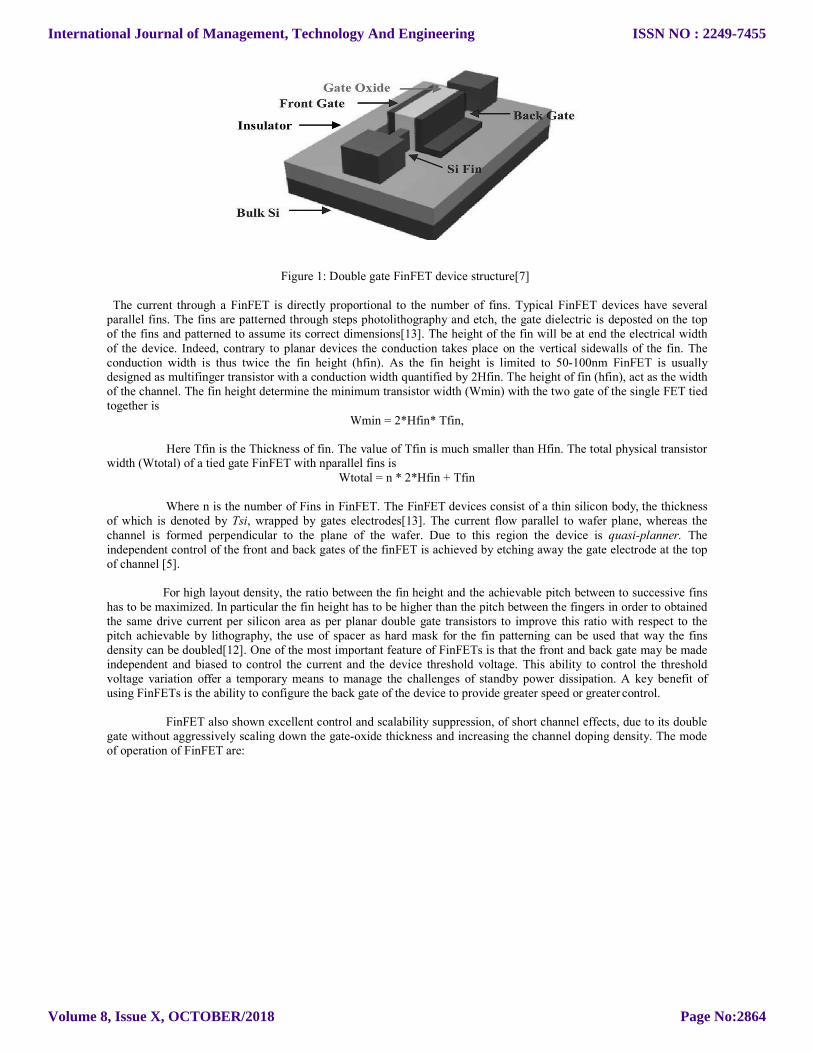
Figure 1: Double gate FinFET device structure[7]
The current through a FinFET is directly proportional to the number of fins. Typical FinFET devices have several parallel fins. The fins are patterned through steps photolithography and etch, the gate dielectric is deposted on the top of the fins and patterned to assume its correct dimensions[13]. The height of the fin will be at end the electrical width of the device. Indeed, contrary to planar devices the conduction takes place on the vertical sidewalls of the fin. The conduction width is thus twice the fin height (hfin). As the fin height is limited to 50-100nm FinFET is usually designed as multifinger transistor with a conduction width quantified by 2Hfin. The height of fin (hfin), act as the width of the channel. The fin height determine the minimum transistor width (Wmin) with the two gate of the single FET tied together is
Wmin = 2*Hfin* Tfin,
Here Tfin is the Thickness of fin. The value of Tfin is much smaller than Hfin. The total physical transistor width (Wtotal) of a tied gate FinFET with nparallel fins is
Wtotal = n * 2*Hfin + Tfin
Where n is the number of Fins in FinFET. The FinFET devices consist of a thin silicon body, the thickness of which is denoted by Tsi, wrapped by gates electrodes[13]. The current flow parallel to wafer plane, whereas the channel is formed perpendicular to the plane of the wafer. Due to this region the device is quasi-planner. The independent control of the front and back gates of the finFET is achieved by etching away the gate electrode at the top of channel [5].
For high layout density, the ratio between the fin height and the achievable pitch between to successive fins
has to be maximized. In particular the fin height has to be higher than the pitch between the fingers in order to obtained the same drive current per silicon area as per planar double gate transistors to improve this ratio with respect to the pitch achievable by lithography, the use of spacer as hard mask for the fin patterning can be used that way the fins density can be doubled[12]. One of the most important feature of FinFETs is that the front and back gate may be made independent and biased to control the current and the device threshold voltage. This ability to control the threshold voltage variation offer a temporary means to manage the challenges of standby power dissipation. A key benefit of using FinFETs is the ability to configure the back gate of the device to provide greater speed or greater control.
FinFET also shown excellent control and scalability suppression, of short channel effects, due to its double
gate without aggressively scaling down the gate-oxide thickness and increasing the channel doping density. The mode of operation of FinFET are:
International Journal of Management, Technology And Engineering
Volume 8, Issue X, OCTOBER/2018
ISSN NO : 2249-7455
Page No:2864

Figure 2: SG-mode NAND[5] Figure 3: IG-mode NAND[5]
Figure 4: LP-mode NAND[5] Figure 5: IG/LP-mode NAND[5]
The Short-gate (SG) mode – In this mode of operation both p-type FinFET and n-type FinFET back gate are
connected its front gate Figure 2, show NAND gate using shorted gate mode. This configuration is best suitable for high performance applications.
The Independent gate (IG) mode – This mode of operation the two gates are electrically independent and provides two different active mode of operation with significantly different current charcterstics determined by the bias conditions[11], the NAND gate schematic in IG mode shown in Figure 3.
The Low power (LP) mode – In this mode of operation back gate is tied to reverse bias voltage to reduce leakage power, the NAND gate in LP mode is shown in Figure 4.
The hybrid (IG/LP) mode – this mode is a combination of LP and IG modes, NAND gate schematic for hybrid mode is shown in Figure 5.
III. DESIGN OF ARITHMATIC LOGIC UNIT (ALU)
Arithmetic and logical unit is a combinational logic unit that performs its arithmetic and logical operations. The design of 1 bit ALU which perform two arithmetic and two logical operations. The two arithmetic operations includes single-bit addition and subtraction operations. The two logical operation includes single-bit AND and OR operations The output of four operations goes to 4:1 multiplexer which select one of results according to the status of select lines and gives output. The block diagram of 1-bit ALU is shown below in Figure 6.
International Journal of Management, Technology And Engineering
Volume 8, Issue X, OCTOBER/2018
ISSN NO : 2249-7455
Page No:2865

Figure 6: 1-bit Block Diagram of ALU
A. ADDER A Full adder is a combinational circuit that forms the arithmetic sum of three input bits. It can be designed
in different ways serving different speed or density requirements. It consist of three inputs A, B, Cin, where Cin represent the carry input. The outputs are SUM and CARRY-OUT. Here the adder is implemented using both MOSFET and FinFET. The schematic of full adder is shown in Figure 7, below. The Boolean expression for SUM and CARRY bits are given below.
SUM = A xor B xor Cin Carry = AB + AC + BC
Figure 7: Schematic of full adder
B. SUBTRACTOR A full subtractor is a combinational circuit that perform a subtraction between two binary bits and ‘1’ may
have been borrowed by a lower significant stage. Here the subtractor is implemented by using FinFET and MOSFET. The schematic of full subtractor is shown in Figure 8 shown below. The Boolean expression for full subtractor is.
Difference = A xor B xor Bin Bout = A’B + A’Bin + BBin
International Journal of Management, Technology And Engineering
Volume 8, Issue X, OCTOBER/2018
ISSN NO : 2249-7455
Page No:2866

Figure 8: Schematic of full Subtractor
C. AND GATE The two input AND gate by using FinFET and MOSFET is shown in Figure 9. Where A and B are inputs
while out is output. The Boolean expression for AND gate is X = A.B
Figure 9: Schematic of AND gate using MOSFET and FinFET.
D. OR GATE
The two input OR gate using FinFET and MOSFET is shown in Figure 10, where A and B are the inputs and out is the output. The Boolean expression for OR gate is.
X = A + B
Figure 10: Schematic of OR gate Using MOSFET and FinFET.
International Journal of Management, Technology And Engineering
Volume 8, Issue X, OCTOBER/2018
ISSN NO : 2249-7455
Page No:2867

E. 4:1 MULTIPLEXER A multiplexer is an combinational design circuit. 4:1 multiplexer has four inputs and one output. The output
depends on the select input of the design. Here 4:1 multiplexer designed using Pass transistor the main advantage of using pass transistor is reduced silicon area, smaller parasitic capacitances and lower power consumption[14]. The schematic of 4:1multiplexer is shown in figure 10. The Boolean expression is given by.
Y = A.S0’.S1’ + A.S0’.S1 + A.S0.S1’ + A.S0.S1
Figure 11: Schematic of 4:1 MUX using Pass Transistor.
IV. RESULTS AND DISSCUSSION
The ALU operation can be monitored by arithmetic and logical unit. Figure 13 below represents the addition operation for 1-bit inputs A(0), B(1), Cin(1). When these inputs are given the outputs sum, cout are obtained as 1 and 0. These operations will be performed when the select lines S0 and S1 are 0,0 and 1,1 respectively.
Figure 13: Simulation of FinFET ALU performing Addition and subtraction.
The Figure 14 represents the AND, OR logical operations for 1-bit ALU. These operations are selected by using select lines S0 and S1 respectively.
International Journal of Management, Technology And Engineering
Volume 8, Issue X, OCTOBER/2018
ISSN NO : 2249-7455
Page No:2868
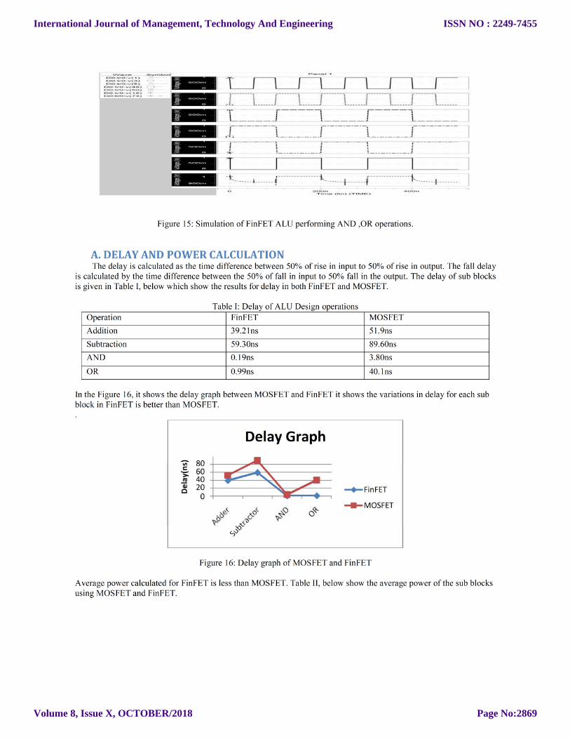
Figure 15: Simulation of FinFET ALU performing AND ,OR operations.
A. DELAY AND POWER CALCULATION The delay is calculated as the time difference between 50% of rise in input to 50% of rise in output. The fall delay
is calculated by the time difference between the 50% of fall in input to 50% fall in the output. The delay of sub blocks is given in Table I, below which show the results for delay in both FinFET and MOSFET.
Table I: Delay of ALU Design operations
Operation FinFET MOSFET
Addition 39.21ns 51.9ns
Subtraction 59.30ns 89.60ns
AND 0.19ns 3.80ns
OR 0.99ns 40.1ns
In the Figure 16, it shows the delay graph between MOSFET and FinFET it shows the variations in delay for each sub block in FinFET is better than MOSFET. .
Figure 16: Delay graph of MOSFET and FinFET
Average power calculated for FinFET is less than MOSFET. Table II, below show the average power of the sub blocks using MOSFET and FinFET.
International Journal of Management, Technology And Engineering
Volume 8, Issue X, OCTOBER/2018
ISSN NO : 2249-7455
Page No:2869

1.00E+00
1.00E-02
1.00E-04
1.00E-06
1.00E-08
1.00E-10
1.00E-12
Average Power Graph
FinFET
MOSFET
Adder Subtractor AND OR
Table II: Power of ALU Design operations
Operations FinFET MOSFET
Addition 0.041nw 24.45uw
Subtraction 0.097nw 19.5uw
AND 0.098pw 3.65uw
OR 0.10pw 1.25uw
In the Figure 17, it shows that the average power variations between MOSFET and FinFET for each sub-block of ALU and also shows that average power in FinFET is less than MOSFET.
Figure 17: Average Power analysis of MOSFET and FinFET
From both the architectures the average power and delay has been calculated below in table III, From this Table it is observed that delay and average power consumed by FinFET is far less than the delay and power consumed by MOSFET which results that the FinFET have faster speed less power dissipation than the MOSFET.
Table III: Comparison between Power and delay of FinFET and MOSFET
Delay Power
finFET 4.49ns 24uw
MOSFET 67.2ns 0.318mw
In the Figure 18, it Shows the power and delay variations in FinFET and MOSFET. In delay calculation it shows the delay obtained in MOSFET is far more than the delay obtained in FinFET. Also in power calculation it shows the average power consumption by FinFET is less than MOSFET.
International Journal of Management, Technology And Engineering
Volume 8, Issue X, OCTOBER/2018
ISSN NO : 2249-7455
Page No:2870
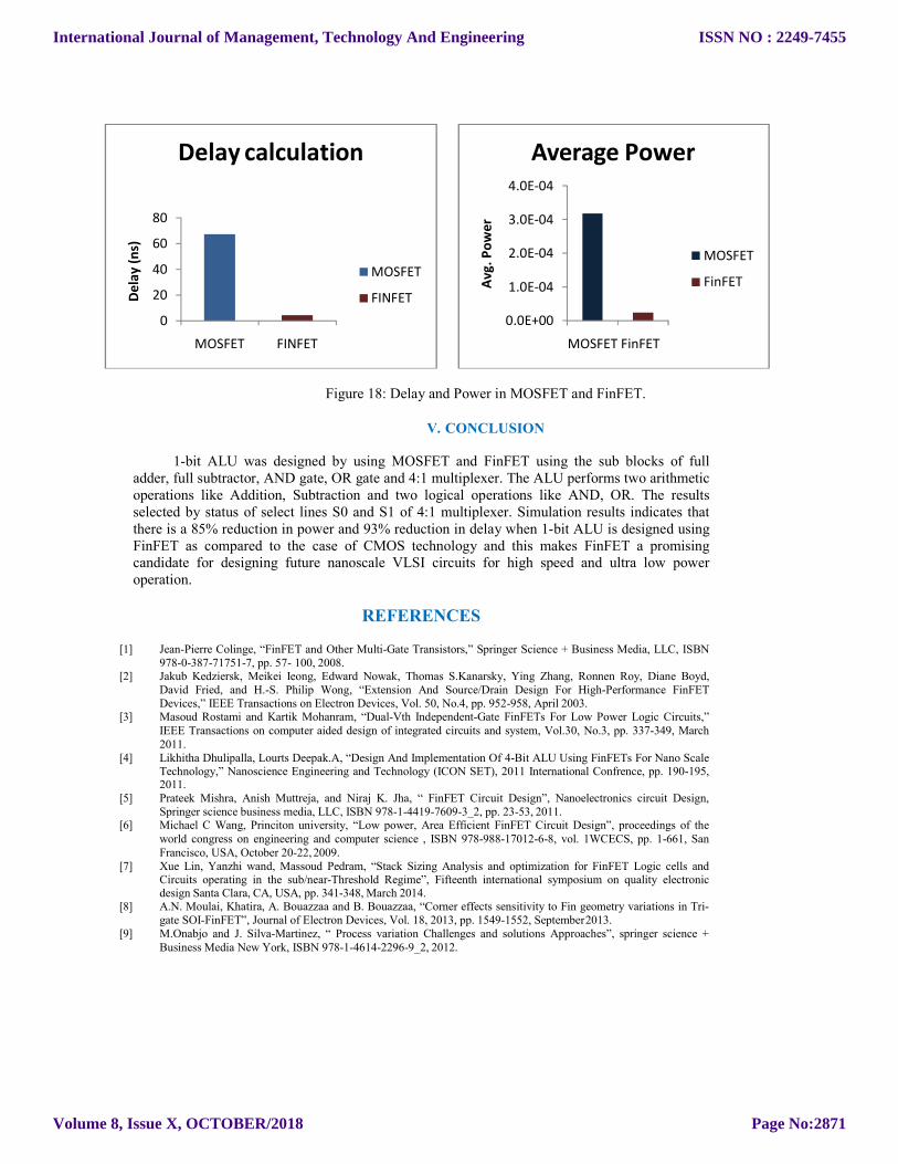
Figure 18: Delay and Power in MOSFET and FinFET.
V. CONCLUSION
1-bit ALU was designed by using MOSFET and FinFET using the sub blocks of full adder, full subtractor, AND gate, OR gate and 4:1 multiplexer. The ALU performs two arithmetic operations like Addition, Subtraction and two logical operations like AND, OR. The results selected by status of select lines S0 and S1 of 4:1 multiplexer. Simulation results indicates that there is a 85% reduction in power and 93% reduction in delay when 1-bit ALU is designed using FinFET as compared to the case of CMOS technology and this makes FinFET a promising candidate for designing future nanoscale VLSI circuits for high speed and ultra low power operation.
REFERENCES
[1] Jean-Pierre Colinge, “FinFET and Other Multi-Gate Transistors,” Springer Science + Business Media, LLC, ISBN 978-0-387-71751-7, pp. 57- 100, 2008.
[2] Jakub Kedziersk, Meikei Ieong, Edward Nowak, Thomas S.Kanarsky, Ying Zhang, Ronnen Roy, Diane Boyd, David Fried, and H.-S. Philip Wong, “Extension And Source/Drain Design For High-Performance FinFET Devices,” IEEE Transactions on Electron Devices, Vol. 50, No.4, pp. 952-958, April 2003.
[3] Masoud Rostami and Kartik Mohanram, “Dual-Vth Independent-Gate FinFETs For Low Power Logic Circuits,” IEEE Transactions on computer aided design of integrated circuits and system, Vol.30, No.3, pp. 337-349, March 2011.
[4] Likhitha Dhulipalla, Lourts Deepak.A, “Design And Implementation Of 4-Bit ALU Using FinFETs For Nano Scale Technology,” Nanoscience Engineering and Technology (ICON SET), 2011 International Confrence, pp. 190-195, 2011.
[5] Prateek Mishra, Anish Muttreja, and Niraj K. Jha, “ FinFET Circuit Design”, Nanoelectronics circuit Design, Springer science business media, LLC, ISBN 978-1-4419-7609-3_2, pp. 23-53, 2011.
[6] Michael C Wang, Princiton university, “Low power, Area Efficient FinFET Circuit Design”, proceedings of the world congress on engineering and computer science , ISBN 978-988-17012-6-8, vol. 1WCECS, pp. 1-661, San Francisco, USA, October 20-22, 2009.
[7] Xue Lin, Yanzhi wand, Massoud Pedram, “Stack Sizing Analysis and optimization for FinFET Logic cells and Circuits operating in the sub/near-Threshold Regime”, Fifteenth international symposium on quality electronic design Santa Clara, CA, USA, pp. 341-348, March 2014.
[8] A.N. Moulai, Khatira, A. Bouazzaa and B. Bouazzaa, “Corner effects sensitivity to Fin geometry variations in Tri-gate SOI-FinFET”, Journal of Electron Devices, Vol. 18, 2013, pp. 1549-1552, September 2013.
[9] M.Onabjo and J. Silva-Martinez, “ Process variation Challenges and solutions Approaches”, springer science + Business Media New York, ISBN 978-1-4614-2296-9_2, 2012.
Delay calculation
80
60
40
20
0
MOSFET
FINFET
MOSFET FINFET
Average Power 4.0E-04
3.0E-04
2.0E-04
1.0E-04
0.0E+00
MOSFET
FinFET
MOSFET FinFET
De
lay
(ns)
Avg
. Po
wer
International Journal of Management, Technology And Engineering
Volume 8, Issue X, OCTOBER/2018
ISSN NO : 2249-7455
Page No:2871