Handbook OPTIFLEX 1300 C - Max-Planck-Institut für Kernphysik
IEKP–KA/2005–6
ELEKTRONIK FUR DAS
WELTRAUM-EXPERIMENT AMS02UND
BILDGEBUNG IN DER STRAHLENMEDIZIN
Levin Jungermann
Zur Erlangung des akademischen Grades einesDOKTORS DER NATURWISSENSCHAFTEN
von der Fakultat fur Physikder Universitat Karlsruhe (TH)
genehmigte
DISSERTATION
von
Dipl. phys. Levin Jungermannaus Karlsruhe
Tag der mundlichen Prufung: 10.06.2005
Referent: Prof. Dr. Wim de Boer, Institut fur Experimentelle Kernphysik
Koreferent: Prof. Dr. Thomas Muller, Institut fur Experimentelle Kernphysik

Deutsche ZusammenfassungIn dieser Promotion werden zwei Anwendungen modernster Technologien fur den Nachweis von Teilchen
naher betrachtet. Im ersten Teil dieser Arbeit liegt der Schwerpunkt auf der Elektronikentwicklung fur das welt-raumgestutzte Hochenergiephysik-Experiment Alpha Magnetische Spektrometer (AMS02). Der zweite Teildieser Arbeit beschaftigt sich mit CMOS-Pixeldetektoren fur medizinische Anwendungen. Die Untersuchun-gen dazu wurden im Rahmen des EU-Projektes
”Silicon Ultra fast Cameras for electron and gamma sources In
Medical Applications“ (SUCIMA) durchgefuhrt.Seit 1910, als Wulf die ersten Messungen zur Abhangigkeit der Strahlungsintensitat von der Hohe gemacht
hat, spielt die Untersuchung der kosmischen Strahlung eine wichtige Rolle in der Teilchenphysik. So wurdenin der Hohenstrahlung das erste Mal Myonen (1937, Anderson und Neddermeyer) und Pionen (1947, Lattes etal.) gemessen, aber auch einige Hyperionen wurden in der kosmischen Strahlung entdeckt, z.B. das Ξ (1952,Armenteros et al.). In den letzten Jahrzehnten dominierten die großen Teilchenbeschleuniger (LEP, Tevatron,...)das Feld der Hochenergiephysik. Erst in den letzten Jahren hat die kosmische Strahlung wieder an Bedeutunggewonnen, da einerseits Phanomene entdeckt wurden, die in Beschleunigern auf der Erde nicht nachgestelltwerden konnen, aber auch neue Technologien zur Verfugung stehen, die es erlauben, Teilchendetektoren zubauen, die im Weltraum betrieben werden konnen.
Das AMS02-Projekt ist einer dieser neuen Teilchendetektoren zur Messung der primaren kosmischen Strah-lung außerhalb der Erdatmosphare. Mit einem Prototypensystem (AMS01) konnte 1998 das Potential diesesAufbaus wahrend einer zehntagigen Mission im Space Shuttle (STS-91) erfolgreich demonstriert werden. DerAMS02-Detektor wird ab 2008 fur mindestens drei Jahre auf der Internationalen Raumstation (ISS) das Spek-trum der primaren kosmischen Strahlung in einem Energiebereich von 300MeV bis 3TeV messen und hierbeieine vielfache Datenmenge aller bisherigen Experimente mit unerreichter Prazision aufzeichnen.
Der Standort von AMS02 auf der ISS und der Transport dort hin mit einem Space Shuttle stellen immenseAnforderungen an den Detektor und die Ausleseelektronik. Sie mussen den Vibrationen wahrend des Startswiderstehen konnen. Aber auch das Vakuum, die Temperaturschwankungen und die elektromagnetische Ver-traglichkeit stellen große Herausforderungen dar. Da keine Wartung des Detektors wahrend der Betriebszeitmoglich ist, mussen alle kritischen Systeme abgesichert und mehrfach vorhanden sein.
Das Institut fur Experimentelle Kernphysik (IEKP) der Universitat Karlsruhe (TH) ist seit 2002 verant-wortlich fur die Elektronik des Ubergangsstrahlungsdetektors (TRD), der von der RWTH Aachen gebaut wird.Die Entwicklung der Elektronik ist in mehrere Phasen unterteilt: Prototypenstadium, Entwicklungsphase (EM),Qualifikationsphasen 1 & 2 (QM1 & QM2) sowie die Produktion der Flugelektronik. Seit der Entwicklungs-phase ist das IEKP federfuhrend an der Entwicklung der Elektronik beteiligt.
Im Rahmen dieser Promotion wurde die Firmware der Datenreduktionskarte (UDR, detektorspezifischerTeil), der Niederspannungskarte (UPSFE) und der Kontrollkarte (S9011AU) fur die Stromversorgung erstellt.Dabei galt es besonders, die Anforderungen an die Verwaltung der Redundanz zu erfullen, um einen sicherenBetrieb der Ausleseelektronik zu gewahrleisten. Die Funktion der Elektronik wurde jeweils in den Phasen EMund QM1 mit einer Strahlzeit am CERN mit einem Prototypen des TRD erfolgreich uberpruft.
Ein weiteres Projekt in dieser Promotion war Entwicklung und Bau einer Testumgebung fur die Nieder-spannungskarte UPSFE. Mit Hilfe dieser Testumgebung kann die komplette Funktionalitat(1) der UPSFE ge-testet werden. Nach der Erprobungsphase in Karlsruhe wurde die Testumgebung erfolgreich zur Qualifikationder Vorproduktion der Elektronik am Chung-Shan Institute of Science and Technology in Taiwan zum Einsatzgebracht und wird auch wahrend der Produktion der Flugmodule genutzt werden.
Die Integrations- und Funktionstests auf Crate-Level sind am Institut fur Experimentelle Kernphysik er-folgreich abgeschlossen worden. In naher Zukunft werden die Tests zur Validierung der Weltraumtauglichkeit(Thermo-Vakuum-Test, Vibrationstest und Elektromagnetischer Interferenztest) auf Crate-Level beginnen, hiersind jedoch keine Probleme zu erwarten.
Strahlung spielt in der Medizin eine wichtige Rolle, sowohl in der Diagnostik als auch in der Therapie. DasZeitalter der Radiologie und -therapie begann 1895, als Wilhelm Conrad Rontgen die erste Aufnahme der Handseiner Frau mit den so genannten
”X-Strahlen“(2) machte. Es zeigte sich jedoch schnell, das eine sorgfaltige
Dosimetrie benotigt wird, um eine sichere Anwendung der Strahlung zu gewahrleisten.
(1)Die Aufgaben der UPSFE umfassen die Regulierung und Absicherung der ±2V fur die Eingangsverstarker (14Kanale), sowie das Setzen und Uberwachen von externen Kontroll- und Monitorleitungen (10 Kanale).
(2)Der Name X-Strahlung stammt aus der Zeit als auch die Begriffe α-,β- und γ- Strahlung gepragt wurden und istheute noch im Englischen als
”X-ray“gebrauchlich. Im Deutschen Sprachgebrauch hat sich jedoch der Begriff
Rontgen-Strahlen durchgesetzt.
1
Das SUCIMA-Projekt verfolgte den Ansatz, mit Wissen und Technologien aus der Hochenergiephysik dieDosimetrie in zwei Anwendungsbereichen der Strahlenmedizin, Brachytherapie (Dosimeter) und Hadronenthe-rapie (Strahlmonitor), zu verbessern. Zwei technologische Ansatze wurden dabei verfolgt, zum einen CMOS(3)-Sensoren, zum anderen SOI(4)-Sensoren. Neben der Entwicklung der Sensoren wurde auch ein Datenerfas-sungssystem (DAQ) mit USB2.0-Anbindung entworfen und verwirklicht. In der Konfiguration fur den Strahl-monitor kann das DAQ-System die kritischen Strahlparameter mit 10kHz uberwachen und notfalls einen Ab-bruch der Behandlung auslosen.
Neben den Anforderungen an das raumliche Auflosungsvermogen, die Auslesegeschwindigkeit und dieGroße der Detektoren spielt in diesen Anwendungen naturlich die Strahlenharte eine besondere Rolle. Im Rah-men dieser Arbeit wurden daher Studien an SUCCESSOR-I-Detektoren durchgefuhrt, mit der Zielsetzung, dieoptimale Pixelgeometrie fur einen Dosimetriedetektor zu bestimmen.
Der SUCCESSOR-I-Detektor wurde als Technologietrager entwickelt und besteht aus acht Pixelmatrizen,die jeweils 32 mal 32 Pixel umfassen und von denen jede eine andere Pixelgeometrie hat. Hierbei wurdenbei allen Pixeltypen die Erfahrungen mit den alteren Prototypen berucksichtigt. Zum Beispiel sind Source undDrain der Resettransistoren im Vergleich zum alten Layout vertauscht, um parasitare Ladungstransferpfade zuvermeiden.
Fur diese Studien wurden SUCCESSOR-I Detektoren mit einer Rontgen-Anlage in mehreren Dosisstufenbis 2Mrad bestrahlt und jeweils die wichtigsten Parameter der Pixel als Funktion der Dosis bestimmt. AlsEntscheidungskriterien kamen hierbei der Leckstrom, die Verstarkung im Pixel sowie die Ladungssammlungs-effizienz und das Signal-zu-Rauschen-Verhaltnis zum Tragen. An Hand der Pixelgeometrien 3 und 4 werdenbeispielhaft die Messergebnisse erklart und bewertet. Dabei dient Pixel 3 auf Grund seines Standarddesigns alsReferenz, und Pixel 4 ist als der fur das finale Design ausgewahlte Pixel vertreten.
In den Messungen konnte beobachtet werden, dass alle acht Pixelgeometrien im getesteten Dosisbereichunbedenklich sind in Hinsicht auf eine mogliche Degradation der Ladungssammlungseffizienz, der Verstarkungund des Signal zu Rauschen Verhaltnisses. Als wichtigstes Entscheidungskriterium hat sich das Leckstromver-halten erwiesen. Pixel 4 zeigte mit den geringsten Anstieg des Leckstromes mit wachsender Dosis.
Neben den eigentlichen Messwerten werden auch Phanomene diskutiert, die wahrend der Messungen auf-traten und diese beeinflusst haben. Zum einen ist der Digitalteil des Detektors nicht strahlenhart und muss daherabgeschirmt werden, zum anderen haben sich die analogen Ausgangstreiber durch die großeren Leckstrome sostark erhitzt, dass sich die Pedestals stark verschoben haben.
Zusammenfassend kann man sagen, dass Pixellayout 4 von den acht untersuchten Layouts am besten fureine Anwendung in der Brachytherapie geeignet ist: Die Ladungssammlungseffizienz bleibt von der Bestrah-lung unbeeinflußt, ebenso wie die Verstarkung des Pixels und das Signal-zu-Rauschen Verhaltnis. Dank seinermittleren Verstarkung liegt die Sensitivitat von Pixel 4 ebenfalls im optimalen Bereich fur diese Anwendung.Ein weiteres wichtiges Merkmal von Layout 4 ist der niedrige Leckstrom, insbesondere da auch der Anstiegmit der Dosis der geringste aller untersuchten Layouts war.
Die SUCIMA Kollaboration hat einen Detektor, SUCCESSOR-V, basierend auf diesem Layout entwi-ckelt und produziert. Im klinischen Einsatz wird dieser Detektor es erlauben mehr als 10.000 Messungen unterungunstigsten Bedingungen (Messdauer: 10s, Dosisleistung: 20rad/s) durchzufuhren, bevor er ersetzt werdenmuss. Altere Designs hatten bereits nach einigen hundert Messungen keine zuverlassigen Daten mehr geliefert.
Das Verhalten von Detektoren in starken Magnetfeldern spielt heute sowohl in der Medizin als auch in derHochenergiephysik eine wichtige Rolle. In einer Studie wurden daher die Signalhohe und -breite als Funktionder Feldstarke bis 6T bestimmt. Dabei wurden zwei Konfigurationen vermessen: Magnetfeld parallel (a) bzw.senkrecht (b) zur Sensoroberflache. Bei diesen Messungen wurde festgestellt, dass die Signalstarke in Konfigu-ration (a) mit zunehmender Feldstarke abnimmt, wahrend sie in Konfiguration (b) zunimmt. Dies kann mit Hilfeeines einfachen Modells basierend auf der Lorentzkraft verstanden werden. In Fall (a) wird die Geschwindig-keitskomponente in Richtung des Kontaktes durch die Lorentzkraft verringert, wahrend sie im Fall (b) verstarktwird.
(3)CMOS: Complementary Metal Oxide Semiconductor(4)SOI: Silicon On Insulator
2
Space-Qualified Electronicsfor the AMS02 Experiment
andMedical Radiation Imaging
Levin Jungermann
23rd May 2005


Contents
Introduction 1
1 The AMS02 Experiment 31.1 Precursor Experiments . . . . . . . . . . . . . . . . . . . . . . . . . . . . . . . . . 4
1.1.1 Balloon Experiments . . . . . . . . . . . . . . . . . . . . . . . . . . . . . . 41.1.2 Space Experiments . . . . . . . . . . . . . . . . . . . . . . . . . . . . . . . 41.1.3 The AMS01 Experiment . . . . . . . . . . . . . . . . . . . . . . . . . . . . 5
1.2 The AMS02 Detector . . . . . . . . . . . . . . . . . . . . . . . . . . . . . . . . . . 71.2.1 Transition Radiation Detector (TRD) . . . . . . . . . . . . . . . . . . . . . 7
TRD Gas System . . . . . . . . . . . . . . . . . . . . . . . . . . . . . . . . 9Performance of the TRD . . . . . . . . . . . . . . . . . . . . . . . . . . . . 10
1.2.2 Time of Flight (TOF) . . . . . . . . . . . . . . . . . . . . . . . . . . . . . . 10Performance of the TOF . . . . . . . . . . . . . . . . . . . . . . . . . . . . 11
1.2.3 Silicon Tracker . . . . . . . . . . . . . . . . . . . . . . . . . . . . . . . . . 12Tracker Thermal Control System . . . . . . . . . . . . . . . . . . . . . . . . 13The Superconducting Magnet . . . . . . . . . . . . . . . . . . . . . . . . . 14Performance of the Silicon Tracker . . . . . . . . . . . . . . . . . . . . . . 15
1.2.4 Anti-Coincidence Counter (ACC) . . . . . . . . . . . . . . . . . . . . . . . 16Performance of the ACC . . . . . . . . . . . . . . . . . . . . . . . . . . . . 17
1.2.5 Ring Image Cherenkov Counter (RICH) . . . . . . . . . . . . . . . . . . . . 17Performance of the RICH . . . . . . . . . . . . . . . . . . . . . . . . . . . 18
1.2.6 Electromagnetic Calorimeter (ECAL) . . . . . . . . . . . . . . . . . . . . . 19Performance of the ECAL . . . . . . . . . . . . . . . . . . . . . . . . . . . 19
1.2.7 Star Tracker & GPS . . . . . . . . . . . . . . . . . . . . . . . . . . . . . . 20Performance of the Star Tracker & the GPS . . . . . . . . . . . . . . . . . . 21
1.2.8 Detector Environment . . . . . . . . . . . . . . . . . . . . . . . . . . . . . 211.3 Physics with the AMS02 Detector . . . . . . . . . . . . . . . . . . . . . . . . . . . 22
1.3.1 Cosmic Rays . . . . . . . . . . . . . . . . . . . . . . . . . . . . . . . . . . 231.3.2 Cosmic Rays - Charged Particles . . . . . . . . . . . . . . . . . . . . . . . . 23
Element Abundances . . . . . . . . . . . . . . . . . . . . . . . . . . . . . . 23Cosmic Ray Energy Spectra . . . . . . . . . . . . . . . . . . . . . . . . . . 24Acceleration Mechanisms . . . . . . . . . . . . . . . . . . . . . . . . . . . 26
1.3.3 Cosmic Rays - Anti-Matter . . . . . . . . . . . . . . . . . . . . . . . . . . . 291.3.4 Cosmic Rays - High Energy Gammas . . . . . . . . . . . . . . . . . . . . . 32
Acceleration Mechanisms . . . . . . . . . . . . . . . . . . . . . . . . . . . 331.3.5 Dark Matter Search . . . . . . . . . . . . . . . . . . . . . . . . . . . . . . . 341.3.6 Transition Radiation . . . . . . . . . . . . . . . . . . . . . . . . . . . . . . 37
i
2 Space-Grade Electronics for the AMS02 Detector 392.1 Overall system design . . . . . . . . . . . . . . . . . . . . . . . . . . . . . . . . . . 402.2 AMS02 Electronics . . . . . . . . . . . . . . . . . . . . . . . . . . . . . . . . . . . 40
2.2.1 DAQ systems . . . . . . . . . . . . . . . . . . . . . . . . . . . . . . . . . . 412.2.2 Slow-Control & Monitoring . . . . . . . . . . . . . . . . . . . . . . . . . . 422.2.3 Trigger . . . . . . . . . . . . . . . . . . . . . . . . . . . . . . . . . . . . . 43
2.3 Electronics for the TRD . . . . . . . . . . . . . . . . . . . . . . . . . . . . . . . . . 452.3.1 The TRD electronics crate - U-Crate . . . . . . . . . . . . . . . . . . . . . . 472.3.2 U-Backplane - UBP & UBPv2 . . . . . . . . . . . . . . . . . . . . . . . . . 472.3.3 J-Interface - JINF . . . . . . . . . . . . . . . . . . . . . . . . . . . . . . . . 482.3.4 U-Data-Reduction - UDR2 . . . . . . . . . . . . . . . . . . . . . . . . . . . 502.3.5 U-Front-End - UFE . . . . . . . . . . . . . . . . . . . . . . . . . . . . . . . 512.3.6 Universal Slow Control Module - USCM . . . . . . . . . . . . . . . . . . . 522.3.7 U-High-Voltage-Generator - UHVG . . . . . . . . . . . . . . . . . . . . . . 532.3.8 U-Power-Supply-for-Front-End - UPSFE . . . . . . . . . . . . . . . . . . . 55
UPSFEv2 . . . . . . . . . . . . . . . . . . . . . . . . . . . . . . . . . . . . 552.3.9 The U Power Distribution Box - UPD . . . . . . . . . . . . . . . . . . . . . 572.3.10 UPD Electronics - S9011AU . . . . . . . . . . . . . . . . . . . . . . . . . . 582.3.11 UPD Filter 28V - S9011B . . . . . . . . . . . . . . . . . . . . . . . . . . . 592.3.12 DC/DC-Converter . . . . . . . . . . . . . . . . . . . . . . . . . . . . . . . 592.3.13 Communication Protocols . . . . . . . . . . . . . . . . . . . . . . . . . . . 61
AMSwire . . . . . . . . . . . . . . . . . . . . . . . . . . . . . . . . . . . . 61CAN-Bus . . . . . . . . . . . . . . . . . . . . . . . . . . . . . . . . . . . . 61LeCroy bus . . . . . . . . . . . . . . . . . . . . . . . . . . . . . . . . . . . 61Dallas 1-wire Bus . . . . . . . . . . . . . . . . . . . . . . . . . . . . . . . . 62
2.4 Firmware Programming . . . . . . . . . . . . . . . . . . . . . . . . . . . . . . . . . 632.4.1 FPGA and Fuse/Anti-Fuse basics . . . . . . . . . . . . . . . . . . . . . . . 632.4.2 Introduction into VHDL & Design Flow . . . . . . . . . . . . . . . . . . . 64
Introduction into VHDL . . . . . . . . . . . . . . . . . . . . . . . . . . . . 65Design flow . . . . . . . . . . . . . . . . . . . . . . . . . . . . . . . . . . . 66
2.4.3 UDR Sequencer . . . . . . . . . . . . . . . . . . . . . . . . . . . . . . . . 67First measurement results . . . . . . . . . . . . . . . . . . . . . . . . . . . 70
2.4.4 The UPSFEv2 Firmware Programme . . . . . . . . . . . . . . . . . . . . . 722.4.5 The S9011AU Firmware Programme . . . . . . . . . . . . . . . . . . . . . 74
2.5 Production and Qualification . . . . . . . . . . . . . . . . . . . . . . . . . . . . . . 752.5.1 Design Process & Production Procedures . . . . . . . . . . . . . . . . . . . 75
Prototyping . . . . . . . . . . . . . . . . . . . . . . . . . . . . . . . . . . . 75Engineering Modules - EM . . . . . . . . . . . . . . . . . . . . . . . . . . . 75Qualification Modules - QM . . . . . . . . . . . . . . . . . . . . . . . . . . 75Flight Modules - FM . . . . . . . . . . . . . . . . . . . . . . . . . . . . . . 76Production Procedures . . . . . . . . . . . . . . . . . . . . . . . . . . . . . 76
2.5.2 Space Qualification Procedure . . . . . . . . . . . . . . . . . . . . . . . . . 77Single Board Level Tests . . . . . . . . . . . . . . . . . . . . . . . . . . . . 77Crate Level Tests . . . . . . . . . . . . . . . . . . . . . . . . . . . . . . . . 78
2.5.3 Electro-Magnetic Interference Test - EMI Test . . . . . . . . . . . . . . . . 782.5.4 Environmental Stress Screening Test - ESS . . . . . . . . . . . . . . . . . . 792.5.5 Vibration Test . . . . . . . . . . . . . . . . . . . . . . . . . . . . . . . . . . 802.5.6 Thermo-Vacuum Test - TVT . . . . . . . . . . . . . . . . . . . . . . . . . . 802.5.7 EM test backplane . . . . . . . . . . . . . . . . . . . . . . . . . . . . . . . 812.5.8 QM1 test backplane . . . . . . . . . . . . . . . . . . . . . . . . . . . . . . 812.5.9 UPSFEv2 test backplane . . . . . . . . . . . . . . . . . . . . . . . . . . . . 82
ii
2.5.10 Beam Tests . . . . . . . . . . . . . . . . . . . . . . . . . . . . . . . . . . . 85
EM beam test - October 2002 . . . . . . . . . . . . . . . . . . . . . . . . . 85
QM1 beam test - October 2003 . . . . . . . . . . . . . . . . . . . . . . . . . 86
3 Silicon Sensors 893.1 Interaction Of Radiation With Matter . . . . . . . . . . . . . . . . . . . . . . . . . . 89
3.1.1 Charged Particles . . . . . . . . . . . . . . . . . . . . . . . . . . . . . . . . 89
3.1.2 Photons . . . . . . . . . . . . . . . . . . . . . . . . . . . . . . . . . . . . . 92
3.1.3 Charge Carrier Generation in Semiconductor Materials . . . . . . . . . . . . 93
3.2 Position Sensitive Detectors . . . . . . . . . . . . . . . . . . . . . . . . . . . . . . 94
3.2.1 Microstrip Detectors . . . . . . . . . . . . . . . . . . . . . . . . . . . . . . 94
3.2.2 Pixel Devices . . . . . . . . . . . . . . . . . . . . . . . . . . . . . . . . . . 95
Pad Detectors . . . . . . . . . . . . . . . . . . . . . . . . . . . . . . . . . . 96
Hybrid Pixel Detector . . . . . . . . . . . . . . . . . . . . . . . . . . . . . 96
Charge Coupled Device - CCD . . . . . . . . . . . . . . . . . . . . . . . . . 97
Monolithic Pixel Detectors . . . . . . . . . . . . . . . . . . . . . . . . . . . 97
DEPFET . . . . . . . . . . . . . . . . . . . . . . . . . . . . . . . . . 98
CMOS . . . . . . . . . . . . . . . . . . . . . . . . . . . . . . . . . . 99
SOI . . . . . . . . . . . . . . . . . . . . . . . . . . . . . . . . . . . . 101
3.3 A Comparison of Detector Technologies . . . . . . . . . . . . . . . . . . . . . . . . 102
3.4 Radiation Damage . . . . . . . . . . . . . . . . . . . . . . . . . . . . . . . . . . . 104
3.4.1 Bulk Damage . . . . . . . . . . . . . . . . . . . . . . . . . . . . . . . . . . 104
3.4.2 Surface Damage . . . . . . . . . . . . . . . . . . . . . . . . . . . . . . . . 106
4 Medical Radiation Imaging 1094.1 SUCIMA . . . . . . . . . . . . . . . . . . . . . . . . . . . . . . . . . . . . . . . . 109
4.1.1 Intravascular Brachytherapy . . . . . . . . . . . . . . . . . . . . . . . . . . 109
4.1.2 Hadron Therapy . . . . . . . . . . . . . . . . . . . . . . . . . . . . . . . . 111
Beam Monitor . . . . . . . . . . . . . . . . . . . . . . . . . . . . . . . . . 112
SLIM . . . . . . . . . . . . . . . . . . . . . . . . . . . . . . . . . . . . . . 113
4.1.3 SUCIMA – Summary Detector Specifications . . . . . . . . . . . . . . . . . 115
4.2 SUCIMA Medical Detectors . . . . . . . . . . . . . . . . . . . . . . . . . . . . . . 116
4.2.1 Silicon Micro-Strip Detectors . . . . . . . . . . . . . . . . . . . . . . . . . 116
4.2.2 CMOS pixel detectors . . . . . . . . . . . . . . . . . . . . . . . . . . . . . 117
MIMOSA-V . . . . . . . . . . . . . . . . . . . . . . . . . . . . . . . . . . 117
MIMOSA-V back-thinned . . . . . . . . . . . . . . . . . . . . . . . . . . . 118
SUCCESSOR-I . . . . . . . . . . . . . . . . . . . . . . . . . . . . . . . . . 120
SUCCESSOR-II . . . . . . . . . . . . . . . . . . . . . . . . . . . . . . . . 123
SUCCESSOR-IV / MimoTERA . . . . . . . . . . . . . . . . . . . . . . . . 124
4.2.3 SOI pixel detectors . . . . . . . . . . . . . . . . . . . . . . . . . . . . . . . 125
4.3 Data Acquisition System . . . . . . . . . . . . . . . . . . . . . . . . . . . . . . . . 126
4.3.1 USB2.0 Data Acquisition System . . . . . . . . . . . . . . . . . . . . . . . 126
4.3.2 Repeater . . . . . . . . . . . . . . . . . . . . . . . . . . . . . . . . . . . . 128
4.3.3 Detector Hybrid . . . . . . . . . . . . . . . . . . . . . . . . . . . . . . . . 129
4.4 LabView Software for USB-DAQ . . . . . . . . . . . . . . . . . . . . . . . . . . . 129
4.4.1 Internal Structure . . . . . . . . . . . . . . . . . . . . . . . . . . . . . . . . 130
iii

5 Measurements with the SUCCESSOR-I CMOS pixel sensor 1335.1 Setup & Software . . . . . . . . . . . . . . . . . . . . . . . . . . . . . . . . . . . . 133
5.1.1 X-Ray Irradiation Setup in Karlsruhe . . . . . . . . . . . . . . . . . . . . . 1335.1.2 Measurement Setup at LEPSI . . . . . . . . . . . . . . . . . . . . . . . . . 1345.1.3 Measurement & Irradiation Procedure . . . . . . . . . . . . . . . . . . . . . 135
5.2 Radiation Tolerance Studies - Side Remarks . . . . . . . . . . . . . . . . . . . . . . 1375.2.1 Non-Radiation Hard Digital Part . . . . . . . . . . . . . . . . . . . . . . . 1375.2.2 Inhomogeneous Pedestals . . . . . . . . . . . . . . . . . . . . . . . . . . . 137
5.3 Radiation Tolerance Studies - Results . . . . . . . . . . . . . . . . . . . . . . . . . 1395.3.1 SUCCESSOR-I – Pixel 3 . . . . . . . . . . . . . . . . . . . . . . . . . . . . 1415.3.2 SUCCESSOR-I – Pixel 4 . . . . . . . . . . . . . . . . . . . . . . . . . . . . 1455.3.3 Summary . . . . . . . . . . . . . . . . . . . . . . . . . . . . . . . . . . . . 149
Choosing a pixel geometry . . . . . . . . . . . . . . . . . . . . . . . . . . . 1525.4 CMOS Pixel Sensors in Magnetic Fields . . . . . . . . . . . . . . . . . . . . . . . . 153
Summary 157
A LeCroy Bus data word definition 159
B UPSFEv2 firmware manual 161B.1 Control Words & Feedback Registers . . . . . . . . . . . . . . . . . . . . . . . . . 162
B.1.1 Power-up Detection . . . . . . . . . . . . . . . . . . . . . . . . . . . . . . . 162B.1.2 2nd Actel . . . . . . . . . . . . . . . . . . . . . . . . . . . . . . . . . . . . 162B.1.3 Linear Regulators Half A . . . . . . . . . . . . . . . . . . . . . . . . . . . . 162B.1.4 Linear Regulators Half D . . . . . . . . . . . . . . . . . . . . . . . . . . . . 162B.1.5 UHVG . . . . . . . . . . . . . . . . . . . . . . . . . . . . . . . . . . . . . 162B.1.6 UDR2 . . . . . . . . . . . . . . . . . . . . . . . . . . . . . . . . . . . . . . 162B.1.7 JINF . . . . . . . . . . . . . . . . . . . . . . . . . . . . . . . . . . . . . . 163B.1.8 Linear Regulator trip counters . . . . . . . . . . . . . . . . . . . . . . . . . 163B.1.9 External monitor lines trip counters . . . . . . . . . . . . . . . . . . . . . . 163
B.2 Backplane Connections - LeCroy Bus . . . . . . . . . . . . . . . . . . . . . . . . . 163B.3 FPGA pin assignment . . . . . . . . . . . . . . . . . . . . . . . . . . . . . . . . . . 164B.4 UPSFEv2 Command & Read Registers Tables . . . . . . . . . . . . . . . . . . . . . 165
C S9011AU firmware manual 169C.1 Command & Feedback Registers . . . . . . . . . . . . . . . . . . . . . . . . . . . . 170
C.1.1 Power-up Detection . . . . . . . . . . . . . . . . . . . . . . . . . . . . . . . 170C.1.2 2nd Actel . . . . . . . . . . . . . . . . . . . . . . . . . . . . . . . . . . . . 170C.1.3 DC/DC converters half L . . . . . . . . . . . . . . . . . . . . . . . . . . . . 170C.1.4 DC/DC converters half H . . . . . . . . . . . . . . . . . . . . . . . . . . . . 170
C.2 Backplane Connections - LeCroy Bus . . . . . . . . . . . . . . . . . . . . . . . . . 170C.3 FPGA Pin Assignment . . . . . . . . . . . . . . . . . . . . . . . . . . . . . . . . . 171C.4 S9011AU Command & Read Registers Tables . . . . . . . . . . . . . . . . . . . . . 172
D Analysis Algorithms for SUCIMA 175D.1 LabView . . . . . . . . . . . . . . . . . . . . . . . . . . . . . . . . . . . . . . . . . 175
D.1.1 Pedestals . . . . . . . . . . . . . . . . . . . . . . . . . . . . . . . . . . . . 175D.1.2 Noise . . . . . . . . . . . . . . . . . . . . . . . . . . . . . . . . . . . . . . 175D.1.3 Common Mode Noise . . . . . . . . . . . . . . . . . . . . . . . . . . . . . 176D.1.4 Bad Pixel Masking . . . . . . . . . . . . . . . . . . . . . . . . . . . . . . . 176D.1.5 Cluster Search . . . . . . . . . . . . . . . . . . . . . . . . . . . . . . . . . 177
D.2 Mathematica . . . . . . . . . . . . . . . . . . . . . . . . . . . . . . . . . . . . . . 177
iv

E Measurement Results SUCCESSOR-I 183E.1 SUCCESSOR-I – Pixel 0 . . . . . . . . . . . . . . . . . . . . . . . . . . . . . . . . 183E.2 SUCCESSOR-I – Pixel 1 . . . . . . . . . . . . . . . . . . . . . . . . . . . . . . . . 184E.3 SUCCESSOR-I – Pixel 2 . . . . . . . . . . . . . . . . . . . . . . . . . . . . . . . . 184E.4 SUCCESSOR-I – Pixel 5 . . . . . . . . . . . . . . . . . . . . . . . . . . . . . . . . 186E.5 SUCCESSOR-I – Pixel 6 . . . . . . . . . . . . . . . . . . . . . . . . . . . . . . . . 187E.6 SUCCESSOR-I – Pixel 7 . . . . . . . . . . . . . . . . . . . . . . . . . . . . . . . . 188
Acknowledgements 189
List of Figures 191
List of Tables 195
Bibliography 197
Glossary 203
Alphabetical Index 209
v

Introduction
This thesis takes a closer look at two applications of modern technology in particle detection. In thefirst part of the thesis the focus is set on the read out and slow-control electronics of the spaceborneHigh Energy Physics experiment Alpha Magnetic Spectrometer (AMS02). In the second part theemphasis is set on CMOS sensors for particle detection in medical applications. The latter was donewithin the framework of the EU project “Silicon Ultra fast Cameras for electron and gamma sourcesIn Medical Applications” (SUCIMA).
Ever since their discovery at the beginning of the 20th century, cosmic rays have been fascinatingphysicists all over the world. Soon many experiments, both earthbound and airborne, were done toinvestigate the nature of the cosmic rays. It was evident almost from the beginning, that access to theprimary particles is only possible in the upper atmosphere or above it. Due to the interaction of theincoming particles with the atmosphere of the Earth, earthbound experiments are limited to particleswith low interaction probabilities, like neutrinos, or studies of secondary effects, like showers orCherenkov light.
AMS02 is the latest experiment in a 30-year tradition of spaceborne instruments to measure thecomposition and spectra of the primary cosmic rays in the energy range of 300MeV to 3TeV . Start-ing in 2008 the 3+ year long mission of AMS02 will yield an unprecedented amount of data withan unrivalled precision. This data will allow to refine the existing models for the acceleration andpropagation of cosmic rays. The high precision data, especially the positron fraction and the highenergy gamma spectrum, will also lead to a better understanding of the theories for Dark Matter. Ad-ditionally, the measurements will be essential for any long duration manned space mission outside ofEarth’s protective environment.
The location of AMS02 on the International Space Station (ISS) and the transport there by a SpaceShuttle impose very stringent requirements on the detector itself and its infrastructure. All componentsmust be able to withstand the enormous vibrations during the launch, but also the temperature cyclesand the vacuum. All critical parts of AMS02 have to be protected and redundant, as no maintenanceis possible during the lifetime of the experiment.
Within the framework of this thesis space-grade electronics for the Transition Radiation Detector(TRD) of AMS02 were developed. The Institut fur Experimentelle Kernphysik at the University ofKarlsruhe (TH) is responsible for the electronics of the TRD and has been actively involved in thedesign, qualification and production process since the engineering phase. Within the framework ofthis thesis the firmware codes for the data reduction card (UDR, detector specific part), the low voltageregulator card (UPSFE) and the controller card for the power supply (S9011AU) were developed. Afurther project was the design and construction of a testbed for the UPSFE. This testbed was usedduring the quality control of the pre-production of the electronics at the Chung-Shan Institute ofScience and Technology in Taiwan and will be also used during the production of the flight hardware.
In chapter 1 an introduction to the detector and its subsystems is given(1), followed by a shortreview of the physics involved in the acceleration of cosmic rays. A detailed description of the elec-tronics of AMS02 is presented in chapter 2. Here a special emphasis is put on the electronics of theTRD and the developments done within the framework of this thesis.
(1)Please note, that all specifications and information on AMS02 reflect the status of April 2005 and are subject topossible changes as the integration of the detector proceeds.
1
2 INTRODUCTION
Radiation has become more and more important in medicine, both in diagnostics and in treatment,ever since William Conrad Rontgen took the first X-ray image of his wife’s hand in 1895. This newtechnique induced an over-enthusiastic application of it in the years after its discovery. Through tragicevents, caused by the side effects of the radiation, it soon became obvious that a thorough dosimetryhad to go hand in hand with the use of radiation in medicine. From in-vivo dosimetry to digital X-raysystems, today’s state of the art detectors and electronics cover an enormous field of dosimetry andimaging applications.
The aim of the SUCIMA project was to develop systems for dosimetry of extended sources and on-line beam monitoring, benefiting from the existing know-how in the High Energy Physics communityand the possibilities of new technologies in the detector design and production. The two focus pointsof the SUCIMA project were inspired by brachytherapy, where a high activity radioactive source isused to suppress the growth of scar tissue after an angioplasty, and from hadron therapy, where anintense beam of ions is used to treat a tumour.
Two technological approaches were pursued for the detector design by the SUCIMA collabo-ration: CMOS(2) and SOI(3). The CMOS technology is a standard process widely used throughoutindustry in different variations, where the structure is processed on top of a low resistivity wafer. Theuse of this technology allows to produce devices at reasonable costs while benefiting from standarddesigns existing in industry, even though the detectors suffer from the low signal due to the thin sen-sitive volume (< 15µm). In the SOI technology the device is made up from two wafers separated bya layer of silicon oxide. The device wafer is thinned down to a few micrometres to optimise the per-formance of the electronics. The handle wafer, normally a low resistivity wafer unused by industrialapplications, can be replaced by a detector-grade wafer and used as fully depleted sensitive volume,overcoming the limitations of CMOS detectors, namely the low signal.
Especially in the application as a dosimeter for the brachytherapy, the detectors have to be able towithstand very high doses, as the sources have activities in the order of a few GBq. The second focuspoint of this thesis was to investigate the radiation hardness of eight pixel geometries on a prototypeCMOS detector of the SUCIMA collaboration using an X-ray system. Based on the obtained results,a recommendation regarding the pixel layout was made for the final device of the SUCIMA project.
Chapter 3 gives an overview of the interaction of radiation with matter and the different tech-nologies of position sensitive radiation detectors. In chapter 4 the SUCIMA project and its medicalapplications are introduced together with the detectors and the data acquisition system developedwithin this framework. The measurement setups used for the radiation hardness studies and the re-sults obtained are presented in chapter 5, followed by a summary of the measurements with CMOSdetectors in high magnetic fields.
(2)CMOS: Complementary Metal Oxide Semiconductor(3)SOI: Silicon On Insulator
Chapter 1
The AMS02 Experiment
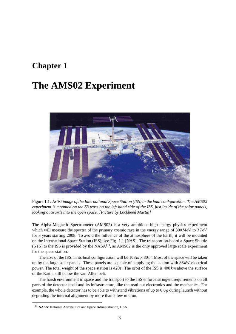
Figure 1.1: Artist image of the International Space Station (ISS) in the final configuration. The AMS02experiment is mounted on the S3 truss on the left hand side of the ISS, just inside of the solar panels,looking outwards into the open space. [Picture by Lockheed Martin]
The Alpha-Magnetic-Spectrometer (AMS02) is a very ambitious high energy physics experimentwhich will measure the spectra of the primary cosmic rays in the energy range of 300MeV to 3TeVfor 3 years starting 2008. To avoid the influence of the atmosphere of the Earth, it will be mountedon the International Space Station (ISS), see Fig. 1.1 [NAS]. The transport on-board a Space Shuttle(STS) to the ISS is provided by the NASA(1), as AMS02 is the only approved large scale experimentfor the space station.
The size of the ISS, in its final configuration, will be 108m×80m. Most of the space will be takenup by the large solar panels. These panels are capable of supplying the station with 86kW electricalpower. The total weight of the space station is 420 t. The orbit of the ISS is 400km above the surfaceof the Earth, still below the van-Allen belt.
The harsh environment in space and the transport to the ISS enforce stringent requirements on allparts of the detector itself and its infrastructure, like the read out electronics and the mechanics. Forexample, the whole detector has to be able to withstand vibrations of up to 6.8g during launch withoutdegrading the internal alignment by more than a few micron.
(1)NASA: National Aeronautics and Space Administration, USA
3

4 THE AMS02 EXPERIMENT
On the following pages a short introduction into precursor experiments is given. In the nextsection AMS02, with its various subdetectors, is described in detail. At the end of this chapter theenvironmental conditions for a space experiment like AMS02 will be illustrated.
1.1 Precursor Experiments
From the aurora borealis to the first recorded observations of supernovas, high energetic cosmic rayshave been a major motivation for scientists for quite a long time.
After some first measurements on the intensity of ionising radiation as a function of height by Wulfin 1910 on the Eifel Tower in Paris, Hess built the first balloon experiments in 1911/1912 [Hes12].These measurements earned him the Nobel Prize in 1936.
Since then balloon borne experiments have been the choice for measurements of cosmic rays, if theinfluence of the atmosphere was to be minimised. Only in recent years the possibility of spacebornehigh energy physics experiments has become available.
1.1.1 Balloon Experiments
Even though balloon experiments have been getting more and more sophisticated since the days ofHess, they still suffer from the same draw-backs as in those days.
Even with a maximum flight altitude of about 50km, there is still ∼ 3g of atmosphere(2) above thedetector, which strongly limits the access to primary cosmic rays.
Figure 1.2: The BESS balloon experiment be-fore launch. [Source: Goddard Space FlightCenter]
The maximum weight of a balloon experiment isstrongly limited as the high altitude balloons can onlycarry up to ∼ 3.5 t. This imposes very stringent re-quirements on the detector design, solvable in mostcases only by compromises limiting the physics pos-sibilities of the experiment, for example the openingangle.
A third problem is the short flight time of balloonborne experiments, as the statistics that can be col-lected during the flight are directly proportional to theflight time. The flight time for the recent experimentsvaries from 1 to 14 days.
The most important balloon experiments in re-cent decades were BESS(3) [Wan02], shown in Fig.1.2, and HEAT(4) [Bow99]. They were able to sup-ply very interesting information on the spectrum andmass composition of cosmic rays. The most recentballoon flight was the Antarctica mission of TRACER(5), which lasted 14 days [TRA].
1.1.2 Space Experiments
Since the early days of spaceflight, experiments on the composition and spectra of the cosmic rayswere made. For example, the moon missions, Apollo 16 and 17, carried cosmic ray detectors consist-ing of different absorber plates, which were analysed on Earth after the missions.
(2)g is the short form of g/cm2, the remanent pressure. It is a naming convention used by the various collaborationsoperating balloon experiments.
(3)BESS: Balloon-borne Experiment with a Superconducting Solenoidal magnet(4)HEAT: High-Energy Antimatter Telescope(5)TRACER: Transition Radiation Array for Cosmic Energetic Rays
1.1 PRECURSOR EXPERIMENTS 5
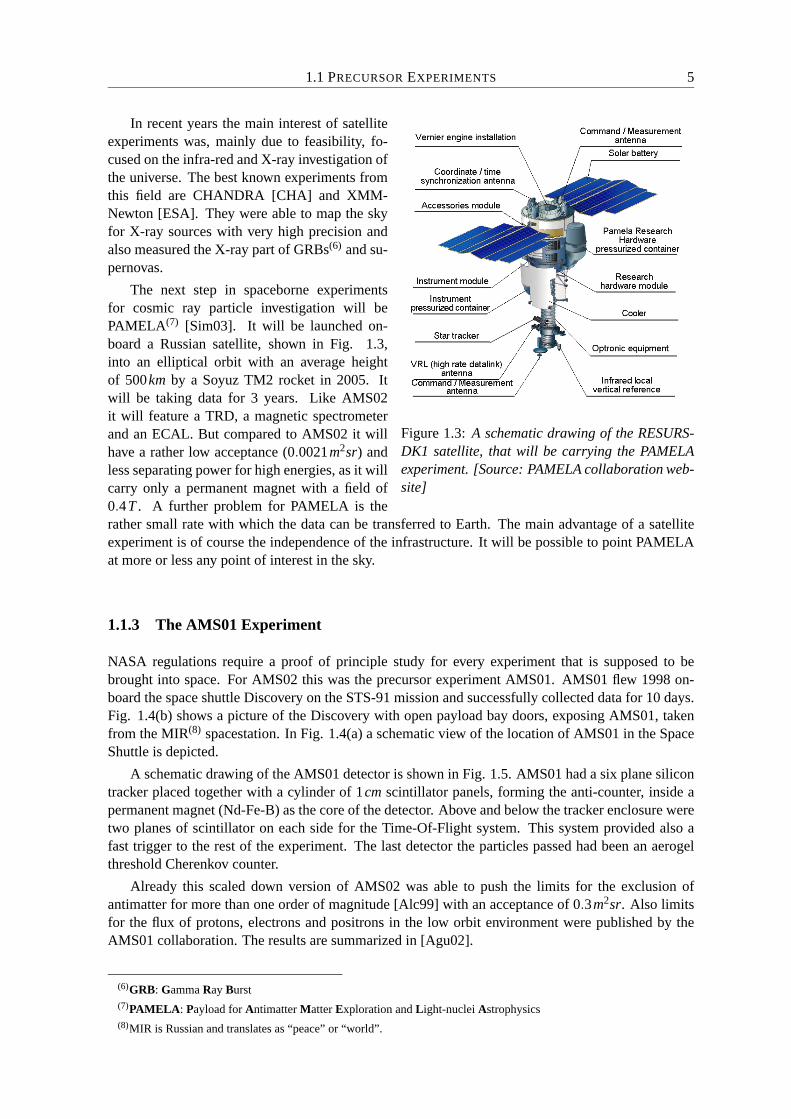
Figure 1.3: A schematic drawing of the RESURS-DK1 satellite, that will be carrying the PAMELAexperiment. [Source: PAMELA collaboration web-site]
In recent years the main interest of satelliteexperiments was, mainly due to feasibility, fo-cused on the infra-red and X-ray investigation ofthe universe. The best known experiments fromthis field are CHANDRA [CHA] and XMM-Newton [ESA]. They were able to map the skyfor X-ray sources with very high precision andalso measured the X-ray part of GRBs(6) and su-pernovas.
The next step in spaceborne experimentsfor cosmic ray particle investigation will bePAMELA(7) [Sim03]. It will be launched on-board a Russian satellite, shown in Fig. 1.3,into an elliptical orbit with an average heightof 500km by a Soyuz TM2 rocket in 2005. Itwill be taking data for 3 years. Like AMS02it will feature a TRD, a magnetic spectrometerand an ECAL. But compared to AMS02 it willhave a rather low acceptance (0.0021m2sr) andless separating power for high energies, as it willcarry only a permanent magnet with a field of0.4T . A further problem for PAMELA is therather small rate with which the data can be transferred to Earth. The main advantage of a satelliteexperiment is of course the independence of the infrastructure. It will be possible to point PAMELAat more or less any point of interest in the sky.
1.1.3 The AMS01 Experiment
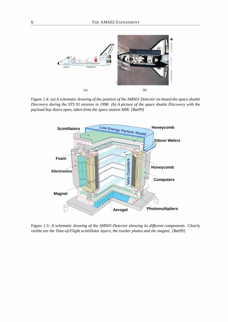
NASA regulations require a proof of principle study for every experiment that is supposed to bebrought into space. For AMS02 this was the precursor experiment AMS01. AMS01 flew 1998 on-board the space shuttle Discovery on the STS-91 mission and successfully collected data for 10 days.Fig. 1.4(b) shows a picture of the Discovery with open payload bay doors, exposing AMS01, takenfrom the MIR(8) spacestation. In Fig. 1.4(a) a schematic view of the location of AMS01 in the SpaceShuttle is depicted.
A schematic drawing of the AMS01 detector is shown in Fig. 1.5. AMS01 had a six plane silicontracker placed together with a cylinder of 1cm scintillator panels, forming the anti-counter, inside apermanent magnet (Nd-Fe-B) as the core of the detector. Above and below the tracker enclosure weretwo planes of scintillator on each side for the Time-Of-Flight system. This system provided also afast trigger to the rest of the experiment. The last detector the particles passed had been an aerogelthreshold Cherenkov counter.
Already this scaled down version of AMS02 was able to push the limits for the exclusion ofantimatter for more than one order of magnitude [Alc99] with an acceptance of 0.3m2sr. Also limitsfor the flux of protons, electrons and positrons in the low orbit environment were published by theAMS01 collaboration. The results are summarized in [Agu02].
(6)GRB: Gamma Ray Burst(7)PAMELA: Payload for Antimatter Matter Exploration and Light-nuclei Astrophysics(8)MIR is Russian and translates as “peace” or “world”.
6 THE AMS02 EXPERIMENT
Payloads
1 2 3 4 5 6 7 8 9 10 11 12 13
OV-103
NASA
AMS
Discovery
SM-Spacehab
(a) (b)
Figure 1.4: (a) A schematic drawing of the position of the AMS01 Detector on-board the space shuttleDiscovery during the STS 91 mission in 1998. (b) A picture of the space shuttle Discovery with thepayload bay doors open, taken from the space station MIR. [Bat99]
Honeycomb
Silicon Wafers
Honeycomb
Computers
PhotomultipliersAerogel
Magnet
Electronics
Foam
Scintillators Low Energy Particle Shield
Vet
o C
ou
nte
rs
Figure 1.5: A schematic drawing of the AMS01-Detector showing its different components. Clearlyvisible are the Time-of-Flight scintillator layers, the tracker planes and the magnet. [Bat99]
1.2 THE AMS02 DETECTOR 7
1.2 The AMS02 Detector
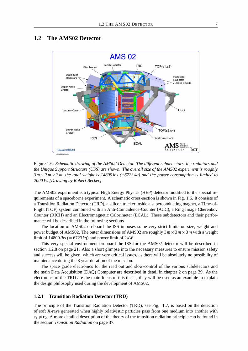
Figure 1.6: Schematic drawing of the AMS02 Detector. The different subdetectors, the radiators andthe Unique Support Structure (USS) are shown. The overall size of the AMS02 experiment is roughly3m× 3m× 3m, the total weight is 14809 lbs (=6723 kg) and the power consumption is limited to2000 W. [Drawing by Robert Becker]
The AMS02 experiment is a typical High Energy Physics (HEP) detector modified to the special re-quirements of a spaceborne experiment. A schematic cross-section is shown in Fig. 1.6. It consists ofa Transition Radiation Detector (TRD), a silicon tracker inside a superconducting magnet, a Time-of-Flight (TOF) system combined with an Anti-Coincidence-Counter (ACC), a Ring Image CherenkovCounter (RICH) and an Electromagnetic Calorimeter (ECAL). These subdetectors and their perfor-mance will be described in the following sections.
The location of AMS02 on-board the ISS imposes some very strict limits on size, weight andpower budget of AMS02. The outer dimensions of AMS02 are roughly 3m×3m×3m with a weightlimit of 14809 lbs (= 6723kg) and power limit of 2kW .
This very special environment on-board the ISS for the AMS02 detector will be described insection 1.2.8 on page 21. Also a short glimpse into the necessary measures to ensure mission safetyand success will be given, which are very critical issues, as there will be absolutely no possibility ofmaintenance during the 3 year duration of the mission.
The space grade electronics for the read out and slow-control of the various subdetectors andthe main Data Acquisition (DAQ) Computer are described in detail in chapter 2 on page 39. As theelectronics of the TRD are the main focus of this thesis, they will be used as an example to explainthe design philosophy used during the development of AMS02.
1.2.1 Transition Radiation Detector (TRD)
The principle of the Transition Radiation Detector (TRD), see Fig. 1.7, is based on the detectionof soft X-rays generated when highly relativistic particles pass from one medium into another withε1 = ε2. A more detailed description of the theory of the transition radiation principle can be found inthe section Transition Radiation on page 37.
8 THE AMS02 EXPERIMENT
As the probability of the emission of a gamma quant is rather low for one transition (∼ 10−2),the radiator material is composed of a so-called fleece (ρ = 0.06g/cm−3), which is made of very thinfibres (10µm), thus increasing the number of transitions per layer. The gamma quants are detectedby proportional gas counters. The voltage applied between the central wire and the tube walls is∼ 1600V . The gas mixture used for the TRD of AMS02 is Xe : CO2 80:20. In this mixture the Xe isthe gas interacting with the particles (high Z), while the CO2 absorbs the UV light emitted from theexcited Xe-ions, thus preventing avalanche break-downs. The probability to detect one of the photonsgenerated by the passing particle is ∼ 50%.
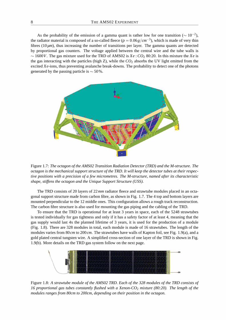
Figure 1.7: The octagon of the AMS02 Transition Radiation Detector (TRD) and the M-structure. Theoctagon is the mechanical support structure of the TRD. It will keep the detector tubes at their respec-tive positions with a precision of a few micrometres. The M-structure, named after its characteristicshape, stiffens the octagon and the Unique Support Structure (USS).
The TRD consists of 20 layers of 22mm radiator fleece and strawtube modules placed in an octa-gonal support structure made from carbon fibre, as shown in Fig. 1.7. The 4 top and bottom layers aremounted perpendicular to the 12 middle ones. This configuration allows a rough track reconstruction.The carbon fibre structure is also used for mounting the gas piping and the cabling of the TRD.
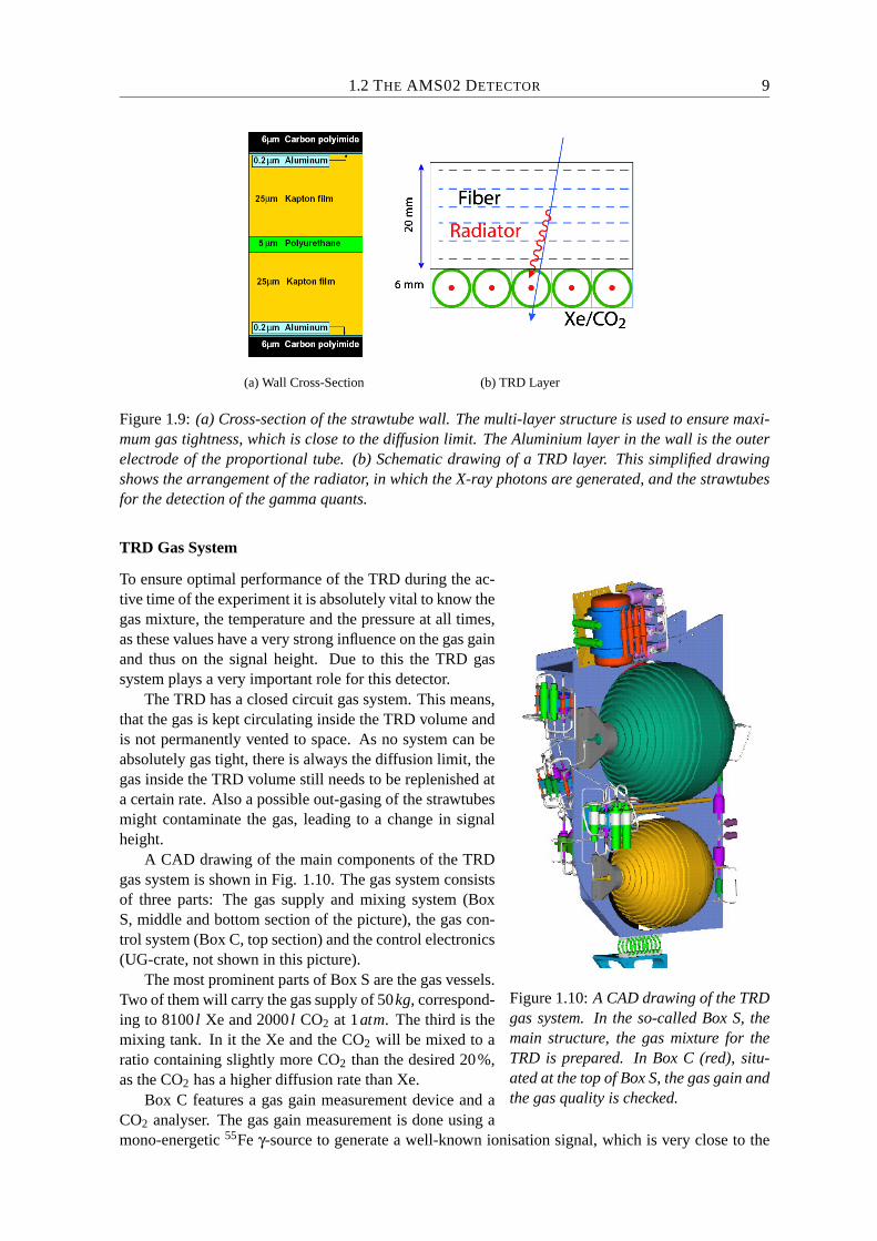
To ensure that the TRD is operational for at least 3 years in space, each of the 5248 strawtubesis tested individually for gas tightness and only if it has a safety factor of at least 4, meaning that thegas supply would last 4x the planned lifetime of 3 years, it is used for the production of a module(Fig. 1.8). There are 328 modules in total, each module is made of 16 strawtubes. The length of themodules varies from 80cm to 200cm. The strawtubes have walls of Kapton foil, see Fig. 1.9(a), and agold plated central tungsten wire. A simplified cross-section of one layer of the TRD is shown in Fig.1.9(b). More details on the TRD gas system follow on the next page.
Figure 1.8: A strawtube module of the AMS02 TRD. Each of the 328 modules of the TRD consists of16 proportional gas tubes constantly flushed with a Xenon-CO2 mixture (80:20). The length of themodules ranges from 80cm to 200cm, depending on their position in the octagon.
1.2 THE AMS02 DETECTOR 9
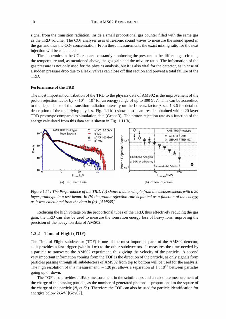
(a) Wall Cross-Section (b) TRD Layer
Figure 1.9: (a) Cross-section of the strawtube wall. The multi-layer structure is used to ensure maxi-mum gas tightness, which is close to the diffusion limit. The Aluminium layer in the wall is the outerelectrode of the proportional tube. (b) Schematic drawing of a TRD layer. This simplified drawingshows the arrangement of the radiator, in which the X-ray photons are generated, and the strawtubesfor the detection of the gamma quants.
TRD Gas System
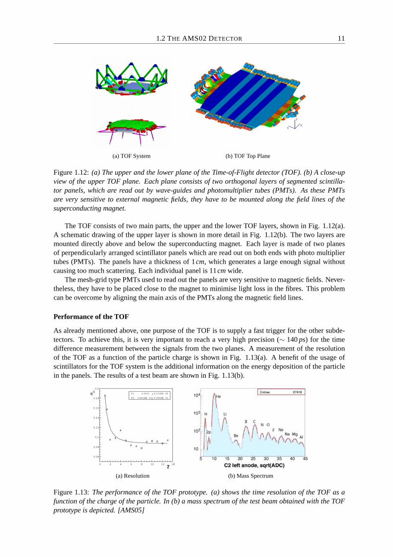
Figure 1.10: A CAD drawing of the TRDgas system. In the so-called Box S, themain structure, the gas mixture for theTRD is prepared. In Box C (red), situ-ated at the top of Box S, the gas gain andthe gas quality is checked.
To ensure optimal performance of the TRD during the ac-tive time of the experiment it is absolutely vital to know thegas mixture, the temperature and the pressure at all times,as these values have a very strong influence on the gas gainand thus on the signal height. Due to this the TRD gassystem plays a very important role for this detector.
The TRD has a closed circuit gas system. This means,that the gas is kept circulating inside the TRD volume andis not permanently vented to space. As no system can beabsolutely gas tight, there is always the diffusion limit, thegas inside the TRD volume still needs to be replenished ata certain rate. Also a possible out-gasing of the strawtubesmight contaminate the gas, leading to a change in signalheight.
A CAD drawing of the main components of the TRDgas system is shown in Fig. 1.10. The gas system consistsof three parts: The gas supply and mixing system (BoxS, middle and bottom section of the picture), the gas con-trol system (Box C, top section) and the control electronics(UG-crate, not shown in this picture).
The most prominent parts of Box S are the gas vessels.Two of them will carry the gas supply of 50kg, correspond-ing to 8100 l Xe and 2000 l CO2 at 1atm. The third is themixing tank. In it the Xe and the CO2 will be mixed to aratio containing slightly more CO2 than the desired 20%,as the CO2 has a higher diffusion rate than Xe.
Box C features a gas gain measurement device and aCO2 analyser. The gas gain measurement is done using amono-energetic 55Fe γ-source to generate a well-known ionisation signal, which is very close to the
10 THE AMS02 EXPERIMENT
signal from the transition radiation, inside a small proportional gas counter filled with the same gasas the TRD volume. The CO2 analyser uses ultra-sonic sound waves to measure the sound speed inthe gas and thus the CO2 concentration. From these measurements the exact mixing ratio for the nextinjection will be calculated.
The electronics in the UG crate are constantly monitoring the pressure in the different gas circuits,the temperature and, as mentioned above, the gas gain and the mixture ratio. The information of thegas pressure is not only used for the physics analysis, but it is also vital for the detector, as in case ofa sudden pressure drop due to a leak, valves can close off that section and prevent a total failure of theTRD.
Performance of the TRD
The most important contribution of the TRD to the physics data of AMS02 is the improvement of theproton rejection factor by ∼ 102 −103 for an energy range of up to 300GeV . This can be accreditedto the dependence of the transition radiation intensity on the Lorentz factor γ, see 1.3.6 for detaileddescription of the underlying physics. Fig. 1.11(a) shows test beam results obtained with a 20 layerTRD prototype compared to simulation data (Geant 3). The proton rejection rate as a function of theenergy calculated from this data set is shown in Fig. 1.11(b).
(a) Test Beam Data (b) Proton Rejection
Figure 1.11: The Performance of the TRD. (a) shows a data sample from the measurements with a 20layer prototype in a test beam. In (b) the proton rejection rate is plotted as a function of the energy,as it was calculated from the data in (a). [AMS05]
Reducing the high voltage on the proportional tubes of the TRD, thus effectively reducing the gasgain, the TRD can also be used to measure the ionisation energy loss of heavy ions, improving theprecision of the heavy ion data of AMS02.
1.2.2 Time of Flight (TOF)
The Time-of-Flight subdetector (TOF) is one of the most important parts of the AMS02 detector,as it provides a fast trigger (within 1µs) to the other subdetectors. It measures the time needed bya particle to transverse the AMS02 experiment, thus giving the velocity of the particle. A secondvery important information coming from the TOF is the direction of the particle, as only signals fromparticles passing through all subdetectors of AMS02 from top to bottom will be used for the analysis.The high resolution of this measurement, ∼ 120 ps, allows a separation of 1 : 1011 between particlesgoing up or down.
The TOF also provides a dE/dx measurement in the scintillators and an absolute measurement ofthe charge of the passing particle, as the number of generated photons is proportional to the square ofthe charge of the particle (Nγ ∝ Z2). Therefore the TOF can also be used for particle identification forenergies below 2GeV [Goy02].
1.2 THE AMS02 DETECTOR 11
(a) TOF System (b) TOF Top Plane
Figure 1.12: (a) The upper and the lower plane of the Time-of-Flight detector (TOF). (b) A close-upview of the upper TOF plane. Each plane consists of two orthogonal layers of segmented scintilla-tor panels, which are read out by wave-guides and photomultiplier tubes (PMTs). As these PMTsare very sensitive to external magnetic fields, they have to be mounted along the field lines of thesuperconducting magnet.
The TOF consists of two main parts, the upper and the lower TOF layers, shown in Fig. 1.12(a).A schematic drawing of the upper layer is shown in more detail in Fig. 1.12(b). The two layers aremounted directly above and below the superconducting magnet. Each layer is made of two planesof perpendicularly arranged scintillator panels which are read out on both ends with photo multipliertubes (PMTs). The panels have a thickness of 1cm, which generates a large enough signal withoutcausing too much scattering. Each individual panel is 11cm wide.
The mesh-grid type PMTs used to read out the panels are very sensitive to magnetic fields. Never-theless, they have to be placed close to the magnet to minimise light loss in the fibres. This problemcan be overcome by aligning the main axis of the PMTs along the magnetic field lines.
Performance of the TOF
As already mentioned above, one purpose of the TOF is to supply a fast trigger for the other subde-tectors. To achieve this, it is very important to reach a very high precision (∼ 140 ps) for the timedifference measurement between the signals from the two planes. A measurement of the resolutionof the TOF as a function of the particle charge is shown in Fig. 1.13(a). A benefit of the usage ofscintillators for the TOF system is the additional information on the energy deposition of the particlein the panels. The results of a test beam are shown in Fig. 1.13(b).
20
23
0.1631 0.1194E 02
0.8614E 01
0.06
0.08
0.1
0.12
0.14
0.16
0.18
0 2 4 6 8 10 12 1
P1 ±
P2 0.7259E 03±
(a) Resolution (b) Mass Spectrum
Figure 1.13: The performance of the TOF prototype. (a) shows the time resolution of the TOF as afunction of the charge of the particle. In (b) a mass spectrum of the test beam obtained with the TOFprototype is depicted. [AMS05]

12 THE AMS02 EXPERIMENT
1.2.3 Silicon Tracker
The silicon tracker is the central part of the AMS02 experiment. It consists of eight layers arrangedin five planes inside the superconducting magnet, see Fig. 1.14. Each plane is made of a carbon fibrehoneycomb structure to which the so-called ladders with double-sided silicon detectors are mounted.While the top and the bottom plane have one layer of silicon detectors, the middle planes feature twolayers each with a total sensitive area of 6.6m2.
There are 7 to 15 sensors on each of the 192 ladders, which are wrapped in an EMI(9) shielding.The ladders are mounted head to head on the planes, see Fig. 1.15(a). The front-end electronics areplaced on the thermal bars at the end of each ladder. A picture of a ladder is shown in Fig. 1.15(b).
Figure 1.14: The Silicon Tracker. The tracker, with a total sensitive area of 6.6m2, consists of 8layers, which are arranged in five planes. The top and bottom planes consist of one layer of siliconeach, while the middle planes consist of two.
The silicon detectors used in the AMS02 tracker are double sided strip detectors with a positionresolution of 10µm in the bending plane of the magnet and 20µm in the non-bending. The strips onthe two sides of the silicon are perpendicular to each other to allow for a two-dimensional positionmeasurement in each layer. The thickness of the silicon is 300µm. The nominal bias voltage for thesilicon detectors is ∼ 80V .
To ensure the maximal position resolution during all run conditions a so-called Tracker AlignmentSystem is used to monitor the relative position of the 8 tracker planes. This system is using the partialtransparency of crystalline silicon for infra-red light to shine an IR laser through so-called AlignmentHoles in all planes. Thus a signal is generated in all planes and the track can be reconstructed, definingthe relative position of the planes. The system consists of 5 pairs located in the centre of the tracker.
Due to improvements in the sensor design and the higher magnetic field, the performance of theAMS02 tracker will exceed the one of its predecessor by far. It will be able to measure the rigidity
(9)EMI: Electro-Magnetic Interference

1.2 THE AMS02 DETECTOR 13
up to a few tens of TeV . With the measurement of the specific energy loss it will be possible toidentify individual elements, as dE/dx ∼ |Z2|, for |Z2| ≤ 28. The tracker will also measure energyand direction of photons, which were converted in the material above.
(a) Tracker Plane 2 (b) Tracker Ladder
Figure 1.15: (a) Plane 2 of the tracker, with one side fully assembled with ladders. (b) One of theladders of the tracker during assembly, before the EMI shielding is mounted on the ladder.
Tracker Thermal Control System
The silicon tracker of AMS02 has by far the largest power budget of all subdetectors. In the normalrun mode it consumes 800W , most of this in its read out hybrids. To ensure stable operating conditionsfor the tracker, a thermal management is needed. The Tracker Thermal Control System (TTCS) is aclosed loop cooling system designed to keep the silicon detectors and the front-end hybrids withintheir optimal temperature range. It is depicted in Fig. 1.16. Especially for the detectors this is veryimportant, as the leakage current of the detectors, and thus the noise, scales exponentially with thetemperature.
Figure 1.16: The Tracker Thermal Control System (TTCS). The cooling pipes, the heat exchangersand the thermal bars, with which the heat is transferred from the ladders to the heat exchangers, areshown.
14 THE AMS02 EXPERIMENT
The heat generated by the silicon detectors and the front-end chips is brought via thermal barsto heat exchangers of the TTCS to keep the detector and its read out within the optimal temperaturerange. In these heat exchangers a part of the cooling liquid CO2 is evaporated. The two-phase mixtureof liquid and gas is then pumped to the condensers, another set of heat exchangers. These are mountedon the upper radiators on wake(10) and ram(11) side. Inserted into the radiators are heat-pipes, to ensurea homogenous temperature distribution over the radiators.
The Superconducting Magnet
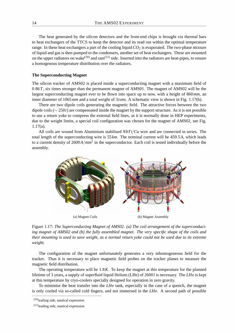
The silicon tracker of AMS02 is placed inside a superconducting magnet with a maximum field of0.86T , six times stronger than the permanent magnet of AMS01. The magnet of AMS02 will be thelargest superconducting magnet ever to be flown into space up to now, with a height of 860mm, aninner diameter of 1065mm and a total weight of 3 tons. A schematic view is shown in Fig. 1.17(b).
There are two dipole coils generating the magnetic field. The attractive forces between the twodipole coils (∼ 250 t) are compensated inside the magnet by the support structure. As it is not possibleto use a return yoke to compress the external field lines, as it is normally done in HEP experiments,due to the weight limits, a special coil configuration was chosen for the magnet of AMS02, see Fig.1.17(a).
All coils are wound from Aluminium stabilised NbTi/Cu wire and are connected in series. Thetotal length of the superconducting wire is 55km. The nominal current will be 459.5A, which leadsto a current density of 2600A/mm2 in the superconductor. Each coil is tested individually before theassembly.
(a) Magnet Coils (b) Magnet Assembly
Figure 1.17: The Superconducting Magnet of AMS02. (a) The coil arrangement of the superconduct-ing magnet of AMS02 and (b) the fully assembled magnet. The very specific shape of the coils andtheir mounting is used to save weight, as a normal return yoke could not be used due to its extremeweight.
The configuration of the magnet unfortunately generates a very inhomogeneous field for thetracker. Thus it is necessary to place magnetic field probes on the tracker planes to measure themagnetic field distribution.
The operating temperature will be 1.8K. To keep the magnet at this temperature for the plannedlifetime of 3 years, a supply of superfluid liquid Helium (LHe) of 2600 l is necessary. The LHe is keptat this temperature by cryo-coolers specially designed for operation in zero gravity.
To minimise the heat transfer into the LHe tank, especially in the case of a quench, the magnetis only cooled via so-called cold fingers, and not immersed in the LHe. A second path of possible
(10)trailing side, nautical expression(11)leading side, nautical expression
1.2 THE AMS02 DETECTOR 15
heat transfer is the mechanical fixation of the magnet. Therefore a new design is used to keep the heattransfer as small as possible while ensuring maximum safety for the magnet during launch: non-linearstraps. These straps are very strong and stiff in high load situations, like the launch, but they decouplethemselves during normal situations.
The magnet and the LHe tank are situated in a vacuum vessel. This vessel is of course onlynecessary for insulation during operation on ground, but in space it will also act as shield, to preventa puncture of the LHe vessel in case AMS02 is hit by micro-meteorites.
Due to the limitations in power consumption imposed on AMS02 by the ISS, a special procedureis needed to ramp up the magnetic field without exceeding a maximum power of 1850W . In thefirst stage of this process the voltage is limited, in the second part the power and in the final stagethe current. After the nominal current has been reached, a superconducting switch inside the magnetcomposure will decouple the magnet from the external supply and it will be operating in the persistentmode: the current will keep cycling in the coils without any connection to the outside. No externalpower will be needed to keep the magnet, which stores 5.15MJ when fully charged, in operation.
In the very unlikely case of a quench of one coil, all coils will be heated above TC to make sure,that the heat generated in the magnet will not fatally damage the quenching coil, but is spread over allcoils. The magnet system is designed in such a way, that after such an event AMS02 would be fullyoperational again after 3 days.
As the superconducting magnet is one of the most crucial items of the AMS02 experiment, it isprotected by an uninterruptible power supply (UPS), which allows to keep the magnet operational incase of a power loss on the ISS for up to 8 hours. If the nominal power is not restored within that timeframe, the magnet will be ramped down.
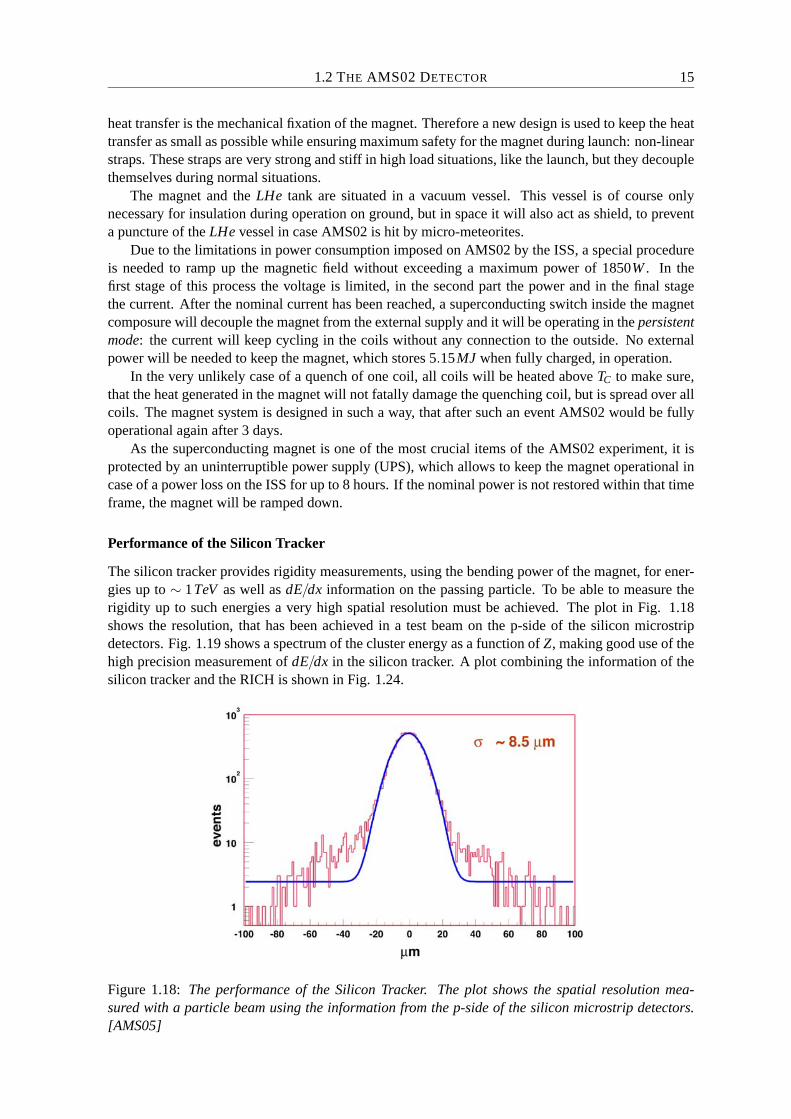
Performance of the Silicon Tracker
The silicon tracker provides rigidity measurements, using the bending power of the magnet, for ener-gies up to ∼ 1TeV as well as dE/dx information on the passing particle. To be able to measure therigidity up to such energies a very high spatial resolution must be achieved. The plot in Fig. 1.18shows the resolution, that has been achieved in a test beam on the p-side of the silicon microstripdetectors. Fig. 1.19 shows a spectrum of the cluster energy as a function of Z, making good use of thehigh precision measurement of dE/dx in the silicon tracker. A plot combining the information of thesilicon tracker and the RICH is shown in Fig. 1.24.
Figure 1.18: The performance of the Silicon Tracker. The plot shows the spatial resolution mea-sured with a particle beam using the information from the p-side of the silicon microstrip detectors.[AMS05]
16 THE AMS02 EXPERIMENT
Figure 1.19: The performance of the Silicon Tracker. The plot shows a spectrum of the cluster energyas a function of Z. [AMS05]
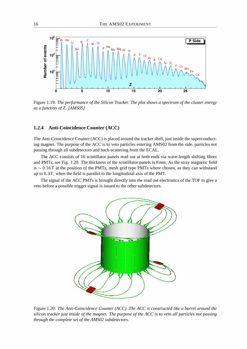
1.2.4 Anti-Coincidence Counter (ACC)
The Anti-Coincidence Counter (ACC) is placed around the tracker shell, just inside the superconduct-ing magnet. The purpose of the ACC is to veto particles entering AMS02 from the side, particles notpassing through all subdetectors and back-scattering from the ECAL.
The ACC consists of 16 scintillator panels read out at both ends via wave-length shifting fibresand PMTs, see Fig. 1.20. The thickness of the scintillator panels is 8mm. As the stray magnetic fieldis ∼ 0.16T at the position of the PMTs, mesh grid type PMTs where chosen, as they can withstandup to 0.3T , when the field is parallel to the longitudinal axis of the PMT.
The signal of the ACC PMTs is brought directly into the read out electronics of the TOF to give aveto before a possible trigger signal is issued to the other subdetectors.
Figure 1.20: The Anti-Coincidence Counter (ACC). The ACC is constructed like a barrel around thesilicon tracker just inside of the magnet. The purpose of the ACC is to veto all particles not passingthrough the complete set of the AMS02 subdetectors.
1.2 THE AMS02 DETECTOR 17
Performance of the ACC
The most important characteristic of the ACC is its inefficiency. As its purpose is to veto all particlesthat are not passing through the complete set of AMS02 subdetectors, it is important, that it recognisesall particles hitting its panels. This was extensively tested with a 10GeV particle beam. In Fig. 1.21the pulse height spectrum is plotted on the left and the counts vs. charge for different trigger settingson the right.
Figure 1.21: The performance of the ACC. The plot on the left shows a pulse height distribution for a10GeV particle beam. (b) shows the counts vs. charge for different trigger settings. [AMS05]
1.2.5 Ring Image Cherenkov Counter (RICH)
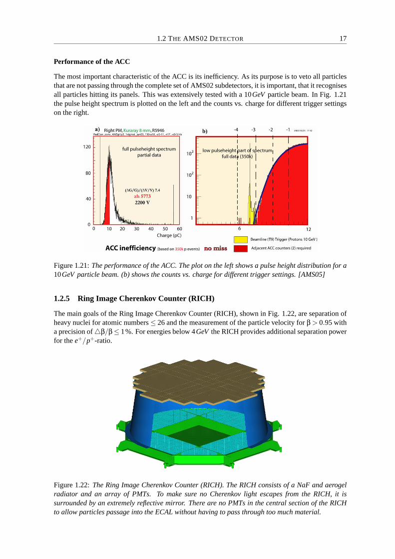
The main goals of the Ring Image Cherenkov Counter (RICH), shown in Fig. 1.22, are separation ofheavy nuclei for atomic numbers ≤ 26 and the measurement of the particle velocity for β > 0.95 witha precision of β/β ≤ 1%. For energies below 4GeV the RICH provides additional separation powerfor the e+/p+-ratio.
Figure 1.22: The Ring Image Cherenkov Counter (RICH). The RICH consists of a NaF and aerogelradiator and an array of PMTs. To make sure no Cherenkov light escapes from the RICH, it issurrounded by an extremely reflective mirror. There are no PMTs in the central section of the RICHto allow particles passage into the ECAL without having to pass through too much material.
18 THE AMS02 EXPERIMENT
The RICH consists of three main parts: The radiator plane, the drift space and the detection plane.The radiator plane is made from NaF and aerogel tiles with a thickness of 30mm and a refractiveindex n = 1.03− 1.05, embedded in an aluminium frame. The drift space has a length of 414mmand is surrounded by an extremely reflective mirror, to make sure that no section of the CherenkovRing escapes from the detector. The detection plane is composed of 680 sensitive elements. Each ofthese elements consists of a segmented 4×4 light guide cone and a pixelated PMT. The central area(64×64cm2) of the detection plane is not equipped with PMTs to allow particles passage through theRICH into the ECAL with minimal interaction probability.
From the spatial coordinates of the PMTs, the signal height and the incoming track position theCherenkov cone is calculated. The opening angle of the cone determines the velocity of the incomingparticle. The accuracy of this measurement is σβ/β ≈ 10−3. The intensity of the light detected givesan estimation on the charge of the particle. This was proven in a test beam for Z up to 40.
Performance of the RICH
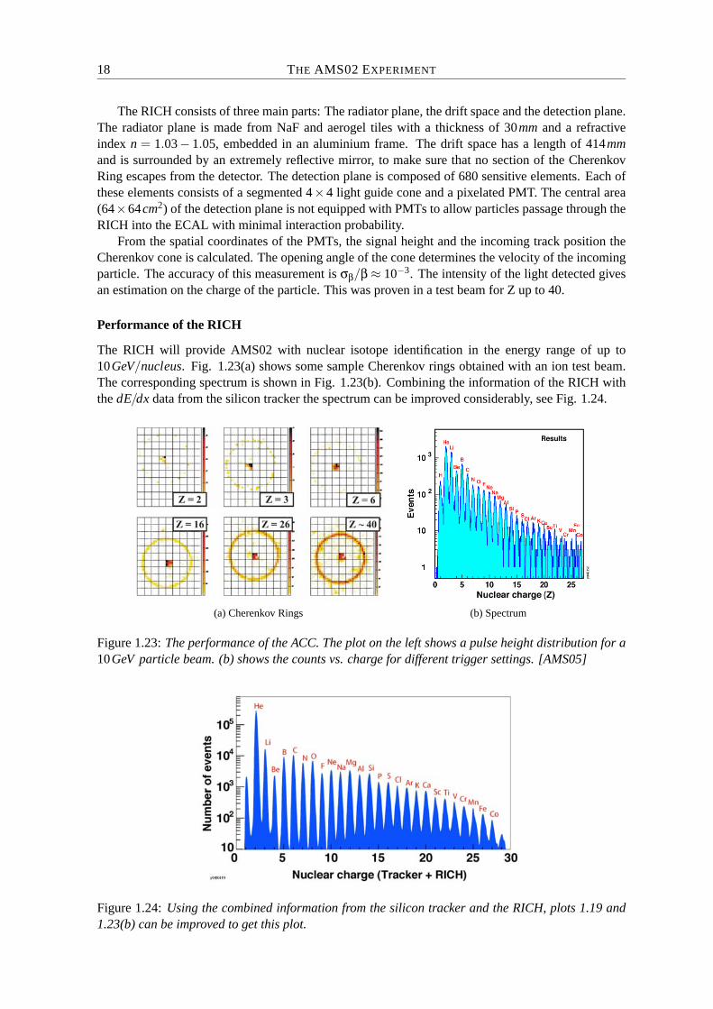
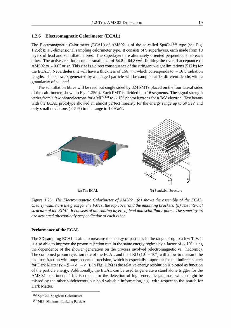
The RICH will provide AMS02 with nuclear isotope identification in the energy range of up to10GeV/nucleus. Fig. 1.23(a) shows some sample Cherenkov rings obtained with an ion test beam.The corresponding spectrum is shown in Fig. 1.23(b). Combining the information of the RICH withthe dE/dx data from the silicon tracker the spectrum can be improved considerably, see Fig. 1.24.
(a) Cherenkov Rings (b) Spectrum
Figure 1.23: The performance of the ACC. The plot on the left shows a pulse height distribution for a10GeV particle beam. (b) shows the counts vs. charge for different trigger settings. [AMS05]
Figure 1.24: Using the combined information from the silicon tracker and the RICH, plots 1.19 and1.23(b) can be improved to get this plot.
1.2 THE AMS02 DETECTOR 19
1.2.6 Electromagnetic Calorimeter (ECAL)
The Electromagnetic Calorimeter (ECAL) of AMS02 is of the so-called SpaCal(12) type (see Fig.1.25(b)), a 3-dimensional sampling calorimeter type. It consists of 9 superlayers, each made from 10layers of lead and scintillator fibres. The superlayers are alternately oriented perpendicular to eachother. The active area has a rather small size of 64.8× 64.8cm2, limiting the overall acceptance ofAMS02 to ∼ 0.05m2sr. This size is a direct consequence of the stringent weight limitations (512kg forthe ECAL). Nevertheless, it will have a thickness of 166mm, which corresponds to ∼ 16.5 radiationlengths. The showers generated by a charged particle will be sampled at 18 different depths with agranularity of ∼ 1cm3.
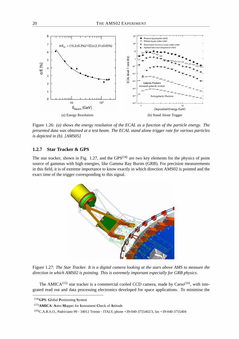
The scintillation fibres will be read out single sided by 324 PMTs placed on the four lateral sidesof the calorimeter, shown in Fig. 1.25(a). Each PMT is divided into 16 segments. The signal strengthvaries from a few photoelectrons for a MIP(13) to ∼ 105 photoelectrons for a TeV electron. Test beamswith the ECAL prototype showed an almost perfect linearity for the energy range up to 50GeV andonly small deviations (< 5%) in the range to 180GeV .
(a) The ECAL (b) Sandwich Structure
Figure 1.25: The Electromagnetic Calorimeter of AMS02. (a) shows the assembly of the ECAL.Clearly visible are the grids for the PMTs, the top cover and the mounting brackets. (b) The internalstructure of the ECAL. It consists of alternating layers of lead and scintillator fibres. The superlayersare arranged alternatingly perpendicular to each other.
Performance of the ECAL
The 3D sampling ECAL is able to measure the energy of particles in the range of up to a few TeV. Itis also able to improve the proton rejection rate in the same energy regime by a factor of ∼ 103 usingthe dependence of the shower generation on the process involved (electromagnetic vs. hadronic).The combined proton rejection rate of the ECAL and the TRD (105 −106) will allow to measure thepositron fraction with unprecedented precision, which is especially important for the indirect searchfor Dark Matter (χ+χ → e−+e+). In Fig. 1.26(a) the relative energy resolution is plotted as functionof the particle energy. Additionally, the ECAL can be used to generate a stand alone trigger for theAMS02 experiment. This is crucial for the detection of high energetic gammas, which might bemissed by the other subdetectors but hold valuable information, e.g. with respect to the search forDark Matter.
(12)SpaCal: Spaghetti Calorimeter(13)MIP: Minimum Ionizing Particle
20 THE AMS02 EXPERIMENT
(a) Energy Resolution (b) Stand Alone Trigger
Figure 1.26: (a) shows the energy resolution of the ECAL as a function of the particle energy. Thepresented data was obtained at a test beam. The ECAL stand alone trigger rate for various particlesis depicted in (b). [AMS05]
1.2.7 Star Tracker & GPS
The star tracker, shown in Fig. 1.27, and the GPS(14) are two key elements for the physics of pointsource of gammas with high energies, like Gamma Ray Bursts (GRB). For precision measurementsin this field, it is of extreme importance to know exactly in which direction AMS02 is pointed and theexact time of the trigger corresponding to this signal.
Figure 1.27: The Star Tracker. It is a digital camera looking at the stars above AMS to measure thedirection in which AMS02 is pointing. This is extremely important especially for GRB physics.
The AMICA(15) star tracker is a commercial cooled CCD camera, made by Carso(16), with inte-grated read out and data processing electronics developed for space applications. To minimise the
(14)GPS: Global Positioning System(15)AMICA: Astro Mapper for Instrument Check of Attitude(16)C.A.R.S.O., Padriciano 99 - 34012 Trieste - ITALY, phone +39-040-3755402/3, fax +39-040-3755404
1.2 THE AMS02 DETECTOR 21
necessary amount of data to be transferred to the main computers of AMS02, these electronics arecapable of calculating the direction by comparing the actual picture taken with a database of star po-sitions in the sky. The AMICA star tracker is derived from the UVSTAR(17) telescope, that was flownthree times successfully on the space shuttle.
The GPS system for AMS02 is also based on a commercially available GPS receiver, the Topstar3000D by Alcatel. It will deliver a time stamp to the electronics of the star tracker with a rate of∼ 1kHz.
Performance of the Star Tracker & the GPS
The Star Tracker and the GPS play a very important role in the search for point-like sources of highenergy gammas. Their combined information allows to measure the orientation of AMS02 with aprecision in the arcsecond range. Additionally, a time profile of the event can be established. Can-didates for point-like sources of high energy gammas are the Dark Matter Annihilation in galactic orextragalactic sources, GRBs, Pulsars, Active Galactic Nuclei and possible exotic events. The AMS02experiment can detect gammas in the energy range of 10− 100GeV , either by conversion in one ofthe top layers of the TRD or by an electromagnetic cascade in the ECAL.
1.2.8 Detector Environment
One of the main challenges of the AMS02 project is to build a High Energy Physics high precisiondetector that can withstand the vibrations during the launch and the harsh environment in space.
The vibrations during the launch and the re-entry into Earth’s atmosphere can exert forces of upto 6.8g onto the detector. Additionally, the NASA requires, that the first significant eigenfrequency ofany device flown on-board a space shuttle has to be above 50Hz to prevent catastrophic resonances. Asthe detector should keep its precision alignment even during such extreme loads it is very importantto test all components and the whole experiment for their behaviour under vibration. The standardprocedure for this is the usage of finite element simulations and measurements on shaker tables toverify these simulations. This approach is also applied by the AMS02 collaboration.
As the orbit of the ISS has a height of ∼ 400km, the space station is on the outer fringes ofEarth’s atmosphere. The remanent outside pressure at the height of the ISS is 1.45 × 10⁻⁸ mbar[Pet03]. This low pressure is in itself already a technical challenge, but even more demanding is thefast transition from normal pressure on the ground to the vacuum in space during the launch. Thedesign of all subdetectors has to allow the air trapped inside to escape rather fast without damagingthe detector. This is especially difficult for the silicon tracker, which has a large volume but should beabsolutely light tight, as any light entering the tracker would disturb its performance. In addition allcomponents and materials used in the construction of AMS02 have to be approved by NASA to meettheir requirements on out-gasing.
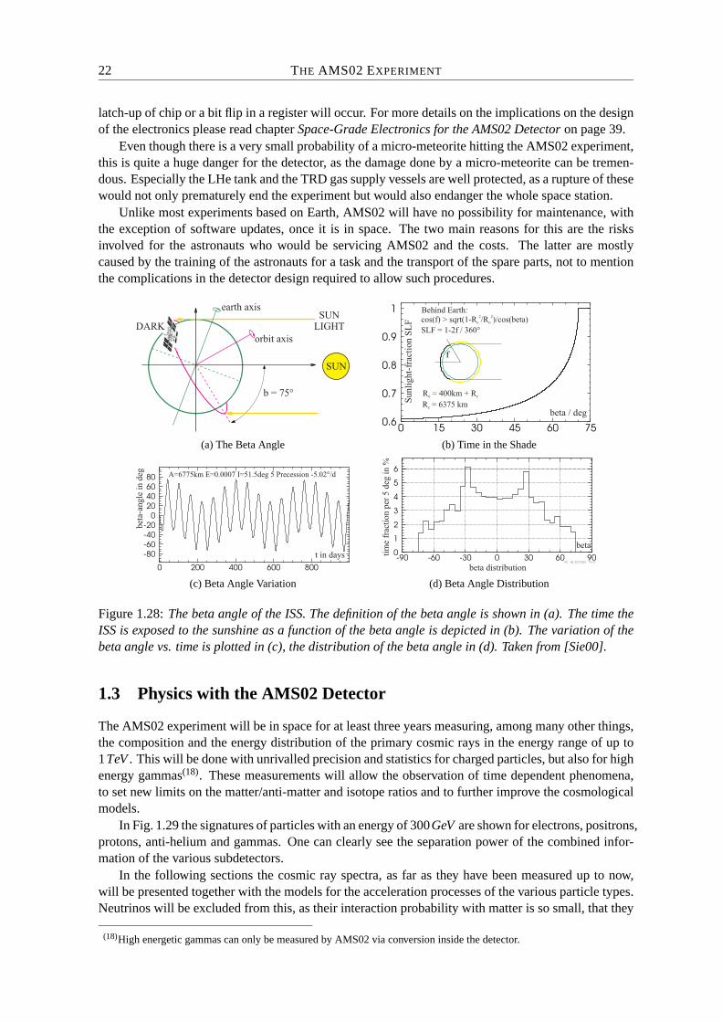
Temperatures in space can vary quite strongly from sunshine to shade. Therefore it is very impor-tant to calculate the time the detector spends in both, see Fig. 1.28. From this, one can compute thetemperature distribution the detector will see during its lifetime. It has to be ensured that all detectorcomponents can survive this temperature range non-operating and can be active in at least 90% ofit. This is especially demanding for the TRD and the read out electronics. As the TRD is a gaseousdetector it is very sensitive to temperature variations and the design goal is to keep temperature vari-ations inside the TRD below 0.5 C. For the read out electronics the issue is the cooling during theoperation. As there is no air available for convective cooling all heat transport has to be done bythermal conductivity. The heat is then dissipated into space by radiation.
Another issue, mainly for the electronics, is the damage done by the cosmic rays. While the totaldose expected is quite low, in the range of ∼ 1krad/yr, there is probability of a so-called Single EventUpset (SEU) caused by a heavy ion depositing so much charge in a silicon device, that, for example, a
(17)UVSTAR: Ultraviolet Spectrograph Telescope for Astronomical Research
22 THE AMS02 EXPERIMENT
latch-up of chip or a bit flip in a register will occur. For more details on the implications on the designof the electronics please read chapter Space-Grade Electronics for the AMS02 Detector on page 39.
Even though there is a very small probability of a micro-meteorite hitting the AMS02 experiment,this is quite a huge danger for the detector, as the damage done by a micro-meteorite can be tremen-dous. Especially the LHe tank and the TRD gas supply vessels are well protected, as a rupture of thesewould not only prematurely end the experiment but would also endanger the whole space station.
Unlike most experiments based on Earth, AMS02 will have no possibility for maintenance, withthe exception of software updates, once it is in space. The two main reasons for this are the risksinvolved for the astronauts who would be servicing AMS02 and the costs. The latter are mostlycaused by the training of the astronauts for a task and the transport of the spare parts, not to mentionthe complications in the detector design required to allow such procedures.
DARK
earth axis
orbit axis
SUNLIGHT
SUN
b = 75°
(a) The Beta Angle
0 15 30 45 60 75
f
Su
nli
gh
t-fr
acti
on
SL
Fbeta / deg
Behind Earth:cos(f) > sqrt(1-R /R )/cos(beta)e o
2 2
SLF = 1-2f / 360°
R = 400km + Ro e
R = 6375 kme
(b) Time in the Shade
40
60
80
0 200 400 600 800
bet
a-an
gle
indeg
t in days
A=6775km E=0.0007 I=51.5deg 5 Precession -5.02°/d
(c) Beta Angle Variation
0
1
2
3
4
5
6
-90 -60 -30 0 30 60 90
tim
efr
acti
on
per
5deg
in%
beta distribution
beta
(d) Beta Angle Distribution
Figure 1.28: The beta angle of the ISS. The definition of the beta angle is shown in (a). The time theISS is exposed to the sunshine as a function of the beta angle is depicted in (b). The variation of thebeta angle vs. time is plotted in (c), the distribution of the beta angle in (d). Taken from [Sie00].
1.3 Physics with the AMS02 Detector
The AMS02 experiment will be in space for at least three years measuring, among many other things,the composition and the energy distribution of the primary cosmic rays in the energy range of up to1TeV . This will be done with unrivalled precision and statistics for charged particles, but also for highenergy gammas(18). These measurements will allow the observation of time dependent phenomena,to set new limits on the matter/anti-matter and isotope ratios and to further improve the cosmologicalmodels.
In Fig. 1.29 the signatures of particles with an energy of 300GeV are shown for electrons, positrons,protons, anti-helium and gammas. One can clearly see the separation power of the combined infor-mation of the various subdetectors.
In the following sections the cosmic ray spectra, as far as they have been measured up to now,will be presented together with the models for the acceleration processes of the various particle types.Neutrinos will be excluded from this, as their interaction probability with matter is so small, that they
(18)High energetic gammas can only be measured by AMS02 via conversion inside the detector.
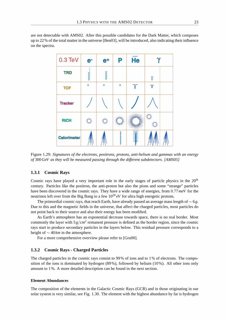
1.3 PHYSICS WITH THE AMS02 DETECTOR 23
are not detectable with AMS02. After this possible candidates for the Dark Matter, which composesup to 22% of the total matter in the universe [Ben03], will be introduced, also indicating their influenceon the spectra.
Figure 1.29: Signatures of the electrons, positrons, protons, anti-helium and gammas with an energyof 300GeV as they will be measured passing through the different subdetectors. [AMS05]
1.3.1 Cosmic Rays
Cosmic rays have played a very important role in the early stages of particle physics in the 20th
century. Particles like the positron, the anti-proton but also the pions and some “strange” particleshave been discovered in the cosmic rays. They have a wide range of energies, from 0.77meV for theneutrinos left over from the Big Bang to a few 1020 eV for ultra high energetic protons.
The primordial cosmic rays, that reach Earth, have already passed an average mass length of ∼ 6g.Due to this and the magnetic fields in the universe, that affect the charged particles, most particles donot point back to their source and also their energy has been modified.
As Earth’s atmosphere has an exponential decrease towards space, there is no real border. Mostcommonly the layer with 5g/cm2 remanent pressure is defined as the border region, since the cosmicrays start to produce secondary particles in the layers below. This residual pressure corresponds to aheight of ∼ 40km in the atmosphere.
For a more comprehensive overview please refer to [Gru00].
1.3.2 Cosmic Rays - Charged Particles
The charged particles in the cosmic rays consist to 99% of ions and to 1% of electrons. The compo-sition of the ions is dominated by hydrogen (89%), followed by helium (10%). All other ions onlyamount to 1%. A more detailed description can be found in the next section.
Element Abundances
The composition of the elements in the Galactic Cosmic Rays (GCR) and in those originating in oursolar system is very similar, see Fig. 1.30. The element with the highest abundance by far is hydrogen
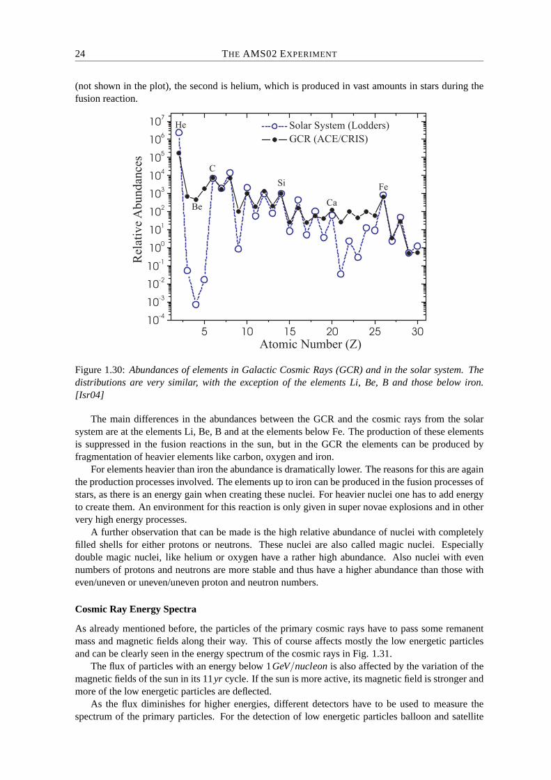
24 THE AMS02 EXPERIMENT
(not shown in the plot), the second is helium, which is produced in vast amounts in stars during thefusion reaction.
Rel
ativ
eA
bundan
ces
Atomic Number (Z)
Solar System (Lodders)
GCR (ACE/CRIS)
He
Be
C
Si
Ca
Fe
Figure 1.30: Abundances of elements in Galactic Cosmic Rays (GCR) and in the solar system. Thedistributions are very similar, with the exception of the elements Li, Be, B and those below iron.[Isr04]
The main differences in the abundances between the GCR and the cosmic rays from the solarsystem are at the elements Li, Be, B and at the elements below Fe. The production of these elementsis suppressed in the fusion reactions in the sun, but in the GCR the elements can be produced byfragmentation of heavier elements like carbon, oxygen and iron.
For elements heavier than iron the abundance is dramatically lower. The reasons for this are againthe production processes involved. The elements up to iron can be produced in the fusion processes ofstars, as there is an energy gain when creating these nuclei. For heavier nuclei one has to add energyto create them. An environment for this reaction is only given in super novae explosions and in othervery high energy processes.
A further observation that can be made is the high relative abundance of nuclei with completelyfilled shells for either protons or neutrons. These nuclei are also called magic nuclei. Especiallydouble magic nuclei, like helium or oxygen have a rather high abundance. Also nuclei with evennumbers of protons and neutrons are more stable and thus have a higher abundance than those witheven/uneven or uneven/uneven proton and neutron numbers.
Cosmic Ray Energy Spectra
As already mentioned before, the particles of the primary cosmic rays have to pass some remanentmass and magnetic fields along their way. This of course affects mostly the low energetic particlesand can be clearly seen in the energy spectrum of the cosmic rays in Fig. 1.31.
The flux of particles with an energy below 1GeV/nucleon is also affected by the variation of themagnetic fields of the sun in its 11yr cycle. If the sun is more active, its magnetic field is stronger andmore of the low energetic particles are deflected.
As the flux diminishes for higher energies, different detectors have to be used to measure thespectrum of the primary particles. For the detection of low energetic particles balloon and satellite
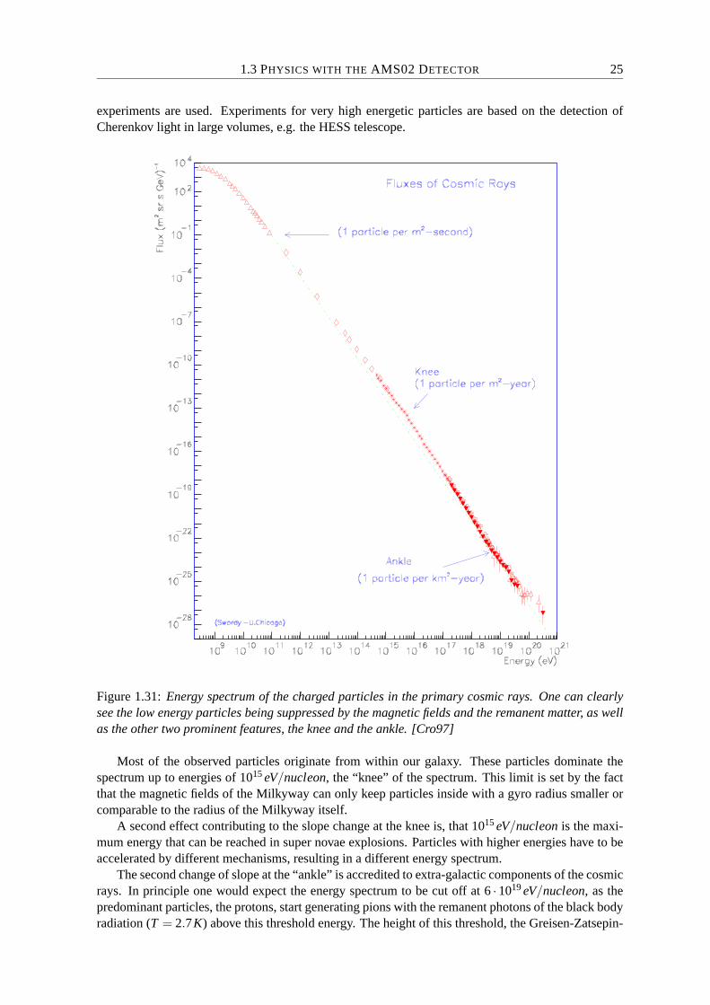
1.3 PHYSICS WITH THE AMS02 DETECTOR 25
experiments are used. Experiments for very high energetic particles are based on the detection ofCherenkov light in large volumes, e.g. the HESS telescope.
Figure 1.31: Energy spectrum of the charged particles in the primary cosmic rays. One can clearlysee the low energy particles being suppressed by the magnetic fields and the remanent matter, as wellas the other two prominent features, the knee and the ankle. [Cro97]
Most of the observed particles originate from within our galaxy. These particles dominate thespectrum up to energies of 1015 eV/nucleon, the “knee” of the spectrum. This limit is set by the factthat the magnetic fields of the Milkyway can only keep particles inside with a gyro radius smaller orcomparable to the radius of the Milkyway itself.
A second effect contributing to the slope change at the knee is, that 1015 eV/nucleon is the maxi-mum energy that can be reached in super novae explosions. Particles with higher energies have to beaccelerated by different mechanisms, resulting in a different energy spectrum.
The second change of slope at the “ankle” is accredited to extra-galactic components of the cosmicrays. In principle one would expect the energy spectrum to be cut off at 6 · 1019 eV/nucleon, as thepredominant particles, the protons, start generating pions with the remanent photons of the black bodyradiation (T = 2.7K) above this threshold energy. The height of this threshold, the Greisen-Zatsepin-

26 THE AMS02 EXPERIMENT
Kuzmin cut-off, can be calculated using the four vector balance of the proton and the photon.Nevertheless, some events have been observed with energies above 1020 eV/nucleon. The attenu-
ation length of particles with such energies is smaller than 10Mpc. For photons the attenuation lengthat such energies is even smaller (10kpc), as they generate electron positron pairs with the photons ofthe black body radiation. Also neutrinos can be discarded as candidates for these events, as they wouldhave a uniform distribution of events in the atmosphere (unlike the observed ones, that originated onlyfrom one layer of the atmosphere), due to their very low interaction probability.
Acceleration Mechanisms
How are the charged particles in the cosmic rays accelerated to such high energies? This is one ofthe questions in cosmology, that have not been finally answered up to now. There are many modelsdescribing mechanisms for various energy regimes, but none gives a complete picture. Some of themare introduced below.
• Cyclotron mechanisms: Particles with energies of up to 100GeV have been detected andtraced back to our sun. These energies can be achieved by accelerating the particles in localisedvariable magnetic fields on the sun’s surface. There are two models, both of them are based onthe solar spots.
– Single Solar Spots: Solar spots are one of the most prominent features of the surface ofthe sun. They can be recognised by their colour, as they are cooler than the surroundingsurface and thus darker. The missing energy is “converted” into magnetic fields. Thesefields can reach strengths of a few T , which can be shown measuring the Zeemann effect,and sizes of up to 107 m.
If a charged particle is moved around such an area with the diameter R with a variablemagnetic field once, it is accelerated by the induced voltage and thus gains the energy:
E = eU = −edΦdt
= −e
∫ −→B ·d−→A
dt= eπR2 dB
dt(1.1)
The main problem of this model is, that it requires an additional force that keeps theparticle on its track around the solar spot, not unlike in the accelerator rings at CERN orFermilab.
– Pairs of Solar Spots: In a lot of cases there is not a single solar spot, but a pair of themwith opposite magnetic fields. The solar spot in these pairs move towards each other andmerge later on.
The moving magnetic dipole induces an electric field, that is perpendicular to the magneticdipole and to the direction of the movement,
−→E = −→v ×−→
B .
With the typical values for the magnetic field and the velocity, the electrical field can reachstrengths of 10V/m. Even though this value is rather small, due to the very small frictionlosses in the chromosphere and the huge dimensions of the solar spots, the particles canbe accelerated to energies in the GeV range.
This mechanism is much more plausible as a model for the particle acceleration on stars,as it does not require additional forces, that keep the particle on a circular track around thesolar spot.
• Fermi mechanism: The processes involving collisions of the particle with galactic clouds arecalled Fermi mechanisms. The 1st order process involves particle clouds emitted from explo-ding stars, the 2nd order process so-called magnetic clouds. Both processes generate very highenergetic particles.

1.3 PHYSICS WITH THE AMS02 DETECTOR 27
– 1st order: If a star has completely burned its hydrogen, a gravitational collapse will start,as the radiation pressure maintaining the balance is missing. This collapse increases thetemperature inside the star until the helium burning starts. Once the helium is consumedthe collapse continues. This process goes on till the fusion processes end at the iron group,as further fusion processes would be endothermic.
At this moment, at the latest, the star collapses fully. During this, it emits parts of its massinto the stellar void, the rest forms a neutron star. The emitted mass acts as a shock frontto the mass in the interstellar space.
If the shock front moves at the velocity of u1, the gas behind it moves away from it withthe velocity u2, which corresponds to u1−u2 in the lab system. A particle with the speed vthat encounters the shock front coming towards it, is reflected there and gains the energy:
∆E =12
m(v+(u1 −u2))2 − 1
2mv2 (1.2)
If one takes into account the relativistic corrections and the different scattering angles andthe approximation that v ≈ c, one gets the expression, as the linear terms dominate:
∆EE
=43
u1 −u2
c(1.3)
Similar expressions can be obtained for particles reflected between two shock fronts.
In most cases the inner wave of the shock front will be moving with higher velocities (v2)while the outer wave (v1) will be already slowed down by interactions with the interstellarmatter.
If a particle is reflected between the inner and the outer wave of the shock front, it willgain the energy
∆E1 =12
m(v+ v2)2 − 1
2mv2 (1.4)
at the inner front and loose the energy
∆E2 =12
m(v− v1)2 − 1
2mv2 (1.5)
at the outer front. Still there is a net gain in energy of
∆E =12
(v2
1 + v22 +2v(v2 − v1)
) ≈ mv∆v (1.6)
As both of these processes are linear in the relative velocity, they are called 1st Fermi-Mechanisms. Taking into account the measured values for the velocities, energies of upto 100TeV can be achieved with this acceleration processes.
– 2nd order: For collisions with magnetic clouds, one has to look at the two possibilities forsuch a collision: (a) the cloud is moving anti-parallel with the velocity −→u to the particle(velocity −→v ) or (b) parallel to it.
In the case (a) the particle gains the energy
∆E1 =12
m(v+u)2 − 12
mv2 (1.7)
for (b) it loses the energy
∆E2 =12
m(v−u)2 − 12
mv2 (1.8)
in average there is a net gain of energy for the particle of
∆E = ∆E1 +∆E2 = mu2 (1.9)
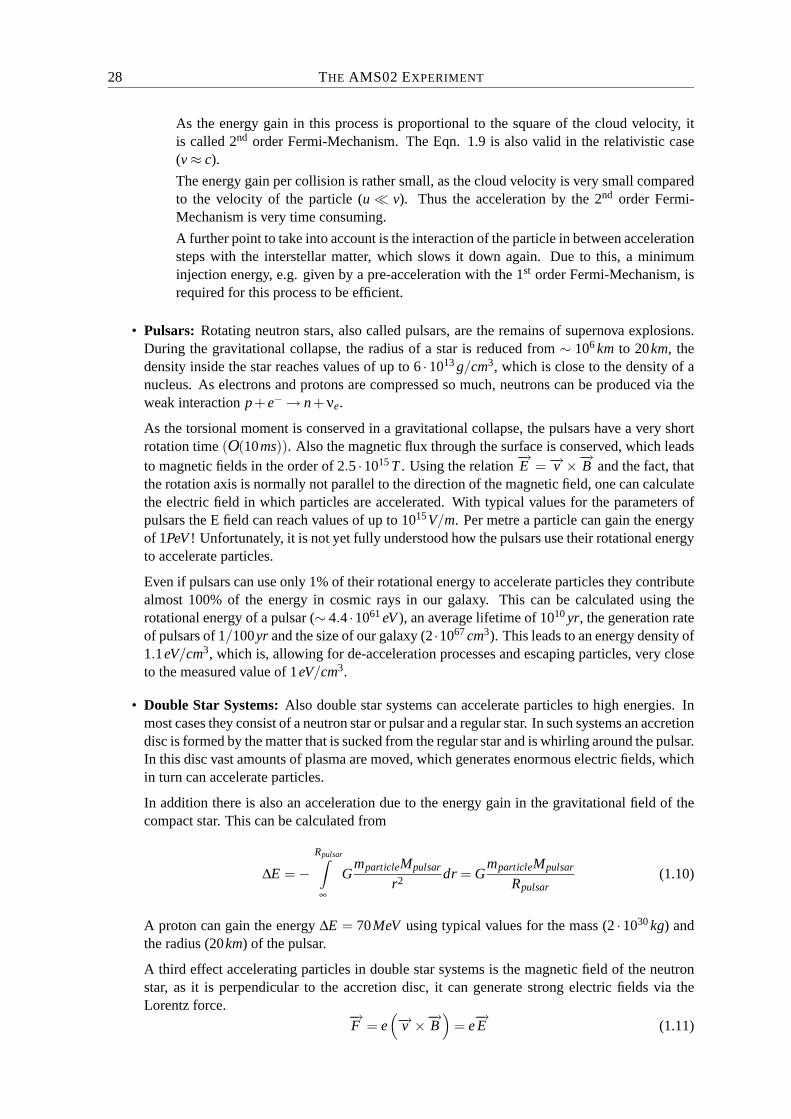
28 THE AMS02 EXPERIMENT
As the energy gain in this process is proportional to the square of the cloud velocity, itis called 2nd order Fermi-Mechanism. The Eqn. 1.9 is also valid in the relativistic case(v ≈ c).
The energy gain per collision is rather small, as the cloud velocity is very small comparedto the velocity of the particle (u v). Thus the acceleration by the 2nd order Fermi-Mechanism is very time consuming.
A further point to take into account is the interaction of the particle in between accelerationsteps with the interstellar matter, which slows it down again. Due to this, a minimuminjection energy, e.g. given by a pre-acceleration with the 1st order Fermi-Mechanism, isrequired for this process to be efficient.
• Pulsars: Rotating neutron stars, also called pulsars, are the remains of supernova explosions.During the gravitational collapse, the radius of a star is reduced from ∼ 106 km to 20km, thedensity inside the star reaches values of up to 6 ·1013 g/cm3, which is close to the density of anucleus. As electrons and protons are compressed so much, neutrons can be produced via theweak interaction p+ e− → n+νe.
As the torsional moment is conserved in a gravitational collapse, the pulsars have a very shortrotation time (O(10ms)). Also the magnetic flux through the surface is conserved, which leadsto magnetic fields in the order of 2.5 ·1015 T . Using the relation
−→E = −→v ×−→
B and the fact, thatthe rotation axis is normally not parallel to the direction of the magnetic field, one can calculatethe electric field in which particles are accelerated. With typical values for the parameters ofpulsars the E field can reach values of up to 1015V/m. Per metre a particle can gain the energyof 1PeV ! Unfortunately, it is not yet fully understood how the pulsars use their rotational energyto accelerate particles.
Even if pulsars can use only 1% of their rotational energy to accelerate particles they contributealmost 100% of the energy in cosmic rays in our galaxy. This can be calculated using therotational energy of a pulsar (∼ 4.4 ·1061 eV ), an average lifetime of 1010 yr, the generation rateof pulsars of 1/100yr and the size of our galaxy (2 ·1067 cm3). This leads to an energy density of1.1eV/cm3, which is, allowing for de-acceleration processes and escaping particles, very closeto the measured value of 1eV/cm3.
• Double Star Systems: Also double star systems can accelerate particles to high energies. Inmost cases they consist of a neutron star or pulsar and a regular star. In such systems an accretiondisc is formed by the matter that is sucked from the regular star and is whirling around the pulsar.In this disc vast amounts of plasma are moved, which generates enormous electric fields, whichin turn can accelerate particles.
In addition there is also an acceleration due to the energy gain in the gravitational field of thecompact star. This can be calculated from
∆E = −Rpulsar∫∞
GmparticleMpulsar
r2 dr = GmparticleMpulsar
Rpulsar(1.10)
A proton can gain the energy ∆E = 70MeV using typical values for the mass (2 · 1030 kg) andthe radius (20km) of the pulsar.
A third effect accelerating particles in double star systems is the magnetic field of the neutronstar, as it is perpendicular to the accretion disc, it can generate strong electric fields via theLorentz force. −→
F = e(−→v ×−→
B)
= e−→E (1.11)

1.3 PHYSICS WITH THE AMS02 DETECTOR 29
Form this, one can calculate the energy of a particle as
E =∫ −→
F ·d−→s = evB∆s (1.12)
using −→v ⊥−→B . For realistic values of v, B and ∆s, the energy of the particle can reach values of
3 ·1019 eV .
• Active Galaxy Nuclei: As a further source of high energetic particles also Active Galaxy Nuclei(AGN) are considered. Their acceleration mechanism is also based on the magnetic fields andthe particles moving in the accretion discs. As the characteristic values of the parameters inEqn. 1.12 are even higher than for double star systems, much higher energies can be achieved.Most of these particles are ejected from the system via the jets standing perpendicular on theaccretion discs.
In the current understanding, it is assumed, that the Fermi mechanisms are responsible for themain part of the cosmic ray spectrum (E < 1015 eV ). The higher energetic particles are believed tooriginate from pulsars, double star systems and AGNs.
For the acceleration in supernova shock waves one can calculate the energy spectrum of the par-ticles accelerated there. If the particle has the starting energy E0 and gains the energy εE in eachacceleration step it has the energy
En = E0(1+ ε)n (1.13)
after the nth step. Thus to reach the final energy of En the particle has to undergo n acceleration steps.
n =E/E0
ln(1+ ε)(1.14)
Taking into account the escape probability P after each step, one can calculate the number of particleswith an energy higher than E.
N(> E) ∼∞
∑m=n
(1−P)m =(1−P)m
P(1.15)
Using the Eqns. 1.15 and 1.14 one gets the integral energy spectrum
N(> E) ∼ 1P
(EE0
)−γ(1.16)
with the spectral index γ. Since the energy gain per step can be considered as very small compared tothe starting energy, one can express γ as
γ =ln(1+P)ln(1+ ε)
≈ Pε
(1.17)
From the measurement of the spectrum one gets for γ the value 1.7 for energies below 1015 eV andγ = 2 for energies above. This is in good agreement with the calculation.
1.3.3 Cosmic Rays - Anti-Matter
Dirac’s equation, E2 = m20c4 + p2c2, has two solutions, one for matter, one for anti-matter. Taking this
into account, one would expect from the models of the Big Bang an evenly balanced distribution ofmatter and anti-matter in the universe, as there is no known process favouring one or the other.
Any such process would have to be non-conserving for the baryon number. Additionally, thecharge parity (CP) would have to be violated to create a matter/anti-matter asymmetry. The CP vio-lation has been observed in the kaon decay in 1964 and is also understood from the theoretical view-point.
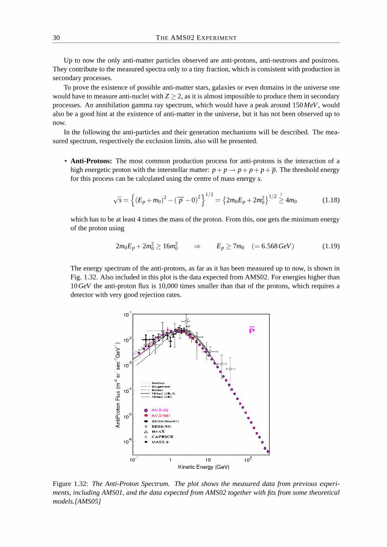
30 THE AMS02 EXPERIMENT
Up to now the only anti-matter particles observed are anti-protons, anti-neutrons and positrons.They contribute to the measured spectra only to a tiny fraction, which is consistent with production insecondary processes.
To prove the existence of possible anti-matter stars, galaxies or even domains in the universe onewould have to measure anti-nuclei with Z ≥ 2, as it is almost impossible to produce them in secondaryprocesses. An annihilation gamma ray spectrum, which would have a peak around 150MeV , wouldalso be a good hint at the existence of anti-matter in the universe, but it has not been observed up tonow.
In the following the anti-particles and their generation mechanisms will be described. The mea-sured spectrum, respectively the exclusion limits, also will be presented.
• Anti-Protons: The most common production process for anti-protons is the interaction of ahigh energetic proton with the interstellar matter: p+ p → p+ p+ p+ p. The threshold energyfor this process can be calculated using the centre of mass energy s.
√s =
(Ep +m0)
2 − (−→p −0)21/2
=
2m0Ep +2m20
1/2 !≥ 4m0 (1.18)
which has to be at least 4 times the mass of the proton. From this, one gets the minimum energyof the proton using
2m0Ep +2m20 ≥ 16m2
0 ⇒ Ep ≥ 7m0 (= 6.568GeV ) (1.19)
The energy spectrum of the anti-protons, as far as it has been measured up to now, is shown inFig. 1.32. Also included in this plot is the data expected from AMS02. For energies higher than10GeV the anti-proton flux is 10,000 times smaller than that of the protons, which requires adetector with very good rejection rates.
Figure 1.32: The Anti-Proton Spectrum. The plot shows the measured data from previous experi-ments, including AMS01, and the data expected from AMS02 together with fits from some theoreticalmodels.[AMS05]
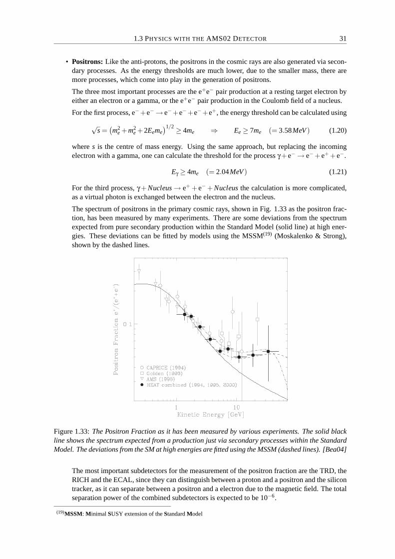
1.3 PHYSICS WITH THE AMS02 DETECTOR 31
• Positrons: Like the anti-protons, the positrons in the cosmic rays are also generated via secon-dary processes. As the energy thresholds are much lower, due to the smaller mass, there aremore processes, which come into play in the generation of positrons.
The three most important processes are the e+e− pair production at a resting target electron byeither an electron or a gamma, or the e+e− pair production in the Coulomb field of a nucleus.
For the first process, e−+e− → e−+e−+e−+e+, the energy threshold can be calculated using
√s =
(m2
e +m2e +2Eeme
)1/2 ≥ 4me ⇒ Ee ≥ 7me (= 3.58MeV ) (1.20)
where s is the centre of mass energy. Using the same approach, but replacing the incomingelectron with a gamma, one can calculate the threshold for the process γ+ e− → e− + e+ + e−.
Eγ ≥ 4me (= 2.04MeV ) (1.21)
For the third process, γ + Nucleus → e+ + e− + Nucleus the calculation is more complicated,as a virtual photon is exchanged between the electron and the nucleus.
The spectrum of positrons in the primary cosmic rays, shown in Fig. 1.33 as the positron frac-tion, has been measured by many experiments. There are some deviations from the spectrumexpected from pure secondary production within the Standard Model (solid line) at high ener-gies. These deviations can be fitted by models using the MSSM(19) (Moskalenko & Strong),shown by the dashed lines.
Figure 1.33: The Positron Fraction as it has been measured by various experiments. The solid blackline shows the spectrum expected from a production just via secondary processes within the StandardModel. The deviations from the SM at high energies are fitted using the MSSM (dashed lines). [Bea04]
The most important subdetectors for the measurement of the positron fraction are the TRD, theRICH and the ECAL, since they can distinguish between a proton and a positron and the silicontracker, as it can separate between a positron and a electron due to the magnetic field. The totalseparation power of the combined subdetectors is expected to be 10−6.
(19)MSSM: Minimal SUSY extension of the Standard Model
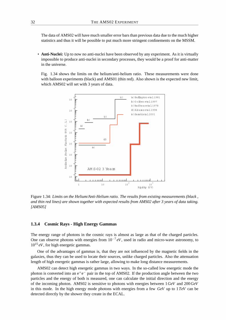
32 THE AMS02 EXPERIMENT
The data of AMS02 will have much smaller error bars than previous data due to the much higherstatistics and thus it will be possible to put much more stringent confinements on the MSSM.
• Anti-Nuclei: Up to now no anti-nuclei have been observed by any experiment. As it is virtuallyimpossible to produce anti-nuclei in secondary processes, they would be a proof for anti-matterin the universe.
Fig. 1.34 shows the limits on the helium/anti-helium ratio. These measurements were donewith balloon experiments (black) and AMS01 (thin red). Also shown is the expected new limit,which AMS02 will set with 3 years of data.
10-9
10-8
10-7
10-6
10-5
10-4
10-3
10-2
1 10 102
103
Antihelium/Helium Flux Ratio (95% C.L.)
Rigidity (G V)
(a) Buffington etal. 1981
(b) G olden etal. 1997
(c) Badhwar etal. 1978
(d) Alcaraz etal. 1998
(e) Sasaki etal. 2001
(a)
(b)(c)
(c)
(d)
(e)
AM S-02 3 Years
Figure 1.34: Limits on the Helium/Anti-Helium ratio. The results from existing measurements (black ,and thin red lines) are shown together with expected results from AMS02 after 3 years of data taking.[AMS05]
1.3.4 Cosmic Rays - High Energy Gammas
The energy range of photons in the cosmic rays is almost as large as that of the charged particles.One can observe photons with energies from 10−7 eV , used in radio and micro-wave astronomy, to1015 eV , for high energetic gammas.
One of the advantages of gammas is, that they are not influenced by the magnetic fields in thegalaxies, thus they can be used to locate their sources, unlike charged particles. Also the attenuationlength of high energetic gammas is rather large, allowing to make long distance measurements.
AMS02 can detect high energetic gammas in two ways. In the so-called low energetic mode thephoton is converted into an e+e− pair in the top of AMS02. If the production angle between the twoparticles and the energy of both is measured, one can calculate the initial direction and the energyof the incoming photon. AMS02 is sensitive to photons with energies between 1GeV and 200GeVin this mode. In the high energy mode photons with energies from a few GeV up to 1TeV can bedetected directly by the shower they create in the ECAL.

1.3 PHYSICS WITH THE AMS02 DETECTOR 33
Acceleration Mechanisms
Like charged particles, high energetic gammas also originate from supernovae, SNRs, fast rotatingobjects like pulsars, neutron stars or AGNs. In these objects gammas can be produced by the mecha-nisms listed below.
• Synchrotron Radiation: A charged particle emits radiation (= photons), if it is being acceler-ated. This radiation is called synchrotron radiation in the case of a magnetic field causing theaccelerating force. A detailed description of the synchrotron radiation can be found in [Jac98].
The synchrotron radiation in the cosmic magnetic fields is caused by ultra relativistic particles,which means electrons, as they have a much higher β than heavier particles.
The emitted power P for an electron of the energy E in the magnetic field B is
P ∝ E2 ·B2 (1.22)
It can be shown that the mean energy per photon is
〈ω〉 =8
15√
3ωc (1.23)
with ωc (in keV)≈ 2.22 ·E4/R, where E is the energy of the electron in GeV and R the bendingradius in m.
• Bremsstrahlung: The Bremsstrahlung is a phenomenon which is related to synchrotron radi-ation. Only in this case, the charged particle is not accelerated by a magnetic field, but by anelectric field. Again, the charged particle can emit a photon in this process. The probability Φfor the emission of a photon is given by
Φ ∝z2Z2E
m2 (1.24)
where z, m and E are charge, mass and energy of the incoming particle and Z is the charge ofthe target particle.
A more detailed description of the Bremsstrahlung can be found in [Jac98].
• Inverse Compton scattering: In the 1920s Compton discovered that photons scattered on freeelectrons can transfer a part of their energy to the electron. In the cosmos the inverse processproduces high energetic gammas: An electron with very high energy scatters on a photon andtransfers some of its energy to it. The photon, coming either from the black body radiation inthe universe or from the star light, is then “blue shifted”.
• π0 Decay: A further possibility for the production of high energetic gammas is the decay ofπ0s. The pions themselves are produced in the reaction
p+Nucleus → p′ +Nucleus′ +π+ +π− +π0 (1.25)
The π0 then decays into two gammas: π0 → γ+ γ. If the pion is at rest the gammas are emittedanti-parallel, both with half the rest mass of the pion (135MeV ) as energy. The emitted gammascan be boosted in the direction of the movement of the pion, but in most cases the energy of thepion is rather small, resulting in gamma energies around 70MeV .
• Matter - Anti-matter Annihilation: If an anti-matter particle collides with its matter counter-part it will annihilate. Due to the conservation of the impulse, the annihilation of electrons andpositrons produces two photons:
e+ + e− → γ+ γ (1.26)
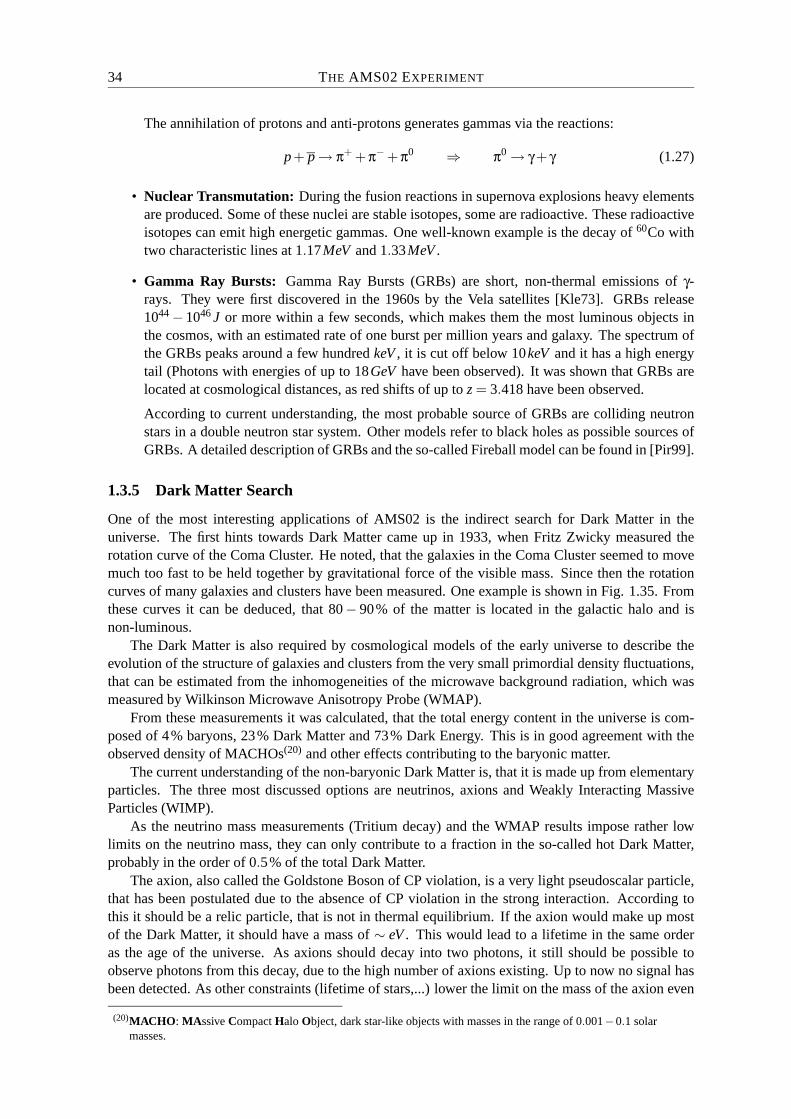
34 THE AMS02 EXPERIMENT
The annihilation of protons and anti-protons generates gammas via the reactions:
p+ p → π+ +π− +π0 ⇒ π0 → γ+ γ (1.27)
• Nuclear Transmutation: During the fusion reactions in supernova explosions heavy elementsare produced. Some of these nuclei are stable isotopes, some are radioactive. These radioactiveisotopes can emit high energetic gammas. One well-known example is the decay of 60Co withtwo characteristic lines at 1.17MeV and 1.33MeV .
• Gamma Ray Bursts: Gamma Ray Bursts (GRBs) are short, non-thermal emissions of γ-rays. They were first discovered in the 1960s by the Vela satellites [Kle73]. GRBs release1044 − 1046 J or more within a few seconds, which makes them the most luminous objects inthe cosmos, with an estimated rate of one burst per million years and galaxy. The spectrum ofthe GRBs peaks around a few hundred keV , it is cut off below 10keV and it has a high energytail (Photons with energies of up to 18GeV have been observed). It was shown that GRBs arelocated at cosmological distances, as red shifts of up to z = 3.418 have been observed.
According to current understanding, the most probable source of GRBs are colliding neutronstars in a double neutron star system. Other models refer to black holes as possible sources ofGRBs. A detailed description of GRBs and the so-called Fireball model can be found in [Pir99].
1.3.5 Dark Matter Search
One of the most interesting applications of AMS02 is the indirect search for Dark Matter in theuniverse. The first hints towards Dark Matter came up in 1933, when Fritz Zwicky measured therotation curve of the Coma Cluster. He noted, that the galaxies in the Coma Cluster seemed to movemuch too fast to be held together by gravitational force of the visible mass. Since then the rotationcurves of many galaxies and clusters have been measured. One example is shown in Fig. 1.35. Fromthese curves it can be deduced, that 80− 90% of the matter is located in the galactic halo and isnon-luminous.
The Dark Matter is also required by cosmological models of the early universe to describe theevolution of the structure of galaxies and clusters from the very small primordial density fluctuations,that can be estimated from the inhomogeneities of the microwave background radiation, which wasmeasured by Wilkinson Microwave Anisotropy Probe (WMAP).
From these measurements it was calculated, that the total energy content in the universe is com-posed of 4% baryons, 23% Dark Matter and 73% Dark Energy. This is in good agreement with theobserved density of MACHOs(20) and other effects contributing to the baryonic matter.
The current understanding of the non-baryonic Dark Matter is, that it is made up from elementaryparticles. The three most discussed options are neutrinos, axions and Weakly Interacting MassiveParticles (WIMP).
As the neutrino mass measurements (Tritium decay) and the WMAP results impose rather lowlimits on the neutrino mass, they can only contribute to a fraction in the so-called hot Dark Matter,probably in the order of 0.5% of the total Dark Matter.
The axion, also called the Goldstone Boson of CP violation, is a very light pseudoscalar particle,that has been postulated due to the absence of CP violation in the strong interaction. According tothis it should be a relic particle, that is not in thermal equilibrium. If the axion would make up mostof the Dark Matter, it should have a mass of ∼ eV . This would lead to a lifetime in the same orderas the age of the universe. As axions should decay into two photons, it still should be possible toobserve photons from this decay, due to the high number of axions existing. Up to now no signal hasbeen detected. As other constraints (lifetime of stars,...) lower the limit on the mass of the axion even
(20)MACHO: MAssive Compact Halo Object, dark star-like objects with masses in the range of 0.001−0.1 solarmasses.
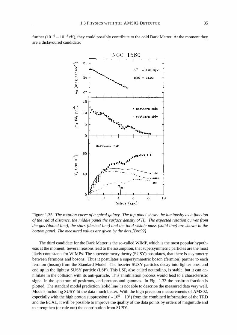
1.3 PHYSICS WITH THE AMS02 DETECTOR 35
further (10−6 −10−3 eV ), they could possibly contribute to the cold Dark Matter. At the moment theyare a disfavoured candidate.
Figure 1.35: The rotation curve of a spiral galaxy. The top panel shows the luminosity as a functionof the radial distance, the middle panel the surface density of HI. The expected rotation curves fromthe gas (dotted line), the stars (dashed line) and the total visible mass (solid line) are shown in thebottom panel. The measured values are given by the dots.[Bro92]
The third candidate for the Dark Matter is the so-called WIMP, which is the most popular hypoth-esis at the moment. Several reasons lead to the assumption, that supersymmetric particles are the mostlikely contestants for WIMPs. The supersymmetry theory (SUSY) postulates, that there is a symmetrybetween fermions and bosons. Thus it postulates a supersymmetric boson (fermion) partner to eachfermion (boson) from the Standard Model. The heavier SUSY particles decay into lighter ones andend up in the lightest SUSY particle (LSP). This LSP, also called neutralino, is stable, but it can an-nihilate in the collision with its anti-particle. This annihilation process would lead to a characteristicsignal in the spectrum of positrons, anti-protons and gammas. In Fig. 1.33 the positron fraction isplotted. The standard model prediction (solid line) is not able to describe the measured data very well.Models including SUSY fit the data much better. With the high precision measurements of AMS02,especially with the high proton suppression (∼ 105−106) from the combined information of the TRDand the ECAL, it will be possible to improve the quality of the data points by orders of magnitude andto strengthen (or rule out) the contribution from SUSY.
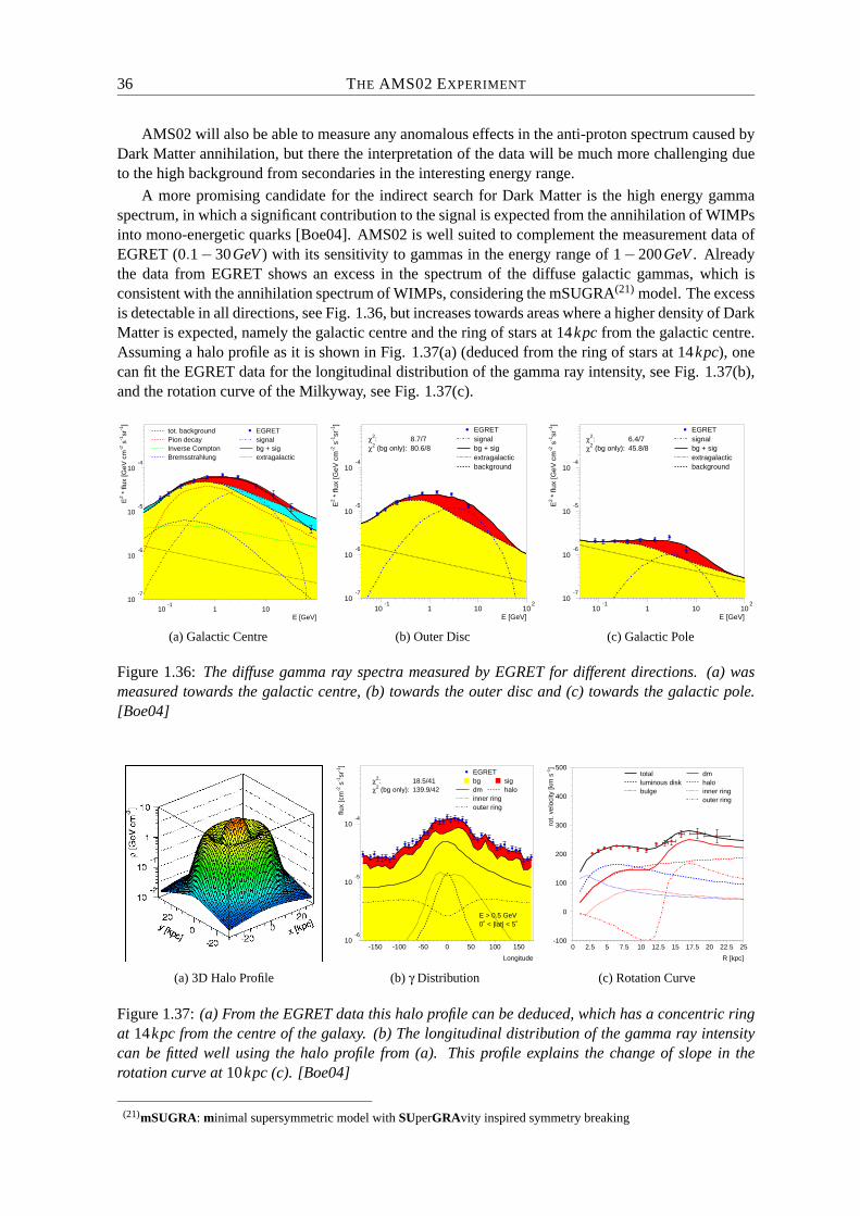
36 THE AMS02 EXPERIMENT
AMS02 will also be able to measure any anomalous effects in the anti-proton spectrum caused byDark Matter annihilation, but there the interpretation of the data will be much more challenging dueto the high background from secondaries in the interesting energy range.
A more promising candidate for the indirect search for Dark Matter is the high energy gammaspectrum, in which a significant contribution to the signal is expected from the annihilation of WIMPsinto mono-energetic quarks [Boe04]. AMS02 is well suited to complement the measurement data ofEGRET (0.1− 30GeV ) with its sensitivity to gammas in the energy range of 1− 200GeV . Alreadythe data from EGRET shows an excess in the spectrum of the diffuse galactic gammas, which isconsistent with the annihilation spectrum of WIMPs, considering the mSUGRA(21) model. The excessis detectable in all directions, see Fig. 1.36, but increases towards areas where a higher density of DarkMatter is expected, namely the galactic centre and the ring of stars at 14kpc from the galactic centre.Assuming a halo profile as it is shown in Fig. 1.37(a) (deduced from the ring of stars at 14kpc), onecan fit the EGRET data for the longitudinal distribution of the gamma ray intensity, see Fig. 1.37(b),and the rotation curve of the Milkyway, see Fig. 1.37(c).
10-7
10-6
10-5
10-4
10-1
1 10E [GeV]
E2 *
flux
[GeV
cm
-2 s
-1sr
-1]
EGRETsignalbg + sigextragalactic
tot. backgroundPion decayInverse ComptonBremsstrahlung
(a) Galactic Centre
10-7
10-6
10-5
10-4
10-1
1 10 102
E [GeV]
E2 *
flux
[GeV
cm
-2 s
-1sr
-1]
EGRETsignalbg + sigextragalacticbackground
χ2: 8.7/7χ2 (bg only): 80.6/8
(b) Outer Disc
10-7
10-6
10-5
10-4
10-1
1 10 102
E [GeV]
E2 *
flux
[GeV
cm
-2 s
-1sr
-1]
EGRETsignalbg + sigextragalacticbackground
χ2: 6.4/7χ2 (bg only): 45.8/8
(c) Galactic Pole
Figure 1.36: The diffuse gamma ray spectra measured by EGRET for different directions. (a) wasmeasured towards the galactic centre, (b) towards the outer disc and (c) towards the galactic pole.[Boe04]
(a) 3D Halo Profile
10-6
10-5
10-4
-150 -100 -50 0 50 100 150
Longitude
flux
[cm
-2 s
-1sr
-1]
EGRETbg sigdm haloinner ringouter ring
χ2: 18.5/41χ2 (bg only): 139.9/42
E > 0.5 GeV0˚ < |lat| < 5˚
(b) γ Distribution
-100
0
100
200
300
400
500
0 2.5 5 7.5 10 12.5 15 17.5 20 22.5 25
R [kpc]
rot.
velo
city
[km
s-1
]
totalluminous diskbulge
dmhaloinner ringouter ring
(c) Rotation Curve
Figure 1.37: (a) From the EGRET data this halo profile can be deduced, which has a concentric ringat 14kpc from the centre of the galaxy. (b) The longitudinal distribution of the gamma ray intensitycan be fitted well using the halo profile from (a). This profile explains the change of slope in therotation curve at 10kpc (c). [Boe04]
(21)mSUGRA: minimal supersymmetric model with SUperGRAvity inspired symmetry breaking
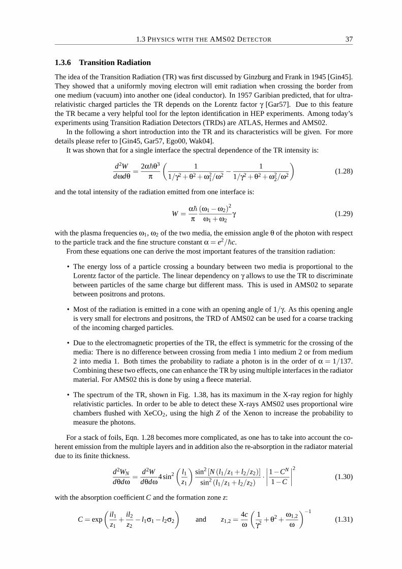
1.3 PHYSICS WITH THE AMS02 DETECTOR 37
1.3.6 Transition Radiation
The idea of the Transition Radiation (TR) was first discussed by Ginzburg and Frank in 1945 [Gin45].They showed that a uniformly moving electron will emit radiation when crossing the border fromone medium (vacuum) into another one (ideal conductor). In 1957 Garibian predicted, that for ultra-relativistic charged particles the TR depends on the Lorentz factor γ [Gar57]. Due to this featurethe TR became a very helpful tool for the lepton identification in HEP experiments. Among today’sexperiments using Transition Radiation Detectors (TRDs) are ATLAS, Hermes and AMS02.
In the following a short introduction into the TR and its characteristics will be given. For moredetails please refer to [Gin45, Gar57, Ego00, Wak04].
It was shown that for a single interface the spectral dependence of the TR intensity is:
d2Wdωdθ
=2αθ3
π
(1
1/γ2 +θ2 +ω21/ω2
− 1
1/γ2 +θ2 +ω22/ω2
)(1.28)
and the total intensity of the radiation emitted from one interface is:
W =α
π(ω1 −ω2)
2
ω1 +ω2γ (1.29)
with the plasma frequencies ω1, ω2 of the two media, the emission angle θ of the photon with respectto the particle track and the fine structure constant α = e2/c.
From these equations one can derive the most important features of the transition radiation:
• The energy loss of a particle crossing a boundary between two media is proportional to theLorentz factor of the particle. The linear dependency on γ allows to use the TR to discriminatebetween particles of the same charge but different mass. This is used in AMS02 to separatebetween positrons and protons.
• Most of the radiation is emitted in a cone with an opening angle of 1/γ. As this opening angleis very small for electrons and positrons, the TRD of AMS02 can be used for a coarse trackingof the incoming charged particles.
• Due to the electromagnetic properties of the TR, the effect is symmetric for the crossing of themedia: There is no difference between crossing from media 1 into medium 2 or from medium2 into media 1. Both times the probability to radiate a photon is in the order of α = 1/137.Combining these two effects, one can enhance the TR by using multiple interfaces in the radiatormaterial. For AMS02 this is done by using a fleece material.
• The spectrum of the TR, shown in Fig. 1.38, has its maximum in the X-ray region for highlyrelativistic particles. In order to be able to detect these X-rays AMS02 uses proportional wirechambers flushed with XeCO2, using the high Z of the Xenon to increase the probability tomeasure the photons.
For a stack of foils, Eqn. 1.28 becomes more complicated, as one has to take into account the co-herent emission from the multiple layers and in addition also the re-absorption in the radiator materialdue to its finite thickness.
d2WN
dθdω=
d2Wdθdω
4sin2(
l1z1
)sin2 [N (l1/z1 + l2/z2)]
sin2 (l1/z1 + l2/z2)·∣∣∣∣1−CN
1−C
∣∣∣∣2
(1.30)
with the absorption coefficient C and the formation zone z:
C = exp
(il1z1
+il2z2
− l1σ1 − l2σ2
)and z1,2 =
4cω
(1γ2 +θ2 +
ω1,2
ω
)−1
(1.31)
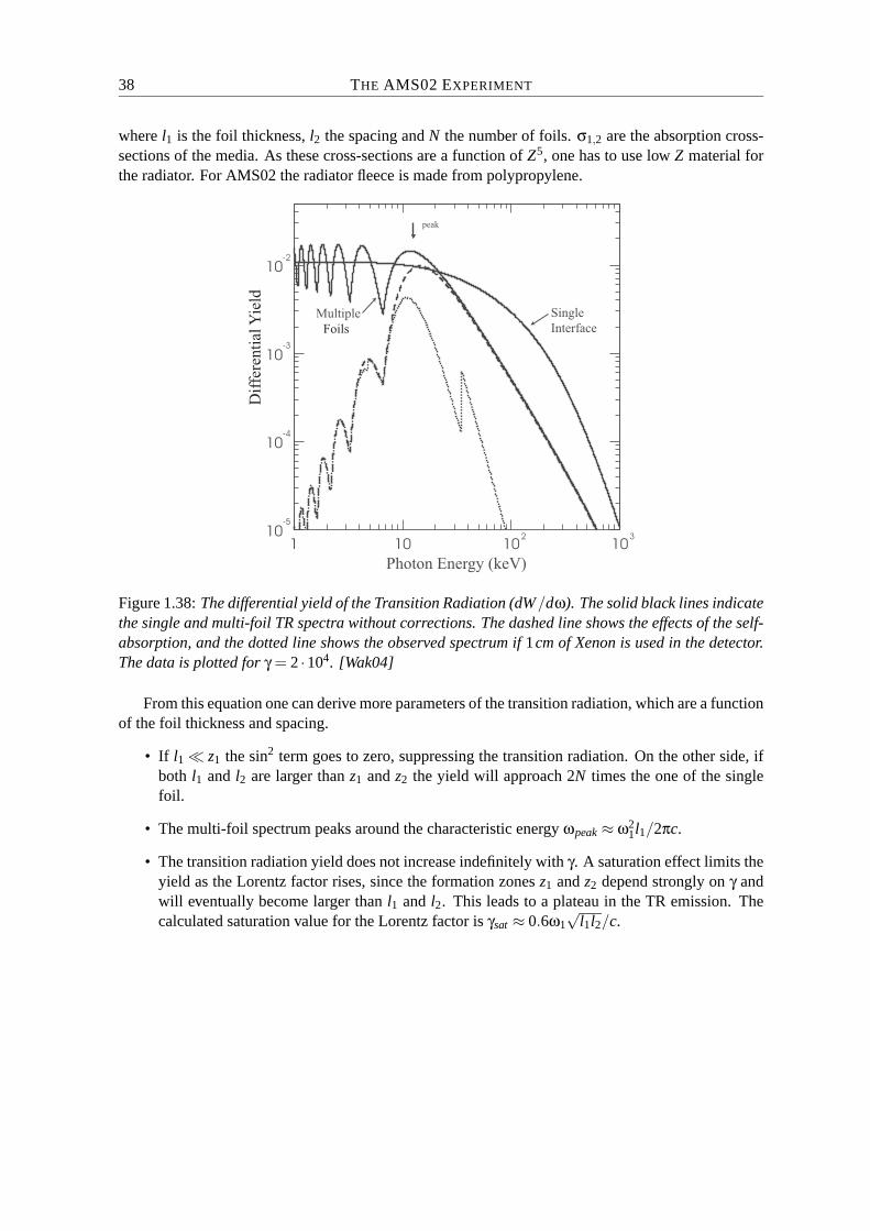
38 THE AMS02 EXPERIMENT
where l1 is the foil thickness, l2 the spacing and N the number of foils. σ1,2 are the absorption cross-sections of the media. As these cross-sections are a function of Z5, one has to use low Z material forthe radiator. For AMS02 the radiator fleece is made from polypropylene.
Photon Energy (keV)
1 10 102
10310
-5
10-4
10-3
10-2
peak
Single
Interface
Multiple
Foils
Dif
fere
nti
alY
ield
Figure 1.38: The differential yield of the Transition Radiation (dW/dω). The solid black lines indicatethe single and multi-foil TR spectra without corrections. The dashed line shows the effects of the self-absorption, and the dotted line shows the observed spectrum if 1cm of Xenon is used in the detector.The data is plotted for γ = 2 ·104. [Wak04]
From this equation one can derive more parameters of the transition radiation, which are a functionof the foil thickness and spacing.
• If l1 z1 the sin2 term goes to zero, suppressing the transition radiation. On the other side, ifboth l1 and l2 are larger than z1 and z2 the yield will approach 2N times the one of the singlefoil.
• The multi-foil spectrum peaks around the characteristic energy ωpeak ≈ ω21l1/2πc.
• The transition radiation yield does not increase indefinitely with γ. A saturation effect limits theyield as the Lorentz factor rises, since the formation zones z1 and z2 depend strongly on γ andwill eventually become larger than l1 and l2. This leads to a plateau in the TR emission. Thecalculated saturation value for the Lorentz factor is γsat ≈ 0.6ω1
√l1l2/c.

Chapter 2
Space-Grade Electronics for the AMS02Detector
The location of AMS02 on-board the ISS places stringent requirements on the detector and of coursealso on its electronics, shown in Fig. 2.1. This chapter will give an introduction into problems ofelectronics, when they are used in such hostile environments like space. A detailed overview of theelectronics of the AMS02 TRD will be given. For these electronics the responsibility lies with theInstitut fur Experimentelle Kernphysik at the University of Karlsruhe (TH). Following these remarks,the design and production process will be described as well as the testing and verification.
The description of the electronics and related issues will be quite detailed, as the system design,programming of the firmware of two slow-control cards and the testing of the electronics accordingto space-qualification rules was a major focus point of this thesis.
All abbreviations will be explained, as far as possible, on their first occurrence. For a completelist of the abbreviations used in this thesis please refer to the glossary on page 203.
(a) Wake Radiator (b) Ram Radiator
Figure 2.1: The wake (a) and ram (b) radiators of the AMS02 electronics. (wake and ram refer to theISS direction of travel) [AMS05]
39

40 SPACE-GRADE ELECTRONICS FOR THE AMS02 DETECTOR
2.1 Overall system design
With the experience of six decades of spacecraft engineering and operation, NASA has set up a systemto ensure the safety of the involved astronauts and to maximise the chances for a successful mission.
This system consists of many different parts, e.g. there are large databases containing informationon components that can be used for spacecrafts, but there are also review boards looking into theproject along its way at various critical stages to make sure that all NASA regulations are fulfilled.
For the electronics production AMS02 relies heavily on the existing know-how of NASA andspace technology companies. But in some areas AMS02 is also using new components, that were notused before for space applications. Each of these new parts was thoroughly tested by the collaborationbefore being allowed to be employed in the design.
As it is extremely difficult and dangerous to do maintenance on any spacecraft while it is on orbit,the design of such a spacecraft has to be done thoroughly and proven reliable before launch. Someof the tests involved in the verification of the design will be described in detail in section 2.5, as theyalso apply to the electronics of AMS02.
For a system such as AMS02, where the costs of training astronauts for maintenance would bevery high due to the immense complexity of the detector, this option is only chosen for vital systemslike the life support equipment. Due to this consideration, the AMS02 experiment was designed as azero maintenance system. With the exception of the ACOP(1), there will be no astronaut interventiononce AMS02 is mounted on its designated position on the S3 truss.
So the key point in the design of AMS02 is to protect all components where necessary and touse redundancy for all safety and mission success critical items. A good example for this is the mainDAQ computer of AMS02. It is fourfold redundant and each of the four computers is protected againstover-current, over-voltage and over-temperature.
2.2 AMS02 Electronics
In this section an overview of the electronics of the AMS02 experiment will be given. First thearchitecture of the DAQ chain will be discussed, followed by a description of the slow-control andmonitoring system.
The general overview of the electronics of the AMS02 experiment is shown in Fig. 2.2 togetherwith a scheme of the interfaces of AMS02 to the International Space Station.
For both the data and the slow control chain AMS02 uses tree-like architectures with a clear masterand slave structure. Schematic drawings of both trees are shown in Fig. 2.3 and Fig. 2.4.
(1)ACOP: AMS Crew Operations Post. The ACOP is a computer inside the ISS, which stores all data comingfrom the experiments and acts as a back-up slow-control and monitoring station.
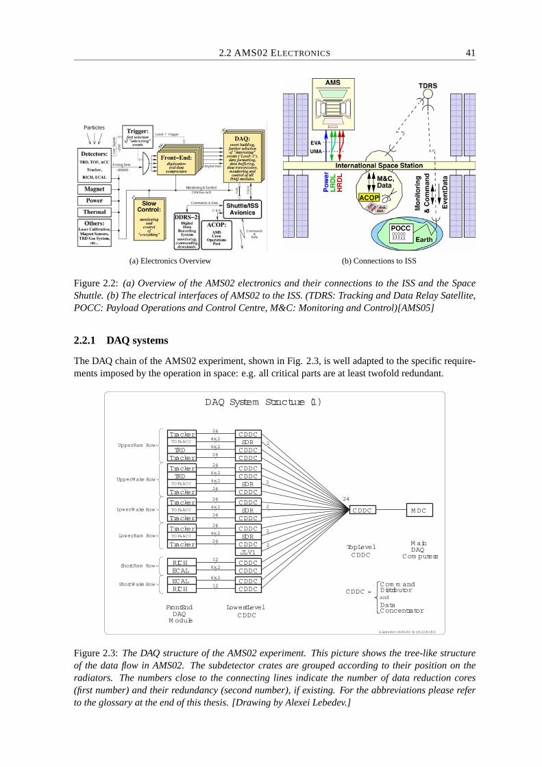
2.2 AMS02 ELECTRONICS 41
(a) Electronics Overview (b) Connections to ISS
Figure 2.2: (a) Overview of the AMS02 electronics and their connections to the ISS and the SpaceShuttle. (b) The electrical interfaces of AMS02 to the ISS. (TDRS: Tracking and Data Relay Satellite,POCC: Payload Operations and Control Centre, M&C: Monitoring and Control)[AMS05]
2.2.1 DAQ systems
The DAQ chain of the AMS02 experiment, shown in Fig. 2.3, is well adapted to the specific require-ments imposed by the operation in space: e.g. all critical parts are at least twofold redundant.
TopLevelM ainDAQ
Com puters
Com m andDistributorand
DataConcentrator
CDDC =
FrontEndDAQM odule
LowestLevelCDDC
CDDC
Tracker
TRDTracker
Tracker
Tracker
Tracker
Tracker
Tracker
TOF&ACC
TO F&ACC
TRDTOF&ACC
TO F&ACC
CDDC
CDDC
CDDCCDDC
CDDC
CDDC
Tracker
CDDCCDDC
M DC
CDDC
12
6x 2ECALRICH
242
JLV1CDDC
2
2
2
2
4x 2
6x 2
A.Lebedev 28/04/00 (m od.22/03/02)
DAQ System Structure (1)
24
6x 2
12
SDR
CDDC
SDR
CDDC
SDR
CDDCSDR
ECAL
4x 2
RICHCDDCCDDC
24
6x 2
24
24
24
24
24
24
4x 2
4x 2
Upper Ram Row
Upper Wake Row
Short Wake Row
Short Ram Row
Lower Ram Row
Lower W ake Row
Figure 2.3: The DAQ structure of the AMS02 experiment. This picture shows the tree-like structureof the data flow in AMS02. The subdetector crates are grouped according to their position on theradiators. The numbers close to the connecting lines indicate the number of data reduction cores(first number) and their redundancy (second number), if existing. For the abbreviations please referto the glossary at the end of this thesis. [Drawing by Alexei Lebedev.]
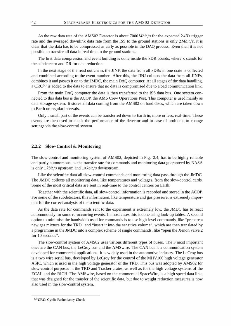
42 SPACE-GRADE ELECTRONICS FOR THE AMS02 DETECTOR
As the raw data rate of the AMS02 Detector is about 7000Mbit/s for the expected 2kHz triggerrate and the averaged downlink data rate from the ISS to the ground stations is only 2Mbit/s, it isclear that the data has to be compressed as early as possible in the DAQ process. Even then it is notpossible to transfer all data in real time to the ground stations.
The first data compression and event building is done inside the xDR boards, where x stands forthe subdetector and DR for data reduction.
In the next stage of the read out chain, the JINF, the data from all xDRs in one crate is collectedand combined according to the event number. After this, the JINJ collects the data from all JINFs,combines it and passes it on to the JMDC, the main DAQ computer. At all stages of the data handling,a CRC(2) is added to the data to ensure that no data is compromised due to a bad communication link.
From the main DAQ computer the data is then transferred to the ISS data bus. One system con-nected to this data bus is the ACOP, the AMS Crew Operations Post. This computer is used mainly asdata storage system. It stores all data coming from the AMS02 on hard discs, which are taken downto Earth on regular intervals.
Only a small part of the events can be transferred down to Earth in, more or less, real-time. Theseevents are then used to check the performance of the detector and in case of problems to changesettings via the slow-control system.
2.2.2 Slow-Control & Monitoring
The slow-control and monitoring system of AMS02, depicted in Fig. 2.4, has to be highly reliableand partly autonomous, as the transfer rate for commands and monitoring data guaranteed by NASAis only 1kbit/s upstream and 10kbit/s downstream.
Like the scientific data all slow-control commands and monitoring data pass through the JMDC.The JMDC collects all monitoring data, like temperatures and voltages, from the slow-control cards.Some of the most critical data are sent in real-time to the control centres on Earth.
Together with the scientific data, all slow-control information is recorded and stored in the ACOP.For some of the subdetectors, this information, like temperature and gas pressure, is extremely impor-tant for the correct analysis of the scientific data.
As the data rate for commands sent to the experiment is extremely low, the JMDC has to reactautonomously for some re-occurring events. In most cases this is done using look-up tables. A secondoption to minimise the bandwidth used for commands is to use high-level commands, like “prepare anew gas mixture for the TRD” and “insert it into the sensitive volume”, which are then translated bya programme in the JMDC into a complex scheme of single commands, like “open the Xenon valve 2for 10 seconds”.
The slow-control system of AMS02 uses various different types of buses. The 3 most importantones are the CAN bus, the LeCroy bus and the AMSwire. The CAN bus is a communication systemdeveloped for commercial applications. It is widely used in the automotive industry. The LeCroy busis a two wire serial bus, developed by LeCroy for the control of the MHV100 high voltage generatorASIC, which is used in the high voltage generator of the TRD. This bus was adopted by AMS02 forslow-control purposes in the TRD and Tracker crates, as well as for the high voltage systems of theECAL and the RICH. The AMSwire, based on the commercial SpaceWire, is a high speed data link,that was designed for the transfer of the scientific data, but due to weight reduction measures is nowalso used in the slow-control system.
(2)CRC: Cyclic Redundancy Check
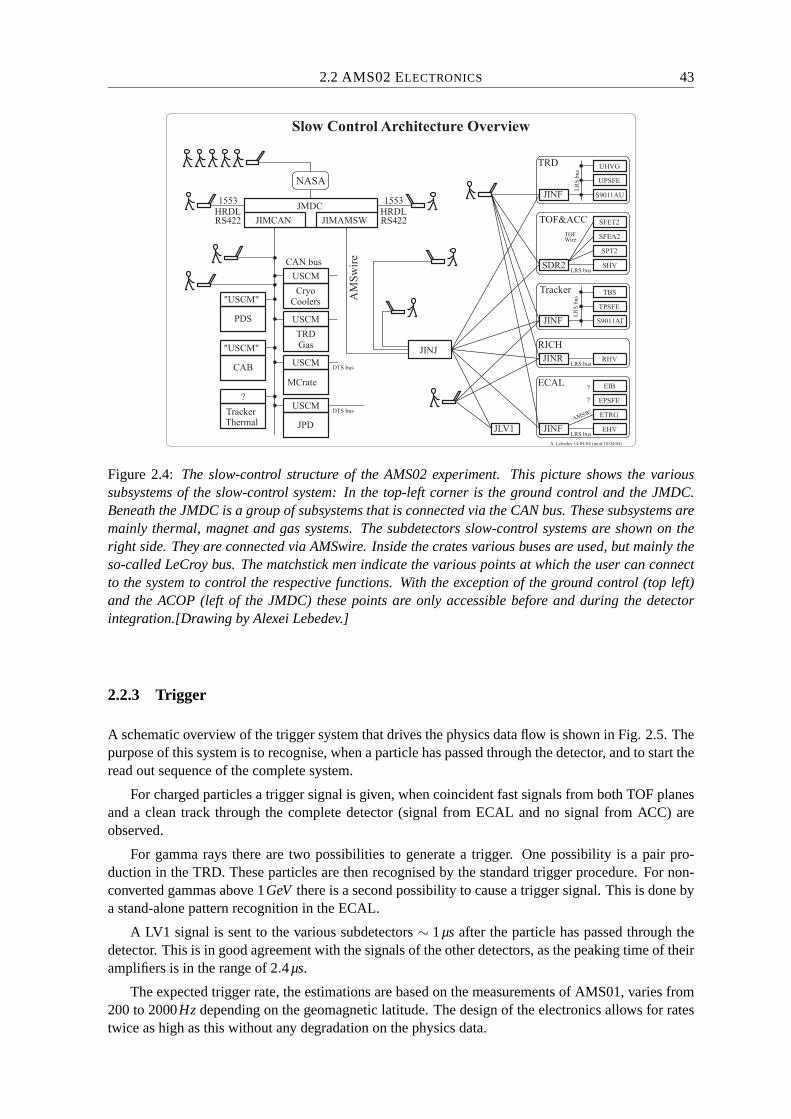
2.2 AMS02 ELECTRONICS 43
A. Lebedev 14/04/04 (mod.18/04/04)
JINF
TRD
Tracker
EIB
EPSFE
ETRG
S9011AU
JINF
UHVG
EHV
UPSFE
JINF
ECAL
JLV1
JINJ
"USCM"
PDS
SPT2
USCM
CoolersCryo
SFEA2
USCM
GasTRD
SFET2
USCM
MCrate
SHVSDR2
USCM
JPD
RICH
ThermalTracker
?
RHVJINR"USCM"
CAB
JIMCAN JIMAMSW
JMDC
NASA
S9011AT
TPSFE
TBS
LR
Sbus
AMSW
?
TOFWire
LRS bus
?
LRS bus
DTS bus
LR
Sbus
LRS bus
1553
DTS bus
CAN bus
HRDLRS422
1553HRDLRS422
Slow Control Architecture Overview
AM
Sw
ire
TOF&ACC
Figure 2.4: The slow-control structure of the AMS02 experiment. This picture shows the varioussubsystems of the slow-control system: In the top-left corner is the ground control and the JMDC.Beneath the JMDC is a group of subsystems that is connected via the CAN bus. These subsystems aremainly thermal, magnet and gas systems. The subdetectors slow-control systems are shown on theright side. They are connected via AMSwire. Inside the crates various buses are used, but mainly theso-called LeCroy bus. The matchstick men indicate the various points at which the user can connectto the system to control the respective functions. With the exception of the ground control (top left)and the ACOP (left of the JMDC) these points are only accessible before and during the detectorintegration.[Drawing by Alexei Lebedev.]
2.2.3 Trigger
A schematic overview of the trigger system that drives the physics data flow is shown in Fig. 2.5. Thepurpose of this system is to recognise, when a particle has passed through the detector, and to start theread out sequence of the complete system.
For charged particles a trigger signal is given, when coincident fast signals from both TOF planesand a clean track through the complete detector (signal from ECAL and no signal from ACC) areobserved.
For gamma rays there are two possibilities to generate a trigger. One possibility is a pair pro-duction in the TRD. These particles are then recognised by the standard trigger procedure. For non-converted gammas above 1GeV there is a second possibility to cause a trigger signal. This is done bya stand-alone pattern recognition in the ECAL.
A LV1 signal is sent to the various subdetectors ∼ 1µs after the particle has passed through thedetector. This is in good agreement with the signals of the other detectors, as the peaking time of theiramplifiers is in the range of 2.4µs.
The expected trigger rate, the estimations are based on the measurements of AMS01, varies from200 to 2000Hz depending on the geomagnetic latitude. The design of the electronics allows for ratestwice as high as this without any degradation on the physics data.
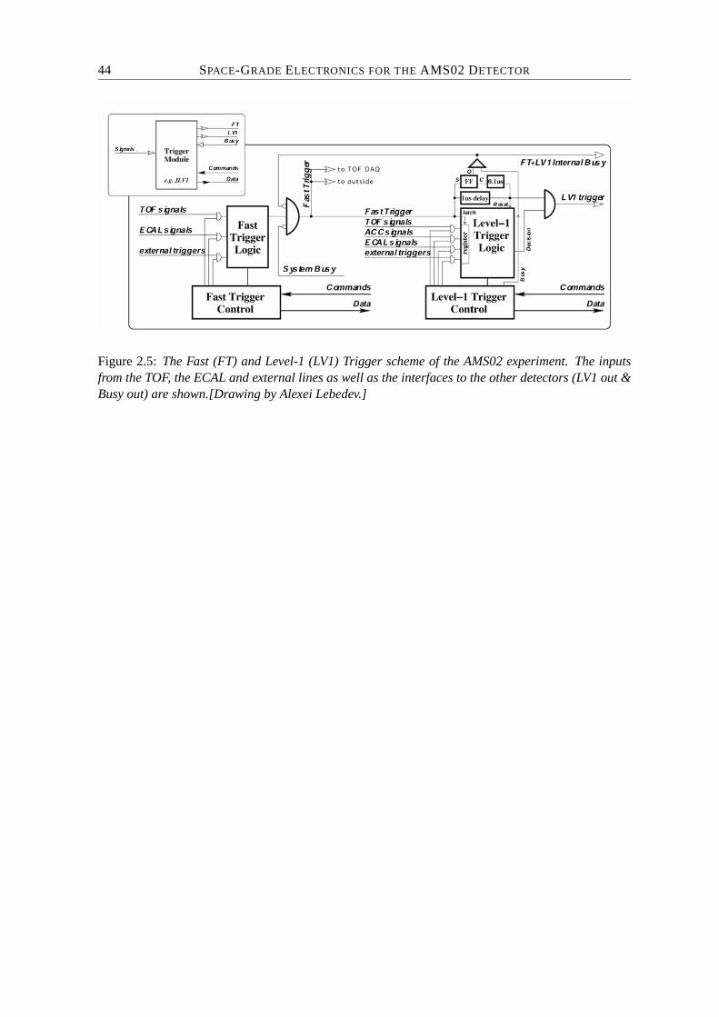
44 SPACE-GRADE ELECTRONICS FOR THE AMS02 DETECTOR
Figure 2.5: The Fast (FT) and Level-1 (LV1) Trigger scheme of the AMS02 experiment. The inputsfrom the TOF, the ECAL and external lines as well as the interfaces to the other detectors (LV1 out &Busy out) are shown.[Drawing by Alexei Lebedev.]
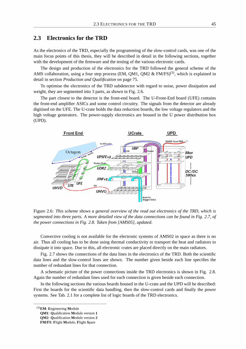
2.3 ELECTRONICS FOR THE TRD 45
2.3 Electronics for the TRD
As the electronics of the TRD, especially the programming of the slow-control cards, was one of themain focus points of this thesis, they will be described in detail in the following sections, togetherwith the development of the firmware and the testing of the various electronic cards.
The design and production of the electronics for the TRD followed the general scheme of theAMS collaboration, using a four step process (EM, QM1, QM2 & FM/FS)(3), which is explained indetail in section Production and Qualification on page 75.
To optimise the electronics of the TRD subdetector with regard to noise, power dissipation andweight, they are segmented into 3 parts, as shown in Fig. 2.6.
The part closest to the detector is the front-end board. The U-Front-End board (UFE) containsthe front-end amplifier ASICs and some control circuitry. The signals from the detector are alreadydigitised on the UFE. The U-crate holds the data reduction boards, the low voltage regulators and thehigh voltage generators. The power-supply electronics are housed in the U power distribution box(UPD).
Figure 2.6: This scheme shows a general overview of the read out electronics of the TRD, which issegmented into three parts. A more detailed view of the data connections can be found in Fig. 2.7, ofthe power connections in Fig. 2.8. Taken from [AMS05], updated.
Convective cooling is not available for the electronic systems of AMS02 in space as there is noair. Thus all cooling has to be done using thermal conductivity to transport the heat and radiators todissipate it into space. Due to this, all electronic crates are placed directly on the main radiators.
Fig. 2.7 shows the connections of the data lines in the electronics of the TRD. Both the scientificdata lines and the slow-control lines are shown. The number given beside each line specifies thenumber of redundant lines for that connection.
A schematic picture of the power connections inside the TRD electronics is shown in Fig. 2.8.Again the number of redundant lines used for each connection is given beside each connection.
In the following sections the various boards housed in the U-crate and the UPD will be described:First the boards for the scientific data handling, then the slow-control cards and finally the powersystems. See Tab. 2.1 for a complete list of logic boards of the TRD electronics.
(3)EM: Engineering ModuleQM1: Qualification Module version 1QM2: Qualification Module version 2FM/FS: Flight Module, Flight Spare
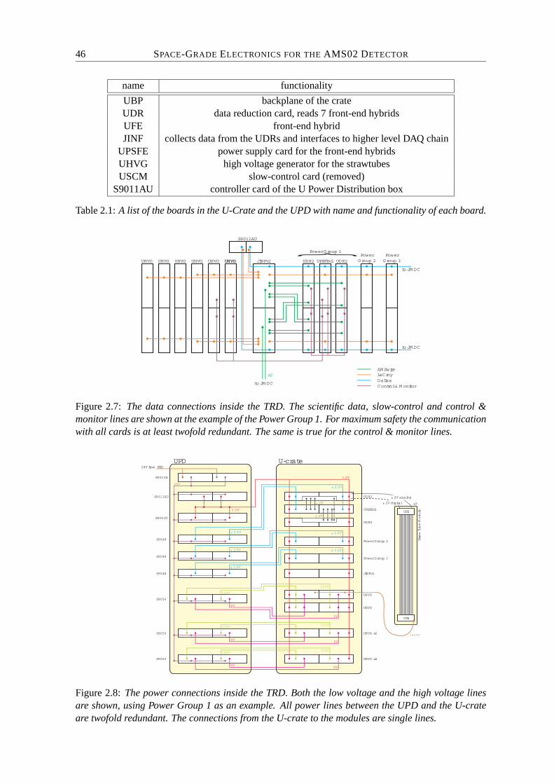
46 SPACE-GRADE ELECTRONICS FOR THE AMS02 DETECTOR
name functionality
UBP backplane of the crateUDR data reduction card, reads 7 front-end hybridsUFE front-end hybridJINF collects data from the UDRs and interfaces to higher level DAQ chain
UPSFE power supply card for the front-end hybridsUHVG high voltage generator for the strawtubesUSCM slow-control card (removed)
S9011AU controller card of the U Power Distribution box
Table 2.1: A list of the boards in the U-Crate and the UPD with name and functionality of each board.
JINFv2 UDR2 UDR2UPSFEv2UHVGUHVGUHVGUHVGUHVGUHVG UHVG
S9011AU
x2
to JM DC
to JM DC
to JM DC
PowerG roup 2
PowerG roup 3
AM SwireLeCroyDallasControl & M onitor
Power G roup 1
Figure 2.7: The data connections inside the TRD. The scientific data, slow-control and control &monitor lines are shown at the example of the Power Group 1. For maximum safety the communicationwith all cards is at least twofold redundant. The same is true for the control & monitor lines.
28V from PBD
UPD U-crate
S9011B
S9011AU
S9053U
S9048
S9048
S9048
S9056
S9056
S9056
UHVG
UDR2
UPSFEv2
UDR2
Power G roup 2
Power G roup 3
JINFv2
UHVG
UHVG x2
UHVG x2
UTE
UFE
x7
1600V
3.3V
± 2.5V
± 2.5V
± 2.5V
± 2V
± 2V
120V
120V
120V
5V
5V
5V
3.3V
± 2.5V
± 2.5V
± 2.5V
120V
120V
120V
5V
5V
5V
28V
± 2V digital
Straw Tube Module
± 2V analog
Figure 2.8: The power connections inside the TRD. Both the low voltage and the high voltage linesare shown, using Power Group 1 as an example. All power lines between the UPD and the U-crateare twofold redundant. The connections from the U-crate to the modules are single lines.
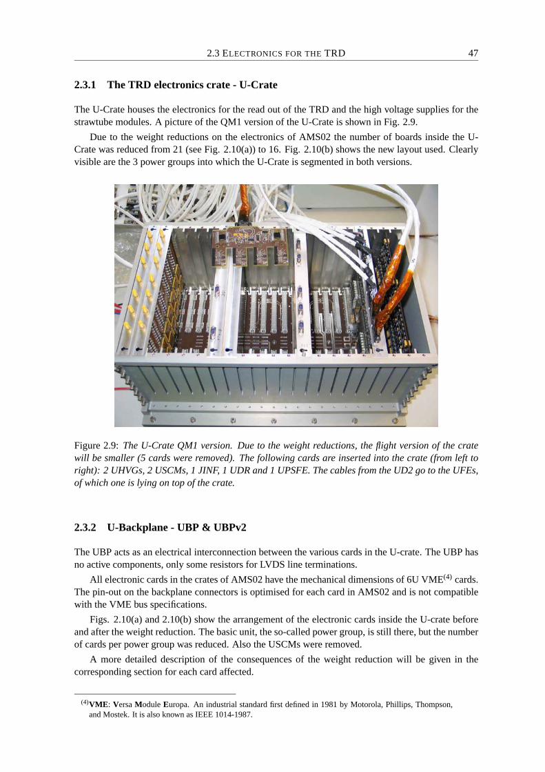
2.3 ELECTRONICS FOR THE TRD 47
2.3.1 The TRD electronics crate - U-Crate
The U-Crate houses the electronics for the read out of the TRD and the high voltage supplies for thestrawtube modules. A picture of the QM1 version of the U-Crate is shown in Fig. 2.9.
Due to the weight reductions on the electronics of AMS02 the number of boards inside the U-Crate was reduced from 21 (see Fig. 2.10(a)) to 16. Fig. 2.10(b) shows the new layout used. Clearlyvisible are the 3 power groups into which the U-Crate is segmented in both versions.
Figure 2.9: The U-Crate QM1 version. Due to the weight reductions, the flight version of the cratewill be smaller (5 cards were removed). The following cards are inserted into the crate (from left toright): 2 UHVGs, 2 USCMs, 1 JINF, 1 UDR and 1 UPSFE. The cables from the UD2 go to the UFEs,of which one is lying on top of the crate.
2.3.2 U-Backplane - UBP & UBPv2
The UBP acts as an electrical interconnection between the various cards in the U-crate. The UBP hasno active components, only some resistors for LVDS line terminations.
All electronic cards in the crates of AMS02 have the mechanical dimensions of 6U VME(4) cards.The pin-out on the backplane connectors is optimised for each card in AMS02 and is not compatiblewith the VME bus specifications.
Figs. 2.10(a) and 2.10(b) show the arrangement of the electronic cards inside the U-crate beforeand after the weight reduction. The basic unit, the so-called power group, is still there, but the numberof cards per power group was reduced. Also the USCMs were removed.
A more detailed description of the consequences of the weight reduction will be given in thecorresponding section for each card affected.
(4)VME: Versa Module Europa. An industrial standard first defined in 1981 by Motorola, Phillips, Thompson,and Mostek. It is also known as IEEE 1014-1987.
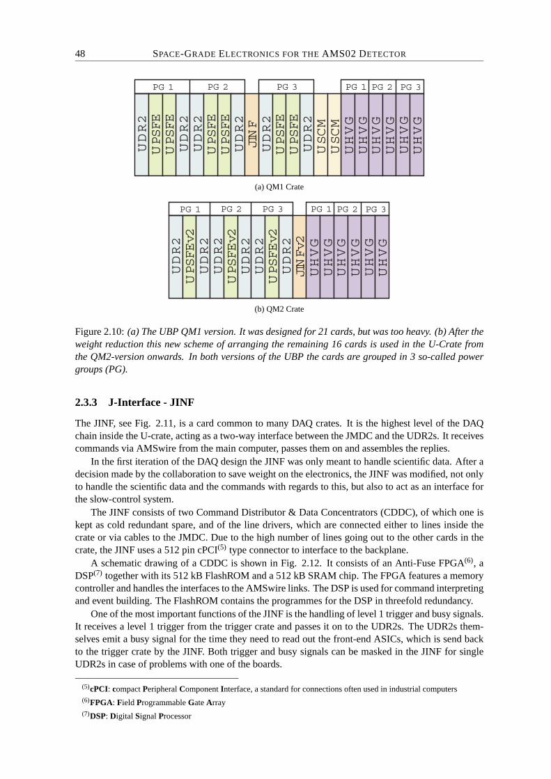
48 SPACE-GRADE ELECTRONICS FOR THE AMS02 DETECTOR
UDR2
UDR2
UDR2
UDR2
UDR2
UPSFE
UPSFE
UPSFE
JINF
UHVG
UHVG
UHVG
UHVG
UHVG
UHVG
PG 1 PG 2 PG 3 PG 1 PG 2 PG 3
UDR2
UPSFE
UPSFE
UPSFE
USCM
USCM
(a) QM1 CrateUDR2
UDR2
UDR2
UDR2
UDR2
UDR2
UPSFEv2
UPSFEv2
UPSFEv2
JINFv2
UHVG
UHVG
UHVG
UHVG
UHVG
UHVG
PG 1 PG 2 PG 3 PG 1 PG 2 PG 3
(b) QM2 Crate
Figure 2.10: (a) The UBP QM1 version. It was designed for 21 cards, but was too heavy. (b) After theweight reduction this new scheme of arranging the remaining 16 cards is used in the U-Crate fromthe QM2-version onwards. In both versions of the UBP the cards are grouped in 3 so-called powergroups (PG).
2.3.3 J-Interface - JINF
The JINF, see Fig. 2.11, is a card common to many DAQ crates. It is the highest level of the DAQchain inside the U-crate, acting as a two-way interface between the JMDC and the UDR2s. It receivescommands via AMSwire from the main computer, passes them on and assembles the replies.
In the first iteration of the DAQ design the JINF was only meant to handle scientific data. After adecision made by the collaboration to save weight on the electronics, the JINF was modified, not onlyto handle the scientific data and the commands with regards to this, but also to act as an interface forthe slow-control system.
The JINF consists of two Command Distributor & Data Concentrators (CDDC), of which one iskept as cold redundant spare, and of the line drivers, which are connected either to lines inside thecrate or via cables to the JMDC. Due to the high number of lines going out to the other cards in thecrate, the JINF uses a 512 pin cPCI(5) type connector to interface to the backplane.
A schematic drawing of a CDDC is shown in Fig. 2.12. It consists of an Anti-Fuse FPGA(6), aDSP(7) together with its 512 kB FlashROM and a 512 kB SRAM chip. The FPGA features a memorycontroller and handles the interfaces to the AMSwire links. The DSP is used for command interpretingand event building. The FlashROM contains the programmes for the DSP in threefold redundancy.
One of the most important functions of the JINF is the handling of level 1 trigger and busy signals.It receives a level 1 trigger from the trigger crate and passes it on to the UDR2s. The UDR2s them-selves emit a busy signal for the time they need to read out the front-end ASICs, which is send backto the trigger crate by the JINF. Both trigger and busy signals can be masked in the JINF for singleUDR2s in case of problems with one of the boards.
(5)cPCI: compact Peripheral Component Interface, a standard for connections often used in industrial computers(6)FPGA: Field Programmable Gate Array(7)DSP: Digital Signal Processor
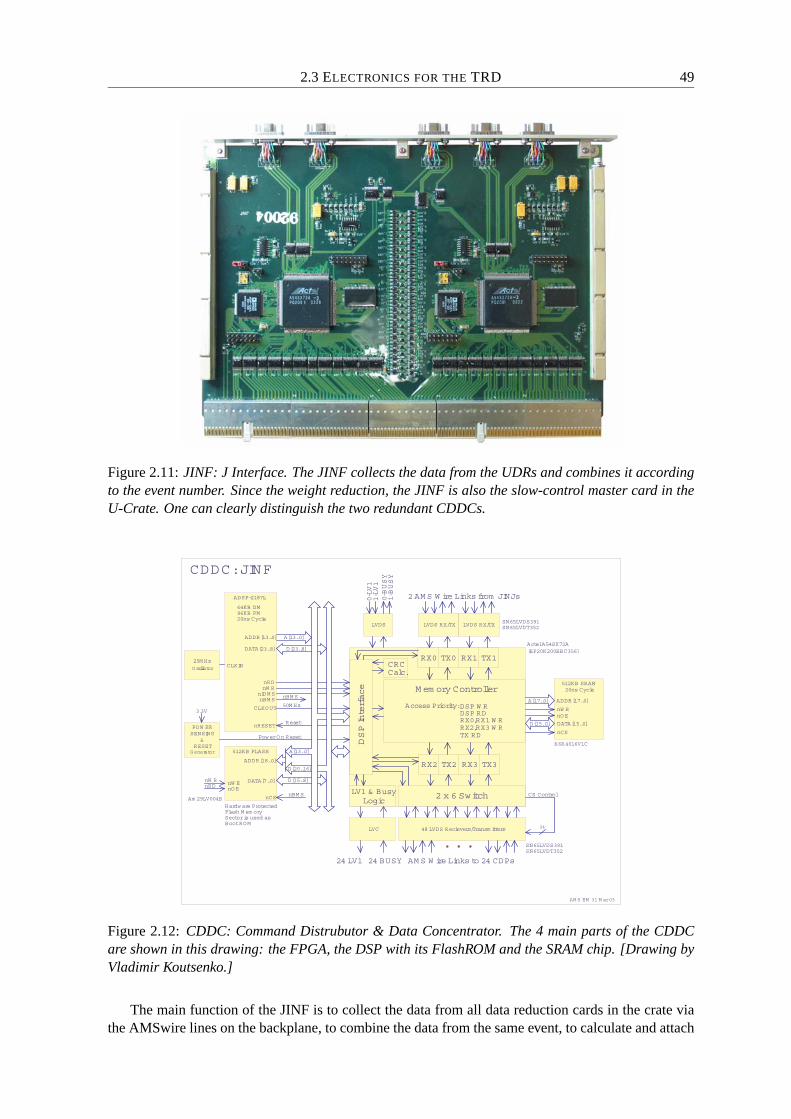
2.3 ELECTRONICS FOR THE TRD 49
Figure 2.11: JINF: J Interface. The JINF collects the data from the UDRs and combines it accordingto the event number. Since the weight reduction, the JINF is also the slow-control master card in theU-Crate. One can clearly distinguish the two redundant CDDCs.
CDDC:JINF
ADSP-2187L
ADDR[13..0]
DATA[23..8]
nBM SnIOM S
CLKIN25M Hz
CLKOUT 50M Hz
TX0 TX1RX0 RX1
2 AM S W ire Links from JINJs
512KB FLASH
ADDR[18..0]
D[20..16]
A[13..0]
nCS
D[15..8]DATA[7..0]
nW RnRD
D[23..8]
A[13..0]
512KB SRAM
A[17..0]
D[15..0]
nCS
nOEnW R
20ns CycleM em ory Controller
Access Priority:DSP W RDSP RD
RX2,RX3 W RTX RD
nRESET
PowerOn Reset
POW ERSENSING
3.3V
ActelA54SX72A
64KB DM
20ns Cycle
DSPInterface
LVDS RX/TX LVDS RX/TX
nOEnW EnW R
nRD
RX0,RX1 W R
SN65LVDS391SN65LVDT352
0-LV1
0-BUSY
ADDR[17..0]
DATA[15..0]
nBM S
nBM S
1-LV1
LVDS
RESET&
(EP20K200EBC356)
Reset
Hardw are ProtectedFlash M em orySectoris used asBootROM
Am 29LV004B
K6R4016V1C
96KB PM
AM S W ire Links to 24 CDPs
24
CS Control2 x 6 Switch
SN65LVDS391SN65LVDT352
1-BUSY
TX2 TX3RX2 RX3
48 LVDS Recievers/Transm ittersLVC
24 LV1 24 BUSY
CRCCalc.
LV1 & BusyLogic
AM S EM 31 M ar03
G enerator
O szillator
Figure 2.12: CDDC: Command Distrubutor & Data Concentrator. The 4 main parts of the CDDCare shown in this drawing: the FPGA, the DSP with its FlashROM and the SRAM chip. [Drawing byVladimir Koutsenko.]
The main function of the JINF is to collect the data from all data reduction cards in the crate viathe AMSwire lines on the backplane, to combine the data from the same event, to calculate and attach
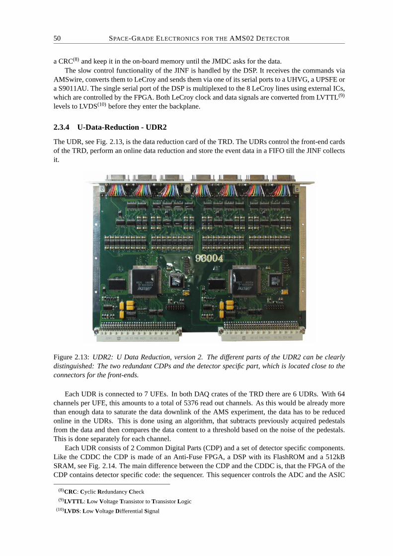
50 SPACE-GRADE ELECTRONICS FOR THE AMS02 DETECTOR
a CRC(8) and keep it in the on-board memory until the JMDC asks for the data.The slow control functionality of the JINF is handled by the DSP. It receives the commands via
AMSwire, converts them to LeCroy and sends them via one of its serial ports to a UHVG, a UPSFE ora S9011AU. The single serial port of the DSP is multiplexed to the 8 LeCroy lines using external ICs,which are controlled by the FPGA. Both LeCroy clock and data signals are converted from LVTTL(9)
levels to LVDS(10) before they enter the backplane.
2.3.4 U-Data-Reduction - UDR2
The UDR, see Fig. 2.13, is the data reduction card of the TRD. The UDRs control the front-end cardsof the TRD, perform an online data reduction and store the event data in a FIFO till the JINF collectsit.
Figure 2.13: UDR2: U Data Reduction, version 2. The different parts of the UDR2 can be clearlydistinguished: The two redundant CDPs and the detector specific part, which is located close to theconnectors for the front-ends.
Each UDR is connected to 7 UFEs. In both DAQ crates of the TRD there are 6 UDRs. With 64channels per UFE, this amounts to a total of 5376 read out channels. As this would be already morethan enough data to saturate the data downlink of the AMS experiment, the data has to be reducedonline in the UDRs. This is done using an algorithm, that subtracts previously acquired pedestalsfrom the data and then compares the data content to a threshold based on the noise of the pedestals.This is done separately for each channel.
Each UDR consists of 2 Common Digital Parts (CDP) and a set of detector specific components.Like the CDDC the CDP is made of an Anti-Fuse FPGA, a DSP with its FlashROM and a 512kBSRAM, see Fig. 2.14. The main difference between the CDP and the CDDC is, that the FPGA of theCDP contains detector specific code: the sequencer. This sequencer controls the ADC and the ASIC
(8)CRC: Cyclic Redundancy Check(9)LVTTL: Low Voltage Transistor to Transistor Logic
(10)LVDS: Low Voltage Differential Signal
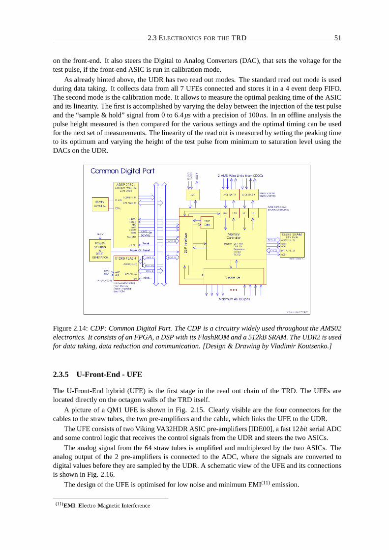
2.3 ELECTRONICS FOR THE TRD 51
on the front-end. It also steers the Digital to Analog Converters (DAC), that sets the voltage for thetest pulse, if the front-end ASIC is run in calibration mode.
As already hinted above, the UDR has two read out modes. The standard read out mode is usedduring data taking. It collects data from all 7 UFEs connected and stores it in a 4 event deep FIFO.The second mode is the calibration mode. It allows to measure the optimal peaking time of the ASICand its linearity. The first is accomplished by varying the delay between the injection of the test pulseand the “sample & hold” signal from 0 to 6.4µs with a precision of 100ns. In an offline analysis thepulse height measured is then compared for the various settings and the optimal timing can be usedfor the next set of measurements. The linearity of the read out is measured by setting the peaking timeto its optimum and varying the height of the test pulse from minimum to saturation level using theDACs on the UDR.
Figure 2.14: CDP: Common Digital Part. The CDP is a circuitry widely used throughout the AMS02electronics. It consists of an FPGA, a DSP with its FlashROM and a 512kB SRAM. The UDR2 is usedfor data taking, data reduction and communication. [Design & Drawing by Vladimir Koutsenko.]
2.3.5 U-Front-End - UFE
The U-Front-End hybrid (UFE) is the first stage in the read out chain of the TRD. The UFEs arelocated directly on the octagon walls of the TRD itself.
A picture of a QM1 UFE is shown in Fig. 2.15. Clearly visible are the four connectors for thecables to the straw tubes, the two pre-amplifiers and the cable, which links the UFE to the UDR.
The UFE consists of two Viking VA32HDR ASIC pre-amplifiers [IDE00], a fast 12bit serial ADCand some control logic that receives the control signals from the UDR and steers the two ASICs.
The analog signal from the 64 straw tubes is amplified and multiplexed by the two ASICs. Theanalog output of the 2 pre-amplifiers is connected to the ADC, where the signals are converted todigital values before they are sampled by the UDR. A schematic view of the UFE and its connectionsis shown in Fig. 2.16.
The design of the UFE is optimised for low noise and minimum EMI(11) emission.
(11)EMI: Electro-Magnetic Interference
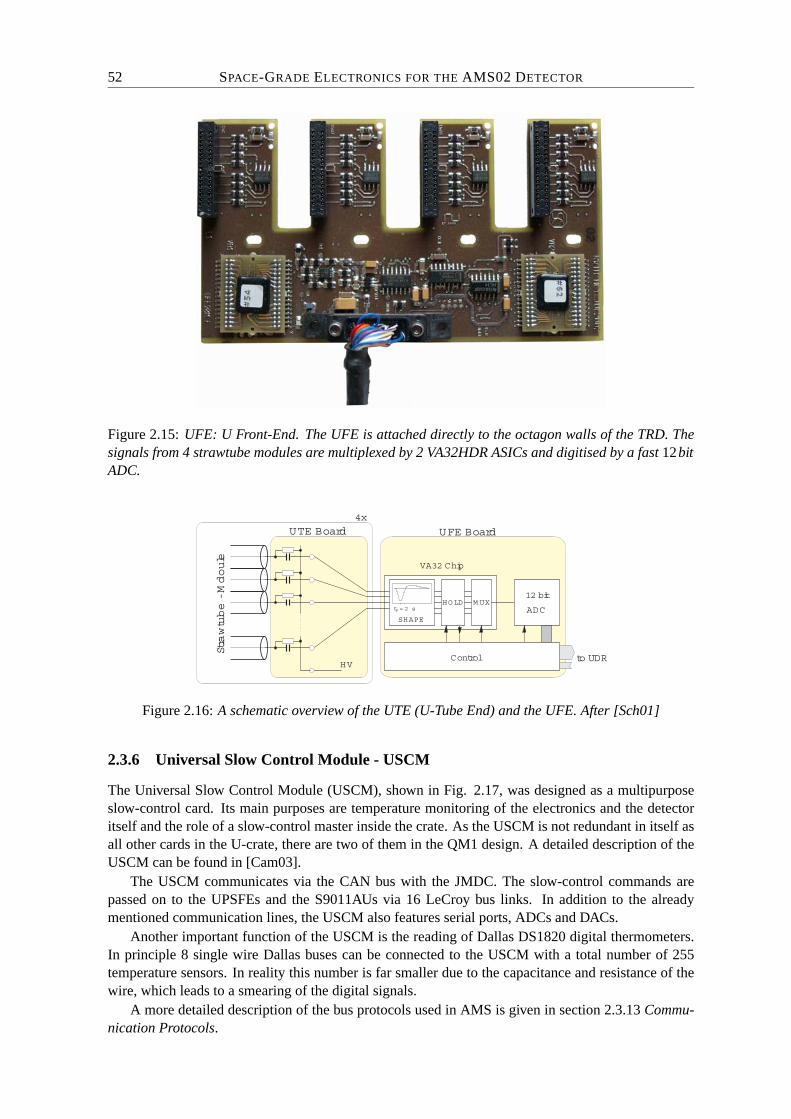
52 SPACE-GRADE ELECTRONICS FOR THE AMS02 DETECTOR
Figure 2.15: UFE: U Front-End. The UFE is attached directly to the octagon walls of the TRD. Thesignals from 4 strawtube modules are multiplexed by 2 VA32HDR ASICs and digitised by a fast 12bitADC.
t = 2 sP ADC
12 bit
SHAPE
HOLD M UX
VA32 Chip
ControlHV
UTE Board UFE Board
to UDR
Strawtube - Mdoule
4x
Figure 2.16: A schematic overview of the UTE (U-Tube End) and the UFE. After [Sch01]
2.3.6 Universal Slow Control Module - USCM
The Universal Slow Control Module (USCM), shown in Fig. 2.17, was designed as a multipurposeslow-control card. Its main purposes are temperature monitoring of the electronics and the detectoritself and the role of a slow-control master inside the crate. As the USCM is not redundant in itself asall other cards in the U-crate, there are two of them in the QM1 design. A detailed description of theUSCM can be found in [Cam03].
The USCM communicates via the CAN bus with the JMDC. The slow-control commands arepassed on to the UPSFEs and the S9011AUs via 16 LeCroy bus links. In addition to the alreadymentioned communication lines, the USCM also features serial ports, ADCs and DACs.
Another important function of the USCM is the reading of Dallas DS1820 digital thermometers.In principle 8 single wire Dallas buses can be connected to the USCM with a total number of 255temperature sensors. In reality this number is far smaller due to the capacitance and resistance of thewire, which leads to a smearing of the digital signals.
A more detailed description of the bus protocols used in AMS is given in section 2.3.13 Commu-nication Protocols.

2.3 ELECTRONICS FOR THE TRD 53
Figure 2.17: USCM: Universal Slow Control Module. Before the weight reduction, the USCM was theslow-control master for the U-Crate. It acted as interface from CAN bus to LeCroy bus and read theDS18S20 temperature sensors on the various cards and in the TRD itself, now these functionalitiesare taken over by other cards.
As stringent limits on the weight of the electronics of the experiment were exceeded, it was neces-sary to save weight by omitting some cards in the various read out crates. One of the cards that wasremoved from the crates was the USCM. Only very few USCMs located in critical places of AMS02remained.
The functionality of the USCMs removed from the DAQ crates was transferred to other cards. Thetemperature monitoring is now done by the few remaining USCMs. The slow-control functions weremoved to the JINF. For a more detailed description please refer to the section on the JINF on page 48.
2.3.7 U-High-Voltage-Generator - UHVG
The UHVG generates the high voltages for the strawtube modules from a 120V input coming from aS9056 DC/DC converter. The output voltage can be set from a few Volts up to ∼ 1850V with 14bitprecision. The principle used on the UHVG is a 16 stage charge pump based on the Cockroft-Waltonmultiplier [Coc32]. Each of these charge pumps is controlled by a LeCroy MHV100 chip [LeC97],a custom development for the AMS experiments. The Cockroft-Walton multipliers and the controlchips are clearly visible in Fig. 2.18.
One UHVG has 14 independent HV channels, which are organised in two groups with sevenchannels each. One of these halves is kept as cold redundant spare during nominal operation. This iscontrolled and monitored by the UPSFEv2. The communication with the two parts of the UHVG isdone via two independent LeCroy links coming from the JINFv2.
Due to the many features of the MHV100 chips the UHVG has a lot of functionality. For eachchannel the UHVG has the possibility to set over-voltage and over-current limits with 16bit precision,which can be also used for an automatic power down of a channel in case of a spark in the strawtube.The actual voltage and current can be read back, as well as the temperature of the device.
The communication with the MHV100 chips on the UHVG is done using the so-called LeCroyprotocol. This protocol uses one data and one clock line for the data transfer. A more detaileddescription of the protocol can be found in section 2.3.13 and in [LeC97].
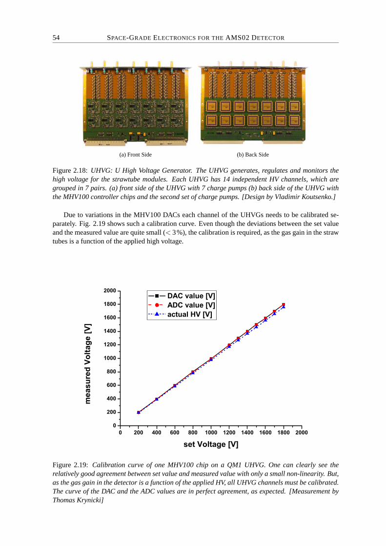
54 SPACE-GRADE ELECTRONICS FOR THE AMS02 DETECTOR
(a) Front Side (b) Back Side
Figure 2.18: UHVG: U High Voltage Generator. The UHVG generates, regulates and monitors thehigh voltage for the strawtube modules. Each UHVG has 14 independent HV channels, which aregrouped in 7 pairs. (a) front side of the UHVG with 7 charge pumps (b) back side of the UHVG withthe MHV100 controller chips and the second set of charge pumps. [Design by Vladimir Koutsenko.]
Due to variations in the MHV100 DACs each channel of the UHVGs needs to be calibrated se-parately. Fig. 2.19 shows such a calibration curve. Even though the deviations between the set valueand the measured value are quite small (< 3%), the calibration is required, as the gas gain in the strawtubes is a function of the applied high voltage.
Figure 2.19: Calibration curve of one MHV100 chip on a QM1 UHVG. One can clearly see therelatively good agreement between set value and measured value with only a small non-linearity. But,as the gas gain in the detector is a function of the applied HV, all UHVG channels must be calibrated.The curve of the DAC and the ADC values are in perfect agreement, as expected. [Measurement byThomas Krynicki]
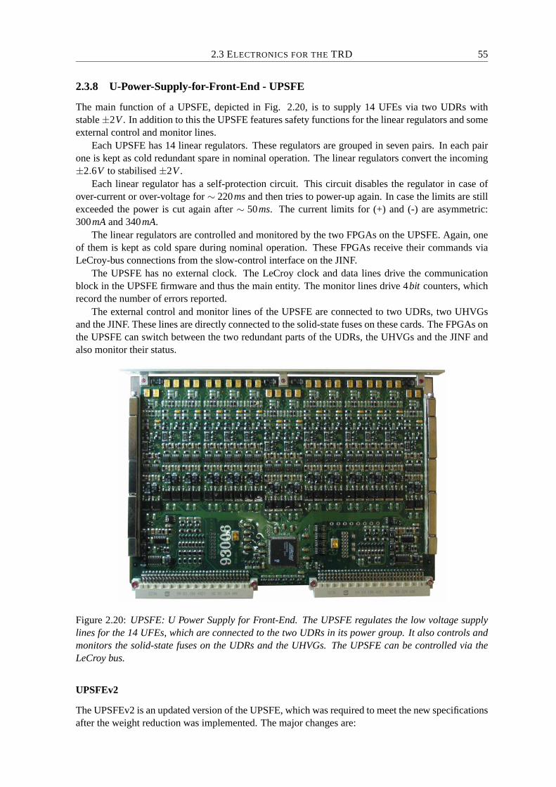
2.3 ELECTRONICS FOR THE TRD 55
2.3.8 U-Power-Supply-for-Front-End - UPSFE
The main function of a UPSFE, depicted in Fig. 2.20, is to supply 14 UFEs via two UDRs withstable ±2V . In addition to this the UPSFE features safety functions for the linear regulators and someexternal control and monitor lines.
Each UPSFE has 14 linear regulators. These regulators are grouped in seven pairs. In each pairone is kept as cold redundant spare in nominal operation. The linear regulators convert the incoming±2.6V to stabilised ±2V .
Each linear regulator has a self-protection circuit. This circuit disables the regulator in case ofover-current or over-voltage for ∼ 220ms and then tries to power-up again. In case the limits are stillexceeded the power is cut again after ∼ 50ms. The current limits for (+) and (-) are asymmetric:300mA and 340mA.
The linear regulators are controlled and monitored by the two FPGAs on the UPSFE. Again, oneof them is kept as cold spare during nominal operation. These FPGAs receive their commands viaLeCroy-bus connections from the slow-control interface on the JINF.
The UPSFE has no external clock. The LeCroy clock and data lines drive the communicationblock in the UPSFE firmware and thus the main entity. The monitor lines drive 4bit counters, whichrecord the number of errors reported.
The external control and monitor lines of the UPSFE are connected to two UDRs, two UHVGsand the JINF. These lines are directly connected to the solid-state fuses on these cards. The FPGAs onthe UPSFE can switch between the two redundant parts of the UDRs, the UHVGs and the JINF andalso monitor their status.
Figure 2.20: UPSFE: U Power Supply for Front-End. The UPSFE regulates the low voltage supplylines for the 14 UFEs, which are connected to the two UDRs in its power group. It also controls andmonitors the solid-state fuses on the UDRs and the UHVGs. The UPSFE can be controlled via theLeCroy bus.
UPSFEv2
The UPSFEv2 is an updated version of the UPSFE, which was required to meet the new specificationsafter the weight reduction was implemented. The major changes are:
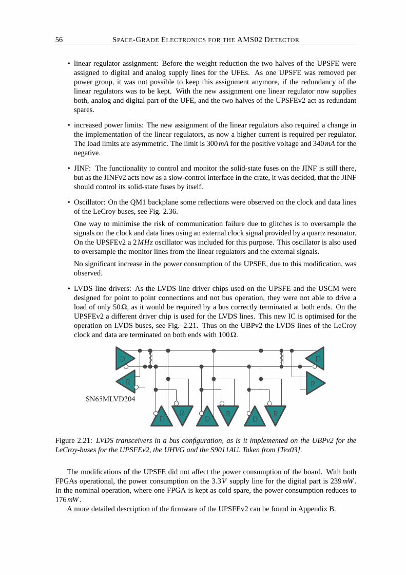
56 SPACE-GRADE ELECTRONICS FOR THE AMS02 DETECTOR
• linear regulator assignment: Before the weight reduction the two halves of the UPSFE wereassigned to digital and analog supply lines for the UFEs. As one UPSFE was removed perpower group, it was not possible to keep this assignment anymore, if the redundancy of thelinear regulators was to be kept. With the new assignment one linear regulator now suppliesboth, analog and digital part of the UFE, and the two halves of the UPSFEv2 act as redundantspares.
• increased power limits: The new assignment of the linear regulators also required a change inthe implementation of the linear regulators, as now a higher current is required per regulator.The load limits are asymmetric. The limit is 300mA for the positive voltage and 340mA for thenegative.
• JINF: The functionality to control and monitor the solid-state fuses on the JINF is still there,but as the JINFv2 acts now as a slow-control interface in the crate, it was decided, that the JINFshould control its solid-state fuses by itself.
• Oscillator: On the QM1 backplane some reflections were observed on the clock and data linesof the LeCroy buses, see Fig. 2.36.
One way to minimise the risk of communication failure due to glitches is to oversample thesignals on the clock and data lines using an external clock signal provided by a quartz resonator.On the UPSFEv2 a 2MHz oscillator was included for this purpose. This oscillator is also usedto oversample the monitor lines from the linear regulators and the external signals.
No significant increase in the power consumption of the UPSFE, due to this modification, wasobserved.
• LVDS line drivers: As the LVDS line driver chips used on the UPSFE and the USCM weredesigned for point to point connections and not bus operation, they were not able to drive aload of only 50Ω, as it would be required by a bus correctly terminated at both ends. On theUPSFEv2 a different driver chip is used for the LVDS lines. This new IC is optimised for theoperation on LVDS buses, see Fig. 2.21. Thus on the UBPv2 the LVDS lines of the LeCroyclock and data are terminated on both ends with 100Ω.
D
R
R
D
RR
D
RD R
D
RD
R
D
D
SN65MLVD204
Figure 2.21: LVDS transceivers in a bus configuration, as is it implemented on the UBPv2 for theLeCroy-buses for the UPSFEv2, the UHVG and the S9011AU. Taken from [Tex03].
The modifications of the UPSFE did not affect the power consumption of the board. With bothFPGAs operational, the power consumption on the 3.3V supply line for the digital part is 239mW .In the nominal operation, where one FPGA is kept as cold spare, the power consumption reduces to176mW .
A more detailed description of the firmware of the UPSFEv2 can be found in Appendix B.
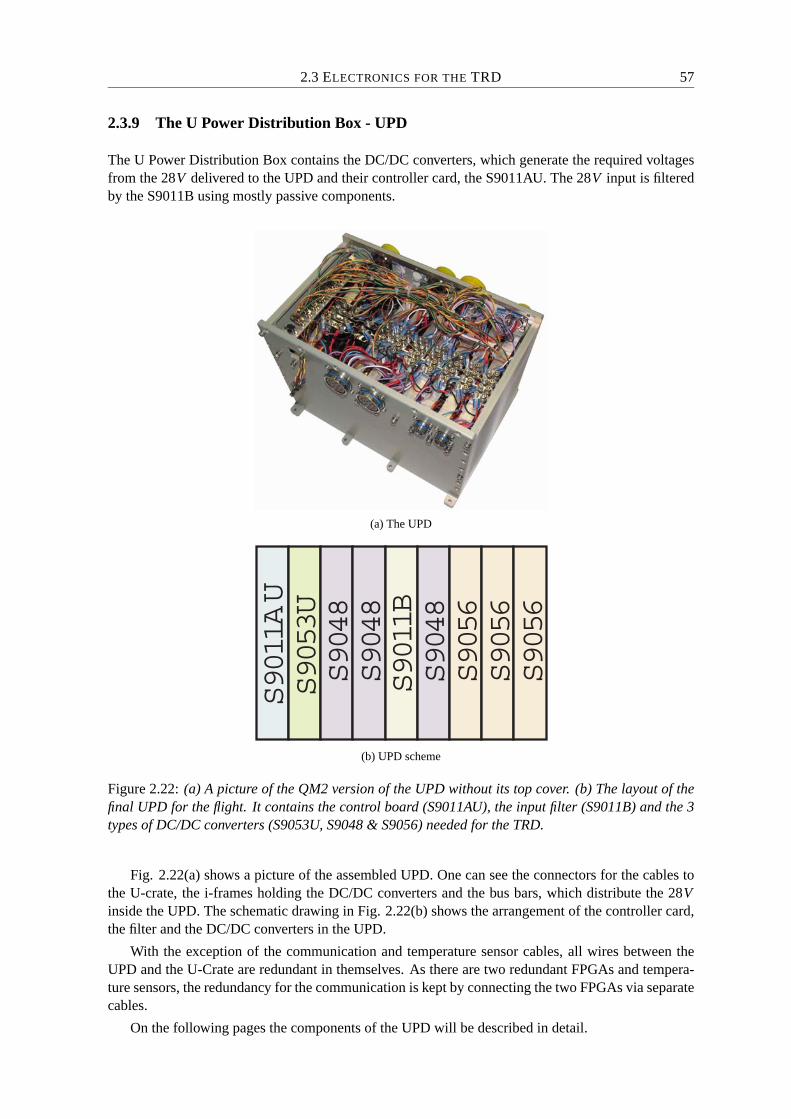
2.3 ELECTRONICS FOR THE TRD 57
2.3.9 The U Power Distribution Box - UPD
The U Power Distribution Box contains the DC/DC converters, which generate the required voltagesfrom the 28V delivered to the UPD and their controller card, the S9011AU. The 28V input is filteredby the S9011B using mostly passive components.
(a) The UPD
S9011AU
S9048
S9048
S9048
S9056
S9053U
S9011B
S9056
S9056
(b) UPD scheme
Figure 2.22: (a) A picture of the QM2 version of the UPD without its top cover. (b) The layout of thefinal UPD for the flight. It contains the control board (S9011AU), the input filter (S9011B) and the 3types of DC/DC converters (S9053U, S9048 & S9056) needed for the TRD.
Fig. 2.22(a) shows a picture of the assembled UPD. One can see the connectors for the cables tothe U-crate, the i-frames holding the DC/DC converters and the bus bars, which distribute the 28Vinside the UPD. The schematic drawing in Fig. 2.22(b) shows the arrangement of the controller card,the filter and the DC/DC converters in the UPD.
With the exception of the communication and temperature sensor cables, all wires between theUPD and the U-Crate are redundant in themselves. As there are two redundant FPGAs and tempera-ture sensors, the redundancy for the communication is kept by connecting the two FPGAs via separatecables.
On the following pages the components of the UPD will be described in detail.
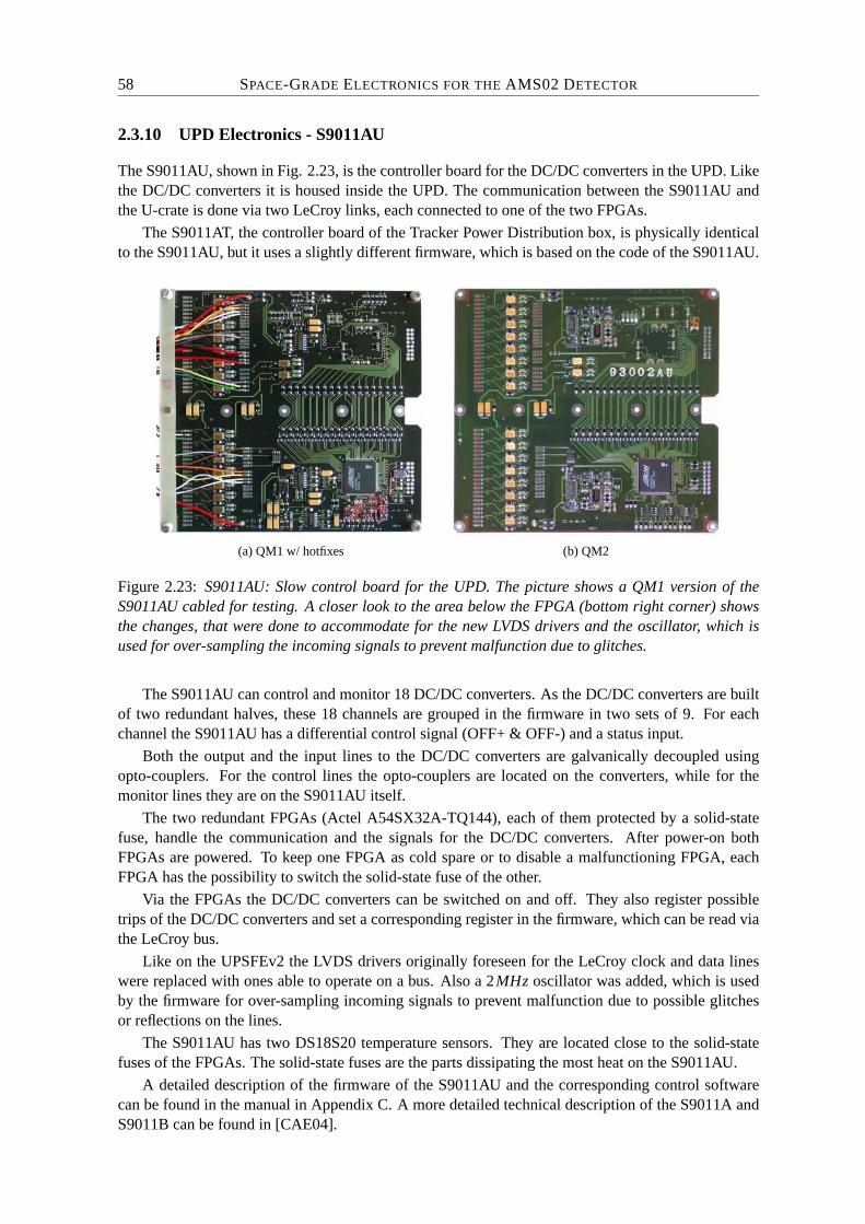
58 SPACE-GRADE ELECTRONICS FOR THE AMS02 DETECTOR
2.3.10 UPD Electronics - S9011AU
The S9011AU, shown in Fig. 2.23, is the controller board for the DC/DC converters in the UPD. Likethe DC/DC converters it is housed inside the UPD. The communication between the S9011AU andthe U-crate is done via two LeCroy links, each connected to one of the two FPGAs.
The S9011AT, the controller board of the Tracker Power Distribution box, is physically identicalto the S9011AU, but it uses a slightly different firmware, which is based on the code of the S9011AU.
(a) QM1 w/ hotfixes (b) QM2
Figure 2.23: S9011AU: Slow control board for the UPD. The picture shows a QM1 version of theS9011AU cabled for testing. A closer look to the area below the FPGA (bottom right corner) showsthe changes, that were done to accommodate for the new LVDS drivers and the oscillator, which isused for over-sampling the incoming signals to prevent malfunction due to glitches.
The S9011AU can control and monitor 18 DC/DC converters. As the DC/DC converters are builtof two redundant halves, these 18 channels are grouped in the firmware in two sets of 9. For eachchannel the S9011AU has a differential control signal (OFF+ & OFF-) and a status input.
Both the output and the input lines to the DC/DC converters are galvanically decoupled usingopto-couplers. For the control lines the opto-couplers are located on the converters, while for themonitor lines they are on the S9011AU itself.
The two redundant FPGAs (Actel A54SX32A-TQ144), each of them protected by a solid-statefuse, handle the communication and the signals for the DC/DC converters. After power-on bothFPGAs are powered. To keep one FPGA as cold spare or to disable a malfunctioning FPGA, eachFPGA has the possibility to switch the solid-state fuse of the other.
Via the FPGAs the DC/DC converters can be switched on and off. They also register possibletrips of the DC/DC converters and set a corresponding register in the firmware, which can be read viathe LeCroy bus.
Like on the UPSFEv2 the LVDS drivers originally foreseen for the LeCroy clock and data lineswere replaced with ones able to operate on a bus. Also a 2MHz oscillator was added, which is usedby the firmware for over-sampling incoming signals to prevent malfunction due to possible glitchesor reflections on the lines.
The S9011AU has two DS18S20 temperature sensors. They are located close to the solid-statefuses of the FPGAs. The solid-state fuses are the parts dissipating the most heat on the S9011AU.
A detailed description of the firmware of the S9011AU and the corresponding control softwarecan be found in the manual in Appendix C. A more detailed technical description of the S9011A andS9011B can be found in [CAE04].
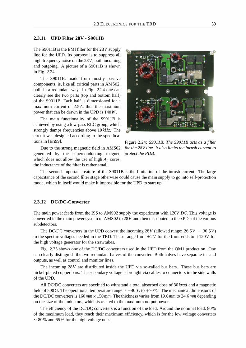
2.3 ELECTRONICS FOR THE TRD 59
2.3.11 UPD Filter 28V - S9011B
Figure 2.24: S9011B: The S9011B acts as a filterfor the 28V line. It also limits the inrush current toprotect the PDB.
The S9011B is the EMI filter for the 28V supplyline for the UPD. Its purpose is to suppress allhigh frequency noise on the 28V , both incomingand outgoing. A picture of a S9011B is shownin Fig. 2.24.
The S9011B, made from mostly passivecomponents, is, like all critical parts in AMS02,built in a redundant way. In Fig. 2.24 one canclearly see the two parts (top and bottom half)of the S9011B. Each half is dimensioned for amaximum current of 2.5A, thus the maximumpower that can be drawn in the UPD is 140W .
The main functionality of the S9011B isachieved by using a low-pass RLC group, whichstrongly damps frequencies above 10kHz. Thecircuit was designed according to the specifica-tions in [Eri99].
Due to the strong magnetic field in AMS02generated by the superconducting magnet,which does not allow the use of high AL cores,the inductance of the filter is rather small.
The second important feature of the S9011B is the limitation of the inrush current. The largecapacitance of the second filter stage otherwise could cause the main supply to go into self-protectionmode, which in itself would make it impossible for the UPD to start up.
2.3.12 DC/DC-Converter
The main power feeds from the ISS to AMS02 supply the experiment with 120V DC. This voltage isconverted in the main power system of AMS02 to 28V and then distributed to the xPDs of the varioussubdetectors.
The DC/DC converters in the UPD convert the incoming 28V (allowed range: 26.5V − 30.5V )to the specific voltages needed in the TRD. These range from ±2V for the front-ends to +120V forthe high voltage generator for the strawtubes.
Fig. 2.25 shows one of the DC/DC converters used in the UPD from the QM1 production. Onecan clearly distinguish the two redundant halves of the converter. Both halves have separate in- andoutputs, as well as control and monitor lines.
The incoming 28V are distributed inside the UPD via so-called bus bars. These bus bars arenickel-plated copper bars. The secondary voltage is brought via cables to connectors in the side wallsof the UPD.
All DC/DC converters are specified to withstand a total absorbed dose of 30krad and a magneticfield of 500G. The operational temperature range is −40 C to +70 C. The mechanical dimensions ofthe DC/DC converters is 160mm×150mm. The thickness varies from 19.6mm to 24.6mm dependingon the size of the inductors, which is related to the maximum output power.
The efficiency of the DC/DC converters is a function of the load. Around the nominal load, 80%of the maximum load, they reach their maximum efficiency, which is for the low voltage converters∼ 80% and 65% for the high voltage ones.
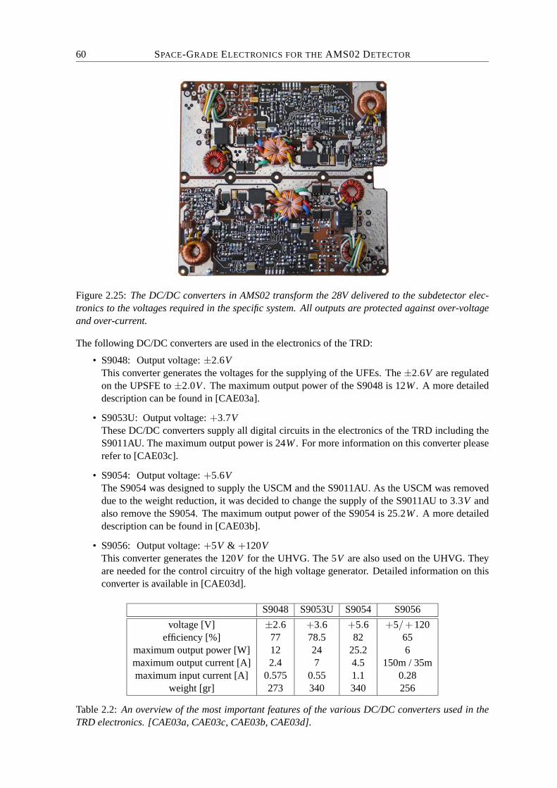
60 SPACE-GRADE ELECTRONICS FOR THE AMS02 DETECTOR
Figure 2.25: The DC/DC converters in AMS02 transform the 28V delivered to the subdetector elec-tronics to the voltages required in the specific system. All outputs are protected against over-voltageand over-current.
The following DC/DC converters are used in the electronics of the TRD:
• S9048: Output voltage: ±2.6VThis converter generates the voltages for the supplying of the UFEs. The ±2.6V are regulatedon the UPSFE to ±2.0V . The maximum output power of the S9048 is 12W . A more detaileddescription can be found in [CAE03a].
• S9053U: Output voltage: +3.7VThese DC/DC converters supply all digital circuits in the electronics of the TRD including theS9011AU. The maximum output power is 24W . For more information on this converter pleaserefer to [CAE03c].
• S9054: Output voltage: +5.6VThe S9054 was designed to supply the USCM and the S9011AU. As the USCM was removeddue to the weight reduction, it was decided to change the supply of the S9011AU to 3.3V andalso remove the S9054. The maximum output power of the S9054 is 25.2W . A more detaileddescription can be found in [CAE03b].
• S9056: Output voltage: +5V & +120VThis converter generates the 120V for the UHVG. The 5V are also used on the UHVG. Theyare needed for the control circuitry of the high voltage generator. Detailed information on thisconverter is available in [CAE03d].
S9048 S9053U S9054 S9056
voltage [V] ±2.6 +3.6 +5.6 +5/+120efficiency [%] 77 78.5 82 65
maximum output power [W] 12 24 25.2 6maximum output current [A] 2.4 7 4.5 150m / 35mmaximum input current [A] 0.575 0.55 1.1 0.28
weight [gr] 273 340 340 256
Table 2.2: An overview of the most important features of the various DC/DC converters used in theTRD electronics. [CAE03a, CAE03c, CAE03b, CAE03d].
2.3 ELECTRONICS FOR THE TRD 61
2.3.13 Communication Protocols
In the AMS02 experiment various types of communication protocols are used: From the high speeddata link AMSwire to the low speed LeCroy bus for slow control functions. In the following sections ashort description will be given for each of the 3 protocols used in the TRD. For a more comprehensivereading please refer to the references given for each protocol.
AMSwire
AMSwire is a point-to-point serial link operated at 50MHz in a master and slave mode. It is used onall levels of the DAQ chain in AMS02. The Double-Data-Rate and a small overhead in the protocolallow for a net data transfer rate of 10MByte/s. Together with the very low latency this makes theprotocol ideal for transferring the scientific data inside the experiment.
AMSwire uses four wires for the data transfer. Two wires are used for the receiver (RX) and twofor the transmitter (TX). For each direction there is one data line and one strobe line. The clock isreconstructed in the receiver by “XORing” the signals from the data and the strobe lines. There arealso separate buffers for RX and TX.
To ensure maximum safety for the transmission, the lines are implemented as LVDS connectionsand there are always at least two independent links between to partners.
Since the weight reduction in the electronics of the AMS02 electronics, the AMSwire protocol isnot exclusively used for the data acquisition any more, but also for the slow-control data.
The AMSwire protocol and implementation [LIN03] are a development of the AMS collaborationbased on the SpaceWire [ECS03], which itself is based on the IEEE-1355 standard [IEE95].
CAN-Bus
The CAN-bus(12) was defined in the 1980s by the Robert Bosch GmbH [Bos91]. It was designed forreal-time safety-critical applications like in the automotive environment. By now it has become anindustrial standard (ISO 11898) and is used in a lot of different applications.
The CAN-bus is a multi-master bus specified for a maximum length of 40m and a data rate of upto 1Mbit/s. In the AMS02 experiment it is used in the slow-control system to connect the USCMs inthe various crates to the main DAQ computer.
Using 2-wire differential connections and a set of error detection mechanisms the CAN-bus isextremely failure safe and can “survive” even a failure on one of the two wires.
As the USCMs were removed from the U-crate during the weight reduction and the functionalitywas taken over by the JINFv2, the CAN-bus is not used anymore in the TRD read out electronicsfrom the QM2 version of the electronics onwards. All slow-control data is now transmitted using theAMSwire protocol. In other subdetectors, where there is still a USCM, the CAN-bus is still in usage.
LeCroy bus
The LeCroy bus was designed by the LeCroy Corporation for the digital data interface of the highvoltage chip MHV100 [LeC97], which is used on the UHVG. In AMS02 the LeCroy bus is used forthe communication on the lowest level of the slow-control system in various places.
In the TRD electronics the LeCroy bus is used for the communication between the USCM / JINFv2and the slow-control slaves: UHVG, UPSFEv2 and S9011AU. The bi-directional LeCroy bus consistsof one data and one clock line.
The communication is always initiated by the bus master (e.g. JINFv2). In the first 32 bits of thecommunication a command is transmitted to the slave (e.g. UPSFEv2), in the second 32 bits the slaveeither sends an echo of the command or the reply in case of a read request. A detailed overview of thebit usage in the LeCroy bus communication can be found in Appendix A and in [LeC97].
(12)CAN: Controller Area Network
62 SPACE-GRADE ELECTRONICS FOR THE AMS02 DETECTOR
Dallas 1-wire Bus
The 1-wire bus was developed by Dallas Semiconductor for connecting sensors, like thermometersor pressure probes, to µControllers. The communication in this master-slave bus runs at 16kbps atregular speed and at 140kbps in overdrive mode using CMOS/TTL logic levels.
The 1-wire bus consists of a data line and a ground line. If the bus is operated in parasitic mode,the data line is also used to power the slave devices. This is done using the half-wave rectifiers whichare present in each slave. As buses with a lot of slaves would draw to much power from the masterdriving the line, the slaves can also be powered externally.
As the 1-wire bus has no separate clock and data line, the data transfer is done using the time slotmethod. A system clock is not required for this, as there is an internal oscillator in each device on thebus, which is synchronised to the falling edge of the master.
At the beginning of each command the master resets the bus by pulling it low for at least 480µs,after this it waits for the presence pulses from the slaves. In order to write a logic “1” the master pullsthe bus low for 15µs or less. For a logic “0” the master pulls the bus low for 60µs or more. The timemargin is used to counter any issues due to worst case conditions.
Each 1-wire device is identifiable by a 64bit Device ID. This ID contains a 48bit unique serialnumber, an 8bit device family code and an 8bit CRC.
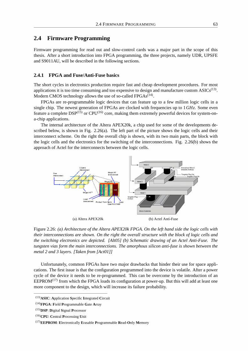
2.4 FIRMWARE PROGRAMMING 63
2.4 Firmware Programming
Firmware programming for read out and slow-control cards was a major part in the scope of thisthesis. After a short introduction into FPGA programming, the three projects, namely UDR, UPSFEand S9011AU, will be described in the following sections.
2.4.1 FPGA and Fuse/Anti-Fuse basics
The short cycles in electronics production require fast and cheap development procedures. For mostapplications it is too time consuming and too expensive to design and manufacture custom ASICs(13).Modern CMOS technology allows the use of so-called FPGAs(14).
FPGAs are re-programmable logic devices that can feature up to a few million logic cells in asingle chip. The newest generation of FPGAs are clocked with frequencies up to 1GHz. Some evenfeature a complete DSP(15) or CPU(16) core, making them extremely powerful devices for system-on-a-chip applications.
The internal architecture of the Altera APEX20k, a chip used for some of the developments de-scribed below, is shown in Fig. 2.26(a). The left part of the picture shows the logic cells and theirinterconnect scheme. On the right the overall chip is shown, with its two main parts, the block withthe logic cells and the electronics for the switching of the interconnections. Fig. 2.26(b) shows theapproach of Actel for the interconnects between the logic cells.
(a) Altera APEX20k (b) Actel Anti-Fuse
Figure 2.26: (a) Architecture of the Altera APEX20k FPGA. On the left hand side the logic cells withtheir interconnections are shown. On the right the overall structure with the block of logic cells andthe switching electronics are depicted. [Alt05] (b) Schematic drawing of an Actel Anti-Fuse. Thetungsten vias form the main interconnections. The amorphous silicon anti-fuse is shown between themetal 2 and 3 layers. [Taken from [Act01]]
Unfortunately, common FPGAs have two major drawbacks that hinder their use for space appli-cations. The first issue is that the configuration programmed into the device is volatile. After a powercycle of the device it needs to be re-programmed. This can be overcome by the introduction of anEEPROM(17) from which the FPGA loads its configuration at power-up. But this will add at least onemore component to the design, which will increase its failure probability.
(13)ASIC: Application Specific Integrated Circuit(14)FPGA: Field Programmable Gate Array(15)DSP: Digital Signal Processor(16)CPU: Central Processing Unit(17)EEPROM: Electronically Erasable Programmable Read-Only Memory
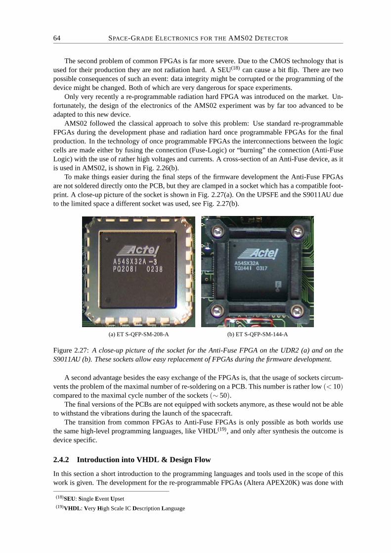
64 SPACE-GRADE ELECTRONICS FOR THE AMS02 DETECTOR
The second problem of common FPGAs is far more severe. Due to the CMOS technology that isused for their production they are not radiation hard. A SEU(18) can cause a bit flip. There are twopossible consequences of such an event: data integrity might be corrupted or the programming of thedevice might be changed. Both of which are very dangerous for space experiments.
Only very recently a re-programmable radiation hard FPGA was introduced on the market. Un-fortunately, the design of the electronics of the AMS02 experiment was by far too advanced to beadapted to this new device.
AMS02 followed the classical approach to solve this problem: Use standard re-programmableFPGAs during the development phase and radiation hard once programmable FPGAs for the finalproduction. In the technology of once programmable FPGAs the interconnections between the logiccells are made either by fusing the connection (Fuse-Logic) or “burning” the connection (Anti-FuseLogic) with the use of rather high voltages and currents. A cross-section of an Anti-Fuse device, as itis used in AMS02, is shown in Fig. 2.26(b).
To make things easier during the final steps of the firmware development the Anti-Fuse FPGAsare not soldered directly onto the PCB, but they are clamped in a socket which has a compatible foot-print. A close-up picture of the socket is shown in Fig. 2.27(a). On the UPSFE and the S9011AU dueto the limited space a different socket was used, see Fig. 2.27(b).
(a) ET S-QFP-SM-208-A (b) ET S-QFP-SM-144-A
Figure 2.27: A close-up picture of the socket for the Anti-Fuse FPGA on the UDR2 (a) and on theS9011AU (b). These sockets allow easy replacement of FPGAs during the firmware development.
A second advantage besides the easy exchange of the FPGAs is, that the usage of sockets circum-vents the problem of the maximal number of re-soldering on a PCB. This number is rather low (< 10)compared to the maximal cycle number of the sockets (∼ 50).
The final versions of the PCBs are not equipped with sockets anymore, as these would not be ableto withstand the vibrations during the launch of the spacecraft.
The transition from common FPGAs to Anti-Fuse FPGAs is only possible as both worlds usethe same high-level programming languages, like VHDL(19), and only after synthesis the outcome isdevice specific.
2.4.2 Introduction into VHDL & Design Flow
In this section a short introduction to the programming languages and tools used in the scope of thiswork is given. The development for the re-programmable FPGAs (Altera APEX20K) was done with
(18)SEU: Single Event Upset(19)VHDL: Very High Scale IC Description Language
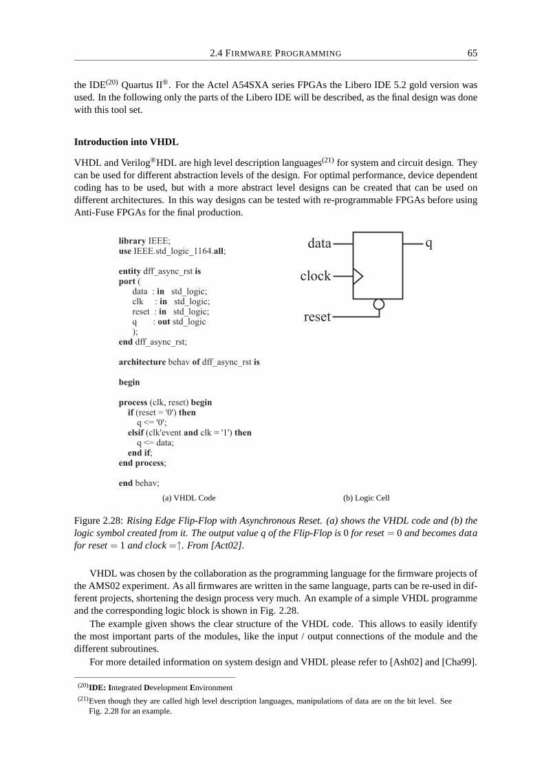
2.4 FIRMWARE PROGRAMMING 65
the IDE(20) Quartus II®. For the Actel A54SXA series FPGAs the Libero IDE 5.2 gold version wasused. In the following only the parts of the Libero IDE will be described, as the final design was donewith this tool set.
Introduction into VHDL
VHDL and Verilog®HDL are high level description languages(21) for system and circuit design. Theycan be used for different abstraction levels of the design. For optimal performance, device dependentcoding has to be used, but with a more abstract level designs can be created that can be used ondifferent architectures. In this way designs can be tested with re-programmable FPGAs before usingAnti-Fuse FPGAs for the final production.
libraryuse all
entity isport
inout
end
architecture of is
begin
process beginif then
elsif and then
end ifend process
end
IEEE;IEEE.std_logic_1164. ;
dff_async_rst(
dataclkreset : std_logic;q : std_logic);dff_async_rst;
behav dff_async_rst
(clk, reset)(reset = '0')q <= '0';
(clk'event clk = '1')q <= data;
;;
behav;
: std_logic;: std_logic;inin
(a) VHDL Code
data
clock
reset
q
(b) Logic Cell
Figure 2.28: Rising Edge Flip-Flop with Asynchronous Reset. (a) shows the VHDL code and (b) thelogic symbol created from it. The output value q of the Flip-Flop is 0 for reset = 0 and becomes datafor reset = 1 and clock =↑. From [Act02].
VHDL was chosen by the collaboration as the programming language for the firmware projects ofthe AMS02 experiment. As all firmwares are written in the same language, parts can be re-used in dif-ferent projects, shortening the design process very much. An example of a simple VHDL programmeand the corresponding logic block is shown in Fig. 2.28.
The example given shows the clear structure of the VHDL code. This allows to easily identifythe most important parts of the modules, like the input / output connections of the module and thedifferent subroutines.
For more detailed information on system design and VHDL please refer to [Ash02] and [Cha99].
(20)IDE: Integrated Development Environment(21)Even though they are called high level description languages, manipulations of data are on the bit level. See
Fig. 2.28 for an example.

66 SPACE-GRADE ELECTRONICS FOR THE AMS02 DETECTOR
Design flow
In the following section the design flow from the conceptual draft to the final file programmed intothe FPGA will be explained.
• Conceptual design: This is the first stage of the design of a new firmware. As a first step thenecessary functions and communication protocols are defined on a very abstract level. Afterthis the most important parts and their connections to each other and the outside world areidentified. These major parts define the structure of the VHDL code.
• VHDL design: The main entity and its different sub-components are put into VHDL code. Inthis step the project is still device independent and can be used on many different chip architec-tures.
• Synthesis: When the first iteration of the VHDL code is ready for further processing the syn-thesis is started. In this process the functionality described in the VHDL code is mapped todevice specific logic cells and gates in the FPGA. In case of too little resources in the FPGA, apossible optimisation is to allow the synthesis tool to re-use the same logical cell for differentpurposes, thus decreasing the total number of cells needed.
The log file of the synthesis tool gives very detailed information about the number of logicalcells used in the project. It also provides first timing estimates on the design allowing re-considerations before going to the next stage of the design.
• Compilation: In this stage the result of the synthesis is used to extract the information on thenumber of IO pins and logic cells used in the design. Also the use of the various clock networksis verified.
• Pin Assignment: Once the software has extracted the information on the IO signals used,these signals have to be assigned to pins of the FPGA to connect the internal functions of thedesign to the outside world, the PCB.
But not only has the signal to be assigned to the correct pin, but also the corresponding IOstandard (e.g. LVTTL, CMOS or PCI) has to be selected. As an additional setting it is alsopossible to select the default value of a pin after powering the device. Also the external clocksare connected to the corresponding internal clock networks in this stage of the design flow.
• Layout: After selecting the pins, the development tool can assign the logic cells from thesynthesis to the physical cells in the FPGA.
Different optimisation levels can be selected for this process. The development tool used forthe Actel Anti-Fuse FPGAs has three optimisation levels: Incremental placement, timing drivenplacement and multiple iterations. These three optimisations can be combined to achieve betterresults.
• Netlist: The netlist is a result from the layout process. It can be used to check if the IDEassigned the correct logical cells to the desired functions and if they are connected accordingly.
• Back Annotation: The timing extractor generates the back annotation file from the output ofthe layout. It uses an internal database to calculate the delays of the different logical cells andthe interconnects along the paths of the internal signals.
• Stimulus: Using a waveform generator a stimulus file is created. In this stimulus file the valuesof the external signals going into the FPGA are listed as a function of the time. The achievableprecision is 1 ps.
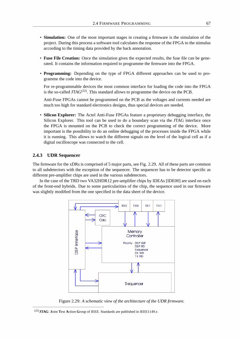
2.4 FIRMWARE PROGRAMMING 67
• Simulation: One of the most important stages in creating a firmware is the simulation of theproject. During this process a software tool calculates the response of the FPGA to the stimulusaccording to the timing data provided by the back annotation.
• Fuse File Creation: Once the simulation gives the expected results, the fuse file can be gene-rated. It contains the information required to programme the firmware into the FPGA.
• Programming: Depending on the type of FPGA different approaches can be used to pro-gramme the code into the device.
For re-programmable devices the most common interface for loading the code into the FPGAis the so-called JTAG(22). This standard allows to programme the device on the PCB.
Anti-Fuse FPGAs cannot be programmed on the PCB as the voltages and currents needed aremuch too high for standard electronics designs, thus special devices are needed.
• Silicon Explorer: The Actel Anti-Fuse FPGAs feature a proprietary debugging interface, theSilicon Explorer. This tool can be used to do a boundary scan via the JTAG interface oncethe FPGA is mounted on the PCB to check the correct programming of the device. Moreimportant is the possibility to do an online debugging of the processes inside the FPGA whileit is running. This allows to watch the different signals on the level of the logical cell as if adigital oscilloscope was connected to the cell.
2.4.3 UDR Sequencer
The firmware for the xDRs is comprised of 5 major parts, see Fig. 2.29. All of these parts are commonto all subdetectors with the exception of the sequencer. The sequencer has to be detector specific asdifferent pre-amplifier chips are used in the various subdetectors.
In the case of the TRD two VA32HDR12 pre-amplifier chips by IDEAs [IDE00] are used on eachof the front-end hybrids. Due to some particularities of the chip, the sequence used in our firmwarewas slightly modified from the one specified in the data sheet of the device.
Figure 2.29: A schematic view of the architecture of the UDR firmware.
(22)JTAG: Joint Test Action Group of IEEE. Standards are published in IEEE1149.x

68 SPACE-GRADE ELECTRONICS FOR THE AMS02 DETECTOR
The development process for the sequencer code was separated into 3 phases. In the first phase,the prototyping stage, the code was developed and tested on the S9007. The S9007 has a completeCDP on-board and detector specific add-ons were connected as piggy-backs, see Fig. 2.30(b).
The communication to the PC was done using an EPP(23) cable. The setup used for this first stageis shown in Fig. 2.30(a). On the Linux-PC the data was read into a LabView 6i VI via a C++ library.
(a) Table Top Setup (b) S9007 “Guidoboard”
Figure 2.30: (a) The table top setup for developing the sequencer code. (b) The S9007, often called the“Guidoboard”. With the help of this setup the sequence for the read out and calibration of the front-end amplifier ASIC was implemented in VHDL. The measurements done include timing and linearityscans and energy spectra of various radioactive sources like 55Fe and 90Sr .
The second stage of the development was done using the Engineering Module (EM) version ofthe UDR. Again the FPGA was re-programmable, thus allowing for easy modifications of the code.
The finale phase was done on a QM1 UDR2. As the UDR2 uses an Anti-Fuse FPGA it wasdecided to use a footprint compatible socket for the FPGA to allow easy replacement of the onceprogrammable FPGA during finalisation of the firmware code. A close-up picture of the socket isshown in Fig. 2.27(a).
Two modes are implemented in the UDR2 for reading out the front-end chips: The standard readout mode and the calibration mode. The first mode is used to read the chips during normal datataking. The second mode allows to inject charge via an external capacitor into the input stages of thepre-amplifier chip and thus to calibrate the gain and the linearity of the read out chain.
Fig. 2.31 shows an example of a read out cycle as it is implemented within the firmware of theUDR sequencer. After an incoming trigger the sample & hold signal is sent to the front-end chip.Then the output multiplexers of the pre-amplification chip are clocked to all 64 channels of the 2chips. During each of the 64 steps the analog signal is sampled with an ADC(24) on-board the UFE.At the end of the sequence a reset is sent, to put the front-end chips in a defined state, ready to receivethe next trigger.
Due to the signal propagation time in the cable (∼ 20ns/m) from the UDR2 to the UFE, thesample time has to be artificially delayed with respect to the clock and control signals for the ADCfor some nanoseconds to read back the correct data.
(23)EPP: Enhanced Parallel Port(24)ADC: Analog to Digital Converter
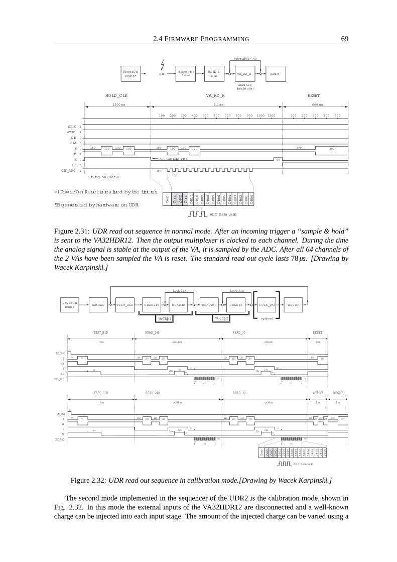
2.4 FIRMWARE PROGRAMMING 69
DB1
1
DB10
DB09
DB08
DB07
DB06
DB05
DB04
DB03
DB02
DB01
DB00
Zero
Zero
Zero
Zero
ADC Data valid
Peaking Tim e2,4 ms
Power O nReset *
HO LD &CLK
RESET
Repetitions = 63
VA_RD_R
Read ADC(Real M ode)
Tim ing: VaRDet50
HIT
VA_RD_R
90
150
50
RESET
S
SB
H
HB
CLK_ADC
0
0
1
0
0
SCLK
/SYNC
DIN
1
1
CAL
1
0
HO LD_CLK
150 100 100 100 150 100 100 100 300 300
100 200 300 400 500 600 700 800 900 1000 1100 100 200 300 400 500
1200 ns 1.2 ms 600 ns
ADC Sam pling Tim e
*) Power O n Reset is realized by the first run
SB generated by hardware on UDR
Figure 2.31: UDR read out sequence in normal mode. After an incoming trigger a “sample & hold”is sent to the VA32HDR12. Then the output multiplexer is clocked to each channel. During the timethe analog signal is stable at the output of the VA, it is sampled by the ADC. After all 64 channels ofthe 2 VAs have been sampled the VA is reset. The standard read out cycle lasts 78µs. [Drawing byWacek Karpinski.]
DB11
DB10
DB09
DB08
DB07
DB06
DB05
DB04
DB03
DB02
DB01
DB00
Zero
Zero
Zero
Zero
ADC Data valid
SetDAC TEST_HLD READ240PowerOnReset
READ30 RESET(+CLK_VA)
S
SB
H
HB
CLK_ADC
Trg_Test
1
TEST_HLD READ_240
2 ms
1
1
10
1
50
300300
400
250
240u
250250
2,4u60
125
100
77550
250
READ_30
250
30u
250250
2,4u60
125
100
77550
250 500500
1 ms
RESET
ca.244 ms ca.34 ms
S
SB
H
HB
CLK_ADC
Trg_Test
1
TEST_HLD READ_240
2 ms
1
1
10
1
50
300300
400
250
240u
250250
2,4u60
125
100
77550
250
READ_30
250
30u
250250
2,4u60
125
100
77550
250 250250
1 ms
+Clk_VA
ca.244 ms ca.34 ms
500500
1 ms
RESET
250 250
Loop 31x
READ240 READ30
Loop 31x
optionalVA-Chip 1 VA-Chip 2
Figure 2.32: UDR read out sequence in calibration mode.[Drawing by Wacek Karpinski.]
The second mode implemented in the sequencer of the UDR2 is the calibration mode, shown inFig. 2.32. In this mode the external inputs of the VA32HDR12 are disconnected and a well-knowncharge can be injected into each input stage. The amount of the injected charge can be varied using a
70 SPACE-GRADE ELECTRONICS FOR THE AMS02 DETECTOR
DAC on the UFE which is connected via a capacitor to the calibration input of the VA32HDR12.
A second feature of this mode is the variable delay between sample & hold and the clocking ofthe multiplexer. This allows to check if the internal timing of the VA32HDR12 has changed due toexternal effects like temperature and radiation damage.
This sequence is much more complicated than the normal read out, as the VA32HDR12 can onlyconnect one input stage at a time to the external calibration pulse and needs to be reset before the nextchannel can be calibrated. Thus the calibration procedure is the following:
First the DAC is set to the desired value. As the setup time of the DAC is not negligible, one hasto wait at least 5ms before starting the calibration sequence of the VA32HDR12.
In the beginning of the calibration sequence the VA32HDR12 is set to the test pulse mode. Aftera short hold time the input multiplexer is clocked to the desired channel. A short preparation time isrequired before the test pulse can be generated. An adjustable delay (0 to 6.3µs) allows to sample theoutput of the shaper and select the optimal timing for the normal read out. After reading out a channelin the calibration mode a long delay (20µs) is required before the chip can be reset and the calibrationsequence for the next channel can be started.
First measurement results
In order to verify the proper behaviour of the VA32HDR12 when using a specific sequence, extensivestudies were done. These studies include e.g. pedestal taking, timing and linearity scans. Furthermore,long-term tests were performed. In the following part some of the results from these tests will bepresented.
The first test with a new sequence is always to read a sufficient number of cycles and calculatethe pedestals and their noise distribution. Some of the problematic features of the VA32HDR12 canbe already observed in this measurement. For example, a problem with the first channel of a UFEwas noticed, when using the same timing for all channels. The obvious solution was to use a slightlylonger hold time (1200ns) for the first channel and standard timing (600ns) for all the others.
Both with the normal read out mode and with the calibration mode a timing scan can be performed.While this requires for the normal read out mode a special method for injecting charge into the inputsof the VA32HDR12 and an external adjustable delay unit, the calibration mode allows to do thiswithout external hardware.
For this timing scan a constant signal is applied to the inputs of the VA32HDR12 and the timebetween the trigger and the read out is varied. The expected peaking time of the VA32HDR12 is 2.4µs[IDE00]. In the calibration sequence the delay can be chosen from 0 to 6.3µs in steps of 100ns. Ameasurement performed using the S9007 setup is shown in Fig. 2.33.
A second feature of the calibration mode is the possibility to scan the input range of the VA32HDR12with a test pulse and thus check the linearity of the VA32HDR12 and the ADC. The result of a mea-surement performed with the S9007 is shown in Fig. 2.34. It can be clearly seen that the VA32HDR12has a linear range till ∼ 3000 ADC counts. After this a slight deviation from the linear behaviour canbe observed. This non-linearity is caused by the starting of the saturation of the VA32HDR12. Thecut-off of the input range at 4096 ADC counts is caused by the upper limit of the input range of the12bit ADC.
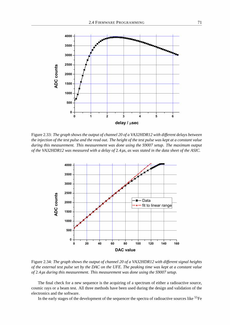
2.4 FIRMWARE PROGRAMMING 71
Figure 2.33: The graph shows the output of channel 20 of a VA32HDR12 with different delays betweenthe injection of the test pulse and the read out. The height of the test pulse was kept at a constant valueduring this measurement. This measurement was done using the S9007 setup. The maximum outputof the VA32HDR12 was measured with a delay of 2.4µs, as was stated in the data sheet of the ASIC.
Figure 2.34: The graph shows the output of channel 20 of a VA32HDR12 with different signal heightsof the external test pulse set by the DAC on the UFE. The peaking time was kept at a constant valueof 2.4µs during this measurement. This measurement was done using the S9007 setup.
The final check for a new sequence is the acquiring of a spectrum of either a radioactive source,cosmic rays or a beam test. All three methods have been used during the design and validation of theelectronics and the software.
In the early stages of the development of the sequencer the spectra of radioactive sources like 55Fe
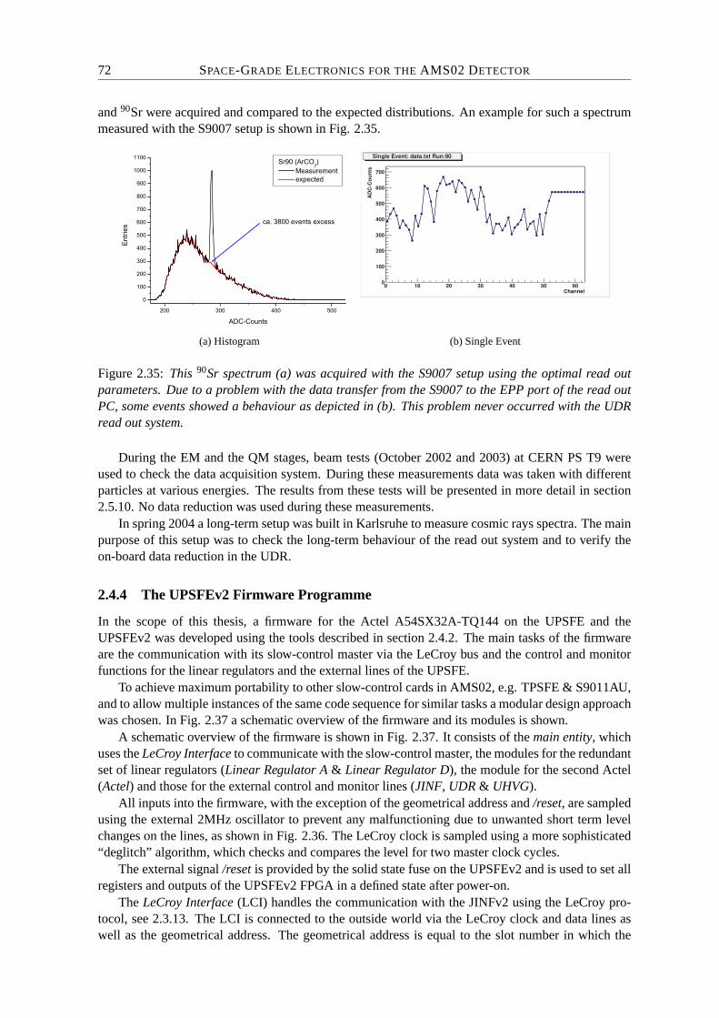
72 SPACE-GRADE ELECTRONICS FOR THE AMS02 DETECTOR
and 90Sr were acquired and compared to the expected distributions. An example for such a spectrummeasured with the S9007 setup is shown in Fig. 2.35.
(a) Histogram (b) Single Event
Figure 2.35: This 90Sr spectrum (a) was acquired with the S9007 setup using the optimal read outparameters. Due to a problem with the data transfer from the S9007 to the EPP port of the read outPC, some events showed a behaviour as depicted in (b). This problem never occurred with the UDRread out system.
During the EM and the QM stages, beam tests (October 2002 and 2003) at CERN PS T9 wereused to check the data acquisition system. During these measurements data was taken with differentparticles at various energies. The results from these tests will be presented in more detail in section2.5.10. No data reduction was used during these measurements.
In spring 2004 a long-term setup was built in Karlsruhe to measure cosmic rays spectra. The mainpurpose of this setup was to check the long-term behaviour of the read out system and to verify theon-board data reduction in the UDR.
2.4.4 The UPSFEv2 Firmware Programme
In the scope of this thesis, a firmware for the Actel A54SX32A-TQ144 on the UPSFE and theUPSFEv2 was developed using the tools described in section 2.4.2. The main tasks of the firmwareare the communication with its slow-control master via the LeCroy bus and the control and monitorfunctions for the linear regulators and the external lines of the UPSFE.
To achieve maximum portability to other slow-control cards in AMS02, e.g. TPSFE & S9011AU,and to allow multiple instances of the same code sequence for similar tasks a modular design approachwas chosen. In Fig. 2.37 a schematic overview of the firmware and its modules is shown.
A schematic overview of the firmware is shown in Fig. 2.37. It consists of the main entity, whichuses the LeCroy Interface to communicate with the slow-control master, the modules for the redundantset of linear regulators (Linear Regulator A & Linear Regulator D), the module for the second Actel(Actel) and those for the external control and monitor lines (JINF, UDR & UHVG).
All inputs into the firmware, with the exception of the geometrical address and /reset, are sampledusing the external 2MHz oscillator to prevent any malfunctioning due to unwanted short term levelchanges on the lines, as shown in Fig. 2.36. The LeCroy clock is sampled using a more sophisticated“deglitch” algorithm, which checks and compares the level for two master clock cycles.
The external signal /reset is provided by the solid state fuse on the UPSFEv2 and is used to set allregisters and outputs of the UPSFEv2 FPGA in a defined state after power-on.
The LeCroy Interface (LCI) handles the communication with the JINFv2 using the LeCroy pro-tocol, see 2.3.13. The LCI is connected to the outside world via the LeCroy clock and data lines aswell as the geometrical address. The geometrical address is equal to the slot number in which the
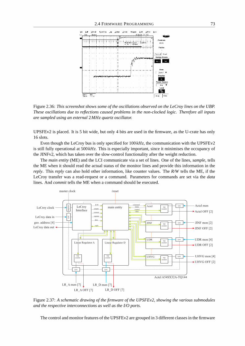
2.4 FIRMWARE PROGRAMMING 73
Figure 2.36: This screenshot shows some of the oscillations observed on the LeCroy lines on the UBP.These oscillations due to reflections caused problems in the non-clocked logic. Therefore all inputsare sampled using an external 2MHz quartz oscillator.
UPSFEv2 is placed. It is 5 bit wide, but only 4 bits are used in the firmware, as the U-crate has only16 slots.
Even though the LeCroy bus is only specified for 100kHz, the communication with the UPSFEv2is still fully operational at 500kHz. This is especially important, since it minimises the occupancy ofthe JINFv2, which has taken over the slow-control functionality after the weight reduction.
The main entity (ME) and the LCI communicate via a set of lines. One of the lines, sample, tellsthe ME when it should read the actual status of the monitor lines and provide this information in thereply. This reply can also hold other information, like counter values. The R/W tells the ME, if theLeCroy transfer was a read-request or a command. Parameters for commands are set via the datalines. And commit tells the ME when a command should be executed.
LeCroy clock
LeCroy data in
deg
litc
hsy
nc
sync sync
sync
sync
sync
sync
geo. address [4]
LeCroy data out
master clock
LeCroyInterface
main entity Actel
JINF
UDR
UHVG
R/W
sample
commit
register
data
reply
command
status
value
tripcounter
tripcounter
tripcounter
tripcounter
tripcounter
tripcounter
/reset
control
Actel mon
Actel OFF [2]
JINF mon [2]
UDR mon [4]
UHVG mon [4]
JINF OFF [2]
UDR OFF [2]
UHVG OFF [2]
LR_A mon [7]
LR_A OFF [7]
LR_D mon [7]
LR_D OFF [7]
Linear Regulator A Linear Regulator D
Actel A54SX32A-TQ144
Figure 2.37: A schematic drawing of the firmware of the UPSFEv2, showing the various submodulesand the respective interconnections as well as the I/O ports.
The control and monitor features of the UPSFEv2 are grouped in 3 different classes in the firmware
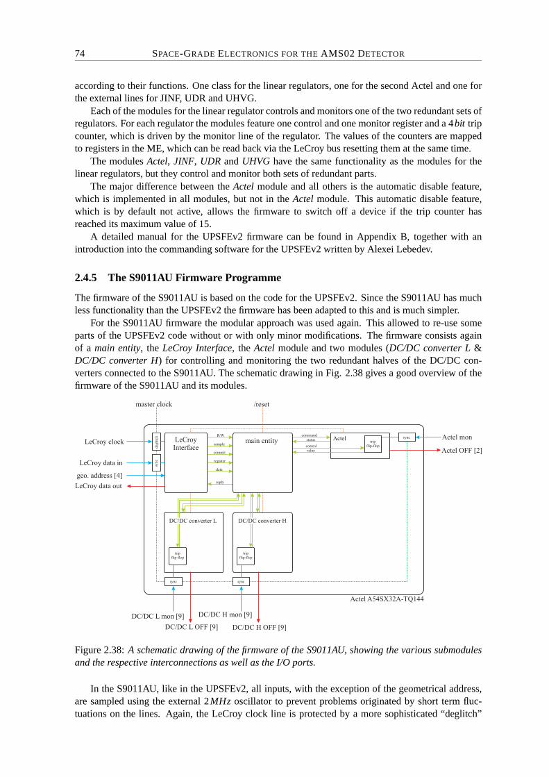
74 SPACE-GRADE ELECTRONICS FOR THE AMS02 DETECTOR
according to their functions. One class for the linear regulators, one for the second Actel and one forthe external lines for JINF, UDR and UHVG.
Each of the modules for the linear regulator controls and monitors one of the two redundant sets ofregulators. For each regulator the modules feature one control and one monitor register and a 4bit tripcounter, which is driven by the monitor line of the regulator. The values of the counters are mappedto registers in the ME, which can be read back via the LeCroy bus resetting them at the same time.
The modules Actel, JINF, UDR and UHVG have the same functionality as the modules for thelinear regulators, but they control and monitor both sets of redundant parts.
The major difference between the Actel module and all others is the automatic disable feature,which is implemented in all modules, but not in the Actel module. This automatic disable feature,which is by default not active, allows the firmware to switch off a device if the trip counter hasreached its maximum value of 15.
A detailed manual for the UPSFEv2 firmware can be found in Appendix B, together with anintroduction into the commanding software for the UPSFEv2 written by Alexei Lebedev.
2.4.5 The S9011AU Firmware Programme
The firmware of the S9011AU is based on the code for the UPSFEv2. Since the S9011AU has muchless functionality than the UPSFEv2 the firmware has been adapted to this and is much simpler.
For the S9011AU firmware the modular approach was used again. This allowed to re-use someparts of the UPSFEv2 code without or with only minor modifications. The firmware consists againof a main entity, the LeCroy Interface, the Actel module and two modules (DC/DC converter L &DC/DC converter H) for controlling and monitoring the two redundant halves of the DC/DC con-verters connected to the S9011AU. The schematic drawing in Fig. 2.38 gives a good overview of thefirmware of the S9011AU and its modules.
LeCroy clock
LeCroy data in
deg
litc
hsy
nc
sync sync
sync
geo. address [4]
LeCroy data out
master clock
LeCroyInterface
main entity ActelR/W
sample
commit
register
data
reply
command
status
value
tripflip-flop
tripflip-flop
/reset
control
Actel mon
Actel OFF [2]
DC/DC L mon [9]
DC/DC L OFF [9]
DC/DC H mon [9]
DC/DC H OFF [9]
DC/DC converter L
Actel A54SX32A-TQ144
tripflip-flop
DC/DC converter H
Figure 2.38: A schematic drawing of the firmware of the S9011AU, showing the various submodulesand the respective interconnections as well as the I/O ports.
In the S9011AU, like in the UPSFEv2, all inputs, with the exception of the geometrical address,are sampled using the external 2MHz oscillator to prevent problems originated by short term fluc-tuations on the lines. Again, the LeCroy clock line is protected by a more sophisticated “deglitch”

2.5 PRODUCTION AND QUALIFICATION 75
module, as this line drives most of the logic in the FPGA.As the main entity and the LeCroy Interface are almost identical to the code of the UPSFEv2, they
use the same links for data exchange and synchronisation. In principle a second LeCroy Interface isforeseen for each FPGA on the PCB of the S9011AU, but this option is not used, as there are no freeLeCroy links available in the U-crate. The second LeCroy link would also require additional logic toprevent malfunctioning if both links are active at the same time.
Like for the UPSFEv2 the LeCroy clock frequency for the communication with the S9011AU canbe operated at up to 500kHz, exceeding the specifications by a factor of 5.
Unlike in the UPSFEv2 there are no trip counters in the S9011AU firmware. In the occurrence ofa trip of either a DC/DC converter or the solid-state fuse of the other Actel a flip-flop is set. The statusof these flip-flops can be read back via the LeCroy link, which also resets the flip-flops.
Together with a short description of the commanding software for the S9011AU, written by AlexeiLebedev, a detailed manual for the S9011AU can be found in Appendix C.
2.5 Production and Qualification
2.5.1 Design Process & Production Procedures
The design process of the electronics for the AMS02 experiment is divided into four parts. The firststage is the prototyping. After this an engineering model is built, before the qualification model isproduced. The final product flown into space is the flight model.
In the following paragraphs this design process will be described with the help of the example ofthe data reduction board (UDR) for the TRD.
Prototyping
The first stage of the design flow is the prototyping phase. In this phase the principle design is chosenand a first version of the board, often a multi-purpose board, is built.
In the case of the data reduction boards this prototype board was the S9007. It consists of thesame core components as the final device, namely a DSP, an FPGA and a memory chip. All detectorspecific components were connected to the S9007 as piggy-back PCBs. A picture of this board isshown in Fig. 2.30(b).
With this prototype a set of functional tests is performed in order to verify that the performance ofthe design is within the requirements.
Engineering Modules - EM
The next stage of the design process is the engineering phase. In this stage the PCB design is asclose as possible to the final design. The main difference to the following stages is the usage ofnon-space-qualified components on the PCBs.
With these Engineering Modules (EM) a first integration test is performed to verify the systemdesign. In the example of the UDR, these boards were also used during a beam test, see section2.5.10, to check the performance of the detector modules and the front-end hybrids.
Qualification Modules - QM
The qualification stage is one of the most important phases of the design process of space-gradeelectronics. This is the first time an electronics module is built exactly the way it will be flown duringthe mission.
The PCB design is frozen before the Qualification Module (QM) production. Only minor changesare allowed from QM to the final production. The qualification modules are submitted to the fullspectrum of tests to verify the design of the individual board.
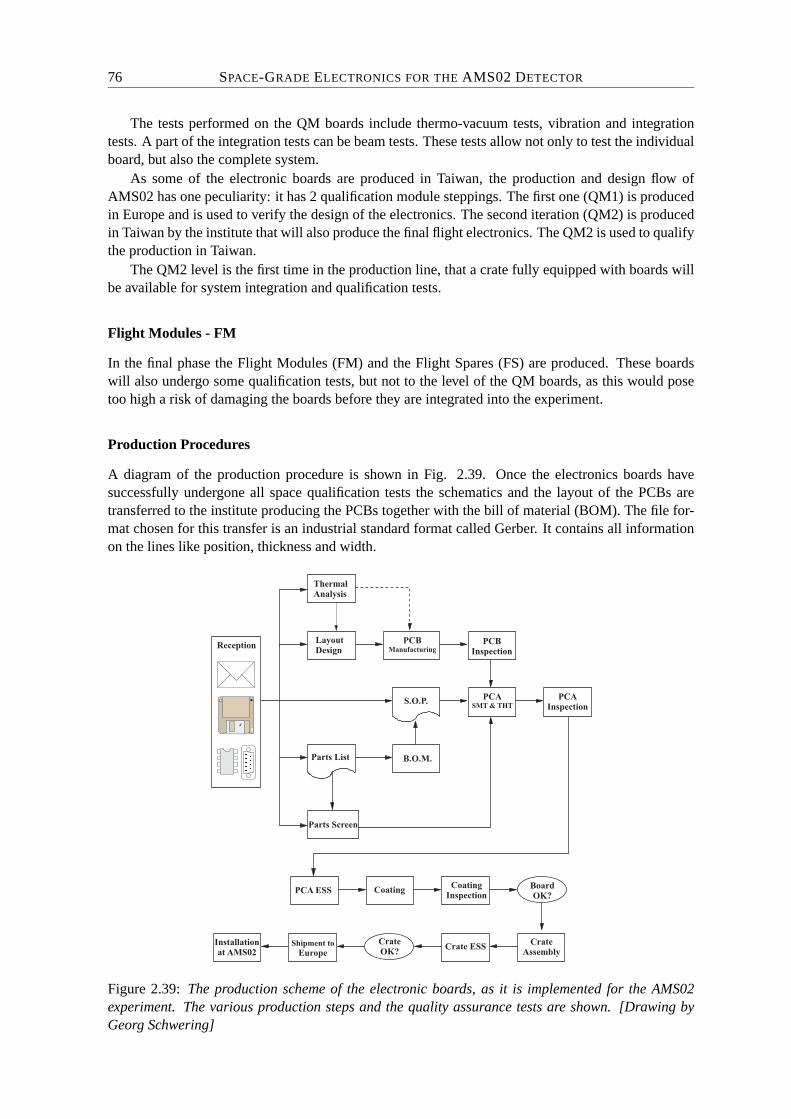
76 SPACE-GRADE ELECTRONICS FOR THE AMS02 DETECTOR
The tests performed on the QM boards include thermo-vacuum tests, vibration and integrationtests. A part of the integration tests can be beam tests. These tests allow not only to test the individualboard, but also the complete system.
As some of the electronic boards are produced in Taiwan, the production and design flow ofAMS02 has one peculiarity: it has 2 qualification module steppings. The first one (QM1) is producedin Europe and is used to verify the design of the electronics. The second iteration (QM2) is producedin Taiwan by the institute that will also produce the final flight electronics. The QM2 is used to qualifythe production in Taiwan.
The QM2 level is the first time in the production line, that a crate fully equipped with boards willbe available for system integration and qualification tests.
Flight Modules - FM
In the final phase the Flight Modules (FM) and the Flight Spares (FS) are produced. These boardswill also undergo some qualification tests, but not to the level of the QM boards, as this would posetoo high a risk of damaging the boards before they are integrated into the experiment.
Production Procedures
A diagram of the production procedure is shown in Fig. 2.39. Once the electronics boards havesuccessfully undergone all space qualification tests the schematics and the layout of the PCBs aretransferred to the institute producing the PCBs together with the bill of material (BOM). The file for-mat chosen for this transfer is an industrial standard format called Gerber. It contains all informationon the lines like position, thickness and width.
Reception
ThermalAnalysis
LayoutDesign
PCBManufacturing
PCBInspection
PCASMT & THT
S.O.P.
Parts List B.O.M.
PCAInspection
Parts Screen
PCA ESS CoatingCoating
InspectionBoardOK?
CrateAssembly
Crate ESSCrateOK?
Shipment to
Europe
Installationat AMS02
Figure 2.39: The production scheme of the electronic boards, as it is implemented for the AMS02experiment. The various production steps and the quality assurance tests are shown. [Drawing byGeorg Schwering]

2.5 PRODUCTION AND QUALIFICATION 77
As all PCBs used in AMS02 are of multi-layer type, the PCBs are produced by manufacturingall layers separately and laminating them together. Each layer is optically inspected after production.The complete stack of the layers is then checked after the laminating using X-ray systems. Once theboards have passed this test, vias are drilled and the contacts are grown.
When the naked board is completed, the assembly of the board (PCA) starts. All components usedare either space-grade or they are specially screened before the PCA.
The fully assembled board then has to pass a functional test to verify that it is fully operational.After this test the board is coated. The next step in the production is the environmental stress screening(ESS). During this test, the temperature of the board is varied from the minimum non-operational tothe minimum operational on to the maximum operational and finally to the maximum non-operationaltemperature. This cycle is done a few times. After the ESS the boards have to pass a second func-tional test to verify they still work within the specifications. Finally the boards are put into a climatecontrolled clean storage, where they are kept till the assembly of the detector.
2.5.2 Space Qualification Procedure
All electronics boards must undergo a qualification procedure after their production. These tests canbe classified into two groups: the single board level test and the crate level tests.
Single Board Level Tests
The single board level tests are done directly after the production of the electronics boards, as shownin Fig. 2.40. The first step of the testing is an inspection of the boards by the Chung-Shan Institute ofScience and Technology (CSIST) using visible light and X-rays.
1. Production line CSIST 2. Inspection CSIST 3. Functional test AMS
0 Co 0 C
o
-40 C
+95 Co
o10x
4. Coating CSIST 5. Thermal Cycling CSIST 6. Functional test AMS
Figure 2.40: The qualification scheme, on single board level, implemented by AMS for the electronicsproduction at CSIST. [based on a drawing by Georg Schwering]
The second stage is a functional test of the board. Depending on the type of board this step requiresquite a lot of additional equipment, e.g. a test backplane as it is described later on in this section.
During these functional tests all features of the various cards must be tested. For the UPSFEv2,for example, this means testing the communication with the FPGA, all linear regulators on the boardand all external control and feed-back lines.
If the boards pass this first round of functional testing, they are protected by the application ofconformal coating. Afterwards they are put into a climate chamber and thermally cycled. After this
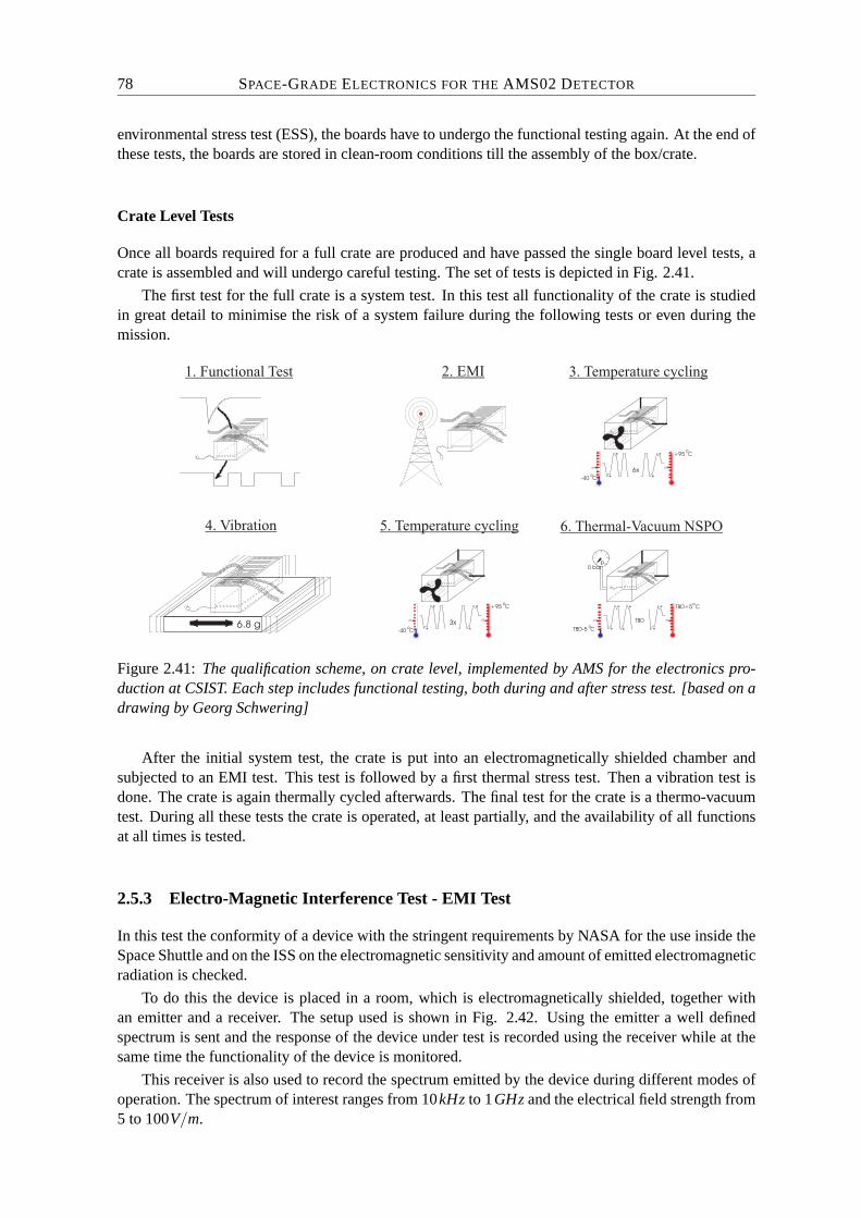
78 SPACE-GRADE ELECTRONICS FOR THE AMS02 DETECTOR
environmental stress test (ESS), the boards have to undergo the functional testing again. At the end ofthese tests, the boards are stored in clean-room conditions till the assembly of the box/crate.
Crate Level Tests
Once all boards required for a full crate are produced and have passed the single board level tests, acrate is assembled and will undergo careful testing. The set of tests is depicted in Fig. 2.41.
The first test for the full crate is a system test. In this test all functionality of the crate is studiedin great detail to minimise the risk of a system failure during the following tests or even during themission.
1. Functional Test 2. EMI
0 Co 0 C
o
*
*
*
*
6x-40 C
+95 Co
o
3. Temperature cycling
6.8 g
4. Vibration
0 Co 0 C
o
3x-40 C
+95 Co
o *
*
*
*
5. Temperature cycling 6. Thermal-Vacuum NSPO
TBD0 Co 0 C
o
*
*
*
*
0 barp
TBD+5 C
TBD-5 Co
o
*
*
Figure 2.41: The qualification scheme, on crate level, implemented by AMS for the electronics pro-duction at CSIST. Each step includes functional testing, both during and after stress test. [based on adrawing by Georg Schwering]
After the initial system test, the crate is put into an electromagnetically shielded chamber andsubjected to an EMI test. This test is followed by a first thermal stress test. Then a vibration test isdone. The crate is again thermally cycled afterwards. The final test for the crate is a thermo-vacuumtest. During all these tests the crate is operated, at least partially, and the availability of all functionsat all times is tested.
2.5.3 Electro-Magnetic Interference Test - EMI Test
In this test the conformity of a device with the stringent requirements by NASA for the use inside theSpace Shuttle and on the ISS on the electromagnetic sensitivity and amount of emitted electromagneticradiation is checked.
To do this the device is placed in a room, which is electromagnetically shielded, together withan emitter and a receiver. The setup used is shown in Fig. 2.42. Using the emitter a well definedspectrum is sent and the response of the device under test is recorded using the receiver while at thesame time the functionality of the device is monitored.
This receiver is also used to record the spectrum emitted by the device during different modes ofoperation. The spectrum of interest ranges from 10kHz to 1GHz and the electrical field strength from5 to 100V/m.
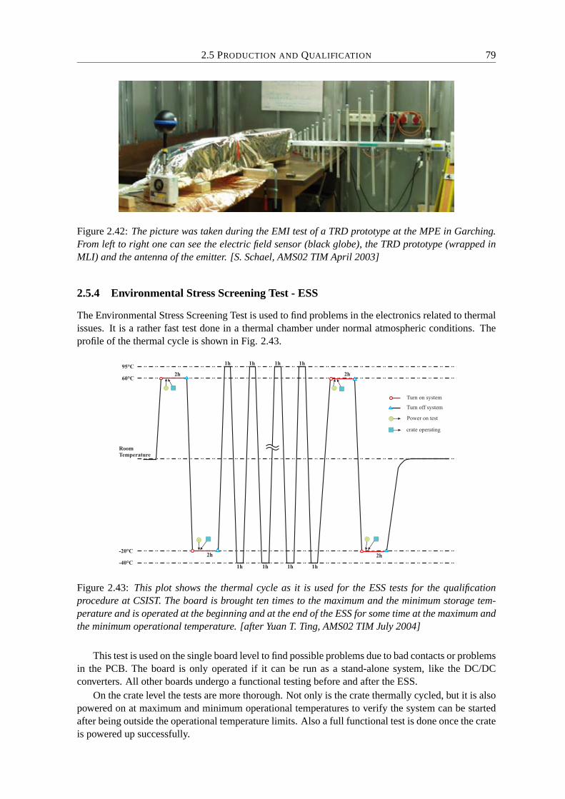
2.5 PRODUCTION AND QUALIFICATION 79
Figure 2.42: The picture was taken during the EMI test of a TRD prototype at the MPE in Garching.From left to right one can see the electric field sensor (black globe), the TRD prototype (wrapped inMLI) and the antenna of the emitter. [S. Schael, AMS02 TIM April 2003]
2.5.4 Environmental Stress Screening Test - ESS
The Environmental Stress Screening Test is used to find problems in the electronics related to thermalissues. It is a rather fast test done in a thermal chamber under normal atmospheric conditions. Theprofile of the thermal cycle is shown in Fig. 2.43.
95°C
60°C
-20°C
-40°C
RoomTemperature
Turn on system
Turn off system
Power on test
crate operating
1h 1h 1h 1h
2h2h
2h
1h 1h 1h 1h
2h
Figure 2.43: This plot shows the thermal cycle as it is used for the ESS tests for the qualificationprocedure at CSIST. The board is brought ten times to the maximum and the minimum storage tem-perature and is operated at the beginning and at the end of the ESS for some time at the maximum andthe minimum operational temperature. [after Yuan T. Ting, AMS02 TIM July 2004]
This test is used on the single board level to find possible problems due to bad contacts or problemsin the PCB. The board is only operated if it can be run as a stand-alone system, like the DC/DCconverters. All other boards undergo a functional testing before and after the ESS.
On the crate level the tests are more thorough. Not only is the crate thermally cycled, but it is alsopowered on at maximum and minimum operational temperatures to verify the system can be startedafter being outside the operational temperature limits. Also a full functional test is done once the crateis powered up successfully.
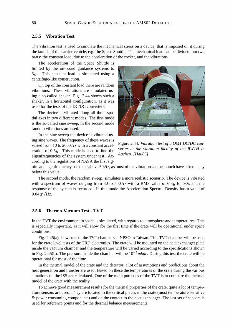
80 SPACE-GRADE ELECTRONICS FOR THE AMS02 DETECTOR
2.5.5 Vibration Test
The vibration test is used to simulate the mechanical stress on a device, that is imposed on it duringthe launch of the carrier vehicle, e.g. the Space Shuttle. The mechanical load can be divided into twoparts: the constant load, due to the acceleration of the rocket, and the vibrations.
Figure 2.44: Vibration test of a QM1 DC/DC con-verter at the vibration facility of the RWTH inAachen. [Hau05]
The acceleration of the Space Shuttle islimited by the on-board guidance systems to3g. This constant load is simulated using acentrifuge-like construction.
On top of the constant load there are randomvibrations. These vibrations are simulated us-ing a so-called shaker. Fig. 2.44 shows such ashaker, in a horizontal configuration, as it wasused for the tests of the DC/DC converters.
The device is vibrated along all three spa-tial axes in two different modes. The first modeis the so-called sine sweep, in the second moderandom vibrations are used.
In the sine sweep the device is vibrated us-ing sine waves. The frequency of these waves isvaried from 10 to 2000Hz with a constant accel-eration of 0.5g. This mode is used to find theeigenfrequencies of the system under test. Ac-cording to the regulations of NASA the first sig-nificant eigenfrequency has to be above 50Hz, as most of the vibrations at the launch have a frequencybelow this value.
The second mode, the random sweep, simulates a more realistic scenario. The device is vibratedwith a spectrum of waves ranging from 80 to 500Hz with a RMS value of 6.8g for 90s and theresponse of the system is recorded. In this mode the Acceleration Spectral Density has a value of0.04g2/Hz.
2.5.6 Thermo-Vacuum Test - TVT
In the TVT the environment in space is simulated, with regards to atmosphere and temperatures. Thisis especially important, as it will show for the first time if the crate will be operational under spaceconditions.
Fig. 2.45(a) shows one of the TVT chambers at NPSO in Taiwan. This TVT chamber will be usedfor the crate level tests of the TRD electronics. The crate will be mounted on the heat exchanger plateinside the vacuum chamber and the temperature will be varied according to the specifications shownin Fig. 2.45(b). The pressure inside the chamber will be 10−5 mbar. During this test the crate will beoperational for most of the time.
In the thermal model of the crate and the detector, a lot of assumptions and predictions about theheat generation and transfer are used. Based on these the temperatures of the crate during the varioussituations on the ISS are calculated. One of the main purposes of the TVT is to compare the thermalmodel of the crate with the reality.
To achieve good measurement results for the thermal properties of the crate, quite a lot of temper-ature sensors are used. They are located in the critical places in the crate (most temperature sensitive& power consuming components) and on the contact to the heat exchanger. The last set of sensors isused for reference points and for the thermal balance measurements.
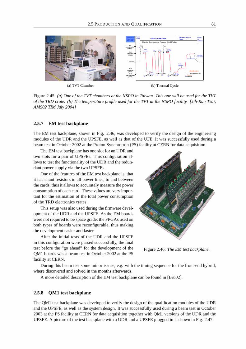
2.5 PRODUCTION AND QUALIFICATION 81
(a) TVT Chamber
Thermal Balance Phase
PumpDown
Chamber Environments: Pressure1.0x10-5 mbar
ReturnToAmbient
Ambient
Hotnon-operation
(+85oC)
Temperature(Proto-flightTest Level)
Thermal Cycling Phase
HotOperation(+55oC)
Coldnon-operation
(-45oC)
ColdOperation
(-25oC)
2 hrsHot soak
Hot Balance
Cold Balance
TransientCool-Down
1 hr
1 hr 1 hr
1hr
1 hr
Operation (on)
Non-operation (off)1 hr 1
hr Turn offTurn on
2 hrsHot soak
2 hrscold soak
2 hrscold soak
(b) Thermal Cycle
Figure 2.45: (a) One of the TVT chambers at the NSPO in Taiwan. This one will be used for the TVTof the TRD crate. (b) The temperature profile used for the TVT at the NSPO facility. [Jih-Run Tsai,AMS02 TIM July 2004]
2.5.7 EM test backplane
The EM test backplane, shown in Fig. 2.46, was developed to verify the design of the engineeringmodules of the UDR and the UPSFE, as well as that of the UFE. It was successfully used during abeam test in October 2002 at the Proton Synchrotron (PS) facility at CERN for data acquisition.
Figure 2.46: The EM test backplane.
The EM test backplane has one slot for an UDR andtwo slots for a pair of UPSFEs. This configuration al-lows to test the functionality of the UDR and the redun-dant power supply via the two UPSFEs.
One of the features of the EM test backplane is, thatit has shunt resistors in all power lines, to and betweenthe cards, thus it allows to accurately measure the powerconsumption of each card. These values are very impor-tant for the estimation of the total power consumptionof the TRD electronics crates.
This setup was also used during the firmware devel-opment of the UDR and the UPSFE. As the EM boardswere not required to be space grade, the FPGAs used onboth types of boards were reconfigurable, thus makingthe development easier and faster.
After the initial tests of the UDR and the UPSFEin this configuration were passed successfully, the finaltest before the “go ahead” for the development of theQM1 boards was a beam test in October 2002 at the PSfacility at CERN.
During this beam test some minor issues, e.g. with the timing sequence for the front-end hybrid,where discovered and solved in the months afterwards.
A more detailed description of the EM test backplane can be found in [Bru02].
2.5.8 QM1 test backplane
The QM1 test backplane was developed to verify the design of the qualification modules of the UDRand the UPSFE, as well as the system design. It was successfully used during a beam test in October2003 at the PS facility at CERN for data acquisition together with QM1 versions of the UDR and theUPSFE. A picture of the test backplane with a UDR and a UPSFE plugged in is shown in Fig. 2.47.
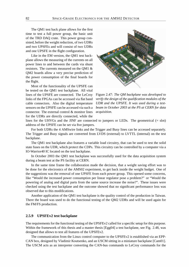
82 SPACE-GRADE ELECTRONICS FOR THE AMS02 DETECTOR
Figure 2.47: The QM backplane was developed toverify the design of the qualification modules of theUDR and the UPSFE. It was used during a test-beam in October 2003 at the PS at CERN for dataacquisition.
The QM1 test back plane allows for the firsttime to test a full power group, the basic unitof the TRD DAQ crate. This power group con-sisted, before the weight reduction, of two UDRsand two UPSFEs and will consist of two UDRsand one UPSFE in the flight configuration.
Like in the EM version, the QM1 test back-plane allows the measuring of the currents on allpower lines to and between the cards via shuntresistors. The currents measured on the QM1 &QM2 boards allow a very precise prediction ofthe power consumption of the final boards forthe flight.
Most of the functionality of the UPSFE canbe tested on the QM1 test backplane. All vitallines of the UPSFE are connected. The LeCroylinks of the FPGAs can be accessed via flat bandcable connectors. Also the digital temperaturesensors on the UPSFE can be accessed via such aconnector. The external control & monitor linesfor the UDRs are directly connected, while thelines for the UHVGs and the JINF are connected to jumpers or LEDs. The geometrical (= slot)address of the UPSFE can be set via five jumpers.
For both UDRs the 4 AMSwire links and the Trigger and Busy lines can be accessed separately.The Trigger and Busy signals are converted from LVDS (external) to LVTTL (internal) on the testbackplane.
The QM1 test backplane also features a variable load circuitry, that can be used to test the solidstate fuses on the UDR, which protect the CDPs. This circuitry can be controlled by a computer via aIO-Warrior40 IC located on the test backplane.
In October 2003 the QM1 test backplane was successfully used for the data acquisition systemduring a beam test at the PS facility at CERN.
In the same time frame the collaboration made the decision, that a weight saving effort was tobe done for the electronics of the AMS02 experiment, to get back inside the weight budget. One ofthe suggestions was the removal of one UPSFE from each power group. This opened some concerns,like “Would the increased power consumption per linear regulator pose a problem?” or “Would thepowering of analog and digital parts from the same source increase the noise?”. These issues werechecked using the test backplane and the outcome showed that no significant performance loss wasobserved due to this modifications.
Another application of the QM1 test backplane is the quality control of the production in Taiwan.There the board was used to do the functional testing of the QM2 UDRs and will be used again forthe FM/FS production.
2.5.9 UPSFEv2 test backplane
The requirements for the functional testing of the UPSFEv2 called for a specific setup for this purpose.Within the framework of this thesis and a master thesis [Egg04] a test backplane, see Fig. 2.48, wasdesigned that allows to test all features of the UPSFEv2.
The communication from the Linux control computer to the UPSFEv2 is established via an EPP-CAN box, designed by Vladimir Koutsenko, and an USCM sitting in a miniature backplane [Cam01].The USCM acts as an interpreter converting the CAN-bus commands to LeCroy commands for the
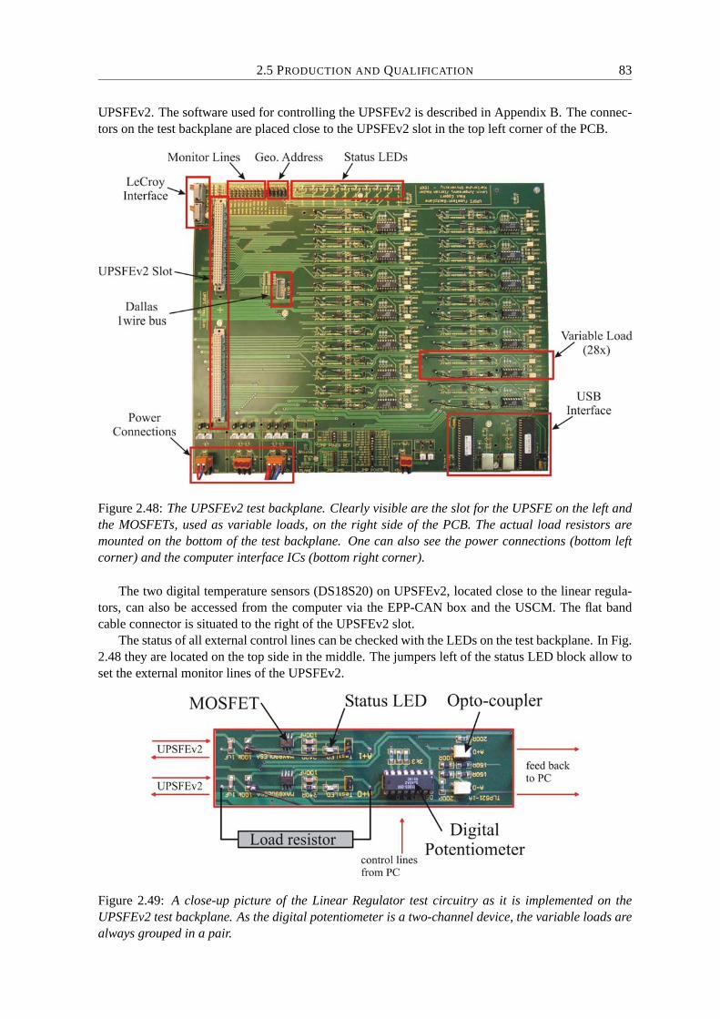
2.5 PRODUCTION AND QUALIFICATION 83
UPSFEv2. The software used for controlling the UPSFEv2 is described in Appendix B. The connec-tors on the test backplane are placed close to the UPSFEv2 slot in the top left corner of the PCB.
Figure 2.48: The UPSFEv2 test backplane. Clearly visible are the slot for the UPSFE on the left andthe MOSFETs, used as variable loads, on the right side of the PCB. The actual load resistors aremounted on the bottom of the test backplane. One can also see the power connections (bottom leftcorner) and the computer interface ICs (bottom right corner).
The two digital temperature sensors (DS18S20) on UPSFEv2, located close to the linear regula-tors, can also be accessed from the computer via the EPP-CAN box and the USCM. The flat bandcable connector is situated to the right of the UPSFEv2 slot.
The status of all external control lines can be checked with the LEDs on the test backplane. In Fig.2.48 they are located on the top side in the middle. The jumpers left of the status LED block allow toset the external monitor lines of the UPSFEv2.
Figure 2.49: A close-up picture of the Linear Regulator test circuitry as it is implemented on theUPSFEv2 test backplane. As the digital potentiometer is a two-channel device, the variable loads arealways grouped in a pair.

84 SPACE-GRADE ELECTRONICS FOR THE AMS02 DETECTOR
The most important function of the test backplane is the testing of the linear regulators on theUPSFEv2 and their self protection systems. For all 14 linear regulators the (+) and the (-) branch canbe tested independently. This is necessary because the over current protection of the linear regulatorsis implemented separately for the two branches. In total 28 test circuits are required.
Figure 2.50: A screen shot of the Soft-ware for controlling the UPSFE testbackplane.
Due to this high number of channels, which were caus-ing addressing problems on the control bus, it was decidedto organise load circuits on the test backplane in two com-pletely independent parts. Both parts, clearly visible in Fig.2.48, consist of seven 2-channel potentiometers each con-trolling two MOSFETs.
The design of the test circuitry, see Fig. 2.49, for thelinear regulators is based on an application note for anadjustable load using the MAX890L by Maxim [Dal00].This MOSFET IC can be controlled via an external poten-tiometer. In our case this was implemented using a digitalpotentiometer. This potentiometer can be interfaced to aµController using a 2-wire serial bus compatible with I2C,an industrial standard defined by Philips Semiconductors[Phi00].
The status of each channel, (+) and (-) of one linearregulator, is indicated by LEDs and can be read back intothe computer controlling the test backplane via opto-couplers and the µController. Fig. 2.50 shows ascreenshot of the LabView software on the PC.
Figure 2.51: The UPSFEv2 test setup, as it was used during the quality control of the QM2 productionat CSIST in Taiwan. The setup from left to right: The laptop computer was used to control theUSPFEv2 via an EPPCAN box and an USCM. The oscilloscope is needed for the measurement ofthe timing of the solid-state fuses and the linear regulators. Next is the UPSFEv2 itself, sitting in theUPSFEv2 test backplane. On its right are two power supplies, one for the digital part, one for theanalog part together with the digital multi-meter used for monitoring the currents. The computer usedto control the DMM and to log the data from it is located right next to it.
The two µControllers used on the test backplane are of the type IO-Warrior40 produced by CodeMercenaries. These µControllers have one USB link, and 32 IO pins. Due to the limitations of theUSB port the communication data word rate is ∼ 120Hz. Two of the IO pins can be used in a special
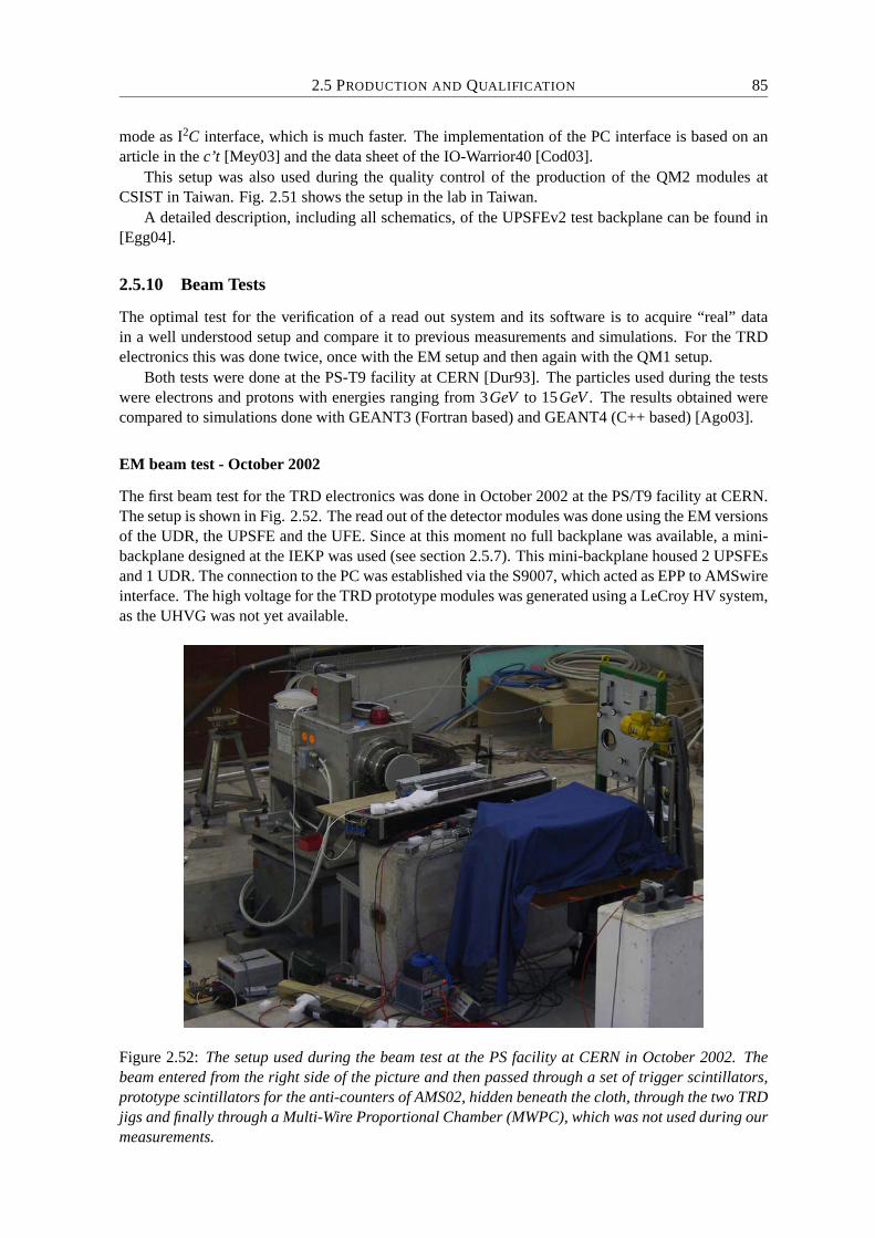
2.5 PRODUCTION AND QUALIFICATION 85
mode as I2C interface, which is much faster. The implementation of the PC interface is based on anarticle in the c’t [Mey03] and the data sheet of the IO-Warrior40 [Cod03].
This setup was also used during the quality control of the production of the QM2 modules atCSIST in Taiwan. Fig. 2.51 shows the setup in the lab in Taiwan.
A detailed description, including all schematics, of the UPSFEv2 test backplane can be found in[Egg04].
2.5.10 Beam Tests
The optimal test for the verification of a read out system and its software is to acquire “real” datain a well understood setup and compare it to previous measurements and simulations. For the TRDelectronics this was done twice, once with the EM setup and then again with the QM1 setup.
Both tests were done at the PS-T9 facility at CERN [Dur93]. The particles used during the testswere electrons and protons with energies ranging from 3GeV to 15GeV . The results obtained werecompared to simulations done with GEANT3 (Fortran based) and GEANT4 (C++ based) [Ago03].
EM beam test - October 2002
The first beam test for the TRD electronics was done in October 2002 at the PS/T9 facility at CERN.The setup is shown in Fig. 2.52. The read out of the detector modules was done using the EM versionsof the UDR, the UPSFE and the UFE. Since at this moment no full backplane was available, a mini-backplane designed at the IEKP was used (see section 2.5.7). This mini-backplane housed 2 UPSFEsand 1 UDR. The connection to the PC was established via the S9007, which acted as EPP to AMSwireinterface. The high voltage for the TRD prototype modules was generated using a LeCroy HV system,as the UHVG was not yet available.
Figure 2.52: The setup used during the beam test at the PS facility at CERN in October 2002. Thebeam entered from the right side of the picture and then passed through a set of trigger scintillators,prototype scintillators for the anti-counters of AMS02, hidden beneath the cloth, through the two TRDjigs and finally through a Multi-Wire Proportional Chamber (MWPC), which was not used during ourmeasurements.
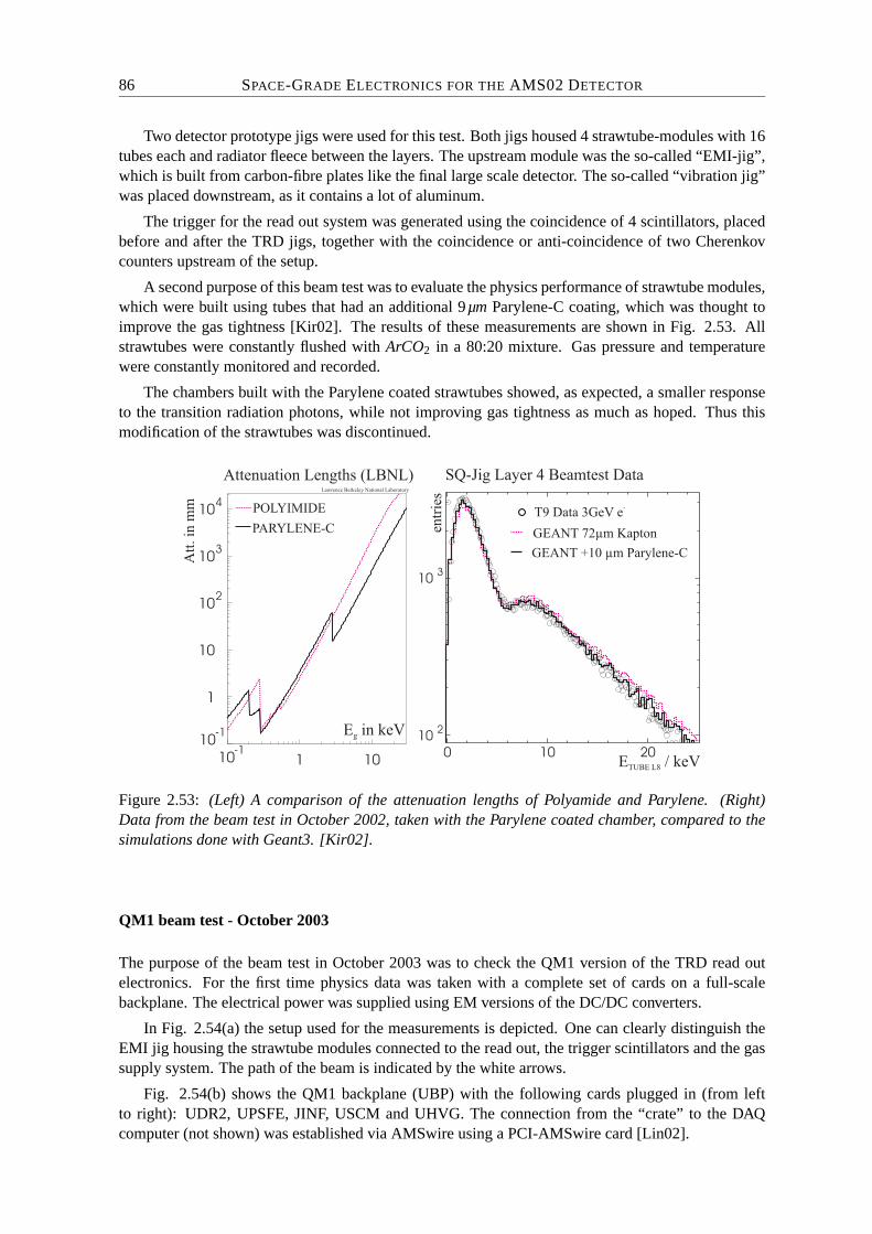
86 SPACE-GRADE ELECTRONICS FOR THE AMS02 DETECTOR
Two detector prototype jigs were used for this test. Both jigs housed 4 strawtube-modules with 16tubes each and radiator fleece between the layers. The upstream module was the so-called “EMI-jig”,which is built from carbon-fibre plates like the final large scale detector. The so-called “vibration jig”was placed downstream, as it contains a lot of aluminum.
The trigger for the read out system was generated using the coincidence of 4 scintillators, placedbefore and after the TRD jigs, together with the coincidence or anti-coincidence of two Cherenkovcounters upstream of the setup.
A second purpose of this beam test was to evaluate the physics performance of strawtube modules,which were built using tubes that had an additional 9µm Parylene-C coating, which was thought toimprove the gas tightness [Kir02]. The results of these measurements are shown in Fig. 2.53. Allstrawtubes were constantly flushed with ArCO2 in a 80:20 mixture. Gas pressure and temperaturewere constantly monitored and recorded.
The chambers built with the Parylene coated strawtubes showed, as expected, a smaller responseto the transition radiation photons, while not improving gas tightness as much as hoped. Thus thismodification of the strawtubes was discontinued.
10-1
1
10
102
103
104
10-1
1 100 10 20
Attenuation Lengths (LBNL)Lawrence Berkeley National Laboratory
Att
.in
mm POLYIMIDE
PARYLENE-C
E in keVg
entr
ies
SQ-Jig Layer 4 Beamtest Data
T9 Data 3GeV e-
GEANT 72µm Kapton
GEANT +10 µm Parylene-C
E / keVTUBE L8
Figure 2.53: (Left) A comparison of the attenuation lengths of Polyamide and Parylene. (Right)Data from the beam test in October 2002, taken with the Parylene coated chamber, compared to thesimulations done with Geant3. [Kir02].
QM1 beam test - October 2003
The purpose of the beam test in October 2003 was to check the QM1 version of the TRD read outelectronics. For the first time physics data was taken with a complete set of cards on a full-scalebackplane. The electrical power was supplied using EM versions of the DC/DC converters.
In Fig. 2.54(a) the setup used for the measurements is depicted. One can clearly distinguish theEMI jig housing the strawtube modules connected to the read out, the trigger scintillators and the gassupply system. The path of the beam is indicated by the white arrows.
Fig. 2.54(b) shows the QM1 backplane (UBP) with the following cards plugged in (from leftto right): UDR2, UPSFE, JINF, USCM and UHVG. The connection from the “crate” to the DAQcomputer (not shown) was established via AMSwire using a PCI-AMSwire card [Lin02].
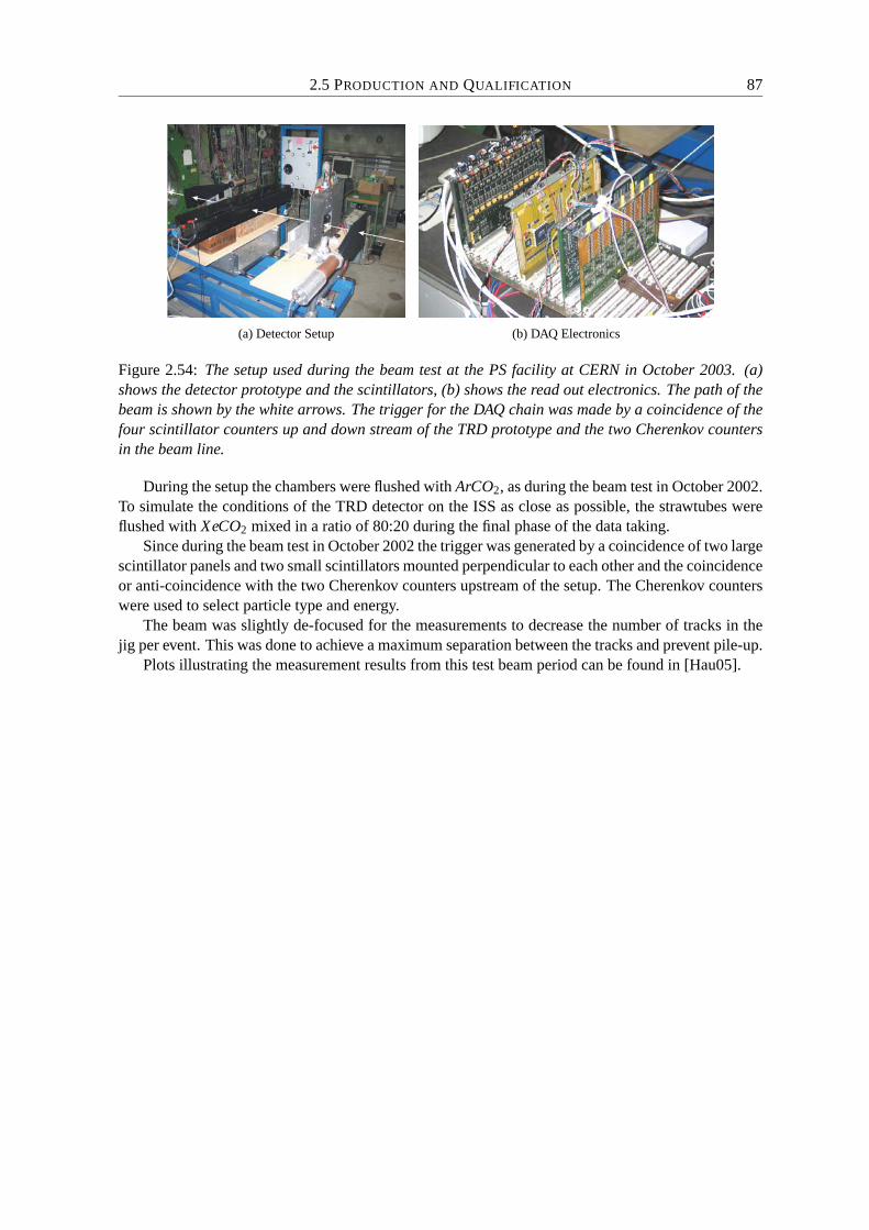
2.5 PRODUCTION AND QUALIFICATION 87
(a) Detector Setup (b) DAQ Electronics
Figure 2.54: The setup used during the beam test at the PS facility at CERN in October 2003. (a)shows the detector prototype and the scintillators, (b) shows the read out electronics. The path of thebeam is shown by the white arrows. The trigger for the DAQ chain was made by a coincidence of thefour scintillator counters up and down stream of the TRD prototype and the two Cherenkov countersin the beam line.
During the setup the chambers were flushed with ArCO2, as during the beam test in October 2002.To simulate the conditions of the TRD detector on the ISS as close as possible, the strawtubes wereflushed with XeCO2 mixed in a ratio of 80:20 during the final phase of the data taking.
Since during the beam test in October 2002 the trigger was generated by a coincidence of two largescintillator panels and two small scintillators mounted perpendicular to each other and the coincidenceor anti-coincidence with the two Cherenkov counters upstream of the setup. The Cherenkov counterswere used to select particle type and energy.
The beam was slightly de-focused for the measurements to decrease the number of tracks in thejig per event. This was done to achieve a maximum separation between the tracks and prevent pile-up.
Plots illustrating the measurement results from this test beam period can be found in [Hau05].


Chapter 3
Silicon Sensors
In this chapter, after an introduction into the interaction of radiation with matter, the most impor-tant features of position sensitive semiconductor radiation detectors will be presented, with a specialemphasis on CMOS Pixel Detectors, as these played a major role in the framework of this thesis.Following this is a section on the influence of radiation on the performance of the detection device.
An in-depth description of the properties of the semiconductor material silicon and detectors madefrom it can be found in [Lut99, Die03].
3.1 Interaction Of Radiation With Matter
A charged particle travelling at high speeds will lose energy, when it traverses matter. This happens inindependent stochastic processes, in which the incident particle interacts with either the electrons ofan atom of the target or its nucleus. In both types of interactions different processes contribute to thetotal loss of energy of the incident particle. In the following sections the mechanisms of energy losswill be described for charged particles and photons.
Unfortunately, the energy deposition of incident particles can also affect the detector itself. Theeffects of radiation on the detector and its performance will be introduced in section 3.4 at the end ofthis chapter.
3.1.1 Charged Particles
The principle mechanisms of energy loss are the same for light and heavy particles, even thoughsome processes (e.g. bremsstrahlung) only appear at relativistic velocities and thus mainly affect lightparticles, like electrons. The most important process for the energy loss of charged particles is aninelastic process in which the incident particle scatters at an orbital electron. In case the energytransfer to the target electron is large enough, it can be removed from the potential well of the atomand leave behind an ionised atom. If the energy transfer onto the target electron is above a few keV ,the knocked out electron is also called δ-electron(1). These δ-electrons cause themselves substantialsecondary ionisation. The second case, in which the energy transfer is not sufficient to ionise theatom, leads to excited states of the atom. In semiconductor materials these excited states can also bedescribed by a process in which an electron is lifted from the valence band to the conduction band,the creation of an electron-hole pair. In both cases the atom returns from its excited state to its defaultstate by the emission of photons or phonons.
The generation of free charge carriers via the above mentioned processes in the target material bythe incident particle is exploited in solid state and gaseous sensors for the detection of particles. Inmost solid state application this is done by depleting the sensitive volume from free charge carriers by
(1)In some books the δ-electrons are also called knock-on electrons.
89
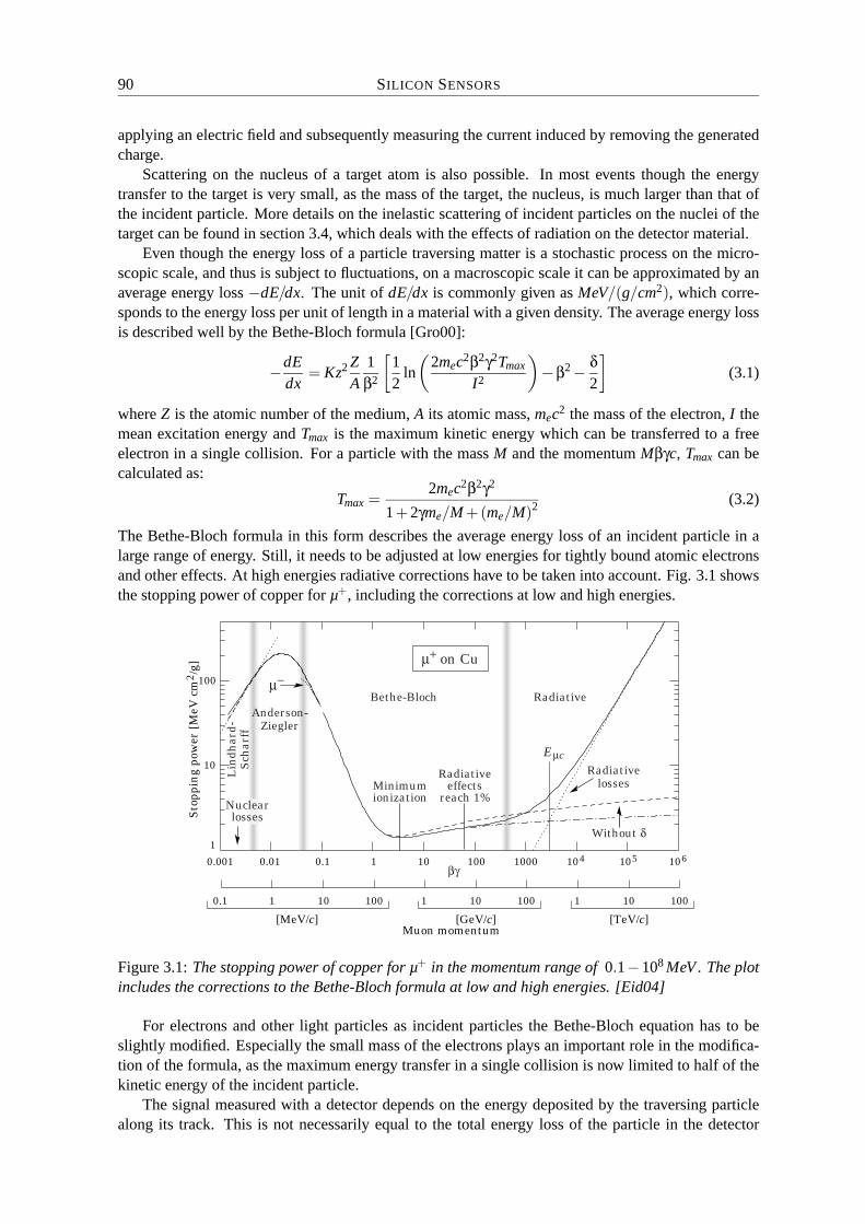
90 SILICON SENSORS
applying an electric field and subsequently measuring the current induced by removing the generatedcharge.
Scattering on the nucleus of a target atom is also possible. In most events though the energytransfer to the target is very small, as the mass of the target, the nucleus, is much larger than that ofthe incident particle. More details on the inelastic scattering of incident particles on the nuclei of thetarget can be found in section 3.4, which deals with the effects of radiation on the detector material.
Even though the energy loss of a particle traversing matter is a stochastic process on the micro-scopic scale, and thus is subject to fluctuations, on a macroscopic scale it can be approximated by anaverage energy loss −dE/dx. The unit of dE/dx is commonly given as MeV/(g/cm2), which corre-sponds to the energy loss per unit of length in a material with a given density. The average energy lossis described well by the Bethe-Bloch formula [Gro00]:
−dEdx
= Kz2 ZA
1β2
[12
ln
(2mec2β2γ2Tmax
I2
)−β2 − δ
2
](3.1)
where Z is the atomic number of the medium, A its atomic mass, mec2 the mass of the electron, I themean excitation energy and Tmax is the maximum kinetic energy which can be transferred to a freeelectron in a single collision. For a particle with the mass M and the momentum Mβγc, Tmax can becalculated as:
Tmax =2mec2β2γ2
1+2γme/M +(me/M)2 (3.2)
The Bethe-Bloch formula in this form describes the average energy loss of an incident particle in alarge range of energy. Still, it needs to be adjusted at low energies for tightly bound atomic electronsand other effects. At high energies radiative corrections have to be taken into account. Fig. 3.1 showsthe stopping power of copper for µ+, including the corrections at low and high energies.
Muon momentum
1
10
100
Sto
ppin
g po
wer
[M
eV c
m2 /
g]
Lin
dhar
d-S
char
ff
Bethe-Bloch Radiative
Radiativeeffects
reach 1%
µ+ on Cu
Without δ
Radiativelosses
βγ0.001 0.01 0.1 1 10 100 1000 104 105 106
[MeV/c] [GeV/c]
1001010.1 100101 100101
[TeV/c]
Anderson-Ziegler
Nuclearlosses
Minimumionization
Eµc
µ−
Figure 3.1: The stopping power of copper for µ+ in the momentum range of 0.1−108 MeV. The plotincludes the corrections to the Bethe-Bloch formula at low and high energies. [Eid04]
For electrons and other light particles as incident particles the Bethe-Bloch equation has to beslightly modified. Especially the small mass of the electrons plays an important role in the modifica-tion of the formula, as the maximum energy transfer in a single collision is now limited to half of thekinetic energy of the incident particle.
The signal measured with a detector depends on the energy deposited by the traversing particlealong its track. This is not necessarily equal to the total energy loss of the particle in the detector
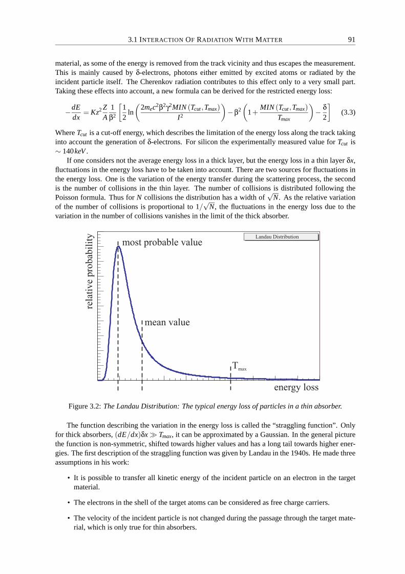
3.1 INTERACTION OF RADIATION WITH MATTER 91
material, as some of the energy is removed from the track vicinity and thus escapes the measurement.This is mainly caused by δ-electrons, photons either emitted by excited atoms or radiated by theincident particle itself. The Cherenkov radiation contributes to this effect only to a very small part.Taking these effects into account, a new formula can be derived for the restricted energy loss:
−dEdx
= Kz2 ZA
1β2
[12
ln
(2mec2β2γ2MIN (Tcut ,Tmax)
I2
)−β2
(1+
MIN (Tcut ,Tmax)Tmax
)− δ
2
](3.3)
Where Tcut is a cut-off energy, which describes the limitation of the energy loss along the track takinginto account the generation of δ-electrons. For silicon the experimentally measured value for Tcut is∼ 140keV .
If one considers not the average energy loss in a thick layer, but the energy loss in a thin layer δx,fluctuations in the energy loss have to be taken into account. There are two sources for fluctuations inthe energy loss. One is the variation of the energy transfer during the scattering process, the secondis the number of collisions in the thin layer. The number of collisions is distributed following thePoisson formula. Thus for N collisions the distribution has a width of
√N. As the relative variation
of the number of collisions is proportional to 1/√
N, the fluctuations in the energy loss due to thevariation in the number of collisions vanishes in the limit of the thick absorber.
0
Landau Distribution
energy loss
mean value
most probable value
rela
tiv
ep
rob
abil
ity
Tmax
Figure 3.2: The Landau Distribution: The typical energy loss of particles in a thin absorber.
The function describing the variation in the energy loss is called the “straggling function”. Onlyfor thick absorbers, (dE/dx)δx Tmax, it can be approximated by a Gaussian. In the general picturethe function is non-symmetric, shifted towards higher values and has a long tail towards higher ener-gies. The first description of the straggling function was given by Landau in the 1940s. He made threeassumptions in his work:
• It is possible to transfer all kinetic energy of the incident particle on an electron in the targetmaterial.
• The electrons in the shell of the target atoms can be considered as free charge carriers.
• The velocity of the incident particle is not changed during the passage through the target mate-rial, which is only true for thin absorbers.
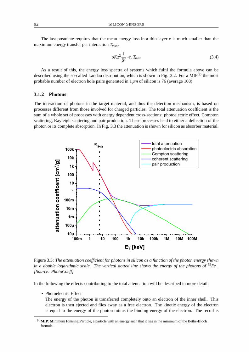
92 SILICON SENSORS
The last postulate requires that the mean energy loss in a thin layer x is much smaller than themaximum energy transfer per interaction Tmax.
ρKz2 1β2 Tmax (3.4)
As a result of this, the energy loss spectra of systems which fulfil the formula above can bedescribed using the so-called Landau distribution, which is shown in Fig. 3.2. For a MIP(2) the mostprobable number of electron hole pairs generated in 1µm of silicon is 76 (average 108).
3.1.2 Photons
The interaction of photons in the target material, and thus the detection mechanism, is based onprocesses different from those involved for charged particles. The total attenuation coefficient is thesum of a whole set of processes with energy dependent cross-sections: photoelectric effect, Comptonscattering, Rayleigh scattering and pair production. These processes lead to either a deflection of thephoton or its complete absorption. In Fig. 3.3 the attenuation is shown for silicon as absorber material.
Figure 3.3: The attenuation coefficient for photons in silicon as a function of the photon energy shownin a double logarithmic scale. The vertical dotted line shows the energy of the photons of 55Fe .[Source: PhotoCoeff]
In the following the effects contributing to the total attenuation will be described in more detail:
• Photoelectric EffectThe energy of the photon is transferred completely onto an electron of the inner shell. Thiselectron is then ejected and flies away as a free electron. The kinetic energy of the electronis equal to the energy of the photon minus the binding energy of the electron. The recoil is
(2)MIP: Minimum Ionising Particle, a particle with an energy such that it lies in the minimum of the Bethe-Blochformula.

3.1 INTERACTION OF RADIATION WITH MATTER 93
absorbed by the nucleus to which the electron was bound. If the resulting photoelectron hasenough kinetic energy, it will produce secondary ionisation along its track. As the completeenergy of the photon is absorbed in one step, this process can be used for the calibration ofthe detector. Nevertheless, the result may be smeared by escaping photons. These photons areproduced, when the hole in the electron shell of the nucleus is filled again by an electron froman outer shell “falling down”. The energy of the second generation photons is much smallerthan that of the incident one.
• Compton ScatteringIn the Compton effect, also called the incoherent scattering, the incident photon scatters on afree electron(3) in the absorber material. In this process the photon transfers some of its energyonto the electron, but it is not fully absorbed, it continues its path albeit under an angle to itsincident trajectory. The target atom is partially ionised after a Compton scattering, as the “free”electron flies away.
• Rayleigh ScatteringThe Rayleigh scattering (or coherent scattering) is also based on the interaction of an incidentphoton with an electron of the shell of the atom. Unlike in the Compton scattering, in thiseffect no energy is transferred onto the medium, neither is the atom excited nor ionised, onlythe photon is deflected from its original path.
• Pair ProductionDuring the process of pair production a photon is transformed into an electron and a positron.Since momentum has to be conserved in this process, it can only happen in the presence of athird body, to be more exact, in the Coulomb field of a nucleus or an electron. As two particlesare produced in this process, the energy of the incident photon has to be larger than the threshold,which is given by two times the rest mass of the electron (∼ 1.02MeV ).
The most commonly used soft X-ray photons for detector calibration are those from the two decaylines of 55Fe . With a characteristic energy of 5.9keV (branching ratio 24.4%) and 6.49keV (branchingratio 2.86%) they have an absorption length in silicon of 26.95µm and 35.35µm respectively. InCMOS detectors, this allows to probe the whole depth of the active volume which has a typicalthickness of < 15µm beneath a dead layer of < 10µm, which consists of the integrated electronics andpassivation layers. A typical 55Fe spectrum measured with a CMOS detector is shown in Fig. 3.9.
The size of the charge cloud generated by the absorption of a X-ray photon is given by the rangein the detector material of the secondary electrons produced in the absorption process. The range R ofa secondary electron with the energy Ee− is given by [Bro61]:
R = 40.8 ·10−3 µm ·Ee− [keV ] (3.5)
Thus for secondary electrons generated during the absorption of 55Fe gammas, the range is smallerthan 1µm, which leads to a charge cloud confined very closely around the absorption point of theX-ray photon.
3.1.3 Charge Carrier Generation in Semiconductor Materials
In semiconductor detectors the generation of electron-hole (e-h) pairs by the incident particle itself orsecondary effects, due to its passage through the material, is used for the detection of high energeticparticles. The energy W required to generate one e-h pair depends strongly on the material used, as
(3)Actually, it is an electron bound to a nucleus, but if the energy of the incident photon is large compared to thebinding energy, the electron can be considered approximately as free.
94 SILICON SENSORS
it is a function of the band gap and thus slightly depends on the temperature of the device. Eqn. 3.6gives a linear fit to the data measured for various materials [Ali80].
W = 1.76eV +1.84 ·Egap (3.6)
As one can see from the equation above, the energy needed to create an e-h pair in a semiconductoris always larger than the band gap. This is due to the fact, that there is a distinct possibility to invokeadditional processes involving the excitation of phonons(4) and plasmons(5). While the measurableeffect of phonons in the detector is an increase in the temperature of the device, plasmons end upproducing e-h pairs with relatively high energies. The electrons created in this process are called “hotelectrons” due to the higher energy.
The mean energy required to produce one e-h pair in silicon was measured to be W = 3.658eVat 170K with a temperature dependence of dW/dT = −0.1%/K [Fra94]. This corresponds to W =3.645eV at room temperature.
The intrinsic energy resolution ∆E is given by the following expression:
∆E = 2.36√
N with N =EW
(3.7)
Where N is the number of primary e-h pairs produced in the absorption, E the total energy absorbedand W the energy required to produce an e-h pair. This equation assumes a Poisson distribution of thenumber of interactions where σn =
√n is the variation of a given number n. The statistical accuracy
is improved by the introduction of the Fano factor f , which was experimentally determined to bef = 0.155.
∆E = 2.36√
N · f (3.8)
For the total energy resolution of the detector, one of course has to take into account further effects,e.g. variations in the detector material, in the gain of the read out channels and the noise of the deviceitself and its read out system.
3.2 Position Sensitive Detectors
Charged particles travelling at relativistic velocities generate charge carrier pairs when traversing con-densed matter along their track and small clouds of charge carriers at the position where they arestopped, see section 3.1 for more details. Thus a segmented detection device allows to determine theposition where the particle interacted in the sensitive volume. In the following sections various typesof position sensitive devices will be introduced.
3.2.1 Microstrip Detectors
Silicon microstrip detectors, see Fig. 3.4, are the most commonly used position sensitive radiationdetectors in High Energy Physics. In experiments like DELPHI and CDF they have proven their reli-ability. As a consequence, they are also used in the next generation of experiments (CMS, ATLAS,...)at CERN.
Microstrip detectors are large area diodes, with a sensitive area of up to 100cm2, operated inreverse bias mode with a typical thickness of 300µm. The implants and contacts of the diode aresegmented into multiple thin strips to obtain a high spatial resolution. The pitch, the distance from one
(4)Phonons are the quanta of the lattice oscillations. They are classified in two groups: the acoustic and the opticalphonos. The acoustic phonos are related to the propagation of sound waves in the lattice, the second class ofphonons can interact directly or indirectly with photons and thus are named optical phonons. They occur incrystals with more than one atom per unit cell.
(5)The quanta of the longitudinal oscillations of the free electron gas in the semiconductor crystal are calledplasmons. The typical energy range for plasmons is 3−20eV . In silicon they have an energy of 16.8eV .
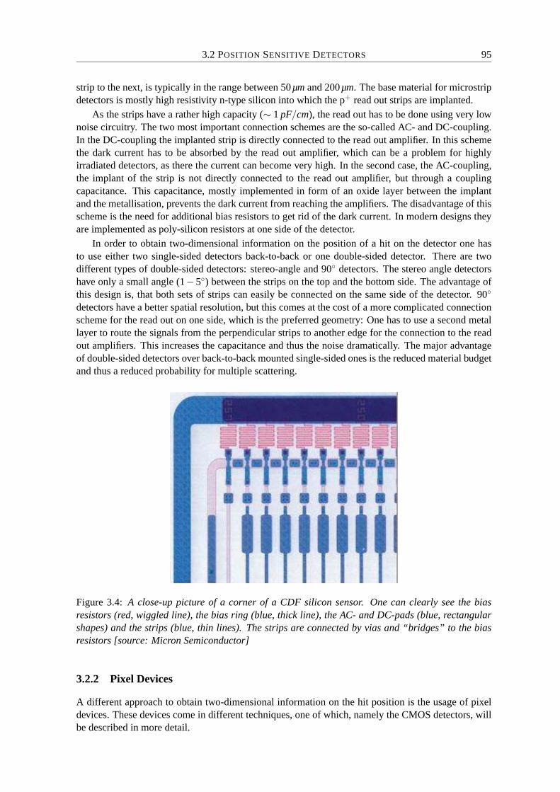
3.2 POSITION SENSITIVE DETECTORS 95
strip to the next, is typically in the range between 50µm and 200µm. The base material for microstripdetectors is mostly high resistivity n-type silicon into which the p+ read out strips are implanted.
As the strips have a rather high capacity (∼ 1 pF/cm), the read out has to be done using very lownoise circuitry. The two most important connection schemes are the so-called AC- and DC-coupling.In the DC-coupling the implanted strip is directly connected to the read out amplifier. In this schemethe dark current has to be absorbed by the read out amplifier, which can be a problem for highlyirradiated detectors, as there the current can become very high. In the second case, the AC-coupling,the implant of the strip is not directly connected to the read out amplifier, but through a couplingcapacitance. This capacitance, mostly implemented in form of an oxide layer between the implantand the metallisation, prevents the dark current from reaching the amplifiers. The disadvantage of thisscheme is the need for additional bias resistors to get rid of the dark current. In modern designs theyare implemented as poly-silicon resistors at one side of the detector.
In order to obtain two-dimensional information on the position of a hit on the detector one hasto use either two single-sided detectors back-to-back or one double-sided detector. There are twodifferent types of double-sided detectors: stereo-angle and 90 detectors. The stereo angle detectorshave only a small angle (1−5) between the strips on the top and the bottom side. The advantage ofthis design is, that both sets of strips can easily be connected on the same side of the detector. 90
detectors have a better spatial resolution, but this comes at the cost of a more complicated connectionscheme for the read out on one side, which is the preferred geometry: One has to use a second metallayer to route the signals from the perpendicular strips to another edge for the connection to the readout amplifiers. This increases the capacitance and thus the noise dramatically. The major advantageof double-sided detectors over back-to-back mounted single-sided ones is the reduced material budgetand thus a reduced probability for multiple scattering.
Figure 3.4: A close-up picture of a corner of a CDF silicon sensor. One can clearly see the biasresistors (red, wiggled line), the bias ring (blue, thick line), the AC- and DC-pads (blue, rectangularshapes) and the strips (blue, thin lines). The strips are connected by vias and “bridges” to the biasresistors [source: Micron Semiconductor]
3.2.2 Pixel Devices
A different approach to obtain two-dimensional information on the hit position is the usage of pixeldevices. These devices come in different techniques, one of which, namely the CMOS detectors, willbe described in more detail.
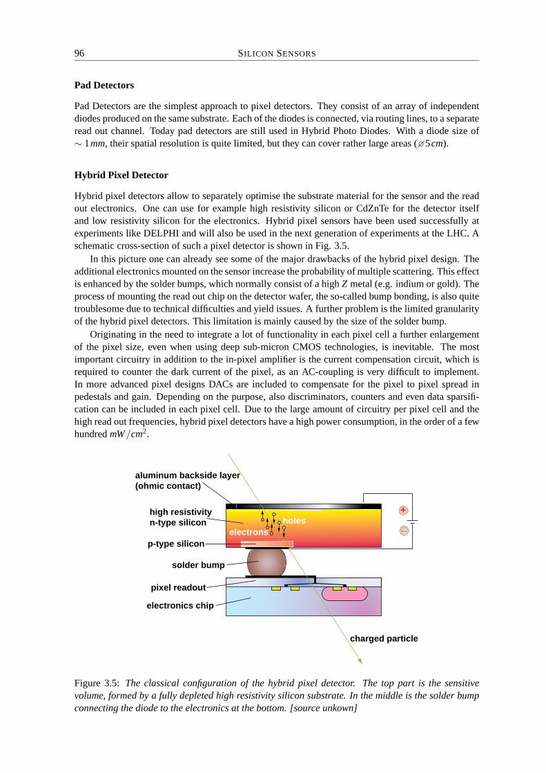
96 SILICON SENSORS
Pad Detectors
Pad Detectors are the simplest approach to pixel detectors. They consist of an array of independentdiodes produced on the same substrate. Each of the diodes is connected, via routing lines, to a separateread out channel. Today pad detectors are still used in Hybrid Photo Diodes. With a diode size of∼ 1mm, their spatial resolution is quite limited, but they can cover rather large areas (5cm).
Hybrid Pixel Detector
Hybrid pixel detectors allow to separately optimise the substrate material for the sensor and the readout electronics. One can use for example high resistivity silicon or CdZnTe for the detector itselfand low resistivity silicon for the electronics. Hybrid pixel sensors have been used successfully atexperiments like DELPHI and will also be used in the next generation of experiments at the LHC. Aschematic cross-section of such a pixel detector is shown in Fig. 3.5.
In this picture one can already see some of the major drawbacks of the hybrid pixel design. Theadditional electronics mounted on the sensor increase the probability of multiple scattering. This effectis enhanced by the solder bumps, which normally consist of a high Z metal (e.g. indium or gold). Theprocess of mounting the read out chip on the detector wafer, the so-called bump bonding, is also quitetroublesome due to technical difficulties and yield issues. A further problem is the limited granularityof the hybrid pixel detectors. This limitation is mainly caused by the size of the solder bump.
Originating in the need to integrate a lot of functionality in each pixel cell a further enlargementof the pixel size, even when using deep sub-micron CMOS technologies, is inevitable. The mostimportant circuitry in addition to the in-pixel amplifier is the current compensation circuit, which isrequired to counter the dark current of the pixel, as an AC-coupling is very difficult to implement.In more advanced pixel designs DACs are included to compensate for the pixel to pixel spread inpedestals and gain. Depending on the purpose, also discriminators, counters and even data sparsifi-cation can be included in each pixel cell. Due to the large amount of circuitry per pixel cell and thehigh read out frequencies, hybrid pixel detectors have a high power consumption, in the order of a fewhundred mW/cm2.
pixel readout
holeselectrons
aluminum backside layer(ohmic contact)
high resistivityn-type silicon
pixel readout
electronics chip
+
_p-type silicon
charged particle
solder bump
Figure 3.5: The classical configuration of the hybrid pixel detector. The top part is the sensitivevolume, formed by a fully depleted high resistivity silicon substrate. In the middle is the solder bumpconnecting the diode to the electronics at the bottom. [source unkown]
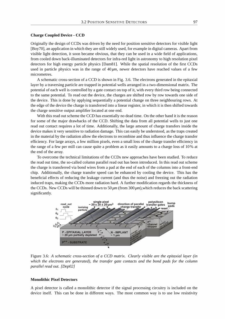
3.2 POSITION SENSITIVE DETECTORS 97
Charge Coupled Device - CCD
Originally the design of CCDs was driven by the need for position sensitive detectors for visible light[Boy70], an application in which they are still widely used, for example in digital cameras. Apart fromvisible light detection, it soon became obvious, that they can be used in a wide field of applications,from cooled down back-illuminated detectors for infra-red light in astronomy to high resolution pixeldetectors for high energy particle physics [Dam81]. While the spatial resolution of the first CCDsused in particle physics was in the range of 40µm, newer detectors have reached values of a fewmicrometres.
A schematic cross-section of a CCD is shown in Fig. 3.6. The electrons generated in the epitaxiallayer by a traversing particle are trapped in potential wells arranged in a two-dimensional matrix. Thepotential of each well is controlled by a gate contact on top of it, with every third row being connectedto the same potential. To read out the device, the charges are shifted row by row towards one side ofthe device. This is done by applying sequentially a potential change on three neighbouring rows. Atthe edge of the device the charge is transferred into a linear register, in which it is then shifted towardsthe charge sensitive output amplifier located at one end.
With this read out scheme the CCD has essentially no dead time. On the other hand it is the reasonfor some of the major drawbacks of the CCD. Shifting the data from all potential wells to just oneread out contact requires a lot of time. Additionally, the large amount of charge transfers inside thedevice makes it very sensitive to radiation damage. This can easily be understood, as the traps createdin the material by the radiation allow the electrons to recombine and thus influence the charge transferefficiency. For large arrays, a few million pixels, even a small loss of the charge transfer efficiency inthe range of a few per mill can cause quite a problem as it easily amounts to a charge loss of 10% atthe end of the array.
To overcome the technical limitations of the CCDs new approaches have been studied. To reducethe read out time, the so-called column parallel read out has been introduced. In this read out schemethe charge is transferred via bond wires from a pad at the end of each of the columns into a front-endchip. Additionally, the charge transfer speed can be enhanced by cooling the device. This has thebeneficial effects of reducing the leakage current (and thus the noise) and freezing out the radiationinduced traps, making the CCDs more radiation hard. A further modification regards the thickness ofthe CCDs. New CCDs will be thinned down to 50µm (from 300µm),which reduces the back scatteringsignificantly.
Figure 3.6: A schematic cross-section of a CCD matrix. Clearly visible are the epitaxial layer (inwhich the electrons are generated), the transfer gate contacts and the bond pads for the columnparallel read out. [Dep02]
Monolithic Pixel Detectors
A pixel detector is called a monolithic detector if the signal processing circuitry is included on thedevice itself. This can be done in different ways. The most common way is to use low resistivity
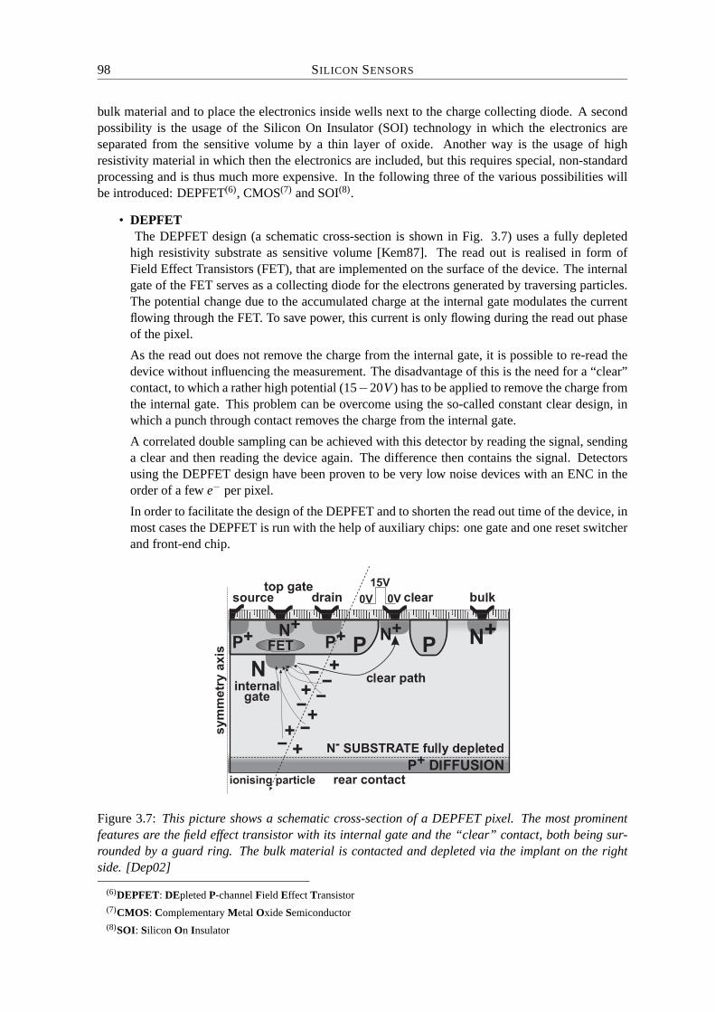
98 SILICON SENSORS
bulk material and to place the electronics inside wells next to the charge collecting diode. A secondpossibility is the usage of the Silicon On Insulator (SOI) technology in which the electronics areseparated from the sensitive volume by a thin layer of oxide. Another way is the usage of highresistivity material in which then the electronics are included, but this requires special, non-standardprocessing and is thus much more expensive. In the following three of the various possibilities willbe introduced: DEPFET(6), CMOS(7) and SOI(8).
• DEPFETThe DEPFET design (a schematic cross-section is shown in Fig. 3.7) uses a fully depleted
high resistivity substrate as sensitive volume [Kem87]. The read out is realised in form ofField Effect Transistors (FET), that are implemented on the surface of the device. The internalgate of the FET serves as a collecting diode for the electrons generated by traversing particles.The potential change due to the accumulated charge at the internal gate modulates the currentflowing through the FET. To save power, this current is only flowing during the read out phaseof the pixel.
As the read out does not remove the charge from the internal gate, it is possible to re-read thedevice without influencing the measurement. The disadvantage of this is the need for a “clear”contact, to which a rather high potential (15−20V ) has to be applied to remove the charge fromthe internal gate. This problem can be overcome using the so-called constant clear design, inwhich a punch through contact removes the charge from the internal gate.
A correlated double sampling can be achieved with this detector by reading the signal, sendinga clear and then reading the device again. The difference then contains the signal. Detectorsusing the DEPFET design have been proven to be very low noise devices with an ENC in theorder of a few e− per pixel.
In order to facilitate the design of the DEPFET and to shorten the read out time of the device, inmost cases the DEPFET is run with the help of auxiliary chips: one gate and one reset switcherand front-end chip.
Figure 3.7: This picture shows a schematic cross-section of a DEPFET pixel. The most prominentfeatures are the field effect transistor with its internal gate and the “clear” contact, both being sur-rounded by a guard ring. The bulk material is contacted and depleted via the implant on the rightside. [Dep02]
(6)DEPFET: DEpleted P-channel Field Effect Transistor(7)CMOS: Complementary Metal Oxide Semiconductor(8)SOI: Silicon On Insulator
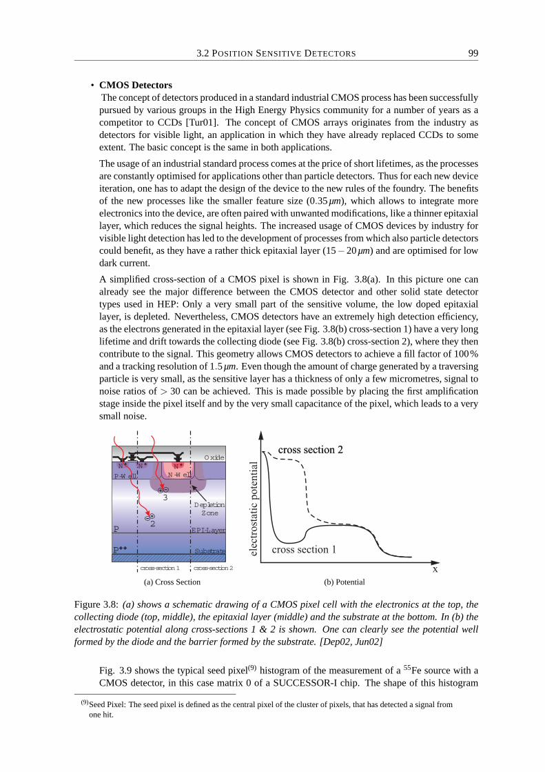
3.2 POSITION SENSITIVE DETECTORS 99
• CMOS DetectorsThe concept of detectors produced in a standard industrial CMOS process has been successfullypursued by various groups in the High Energy Physics community for a number of years as acompetitor to CCDs [Tur01]. The concept of CMOS arrays originates from the industry asdetectors for visible light, an application in which they have already replaced CCDs to someextent. The basic concept is the same in both applications.
The usage of an industrial standard process comes at the price of short lifetimes, as the processesare constantly optimised for applications other than particle detectors. Thus for each new deviceiteration, one has to adapt the design of the device to the new rules of the foundry. The benefitsof the new processes like the smaller feature size (0.35µm), which allows to integrate moreelectronics into the device, are often paired with unwanted modifications, like a thinner epitaxiallayer, which reduces the signal heights. The increased usage of CMOS devices by industry forvisible light detection has led to the development of processes from which also particle detectorscould benefit, as they have a rather thick epitaxial layer (15−20µm) and are optimised for lowdark current.
A simplified cross-section of a CMOS pixel is shown in Fig. 3.8(a). In this picture one canalready see the major difference between the CMOS detector and other solid state detectortypes used in HEP: Only a very small part of the sensitive volume, the low doped epitaxiallayer, is depleted. Nevertheless, CMOS detectors have an extremely high detection efficiency,as the electrons generated in the epitaxial layer (see Fig. 3.8(b) cross-section 1) have a very longlifetime and drift towards the collecting diode (see Fig. 3.8(b) cross-section 2), where they thencontribute to the signal. This geometry allows CMOS detectors to achieve a fill factor of 100%and a tracking resolution of 1.5µm. Even though the amount of charge generated by a traversingparticle is very small, as the sensitive layer has a thickness of only a few micrometres, signal tonoise ratios of > 30 can be achieved. This is made possible by placing the first amplificationstage inside the pixel itself and by the very small capacitance of the pixel, which leads to a verysmall noise.
Oxide
N-W ellNNN
P-W ell
EPI-Layer
Substrate
DepletionZone
P
P
cross-section 2cross-section 1
3
2
(a) Cross Section
cross section 2cross section 2
cross section 1elec
tro
stat
icp
ote
nti
al
(b) Potential
Figure 3.8: (a) shows a schematic drawing of a CMOS pixel cell with the electronics at the top, thecollecting diode (top, middle), the epitaxial layer (middle) and the substrate at the bottom. In (b) theelectrostatic potential along cross-sections 1 & 2 is shown. One can clearly see the potential wellformed by the diode and the barrier formed by the substrate. [Dep02, Jun02]
Fig. 3.9 shows the typical seed pixel(9) histogram of the measurement of a 55Fe source with aCMOS detector, in this case matrix 0 of a SUCCESSOR-I chip. The shape of this histogram
(9)Seed Pixel: The seed pixel is defined as the central pixel of the cluster of pixels, that has detected a signal fromone hit.
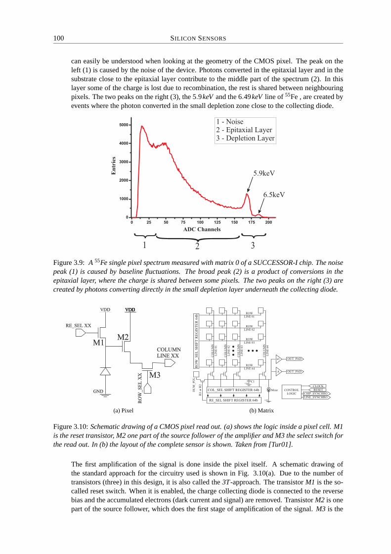
100 SILICON SENSORS
can easily be understood when looking at the geometry of the CMOS pixel. The peak on theleft (1) is caused by the noise of the device. Photons converted in the epitaxial layer and in thesubstrate close to the epitaxial layer contribute to the middle part of the spectrum (2). In thislayer some of the charge is lost due to recombination, the rest is shared between neighbouringpixels. The two peaks on the right (3), the 5.9keV and the 6.49keV line of 55Fe , are created byevents where the photon converted in the small depletion zone close to the collecting diode.
1 2 3
5.9keV
6.5keV
1 - Noise2 - Epitaxial Layer3 - Depletion Layer
En
trie
s
ADC Channels
Figure 3.9: A 55Fe single pixel spectrum measured with matrix 0 of a SUCCESSOR-I chip. The noisepeak (1) is caused by baseline fluctuations. The broad peak (2) is a product of conversions in theepitaxial layer, where the charge is shared between some pixels. The two peaks on the right (3) arecreated by photons converting directly in the small depletion layer underneath the collecting diode.
(a) Pixel (b) Matrix
Figure 3.10: Schematic drawing of a CMOS pixel read out. (a) shows the logic inside a pixel cell. M1is the reset transistor, M2 one part of the source follower of the amplifier and M3 the select switch forthe read out. In (b) the layout of the complete sensor is shown. Taken from [Tur01].
The first amplification of the signal is done inside the pixel itself. A schematic drawing ofthe standard approach for the circuitry used is shown in Fig. 3.10(a). Due to the number oftransistors (three) in this design, it is also called the 3T-approach. The transistor M1 is the so-called reset switch. When it is enabled, the charge collecting diode is connected to the reversebias and the accumulated electrons (dark current and signal) are removed. Transistor M2 is onepart of the source follower, which does the first stage of amplification of the signal. M3 is the
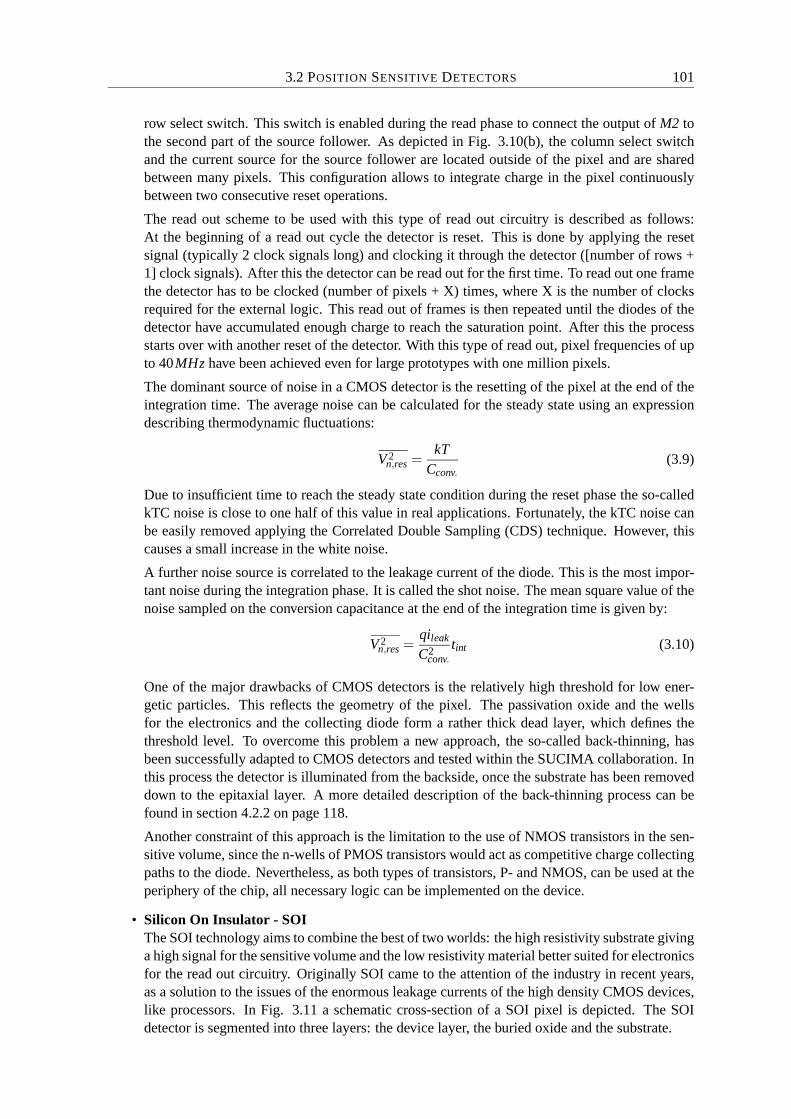
3.2 POSITION SENSITIVE DETECTORS 101
row select switch. This switch is enabled during the read phase to connect the output of M2 tothe second part of the source follower. As depicted in Fig. 3.10(b), the column select switchand the current source for the source follower are located outside of the pixel and are sharedbetween many pixels. This configuration allows to integrate charge in the pixel continuouslybetween two consecutive reset operations.
The read out scheme to be used with this type of read out circuitry is described as follows:At the beginning of a read out cycle the detector is reset. This is done by applying the resetsignal (typically 2 clock signals long) and clocking it through the detector ([number of rows +1] clock signals). After this the detector can be read out for the first time. To read out one framethe detector has to be clocked (number of pixels + X) times, where X is the number of clocksrequired for the external logic. This read out of frames is then repeated until the diodes of thedetector have accumulated enough charge to reach the saturation point. After this the processstarts over with another reset of the detector. With this type of read out, pixel frequencies of upto 40MHz have been achieved even for large prototypes with one million pixels.
The dominant source of noise in a CMOS detector is the resetting of the pixel at the end of theintegration time. The average noise can be calculated for the steady state using an expressiondescribing thermodynamic fluctuations:
V 2n,res =
kTCconv.
(3.9)
Due to insufficient time to reach the steady state condition during the reset phase the so-calledkTC noise is close to one half of this value in real applications. Fortunately, the kTC noise canbe easily removed applying the Correlated Double Sampling (CDS) technique. However, thiscauses a small increase in the white noise.
A further noise source is correlated to the leakage current of the diode. This is the most impor-tant noise during the integration phase. It is called the shot noise. The mean square value of thenoise sampled on the conversion capacitance at the end of the integration time is given by:
V 2n,res =
qileak
C2conv.
tint (3.10)
One of the major drawbacks of CMOS detectors is the relatively high threshold for low ener-getic particles. This reflects the geometry of the pixel. The passivation oxide and the wellsfor the electronics and the collecting diode form a rather thick dead layer, which defines thethreshold level. To overcome this problem a new approach, the so-called back-thinning, hasbeen successfully adapted to CMOS detectors and tested within the SUCIMA collaboration. Inthis process the detector is illuminated from the backside, once the substrate has been removeddown to the epitaxial layer. A more detailed description of the back-thinning process can befound in section 4.2.2 on page 118.
Another constraint of this approach is the limitation to the use of NMOS transistors in the sen-sitive volume, since the n-wells of PMOS transistors would act as competitive charge collectingpaths to the diode. Nevertheless, as both types of transistors, P- and NMOS, can be used at theperiphery of the chip, all necessary logic can be implemented on the device.
• Silicon On Insulator - SOIThe SOI technology aims to combine the best of two worlds: the high resistivity substrate givinga high signal for the sensitive volume and the low resistivity material better suited for electronicsfor the read out circuitry. Originally SOI came to the attention of the industry in recent years,as a solution to the issues of the enormous leakage currents of the high density CMOS devices,like processors. In Fig. 3.11 a schematic cross-section of a SOI pixel is depicted. The SOIdetector is segmented into three layers: the device layer, the buried oxide and the substrate.
102 SILICON SENSORS
In the first step of the production the SOI wafer is prepared. At the moment there are threecompeting techniques for this step. In the so-called SIMOX(10) process a layer with a highdose of oxygen is created by ion implantation. From this layer the BOX(11) is then formed byannealing of the wafer at high temperatures.
Alternatively, a SOI wafer can be fabricated by the so-called wafer bonding. In this process twowafers are “glued” together by oxidising them and bringing them into close contact, so that vander Waals forces keep them together. An annealing at this stage can improve the mechanicalstability. Afterwards the low resistivity device wafer is thinned down to the necessary level.This is done either by wet etching or by splitting. The second method, the splitting of the wafer,requires the introduction of a weak layer in the device wafer. This can be achieved by theimplantation of light ions or by anodic etching and annealing.
A further, but somewhat disfavoured, approach is ZMR(12), a process in which first an oxide isgrown on top of the wafer and then an amorphous layer of silicon on top of the oxide. Thisamorphous layer is then crystallised by heating the wafer locally above the melting point.
From the SOI wafer the pixel detector is then produced by etching the vias through the devicelayer and the BOX to the substrate for the pixel contact, the implantation of the pixel diodes andfinally the production of the electronics in the device layer. During all these steps the parametersof the process, especially the temperature, must be monitored closely.
While the production of SOI detectors is not a standard process, and not all parameters are fullyunderstood up to now, the SOI technique allows to employ both P- and NMOS transistors in thedevice layer, which makes it feasible to use much more complex electronics inside the pixel,than with only one type of transistors as in the CMOS pixel detector design.
Figure 3.11: A schematic cross-section of a SOI pixel. From top to bottom the following parts arevisible: the electronics layer, the buried oxide (BOX) and the high resistivity substrate with the diodesand the backside metallisation. [Mar04]
3.3 A Comparison of Detector Technologies
In order to select the best detector for a given purpose it is very important to carefully weigh the ad-vantages and disadvantages of each technology available against each other. Tab. 3.1 tries to give acomprehensive overview of the most popular technologies for particle detection. Based on conside-rations like these, SUCIMA decided to go for the CMOS technology for its main device and SOI ascandidate for the next generation of devices.
(10)SIMOX: Separation by IMplanted OXygen(11)BOX: Buried OXide(12)ZMR: Zone Melt Re-crystallisation
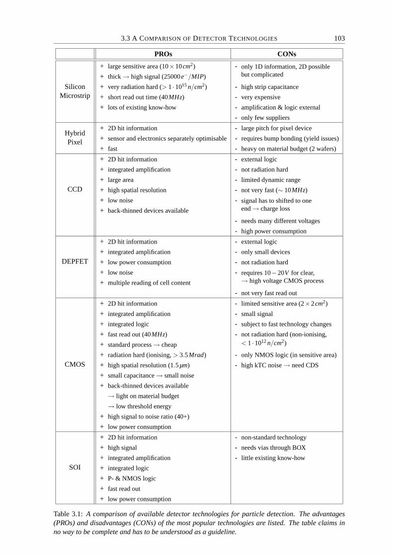
3.3 A COMPARISON OF DETECTOR TECHNOLOGIES 103
PROs CONs
SiliconMicrostrip
+ large sensitive area (10×10cm2) - only 1D information, 2D possiblebut complicated+ thick → high signal (25000e−/MIP)
+ very radiation hard (> 1 ·1015 n/cm2) - high strip capacitance
+ short read out time (40MHz) - very expensive
+ lots of existing know-how - amplification & logic external
- only few suppliers
HybridPixel
+ 2D hit information - large pitch for pixel device
+ sensor and electronics separately optimisable - requires bump bonding (yield issues)
+ fast - heavy on material budget (2 wafers)
CCD
+ 2D hit information - external logic
+ integrated amplification - not radiation hard
+ large area - limited dynamic range
+ high spatial resolution - not very fast (∼ 10MHz)
+ low noise - signal has to shifted to oneend → charge loss+ back-thinned devices available
- needs many different voltages
- high power consumption
DEPFET
+ 2D hit information - external logic
+ integrated amplification - only small devices
+ low power consumption - not radiation hard
+ low noise - requires 10−20V for clear,→ high voltage CMOS process+ multiple reading of cell content
- not very fast read out
CMOS
+ 2D hit information - limited sensitive area (2×2cm2)
+ integrated amplification - small signal
+ integrated logic - subject to fast technology changes
+ fast read out (40MHz) - not radiation hard (non-ionising,< 1 ·1012 n/cm2)+ standard process → cheap
+ radiation hard (ionising, > 3.5Mrad) - only NMOS logic (in sensitive area)
+ high spatial resolution (1.5µm) - high kTC noise → need CDS
+ small capacitance → small noise
+ back-thinned devices available
→ light on material budget
→ low threshold energy
+ high signal to noise ratio (40+)
+ low power consumption
SOI
+ 2D hit information - non-standard technology
+ high signal - needs vias through BOX
+ integrated amplification - little existing know-how
+ integrated logic
+ P- & NMOS logic
+ fast read out
+ low power consumption
Table 3.1: A comparison of available detector technologies for particle detection. The advantages(PROs) and disadvantages (CONs) of the most popular technologies are listed. The table claims inno way to be complete and has to be understood as a guideline.

104 SILICON SENSORS
3.4 Radiation Damage
In HEP experiments, as well as in other applications, the ability to withstand increasing radiationdoses has become a very important criterium for the design of solid state detectors, especially forthose made from silicon. The most severe requirements up to now on the radiation hardness areimposed on the detectors by the new generation of experiments at the LHC at CERN. There, a fluxof 1 · 1015 hadrons(13) and a total absorbed dose of 35Mrad is expected for the innermost layer ofthe vertex detector. But also in medical applications, like those envisaged by SUCIMA, the detectorperformance under the influence of radiation plays an important role.
Semiconductor devices are affected by three main effects under the influence of radiation: dis-placement of atoms from their positions in the lattice, transient and long term ionisation in insulatorlayers and formation of interface defects. The displacement of atoms is an issue, especially for lowerdoses, primarily in the bulk material of the detector and not in the read out electronics and thus it isalso called “bulk damage”. The inducing of locally fixed charge carriers by ionisation and the creationof interface defects is summarised under the term “surface damage”. Especially the trapped chargecarriers, but also the interface defects, are responsible for the deterioration of electronic devices. Both,bulk and surface damage, can affect the performance of the device, decreasing the signal height andincreasing the leakage current and the noise in the device, thus leading to a smaller signal to noiseratio.
In the following two sections both types of radiation induced damage in the device will be intro-duced. Also their influence on the performance of a device will be described, with an emphasis onCMOS detectors. For a more detailed reading please refer to [Lut99, Die03, Dep02].
The surface damage is by far the dominant effect of radiation damage in the applications ofSUCIMA. The radioactive sources used in clinical treatment emit only electrons and gammas of lowto medium energy. Thus the probability of bulk damage is extremely small. Nevertheless, the effectof neutron irradiation has been studied by Lepsi for doses up to 1012 n/cm2.
3.4.1 Bulk Damage
To displace a silicon atom from its position in the lattice, a minimum recoil energy of 15eV is needed.Elastic scattering of incident high energetic charged or neutral particles at the lattice atom is the sourceof the required energy. As the recoil energy needed to dislocate an atom is different in the directionof a neighbouring atom than in a direction between two atoms, the threshold is not sharp and thedisplacement energy Ed is introduced. For a value of Ed = 25eV the probability to displace an atom is0.5. For values below, lattice vibrations will dominate, while for values above, additionally interstitial-vacancy pairs will be formed. For recoil energies far above Ed , the displaced atom can cause furtherformation of interstitial-vacancy pairs.
If the recoil energy is below 1− 2keV , only isolated point defects will be created. For recoilenergies between 2 and 12keV , a defect cluster will be formed. These clusters consist of a denseagglomeration of point defects. Simulations give a diameter of 5nm of the cluster with roughly 100interstitial-vacancy pairs in it. They are formed at the end of the track of the recoil silicon atom, whereit loses its last 5−10keV and the cross-section increases by several orders of magnitude.
In Fig. 3.12 an example is shown for a recoil energy much larger than 12keV . In this case theknock-on atom has an energy of 50keV . As one can see, the simulation predicts the formation ofmany clusters and additional point defects along the track of the knock-on atoms.
Depending on the type of the impinging particle and its energy, different mechanisms are involvedin the generation of the primary knock-on silicon atom, resulting in different probabilities for theinteraction. In the inset of Fig. 3.12 the two possible interactions are shown. Charged particles scatterat the (partially screened) electric potential of the nucleus, while neutral particles scatter elastically at
(13)The flux of hadrons (any kind, any energy) is normalised to neutrons with an energy of 1MeV using the NIELhypothesis, where NIEL stands for Non-Ionising Energy Loss, and is given in units of 1MeV neutrons/cm2.
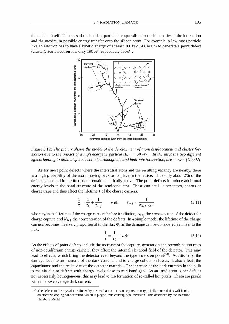
3.4 RADIATION DAMAGE 105
the nucleus itself. The mass of the incident particle is responsible for the kinematics of the interactionand the maximum possible energy transfer onto the silicon atom. For example, a low mass particlelike an electron has to have a kinetic energy of at least 260keV (4.6MeV ) to generate a point defect(cluster). For a neutron it is only 190eV respectively 15keV .
Figure 3.12: The picture shows the model of the development of atom displacement and cluster for-mation due to the impact of a high energetic particle (Ekin = 50keV). In the inset the two differenteffects leading to atom displacement, electromagnetic and hadronic interaction, are shown. [Dep02]
As for most point defects where the interstitial atom and the resulting vacancy are nearby, thereis a high probability of the atom moving back to its place in the lattice. Thus only about 2% of thedefects generated in the first place remain electrically active. The point defects introduce additionalenergy levels in the band structure of the semiconductor. These can act like acceptors, donors orcharge traps and thus affect the lifetime τ of the charge carriers.
1τ
=1τ0
+1
τde fwith τde f ∝
1σde f Nde f
(3.11)
where τ0 is the lifetime of the charge carriers before irradiation, σde f the cross-section of the defect forcharge capture and Nde f the concentration of the defects. In a simple model the lifetime of the chargecarriers becomes inversely proportional to the flux Φ, as the damage can be considered as linear to theflux.
1τ
=1τ0
+κτΦ (3.12)
As the effects of point defects include the increase of the capture, generation and recombination ratesof non-equilibrium charge carriers, they affect the internal electrical field of the detector. This maylead to effects, which bring the detector even beyond the type inversion point(14). Additionally, thedamage leads to an increase of the dark currents and to charge collection losses. It also affects thecapacitance and the resistivity of the detector material. The increase of the dark currents in the bulkis mainly due to defects with energy levels close to mid band gap. As an irradiation is per defaultnot necessarily homogeneous, this may lead to the formation of so-called hot pixels. These are pixelswith an above average dark current.
(14)The defects in the crystal introduced by the irradiation act as acceptors. In n-type bulk material this will lead toan effective doping concentration which is p-type, thus causing type inversion. This described by the so-calledHamburg Model
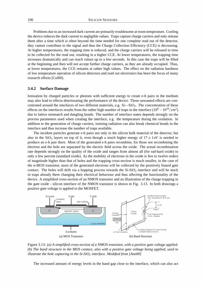
106 SILICON SENSORS
Problems due to an increased dark current are primarily troublesome at room temperature. Coolingthe device reduces the dark current to negligible values. Traps capture charge carriers and only releasethem after a time which is often beyond the time needed for one complete read out of the detector,they cannot contribute to the signal and thus the Charge Collection Efficiency (CCE) is decreasing.At higher temperatures, the trapping time is reduced, and the charge carriers will be released in timeto be collected for the read out, resulting in a higher CCE. At lower temperatures, the trapping timeincreases dramatically and can reach values up to a few seconds. In this case the traps will be filledat the beginning and then will not accept further charge carriers, as they are already occupied. Thus,at lower temperatures, the CCE remains at rather high values. The effect on the radiation hardnessof low temperature operation of silicon detectors and read out electronics has been the focus of manyresearch efforts [Col00].
3.4.2 Surface Damage
Ionisation by charged particles or photons with sufficient energy to create e-h pairs in the mediummay also lead to effects deteriorating the performance of the device. These unwanted effects are con-centrated around the interfaces of two different materials, e.g. Si↔SiO2. The concentration of theseeffects on the interfaces results from the rather high number of traps in the interface (109 −1010/cm2)due to lattice mismatch and dangling bonds. The number of interface states depends strongly on theprocess parameters used when creating the interface, e.g. the temperature during the oxidation. Inaddition to the generation of charge carriers, ionising radiation can also break chemical bonds in theinterface and thus increase the number of traps available.
The incident particles generate e-h pairs not only in the silicon bulk material of the detector, butalso in the SiO2 layers on top of it, even though a much higher energy of 17± 1eV is needed toproduce an e-h pair there. Most of the generated e-h pairs recombine, for those not recombining theelectron and the hole are separated by the electric field across the oxide. The actual recombinationrate depends strongly on the quality of the oxide and ranges from almost all (for rad-hard oxide) toonly a few percent (standard oxide). As the mobility of electrons in the oxide is five to twelve ordersof magnitude higher than that of holes and the trapping cross-section is much smaller, in the case ofthe n-MOS transistor, most of the generated electrons will be collected by the positively biased gatecontact. The holes will drift via a hopping process towards the Si-SiO2 interface and will be stuckin traps already there changing their electrical behaviour and thus affecting the functionality of thedevice. A simplified cross-section of an NMOS transistor and an illustration of the charge trapping inthe gate oxide - silicon interface of the NMOS transistor is shown in Fig. 3.13. In both drawings apositive gate voltage is applied to the MOSFET.
Source Gate Drain
Substrate
n+ n+
p-type substrate
depletion region
gate oxideinversionlayer
(a) MOS Transistor
1.12 eV
Silicon
HoleTrapping at theSi-SiO Interface2
InterfaceTraps ResultingFrom InteractionsW ith Holes
SiliconDioxide
HoppingTransport Of HolesThroughLocalised States in the SiO2e-h Pair Generation
Gate
IonisingRadiation
(b) Band Structure
Figure 3.13: (a) A simplified cross-section of a NMOS transistor, with a positive gate voltage applied.(b) The band structure in the MOS contact, also with a positive gate voltage being applied, used toillustrate the hole capturing in the Si-SiO2 interface. Modified from [Ane00]
The increased amount of energy levels in the band gap close to the interface, which can also act
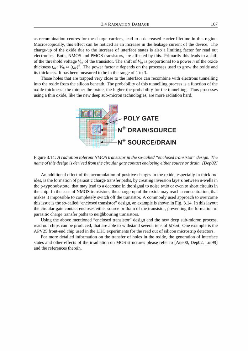
3.4 RADIATION DAMAGE 107
as recombination centres for the charge carriers, lead to a decreased carrier lifetime in this region.Macroscopically, this effect can be noticed as an increase in the leakage current of the device. Thecharge-up of the oxide due to the increase of interface states is also a limiting factor for read outelectronics. Both, NMOS and PMOS transistors, are affected by this. Primarily this leads to a shiftof the threshold voltage Vth of the transistor. The shift of Vth is proportional to a power n of the oxidethickness tox: Vth ∝ (tox)
n. The power factor n depends on the processes used to grow the oxide andits thickness. It has been measured to be in the range of 1 to 3.
Those holes that are trapped very close to the interface can recombine with electrons tunnellinginto the oxide from the silicon beneath. The probability of this tunnelling process is a function of theoxide thickness: the thinner the oxide, the higher the probability for the tunnelling. Thus processesusing a thin oxide, like the new deep sub-micron technologies, are more radiation hard.
Figure 3.14: A radiation tolerant NMOS transistor in the so-called “enclosed transistor” design. Thename of this design is derived from the circular gate contact enclosing either source or drain. [Dep02]
An additional effect of the accumulation of positive charges in the oxide, especially in thick ox-ides, is the formation of parasitic charge transfer paths, by creating inversion layers between n-wells inthe p-type substrate, that may lead to a decrease in the signal to noise ratio or even to short circuits inthe chip. In the case of NMOS transistors, the charge-up of the oxide may reach a concentration, thatmakes it impossible to completely switch off the transistor. A commonly used approach to overcomethis issue is the so-called “enclosed transistor” design, an example is shown in Fig. 3.14. In this layoutthe circular gate contact encloses either source or drain of the transistor, preventing the formation ofparasitic charge transfer paths to neighbouring transistors.
Using the above mentioned “enclosed transistor” design and the new deep sub-micron process,read out chips can be produced, that are able to withstand several tens of Mrad. One example is theAPV25 front-end chip used in the LHC experiments for the read out of silicon microstrip detectors.
For more detailed information on the transfer of holes in the oxide, the generation of interfacestates and other effects of the irradiation on MOS structures please refer to [Ane00, Dep02, Lut99]and the references therein.


Chapter 4
Medical Radiation Imaging
Ever since Wilhelm Conrad Rontgen took the first X-ray image of his wife’s hand in 1895, radiationhas become more and more important in medicine, both in diagnostics and in treatment. After thefirst enthusiastic years, it soon became obvious that a thorough dosimetry had to go hand in hand withevery application of radiation. Today’s state of the art detectors and electronics cover an enormousfield of dosimetry and imaging applications, from in-vivo dosimetry to digital X-ray systems.
The goal of the SUCIMA project was to transfer know-how from the HEP community to medicalapplications, namely dosimetry of extended sources and online beam monitoring. In the followingsections the project itself will be introduced together with its two main applications and the require-ments on the sensors resulting from these, as well as the sensors developed within this project.
4.1 SUCIMA
SUCIMA(1) is a project, supported by the European Commission within the Fifth Framework Pro-gramme (contract no. G1RD-CT-2001-00561), addressing the development of an imaging techniqueof extended radioactive sources based on monolithic and hybrid position sensitive silicon sensors,where “imaging” has to be understood as the record of a dose map. The detector characteristics areconstrained by the two main applications, namely intravascular brachytherapy and real time monitor-ing of a proton beam for oncology.
The SUCIMA collaboration consists of eleven partners from five European countries. Amongthese partners are not only universities, but also four research centres and two companies.
4.1.1 Intravascular Brachytherapy
Brachytherapy is the medical term describing a radiation treatment in which a radioactive source isbrought close to the target volume. The name “brachy” is derived from the Greek “brakhus”, whichtranslates as “short” or “close by”.
Originally, Brachytherapy is an oncological treatment, in which the radiation is used to destroythe DNA of malignant cells to prevent further growth of the tissue. The applications range frompermanent implantation of low-activity, short half-life time seeds (e.g. 125I or 103Pd) when treatingprostate cancer to short term insertions of high-activity sources (e.g. 192Ir) when treating laryngealcancer. The second type of brachytherapy is also called afterloading.
In recent years a second field became more and more important for the Brachytherapy: coronaryartery diseases (CAD). CAD are often linked to an artery narrowing (stenosis). This narrowing, causedby the build-up of plaque, will lead to an oxygen lack in the heart muscle which in turn increases therisk of a heart attack. There are two possible treatments for this: surgery, a bypass to the blocked
(1)SUCIMA: Silicon Ultra fast Cameras for electron and gamma sources In Medical Applications
109
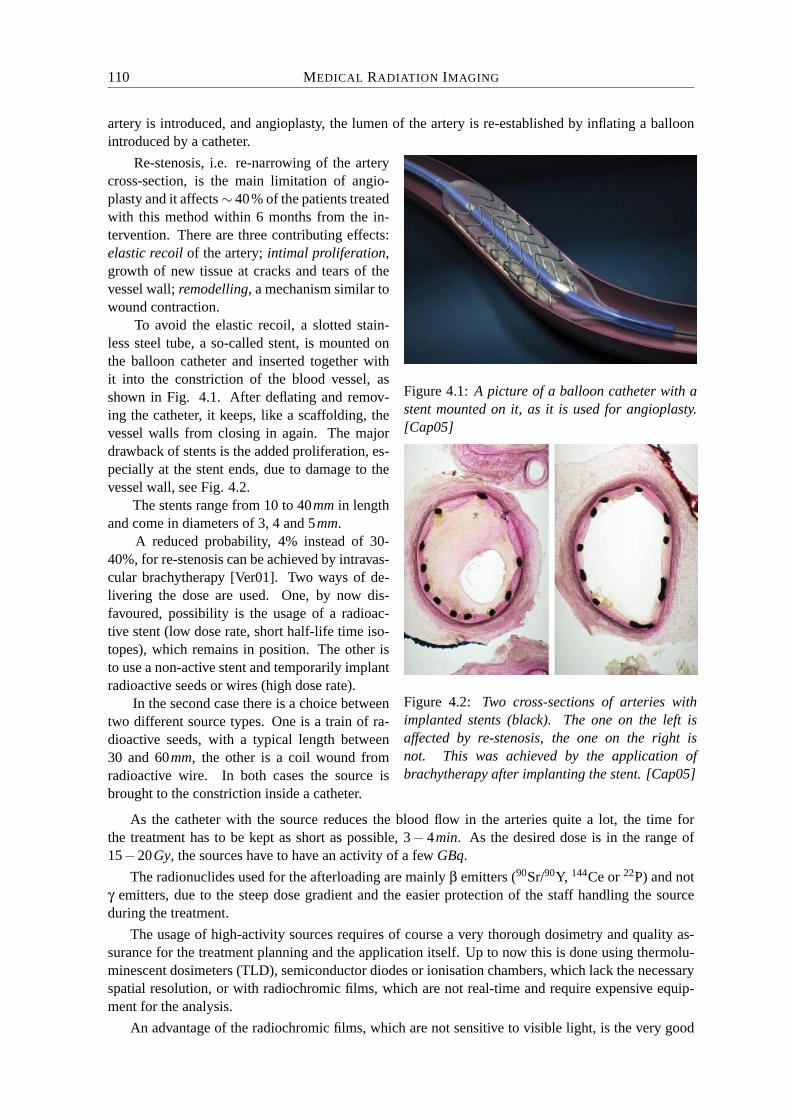
110 MEDICAL RADIATION IMAGING
artery is introduced, and angioplasty, the lumen of the artery is re-established by inflating a balloonintroduced by a catheter.
Re-stenosis, i.e. re-narrowing of the arterycross-section, is the main limitation of angio-plasty and it affects ∼ 40% of the patients treatedwith this method within 6 months from the in-tervention. There are three contributing effects:elastic recoil of the artery; intimal proliferation,growth of new tissue at cracks and tears of thevessel wall; remodelling, a mechanism similar towound contraction.
To avoid the elastic recoil, a slotted stain-less steel tube, a so-called stent, is mounted onthe balloon catheter and inserted together withit into the constriction of the blood vessel, asshown in Fig. 4.1. After deflating and remov-ing the catheter, it keeps, like a scaffolding, thevessel walls from closing in again. The majordrawback of stents is the added proliferation, es-pecially at the stent ends, due to damage to thevessel wall, see Fig. 4.2.
The stents range from 10 to 40mm in lengthand come in diameters of 3, 4 and 5mm.
A reduced probability, 4% instead of 30-40%, for re-stenosis can be achieved by intravas-cular brachytherapy [Ver01]. Two ways of de-livering the dose are used. One, by now dis-favoured, possibility is the usage of a radioac-tive stent (low dose rate, short half-life time iso-topes), which remains in position. The other isto use a non-active stent and temporarily implantradioactive seeds or wires (high dose rate).
In the second case there is a choice betweentwo different source types. One is a train of ra-dioactive seeds, with a typical length between30 and 60mm, the other is a coil wound fromradioactive wire. In both cases the source isbrought to the constriction inside a catheter.
Figure 4.1: A picture of a balloon catheter with astent mounted on it, as it is used for angioplasty.[Cap05]
Figure 4.2: Two cross-sections of arteries withimplanted stents (black). The one on the left isaffected by re-stenosis, the one on the right isnot. This was achieved by the application ofbrachytherapy after implanting the stent. [Cap05]
As the catheter with the source reduces the blood flow in the arteries quite a lot, the time forthe treatment has to be kept as short as possible, 3− 4min. As the desired dose is in the range of15−20Gy, the sources have to have an activity of a few GBq.
The radionuclides used for the afterloading are mainly β emitters (90Sr/90Y, 144Ce or 22P) and notγ emitters, due to the steep dose gradient and the easier protection of the staff handling the sourceduring the treatment.
The usage of high-activity sources requires of course a very thorough dosimetry and quality as-surance for the treatment planning and the application itself. Up to now this is done using thermolu-minescent dosimeters (TLD), semiconductor diodes or ionisation chambers, which lack the necessaryspatial resolution, or with radiochromic films, which are not real-time and require expensive equip-ment for the analysis.
An advantage of the radiochromic films, which are not sensitive to visible light, is the very good

4.1 SUCIMA 111
linearity over many orders of magnitude of dose (0.1−400Gy). These films consist of photomonomermolecules which change colour due to chemical changes induced by the absorbed dose, a process thatrequires many hours. A further advantage of the material is, that it is tissue equivalent and thus can beeasily used in phantoms.
The SUCIMA collaboration aims to build cameras allowing for real-time imaging of brachyther-apy sources during production and everyday usage at hospitals. To be competitive with existingdosimeters the following requirements have to be met:
• Size: In order to be able to measure the seed trains, which can be up to 60mm long, in one gothe sensor has be at least 30×70mm2.
• Granularity: The granularity of the dosimeter has to be below 50µm, to allow a precise planningof the treatment and an exact measurement of the dimensions of the source.
• Radiation Hardness: The dosimeter has to able to withstand a dose rate of 2− 20rad/s for anextended time frame.
• Sensitivity: The sensor should be able to detect single low energetic particles, but it should alsobe able to cope with 1−10 MIPs/(pixel×100µs)(2).
The efforts of the collaboration will allow for improvement of the quality control of brachytherapysources, but also for better simulations, treatment planning and customised sources. Another benefitof this will be higher safety conditions for patients and personnel.
4.1.2 Hadron Therapy
A second field of work for the collaboration is a beam monitor for hadron therapy. This device isbeing developed together with the Hadron Therapy Centre, of which TERA(3) [Ama93] is a part ofSUCIMA.
In cancer treatment, radiotherapy with X-ray or electron beams is used in ∼ 50% of the cases inaddition to chemotherapy and/or surgery. The energy released by the beam in the tissue destroys thegenetic material, mostly by creating single strand breaks (SSB), of the tumour cells and thus preventsthem from growing further.
One of the major features of the X-ray and electron beams is the exponential depth-dose curve,see Fig. 4.3. The further the beam goes into the tissue, the less intensity is left. This, together withthe problem, that the beam is not stopped in the tumour but passes on, leads to serious issues for theprotection of the healthy tissue around the tumour and results in complicated treatment plans for alarge number of cases.
Beams of protons or light ions have many advantages over the conventional treatment techniques.The first and most important is the stopping behaviour of hadrons: They deposit almost all their energywhen they reach the end of the penetration range in the so-called Bragg peak. The penetration rangestrongly depends on the energy of the incident particles. A second advantage is, that the hadrons arecharged particles: The beam can be focused and steered using magnets in the beam line.
(2)MIP: Minimum Ionising Particle, more information can be found in section 3.1 on page 89(3)TERA: TErapia con Radiazioni Adroniche, Therapy with Hadronic Radiations
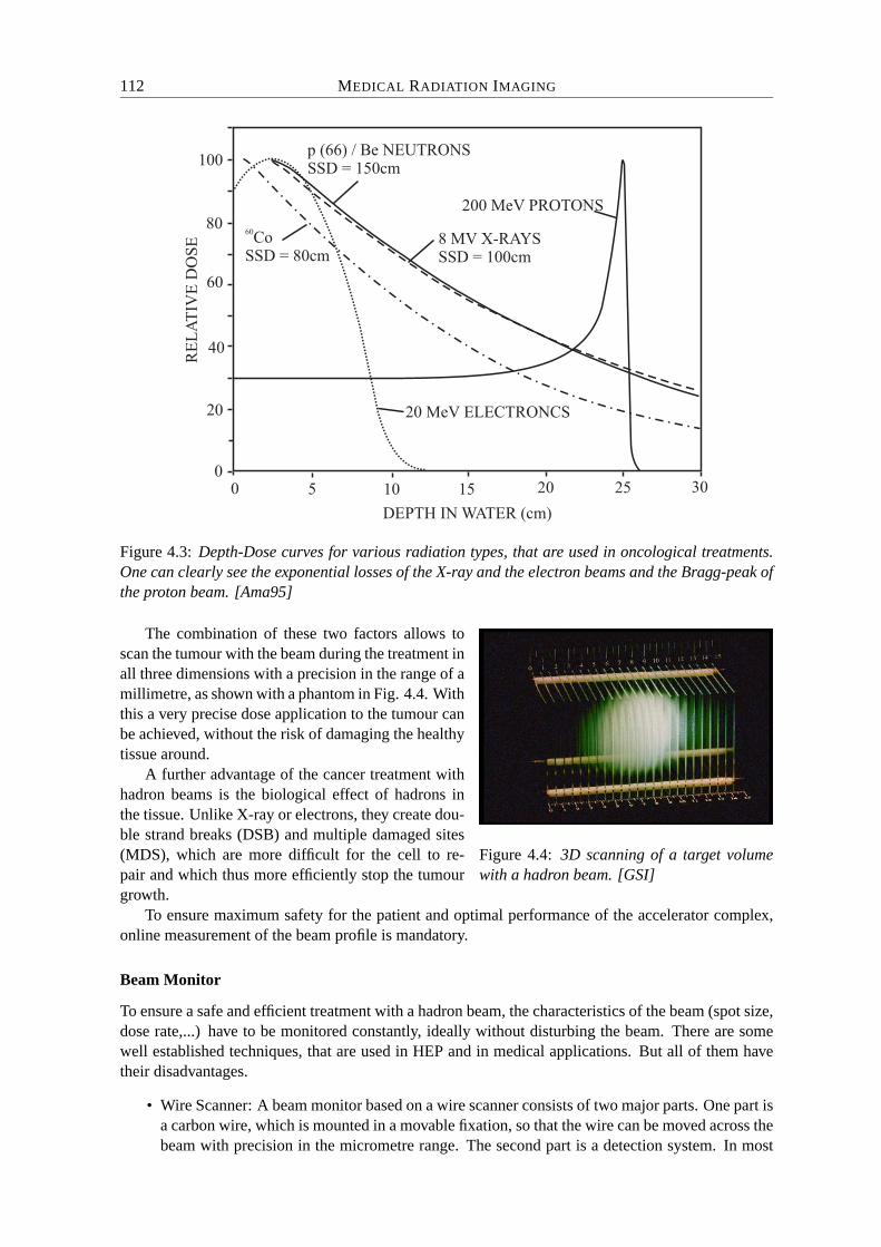
112 MEDICAL RADIATION IMAGING
100
80
60
40
20
00 5 10 15 20 25 30
DEPTH IN WATER (cm)
RE
LA
TIV
ED
OS
E
p (66) / Be NEUTRONSSSD = 150cm
60Co
SSD = 80cm
20 MeV ELECTRONCS
8 MV X-RAYSSSD = 100cm
200 MeV PROTONS
Figure 4.3: Depth-Dose curves for various radiation types, that are used in oncological treatments.One can clearly see the exponential losses of the X-ray and the electron beams and the Bragg-peak ofthe proton beam. [Ama95]
Figure 4.4: 3D scanning of a target volumewith a hadron beam. [GSI]
The combination of these two factors allows toscan the tumour with the beam during the treatment inall three dimensions with a precision in the range of amillimetre, as shown with a phantom in Fig. 4.4. Withthis a very precise dose application to the tumour canbe achieved, without the risk of damaging the healthytissue around.
A further advantage of the cancer treatment withhadron beams is the biological effect of hadrons inthe tissue. Unlike X-ray or electrons, they create dou-ble strand breaks (DSB) and multiple damaged sites(MDS), which are more difficult for the cell to re-pair and which thus more efficiently stop the tumourgrowth.
To ensure maximum safety for the patient and optimal performance of the accelerator complex,online measurement of the beam profile is mandatory.
Beam Monitor
To ensure a safe and efficient treatment with a hadron beam, the characteristics of the beam (spot size,dose rate,...) have to be monitored constantly, ideally without disturbing the beam. There are somewell established techniques, that are used in HEP and in medical applications. But all of them havetheir disadvantages.
• Wire Scanner: A beam monitor based on a wire scanner consists of two major parts. One part isa carbon wire, which is mounted in a movable fixation, so that the wire can be moved across thebeam with precision in the micrometre range. The second part is a detection system. In most
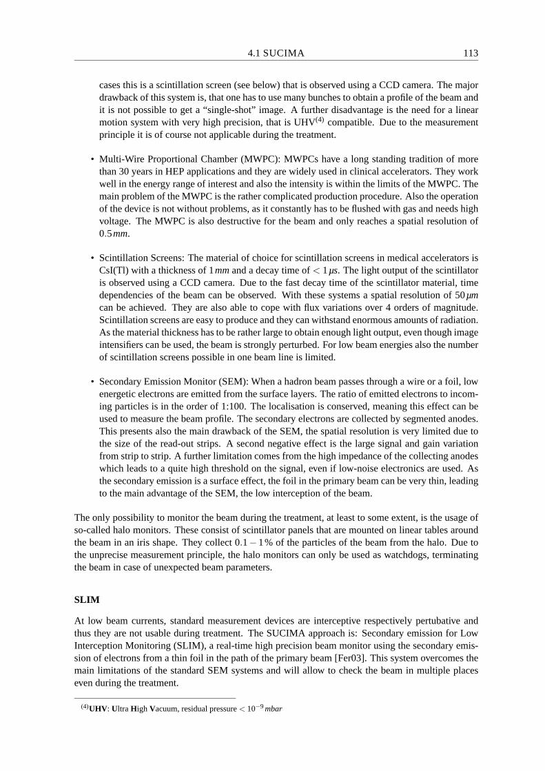
4.1 SUCIMA 113
cases this is a scintillation screen (see below) that is observed using a CCD camera. The majordrawback of this system is, that one has to use many bunches to obtain a profile of the beam andit is not possible to get a “single-shot” image. A further disadvantage is the need for a linearmotion system with very high precision, that is UHV(4) compatible. Due to the measurementprinciple it is of course not applicable during the treatment.
• Multi-Wire Proportional Chamber (MWPC): MWPCs have a long standing tradition of morethan 30 years in HEP applications and they are widely used in clinical accelerators. They workwell in the energy range of interest and also the intensity is within the limits of the MWPC. Themain problem of the MWPC is the rather complicated production procedure. Also the operationof the device is not without problems, as it constantly has to be flushed with gas and needs highvoltage. The MWPC is also destructive for the beam and only reaches a spatial resolution of0.5mm.
• Scintillation Screens: The material of choice for scintillation screens in medical accelerators isCsI(Tl) with a thickness of 1mm and a decay time of < 1µs. The light output of the scintillatoris observed using a CCD camera. Due to the fast decay time of the scintillator material, timedependencies of the beam can be observed. With these systems a spatial resolution of 50µmcan be achieved. They are also able to cope with flux variations over 4 orders of magnitude.Scintillation screens are easy to produce and they can withstand enormous amounts of radiation.As the material thickness has to be rather large to obtain enough light output, even though imageintensifiers can be used, the beam is strongly perturbed. For low beam energies also the numberof scintillation screens possible in one beam line is limited.
• Secondary Emission Monitor (SEM): When a hadron beam passes through a wire or a foil, lowenergetic electrons are emitted from the surface layers. The ratio of emitted electrons to incom-ing particles is in the order of 1:100. The localisation is conserved, meaning this effect can beused to measure the beam profile. The secondary electrons are collected by segmented anodes.This presents also the main drawback of the SEM, the spatial resolution is very limited due tothe size of the read-out strips. A second negative effect is the large signal and gain variationfrom strip to strip. A further limitation comes from the high impedance of the collecting anodeswhich leads to a quite high threshold on the signal, even if low-noise electronics are used. Asthe secondary emission is a surface effect, the foil in the primary beam can be very thin, leadingto the main advantage of the SEM, the low interception of the beam.
The only possibility to monitor the beam during the treatment, at least to some extent, is the usage ofso-called halo monitors. These consist of scintillator panels that are mounted on linear tables aroundthe beam in an iris shape. They collect 0.1− 1% of the particles of the beam from the halo. Due tothe unprecise measurement principle, the halo monitors can only be used as watchdogs, terminatingthe beam in case of unexpected beam parameters.
SLIM
At low beam currents, standard measurement devices are interceptive respectively pertubative andthus they are not usable during treatment. The SUCIMA approach is: Secondary emission for LowInterception Monitoring (SLIM), a real-time high precision beam monitor using the secondary emis-sion of electrons from a thin foil in the path of the primary beam [Fer03]. This system overcomes themain limitations of the standard SEM systems and will allow to check the beam in multiple placeseven during the treatment.
(4)UHV: Ultra High Vacuum, residual pressure < 10−9 mbar
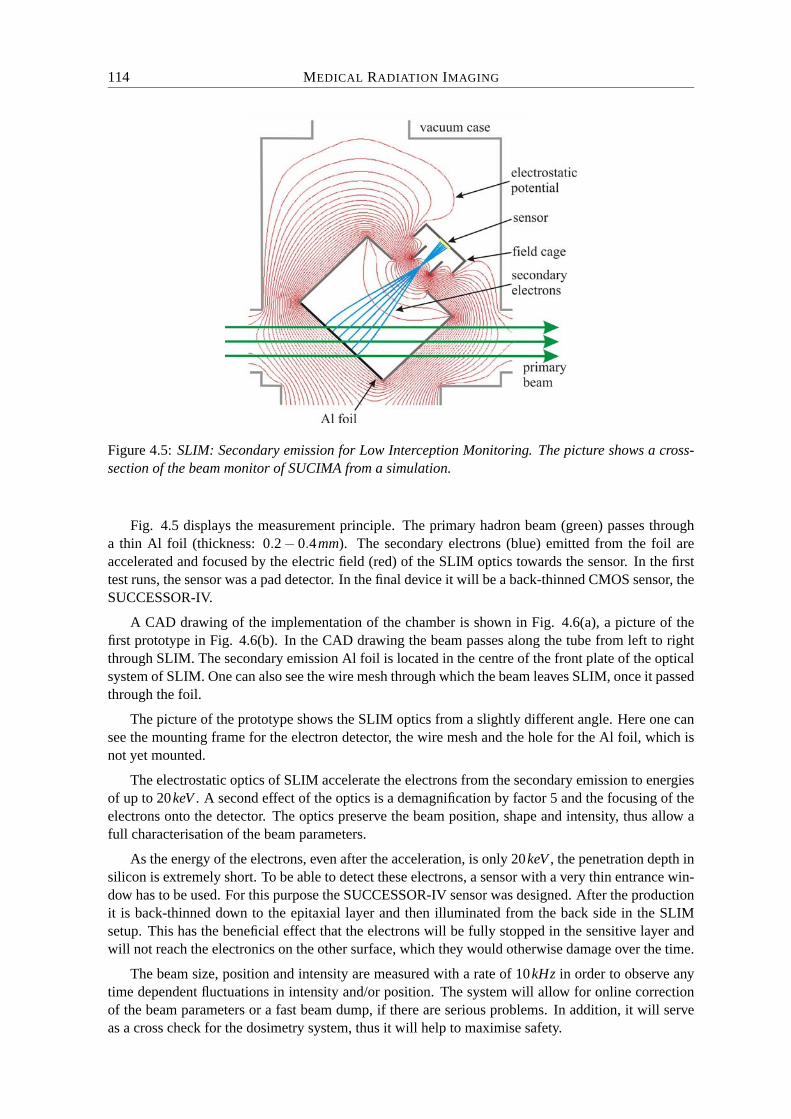
114 MEDICAL RADIATION IMAGING
Figure 4.5: SLIM: Secondary emission for Low Interception Monitoring. The picture shows a cross-section of the beam monitor of SUCIMA from a simulation.
Fig. 4.5 displays the measurement principle. The primary hadron beam (green) passes througha thin Al foil (thickness: 0.2− 0.4mm). The secondary electrons (blue) emitted from the foil areaccelerated and focused by the electric field (red) of the SLIM optics towards the sensor. In the firsttest runs, the sensor was a pad detector. In the final device it will be a back-thinned CMOS sensor, theSUCCESSOR-IV.
A CAD drawing of the implementation of the chamber is shown in Fig. 4.6(a), a picture of thefirst prototype in Fig. 4.6(b). In the CAD drawing the beam passes along the tube from left to rightthrough SLIM. The secondary emission Al foil is located in the centre of the front plate of the opticalsystem of SLIM. One can also see the wire mesh through which the beam leaves SLIM, once it passedthrough the foil.
The picture of the prototype shows the SLIM optics from a slightly different angle. Here one cansee the mounting frame for the electron detector, the wire mesh and the hole for the Al foil, which isnot yet mounted.
The electrostatic optics of SLIM accelerate the electrons from the secondary emission to energiesof up to 20keV . A second effect of the optics is a demagnification by factor 5 and the focusing of theelectrons onto the detector. The optics preserve the beam position, shape and intensity, thus allow afull characterisation of the beam parameters.
As the energy of the electrons, even after the acceleration, is only 20keV , the penetration depth insilicon is extremely short. To be able to detect these electrons, a sensor with a very thin entrance win-dow has to be used. For this purpose the SUCCESSOR-IV sensor was designed. After the productionit is back-thinned down to the epitaxial layer and then illuminated from the back side in the SLIMsetup. This has the beneficial effect that the electrons will be fully stopped in the sensitive layer andwill not reach the electronics on the other surface, which they would otherwise damage over the time.
The beam size, position and intensity are measured with a rate of 10kHz in order to observe anytime dependent fluctuations in intensity and/or position. The system will allow for online correctionof the beam parameters or a fast beam dump, if there are serious problems. In addition, it will serveas a cross check for the dosimetry system, thus it will help to maximise safety.

4.1 SUCIMA 115
(a) CAD Drawing (b) Prototype
Figure 4.6: The Implementation of the SLIM system. (a) shows a CAD drawing. The aluminum foil islocated in the centre of the front plate of the optical system. Also visible is the mesh grid in the side ofthe optical system through which the beam exits. In (b) the optical system of the prototype is depictedfrom the reverse angle compared to (a). Source: SUCIMA Collaboration.
In order to fulfil the requirements for a fast and precise beam monitor (uncertainty in the delivereddose < 2.5%) for medical applications, the sensor has to meet the following standards:
• Size: The primary beam has a diameter of a few centimetres before entering the quadrupolemagnet focusing it into the target. Even with the demagnification of the focal system the size ofthe sensor still has to be larger than 15×15mm2.
• Granularity: The requirements on the granularity of the sensor are not as high as for the dosime-try: 200µm
• Radiation Hardness: Radiation hardness is not an issue in this application, as the low energeticelectrons (20keV ) are all fully stopped in the sensitive layer of the detector and do not reach theelectronics layer, which they might damage over time.
• Sensitivity: The low energy of the secondary electrons, even after the acceleration, is somewhatof an issue, but this can be overcome by using back-thinned CMOS sensors, which have anegligible dead layer. The dynamical range, a sensor has to be able to cope with, is 0.2−2000MIP/(pixel×100µs).
• Speed: As time dependent phenomena of the beam should be detected by the system, the framerate has to be at least 10000 f ps(5).
4.1.3 SUCIMA – Summary Detector Specifications
Specification Brachytherapy Hadron Therapy
Size [mm2] 30×60, stitched 15×15Granularity [µm] 50 200Rad. Dose [rad/s] 2−20 0Sensitivity [MIPs/(pixel×100µs)] 1−10 0.2−2000Speed [fps] 10-100 10000
Table 4.1: This table summarises the requirements on the detectors for the two applications ofSUCIMA, brachytherapy and hadron therapy.
(5)fps: frames per second

116 MEDICAL RADIATION IMAGING
4.2 SUCIMA Medical Detectors
In the SUCIMA project a variety of sensors has been used for different applications. This chapter willgive an introduction to the sensors themselves and to the read out electronics developed within theSUCIMA collaboration.
The main purpose of radiation sensors in medical applications are either imaging, e.g. radio-graphy, or quality control of treatment procedures. The sensors used up to now are either very slow(GAFchromic films) or have a very poor spatial resolution (ionisation chambers). Also most of thesystems are very expensive.
The approach of SUCIMA to use state-of-the-art silicon devices for some very specific applica-tions allows to combine high granularity with fast acquisition times. The devices are cross-calibratedagainst well established systems to ensure the conformity with medical regulations.
There are many silicon devices that can be used as detectors for radiation. There are some tech-nologies that have been used in High Energy Physics for decades, but also some interesting newdevelopments. SUCIMA concentrated its efforts on three of these technologies: Silicon Micro-StripDetectors, CMOS(6) pixel sensors and SOI(7) pixel sensors.
In the following sections the sensors designed and/or used by the SUCIMA will be introduced,with the emphasis on the CMOS pixel detectors. A detailed insight into the various developmentstages and prototypes will be given on that matter, while the silicon micro-strip and the SOI detectorswill only be shortly introduced.
4.2.1 Silicon Micro-Strip Detectors
Silicon micro-strip sensors have a long-standing tradition in High Energy Physics. They have beensuccessfully used for many years in large scale experiments like DELPHI(8) [Cho98] or CDF(9) [Sil00]and will be used in even bigger experiments like CMS(10) [Kra04].
As the development from scratch and the production of a silicon micro-strip detector is time con-suming and expensive, SUCIMA chose to use off-the-shelf components for the sensor and the read outsystem, especially since the strip detectors were only regarded as a backup in case the development ofthe pixel devices would have failed. Nevertheless, they proved to be very valuable to better understandthe requirements on the pixel sensors and for dosimetric measurements with highly active seeds.
The sensors used by SUCIMA, see Fig. 4.7, were developed for the AGILE(11) experiment [Tav03]and are produced by Hamamatsu Photonics K.K. The sensors are 9.5× 9.5cm2 large and have 768read out strips with a pitch of 121µm. The full depletion voltage is ∼ 80V with a leakage current of0.1nA per strip.
The read out system is based on a VA pre-amplifier ASIC by IDEAs ASA. The data acquisitionis either done by a VME based system or by the SUCIMA Imager, a USB2.0 read out board. Moreinformation on the SUCIMA Imager can be found in section 4.3.1 on page 126.
The strip sensors were mainly used in dosimetry setups where the dose of a radioactive source wasmeasured as a function of the radian around the catheter or the depth of a water equivalent material.
A detailed description of the silicon micro-strip sensors, the setup and their performance can befound in [Cap05].
(6)CMOS: Complementary Metal Oxide Semiconductor(7)SOI: Silicon-On-Insulator(8)DELPHI: DEtector for Lepton, Photon and Hadron Identification(9)CDF: the Collider Detector at Fermilab
(10)CMS: Compact Muon Solenoid(11)AGILE: Astro-rivelatore Gamma a Immagini LEggero
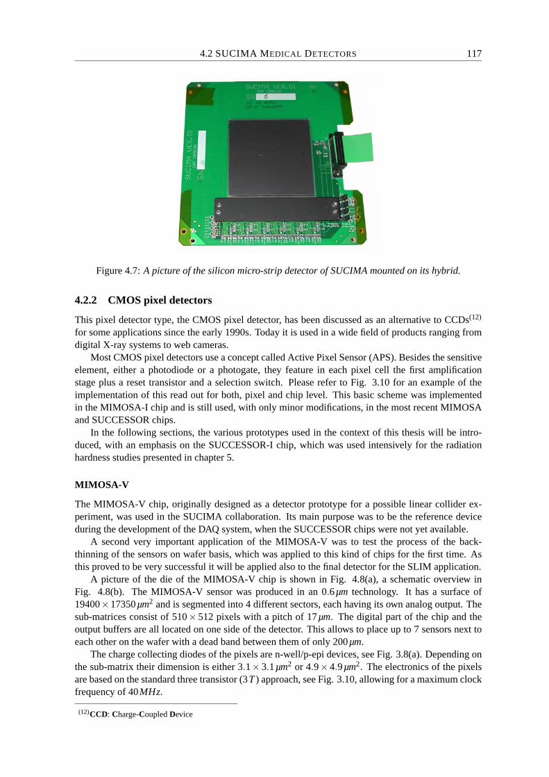
4.2 SUCIMA MEDICAL DETECTORS 117
Figure 4.7: A picture of the silicon micro-strip detector of SUCIMA mounted on its hybrid.
4.2.2 CMOS pixel detectors
This pixel detector type, the CMOS pixel detector, has been discussed as an alternative to CCDs(12)
for some applications since the early 1990s. Today it is used in a wide field of products ranging fromdigital X-ray systems to web cameras.
Most CMOS pixel detectors use a concept called Active Pixel Sensor (APS). Besides the sensitiveelement, either a photodiode or a photogate, they feature in each pixel cell the first amplificationstage plus a reset transistor and a selection switch. Please refer to Fig. 3.10 for an example of theimplementation of this read out for both, pixel and chip level. This basic scheme was implementedin the MIMOSA-I chip and is still used, with only minor modifications, in the most recent MIMOSAand SUCCESSOR chips.
In the following sections, the various prototypes used in the context of this thesis will be intro-duced, with an emphasis on the SUCCESSOR-I chip, which was used intensively for the radiationhardness studies presented in chapter 5.
MIMOSA-V
The MIMOSA-V chip, originally designed as a detector prototype for a possible linear collider ex-periment, was used in the SUCIMA collaboration. Its main purpose was to be the reference deviceduring the development of the DAQ system, when the SUCCESSOR chips were not yet available.
A second very important application of the MIMOSA-V was to test the process of the back-thinning of the sensors on wafer basis, which was applied to this kind of chips for the first time. Asthis proved to be very successful it will be applied also to the final detector for the SLIM application.
A picture of the die of the MIMOSA-V chip is shown in Fig. 4.8(a), a schematic overview inFig. 4.8(b). The MIMOSA-V sensor was produced in an 0.6µm technology. It has a surface of19400×17350µm2 and is segmented into 4 different sectors, each having its own analog output. Thesub-matrices consist of 510× 512 pixels with a pitch of 17µm. The digital part of the chip and theoutput buffers are all located on one side of the detector. This allows to place up to 7 sensors next toeach other on the wafer with a dead band between them of only 200µm.
The charge collecting diodes of the pixels are n-well/p-epi devices, see Fig. 3.8(a). Depending onthe sub-matrix their dimension is either 3.1×3.1µm2 or 4.9×4.9µm2. The electronics of the pixelsare based on the standard three transistor (3T ) approach, see Fig. 3.10, allowing for a maximum clockfrequency of 40MHz.
(12)CCD: Charge-Coupled Device

118 MEDICAL RADIATION IMAGING
(a) Die (b) Layout
Figure 4.8: (a) shows a picture of the actual die of a MIMOSA-V detector. The arrangement of thesub-matrices and the analog and digital read out parts on the sensor are depicted in (b). [Dep03a]
The MIMOSA-V offers a set of different operation modes. It can be read out in the standard way,with a rolling shutter(13) or in a so-called fast scan mode(14). In the last mode only every ninth pixel,in both directions, is read out. In order not to lose signal in this mode, the signal from the interleavedpixels can be summed.
A more detailed description of the sensor and its performance can be found in [Dep03a].
MIMOSA-V back-thinned
For the detection of low energetic particles one has to use a sensor with a very low threshold energy. Insilicon sensors this threshold is defined by the thickness of the dead layer above the sensitive volumeand the characteristic stopping power for this particle.
The thickness of the dead layer is typically in the range of a few µm, which corresponds to athreshold on the energy of a few tens of keV for electrons. The metallisation layers intrinsic to theCMOS sensors increase the problem even further.
The apparent approach to solve the issues caused by the dead layer is to flip the sensor over andshine it from the backside. Unfortunately, this does not help immediately for CMOS sensors, as theyhave a few hundred µm insensitive bulk material beneath the active layer, the epitaxial layer.
The idea is then, roughly spoken, to glue a handle wafer on top of the sensor for mechanicalstability and etch the backside down to the sensitive volume. This process will be described in moredetail in the following:
• Fig. 4.9(a) shows the CMOS pixel sensor in its standard configuration. One can immediatelysee the first problem of this process. The surface of the chips is not even. At places where thereare many interconnection layers, the sensor is higher, at the locations of the bond pads it is muchlower. Thus before glueing the handle wafer onto the sensor wafer(15), these inhomogeneitieshave to be evened out. Especially the “holes” above the bond pads have to be filled up, as thebond pads will be later on used from the other side.
(13)In the rolling shutter mode only a few rows are kept active and are read out while all others are kept at resetlevel. This set of active rows constantly moves in a cycle through the detector.
(14)This is an interleaved read out mode. Only every 81st pixel is read out (every 9th in both dimensions).(15)This has to be done on the still un-diced wafer. Previous tests had proven that back-thinning on an individual
sensor basis was not achievable.
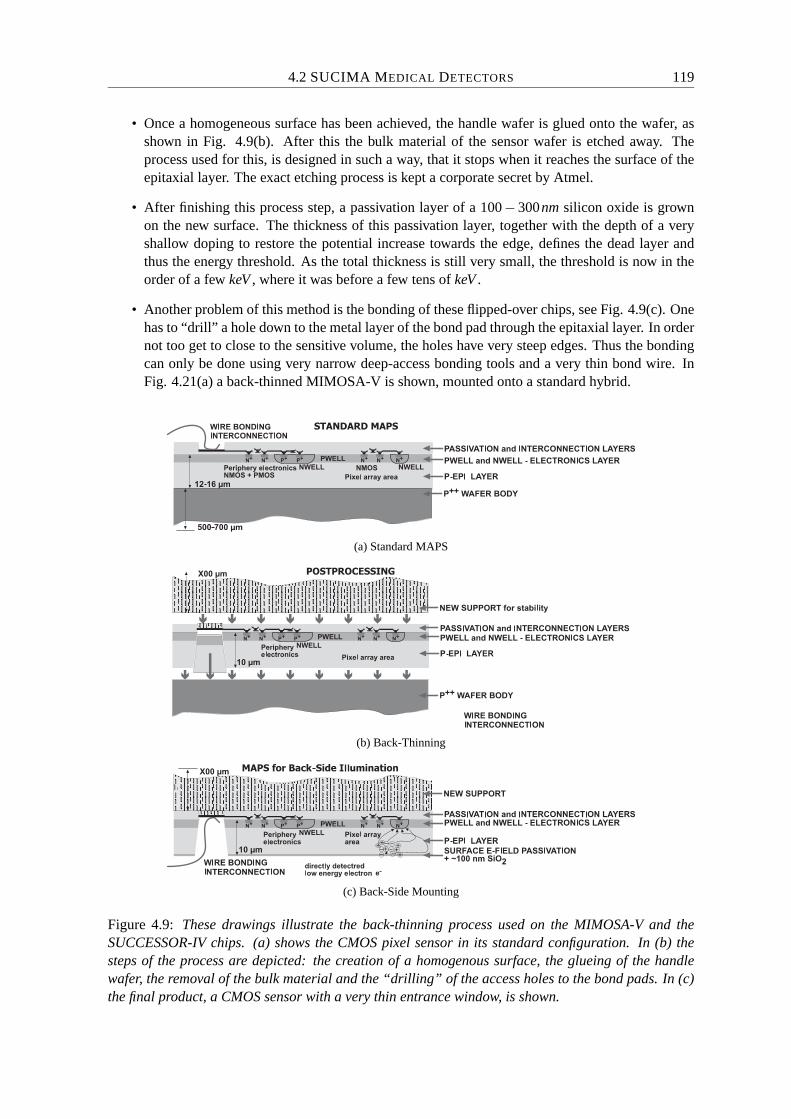
4.2 SUCIMA MEDICAL DETECTORS 119
• Once a homogeneous surface has been achieved, the handle wafer is glued onto the wafer, asshown in Fig. 4.9(b). After this the bulk material of the sensor wafer is etched away. Theprocess used for this, is designed in such a way, that it stops when it reaches the surface of theepitaxial layer. The exact etching process is kept a corporate secret by Atmel.
• After finishing this process step, a passivation layer of a 100− 300nm silicon oxide is grownon the new surface. The thickness of this passivation layer, together with the depth of a veryshallow doping to restore the potential increase towards the edge, defines the dead layer andthus the energy threshold. As the total thickness is still very small, the threshold is now in theorder of a few keV , where it was before a few tens of keV .
• Another problem of this method is the bonding of these flipped-over chips, see Fig. 4.9(c). Onehas to “drill” a hole down to the metal layer of the bond pad through the epitaxial layer. In ordernot too get to close to the sensitive volume, the holes have very steep edges. Thus the bondingcan only be done using very narrow deep-access bonding tools and a very thin bond wire. InFig. 4.21(a) a back-thinned MIMOSA-V is shown, mounted onto a standard hybrid.
(a) Standard MAPS
(b) Back-Thinning
(c) Back-Side Mounting
Figure 4.9: These drawings illustrate the back-thinning process used on the MIMOSA-V and theSUCCESSOR-IV chips. (a) shows the CMOS pixel sensor in its standard configuration. In (b) thesteps of the process are depicted: the creation of a homogenous surface, the glueing of the handlewafer, the removal of the bulk material and the “drilling” of the access holes to the bond pads. In (c)the final product, a CMOS sensor with a very thin entrance window, is shown.
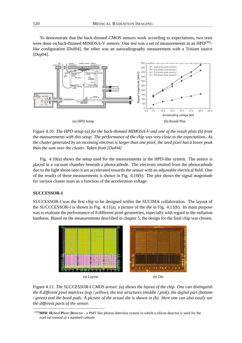
120 MEDICAL RADIATION IMAGING
To demonstrate that the back-thinned CMOS sensors work according to expectations, two testswere done on back-thinned MIMOSA-V sensors. One test was a set of measurements in an HPD(16)-like configuration [Dul04], the other was an autoradiography measurement with a Tritium source[Dep04].
(a) HPD Setup (b) Result Plot
Figure 4.10: The HPD setup (a) for the back-thinned MIMOSA-V and one of the result plots (b) fromthe measurements with this setup. The performance of the chip was very close to the expectations. Asthe cluster generated by an incoming electron is larger than one pixel, the seed pixel has a lower peakthan the sum over the cluster. Taken from [Dul04]
Fig. 4.10(a) shows the setup used for the measurements in the HPD-like system. The sensor isplaced in a vacuum chamber beneath a photocathode. The electrons emitted from the photocathodedue to the light shone onto it are accelerated towards the sensor with an adjustable electrical field. Oneof the results of these measurements is shown in Fig. 4.10(b). The plot shows the signal magnitudefor various cluster sizes as a function of the acceleration voltage.
SUCCESSOR-I
SUCCESSOR-I was the first chip to be designed within the SUCIMA collaboration. The layout ofthe SUCCCESSOR-I is shown in Fig. 4.11(a), a picture of the die in Fig. 4.11(b). Its main purposewas to evaluate the performance of 8 different pixel geometries, especially with regard to the radiationhardness. Based on the measurements described in chapter 5, the design for the final chip was chosen.
(a) Layout (b) Die
Figure 4.11: The SUCCESSOR-I CMOS sensor. (a) shows the layout of the chip. One can distinguishthe 8 different pixel matrices (top / yellow), the test structures (middle / pink), the digital part (bottom/ green) and the bond pads. A picture of the actual die is shown in (b). Here one can also easily seethe different parts of the sensor.
(16)HPD: Hybrid Photo Detector - a PMT like photon detection system in which a silicon detector is used for theread out instead of a standard cathode

4.2 SUCIMA MEDICAL DETECTORS 121
The chip was produced using the AMIS 0.35µm technology, which has a 4µm epitaxial layer.The overall dimensions of the chip are 4600× 3600µm2. As already mentioned, the chip features 8different pixel arrays, which can clearly be seen in Figs. 4.11(a) and 4.11(b). Each of them consistsof 32×32 pixels arranged in clusters of 4 pixels, the so-called super-pixels (see Fig. 4.12). The pixelpitch is 30µm for the basic pixels and 60µm for the super-pixels.
N-well (collecting diode)
N-well (guard ring)
read-out electronics
60µm
60µ
m
Figure 4.12: The so-called super-pixel of the SUCCESSOR-I. One super-pixel contains 4 pixels whichare arranged in such a way, that the read out electronics are located in the centre and can be separatedfrom the sensitive volume by a guard ring.
To increase the radiation hardness of the pixels, especially to counter the loss of charge collectionefficiency due to parasitic collection paths, source and drain of the reset transistor were swapped inthis design. Additionally, a radiation hard “enclosed” design was chosen.
The 4 channel parallel output allows to clock the chip with a maximum read out frequency of40MHz. The digital part of the chip is designed using non-radiation-tolerant standard cells. Thisrequired the use of shielding during the irradiation to protect the digital part, see section 5.2.1.
In the following each of the 8 different pixel types will be introduced briefly. A picture of eachpixel schematic is shown in Figs. 4.13 and 4.14. Their most important features are summarised in acomparison table at the end of this section.
Pixel 0: This pixel has a C-shaped collection diode, whichis rather large with ∼ 34µm2. Nevertheless, thecapacitance of the pixel, 32 f F , is only 50%larger than that of the pixels with smaller diodes.A guard ring separates the collecting diode fromthe read out electronics. Another feature of thispixel is the metal field plate on top of the junc-tion which can be biased with a negative voltage.The fill factor (definition see below) of this pixelis 85%
Pixel 1: The design of this pixel is very similar to that ofPixel 0. The collecting diode has the same size, ∼34µm2 and almost the same capacitance, 30 f F .The major difference between Pixel 1 and Pixel 0is, that Pixel 1 has no field plate on the junction.Again, the fill factor is 85%, as Pixel 1 also has aguard ring between the electronics and the diode.
Figure 4.13: Pixel Layout
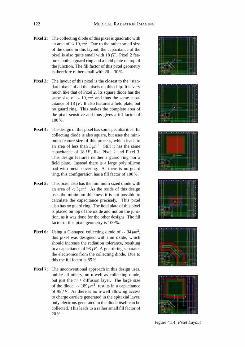
122 MEDICAL RADIATION IMAGING
Pixel 2: The collecting diode of this pixel is quadratic withan area of ∼ 10µm2. Due to the rather small sizeof the diode in this layout, the capacitance of thepixel is also quite small with 18 f F . Pixel 2 fea-tures both, a guard ring and a field plate on top ofthe junction. The fill factor of this pixel geometryis therefore rather small with 20−30%.
Pixel 3: The layout of this pixel is the closest to the “stan-dard pixel” of all the pixels on this chip. It is verymuch like that of Pixel 2. Its square diode has thesame size of ∼ 10µm2 and thus the same capa-citance of 18 f F . It also features a field plate, butno guard ring. This makes the complete area ofthe pixel sensitive and thus gives a fill factor of100%.
Pixel 4: The design of this pixel has some peculiarities. Itscollecting diode is also square, but uses the mini-mum feature size of this process, which leads toan area of less than 3µm2. Still it has the samecapacitance of 18 f F , like Pixel 2 and Pixel 3.This design features neither a guard ring nor afield plate. Instead there is a large poly siliconpad with metal covering. As there is no guardring, this configuration has a fill factor of 100%.
Pixel 5: This pixel also has the minimum sized diode withan area of < 3µm2. As the oxide of this designuses the minimum thickness it is not possible tocalculate the capacitance precisely. This pixelalso has no guard ring. The field plate of this pixelis placed on top of the oxide and not on the junc-tion, as it was done for the other designs. The fillfactor of this pixel geometry is 100%.
Pixel 6: Using a C-shaped collecting diode of ∼ 34µm2,this pixel was designed with thin oxide, whichshould increase the radiation tolerance, resultingin a capacitance of 93 f F . A guard ring separatesthe electronics from the collecting diode. Due tothis the fill factor is 85%.
Pixel 7: The unconventional approach in this design uses,unlike all others, no n-well as collecting diode,but just the n++ diffusion layer. The large sizeof the diode, ∼ 189µm2, results in a capacitanceof 95 f F . As there is no n-well allowing accessto charge carriers generated in the epitaxial layer,only electrons generated in the diode itself can becollected. This leads to a rather small fill factor of20%.
Figure 4.14: Pixel Layout

4.2 SUCIMA MEDICAL DETECTORS 123
The limitation of the fill factor, which is defined as the sensitive area divided by the total area of apixel, to a value less than 100% is mostly due to the guard ring, which acts as a competitive collectionpath and prevents charge generated beneath the read out electronics of the pixel from reaching thecollecting diode.
Pixel 0 Pixel 1 Pixel 2 Pixel 3 Pixel 4 Pixel 5 Pixel 6 Pixel 7
diode type C-shape C-shape square square square square C-shape squarediode size [µm2] 33,49 33,49 10.24 10.24 2.89 2.89 ∼34 188.88
guard ring yes yes yes no no no yes yesfield plate yes no yes yes no yes no no
total capacitance [fF] 32 30 18 18 18 ??? 93 95fill factor [%] 85 85 20-30 100 100 100 85 20
Table 4.2: This table lists the most important properties of the 8 different pixel geometries of theSUCCESSOR-I chip.
SUCCESSOR-II
The SUCCESSOR-II chip is slightly smaller than SUCCESSOR-I with a size of 3400x3600µm2. Itsschematics and a picture of the die are shown in Fig. 4.15. It is produced in the AMS 0.35µmtechnology. Instead of standard low resistivity wafers a high resistivity substrate without epitaxiallayer was used for this submission.
(a) Schematic (b) Die
Figure 4.15: Schematic view of the SUCCESSOR-II CMOS sensor.
Like its predecessor, SUCCESSOR-II features different pixel arrays, but instead of 8 differentpixel matrices it has only 4. Again each of the matrices contains 32× 32 pixels. The pitch of thepixels is 40µm.
The overall chip layout is like the one of the MIMOSA-IV prototype [Dep03b]. It uses the samegrouping of the pixel matrices and the same digital part including arrangement of the bond pads. Thedigital part is designed using radiation hard transistor layouts.
The four different pixel matrices consist of two PhotoFET pixel matrices, one self-biasing pixelmatrix and one standard pixel matrix. The main difference between the two PhotoFET matrices is,that in one of them the pixels are grouped in sub-arrays.
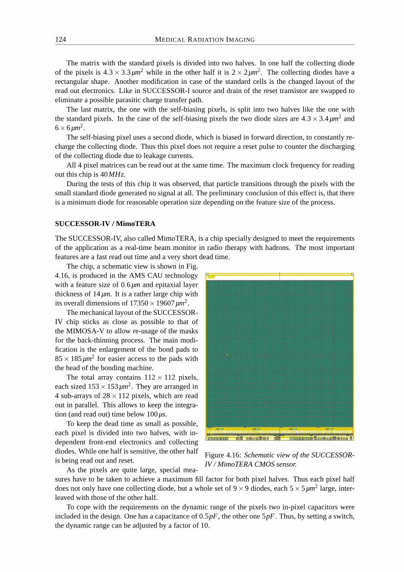
124 MEDICAL RADIATION IMAGING
The matrix with the standard pixels is divided into two halves. In one half the collecting diodeof the pixels is 4.3× 3.3µm2 while in the other half it is 2× 2µm2. The collecting diodes have arectangular shape. Another modification in case of the standard cells is the changed layout of theread out electronics. Like in SUCCESSOR-I source and drain of the reset transistor are swapped toeliminate a possible parasitic charge transfer path.
The last matrix, the one with the self-biasing pixels, is split into two halves like the one withthe standard pixels. In the case of the self-biasing pixels the two diode sizes are 4.3× 3.4µm2 and6×6µm2.
The self-biasing pixel uses a second diode, which is biased in forward direction, to constantly re-charge the collecting diode. Thus this pixel does not require a reset pulse to counter the dischargingof the collecting diode due to leakage currents.
All 4 pixel matrices can be read out at the same time. The maximum clock frequency for readingout this chip is 40MHz.
During the tests of this chip it was observed, that particle transitions through the pixels with thesmall standard diode generated no signal at all. The preliminary conclusion of this effect is, that thereis a minimum diode for reasonable operation size depending on the feature size of the process.
SUCCESSOR-IV / MimoTERA
The SUCCESSOR-IV, also called MimoTERA, is a chip specially designed to meet the requirementsof the application as a real-time beam monitor in radio therapy with hadrons. The most importantfeatures are a fast read out time and a very short dead time.
Figure 4.16: Schematic view of the SUCCESSOR-IV / MimoTERA CMOS sensor.
The chip, a schematic view is shown in Fig.4.16, is produced in the AMS CAU technologywith a feature size of 0.6µm and epitaxial layerthickness of 14µm. It is a rather large chip withits overall dimensions of 17350×19607µm2.
The mechanical layout of the SUCCESSOR-IV chip sticks as close as possible to that ofthe MIMOSA-V to allow re-usage of the masksfor the back-thinning process. The main modi-fication is the enlargement of the bond pads to85× 185µm2 for easier access to the pads withthe head of the bonding machine.
The total array contains 112 × 112 pixels,each sized 153×153µm2. They are arranged in4 sub-arrays of 28× 112 pixels, which are readout in parallel. This allows to keep the integra-tion (and read out) time below 100µs.
To keep the dead time as small as possible,each pixel is divided into two halves, with in-dependent front-end electronics and collectingdiodes. While one half is sensitive, the other halfis being read out and reset.
As the pixels are quite large, special mea-sures have to be taken to achieve a maximum fill factor for both pixel halves. Thus each pixel halfdoes not only have one collecting diode, but a whole set of 9×9 diodes, each 5×5µm2 large, inter-leaved with those of the other half.
To cope with the requirements on the dynamic range of the pixels two in-pixel capacitors wereincluded in the design. One has a capacitance of 0.5pF , the other one 5pF . Thus, by setting a switch,the dynamic range can be adjusted by a factor of 10.
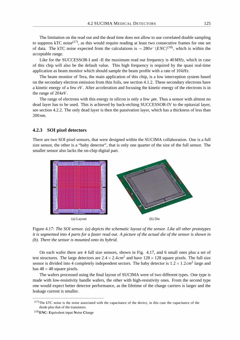
4.2 SUCIMA MEDICAL DETECTORS 125
The limitation on the read out and the dead time does not allow to use correlated double samplingto suppress kTC noise(17), as this would require reading at least two consecutive frames for one setof data. The kTC noise expected from the calculations is ∼ 280e−(ENC)(18), which is within theacceptable range.
Like for the SUCCESSOR-I and -II the maximum read out frequency is 40MHz, which in caseof this chip will also be the default value. This high frequency is required by the quasi real-timeapplication as beam monitor which should sample the beam profile with a rate of 10kHz.
The beam monitor of Tera, the main application of this chip, is a low interception system basedon the secondary electron emission from thin foils, see section 4.1.2. These secondary electrons havea kinetic energy of a few eV . After acceleration and focusing the kinetic energy of the electrons is inthe range of 20keV .
The range of electrons with this energy in silicon is only a few µm. Thus a sensor with almost nodead layer has to be used. This is achieved by back-etching SUCCESSOR-IV to the epitaxial layer,see section 4.2.2. The only dead layer is then the passivation layer, which has a thickness of less than200nm.
4.2.3 SOI pixel detectors
There are two SOI pixel sensors, that were designed within the SUCIMA collaboration. One is a fullsize sensor, the other is a “baby detector”, that is only one quarter of the size of the full sensor. Thesmaller sensor also lacks the on-chip digital part.
(a) Layout (b) Die
Figure 4.17: The SOI sensor. (a) depicts the schematic layout of the sensor. Like all other prototypesit is segmented into 4 parts for a faster read out. A picture of the actual die of the sensor is shown in(b). There the sensor is mounted onto its hybrid.
On each wafer there are 4 full size sensors, shown in Fig. 4.17, and 6 small ones plus a set oftest structures. The large detectors are 2.4×2.4cm2 and have 128×128 square pixels. The full sizesensor is divided into 4 completely independent sectors. The baby detector is 1.2×1.2cm2 large andhas 48×48 square pixels.
The wafers processed using the final layout of SUCIMA were of two different types. One type ismade with low-resistivity handle wafers, the other with high-resistivity ones. From the second typeone would expect better detector performance, as the lifetime of the charge carriers is larger and theleakage current is smaller.
(17)The kTC noise is the noise associated with the capacitance of the device, in this case the capacitance of thediode plus that of the transistors.
(18)ENC: Equivalent input Noise Charge
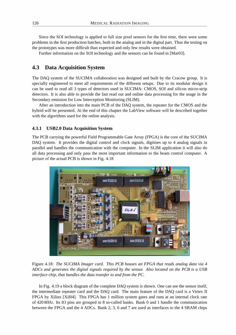
126 MEDICAL RADIATION IMAGING
Since the SOI technology is applied to full size pixel sensors for the first time, there were someproblems in the first production batches, both in the analog and in the digital part. Thus the testing onthe prototypes was more difficult than expected and only few results were obtained.
Further information on the SOI technology and the sensors can be found in [Mar03].
4.3 Data Acquisition System
The DAQ system of the SUCIMA collaboration was designed and built by the Cracow group. It isspecially engineered to meet all requirements of the different setups. Due to its modular design itcan be used to read all 3 types of detectors used in SUCIMA: CMOS, SOI and silicon micro-stripdetectors. It is also able to provide the fast read out and online data processing for the usage in theSecondary emission for Low Interception Monitoring (SLIM).
After an introduction into the main PCB of the DAQ system, the repeater for the CMOS and thehybrid will be presented. At the end of this chapter the LabView software will be described togetherwith the algorithms used for the online analysis.
4.3.1 USB2.0 Data Acquisition System
The PCB carrying the powerful Field Programmable Gate Array (FPGA) is the core of the SUCIMADAQ system. It provides the digital control and clock signals, digitises up to 4 analog signals inparallel and handles the communication with the computer. In the SLIM application it will also doall data processing and only pass the most important information to the beam control computer. Apicture of the actual PCB is shown in Fig. 4.18
Figure 4.18: The SUCIMA Imager card. This PCB houses an FPGA that reads analog data via 4ADCs and generates the digital signals required by the sensor. Also located on the PCB is a USBinterface chip, that handles the data transfer to and from the PC.
In Fig. 4.19 a block diagram of the complete DAQ system is shown. One can see the sensor itself,the intermediate repeater card and the DAQ card. The main feature of the DAQ card is a Virtex IIFPGA by Xilinx [Xil04]. This FPGA has 1 million system gates and runs at an internal clock rateof 420MHz. Its IO pins are grouped in 8 so-called banks. Bank 0 and 1 handle the communicationbetween the FPGA and the 4 ADCs. Bank 2, 3, 6 and 7 are used as interfaces to the 4 SRAM chips
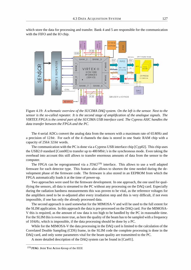
4.3 DATA ACQUISITION SYSTEM 127
which store the data for processing and transfer. Bank 4 and 5 are responsible for the communicationwith the FIFO and the IO chip.
Figure 4.19: A schematic overview of the SUCIMA DAQ system. On the left is the sensor. Next to thesensor is the so-called repeater. It is the second stage of amplification of the analogue signals. TheVIRTEX FPGA is the central part of the SUCIMA USB interface card. The Cypress ASIC handles thedata transfer between the FPGA and the PC.
The 4 serial ADCs convert the analog data from the sensors with a maximum rate of 65MHz anda precision of 12bit. For each of the 4 channels the data is stored in one Static RAM chip with acapacity of 256k 32bit words.
The communication with the PC is done via a Cypress USB interface chip [Cyp02]. This chip usesthe USB2.0 standard [Com00] to transfer up to 480Mbit/s in the synchronous mode. Even taking theoverhead into account this still allows to transfer enormous amounts of data from the sensor to thecomputer.
The FPGA can be reprogrammed via a JTAG(19) interface. This allows to use a well adaptedfirmware for each detector type. This feature also allows to shorten the time needed during the de-velopment phase of the firmware code. The firmware is also stored in an EEPROM from which theFPGA automatically loads it at the time of power-up.
Two approaches were used for the firmware development. In one approach, the one used for qual-ifying the sensors, all data is streamed to the PC without any processing on the DAQ card. Especiallyduring the radiation hardness measurements this was proven to be vital, as the reference voltages forthe amplifiers need to be re-adjusted after every irradiation step and this is very difficult, if not evenimpossible, if one has only the already processed data.
The second approach is used somewhat for the MIMOSA-V and will be used to the full extent forthe SLIM application. In this approach the data is pre-processed on the DAQ card. For the MIMOSA-V this is required, as the amount of raw data is too high to be handled by the PC in reasonable time.For the SLIM this is even more true, as here the quality of the beam has to be sampled with a frequencyof 10kHz, which is impossible, if the data processing should be done by a PC.
While for the MIMOSA-V the data processing in the DAQ card is limited to the calculation of theCorrelated Double Sampling (CDS) frame, in the SLIM code the complete processing is done in theDAQ card, and only some parameters vital for the beam quality are transmitted to the PC.
A more detailed description of the DAQ system can be found in [Cze01].
(19)JTAG: Joint Test Action Group of the IEEE

128 MEDICAL RADIATION IMAGING
4.3.2 Repeater
The repeater acts as a detector specific interface between the multi-purpose USB2.0 DAQ card andthe hybrid, which carries the sensor itself. Fig. 4.20 shows the repeater for the CMOS sensors. It ismounted as a piggy back board onto the DAQ card.
The repeater has three main functionalities in the case of the CMOS sensors. It supplies the hybridand the DAQ with power, generates the reference voltages for the amplifiers in the sensor itself andamplifies the analog signals coming from the hybrid.
The repeater is connected to 3 different voltages. From a 8.5V line all internal voltages aregenerated using standard LM317 regulators. This 8.5V line is also connected to the DAQ card, whichhas its own regulators. The other two voltages, −1.5V and −18V , are directly connected to the cableto the hybrid. They are used to apply a bias on some of the structures on the SUCCESSOR-I sensor.
The reference voltages for the amplifiers inside the sensor can be set separately for each of thefour output channels. This can be done by adjusting potentiometers in voltage dividers at the input ofoperation amplifiers. These then generate the reference voltage.
The connections to the DAQ card are established in two different ways. The power connectionsto and the digital control from the DAQ card are routed through standard pin connectors directly fromPCB to PCB. The fast digital signals, clock and reset, to and the analog signals from the sensor arerouted through very short twisted pair CAT5e cables using RJ45 connectors.
Figure 4.20: The repeater for the SUCIMA Imager. One can see the two connectors for the fastanalogue and the digital signals (top and left side), the connection to the hybrid (ribbon cable at thebottom) and the power input (on the right). The digital control signals and the power lines are routedthrough the interconnection pins. An additional connection allows to apply a negative bias to theoxide for some of the pixels.
The hybrid of the detector is connected via a 50pin ribbon cable to the repeater. This cable carriesall supply and reference voltages, as well as all digital and analog signals. To minimise the requiredspace a high density connector is used.
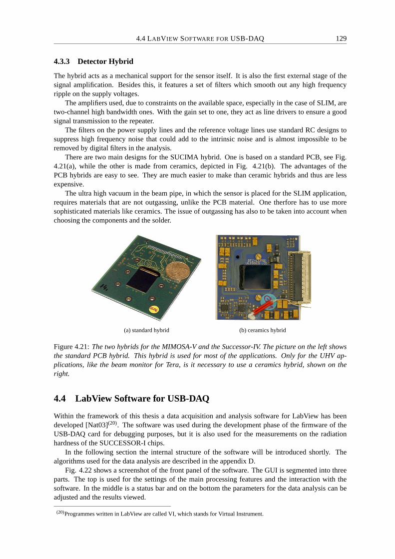
4.4 LABVIEW SOFTWARE FOR USB-DAQ 129
4.3.3 Detector Hybrid
The hybrid acts as a mechanical support for the sensor itself. It is also the first external stage of thesignal amplification. Besides this, it features a set of filters which smooth out any high frequencyripple on the supply voltages.
The amplifiers used, due to constraints on the available space, especially in the case of SLIM, aretwo-channel high bandwidth ones. With the gain set to one, they act as line drivers to ensure a goodsignal transmission to the repeater.
The filters on the power supply lines and the reference voltage lines use standard RC designs tosuppress high frequency noise that could add to the intrinsic noise and is almost impossible to beremoved by digital filters in the analysis.
There are two main designs for the SUCIMA hybrid. One is based on a standard PCB, see Fig.4.21(a), while the other is made from ceramics, depicted in Fig. 4.21(b). The advantages of thePCB hybrids are easy to see. They are much easier to make than ceramic hybrids and thus are lessexpensive.
The ultra high vacuum in the beam pipe, in which the sensor is placed for the SLIM application,requires materials that are not outgassing, unlike the PCB material. One therfore has to use moresophisticated materials like ceramics. The issue of outgassing has also to be taken into account whenchoosing the components and the solder.
(a) standard hybrid (b) ceramics hybrid
Figure 4.21: The two hybrids for the MIMOSA-V and the Successor-IV. The picture on the left showsthe standard PCB hybrid. This hybrid is used for most of the applications. Only for the UHV ap-plications, like the beam monitor for Tera, is it necessary to use a ceramics hybrid, shown on theright.
4.4 LabView Software for USB-DAQ
Within the framework of this thesis a data acquisition and analysis software for LabView has beendeveloped [Nat03](20). The software was used during the development phase of the firmware of theUSB-DAQ card for debugging purposes, but it is also used for the measurements on the radiationhardness of the SUCCESSOR-I chips.
In the following section the internal structure of the software will be introduced shortly. Thealgorithms used for the data analysis are described in the appendix D.
Fig. 4.22 shows a screenshot of the front panel of the software. The GUI is segmented into threeparts. The top is used for the settings of the main processing features and the interaction with thesoftware. In the middle is a status bar and on the bottom the parameters for the data analysis can beadjusted and the results viewed.
(20)Programmes written in LabView are called VI, which stands for Virtual Instrument.
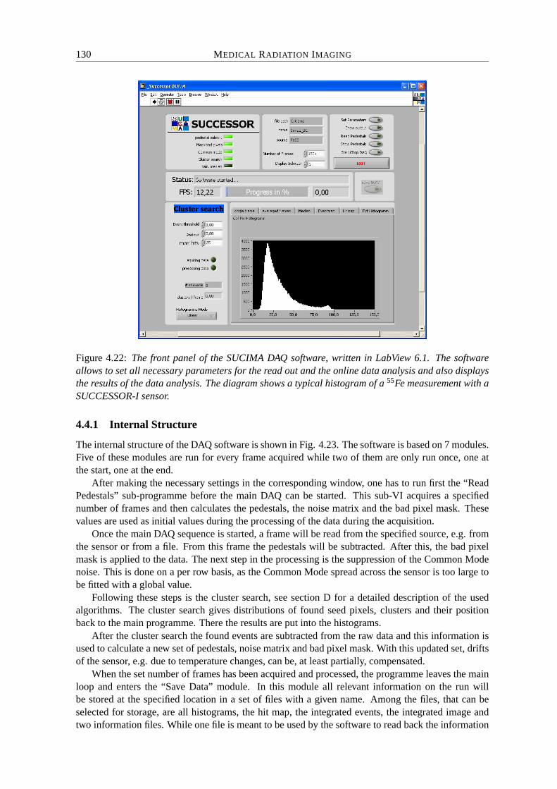
130 MEDICAL RADIATION IMAGING
Figure 4.22: The front panel of the SUCIMA DAQ software, written in LabView 6.1. The softwareallows to set all necessary parameters for the read out and the online data analysis and also displaysthe results of the data analysis. The diagram shows a typical histogram of a 55Fe measurement with aSUCCESSOR-I sensor.
4.4.1 Internal Structure
The internal structure of the DAQ software is shown in Fig. 4.23. The software is based on 7 modules.Five of these modules are run for every frame acquired while two of them are only run once, one atthe start, one at the end.
After making the necessary settings in the corresponding window, one has to run first the “ReadPedestals” sub-programme before the main DAQ can be started. This sub-VI acquires a specifiednumber of frames and then calculates the pedestals, the noise matrix and the bad pixel mask. Thesevalues are used as initial values during the processing of the data during the acquisition.
Once the main DAQ sequence is started, a frame will be read from the specified source, e.g. fromthe sensor or from a file. From this frame the pedestals will be subtracted. After this, the bad pixelmask is applied to the data. The next step in the processing is the suppression of the Common Modenoise. This is done on a per row basis, as the Common Mode spread across the sensor is too large tobe fitted with a global value.
Following these steps is the cluster search, see section D for a detailed description of the usedalgorithms. The cluster search gives distributions of found seed pixels, clusters and their positionback to the main programme. There the results are put into the histograms.
After the cluster search the found events are subtracted from the raw data and this information isused to calculate a new set of pedestals, noise matrix and bad pixel mask. With this updated set, driftsof the sensor, e.g. due to temperature changes, can be, at least partially, compensated.
When the set number of frames has been acquired and processed, the programme leaves the mainloop and enters the “Save Data” module. In this module all relevant information on the run willbe stored at the specified location in a set of files with a given name. Among the files, that can beselected for storage, are all histograms, the hit map, the integrated events, the integrated image andtwo information files. While one file is meant to be used by the software to read back the information

4.4 LABVIEW SOFTWARE FOR USB-DAQ 131
in case a re-processing is desired, the second file contains all information in a human-readable format.
Data Input
Sensor
File
Processing
PedestalSubtraction
Bad PixelMasking
Common ModeSuppression
ClusterSearch
Histogramming& Presentation
Save Data
update
Pedestals
Noise
Bad Pixel Mask
repeat n times
Initial
Pedestals
Noise
Bad Pixel Mask
Figure 4.23: This plot shows a schematic overview of the SUCIMA DAQ Software. The software issplit into 7 different modules. While the “Initial” phase is only called once at the beginning and “SaveData” only once at the end, all other modules are used for each frame acquired.
Some of the functionality of the software is sourced out into Dynamically Linked Libraries (DLL).For the USB2.0 interface this has to be done, as LabView is not able to acquire data directly from theUSB driver of the kernel. The other two DLLs used, one reads the data in the so-called “Strasbourg-format”, the other is used in the data processing, benefit from the increased performance, as the codeis compiled and is not interpreted at runtime.
To make the handling of the programme easier it uses an .INI-file to “remember” the settings fromthe last time the software was run. In this file all settings are stored.


Chapter 5
Measurements with the SUCCESSOR-ICMOS pixel sensor
In order to select the pixel geometry suited best for the SUCIMA applications from the 8 differentones on the SUCCESSOR-I CMOS pixel sensor, detailed studies were performed on these sensors. Inthis chapter the setup and the measurements on the radiation tolerance, the main focus of this thesis,and their implications on the decision for the final production will be presented.
5.1 Setup & Software
To study the performance of the various pixel geometries of the SUCCESSOR-I, it was necessary todefine a reproducible and reliable method for the sensor evaluation. After a short introduction into theirradiation setup at the IEKP and the measurement setup at LEPSI, the measurement procedure andthe analysis methods will be presented.
5.1.1 X-Ray Irradiation Setup in Karlsruhe
The X-ray setup at the IEKP was first built to study the aging of MSGCs [Erb99]. For the irradiationof the CMOS sensors some major modifications were realised, as the requirements on the irradiationare quite different.
To achieve a smaller beam spot, an adjustable collimator was mounted in front of the X-ray tube.Also a computer controlled shutter was added to allow a more precise control of the irradiation timeand thus the applied dose.
The beam profile and thus the dose applied to the sensor under study can be measured usingso-called calibration diodes. These diodes were calibrated against a known X-ray system at CERNand PIN-diodes used at CERN for dosimetry. Also an integral measurement of the dose rate wasperformed using a certified dosimeter with an ionisation chamber as sensitive device.
The temperature inside the lead container can be monitored from the PC using a PT100 tempera-ture sensor which is read out by a GPIB(1) controlled Keithley 196 DMM. The GPIB bus is also usedto communicate with the motor controller of the XY-stage. This XY-stage is used for the alignmentof the sensor for the irradiation, but also for scanning the beam spot using the calibration diode.
Later on the existing Cu-anode X-ray tube was replaced by a W-anode tube (FK60-04 fine focus)to eliminate the characteristic lines from the spectrum, which have a rather low energy, and to havethe maximum output at a shorter wavelength. The last modification of the setup was the replacementof the HV generator with a newer model (GE Inspections Debyeflex 3003) which can be computercontrolled. Both, the HV generator and the X-ray tube, are water-cooled. An overview of the systemin its final configuration is shown in Fig. 5.1.
(1)GPIB: General Purpose Interface Bus, IEEE 488
133
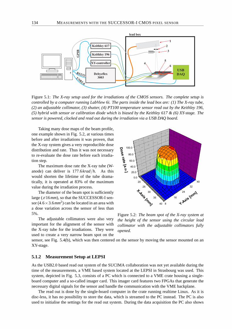
134 MEASUREMENTS WITH THE SUCCESSOR-I CMOS PIXEL SENSOR
aaaaaaaaaaaaaaaaaaaaaaaaaaaaaaaaaaaaaaaaaaaaaaaaaaaaaaaaaaaaaaaaaaaaaaaa
aaaaaaaaaaaaaaaaaaaaaaaaaaaaaaaaaaaaaa
USBDAQ
USB2.0
RS232G
PIB
Debyeflex3003
XY-controller
Keithley 196
Keithley 617
1
2
3
45
6
lead box
Figure 5.1: The X-ray setup used for the irradiations of the CMOS sensors. The complete setup iscontrolled by a computer running LabView 6i. The parts inside the lead box are: (1) The X-ray tube,(2) an adjustable collimator, (3) shutter, (4) PT100 temperature sensor read out by the Keithley 196,(5) hybrid with sensor or calibration diode which is biased by the Keithley 617 & (6) XY-stage. Thesensor is powered, clocked and read out during the irradiation via a USB DAQ board.
Figure 5.2: The beam spot of the X-ray system atthe height of the sensor using the circular leadcollimator with the adjustable collimators fullyopened.
Taking many dose maps of the beam profile,one example shown in Fig. 5.2, at various timesbefore and after irradiations it was proven, thatthe X-ray system gives a very reproducible dosedistribution and rate. Thus it was not necessaryto re-evaluate the dose rate before each irradia-tion step.
The maximum dose rate the X-ray tube (W-anode) can deliver is 177.6krad/h. As thiswould shorten the lifetime of the tube drama-tically, it is operated at 83% of the maximumvalue during the irradiation process.
The diameter of the beam spot is sufficientlylarge (16mm), so that the SUCCESSOR-I sen-sor (4.6×3.6mm2) can be located in an area witha dose variation across the sensor of less than5%.
The adjustable collimators were also veryimportant for the alignment of the sensor withthe X-ray tube for the irradiations. They wereused to create a very narrow beam spot on thesensor, see Fig. 5.4(b), which was then centered on the sensor by moving the sensor mounted on anXY-stage.
5.1.2 Measurement Setup at LEPSI
As the USB2.0 based read out system of the SUCIMA collaboration was not yet available during thetime of the measurements, a VME based system located at the LEPSI in Strasbourg was used. Thissystem, depicted in Fig. 5.3, consists of a PC which is connected to a VME crate housing a single-board computer and a so-called imager card. This imager card features two FPGAs that generate thenecessary digital signals for the sensor and handle the communication with the VME backplane.
The read out is done by the single-board computer in the crate running realtime Linux. As it isdisc-less, it has no possibility to store the data, which is streamed to the PC instead. The PC is alsoused to initialise the settings for the read out system. During the data acquisition the PC also shows

5.1 SETUP & SOFTWARE 135
an online display of the raw data, allowing some quality control of the data. For a more detaileddescription of the setup refer to [Dev03].
aaaaaaaaaaaaaaaaaaaaaaaaaaaaaaaaaaaaaaaaaaaaaaaaaaaaaaaaaaaaaaaaaaaaaaaa
aaaaaaaaaaaaaaaaaaaaaaaaaaaaaaaaaaaaaa
aaaaaaaaaaaaaaaaaaaaaaaaaaaaaaaaaaaaaaaaaaaaaaaaaaaaaaaaaaaaaaaaaaaaaaaaaaaaaaaaaaaaaaaaaaaaaaaaaaaaaaaaaaaaaaaaaaaaaaaaaaaaaaaaaaaaaaaaaaaaaaaaaaaaaaaaaaaaaaaaaaaaaaaaaaaaaaaaaaaaaaaaaaaaaaaaaaaaaaaaaaaaaaaaaaaaaaaaaaaaaaaaaaaaaaaaaaaaaaaaaaaaaaaaaaaaaaaaaaaaaaaaaaaaaaaaaaaaaaaaaaaaaaaaaaaaaaaaaaaaaaaaaaaaaaaaaaaaaaaaaaaaaaaaaa
°C
aaaaaaaaaaaaaaaaaaaaaaaaaaaaaaaaaaaaaaaaaaaaaaaaaaaaaaaaaaaaaaaaaaaaaaaaaaaaaaaaaaaaaaaaaaaaaaaaaaaaaaaaaaaaaaaaaaaaaaaaaaaaaaaaaaaaaaaaaaaaaaaaaaaaaaaaaaaaaaaaaaaaaaaaaaaaaaaaaaaaaaaaaaaaaaaaaaaaaaaaaaaaaaaaaaaaaaaaaaaaaaaaaaaaaaaaaaaaaaaaaaaaaaaaaaaaaaaaaaaaaaaaaaaaaaaaaaaaaaaaaaaaaaaaaaaaaaaaaaaaaaaaaaaaaaaaaaaaaaaa
sin
gle
bo
ard
com
pu
ter
Ima
ger
Ca
rd
repeater
TCP/IP
Figure 5.3: The setup at the LEPSI, as it was used for the measurements on the CMOS sensors. Sensoris located in a temperature controlled box and connected to a repeater board. Through this board it issupplied with power and all digital signals. Also the analogue signals coming from the sensors passthrough the repeater and are amplified there. The VME crate, housing the so-called imager card, iscontrolled by a single-board computer. The data is streamed to a Linux PC, which is also used to setthe parameters for the DAQ.
5.1.3 Measurement & Irradiation Procedure
To ensure the reproducibility of the acquired data procedures for the measurement and the irradiationwere defined and applied to all measured sensors. Also the most important parameters set for themeasurements were recorded. The procedures are described in the following:
• Measurements: There are two different types of measurements: the leakage current measure-ment and the recording of 55Fe -spectra. Both sets of measurements are done for each of thepixel matrices.
– Leakage Current: As the leakage currents are very small for some pixel geometries, espe-cially before the irradiation, more frames than in the standard mode are read out betweenresets to achieve a longer integration time and thus higher integrated values. These valuesare then divided by the number of frames read to re-normalise them.
When measuring highly irradiated devices, it was noticed, that the method mentionedabove ran into saturation and was not applicable any more. Additionally, the gain ofthe repeater was enhanced by a factor three in comparison to measurements with otherprototype chips.
To calculate the leakage current, 10000 frames are acquired without a source above thesensor. From these frames the pedestals are calculated. The distribution of the pedestalsof the sensor is fit with a Gaussian distribution.
This method is precise enough at low doses and is still usable at high doses. The resultsfor low doses are in very good agreement with those taken with the first method.
The leakage current measurements are done at the temperatures −15 C, 0 C, 10 C and20 C.
– 55Fe Spectra: Two things can be learned from the 55Fe spectra. The first is the position ofthe peak generated by the 5.89keV gammas converted in the small depletion layer directlybeneath the collection diode, see Fig. 3.9. As mentioned above, from the position of thepeak the device can be calibrated.
The second important characteristic is the charge collection efficiency (CCE). By com-paring the spectra of the seed pixels and the clusters one can learn, wether the CCE haschanged due to the irradiation of the device.
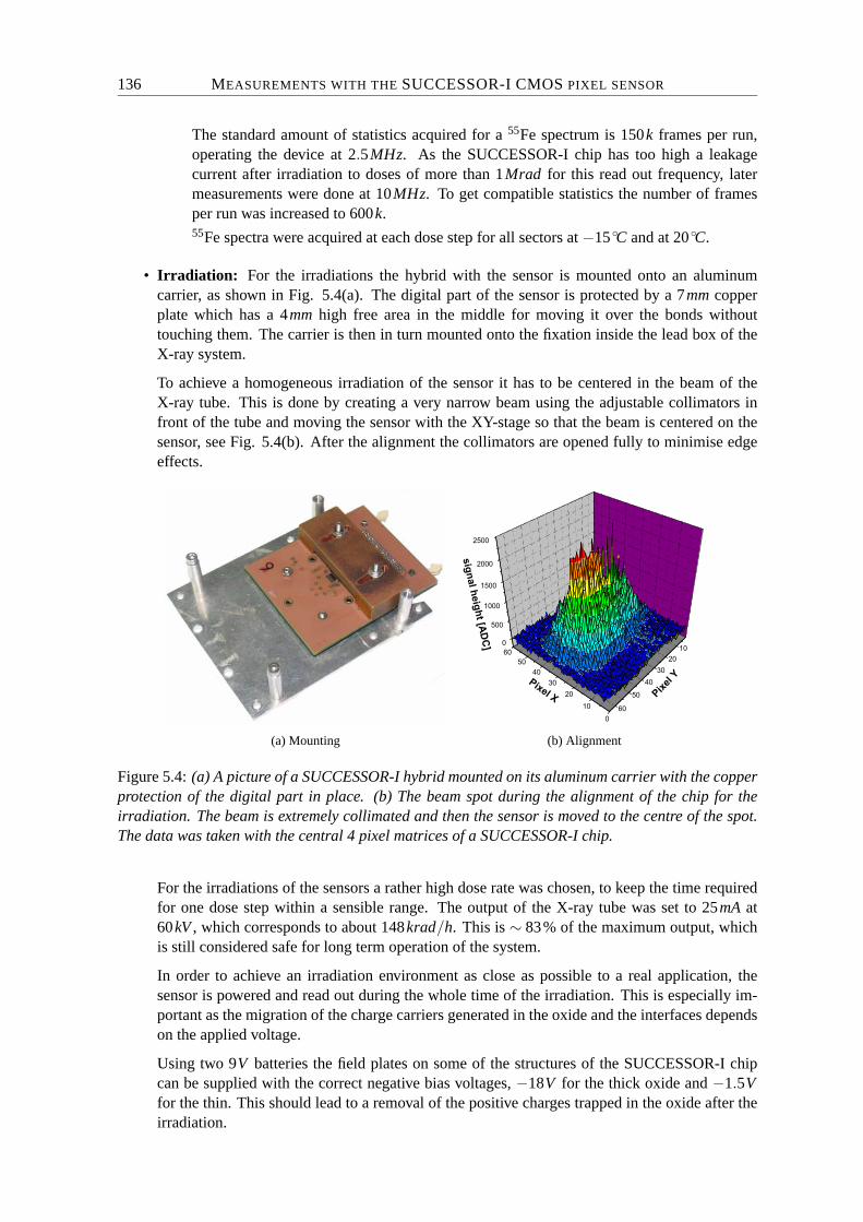
136 MEASUREMENTS WITH THE SUCCESSOR-I CMOS PIXEL SENSOR
The standard amount of statistics acquired for a 55Fe spectrum is 150k frames per run,operating the device at 2.5MHz. As the SUCCESSOR-I chip has too high a leakagecurrent after irradiation to doses of more than 1Mrad for this read out frequency, latermeasurements were done at 10MHz. To get compatible statistics the number of framesper run was increased to 600k.55Fe spectra were acquired at each dose step for all sectors at −15 C and at 20 C.
• Irradiation: For the irradiations the hybrid with the sensor is mounted onto an aluminumcarrier, as shown in Fig. 5.4(a). The digital part of the sensor is protected by a 7mm copperplate which has a 4mm high free area in the middle for moving it over the bonds withouttouching them. The carrier is then in turn mounted onto the fixation inside the lead box of theX-ray system.
To achieve a homogeneous irradiation of the sensor it has to be centered in the beam of theX-ray tube. This is done by creating a very narrow beam using the adjustable collimators infront of the tube and moving the sensor with the XY-stage so that the beam is centered on thesensor, see Fig. 5.4(b). After the alignment the collimators are opened fully to minimise edgeeffects.
(a) Mounting (b) Alignment
Figure 5.4: (a) A picture of a SUCCESSOR-I hybrid mounted on its aluminum carrier with the copperprotection of the digital part in place. (b) The beam spot during the alignment of the chip for theirradiation. The beam is extremely collimated and then the sensor is moved to the centre of the spot.The data was taken with the central 4 pixel matrices of a SUCCESSOR-I chip.
For the irradiations of the sensors a rather high dose rate was chosen, to keep the time requiredfor one dose step within a sensible range. The output of the X-ray tube was set to 25mA at60kV , which corresponds to about 148krad/h. This is ∼ 83% of the maximum output, whichis still considered safe for long term operation of the system.
In order to achieve an irradiation environment as close as possible to a real application, thesensor is powered and read out during the whole time of the irradiation. This is especially im-portant as the migration of the charge carriers generated in the oxide and the interfaces dependson the applied voltage.
Using two 9V batteries the field plates on some of the structures of the SUCCESSOR-I chipcan be supplied with the correct negative bias voltages, −18V for the thick oxide and −1.5Vfor the thin. This should lead to a removal of the positive charges trapped in the oxide after theirradiation.
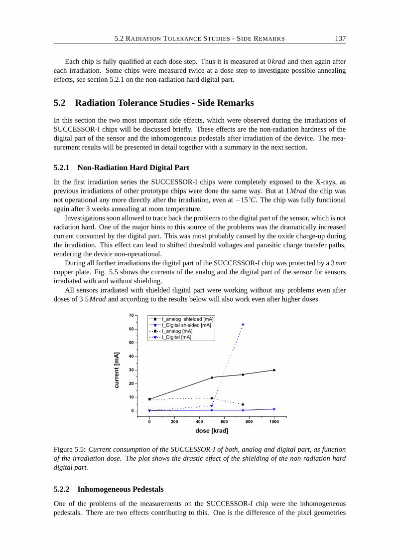
5.2 RADIATION TOLERANCE STUDIES - SIDE REMARKS 137
Each chip is fully qualified at each dose step. Thus it is measured at 0krad and then again aftereach irradiation. Some chips were measured twice at a dose step to investigate possible annealingeffects, see section 5.2.1 on the non-radiation hard digital part.
5.2 Radiation Tolerance Studies - Side Remarks
In this section the two most important side effects, which were observed during the irradiations ofSUCCESSOR-I chips will be discussed briefly. These effects are the non-radiation hardness of thedigital part of the sensor and the inhomogeneous pedestals after irradiation of the device. The mea-surement results will be presented in detail together with a summary in the next section.
5.2.1 Non-Radiation Hard Digital Part
In the first irradiation series the SUCCESSOR-I chips were completely exposed to the X-rays, asprevious irradiations of other prototype chips were done the same way. But at 1Mrad the chip wasnot operational any more directly after the irradiation, even at −15 C. The chip was fully functionalagain after 3 weeks annealing at room temperature.
Investigations soon allowed to trace back the problems to the digital part of the sensor, which is notradiation hard. One of the major hints to this source of the problems was the dramatically increasedcurrent consumed by the digital part. This was most probably caused by the oxide charge-up duringthe irradiation. This effect can lead to shifted threshold voltages and parasitic charge transfer paths,rendering the device non-operational.
During all further irradiations the digital part of the SUCCESSOR-I chip was protected by a 3mmcopper plate. Fig. 5.5 shows the currents of the analog and the digital part of the sensor for sensorsirradiated with and without shielding.
All sensors irradiated with shielded digital part were working without any problems even afterdoses of 3.5Mrad and according to the results below will also work even after higher doses.
Figure 5.5: Current consumption of the SUCCESSOR-I of both, analog and digital part, as functionof the irradiation dose. The plot shows the drastic effect of the shielding of the non-radiation harddigital part.
5.2.2 Inhomogeneous Pedestals
One of the problems of the measurements on the SUCCESSOR-I chip were the inhomogeneouspedestals. There are two effects contributing to this. One is the difference of the pixel geometries
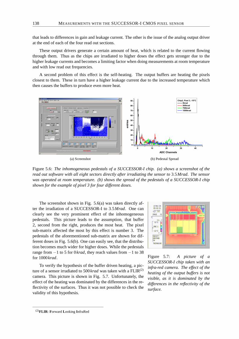
138 MEASUREMENTS WITH THE SUCCESSOR-I CMOS PIXEL SENSOR
that leads to differences in gain and leakage current. The other is the issue of the analog output driverat the end of each of the four read out sections.
These output drivers generate a certain amount of heat, which is related to the current flowingthrough them. Thus as the chips are irradiated to higher doses the effect gets stronger due to thehigher leakage currents and becomes a limiting factor when doing measurements at room temperatureand with low read out frequencies.
A second problem of this effect is the self-heating. The output buffers are heating the pixelsclosest to them. These in turn have a higher leakage current due to the increased temperature whichthen causes the buffers to produce even more heat.
(a) Screenshot (b) Pedestal Spread
Figure 5.6: The inhomogeneous pedestals of a SUCCESSOR-I chip. (a) shows a screenshot of theread out software with all eight sectors directly after irradiating the sensor to 3.5Mrad. The sensorwas operated at room temperature. (b) shows the spread of the pedestals of a SUCCESSOR-I chipshown for the example of pixel 3 for four different doses.
Figure 5.7: A picture of aSUCCESSOR-I chip taken with aninfra-red camera. The effect of theheating of the output buffers is notvisible, as it is dominated by thedifferences in the reflectivity of thesurface.
The screenshot shown in Fig. 5.6(a) was taken directly af-ter the irradiation of a SUCCESSOR-I to 3.5Mrad. One canclearly see the very prominent effect of the inhomogeneouspedestals. This picture leads to the assumption, that buffer2, second from the right, produces the most heat. The pixelsub-matrix affected the most by this effect is number 3. Thepedestals of the aforementioned sub-matrix are shown for dif-ferent doses in Fig. 5.6(b). One can easily see, that the distribu-tion becomes much wider for higher doses. While the pedestalsrange from −1 to 5 for 0krad, they reach values from −1 to 38for 1000krad.
To verify the hypothesis of the buffer driven heating, a pic-ture of a sensor irradiated to 500krad was taken with a FLIR(2)
camera. This picture is shown in Fig. 5.7. Unfortunately, theeffect of the heating was dominated by the differences in the re-flectivity of the surfaces. Thus it was not possible to check thevalidity of this hypothesis.
(2)FLIR: Forward Looking InfraRed
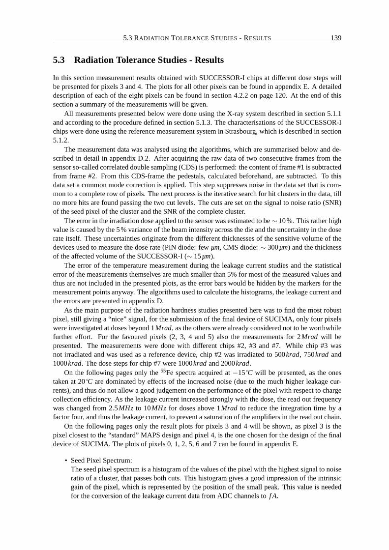
5.3 RADIATION TOLERANCE STUDIES - RESULTS 139
5.3 Radiation Tolerance Studies - Results
In this section measurement results obtained with SUCCESSOR-I chips at different dose steps willbe presented for pixels 3 and 4. The plots for all other pixels can be found in appendix E. A detaileddescription of each of the eight pixels can be found in section 4.2.2 on page 120. At the end of thissection a summary of the measurements will be given.
All measurements presented below were done using the X-ray system described in section 5.1.1and according to the procedure defined in section 5.1.3. The characterisations of the SUCCESSOR-Ichips were done using the reference measurement system in Strasbourg, which is described in section5.1.2.
The measurement data was analysed using the algorithms, which are summarised below and de-scribed in detail in appendix D.2. After acquiring the raw data of two consecutive frames from thesensor so-called correlated double sampling (CDS) is performed: the content of frame #1 is subtractedfrom frame #2. From this CDS-frame the pedestals, calculated beforehand, are subtracted. To thisdata set a common mode correction is applied. This step suppresses noise in the data set that is com-mon to a complete row of pixels. The next process is the iterative search for hit clusters in the data, tillno more hits are found passing the two cut levels. The cuts are set on the signal to noise ratio (SNR)of the seed pixel of the cluster and the SNR of the complete cluster.
The error in the irradiation dose applied to the sensor was estimated to be ∼ 10%. This rather highvalue is caused by the 5% variance of the beam intensity across the die and the uncertainty in the doserate itself. These uncertainties originate from the different thicknesses of the sensitive volume of thedevices used to measure the dose rate (PIN diode: few µm, CMS diode: ∼ 300µm) and the thicknessof the affected volume of the SUCCESSOR-I (∼ 15µm).
The error of the temperature measurement during the leakage current studies and the statisticalerror of the measurements themselves are much smaller than 5% for most of the measured values andthus are not included in the presented plots, as the error bars would be hidden by the markers for themeasurement points anyway. The algorithms used to calculate the histograms, the leakage current andthe errors are presented in appendix D.
As the main purpose of the radiation hardness studies presented here was to find the most robustpixel, still giving a “nice” signal, for the submission of the final device of SUCIMA, only four pixelswere investigated at doses beyond 1Mrad, as the others were already considered not to be worthwhilefurther effort. For the favoured pixels (2, 3, 4 and 5) also the measurements for 2Mrad will bepresented. The measurements were done with different chips #2, #3 and #7. While chip #3 wasnot irradiated and was used as a reference device, chip #2 was irradiated to 500krad, 750krad and1000krad. The dose steps for chip #7 were 1000krad and 2000krad.
On the following pages only the 55Fe spectra acquired at −15 C will be presented, as the onestaken at 20 C are dominated by effects of the increased noise (due to the much higher leakage cur-rents), and thus do not allow a good judgement on the performance of the pixel with respect to chargecollection efficiency. As the leakage current increased strongly with the dose, the read out frequencywas changed from 2.5MHz to 10MHz for doses above 1Mrad to reduce the integration time by afactor four, and thus the leakage current, to prevent a saturation of the amplifiers in the read out chain.
On the following pages only the result plots for pixels 3 and 4 will be shown, as pixel 3 is thepixel closest to the “standard” MAPS design and pixel 4, is the one chosen for the design of the finaldevice of SUCIMA. The plots of pixels 0, 1, 2, 5, 6 and 7 can be found in appendix E.
• Seed Pixel Spectrum:The seed pixel spectrum is a histogram of the values of the pixel with the highest signal to noiseratio of a cluster, that passes both cuts. This histogram gives a good impression of the intrinsicgain of the pixel, which is represented by the position of the small peak. This value is neededfor the conversion of the leakage current data from ADC channels to f A.

140 MEASUREMENTS WITH THE SUCCESSOR-I CMOS PIXEL SENSOR
• Cluster Spectrum:In the cluster spectrum the sum of the nine pixels with the highest signal to noise ratio inthe cluster is histogrammed. From the cluster spectra one can learn about the charge sharingbetween the pixels. Only the plots for a cluster size of nine pixels are shown. For this clustersize ∼ 95% of the deposited charge is collected. Due to the used algorithm, larger cluster (> 15)sizes are affected by the noise of the matrix, which will lead to a decreased value of the sum.
• Noise Spectrum:The development of the noise spectrum as a function of the irradiation dose gives a good indi-cation on the usefulness of a pixel for dosimetry applications, where a high signal to noise ratiois required to reach the necessary precision.
• Leakage Current:The leakage current of a pixel is also an important factor, as it imposes limits for the maximumintegration time and temperature at which the device should be operated. Outside these limitsthe leakage current will drain the collecting diode and limit the dynamic range of the detectorand it can saturate the output amplifiers.
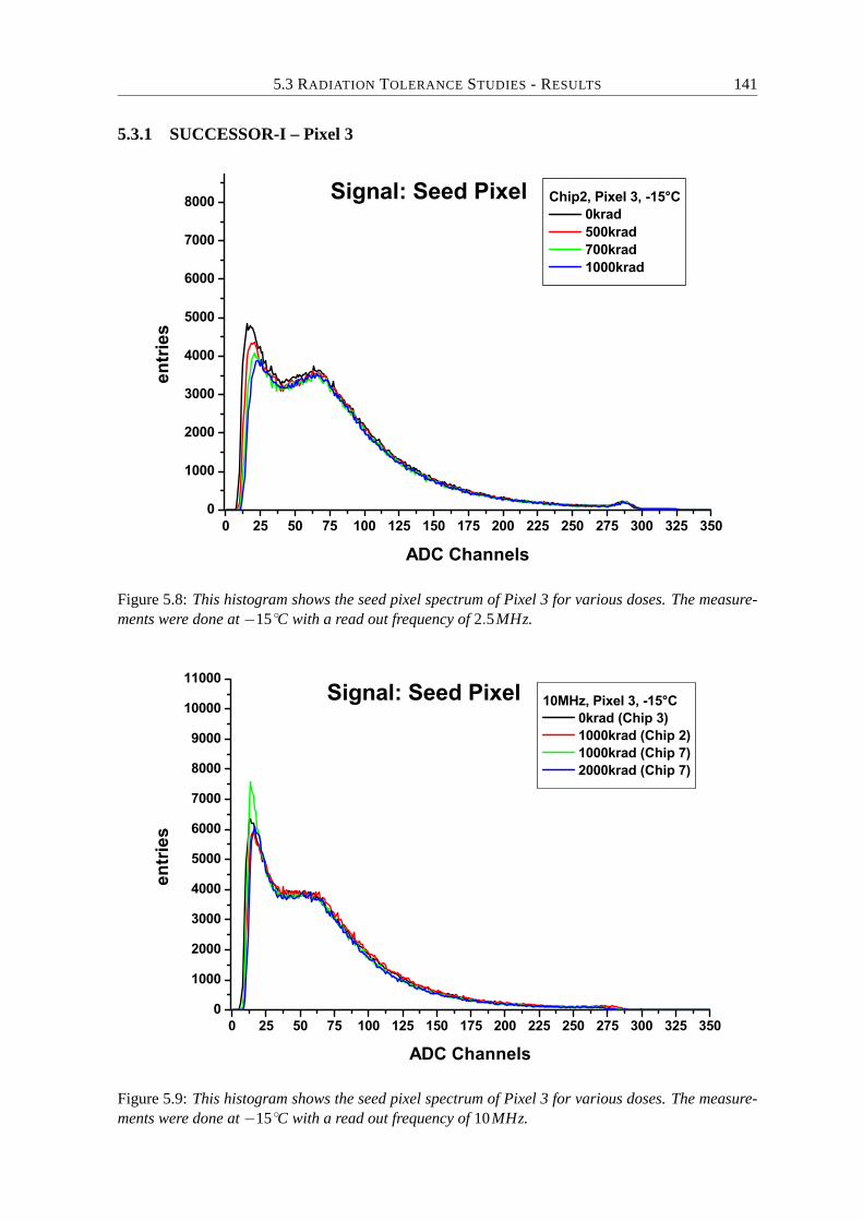
5.3 RADIATION TOLERANCE STUDIES - RESULTS 141
5.3.1 SUCCESSOR-I – Pixel 3
Figure 5.8: This histogram shows the seed pixel spectrum of Pixel 3 for various doses. The measure-ments were done at −15 C with a read out frequency of 2.5MHz.
Figure 5.9: This histogram shows the seed pixel spectrum of Pixel 3 for various doses. The measure-ments were done at −15 C with a read out frequency of 10MHz.
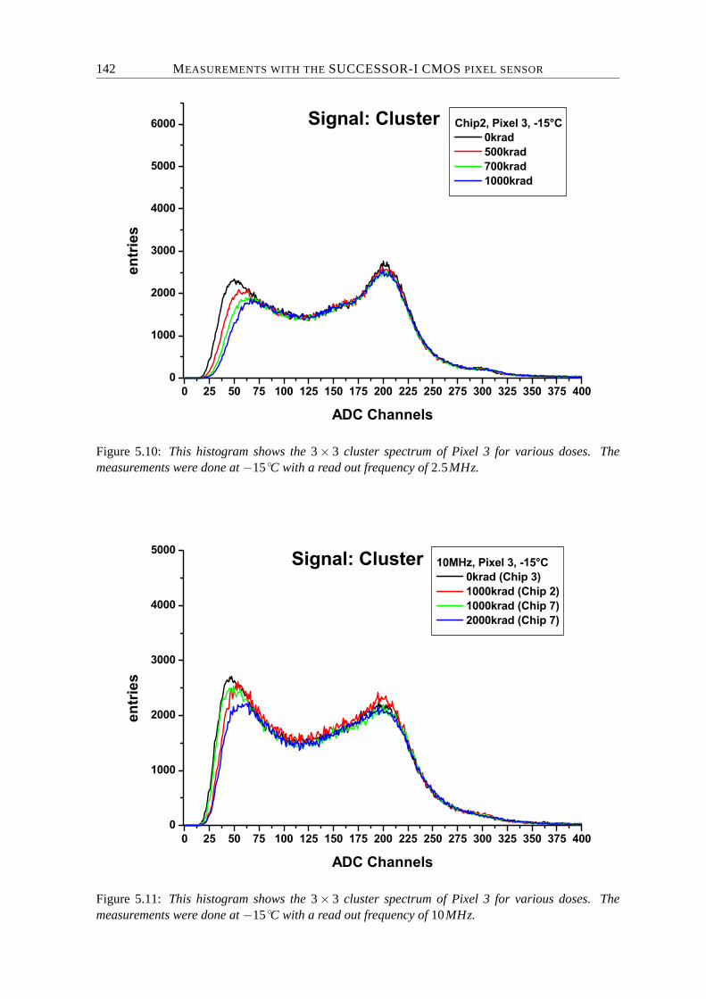
142 MEASUREMENTS WITH THE SUCCESSOR-I CMOS PIXEL SENSOR
Figure 5.10: This histogram shows the 3 × 3 cluster spectrum of Pixel 3 for various doses. Themeasurements were done at −15 C with a read out frequency of 2.5MHz.
Figure 5.11: This histogram shows the 3 × 3 cluster spectrum of Pixel 3 for various doses. Themeasurements were done at −15 C with a read out frequency of 10MHz.
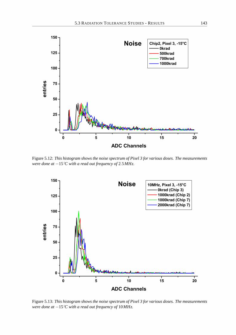
5.3 RADIATION TOLERANCE STUDIES - RESULTS 143
Figure 5.12: This histogram shows the noise spectrum of Pixel 3 for various doses. The measurementswere done at −15 C with a read out frequency of 2.5MHz.
Figure 5.13: This histogram shows the noise spectrum of Pixel 3 for various doses. The measurementswere done at −15 C with a read out frequency of 10MHz.
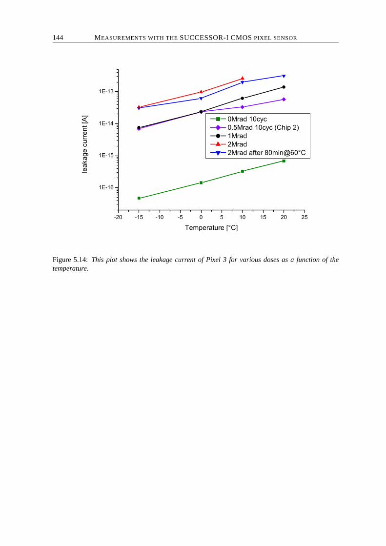
144 MEASUREMENTS WITH THE SUCCESSOR-I CMOS PIXEL SENSOR
Figure 5.14: This plot shows the leakage current of Pixel 3 for various doses as a function of thetemperature.
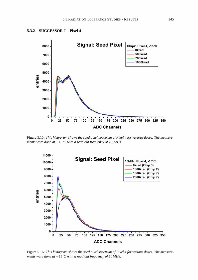
5.3 RADIATION TOLERANCE STUDIES - RESULTS 145
5.3.2 SUCCESSOR-I – Pixel 4
Figure 5.15: This histogram shows the seed pixel spectrum of Pixel 4 for various doses. The measure-ments were done at −15 C with a read out frequency of 2.5MHz.
Figure 5.16: This histogram shows the seed pixel spectrum of Pixel 4 for various doses. The measure-ments were done at −15 C with a read out frequency of 10MHz.
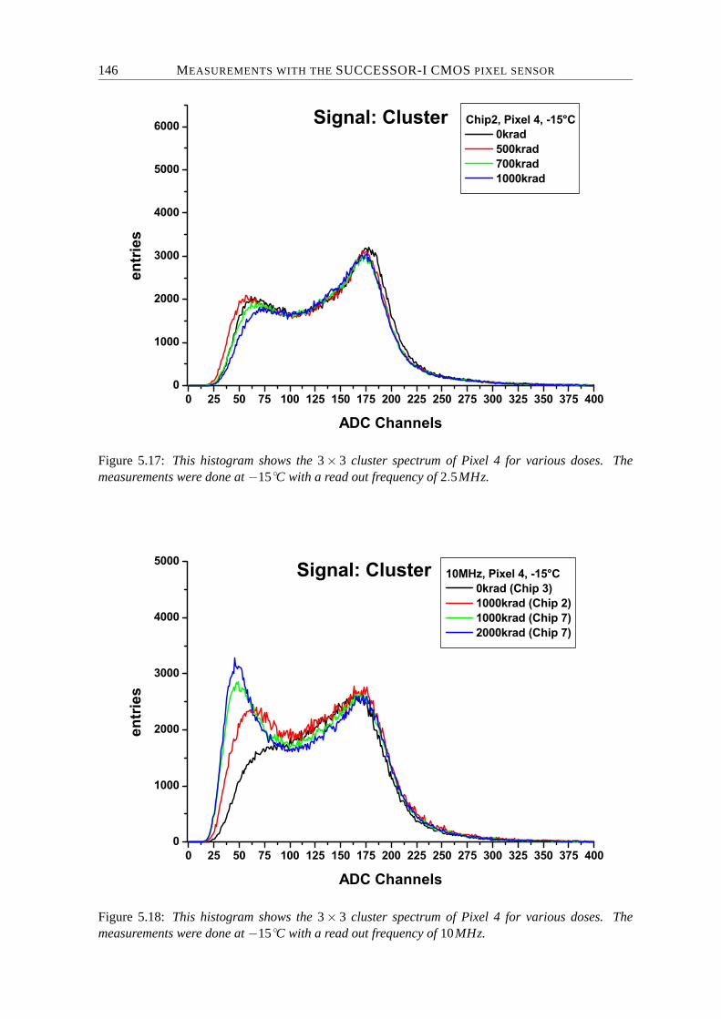
146 MEASUREMENTS WITH THE SUCCESSOR-I CMOS PIXEL SENSOR
Figure 5.17: This histogram shows the 3 × 3 cluster spectrum of Pixel 4 for various doses. Themeasurements were done at −15 C with a read out frequency of 2.5MHz.
Figure 5.18: This histogram shows the 3 × 3 cluster spectrum of Pixel 4 for various doses. Themeasurements were done at −15 C with a read out frequency of 10MHz.
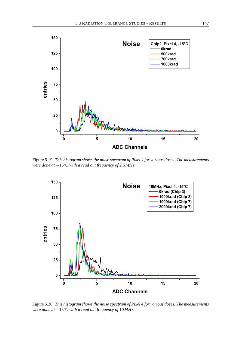
5.3 RADIATION TOLERANCE STUDIES - RESULTS 147
Figure 5.19: This histogram shows the noise spectrum of Pixel 4 for various doses. The measurementswere done at −15 C with a read out frequency of 2.5MHz.
Figure 5.20: This histogram shows the noise spectrum of Pixel 4 for various doses. The measurementswere done at −15 C with a read out frequency of 10MHz.
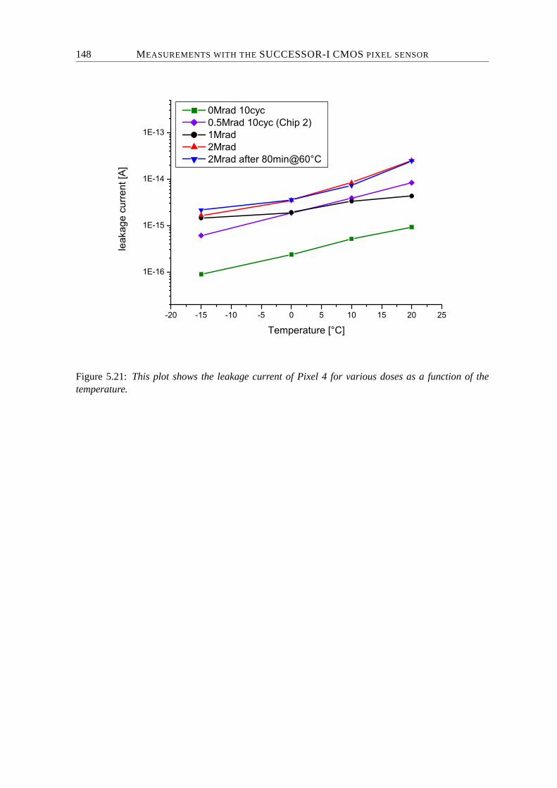
148 MEASUREMENTS WITH THE SUCCESSOR-I CMOS PIXEL SENSOR
Figure 5.21: This plot shows the leakage current of Pixel 4 for various doses as a function of thetemperature.

5.3 RADIATION TOLERANCE STUDIES - RESULTS 149
5.3.3 Summary
In this summary, a short comparison of the cluster and noise spectra for the four favoured pixels willbe followed by a review of the results from the leakage current measurements. At the end of thissection the most important criteria will be summarised in two tables. As a conclusion the choice ofthe pixel used in the next generation of CMOS detectors will be motivated, based on the measurementspresented here.
In previous measurements on CMOS detectors, it was observed, that a substantial charge lossaffected the performance of the device already at relatively low doses of 100krad [Dep02]. Thiseffect is observable as a shift of the peak in the cluster spectrum towards lower values. The shift of thecluster peak is also observable for some of the pixels of SUCCESSOR-I at T = −15 C, but only forlonger integration times and even then only to a non-significant extent (< 2%). At higher temperatures(T = 20 C), the effect becomes more prominent, but is still much smaller than previously observed.
Another effect that was established in previous studies was the decreased gain of the amplificationinside the detector [Dep02]. The effect reveals itself as a shift of the small 55Fe peaks in the seedpixel spectrum towards lower values. Again, this effect was not observed with the SUCCESSOR-Idetector. Even after 2Mrad, the position of the small peak remains stable, within the precision of themeasurement.
In the current understanding, this stability of the intrinsic gain has to be accredited to the newerCMOS processes which use a much thinner gate oxide and thus are less receptive to damage effects inthe oxide, as mentioned in section 3.4.2. This also contributes to the stability of the charge collectionprocess. An additional beneficial effect for the charge collection is the swapping of the source and thedrain of the reset transistor, which removes a possible parasitic charge transfer path, see section 3.4.2.
(a) −15C, 10MHz (b) 20C, 2.5MHz
Figure 5.22: The noise spectra of pixel 5. (a) shows the noise distribution of this pixel for T =−15 Cand a read out frequency of 10MHz. In (b) the noise distribution is depicted for T = 20 C and2.5MHz. While the noise is not affected by the irradiation in plot (a), it is clearly increasing with thedose in plot (b), which is mostly caused by the increased leakage current.
At T = −15 C the noise of the detector, also a very crucial parameter for the evaluation, is alsoalmost not affected by the irradiation of the detector, even up to 2Mrad. This can be seen in the noisehistograms of the individual pixels, one example is shown in Fig. 5.22(a) for pixel 5 (10MHz). AtT = 20 C the noise is 2 to 3 times higher and increases with the dose, which is mostly related to theincreased leakage current, see Fig. 5.22(b) which shows the noise distribution of pixel 5 for a read outfrequency of 2.5MHz and doses up to 1Mrad.
One of the most important parameters of a detector is the signal to noise ratio (SNR). In this thesisthe SNR is defined as the position of the peak in the cluster spectrum divided by the most probablevalue of the corresponding noise distribution. In Fig. 5.23(a) the cluster spectra of the pixels 2, 3, 4 and
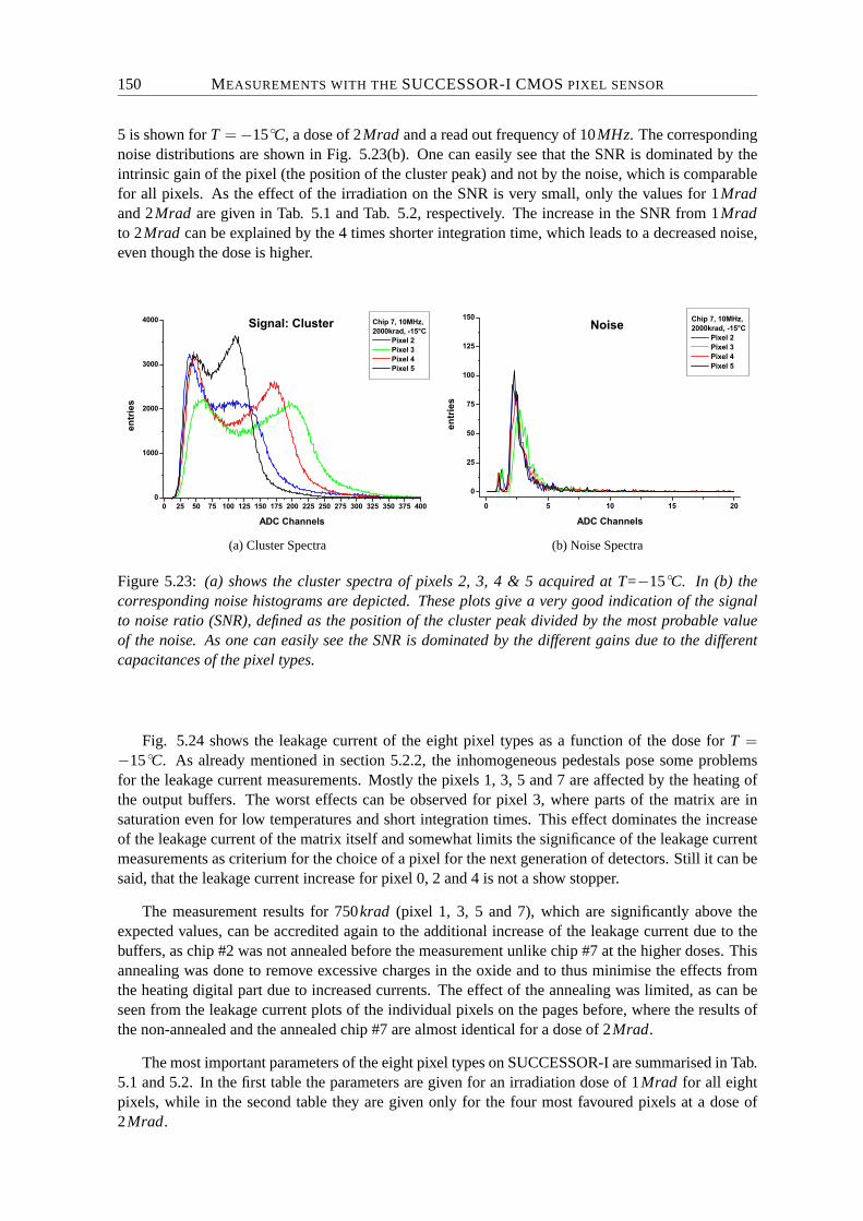
150 MEASUREMENTS WITH THE SUCCESSOR-I CMOS PIXEL SENSOR
5 is shown for T = −15 C, a dose of 2Mrad and a read out frequency of 10MHz. The correspondingnoise distributions are shown in Fig. 5.23(b). One can easily see that the SNR is dominated by theintrinsic gain of the pixel (the position of the cluster peak) and not by the noise, which is comparablefor all pixels. As the effect of the irradiation on the SNR is very small, only the values for 1Mradand 2Mrad are given in Tab. 5.1 and Tab. 5.2, respectively. The increase in the SNR from 1Mradto 2Mrad can be explained by the 4 times shorter integration time, which leads to a decreased noise,even though the dose is higher.
(a) Cluster Spectra (b) Noise Spectra
Figure 5.23: (a) shows the cluster spectra of pixels 2, 3, 4 & 5 acquired at T=−15 C. In (b) thecorresponding noise histograms are depicted. These plots give a very good indication of the signalto noise ratio (SNR), defined as the position of the cluster peak divided by the most probable valueof the noise. As one can easily see the SNR is dominated by the different gains due to the differentcapacitances of the pixel types.
Fig. 5.24 shows the leakage current of the eight pixel types as a function of the dose for T =−15 C. As already mentioned in section 5.2.2, the inhomogeneous pedestals pose some problemsfor the leakage current measurements. Mostly the pixels 1, 3, 5 and 7 are affected by the heating ofthe output buffers. The worst effects can be observed for pixel 3, where parts of the matrix are insaturation even for low temperatures and short integration times. This effect dominates the increaseof the leakage current of the matrix itself and somewhat limits the significance of the leakage currentmeasurements as criterium for the choice of a pixel for the next generation of detectors. Still it can besaid, that the leakage current increase for pixel 0, 2 and 4 is not a show stopper.
The measurement results for 750krad (pixel 1, 3, 5 and 7), which are significantly above theexpected values, can be accredited again to the additional increase of the leakage current due to thebuffers, as chip #2 was not annealed before the measurement unlike chip #7 at the higher doses. Thisannealing was done to remove excessive charges in the oxide and to thus minimise the effects fromthe heating digital part due to increased currents. The effect of the annealing was limited, as can beseen from the leakage current plots of the individual pixels on the pages before, where the results ofthe non-annealed and the annealed chip #7 are almost identical for a dose of 2Mrad.
The most important parameters of the eight pixel types on SUCCESSOR-I are summarised in Tab.5.1 and 5.2. In the first table the parameters are given for an irradiation dose of 1Mrad for all eightpixels, while in the second table they are given only for the four most favoured pixels at a dose of2Mrad.
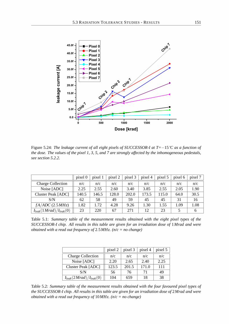
5.3 RADIATION TOLERANCE STUDIES - RESULTS 151
Figure 5.24: The leakage current of all eight pixels of SUCCESSOR-I at T=−15 C as a function ofthe dose. The values of the pixel 1, 3, 5, and 7 are strongly affected by the inhomogeneous pedestals,see section 5.2.2.
pixel 0 pixel 1 pixel 2 pixel 3 pixel 4 pixel 5 pixel 6 pixel 7
Charge Collection n/c n/c n/c n/c n/c n/c n/c n/cNoise [ADC] 2.25 2.55 2.60 3.40 3.85 2.55 2.05 1.90
Cluster Peak [ADC] 140.5 146.5 128.0 202.0 173.5 115.0 64.0 30.5S/N 62 58 49 59 45 45 31 16
f A/ADC (2.5MHz) 1.82 1.72 4.28 9.26 1.30 1.55 1.09 1.08Ileak(1Mrad)/Ileak(0) 23 220 67 271 12 23 5 6
Table 5.1: Summary table of the measurement results obtained with the eight pixel types of theSUCCESSOR-I chip. All results in this table are given for an irradiation dose of 1Mrad and wereobtained with a read out frequency of 2.5MHz. (n/c = no change)
pixel 2 pixel 3 pixel 4 pixel 5
Charge Collection n/c n/c n/c n/cNoise [ADC] 2.20 2.65 2.40 2.25
Cluster Peak [ADC] 123.5 201.5 171.0 111S/N 56 76 71 49
Ileak(2Mrad)/Ileak(0) 104 659 18 38
Table 5.2: Summary table of the measurement results obtained with the four favoured pixel types ofthe SUCCESSOR-I chip. All results in this table are given for an irradiation dose of 2Mrad and wereobtained with a read out frequency of 10MHz. (n/c = no change)

152 MEASUREMENTS WITH THE SUCCESSOR-I CMOS PIXEL SENSOR
Choosing a pixel geometry
The decision on the pixel type to be used in the next generation of CMOS pixel detectors for theSUCIMA project was taken based on the measurement results presented above. Which pixel did wechoose and based on which criteria?
As can be easily seen from the presented results, the old worries of charge loss and gain variationdue to irradiation of the detector did not affect any of the eight tested pixel types. Also the signal tonoise ratio is well above any critical value for the pixels 1 to 5. Pixels 6 and 7 were only regarded astest structures and never really as a possible candidate for the next detector iteration.
So finally the decisive parameters were the gain and the leakage current. The gain should beneither too low (poor detection efficiency) nor too high (possible risk of saturation in high dose rateenvironments). But the most important issue was the leakage current, which effectively limits theoperational range of the device with respect to temperature and integration time. The pixel typematching these criteria best, was pixel 4. Consequently, the design of the pixels in the SUCCESSOR-V detector is based on the geometry of pixel 4 of the SUCCESSOR-I.
This new detector, SUCCESSOR-V, will allow to make more than 10000 measurements of abrachytherapy source under worst case conditions (measurement time: 10s, dose rate: 20rad/s).Older pixel designs would have allow only a few hundred measurements as their performance de-graded very fast with increasing dose.
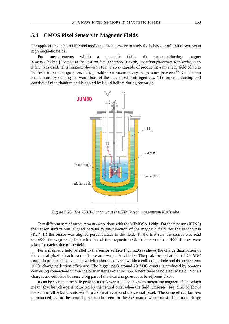
5.4 CMOS PIXEL SENSORS IN MAGNETIC FIELDS 153
5.4 CMOS Pixel Sensors in Magnetic Fields
For applications in both HEP and medicine it is necessary to study the behaviour of CMOS sensors inhigh magnetic fields.
For measurements within a magnetic field, the superconducting magnetJUMBO [Sch99] located at the Institut fur Technische Physik, Forschungszentrum Karlsruhe, Ger-many, was used. This magnet, shown in Fig. 5.25 is capable of producing a magnetic field of up to10 Tesla in our configuration. It is possible to measure at any temperature between 77K and roomtemperature by cooling the warm bore of the magnet with nitrogen gas. The superconducting coilconsists of niob titanium and is cooled by liquid helium during operation.
NbTi coils
NbSn coils
detector
Figure 5.25: The JUMBO magnet at the ITP, Forschungszentrum Karlsruhe
Two different sets of measurements were done with the MIMOSA-I chip. For the first run (RUN I)the sensor surface was aligned parallel to the direction of the magnetic field, for the second run(RUN II) the sensor was aligned perpendicular to the field. In the first run, the sensor was readout 6000 times (frames) for each value of the magnetic field, in the second run 4000 frames weretaken for each value of the field.
For a magnetic field parallel to the sensor surface Fig. 5.26(a) shows the charge distribution ofthe central pixel of each event. There are two peaks visible. The peak located at about 270 ADCcounts is produced by events in which a photon converts within a collecting diode and thus represents100% charge collection efficiency. The bigger peak around 70 ADC counts is produced by photonsconverting somewhere within the bulk material of MIMOSA where there is no electric field. Not allcharges are collected because a big part of the total charge escapes to adjacent pixels.
It can be seen that the bulk peak shifts to lower ADC counts with increasing magnetic field, whichmeans that less charge is collected by the central pixel when the field increases. Fig. 5.26(b) showsthe sum of all ADC counts within a 3x3 matrix around the central pixel. The same effect, but lesspronounced, as for the central pixel can be seen for the 3x3 matrix where most of the total charge
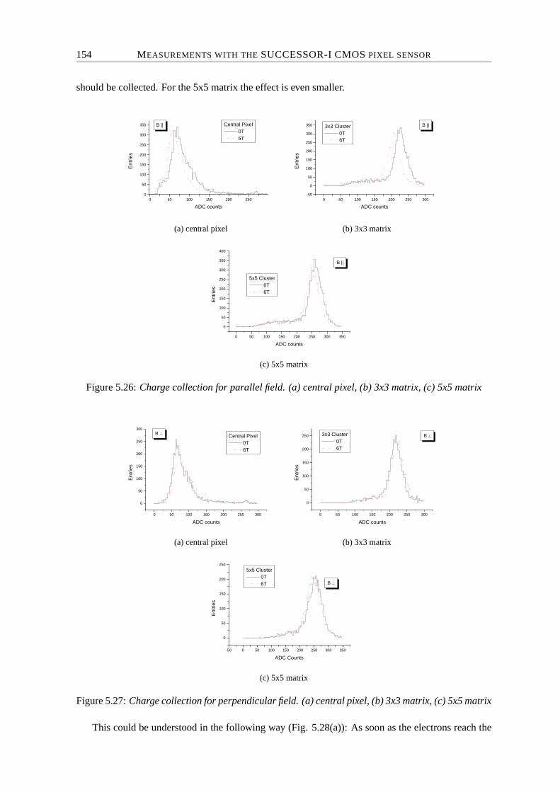
154 MEASUREMENTS WITH THE SUCCESSOR-I CMOS PIXEL SENSOR
should be collected. For the 5x5 matrix the effect is even smaller.
0 50 100 150 200 2500
50
100
150
200
250
300
350 B || Central Pixel0T6T
Ent
ries
ADC counts
(a) central pixel
0 50 100 150 200 250 300-50
0
50
100
150
200
250
300
350 3x3 Cluster0T6T
B ||
Ent
ries
ADC counts
(b) 3x3 matrix
0 50 100 150 200 250 300 350
0
50
100
150
200
250
300
350
400
B ||
5x5 Cluster0T6T
Ent
ries
ADC counts
(c) 5x5 matrix
Figure 5.26: Charge collection for parallel field. (a) central pixel, (b) 3x3 matrix, (c) 5x5 matrix
0 50 100 150 200 250 300
0
50
100
150
200
250
300
Central Pixel0T6T
B
Ent
ries
ADC counts
(a) central pixel
0 50 100 150 200 250 300
0
50
100
150
200
250 3x3 Cluster0T6T
B
Ent
ries
ADC counts
(b) 3x3 matrix
-50 0 50 100 150 200 250 300 350
0
50
100
150
200
250
B
5x5 Cluster0T6T
Ent
ries
ADC Counts
(c) 5x5 matrix
Figure 5.27: Charge collection for perpendicular field. (a) central pixel, (b) 3x3 matrix, (c) 5x5 matrix
This could be understood in the following way (Fig. 5.28(a)): As soon as the electrons reach the
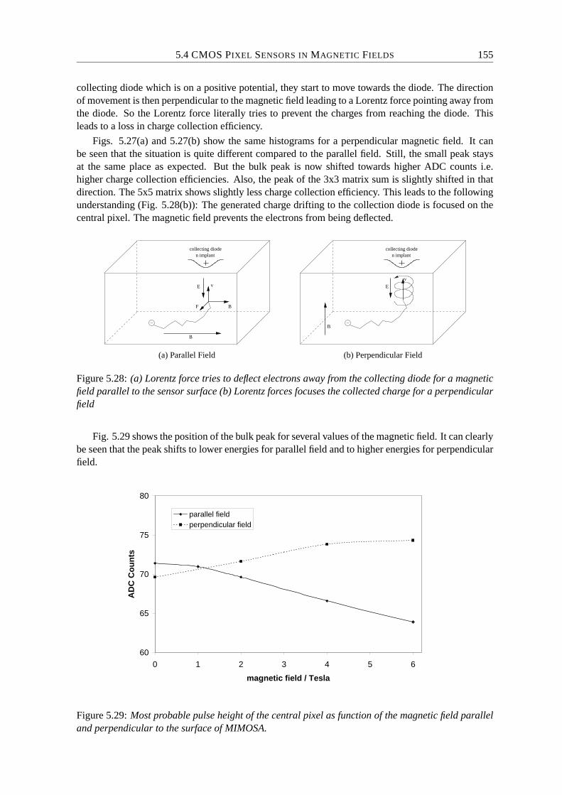
5.4 CMOS PIXEL SENSORS IN MAGNETIC FIELDS 155
collecting diode which is on a positive potential, they start to move towards the diode. The directionof movement is then perpendicular to the magnetic field leading to a Lorentz force pointing away fromthe diode. So the Lorentz force literally tries to prevent the charges from reaching the diode. Thisleads to a loss in charge collection efficiency.
Figs. 5.27(a) and 5.27(b) show the same histograms for a perpendicular magnetic field. It canbe seen that the situation is quite different compared to the parallel field. Still, the small peak staysat the same place as expected. But the bulk peak is now shifted towards higher ADC counts i.e.higher charge collection efficiencies. Also, the peak of the 3x3 matrix sum is slightly shifted in thatdirection. The 5x5 matrix shows slightly less charge collection efficiency. This leads to the followingunderstanding (Fig. 5.28(b)): The generated charge drifting to the collection diode is focused on thecentral pixel. The magnetic field prevents the electrons from being deflected.
B
v
F
n implantcollecting diode
E
B
(a) Parallel Field
n implantcollecting diode
B
E
v
(b) Perpendicular Field
Figure 5.28: (a) Lorentz force tries to deflect electrons away from the collecting diode for a magneticfield parallel to the sensor surface (b) Lorentz forces focuses the collected charge for a perpendicularfield
Fig. 5.29 shows the position of the bulk peak for several values of the magnetic field. It can clearlybe seen that the peak shifts to lower energies for parallel field and to higher energies for perpendicularfield.
60
65
70
75
80
0 1 2 3 4 5 6
magnetic field / Tesla
AD
CC
ou
nts
parallel fieldperpendicular field
Figure 5.29: Most probable pulse height of the central pixel as function of the magnetic field paralleland perpendicular to the surface of MIMOSA.
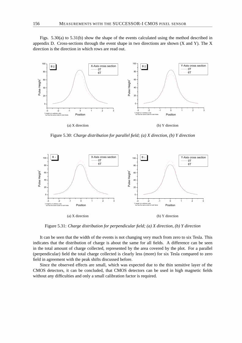
156 MEASUREMENTS WITH THE SUCCESSOR-I CMOS PIXEL SENSOR
Figs. 5.30(a) to 5.31(b) show the shape of the events calculated using the method described inappendix D. Cross-sections through the event shape in two directions are shown (X and Y). The Xdirection is the direction in which rows are read out.
(a) X direction (b) Y direction
Figure 5.30: Charge distribution for parallel field; (a) X direction, (b) Y direction
(a) X direction (b) Y direction
Figure 5.31: Charge distribution for perpendicular field; (a) X direction, (b) Y direction
It can be seen that the width of the events is not changing very much from zero to six Tesla. Thisindicates that the distribution of charge is about the same for all fields. A difference can be seenin the total amount of charge collected, represented by the area covered by the plot. For a parallel(perpendicular) field the total charge collected is clearly less (more) for six Tesla compared to zerofield in agreement with the peak shifts discussed before.
Since the observed effects are small, which was expected due to the thin sensitive layer of theCMOS detectors, it can be concluded, that CMOS detectors can be used in high magnetic fieldswithout any difficulties and only a small calibration factor is required.

Summary
In 2008 the Alpha Magnetic Spectrometer (AMS02) detector will be launched in a Space Shuttle to theInternational Space Station (ISS) and will then measure the spectrum of the primary cosmic rays, consist-ing of charged particles and photons, there for at least three years. During this time AMS02 will collect anunprecedented amount of data with an unrivalled precision in the energy range 300MeV to 3TeV. The analysisof this data will allow to refine the existing models for the acceleration and propagation of particles in the uni-verse. With the contribution of the Transition Radiation Detector (TRD) and the Electromagnetic Calorimeter,it will be possible to measure the positron fraction with very high precision, leading to a possible verification ofthe theories for the nature of the Dark Matter. The data of AMS02 will also be essential for any long durationmanned spaceflight outside of Earth’s protective environment, as it will, for the first time, allow to measure theflux of the primary particles as a function of the time for more than a few days.
The location of the AMS02 detector on the S3 truss of the ISS inflicts very stringent requirements onthe detector and electronic systems. The ability to withstand vacuum, temperature cycles on location andvibration during the transport in a Space Shuttle, but also the need to remain operational without any hardwaremaintenance, are among these requirements.
In the first part of this thesis the development of the electronics, from engineering level to pre-production,was discussed in detail using the example of the electronics for the TRD. This includes remarks on the generaldesign followed throughout the complete AMS02 experiment, like the redundancy in the system to overcomezero-maintenance issues, but also detector specific items like power schemes and data flow. In this presentationof the electronics (read out, slow-control and power distribution) an emphasis was put on the development ofthe firmware of the data reduction card (UDR) - detector specific part -, the low voltage regulator card (UPSFE)and the controller for the DC/DC converters (S9011AU), which were programmed within the framework of thisthesis.
In addition to the programming of the firmware codes for these cards, a test environment for the UPSFEhas been designed, built and successfully applied during the qualification of the pre-production at the Chung-Shan Institute of Science and Technology in Taiwan. In two test periods at the Proton Synchrotron (PS-T9)facility at CERN, the performance of the electronics was successfully tested with physics data taking usingdata acquisition systems consisting of electronics on the engineering (October 2002) and the qualification level(October 2003).
Additionally, it was shown, that the electronics of the TRD, at single board level, meet the requirements ofspace-qualified electronics by testing them in thermo-vacuum, vibration and electromagnetic interference tests.The integration and functionality tests at crate level at the Institut fur Experimentelle Kernphysik were finishedsuccessfully without showing any open issues. The space-qualification tests (thermo-vacuum test, vibrationtest and electro-magnetic interference test) will be done at crate level in the near future at the National SpaceProgram Office (NPSO) in Taiwan.
Dosimetry applications in brachytherapy, the local treatment of human tissue with high activity radioactivesources, and other applications, both in radiotherapy and High Energy Physics, call for detection devices with afine granularity and high tolerance with respect to the absorbed dose. Within the EU project “Silicon Ultra fastCameras for electron and gamma sources In Medical Applications” (SUCIMA) new prototype detectors weredeveloped based on CMOS and SOI technology. The SOI option was investigated by our colleagues in Cracowand found not to be mature enough yet for large scale applications.
In addition to the detectors, a USB2.0 data acquisition system was developed in the SUCIMA collaborationby our Cracow colleagues. Together with a LabView software developed in the framework of this thesis,it was used during the irradiations to create realistic scenarios and as well as for pre- and post-irradiationmeasurements, which were done to characterise the detectors.
The radiation hardness studies on a prototype CMOS pixel detector, the SUCCESSOR-I, were the othermain focus of this thesis and make up the second part of it. The SUCCESSOR-I detector was produced in the
157
158 SUMMARY
AMIS 0.35µm technology and has a 4µm epitaxial layer. Since the SUCCESSOR-I detector was designed asa technology study, its sensitive area is segmented into eight sub-matrices, each filled with pixels of a differentdesign. The purpose of the radiation hardness study was to find the pixel layout with the best compromise ofdetection efficiency and radiation tolerance.
The irradiations of the detectors were done using an X-ray system with a tungsten anode operating at anacceleration voltage of 60kV and a dose rate of ∼ 147krad/h, effectively limiting the damage effects of theradiation to charge trapping in the oxide. For all eight pixel types the most important characteristics weremeasured before and after the irradiation, which was done in steps of 500, 750 and 1000krad for chip #2 and1000 and 2000krad for chip #7.
As the main purpose of the radiation hardness studies was to choose the most robust pixel layout of theeight on SUCCESSOR-I, a number of figures of merit were selected: charge collection loss, intrinsic gain, gaindegradation, signal to noise ratio and leakage current.
While prototype CMOS detectors, measured in previous studies, showed serious degradation effects afterdoses of only 100krad [Dep02], it was proven for all eight pixel layouts of SUCCESSOR-I, that the chargecollection efficiency and the intrinsic gain of the pixels are only affected in a non-significant amount, evenfor doses of up to 2Mrad. Also the signal to noise ratio was quite stable and well above any critical value,especially at T = −15C, where the noise performance of the device is not so much affected by the increasedleakage current.
Thus the decision criteria were reduced to the gain of the pixel and the leakage current. The gain of thepixel should neither be too small (too little signal) nor be too high (limited dynamic range). The leakage currentof the pixel should be rather small, otherwise it would limit the maximum possible integration time, and shouldnot increase too much with the dose. The pixel matching these two criteria best is pixel 4, which is now alsoused in the final device of SUCIMA, the SUCCESSOR-V. Especially its leakage current behaviour is a big plus.The leakage current is much smaller than that of the other pixels and it only increases very slowly, by a factor18, with increasing dose (0krad to 2000krad). For comparison, the leakage current of pixel 3 increases for thesame dose by a factor of almost 660!
During the radiation hardness studies two effects were observed, which need to be addressed in futuredevices in order not to jeopardise the long term operation of a CMOS detector. The first item is the non-radiation hard digital part of SUCCESSOR-I. This is not a big problem, as solutions for this are already knownand have been proven to be successful. One remaining issue is the self-heating of the output buffers, whichincreases the leakage current of the pixels by rising their temperature and leads to inhomogeneous pedestals.This problem could be overcome by a modified layout of the output buffers, which is probably much quitedifficult to implement.
In addition to the radiation hardness measurements, also studies on the performance of CMOS pixel detec-tors under the influence of strong magnetic fields (≤ 6T ) were done using an older prototype CMOS detector,MIMOSA-I. Two sets of measurements were performed. In the first set the detector surface was aligned parallelto the magnetic field, in the second perpendicular to it. While for the first set the signal becomes weaker withincreasing field strength, it becomes stronger in the second case. The smallness of these effects was expected,as the sensitive volume of CMOS sensors is very thin. The current understanding of this effect is based on theLorentz force, that deflects drifting charges in magnetic fields. In the first case the Lorentz force results in alonger effective drift path hindering the electrons from reaching the collecting diode within the integration time.In the second case, the Lorentz force acts against movements away from the collecting diode and thus bringsmore electrons to the collecting diode.
As a summary it can be said, that a radiation hard CMOS detector was successfully developed together witha corresponding USB2.0 DAQ card. This system can be understood as a digital camera for ionising radiation,that can be easily connected to any standard PC. A system using the SUCCESSOR-V as detection device willbe able to make more than 10000 measurements under worst case conditions (measurement time: 10s, doserate: 20rad/s). Older designs would only last a few hundred measurements, as their performance, especiallythe charge collection efficiency, degraded very fast with increasing dose.

Appendix A
LeCroy Bus data word definition
LeCroy OUT LeCroy IN
bit function internal use bit function0 1 32 01 parity bit (odd) 33 echo of parity bit2 power down bit unused 34 echo of power down bit3 broadcast bit unused 35 echo of broadcast bit4 select code [7] board address [3] 36 echo of select code [7]5 select code [6] board address [2] 37 echo of select code [6]6 select code [5] board address [1] 38 echo of select code [5]7 select code [4] board address [0] 39 echo of select code [4]8 select code [3] unused 40 echo of select code [3]9 select code [2] unused 41 echo of select code [2]10 select code [1] unused 42 echo of select code [1]11 select code [0] register address [3] 43 echo of select code [0]12 read/write 44 echo of read/write13 section address [2] register address [2] 45 echo of section address [2]14 section address [1] register address [1] 46 echo of section address [1]15 section address [0] register address [0] 47 echo of section address [0]16 data [15] 48 data [15]17 data [14] 49 data [14]18 data [13] 50 data [13]19 data [12] 51 data [12]20 data [11] 52 data [11]21 data [10] 53 data [10]22 data [9] 54 data [9]23 data [8] 55 data [8]24 data [7] 56 data [7]25 data [6] 57 data [6]26 data [5] 58 data [5]27 data [4] 59 data [4]28 data [3] 60 data [3]29 data [2] 61 data [2]30 data [1] 62 data [1]31 data [0] 63 data [0]
Table A.1: LeCroy bus bit function.

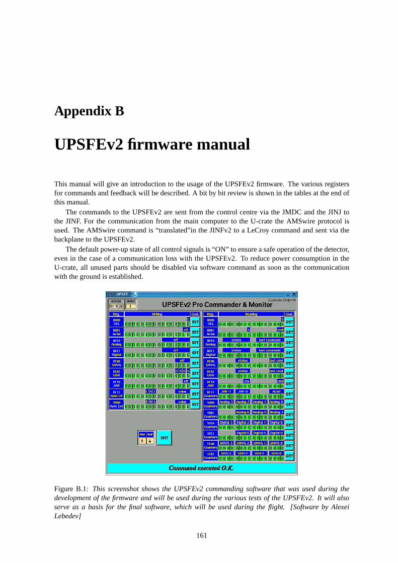
Appendix B
UPSFEv2 firmware manual
This manual will give an introduction to the usage of the UPSFEv2 firmware. The various registersfor commands and feedback will be described. A bit by bit review is shown in the tables at the end ofthis manual.
The commands to the UPSFEv2 are sent from the control centre via the JMDC and the JINJ tothe JINF. For the communication from the main computer to the U-crate the AMSwire protocol isused. The AMSwire command is “translated”in the JINFv2 to a LeCroy command and sent via thebackplane to the UPSFEv2.
The default power-up state of all control signals is “ON” to ensure a safe operation of the detector,even in the case of a communication loss with the UPSFEv2. To reduce power consumption in theU-crate, all unused parts should be disabled via software command as soon as the communicationwith the ground is established.
Figure B.1: This screenshot shows the UPSFEv2 commanding software that was used during thedevelopment of the firmware and will be used during the various tests of the UPSFEv2. It will alsoserve as a basis for the final software, which will be used during the flight. [Software by AlexeiLebedev]
161
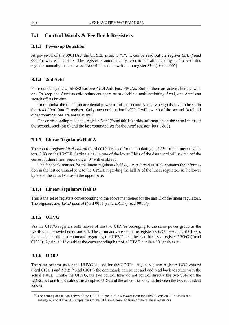
162 UPSFEV2 FIRMWARE MANUAL
B.1 Control Words & Feedback Registers
B.1.1 Power-up Detection
At power-on of the S9011AU the bit SEL is set to “1”. It can be read out via register SEL (“read0000”), where it is bit 0. The register is automatically reset to “0” after reading it. To reset thisregister manually the data word “x0001” has to be written to register SEL (“ctrl 0000”).
B.1.2 2nd Actel
For redundancy the UPSFEv2 has two Actel Anti-Fuse FPGAs. Both of them are active after a power-on. To keep one Actel as cold redundant spare or to disable a malfunctioning Actel, one Actel canswitch off its brother.
To minimise the risk of an accidental power-off of the second Actel, two signals have to be set inthe Actel (“crtl 0001”) register. Only one combination “x0001” will switch of the second Actel, allother combinations are not relevant.
The corresponding feedback register Actel (“read 0001”) holds information on the actual status ofthe second Actel (bit 8) and the last command set for the Actel register (bits 1 & 0).
B.1.3 Linear Regulators Half A
The control register LR A control (“crtl 0010”) is used for manipulating half A(1) of the linear regula-tors (LR) on the UPSFE. Setting a “1” in one of the lower 7 bits of the data word will switch off thecorresponding linear regulator, a “0” will enable it.
The feedback register for the linear regulators half A, LR A (“read 0010”), contains the informa-tion in the last command sent to the UPSFE regarding the half A of the linear regulators in the lowerbyte and the actual status in the upper byte.
B.1.4 Linear Regulators Half D
This is the set of registers corresponding to the above mentioned for the half D of the linear regulators.The registers are: LR D control (“crtl 0011”) and LR D (“read 0011”).
B.1.5 UHVG
Via the UHVG registers both halves of the two UHVGs belonging to the same power group as theUPSFE can be switched on and off. The commands are set in the register UHVG control (“crtl 0100”),the status and the last command regarding the UHVGs can be read back via register UHVG (“read0100”). Again, a “1” disables the corresponding half of a UHVG, while a “0” enables it.
B.1.6 UDR2
The same scheme as for the UHVG is used for the UDR2s. Again, via two registers UDR control(“crtl 0101”) and UDR (“read 0101”) the commands can be set and and read back together with theactual status. Unlike the UHVG, the two control lines do not control directly the two SSFs on theUDRs, but one line disables the complete UDR and the other one switches between the two redundanthalves.
(1)The naming of the two halves of the UPSFE A and D is a left-over from the UPSFE version 1, in which theanalog (A) and digital (D) supply lines to the UFE were powered from different linear regulators.
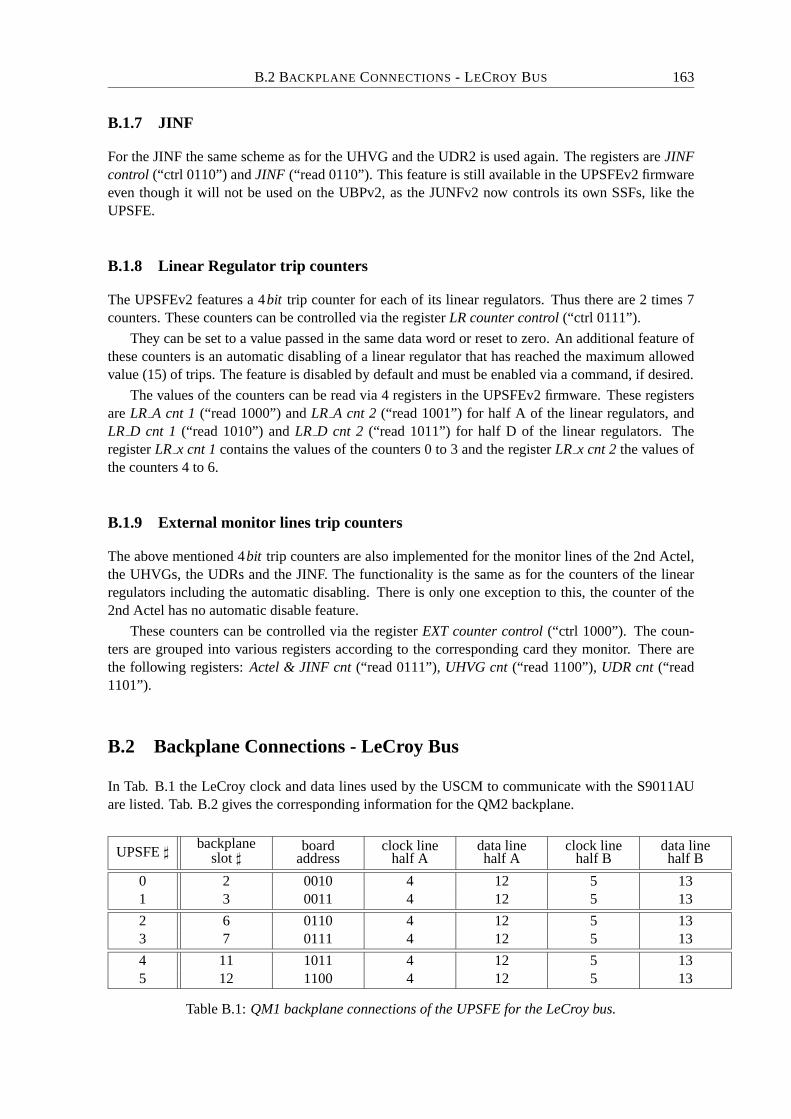
B.2 BACKPLANE CONNECTIONS - LECROY BUS 163
B.1.7 JINF
For the JINF the same scheme as for the UHVG and the UDR2 is used again. The registers are JINFcontrol (“ctrl 0110”) and JINF (“read 0110”). This feature is still available in the UPSFEv2 firmwareeven though it will not be used on the UBPv2, as the JUNFv2 now controls its own SSFs, like theUPSFE.
B.1.8 Linear Regulator trip counters
The UPSFEv2 features a 4bit trip counter for each of its linear regulators. Thus there are 2 times 7counters. These counters can be controlled via the register LR counter control (“ctrl 0111”).
They can be set to a value passed in the same data word or reset to zero. An additional feature ofthese counters is an automatic disabling of a linear regulator that has reached the maximum allowedvalue (15) of trips. The feature is disabled by default and must be enabled via a command, if desired.
The values of the counters can be read via 4 registers in the UPSFEv2 firmware. These registersare LR A cnt 1 (“read 1000”) and LR A cnt 2 (“read 1001”) for half A of the linear regulators, andLR D cnt 1 (“read 1010”) and LR D cnt 2 (“read 1011”) for half D of the linear regulators. Theregister LR x cnt 1 contains the values of the counters 0 to 3 and the register LR x cnt 2 the values ofthe counters 4 to 6.
B.1.9 External monitor lines trip counters
The above mentioned 4bit trip counters are also implemented for the monitor lines of the 2nd Actel,the UHVGs, the UDRs and the JINF. The functionality is the same as for the counters of the linearregulators including the automatic disabling. There is only one exception to this, the counter of the2nd Actel has no automatic disable feature.
These counters can be controlled via the register EXT counter control (“ctrl 1000”). The coun-ters are grouped into various registers according to the corresponding card they monitor. There arethe following registers: Actel & JINF cnt (“read 0111”), UHVG cnt (“read 1100”), UDR cnt (“read1101”).
B.2 Backplane Connections - LeCroy Bus
In Tab. B.1 the LeCroy clock and data lines used by the USCM to communicate with the S9011AUare listed. Tab. B.2 gives the corresponding information for the QM2 backplane.
UPSFE backplane
slot board
addressclock line
half Adata linehalf A
clock linehalf B
data linehalf B
0 2 0010 4 12 5 131 3 0011 4 12 5 13
2 6 0110 4 12 5 133 7 0111 4 12 5 13
4 11 1011 4 12 5 135 12 1100 4 12 5 13
Table B.1: QM1 backplane connections of the UPSFE for the LeCroy bus.
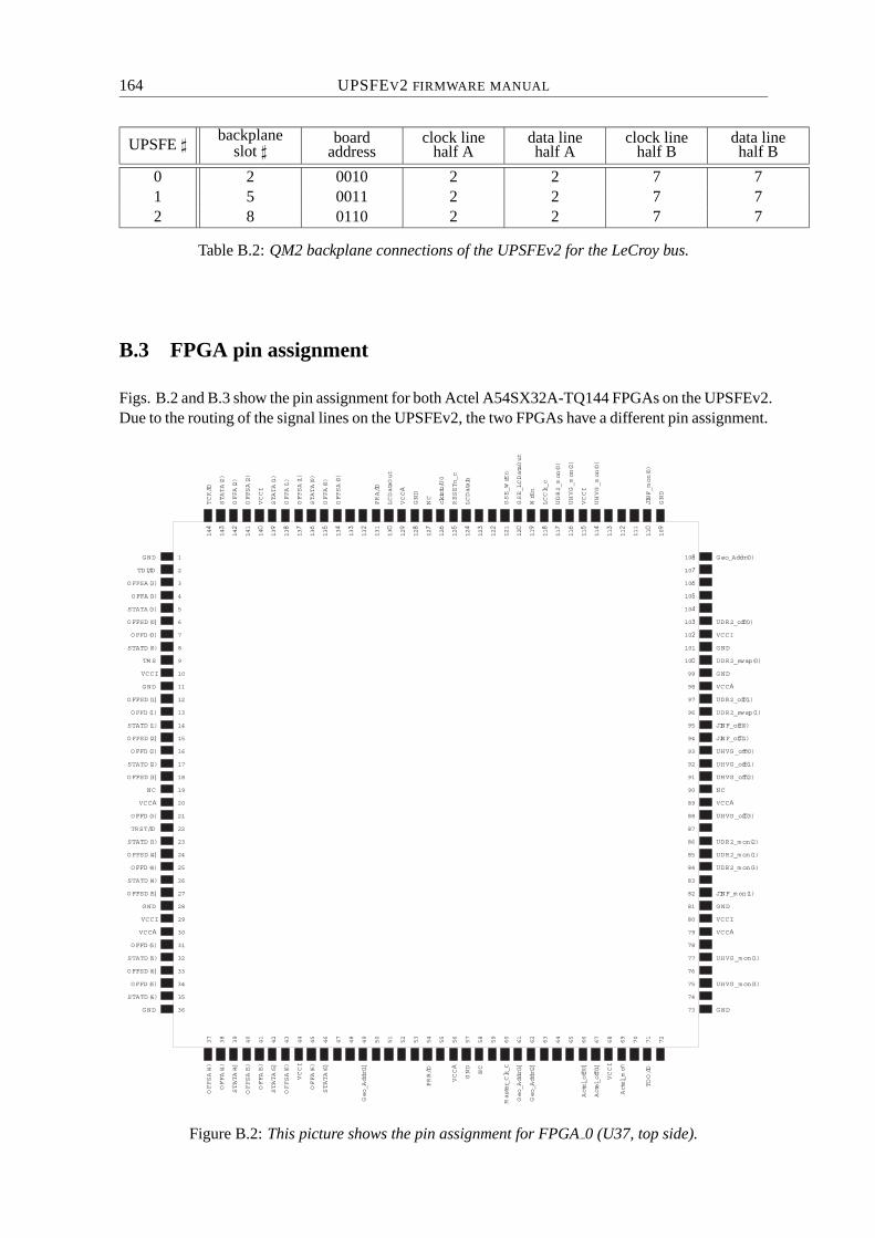
164 UPSFEV2 FIRMWARE MANUAL
UPSFE backplane
slot board
addressclock line
half Adata linehalf A
clock linehalf B
data linehalf B
0 2 0010 2 2 7 71 5 0011 2 2 7 72 8 0110 2 2 7 7
Table B.2: QM2 backplane connections of the UPSFEv2 for the LeCroy bus.
B.3 FPGA pin assignment
Figs. B.2 and B.3 show the pin assignment for both Actel A54SX32A-TQ144 FPGAs on the UPSFEv2.Due to the routing of the signal lines on the UPSFEv2, the two FPGAs have a different pin assignment.
1G ND
2TDI/IO
3OFFSA(3)
4O FFA(3)
5STATA(3)
6OFFSD(0
7OFFD(0)
8STATD(0)
9TM S
10VCCI
11G ND
12OFFSD(1
13OFFD(1)
14STATD(1)
15OFFSD(2
16OFFD(2)
17STATD(2)
18OFFSD(3
19NC
20VCC
21OFFD(3)
22TRST/IO
23STATD(3)
24OFFSD(4
25OFFD(4)
26STATD(4)
27OFFSD(5
28G ND
29VCCI
30VCC
31OFFD(5)
32STATD(5)
33OFFSD(6
34OFFD(6)
35STATD(6)
36G ND
10 G eo_Addr(0)
10
10
10
10
10 UDR2_off(0)
10 VCCI
101 G ND
10 UDR2_swap(0)
99 G ND
98 VCC
97 UDR2_off(1)
96 UDR2_swap(1)
95 JINF_off(0)
94 JINF_off(1)
93 UHVG _off(0)
92 UHVG _off(1)
91 UHVG _off(2)
90 NC
89 VCC
88 UHVG _off(3)
87
86 UDR2_m on(2)
85 UDR2_m on(1)
84 UDR2_m on(3)
83
82 JINF_m on(1)
81 G ND
80 VCCI
79 VCC
78
77 UHVG _m on(1)
76
75 UHVG _m on(3)
74
73 G ND
14
TCK/IO
14
STATA(2)
14
OFFA(2)
141
OFFSA(2)
14
VCCI
13
STATA(1)
13
OFFA(1)
13
OFFSA(1)
13
STATA(0)
13
OFFA(0)
13
OFFSA(0)
13
13
131
PRA/IO
13
LCDataOut
12
VCC
12
GND
12
NC
12
clkintb/U0
12
RESETn_c
12
LCDataIn
12
12
121
GSE_WrEn
12
GSE_LCDataOut
11
WrEn
11
LCClk_c
11
UDR2_mon(0)
11
UHVG_mon(2)
11
VCCI
11
UHVG_mon(0)
11
11
111
11
JINF_mon(0)
10
GND
37
OFFSA(4)
38
OFFA(4)
39
STATA(4
40
OFFSA(5)
41
OFFA(5)
42
STATA(5
43
OFFSA(6)
44
VCCI
45
OFFA(6)
46
STATA(6
47
48
49
Geo_Addr(1
50
51
52
53
54
PRB/IO
55
56
VCC
57
GND
58
NC
59
60
Master_Clk_
61
Geo_Addr(3
62
Geo_Addr(2
63
64
65
66
Actel_off(0
67
Actel_off(1
68
VCCI
69
Actel_mo
70
71
TDO/IO
72
Figure B.2: This picture shows the pin assignment for FPGA 0 (U37, top side).
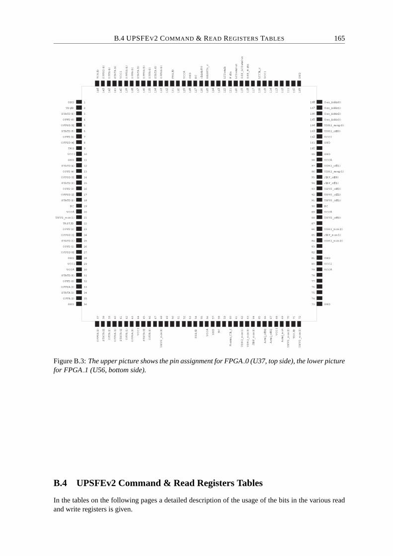
B.4 UPSFEV2 COMMAND & READ REGISTERS TABLES 165
1G ND
2TDI/IO
3STATD(6)
4OFFD(6)
5OFFSD(5
6STATD(5)
7OFFD(5)
8OFFSD(4
9TM S
10VCCI
11G ND
12STATD(4)
13OFFD(4)
14OFFSD(3
15STATD(3)
16OFFD(3)
17OFFSD(2
18STATD(2)
19NC
20VCC
21UHVG_m on(1)
22TRST/IO
23OFFD(2)
24OFFSD(1
25STATD(1)
26OFFD(1)
27OFFSD(0
28G ND
29VCCI
30VCC
31STATD(0)
32OFFD(0)
33OFFSA(3)
34STATA(3)
35O FFA(3)
36G ND
10 G eo_Addr(0)
10 G eo_Addr(1)
10 G eo_Addr(2)
10 G eo_Addr(3)
10 UDR2_swap(0)
10 UDR2_off(0)
10 VCCI
101 G ND
10
99 G ND
98 VCC
97 UDR2_off(1)
96 UDR2_swap(1)
95 JINF_off(0)
94 JINF_off(1)
93 UHVG _off(3)
92 UHVG _off(2)
91 UHVG _off(1)
90 NC
89 VCC
88 UHVG _off(0)
87
86 UDR2_m on(2)
85 JINF_m on(1)
84 UDR2_m on(3)
83
82
81 G ND
80 VCCI
79 VCC
78
77
76
75
74
73 G ND
14
TCK/IO
14
OFFSD(6)
14
OFFA(4)
141
STATA(4)
14
VCCI
13
OFFSA(4)
13
OFFA(5)
13
STATA(5)
13
OFFSA(5)
13
OFFA(6)
13
STATA(6)
13
OFFSA(6)
13
131
PRA/IO
13
12
VCC
12
GND
12
NC
12
clkintb/U0
12
RESETn_c
12
12
12
LCDataIn
121
WrEn
12
LCDataOut
11
GSE_LCDataOut
11
GSE_WrEn
11
11
LCClk_c
11
VCCI
11
11
11
111
11
10
GND
37
OFFSA(2)
38
STATA(2
39
OFFA(2)
40
OFFSA(1)
41
STATA(1
42
OFFA(1)
43
OFFSA(0)
44
VCCI
45
STATA(0
46
OFFA(0)
47
48
UHVG_mon(0)
49
50
51
52
53
54
PRB/IO
55
56
VCC
57
GND
58
NC
59
60
Master_Clk_
61
62
UDR2_mon(1)
63
UDR2_mon(0)
64
JINF_mon(0)
65
66
Actel_off(0
67
Actel_off(1
68
VCCI
69
Actel_mo
70
UHVG_mon(2)
71
TDO/IO
72
UHVG_mon(3)
Figure B.3: The upper picture shows the pin assignment for FPGA 0 (U37, top side), the lower picturefor FPGA 1 (U56, bottom side).
B.4 UPSFEv2 Command & Read Registers Tables
In the tables on the following pages a detailed description of the usage of the bits in the various readand write registers is given.

166 UPSFEV2 FIRMWARE MANUAL
register0000
00010010
00110100
01010110
01111000
name
SEL
Actel
controlL
RA
controlL
RD
controlU
HV
Gcontrol
UD
Rcontrol
JINF
controlL
Rcounter
controlE
XT
countercontrol
data[15]
00
00
00
00
0
data[14]
00
00
00
00
0
data[13]
00
00
00
00
0
data[12]
00
00
00
00
0
data[11]
00
00
00
00
0
data[10]
00
00
00
0enable
autom
odeenable
autom
ode
data[9]
00
00
00
0resetL
Rcounter
resetEX
Tcounter
data[8]
00
00
00
0load
LR
counterload
EX
Tcounter
data[7]
00
00
00
00
0
data[6]
00
LR
Aoff
[6]L
RD
off[6]
00
00
0
data[5]
00
LR
Aoff
[5]L
RD
off[5]
00
00
0
data[4]
00
LR
Aoff
[4]L
RD
off[4]
00
00
0
data[3]
00
LR
Aoff
[3]L
RD
off[3]
UH
VG
off[3]
UD
Roff
[1]0
valueL
R[3]
valueE
XT
[3]
data[2]
00
LR
Aoff
[2]L
RD
off[2]
UH
VG
off[2]
UD
Rsw
ap[1]
0value
LR
[2]value
EX
T[2]
data[1]
0A
cteloff[1]
LR
Aoff
[1]L
RD
off[1]
UH
VG
off[1]
UD
Roff
[0]JIN
Foff
[1]value
LR
[1]value
EX
T[1]
data[0]
clearSE
LA
cteloff[0]
LR
Aoff
[0]L
RD
off[0]
UH
VG
off[0]
UD
Rsw
ap[0]
JINF
off[0]
valueL
R[0]
valueE
XT
[0]
TableB
.3:U
PSF
Ev2
write
comm
ands.T
hedata
bits0..15
correspondto
bits16..31
inTab.
A.1.
Ifa“
1”is
loadedin
toa
registerthe
correspondingdevice
isdisabled.
Toenable
it,loada
“0”
intoit.
Are
more
detaileddescription
isgiven
inthe
sectionscorresponding
tothe
registerson
thepreceding
pages.
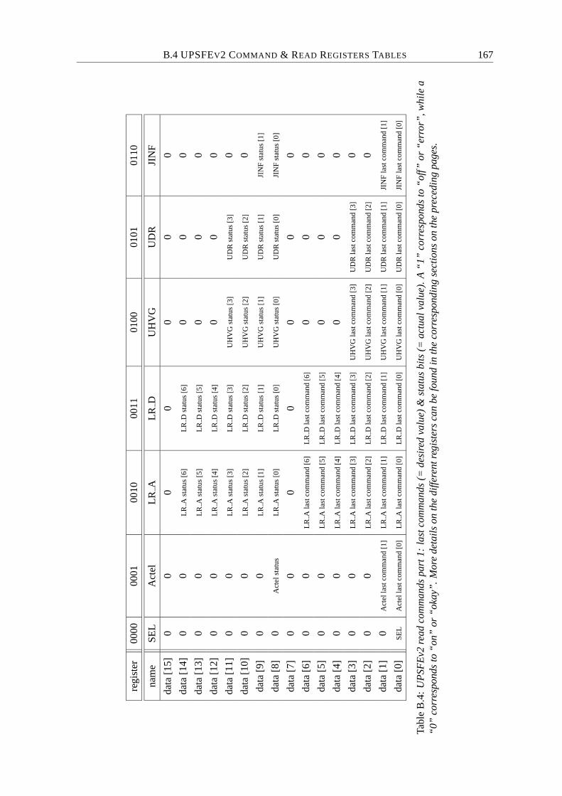
B.4 UPSFEV2 COMMAND & READ REGISTERS TABLES 167
regi
ster
0000
0001
0010
0011
0100
0101
0110
nam
eSE
LA
ctel
LR
AL
RD
UH
VG
UD
RJI
NF
data
[15]
00
00
00
0
data
[14]
00
LR
Ast
atus
[6]
LR
Dst
atus
[6]
00
0
data
[13]
00
LR
Ast
atus
[5]
LR
Dst
atus
[5]
00
0
data
[12]
00
LR
Ast
atus
[4]
LR
Dst
atus
[4]
00
0
data
[11]
00
LR
Ast
atus
[3]
LR
Dst
atus
[3]
UH
VG
stat
us[3
]U
DR
stat
us[3
]0
data
[10]
00
LR
Ast
atus
[2]
LR
Dst
atus
[2]
UH
VG
stat
us[2
]U
DR
stat
us[2
]0
data
[9]
00
LR
Ast
atus
[1]
LR
Dst
atus
[1]
UH
VG
stat
us[1
]U
DR
stat
us[1
]JI
NF
stat
us[1
]
data
[8]
0A
ctel
stat
usL
RA
stat
us[0
]L
RD
stat
us[0
]U
HV
Gst
atus
[0]
UD
Rst
atus
[0]
JIN
Fst
atus
[0]
data
[7]
00
00
00
0
data
[6]
00
LR
Ala
stco
mm
and
[6]
LR
Dla
stco
mm
and
[6]
00
0
data
[5]
00
LR
Ala
stco
mm
and
[5]
LR
Dla
stco
mm
and
[5]
00
0
data
[4]
00
LR
Ala
stco
mm
and
[4]
LR
Dla
stco
mm
and
[4]
00
0
data
[3]
00
LR
Ala
stco
mm
and
[3]
LR
Dla
stco
mm
and
[3]
UH
VG
last
com
man
d[3
]U
DR
last
com
man
d[3
]0
data
[2]
00
LR
Ala
stco
mm
and
[2]
LR
Dla
stco
mm
and
[2]
UH
VG
last
com
man
d[2
]U
DR
last
com
man
d[2
]0
data
[1]
0A
ctel
last
com
man
d[1
]L
RA
last
com
man
d[1
]L
RD
last
com
man
d[1
]U
HV
Gla
stco
mm
and
[1]
UD
Rla
stco
mm
and
[1]
JIN
Fla
stco
mm
and
[1]
data
[0]
SEL
Act
ella
stco
mm
and
[0]
LR
Ala
stco
mm
and
[0]
LR
Dla
stco
mm
and
[0]
UH
VG
last
com
man
d[0
]U
DR
last
com
man
d[0
]JI
NF
last
com
man
d[0
]
Tabl
eB
.4:
UP
SFE
v2re
adco
mm
ands
part
1:la
stco
mm
ands
(=de
sire
dva
lue)
&st
atus
bits
(=ac
tual
valu
e).
A“
1”co
rres
pond
sto
“of
f”or
“er
ror”
,whi
lea
“0”
corr
espo
nds
to“
on”
or“
okay
”.
Mor
ede
tail
son
the
diffe
rent
regi
ster
sca
nbe
foun
din
the
corr
espo
ndin
gse
ctio
nson
the
prec
edin
gpa
ges.

168 UPSFEV2 FIRMWARE MANUAL
register0111
10001001
10101011
11001101
name
Actel&
JINF
cntL
RA
cnt1L
RA
cnt2L
RD
cnt1L
RD
cnt2U
HV
Gcnt
UD
R
data[15]
JINF
counter1
[3]L
RA
counter3
[3]0
LR
Dcounter
3[3]
0U
HV
Gcounter
3[3]
UD
Rcounter
3[3]
data[14]
JINF
counter1
[2]L
RA
counter3
[2]0
LR
Dcounter
3[2]
0U
HV
Gcounter
3[2]
UD
Rcounter
3[2]
data[13]
JINF
counter1
[1]L
RA
counter3
[1]0
LR
Dcounter
3[1]
0U
HV
Gcounter
3[1]
UD
Rcounter
3[1]
data[12]
JINF
counter1
[0]L
RA
counter3
[0]0
LR
Dcounter
3[0]
0U
HV
Gcounter
3[0]
UD
Rcounter
3[0]
data[11]
JINF
counter0
[3]L
RA
counter2
[3]L
RA
counter6
[3]L
RD
counter2
[3]L
RD
counter6
[3]U
HV
Gcounter
2[3]
UD
Rcounter
2[3]
data[10]
JINF
counter0
[2]L
RA
counter2
[2]L
RA
counter6
[2]L
RD
counter2
[2]L
RD
counter6
[2]U
HV
Gcounter
2[2]
UD
Rcounter
2[2]
data[9]
JINF
counter0
[1]L
RA
counter2
[1]L
RA
counter6
[1]L
RD
counter2
[1]L
RD
counter6
[1]U
HV
Gcounter
2[1]
UD
Rcounter
2[1]
data[8]
JINF
counter0
[0]L
RA
counter2
[0]L
RA
counter6
[0]L
RD
counter2
[0]L
RD
counter6
[0]U
HV
Gcounter
2[0]
UD
Rcounter
2[0]
data[7]
0L
RA
counter1
[3]L
RA
counter5
[3]L
RD
counter1
[3]L
RD
counter5
[3]U
HV
Gcounter
1[3]
UD
Rcounter
1[3]
data[6]
0L
RA
counter1
[2]L
RA
counter5
[2]L
RD
counter1
[2]L
RD
counter5
[2]U
HV
Gcounter
1[2]
UD
Rcounter
1[2]
data[5]
0L
RA
counter1
[1]L
RA
counter5
[1]L
RD
counter1
[1]L
RD
counter5
[1]U
HV
Gcounter
1[1]
UD
Rcounter
1[1]
data[4]
0L
RA
counter1
[0]L
RA
counter5
[0]L
RD
counter1
[0]L
RD
counter5
[0]U
HV
Gcounter
1[0]
UD
Rcounter
1[0]
data[3]
Actelcounter
[3]L
RA
counter0
[3]L
RA
counter4
[3]L
RD
counter0
[3]L
RD
counter4
[3]U
HV
Gcounter
0[3]
UD
Rcounter
0[3]
data[2]
Actelcounter
[2]L
RA
counter0
[2]L
RA
counter4
[2]L
RD
counter0
[2]L
RD
counter4
[2]U
HV
Gcounter
0[2]
UD
Rcounter
0[2]
data[1]
Actelcounter
[1]L
RA
counter0
[1]L
RA
counter4
[1]L
RD
counter0
[1]L
RD
counter4
[1]U
HV
Gcounter
0[1]
UD
Rcounter
0[1]
data[0]
Actelcounter
[0]L
RA
counter0
[0]L
RA
counter4
[0]L
RD
counter0
[0]L
RD
counter4
[0]U
HV
Gcounter
0[0]
UD
Rcounter
0[0]
TableB
.5:U
PSF
Ev2
readcom
mands
part2:trip
counters.T
heregisters
containthe
valuesofthe
tripcounters
ofthem
onitorlines
fromthe
linearregulators
andthe
externalmonitor
lines.For
more
detailsplease
referto
thecorresponding
sectionson
thepreceding
pages.
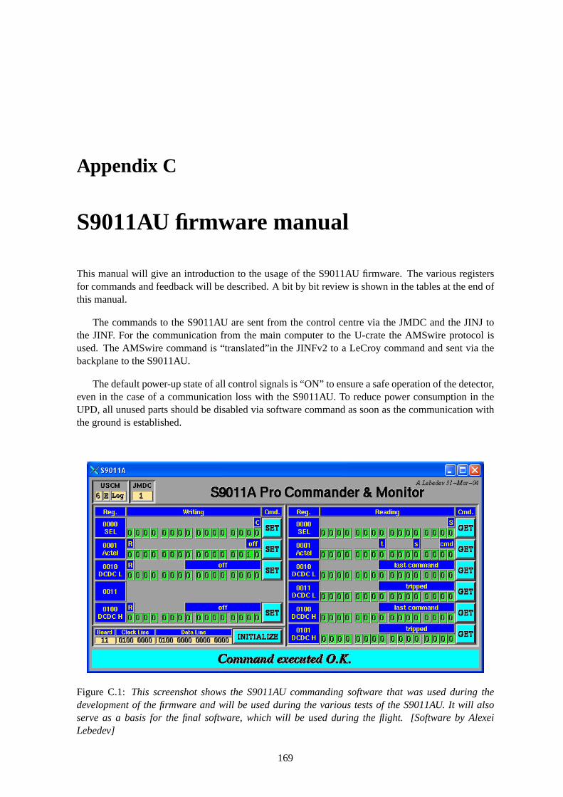
Appendix C
S9011AU firmware manual
This manual will give an introduction to the usage of the S9011AU firmware. The various registersfor commands and feedback will be described. A bit by bit review is shown in the tables at the end ofthis manual.
The commands to the S9011AU are sent from the control centre via the JMDC and the JINJ tothe JINF. For the communication from the main computer to the U-crate the AMSwire protocol isused. The AMSwire command is “translated”in the JINFv2 to a LeCroy command and sent via thebackplane to the S9011AU.
The default power-up state of all control signals is “ON” to ensure a safe operation of the detector,even in the case of a communication loss with the S9011AU. To reduce power consumption in theUPD, all unused parts should be disabled via software command as soon as the communication withthe ground is established.
Figure C.1: This screenshot shows the S9011AU commanding software that was used during thedevelopment of the firmware and will be used during the various tests of the S9011AU. It will alsoserve as a basis for the final software, which will be used during the flight. [Software by AlexeiLebedev]
169

170 S9011AU FIRMWARE MANUAL
C.1 Command & Feedback Registers
C.1.1 Power-up Detection
At power-on of the S9011AU the bit SEL is set to “1”. It can be read out via register SEL (“read0000”), where it is bit 0. The register is automatically reset to “0” after reading it. To reset thisregister manually the data word “x0001” has to be written to register SEL (“ctrl 0000”).
C.1.2 2nd Actel
For redundancy the S9011AU has two Actel Anti-Fuse FPGAs. Both of them are active after a power-on. To keep one Actel as cold redundant spare or to disable a malfunctioning Actel, one Actel canswitch off its brother.
To minimise the risk of an accidental power-off of the second Actel, two signals have to be set inthe Actel (“crtl 0001”) register. Only one combination “x0001” will switch of the second Actel, allother combinations are not relevant.
The corresponding feedback register Actel (“read 0001”) holds information on the actual statusof the second Actel (bit 8), the trip detection flip-flop (bit 4) and the last command set for the Actelregister (bits 1 & 0).
C.1.3 DC/DC converters half L
The control register DC/DC L (“crtl 0010”) is used for manipulating the L half of the DC/DC con-verters in the UPD. Setting a “1” in one of the lower 9 bits of the data word will switch off thecorresponding DC/DC converter, a “0” will enable it.
There are two feedback registers for the DC/DC converter halves L. The first one, DC/DC L lastcommand (“read 0010”), contains the information in the last command sent to the S9011AU regardingthe L halves of the DC/DC converters. The second register, DC/DC L trip FFs (“read 0011”) allowsto read the trip detection flip-flops for the 9 L halves.
C.1.4 DC/DC converters half H
This is the set of registers corresponding to the above mentioned for the H halves of the DC/DCconverters. The registers are: DC/DC H (“crtl 0100”), DC/DC H last command (“read 0100”) andDC/DC H trip FFs (“read 0101”).
C.2 Backplane Connections - LeCroy Bus
In Tab. C.1 the LeCroy clock and data lines used by the USCM to communicate with the S9011AUare listed. Tab. C.2 gives the corresponding information for the QM2 backplane.
S9011AU boardaddress
clock linehalf A
data linehalf A
clock linehalf B
data linehalf B
0 0011 6 14 7 15
Table C.1: QM1 Backplane Connections of the S9011AU for the LeCroy Bus.
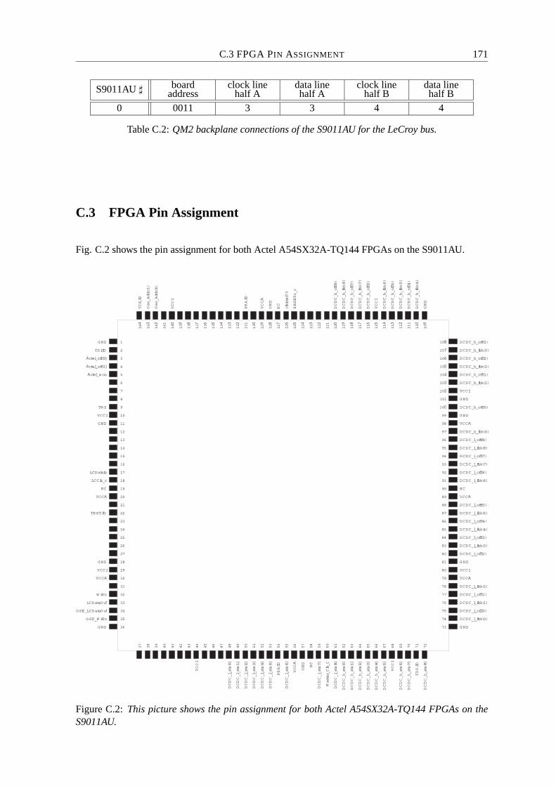
C.3 FPGA PIN ASSIGNMENT 171
S9011AU boardaddress
clock linehalf A
data linehalf A
clock linehalf B
data linehalf B
0 0011 3 3 4 4
Table C.2: QM2 backplane connections of the S9011AU for the LeCroy bus.
C.3 FPGA Pin Assignment
Fig. C.2 shows the pin assignment for both Actel A54SX32A-TQ144 FPGAs on the S9011AU.
1G ND
2TDI/IO
3ctel_off(0
4ctel_off(1
5ctel_m on
6
7
8
9TM S
10VCCI
11G ND
12
13
14
15
16
17LCDataIn
18LCClk_c
19NC
20VCC
21
22TRST/IO
23
24
25
26
27
28G ND
29VCCI
30VCC
31
32W rEn
33LCDataO u
34GSE_LCDataOu
35G SE_W rEn
36G ND
10 DCDC_h_off(3)
10 DCDC_h_fbk(3)
10 DCDC_h_off(2)
10 DCDC_h_fbk(2)
10 DCDC_h_off(1)
10 DCDC_h_fbk(1)
10 VCCI
101 G ND
10 DCDC_h_off(0)
99 G ND
98 VCC
97 DCDC_h_fbk(0)
96 DCDC_l_off(8)
95 DCDC_l_fbk(8)
94 DCDC_l_off(7)
93 DCDC_l_fbk(7)
92 DCDC_l_off(6)
91 DCDC_l_fbk(6)
90 NC
89 VCC
88 DCDC_l_off(5)
87 DCDC_l_fbk(5)
86 DCDC_l_off(4)
85 DCDC_l_fbk(4)
84 DCDC_l_off(3)
83 DCDC_l_fbk(3)
82 DCDC_l_off(2)
81 G ND
80 VCCI
79 VCC
78 DCDC_l_fbk(2)
77 DCDC_l_off(1)
76 DCDC_l_fbk(1)
75 DCDC_l_off(0)
74 DCDC_l_fbk(0)
73 G ND
14
TCK/IO
14
Geo_Addr(1)
14
Geo_Addr(0)
141
14
VCCI
13
13
13
13
13
13
13
13
131
PRA/IO
13
12
VCC
12
GND
12
NC
12
clkinta/U0
12
RESETn_c
12
12
12
121
12
DCDC_h_off(8)
11
DCDC_h_fbk(8)
11
DCDC_h_off(7)
11
DCDC_h_fbk(7)
11
DCDC_h_off(6)
11
VCCI
11
DCDC_h_fbk(6)
11
DCDC_h_off(5)
11
DCDC_h_fbk(5)
111
DCDC_h_off(4)
11
DCDC_h_fbk(4)
10
GND
37
38
39
40
41
42
43
44
VCCI
45
46
47
48
DCDC_l_sts(0
49
DCDC_l_sts(1
50
DCDC_l_sts(2
51
DCDC_l_sts(3
52
DCDC_l_sts(4
53
DCDC_l_sts(5
54
PRB/IO
55
DCDC_l_sts(6
56
VCC
57
GND
58
NC
59
DCDC_l_sts(7
60
Master_Clk_
61
DCDC_l_sts(8
62
DCDC_h_sts(0
63
DCDC_h_sts(1
64
DCDC_h_sts(2
65
DCDC_h_sts(3
66
DCDC_h_sts(4
67
DCDC_h_sts(5
68
VCCI
69
DCDC_h_sts(6
70
DCDC_h_sts(7
71
TDO/IO
72
DCDC_h_sts(8
Figure C.2: This picture shows the pin assignment for both Actel A54SX32A-TQ144 FPGAs on theS9011AU.
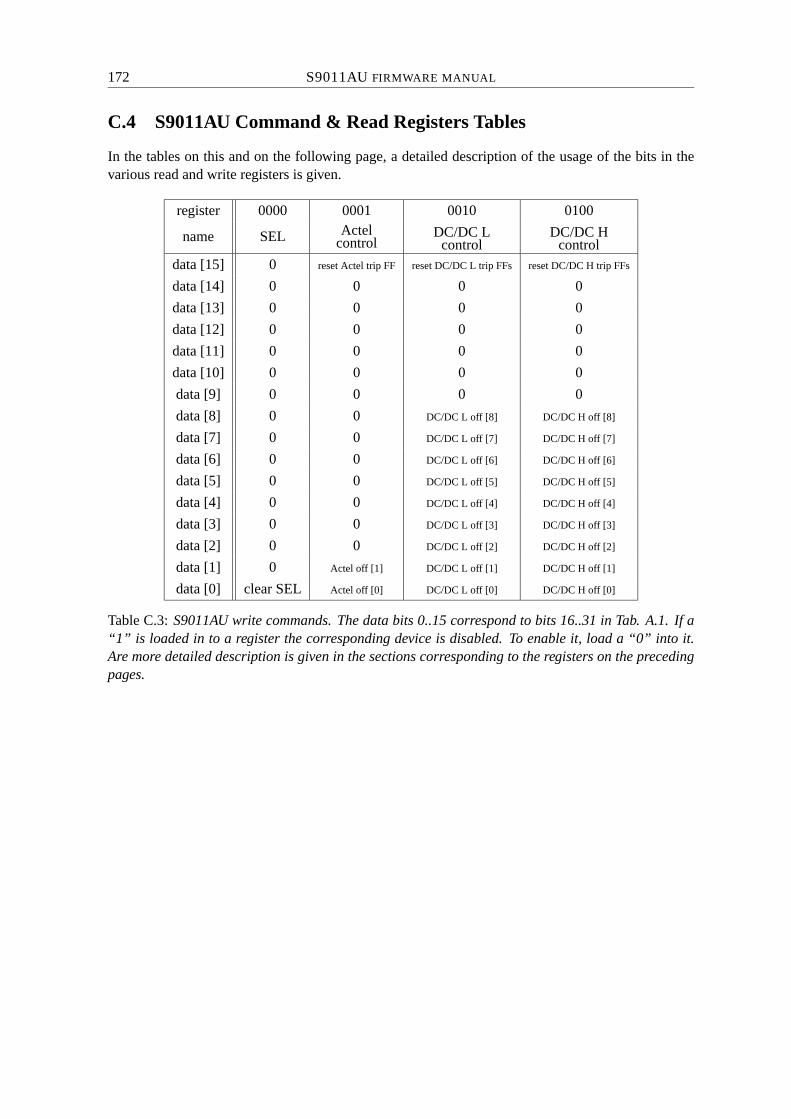
172 S9011AU FIRMWARE MANUAL
C.4 S9011AU Command & Read Registers Tables
In the tables on this and on the following page, a detailed description of the usage of the bits in thevarious read and write registers is given.
register 0000 0001 0010 0100
name SEL Actelcontrol
DC/DC Lcontrol
DC/DC Hcontrol
data [15] 0 reset Actel trip FF reset DC/DC L trip FFs reset DC/DC H trip FFs
data [14] 0 0 0 0
data [13] 0 0 0 0
data [12] 0 0 0 0
data [11] 0 0 0 0
data [10] 0 0 0 0
data [9] 0 0 0 0
data [8] 0 0 DC/DC L off [8] DC/DC H off [8]
data [7] 0 0 DC/DC L off [7] DC/DC H off [7]
data [6] 0 0 DC/DC L off [6] DC/DC H off [6]
data [5] 0 0 DC/DC L off [5] DC/DC H off [5]
data [4] 0 0 DC/DC L off [4] DC/DC H off [4]
data [3] 0 0 DC/DC L off [3] DC/DC H off [3]
data [2] 0 0 DC/DC L off [2] DC/DC H off [2]
data [1] 0 Actel off [1] DC/DC L off [1] DC/DC H off [1]
data [0] clear SEL Actel off [0] DC/DC L off [0] DC/DC H off [0]
Table C.3: S9011AU write commands. The data bits 0..15 correspond to bits 16..31 in Tab. A.1. If a“1” is loaded in to a register the corresponding device is disabled. To enable it, load a “0” into it.Are more detailed description is given in the sections corresponding to the registers on the precedingpages.

C.4 S9011AU COMMAND & READ REGISTERS TABLES 173
regi
ster
0000
0001
0010
0011
0100
0101
nam
eSE
LA
ctel
DC
/DC
Lla
stco
mm
and
DC
/DC
Ltr
ipFl
ipFl
ops
DC
/DC
Hla
stco
mm
and
DC
/DC
Htr
ipFl
ipFl
ops
data
[15]
00
00
00
data
[14]
00
00
00
data
[13]
00
00
00
data
[12]
00
00
00
data
[11]
00
00
00
data
[10]
00
00
00
data
[9]
00
00
00
data
[8]
0A
ctel
trip
FFD
C/D
CL
last
com
man
d[8
]D
C/D
CL
trip
FF[8
]D
C/D
CH
last
com
man
d[8
]D
C/D
CH
trip
FF[8
]
data
[7]
00
DC
/DC
Lla
stco
mm
and
[7]
DC
/DC
Ltr
ipFF
[7]
DC
/DC
Hla
stco
mm
and
[7]
DC
/DC
Htr
ipFF
[7]
data
[6]
00
DC
/DC
Lla
stco
mm
and
[6]
DC
/DC
Ltr
ipFF
[6]
DC
/DC
Hla
stco
mm
and
[6]
DC
/DC
Htr
ipFF
[6]
data
[5]
00
DC
/DC
Lla
stco
mm
and
[5]
DC
/DC
Ltr
ipFF
[5]
DC
/DC
Hla
stco
mm
and
[5]
DC
/DC
Htr
ipFF
[5]
data
[4]
0A
ctel
stat
usD
C/D
CL
last
com
man
d[4
]D
C/D
CL
trip
FF[4
]D
C/D
CH
last
com
man
d[4
]D
C/D
CH
trip
FF[4
]
data
[3]
00
DC
/DC
Lla
stco
mm
and
[3]
DC
/DC
Ltr
ipFF
[3]
DC
/DC
Hla
stco
mm
and
[3]
DC
/DC
Htr
ipFF
[3]
data
[2]
00
DC
/DC
Lla
stco
mm
and
[2]
DC
/DC
Ltr
ipFF
[2]
DC
/DC
Hla
stco
mm
and
[2]
DC
/DC
Htr
ipFF
[2]
data
[1]
0A
ctel
last
com
man
d[1
]D
C/D
CL
last
com
man
d[1
]D
C/D
CL
trip
FF[1
]D
C/D
CH
last
com
man
d[1
]D
C/D
CH
trip
FF[1
]
data
[0]
SEL
Act
ella
stco
mm
and
[0]
DC
/DC
Lla
stco
mm
and
[0]
DC
/DC
Ltr
ipFF
[0]
DC
/DC
Hla
stco
mm
and
[0]
DC
/DC
Htr
ipFF
[0]
Tabl
eC
.4:
S901
1AU
read
com
man
ds:
last
com
man
ds(=
desi
red
valu
e)&
trip
flip-
flops
.A
“1”
corr
espo
nds
to“
off”
or“
erro
r”,w
hile
a“
0”co
rres
pond
sto
“on
”or
“ok
ay”
.M
ore
deta
ils
onth
edi
ffere
ntre
gist
ers
can
befo
und
inth
eco
rres
pond
ing
sect
ions
onth
epr
eced
ing
page
s.

Appendix D
Analysis Algorithms for SUCIMA
D.1 LabView
In the following the most important analysis algorithms used in the SUCIMA software will be intro-duced. One set of algorithms is used for the initial calculation of the pedestal, the noise and the badpixel mask. A second set is used for the computation of the values updated after each frame. Themain focus of this section will be set on the algorithms used in the cluster search.
D.1.1 Pedestals
The pedestals represent the leakage current of the pixel of the CMOS sensor. In order to achieve acorrect calibration of the signal, the leakage current must be subtracted from the raw data before it isprocessed further.
• initial pedestals:For the initial calculation of the pedestals nmax frames are acquired from the sensor. From theseframes the average is computed separately for each pixel.
Pedestalsxy =1
nmax
n=nmax
∑n=1
Framenxy (D.1)
• updated pedestals:For the updated pedestals a different algorithm is used. This is required, as the memory usageto keep the nmax last frames ready for recalculation would be too high, especially for the largescale sensors like MIMOSA-V. Thus an algorithm was chosen, that follows the trends slower,but uses almost no memory and is faster as well. To keep rounding errors within the tolerance,the computation is done with double precision.
Pedestalsnew =Pedestalsold ∗ (nmax −1)+(Frame−Clusters)
nmax(D.2)
D.1.2 Noise
The noise is defined as the fluctuations of the pedestals around their mean value. The noise matrix isused for two purposes. The first is the computing of the bad pixel mask, the second is in the clustersearch.
• initial noise:The initial noise computation is divided into two parts. In the first part the noise is simply
175

176 ANALYSIS ALGORITHMS FOR SUCIMA
calculated as the standard deviation of the fluctuation of the nmax frames around the pedestals.
Noisexy =
√1
nmax
n=nmax
∑n=1
(Framen
xy −Pedestals)2
(D.3)
Between the first and the second iteration the BPM = Bad Pixel Mask has to be calculated, asin the second iteration the pixels above the noise threshold are masked. A further difference tothe first iteration is the application of a common mode correction.
Noise2xy =BPM× 1
nmax
n=nmax
∑n=1
[(Framen
xy −Pedestals)
− 1ymax
y=ymax
∑y=1
(Framen
xy −Pedestals)]2
(D.4)
• updated noise:For the evaluation of the updated noise matrix, like for the pedestals, a less memory intense andfaster algorithm was chosen. The deviation of the current frame, after removing the commonmode noise and the hit clusters, from the new pedestals is added quadratically to the old noise.Again these calculations are done using double precision to minimise the errors due to rounding.
Noise2new =
1nmax
×
Noise2old ∗ (nmax −1)
+[(Frame−Pedestals−Common Mode−Clusters)×BPM]2 (D.5)
D.1.3 Common Mode Noise
The common mode is a fluctuation in the signal from the sensor that is common, thus the name, tomany or even all pixels. As a large common mode variation across the sensor was observed, thealgorithm calculates the common mode on a per row basis.
If pixels containing “real” signals would be included in the calculation of the common mode, thevalue for the common mode noise would be too high. Thus pixels with a value 3 times higher than thenoise are excluded from the common mode calculation.
To correct for the common mode noise, the average of the pixels of a row with values within this3σ corridor is computed and then subtracted from all pixels in this row. This is done for all rows inthe data frame.
CMxy =1n
ymax
∑y=1
[(Framexy −Pedestalsxy)y
!< 3 ·Noisexy
](D.6)
With n = number of pixels in the row with values < 3 times the noise.
D.1.4 Bad Pixel Masking
For the computation of the initial and the updated bad pixel mask the same algorithm is used, as it isa simple and fast calculation, that simply compares the noise of a pixel to two thresholds. The lowerthreshold is 0, a pixel with no noise at all is regarded as “dead”. The upper threshold is a cut on pixelstoo noisy. This is required as such pixels would spoil the energy resolution of the system.
BPMxy =
1 0 < Noisexy ≤ Threshold
0 0 ≥ Noisexy ∨ Noisexy > Threshold(D.7)

D.2 MATHEMATICA 177
D.1.5 Cluster Search
The algorithm for the cluster search is divided into two parts. In the first segment the so-called seedpixel is searched and compared to a threshold, in the second a sub-matrix around the seed pixel iscompared to the corresponding threshold. Once a cluster has been identified and passed both criteria,it is masked and the algorithm loops once more on the data frame.
• seed pixel:To find the seed pixel the array is searched for the pixel with the highest signal to noise ratio.If the pixel found has a ratio larger than the specified threshold value, the algorithm goes to thenext step, the cluster analysis. If the pixel is below the threshold, there are no more seed pixelsin this frame and the cluster search on the current frame is terminated.
Dataxy/Noisexy?> 1st cut (D.8)
• cluster:If the seed pixel has passed the first criterium, the algorithm checks if the cluster around theseed pixel passes also the second criterium, the cut on the signal to noise of the sub-matrixaround the seed pixel.
In this comparison the signal is defined as the sum of the value of all the pixels in the sub-matrix,while the noise is defined as the Root-Mean-Square (RMS) of the noise of the individual pixelsin the sub-matrix.
The size of the sub-matrix around the seed pixel can be set to 3×3, 5×5 and so on.
x,y=max
∑x,y=1
Dataxy?> 2nd cut ×
√√√√x,y=max
∑x,y=1
Noise2xy (D.9)
• hit limit:As a too high number of hits in one frame could lead to an overlapping of the individual hitsand thus a wrong value for the height of the cluster signal, a limit can be set on the maximumnumber of clusters per frame. If more clusters are found in the frame, the current frame isskipped, its results omitted and the next frame is acquired and processed. This also removesissues with “hot” frames.
D.2 Mathematica
The analysis of the data taken during the radiation hardness studies on the SUCCESSOR-I chip wasdone using a Mathematica 5 script written by Michael Deveaux [Dev03]. It uses basically the samealgorithms as the LabView software, but there are some small differences.
• Leakage Current I: In principle the leakage current of the pixels can be derived from thepedestals, but for non-irradiated chips and high read out frequencies the values can be in theorder of the resolution of the ADC.
To increase the integration time by a factor of 6, and to check the time constant of the discharg-ing, this method uses 8 consecutive frames between two resets. The first frame after the resetis discarded to allow for settling effects, from the other 7 the difference between frame #2 andframe #n is calculated.
CDSi = Framen −Frame2 with n ∈ 2..8 (D.10)

178 ANALYSIS ALGORITHMS FOR SUCIMA
One measurement run consists of 500 such 8-frame sets. The first 40 of these sets were not usedfor the analysis, as the chip has a rather high common mode noise after starting the clock. Fromthe other sets the mean value is computed for each CDS sample separately for each pixel.
Mi =1
rmax
rmax
∑r=rmin
CDSir with r ∈ 40..500 (D.11)
To these 6 data points of each of the pixels a linear fit is made, in which the slope S correspondsto the leakage current. These are then averaged over all pixels. The mean value is used for theleakage current and the deviation for the error, as the pixel to pixel spread is much larger thanthe error of the linear fit.
LC = B+S · i (D.12)
Ileak =(S±σS
) · ν ·qA ·N (D.13)
With ν = read out frequency, q = e− = 1.6× 10⁻¹⁹C, N = number of pixels (including markerpixels) = 2112 and A = calibration of the ADC.
The calibration of the ADC is derived from the position of the small peak in the 55Fe spectrumas this corresponds to a well known amount of charge, that is generated in the sensor.
A =small peak position [ADC]
Eγ/Egeneration(D.14)
55Fe has two characteristic lines, one at 5.89keV with a branching ratio of 24.4%, the otherat 6.49keV (3.40%). For the calibration of the devices the 5.89keV gammas were used. Theenergy required to generate a electron-hole pair in silicon is 3.6eV .
• Leakage Current II: After acquiring nmax = 10000 CDS frames without a source on the sensor,the average of these is computed for each pixel.
Mxy =1
nmax
nmax
∑n=1
Framexy (D.15)
To the distribution of these values Mxy a Gaussian is fit. The following equation is used tocalculate the leakage current in Ampere from the value of the centre of the Gaussian.
Ileak = (C) · ν ·qA ·N (D.16)
With C = Centre of the Gaussian, ν = read out frequency, q = e− = 1.6×10⁻¹⁹C, N = numberof pixels (including marker pixels) = 2112 and A = calibration of the ADC, see above.
The error of the value of the leakage current is given by the width of the Gaussian, as the erroris dominated by the pixel to pixel variation and not by the fluctuation of the pixel value itself.
I = I± t · σgauss
n(D.17)
Where I is the mean value for the measurement, σgauss the width of the distribution, n thenumber of pixels in a sub-matrix (= 32×32 = 1024) and t the value of the Student function fora given n and given confidence level. During the evaluation of the measurements a conservativeapproach was used and for a confidence level of 95.8% the value of the student function wasassumed to be t = 2.

D.2 MATHEMATICA 179
• 55Fe -spectra: Like in the LabView VI the algorithm searching for clusters in the data is seg-mented into different parts. The first part calculates the initial pedestals and noise, the secondthe common mode noise, the third the pedestals and noise corrected for common mode, thefourth part looks for hits and the fifth part updates the pedestals and noise. In the final part thehistograms for the seed pixel and the various cluster sizes are updated.
– Initial Pedestals & Noise: At the start of the algorithm 20 samples with 5 CDS frames eachare read. From each sample the maximum value of each pixel is removed. This is done toremove any hits from the data, as they would lead to wrong values for the pedestals andthe noise. After this the data is combined into one array.From this array one computes the pedestals:
Pedestalsinitxy =
1nmax
nmax
∑n=1
Dataxy (D.18)
and the noise:
Noiseinitxy =
√1
nmax
nmax
∑n=1
(Dataxy −Pedestalsinit
xy
)2(D.19)
with nmax = number of frames in the combined array Dataxy.
– Common Mode Noise: In the common mode noise correction disturbances affecting manypixels in a frame are compensated. In a first step the pedestals are subtracted from the CDSframe.
Fxy = Framexy −Pedestalsinitxy (D.20)
As hits in the data would lead to wrong values for the common mode they have to beomitted from the further calculation. This is done by applying a cut on the signal to noiseratio (SNR).
Kxy =
Fxy if Fxy < k ·Noiseinit
xy
0 if Fxy ≥ k ·Noiseinitxy
(D.21)
In this case k was set to 5.If the algorithm finds too many pixels with signals above the threshold, the frame is notprocessed further, as there is a high probability that the data taking was disturbed.The common mode CMy is then calculated on a per row basis as the average of the valuesKxy in this row and subtracted from all pixels in this row.
Dxy = Fxy −CMinity with CMinit
y =1
ymax
ymax
∑y=1
Kxy (D.22)
– Pedestals & Noise: To increase the precision of the pedestals and the noise both are re-iterated after applying the common mode correction to the data set.
Dxy = Framexy −CMinity −Pedestalsinit
xy (D.23)
Frames with a too high common mode are excluded from the further calculation. If thereare too many frames failing this criteria, the computation is aborted.To this data set again a threshold (k = 5) on the SNR is applied to remove any possiblehits, that might have been masked by a high common mode, from the calculation of thepedestals and the noise.
Kxy =
Dxy Dxy < k ·Noiseinit
xy
0 Dxy ≥ k ·Noiseinitxy
(D.24)
180 ANALYSIS ALGORITHMS FOR SUCIMA
The “new” pedestals and noise can be calculated as:
Pedestalsxy = Pedestalsinitxy +Pxy with Pxy =
1nmax
nmax
∑n=1
Dxy (D.25)
Noisexy =
√1
nmax
nmax
∑n=1
(Dxy −Pxy)2 (D.26)
With nmax = number of frames taken into account for the calculation.
– Cluster Search: When looking for hits in the data, one has first to remove the pedestalsand the common mode noise from the acquired data.
Sxy = Framexy −Pedestalsxy −CMy (D.27)
where CMy is the common mode calculated using Pedestalsxy and Noisexy.For possible seed pixels it is required that
Sxy/Noisexy!> cseed with cseed = 5 (D.28)
Additionally, the seed pixel, the pixel with the highest SNR in the cluster, has to be 2 ormore pixels away from the edge of the chip, as the cluster size is 5× 5 pixels, with theseed pixel at the centre, and all clusters have to be complete for further processing.In case of overlapping clusters only the one with the higher SNR is used in the furthercomputation, the weaker one is masked. This is done by sorting the clusters found accord-ing to their SNR and starting the further processing from the cluster with the highest SNR,always keeping the addresses of the previous hits in memory and checking for possibleoverlays.To the remaining clusters a second cut is applied. The summed signal of the 3×3 matrixaround the seed pixel has to be 3 times larger than the Root-Mean-Square (RMS) noise ofthe matrix.
1
∑i, j=−1
Sx+i,y+i!> ccluster ·
√√√√ 1
∑i, j=−1
(Noisex+i,y+i)2 (D.29)
with x,y= coordinates of the seed pixel and ccluster = 3.
– Updated Pedestals & Noise: As the pedestals and the noise of the sensor are not constantover time, both, pedestals and noise, are updated after each frame.In the first iteration two intermediate arrays are filled
1Ixy =
Pedestalsxy if x,y inside a cluster
Framexy −CMy else(D.30)
2Ixy =
Noisexy if x,y inside a cluster
Framexy −Pedestalsxy −CMy else(D.31)
Using these arrays, the updated pedestals and noise can be calculated.
Pedestalsnewxy =
1n
[(n−1) ·Pedestalsxy +1 Ixy
](D.32)
Noisenewxy =
√1n
[(n−1) · (Noisexy)2 +(2Ixy)2] (D.33)
where n is the number of frames that should be included in the pedestal and noise calcu-lation.

D.2 MATHEMATICA 181
– Histograms: At the end of the analysis the following histograms presenting the data arebuilt:
* Seed Pixel Spectrum: For each cluster the value of the pixel with the highest SNR isentered into this histogram. This is done for all frames from the run.
* Cluster Spectra: To build the cluster spectra, the values of the pixels in one cluster arefirst sorted according to their height, and then a certain number of pixels is summed.These sums are calculated for a number of pixels included from 2 to 25 and thenentered into the corresponding histograms. This is done for all clusters passing thetwo criteria from all frames. The histograms used for the radiation hardness studiesare the 9 and the 25 pixel histograms, which correspond, in most cases, to a 3×3 anda 5×5 matrix around the seed pixel.
* Pedestal Distribution: Two histograms are built from the pedestal data. One from theinitial computation and one from the last updated pedestals. This allows to check fortime dependent phenomena or temperature drifts of the sensor.
* Noise Distribution: Also for the noise two histograms are generated. Again, one fromthe initial calculation and one from the last updated noise. There, the same motivationas for the pedestals comes into play.
As the Mathematica script has to be run in the interpreter mode of Mathematica and cannot becompiled, due to the different commands in the two modes, the analysis has serious issues with per-formance and memory usage. A port of the script to ROOT was written by Gotz Gaycken, but thecode was not verified before the end of this thesis and thus not used for the data presented here.

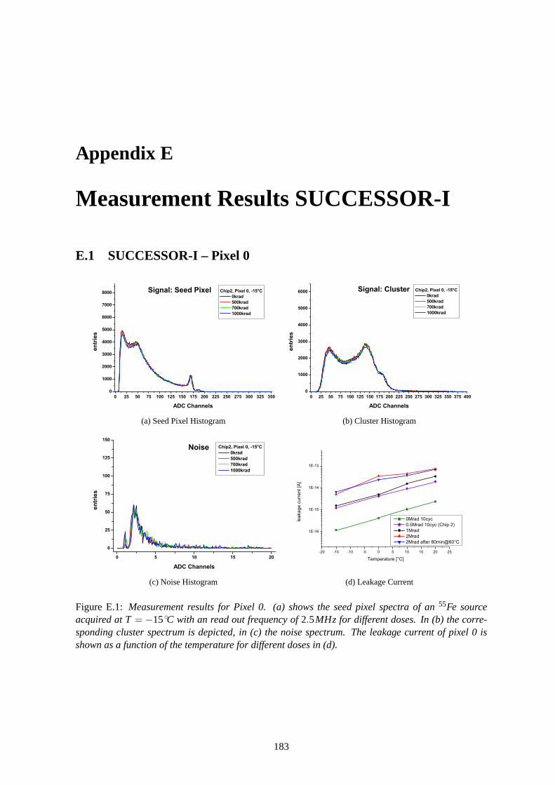
Appendix E
Measurement Results SUCCESSOR-I
E.1 SUCCESSOR-I – Pixel 0
(a) Seed Pixel Histogram (b) Cluster Histogram
(c) Noise Histogram (d) Leakage Current
Figure E.1: Measurement results for Pixel 0. (a) shows the seed pixel spectra of an 55Fe sourceacquired at T = −15 C with an read out frequency of 2.5MHz for different doses. In (b) the corre-sponding cluster spectrum is depicted, in (c) the noise spectrum. The leakage current of pixel 0 isshown as a function of the temperature for different doses in (d).
183
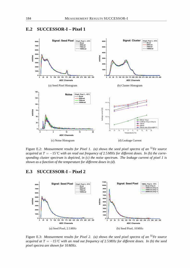
184 MEASUREMENT RESULTS SUCCESSOR-I
E.2 SUCCESSOR-I – Pixel 1
(a) Seed Pixel Histogram (b) Cluster Histogram
(c) Noise Histogram (d) Leakage Current
Figure E.2: Measurement results for Pixel 1. (a) shows the seed pixel spectra of an 55Fe sourceacquired at T = −15 C with an read out frequency of 2.5MHz for different doses. In (b) the corre-sponding cluster spectrum is depicted, in (c) the noise spectrum. The leakage current of pixel 1 isshown as a function of the temperature for different doses in (d).
E.3 SUCCESSOR-I – Pixel 2
(a) Seed Pixel, 2.5MHz (b) Seed Pixel, 10MHz
Figure E.3: Measurement results for Pixel 2. (a) shows the seed pixel spectra of an 55Fe sourceacquired at T = −15 C with an read out frequency of 2.5MHz for different doses. In (b) the seedpixel spectra are shown for 10MHz.
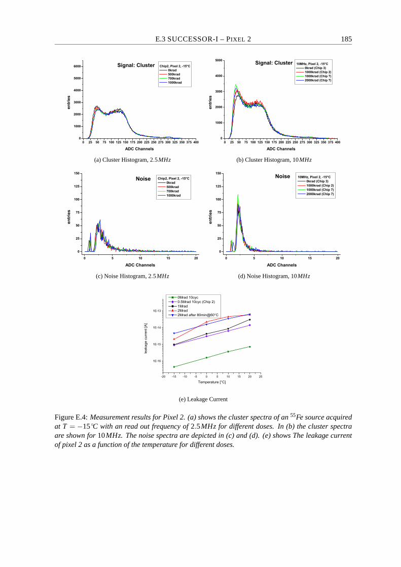
E.3 SUCCESSOR-I – PIXEL 2 185
(a) Cluster Histogram, 2.5MHz (b) Cluster Histogram, 10MHz
(c) Noise Histogram, 2.5MHz (d) Noise Histogram, 10MHz
(e) Leakage Current
Figure E.4: Measurement results for Pixel 2. (a) shows the cluster spectra of an 55Fe source acquiredat T = −15 C with an read out frequency of 2.5MHz for different doses. In (b) the cluster spectraare shown for 10MHz. The noise spectra are depicted in (c) and (d). (e) shows The leakage currentof pixel 2 as a function of the temperature for different doses.
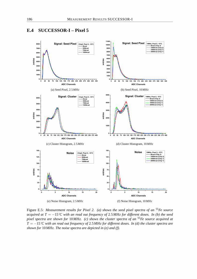
186 MEASUREMENT RESULTS SUCCESSOR-I
E.4 SUCCESSOR-I – Pixel 5
(a) Seed Pixel, 2.5MHz (b) Seed Pixel, 10MHz
(c) Cluster Histogram, 2.5MHz (d) Cluster Histogram, 10MHz
(e) Noise Histogram, 2.5MHz (f) Noise Histogram, 10MHz
Figure E.5: Measurement results for Pixel 2. (a) shows the seed pixel spectra of an 55Fe sourceacquired at T = −15 C with an read out frequency of 2.5MHz for different doses. In (b) the seedpixel spectra are shown for 10MHz. (c) shows the cluster spectra of an 55Fe source acquired atT = −15 C with an read out frequency of 2.5MHz for different doses. In (d) the cluster spectra areshown for 10MHz. The noise spectra are depicted in (e) and (f).
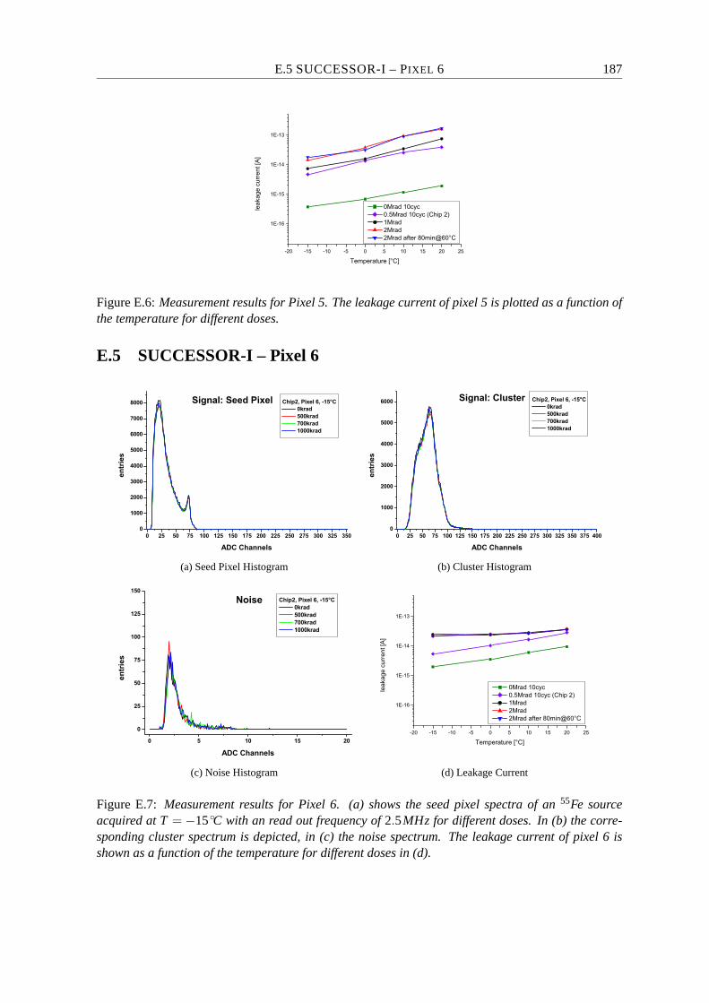
E.5 SUCCESSOR-I – PIXEL 6 187
Figure E.6: Measurement results for Pixel 5. The leakage current of pixel 5 is plotted as a function ofthe temperature for different doses.
E.5 SUCCESSOR-I – Pixel 6
(a) Seed Pixel Histogram (b) Cluster Histogram
(c) Noise Histogram (d) Leakage Current
Figure E.7: Measurement results for Pixel 6. (a) shows the seed pixel spectra of an 55Fe sourceacquired at T = −15 C with an read out frequency of 2.5MHz for different doses. In (b) the corre-sponding cluster spectrum is depicted, in (c) the noise spectrum. The leakage current of pixel 6 isshown as a function of the temperature for different doses in (d).
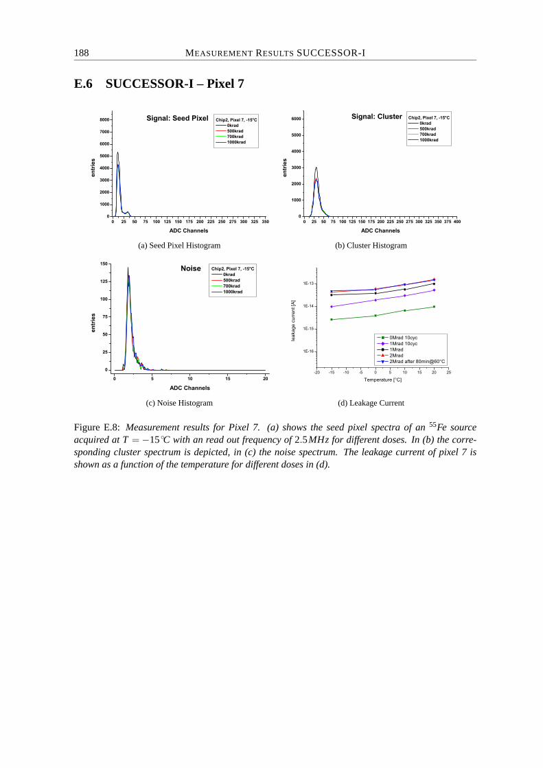
188 MEASUREMENT RESULTS SUCCESSOR-I
E.6 SUCCESSOR-I – Pixel 7
(a) Seed Pixel Histogram (b) Cluster Histogram
(c) Noise Histogram (d) Leakage Current
Figure E.8: Measurement results for Pixel 7. (a) shows the seed pixel spectra of an 55Fe sourceacquired at T = −15 C with an read out frequency of 2.5MHz for different doses. In (b) the corre-sponding cluster spectrum is depicted, in (c) the noise spectrum. The leakage current of pixel 7 isshown as a function of the temperature for different doses in (d).

Acknowledgements
The broad spectrum of this thesis, covering different technologies and methods, would not have beenpossible without the support of my supervisors and my colleagues and the plentiful discussions withthem. At this time I would like to thank all of them.I would like to thank Prof. Wim de Boer for the great possibility he offered me with this PhD thesis,his scientific input and his support for my ideas together with his complete trust in my capabilities.Prof. Thomas Muller honoured me with accepting the co-reference and supporting my work.For the fruitful discussions on many topics I would like to thank the colleagues in my group. Inalphabetical order: Johannes Bol, Alexander Dierlamm, Alexander Furgeri, Eugene Grigoriev, Flo-rian Hauler, Michael Koppenhofer & Mike Schmanau. They also contributed to the preparation andimplementation of many measurements.For her help with the construction of electronics I would like to thank Pia Steck. I am very gratefulto Tobias Barvich, without his help many ideas for mechanics would never have been made real. Healso acted as an interface to our great mechanical workshop.A very special thanks goes to our administrative group: Diana Fellner-Thedens, Sven Fuchs andEdeltraud Haas. Without their support many things would not have been possible.For his help with the day to day IT issues, and some more exotic ones, I would like to thank Hans-Jurgen Simonis.This is also the moment to thank all the people, who were proof-reading this thesis: Jutta Bol, FrankHartmann, Stephan Heising, Bernhard Ledermann, Jens Rehn, Marcel Stanitzki and Julia Walther.Last but not least I’m indebted to my girlfriend Julia, my friends and of course my family for theirgreat support during the last years.
This PhD thesis was supported by the European Community within the V (Growth) Framework.SUCIMA project – Contract no. G1RD-CT-2001-00561.
All trademarks and registered trademarks are the property of their respective owners.
189

List of Figures
1.1 The International Space Station . . . . . . . . . . . . . . . . . . . . . . . . . . . . 31.2 The Bess Experiment . . . . . . . . . . . . . . . . . . . . . . . . . . . . . . . . . . 41.3 The PAMELA Experiment . . . . . . . . . . . . . . . . . . . . . . . . . . . . . . . . 51.4 The AMS01 Detector on-board Discovery . . . . . . . . . . . . . . . . . . . . . . . 61.5 The AMS01 Detector . . . . . . . . . . . . . . . . . . . . . . . . . . . . . . . . . . 61.6 The AMS02 Detector . . . . . . . . . . . . . . . . . . . . . . . . . . . . . . . . . . 71.7 The Transition Radiation Detector . . . . . . . . . . . . . . . . . . . . . . . . . . . 81.8 A Strawtube Module . . . . . . . . . . . . . . . . . . . . . . . . . . . . . . . . . . 81.9 Cross-Section of a Strawtube Wall & a TRD Layer . . . . . . . . . . . . . . . . . . 91.10 TRD Gas System . . . . . . . . . . . . . . . . . . . . . . . . . . . . . . . . . . . . 91.11 Performance of the TRD . . . . . . . . . . . . . . . . . . . . . . . . . . . . . . . . 101.12 The Time-of-Flight Detector . . . . . . . . . . . . . . . . . . . . . . . . . . . . . . 111.13 Performance of the TOF . . . . . . . . . . . . . . . . . . . . . . . . . . . . . . . . 111.14 The AMS02 Tracker . . . . . . . . . . . . . . . . . . . . . . . . . . . . . . . . . . . 121.15 Tracker Plane & Ladder . . . . . . . . . . . . . . . . . . . . . . . . . . . . . . . . 131.16 Tracker Thermal Control System . . . . . . . . . . . . . . . . . . . . . . . . . . . . 131.17 The Superconducting Magnet of AMS02 . . . . . . . . . . . . . . . . . . . . . . . . 141.18 Spatial Resolution of the Silicon Tracker . . . . . . . . . . . . . . . . . . . . . . . . 151.19 dE/dx Measurement using the Silicon Tracker . . . . . . . . . . . . . . . . . . . . . 161.20 The Anti-Coincidence Counter . . . . . . . . . . . . . . . . . . . . . . . . . . . . . 161.21 Performance of the ACC . . . . . . . . . . . . . . . . . . . . . . . . . . . . . . . . 171.22 The AMS02 RICH . . . . . . . . . . . . . . . . . . . . . . . . . . . . . . . . . . . . 171.23 Performance of the RICH . . . . . . . . . . . . . . . . . . . . . . . . . . . . . . . . 181.24 Spectrum - Tracker + RICH . . . . . . . . . . . . . . . . . . . . . . . . . . . . . . 181.25 The Electromagnetic Calorimeter of AMS02 . . . . . . . . . . . . . . . . . . . . . . 191.26 Performance of the ECAL . . . . . . . . . . . . . . . . . . . . . . . . . . . . . . . . 201.27 The Star Tracker . . . . . . . . . . . . . . . . . . . . . . . . . . . . . . . . . . . . 201.28 Beta Angle of the ISS . . . . . . . . . . . . . . . . . . . . . . . . . . . . . . . . . . 221.29 The AMS02 Particle Signatures . . . . . . . . . . . . . . . . . . . . . . . . . . . . . 231.30 Element Abundances in GCR & Solar System . . . . . . . . . . . . . . . . . . . . . 241.31 Energy Spectrum of Cosmic Rays . . . . . . . . . . . . . . . . . . . . . . . . . . . . 251.32 Anti-Proton Spectrum . . . . . . . . . . . . . . . . . . . . . . . . . . . . . . . . . . 301.33 The Positron Fraction . . . . . . . . . . . . . . . . . . . . . . . . . . . . . . . . . . 311.34 Anti-Helium Limits . . . . . . . . . . . . . . . . . . . . . . . . . . . . . . . . . . . 321.35 Rotation Curve NGC 1560 . . . . . . . . . . . . . . . . . . . . . . . . . . . . . . . 351.36 Diffuse Gamma Ray Sepctra . . . . . . . . . . . . . . . . . . . . . . . . . . . . . . 361.37 Halo Profile . . . . . . . . . . . . . . . . . . . . . . . . . . . . . . . . . . . . . . . 361.38 The Transition Radiation Yield . . . . . . . . . . . . . . . . . . . . . . . . . . . . . 38
2.1 The Radiators . . . . . . . . . . . . . . . . . . . . . . . . . . . . . . . . . . . . . . 39
191

192 LIST OF FIGURES
2.2 AMS02 Electronics Overview . . . . . . . . . . . . . . . . . . . . . . . . . . . . . . 412.3 DAQ Structure of AMS02 . . . . . . . . . . . . . . . . . . . . . . . . . . . . . . . . 412.4 Slow-Control Structure of AMS02 . . . . . . . . . . . . . . . . . . . . . . . . . . . 432.5 AMS02 Trigger Scheme . . . . . . . . . . . . . . . . . . . . . . . . . . . . . . . . . 442.6 TRD Read Out Electronics Overview . . . . . . . . . . . . . . . . . . . . . . . . . . 452.7 Data Scheme TRD . . . . . . . . . . . . . . . . . . . . . . . . . . . . . . . . . . . . 462.8 Power Scheme TRD . . . . . . . . . . . . . . . . . . . . . . . . . . . . . . . . . . . 462.9 The U-Crate . . . . . . . . . . . . . . . . . . . . . . . . . . . . . . . . . . . . . . . 472.10 The U-Backplane . . . . . . . . . . . . . . . . . . . . . . . . . . . . . . . . . . . . 482.11 JINF . . . . . . . . . . . . . . . . . . . . . . . . . . . . . . . . . . . . . . . . . . . 492.12 CDDC . . . . . . . . . . . . . . . . . . . . . . . . . . . . . . . . . . . . . . . . . . 492.13 UDR2 . . . . . . . . . . . . . . . . . . . . . . . . . . . . . . . . . . . . . . . . . . 502.14 Common Digital Part . . . . . . . . . . . . . . . . . . . . . . . . . . . . . . . . . . 512.15 UFE . . . . . . . . . . . . . . . . . . . . . . . . . . . . . . . . . . . . . . . . . . . 522.16 UTE & UFE . . . . . . . . . . . . . . . . . . . . . . . . . . . . . . . . . . . . . . . 522.17 USCM . . . . . . . . . . . . . . . . . . . . . . . . . . . . . . . . . . . . . . . . . . 532.18 UHVG . . . . . . . . . . . . . . . . . . . . . . . . . . . . . . . . . . . . . . . . . . 542.19 UHVG Calibration . . . . . . . . . . . . . . . . . . . . . . . . . . . . . . . . . . . 542.20 UPSFE . . . . . . . . . . . . . . . . . . . . . . . . . . . . . . . . . . . . . . . . . 552.21 Multi-point LVDS . . . . . . . . . . . . . . . . . . . . . . . . . . . . . . . . . . . . 562.22 The UPD . . . . . . . . . . . . . . . . . . . . . . . . . . . . . . . . . . . . . . . . 572.23 S9011AU . . . . . . . . . . . . . . . . . . . . . . . . . . . . . . . . . . . . . . . . 582.24 S9011B . . . . . . . . . . . . . . . . . . . . . . . . . . . . . . . . . . . . . . . . . 592.25 DC/DC Converter . . . . . . . . . . . . . . . . . . . . . . . . . . . . . . . . . . . . 602.26 Apex FPGA / Actel Anti-Fuse . . . . . . . . . . . . . . . . . . . . . . . . . . . . . . 632.27 FPGA Socket . . . . . . . . . . . . . . . . . . . . . . . . . . . . . . . . . . . . . . 642.28 D-FlipFlop with Asynchronous Reset . . . . . . . . . . . . . . . . . . . . . . . . . . 652.29 UDR Firmware Architecture . . . . . . . . . . . . . . . . . . . . . . . . . . . . . . 672.30 S9007 & Table Top Setup . . . . . . . . . . . . . . . . . . . . . . . . . . . . . . . . 682.31 UDR Sequence - Read Out . . . . . . . . . . . . . . . . . . . . . . . . . . . . . . . 692.32 UDR Sequence - Calibration . . . . . . . . . . . . . . . . . . . . . . . . . . . . . . 692.33 Sequencer: Delay scan . . . . . . . . . . . . . . . . . . . . . . . . . . . . . . . . . 712.34 Sequencer: Linearity scan . . . . . . . . . . . . . . . . . . . . . . . . . . . . . . . 712.35 Sequencer: Sr90 . . . . . . . . . . . . . . . . . . . . . . . . . . . . . . . . . . . . . 722.36 LeCroy Line Oscillations . . . . . . . . . . . . . . . . . . . . . . . . . . . . . . . . 732.37 UPSFEv2 Firmware Scheme . . . . . . . . . . . . . . . . . . . . . . . . . . . . . . 732.38 S9011AU Firmware Scheme . . . . . . . . . . . . . . . . . . . . . . . . . . . . . . 742.39 Electronics Production Scheme . . . . . . . . . . . . . . . . . . . . . . . . . . . . . 762.40 Space Qualification - Board Level . . . . . . . . . . . . . . . . . . . . . . . . . . . 772.41 Space Qualification - Crate Level . . . . . . . . . . . . . . . . . . . . . . . . . . . . 782.42 EMI Test of TRD Prototype . . . . . . . . . . . . . . . . . . . . . . . . . . . . . . . 792.43 ESS Thermo Cycle . . . . . . . . . . . . . . . . . . . . . . . . . . . . . . . . . . . 792.44 Vibration Test . . . . . . . . . . . . . . . . . . . . . . . . . . . . . . . . . . . . . . 802.45 Thermo Vacuum Test . . . . . . . . . . . . . . . . . . . . . . . . . . . . . . . . . . 812.46 EM Test Backplane . . . . . . . . . . . . . . . . . . . . . . . . . . . . . . . . . . . 812.47 QM1 Test Backplane . . . . . . . . . . . . . . . . . . . . . . . . . . . . . . . . . . 822.48 UPSFEv2 Test Backplane . . . . . . . . . . . . . . . . . . . . . . . . . . . . . . . . 832.49 Linear Regulator Test Circuitry . . . . . . . . . . . . . . . . . . . . . . . . . . . . . 832.50 Software for UPSFE Test Backplane . . . . . . . . . . . . . . . . . . . . . . . . . . 842.51 UPSFEv2 Test Setup . . . . . . . . . . . . . . . . . . . . . . . . . . . . . . . . . . 842.52 Beam Test Setup 2002 . . . . . . . . . . . . . . . . . . . . . . . . . . . . . . . . . . 85

LIST OF FIGURES 193
2.53 Beam Test Data 2002 . . . . . . . . . . . . . . . . . . . . . . . . . . . . . . . . . . 862.54 TRD Beam Test October 2003 . . . . . . . . . . . . . . . . . . . . . . . . . . . . . 87
3.1 Energy Loss - Bethe Bloch . . . . . . . . . . . . . . . . . . . . . . . . . . . . . . . 903.2 Landau Distribution . . . . . . . . . . . . . . . . . . . . . . . . . . . . . . . . . . . 913.3 Attenuation Coefficient in Silicon . . . . . . . . . . . . . . . . . . . . . . . . . . . . 923.4 Silicon Microstrip Detector . . . . . . . . . . . . . . . . . . . . . . . . . . . . . . . 953.5 Hybrid Pixel . . . . . . . . . . . . . . . . . . . . . . . . . . . . . . . . . . . . . . . 963.6 Charge Coupled Device - CCD . . . . . . . . . . . . . . . . . . . . . . . . . . . . . 973.7 DEPFET . . . . . . . . . . . . . . . . . . . . . . . . . . . . . . . . . . . . . . . . 983.8 CMOS Pixel . . . . . . . . . . . . . . . . . . . . . . . . . . . . . . . . . . . . . . . 993.9 CMOS Pixel - 55Fe spectrum . . . . . . . . . . . . . . . . . . . . . . . . . . . . . . 1003.10 CMOS Pixel Read Out . . . . . . . . . . . . . . . . . . . . . . . . . . . . . . . . . 1003.11 Silicon On Insulator - SOI . . . . . . . . . . . . . . . . . . . . . . . . . . . . . . . 1023.12 Radiation Induced Displacement of Atoms . . . . . . . . . . . . . . . . . . . . . . . 1053.13 Si-SiO2 Interface Charge-Up . . . . . . . . . . . . . . . . . . . . . . . . . . . . . . 1063.14 Enclosed NMOS Transistor . . . . . . . . . . . . . . . . . . . . . . . . . . . . . . . 107
4.1 Balloon Catheter with Stent . . . . . . . . . . . . . . . . . . . . . . . . . . . . . . . 1104.2 Re-Stenosis . . . . . . . . . . . . . . . . . . . . . . . . . . . . . . . . . . . . . . . 1104.3 Comparison of Depth-Dose Curves . . . . . . . . . . . . . . . . . . . . . . . . . . . 1124.4 3D Irradiation . . . . . . . . . . . . . . . . . . . . . . . . . . . . . . . . . . . . . . 1124.5 The SLIM Principle . . . . . . . . . . . . . . . . . . . . . . . . . . . . . . . . . . . 1144.6 The SLIM Implementation . . . . . . . . . . . . . . . . . . . . . . . . . . . . . . . 1154.7 Silicon Micro-Strip Detector (SUCIMA) . . . . . . . . . . . . . . . . . . . . . . . . 1174.8 MIMOSA-V . . . . . . . . . . . . . . . . . . . . . . . . . . . . . . . . . . . . . . . 1184.9 MIMOSA-V Back-Thinning . . . . . . . . . . . . . . . . . . . . . . . . . . . . . . . 1194.10 MIMOSA-V HPD Setup . . . . . . . . . . . . . . . . . . . . . . . . . . . . . . . . . 1204.11 SUCCESSOR-I . . . . . . . . . . . . . . . . . . . . . . . . . . . . . . . . . . . . . 1204.12 SUCCESSOR-I Super-Pixel . . . . . . . . . . . . . . . . . . . . . . . . . . . . . . . 1214.13 SUCCESSOR-I Pixel Layout (0..1) . . . . . . . . . . . . . . . . . . . . . . . . . . . 1214.14 SUCCESSOR-1 Pixel Layout (2..7) . . . . . . . . . . . . . . . . . . . . . . . . . . . 1224.15 SUCCESSOR-II . . . . . . . . . . . . . . . . . . . . . . . . . . . . . . . . . . . . . 1234.16 SUCCESSOR-IV / MimoTERA . . . . . . . . . . . . . . . . . . . . . . . . . . . . . 1244.17 SOI Sensor . . . . . . . . . . . . . . . . . . . . . . . . . . . . . . . . . . . . . . . 1254.18 SUCIMA Imager DAQ PCB . . . . . . . . . . . . . . . . . . . . . . . . . . . . . . . 1264.19 SUCIMA USB DAQ System . . . . . . . . . . . . . . . . . . . . . . . . . . . . . . . 1274.20 SUCIMA Repeater . . . . . . . . . . . . . . . . . . . . . . . . . . . . . . . . . . . 1284.21 SUCIMA Pixel Hybrid . . . . . . . . . . . . . . . . . . . . . . . . . . . . . . . . . 1294.22 SUCIMA DAQ Software . . . . . . . . . . . . . . . . . . . . . . . . . . . . . . . . . 1304.23 Schematic Overview of the SUCIMA DAQ Software . . . . . . . . . . . . . . . . . . 131
5.1 The X-Ray Setup . . . . . . . . . . . . . . . . . . . . . . . . . . . . . . . . . . . . 1345.2 X-Ray Beam Spot . . . . . . . . . . . . . . . . . . . . . . . . . . . . . . . . . . . . 1345.3 The LEPSI Setup . . . . . . . . . . . . . . . . . . . . . . . . . . . . . . . . . . . . 1355.4 SUCCESSOR-I Carrier & Alignment . . . . . . . . . . . . . . . . . . . . . . . . . . 1365.5 Current Consumption of SUCCESSOR-I . . . . . . . . . . . . . . . . . . . . . . . . 1375.6 Inhomogeneous Pedestals of SUCCESSOR-I . . . . . . . . . . . . . . . . . . . . . . 1385.7 Infrared Picture of SUCCESSOR-I . . . . . . . . . . . . . . . . . . . . . . . . . . . 1385.8 Pixel 3 - Seed Pixel Histogram . . . . . . . . . . . . . . . . . . . . . . . . . . . . . 1415.9 Pixel 3 - Seed Pixel Histogram 10MHz . . . . . . . . . . . . . . . . . . . . . . . . . 141
194 LIST OF FIGURES
5.10 Pixel 3 - 3×3 Cluster Histogram . . . . . . . . . . . . . . . . . . . . . . . . . . . . 1425.11 Pixel 3 - 3×3 Cluster Histogram 10MHz . . . . . . . . . . . . . . . . . . . . . . . 1425.12 Pixel 3 - Noise Histogram . . . . . . . . . . . . . . . . . . . . . . . . . . . . . . . . 1435.13 Pixel 3 - Noise Histogram 10MHz . . . . . . . . . . . . . . . . . . . . . . . . . . . 1435.14 Pixel 3 - Leakage Current . . . . . . . . . . . . . . . . . . . . . . . . . . . . . . . . 1445.15 Pixel 4 - Seed Pixel Histogram . . . . . . . . . . . . . . . . . . . . . . . . . . . . . 1455.16 Pixel 4 - Seed Pixel Histogram 10MHz . . . . . . . . . . . . . . . . . . . . . . . . . 1455.17 Pixel 4 - 3×3 Cluster Histogram . . . . . . . . . . . . . . . . . . . . . . . . . . . . 1465.18 Pixel 4 - 3×3 Cluster Histogram 10MHz . . . . . . . . . . . . . . . . . . . . . . . 1465.19 Pixel 4 - Noise Histogram . . . . . . . . . . . . . . . . . . . . . . . . . . . . . . . . 1475.20 Pixel 4 - Noise Histogram 10MHz . . . . . . . . . . . . . . . . . . . . . . . . . . . 1475.21 Pixel 4 - Leakage Current . . . . . . . . . . . . . . . . . . . . . . . . . . . . . . . . 1485.22 Noise Spectra Pixel 5 . . . . . . . . . . . . . . . . . . . . . . . . . . . . . . . . . . 1495.23 Cluster and Noise Spectra Pixel 2, 3, 4 & 5 . . . . . . . . . . . . . . . . . . . . . . 1505.24 Leakage Current vs. Dose . . . . . . . . . . . . . . . . . . . . . . . . . . . . . . . . 1515.25 The JUMBO Magnet . . . . . . . . . . . . . . . . . . . . . . . . . . . . . . . . . . 1535.26 Charge Collection for Parallel Magnetic Field . . . . . . . . . . . . . . . . . . . . . 1545.27 Charge Collection for Perpendicular Magnetic Field . . . . . . . . . . . . . . . . . 1545.28 Lorentz Force . . . . . . . . . . . . . . . . . . . . . . . . . . . . . . . . . . . . . . 1555.29 Pulse Height vs. Magnetic Field . . . . . . . . . . . . . . . . . . . . . . . . . . . . 1555.30 Charge Distribution for Parallel Magnetic Field . . . . . . . . . . . . . . . . . . . . 1565.31 Charge Distribution for Perpendicular Magnetic Field . . . . . . . . . . . . . . . . 156
B.1 UPSFEv2 Pro Commander & Monitor . . . . . . . . . . . . . . . . . . . . . . . . . 161B.2 UPSFEv2 FPGA 0 Pin Assignment . . . . . . . . . . . . . . . . . . . . . . . . . . . 164B.3 UPSFEv2 FPGA 1 Pin Assignment . . . . . . . . . . . . . . . . . . . . . . . . . . . 165
C.1 S9011AU Pro Commander & Monitor . . . . . . . . . . . . . . . . . . . . . . . . . 169C.2 S9011AU FPGA Pin Assignment . . . . . . . . . . . . . . . . . . . . . . . . . . . . 171
E.1 Pixel 0 - 55Fe Spectra, Noise, Leakage Current . . . . . . . . . . . . . . . . . . . . 183E.2 Pixel 1 - 55Fe Spectra, Noise, Leakage Current . . . . . . . . . . . . . . . . . . . . 184E.3 Pixel 2 - 55Fe Seed Pixel Spectra . . . . . . . . . . . . . . . . . . . . . . . . . . . . 184E.4 Pixel 2 - 55Fe Cluster Spectra, Noise, Leakage Current . . . . . . . . . . . . . . . . 185E.5 Pixel 5 - 55Fe Spectra, Noise . . . . . . . . . . . . . . . . . . . . . . . . . . . . . . 186E.6 Pixel 5 - Leakage Current . . . . . . . . . . . . . . . . . . . . . . . . . . . . . . . . 187E.7 Pixel 6 - 55Fe Spectra, Noise, Leakage Current . . . . . . . . . . . . . . . . . . . . 187E.8 Pixel 7 - 55Fe Spectra, Noise, Leakage Current . . . . . . . . . . . . . . . . . . . . 188

List of Tables
2.1 List of Boards . . . . . . . . . . . . . . . . . . . . . . . . . . . . . . . . . . . . . . 462.2 DC/DC Converters . . . . . . . . . . . . . . . . . . . . . . . . . . . . . . . . . . . 60
3.1 Comparison of Detector Technologies . . . . . . . . . . . . . . . . . . . . . . . . . 103
4.1 SUCIMA - Detector Specifications . . . . . . . . . . . . . . . . . . . . . . . . . . . 1154.2 SUCCESSOR-I Summary Table . . . . . . . . . . . . . . . . . . . . . . . . . . . . . 123
5.1 SUCCESSOR-I Summary Table - 1Mrad . . . . . . . . . . . . . . . . . . . . . . . . 1515.2 SUCCESSOR-I Summary Table - 2Mrad . . . . . . . . . . . . . . . . . . . . . . . . 151
A.1 LeCroy Bus Bit Function . . . . . . . . . . . . . . . . . . . . . . . . . . . . . . . . 159
B.1 QM1 Backplane Connections of the UPSFE for the LeCroy Bus . . . . . . . . . . . . 163B.2 QM2 Backplane Connections of the UPSFEv2 for the LeCroy Bus . . . . . . . . . . 164B.3 UPSFEv2 Write Commands . . . . . . . . . . . . . . . . . . . . . . . . . . . . . . 166B.4 UPSFEv2 Read Commands - Part 1: Last Commands & Status Bits . . . . . . . . . 167B.5 UPSFEv2 Read Commands - Part 2: Trip Counters . . . . . . . . . . . . . . . . . . 168
C.1 QM1 backplane connections of the S9011AU for the LeCroy bus . . . . . . . . . . . 170C.2 QM2 Backplane Connections of the S9011AU for the LeCroy Bus . . . . . . . . . . . 171C.3 S9011AU Write Commands . . . . . . . . . . . . . . . . . . . . . . . . . . . . . . . 172C.4 S9011AU Read Commands: Last Commands & Trip Flip-Flops . . . . . . . . . . . . 173
195


Bibliography
[Act01] ACTEL CORPORATION: Actel A54SX32A Datasheet. v3.0, Jun 2001
[Act02] ACTEL CORPORATION: Actel HDL Coding Style Guide, Jun 2002
[Ago03] AGOSTINELLI ET AL., S.: Geant4 - a simulation toolkit. In: Nuclear Instruments andMethods in Physics Research A 506 (2003), S. 250–303
[Agu02] AGUILAR ET AL., M.: The Alpha Magnetic Spectrometer (AMS) on the InternationalSpace Station: Part I - results from the test flight on the space shuttle. In: Physics Reports366 (2002), Nr. 6, S. 331–405
[Alc99] ALCARAZ ET AL., J.: Search for Antihelium in Cosmic Rays. In: Phys. Lett. B (1999),Nr. 461, S. 387–396
[Ali80] ALIG, S. BLOOM AND C.W. STRUCK, R.C.: Scattering by Ionization and Phonon Emis-sion in Semiconductors. In: Phys. Rev. B 22 (1980), Nr. 12, S. 5565–5582
[Alt05] ALTERA CORPORATION: APEX 20K Device Family Architecture, 2005. –http://www.altera.com/products/devices/apex/features/apx-architecture.html
[Ama93] AMALDI AND B. LARSSON, U.: Hadrontherapy in oncology. In: Excerpta Medica,Elsevier International Congress Series 1077 (1993), Oct
[Ama95] AMALDI AND M. SILARI EDITORS, U.: The TERA Project And The Center For Onco-logical Hadrontherapy. 2nd. P.O. Box 13, I-00044 Frascati (Roma) Italy : INFN - LFNDivisione Ricerca, 1995. – ISBN: 88-86409-09-5
[AMS05] AMS COLLABORATION, The: AMS on ISS Construction of a particle physics detectoron the International Space Station. In: Nuclear Instruments and Methods A (2005), Nr.submitted
[Ane00] ANELLI, Giovanni M.: Design and characterization of radiation tolerant integrated cir-cuits in deep submicron CMOS technologies for the LHC experiments, Institut NationalPolytechnique de Grenoble, Diss., Dec 2000
[Ash02] ASHENDEN, Peter J.: The designer’s guide to VHDL 2nd edition. Morgan KaufmannPublishers, 2002
[Bat99] BATTISTON, Roberto: Search for antimatter in space with the Alpha Magnetic Spectrom-eter. In: astro-ph (1999), 07, Nr. 9907152
[Bea04] BEATTY ET AL., J.J.: New Measurement of the Cosmic-Ray Positron Fraction from 5 to15 GeV. In: Phys.Rev.Lett. 93 (2004), S. 241102
[Ben03] BENNETT ET AL., C. L.: First Year Wilkinson Microwave Anisotropy Probe (WMAP)Observations: Preliminary Maps and Basic Results. In: Astrophys.J.Suppl. 148 (2003), Nr.1
197

198 BIBLIOGRAPHY
[Boe04] BOER, W. de: Indirect Evidence for WIMP Annihilation from Diffuse Galactic GammaRays. In: arXiv:astro-ph v1 (2004), Dec, Nr. 0412620. – Invited paper at DARK2004,Texas, 3-9 October, 2004
[Bos91] BOSCH: CAN Specification. ver. 2.0, 1991
[Bow99] BOWER ET AL., C.R.: The HEAT-pbar Cosmic Ray Antiproton Experiment. In: ICRCOG.4.1.04 (1999)
[Boy70] BOYLE AND G.E. SMITH, W.S.: Charge coupled semiconductor devices. In: Bell Syst.Tech. J. 49 (1970), Apr, Nr. 4, S. 587–593
[Bro61] BRONSHTEIN AND B.S. FRAIMAN, I.M.: Determining the path lengths of slow secondaryelectrons. In: Sov. Phys. Sol. Stat. 3 (1961), S. 1188–1197
[Bro92] BROEILS, A. H.: The mass distribution of the dwarf spiral NGC 1560. In: Astronomy andAstrophysics 256 (1992), Mar, Nr. 1, S. 19–32. – ISSN 0004-6361
[Bru02] BRUCKEL, Martin: The Transition Radiation Detector of the AMS-02 Experiment - Devel-opment and Tests of Read-out Electronics, Institut fur Experimentelle Kernphysik, Univer-sitat Karlsruhe, Diplomarbeit, 2002
[CAE03a] CAEN: Technical Information Manual MOD. S9048 - ±2.6V DC/DC CONVERTER. rev.1, May 2003
[CAE03b] CAEN: Technical Information Manual MOD. S9054 - +5.6V DUAL DC/DC CON-VERTER. rev. 0, Jun 2003
[CAE03c] CAEN: Technical Information Manual MOD. S9056 - +3.4V DUAL DC/DC CON-VERTER. rev. 0, Apr 2003
[CAE03d] CAEN: Technical Information Manual MOD. S9056 - +5/+120V DUAL DC/DC CON-VERTER. rev. 0, Sep 2003
[CAE04] CAEN: Technical Information Manual Mod. S9011 - AMS02 TPD Electronics & Filter.rev. 1, Mar 2004
[Cam01] CAMPS, V. COMMICHAU, K. HANGARTER, C.: USCM3CON two slot USCM300 Moth-erboard. version 1.1, Oct 2001
[Cam03] CAMPS V. COMMICHAU K. HANGARTER, C.: Universal Slow Control Module USCMV03/S3b for AMS-II. 2003
[Cap05] CAPPELLINI, Chiara: Dosimetry Measurements Of Radioactive Sources For Medical Ap-plications Using A Large Area Silicon Strip Detector, Universita degli Studi dell’Insubria,Como, Italy, Diss., Jan 2005
[CHA] CHANDRA COLLABORATION: CHANDRA website
[Cha99] CHANG, K.C.: Digital Systems Design with VHDL and Synthesis. IEEE Computer Society,1999
[Cho98] CHOCHULA ET AL., P.: The DELPHI Silicon Tracker at LEP2. In: Nucl. Instrum. MethodsA (1998), Nr. 412, S. 304–328
[Coc32] COCKCROFT AND E.T.S. WALTON, J.D.: Experiments with High Velocity Positive Ions.In: Proceedings of the Royal Society of London A (1932), Nr. 137, S. 229–242. – ; A136(1932) 619
BIBLIOGRAPHY 199
[Cod03] CODE MERCENARIES: IO-Warrior - Generic universal I/O Controller, Feb 2003
[Col00] COLLINS ET AL., Paula: Charge Collection Efficiency and Resolution of an IrradiatedDouble Sided Silicon Microstrip Detector Operated at Cryogenic Temperatures. In: Nu-clear Instruments and Methods A 440 (2000), Nr. 1, S. 17–37
[Com00] COMPAQ ET AL.: Universal Serial Bus Specification Rev. 2.0, Apr 2000
[Cro97] CRONIN, T.K. GAISSER, AND S.P. SWORDY, J.: Cosmic Rays at the Energy Frontier. In:Scientific American 276 (1997), S. 44
[Cyp02] CYPRESS: CY7C68013 EZ-USB FX2 USB Microcontroller High-speed USB PeripheralController. C, Dec 2002
[Cze01] CZERMAK ET AL., A.: Data Acquisition System for Silicon Ultra Fast Cameras. In: Proc.7th International Conference on Advanced Technology and Particle Physics (2001), Oct
[Dal00] DALLAS SEMICONDUCTOR - MAXIM: Current-Limit Switch Is Digitally Programmable(Application note for MAX890L), Mar 2000
[Dam81] DAMERELL ET AL., C.J.S.: Charge-coupled devices for particle detection with high spatialresolution. In: Nucl. Inst. and Meth. 185 (1981), S. 33
[Dep02] DEPTUCH, Gregorz: New Generation of Monolithic Active Pixel Sensors for ChargedParticle Detection, Universite Louis Pasteur Strassbourg - University of Mining and Met-allurgy Cracow, Diss., 2002
[Dep03a] DEPTUCH ET AL., G.: Development of monolithic active pixel sensors for charged particletracking. In: Nuclear Instruments and Methods in Physics Research A (2003), Nr. 511, S.240 – 249
[Dep03b] DEPTUCH ET AL., G.: Monolithic Active Pixel Sensor for Dosimetry Application. In:Proceedings of the 33rd European Solid-State Device Research Conference, 2003
[Dep04] DEPTUCH ET AL., G.: Tritium Autoradiography with Thinned and Back-Side IlluminatedMonolithic Active Pixel Sensor Device. In: Submitted to Computer Physics Communica-tions (2004)
[Dev03] DEVEAUX, Michael: Untersuchungen zur Strahlenharte von Monolithic Active Pixel Sen-soren, Universitat Kaiserslautern, Fachbereich Physik, Diplomarbeit, Feb 2003
[Die03] DIERLAMM, Alexander: Studies on the Radiation Hardness of Silicon Sensors, UniversitatKarlsruhe, Diss., 2003
[Dul04] DULINSKI ET AL., W.: Tests of a backside illuminated monolithic CMOS pixel sensor inan HPD set-up. In: Submitted to Computer Physics Communications (2004)
[Dur93] DURIEU, EDITED BY D.J. SIMON, revised by L.: Secondary Beams for Tests in the PSEast Experimental Area. In: CERN PS/PA-EP Note (1993), 8, Nr. 88-26, 93-21
[ECS03] ECSS: ECSS-E-50-12A SpaceWire - Links, nodes, routers and networks, Jan 2003
[Egg04] EGGERT, Rawi: Development of a Fuse-Test Backplane for a Multi-Channel Power Supply(UPSFE) within the AMS Project, Berufsakademie Karlsruhe, Diplomarbeit, 2004
[Ego00] EGORYTCHEV ET AL., V.: Particle identification via transition radiation and detectors. In:Nuclear Instruments and Methods in Physics Research A 453 (2000), S. 346–352

200 BIBLIOGRAPHY
[Eid04] EIDELMAN ET AL., S.: Review of Particle Physics. Bd. 592. 2004. – 1+ S. – website:http://pdg.lbl.gov
[Erb99] ERBACHER, Thomas: Alterungsstudien an Mikrostreifen-Gasdetektoren. IEKP-KA/99-17,Institut fur Experimentelle Kernphysik, Universitat Karlsruhe (TH), Diplomarbeit, 1999
[Eri99] ERICKSON, Robert W.: Optimal Single Resistor Damping of Input Filters. In: IEEEApplied Power Electronics Conference (1999)
[ESA] ESA: XMM-Newton website
[Fer03] FERRANDO ET AL., O.: SLIM (Sem for Low Interception Monitoring) - An innovativenon-destructive beam monitor for the extraction lines of a hadrontherapy centre. In: pre-sented at the IEEE-NSS 2003 (2003)
[Fra94] FRASER ET AL., G.W.: The X-Ray Energy Response of Silicon. In: Nucl. Instr. and Meth.A 350 (1994), S. 368–378
[Gar57] GARIBIAN, G. M.: Radiation of a particle moving across the interface of two media withaccount of multiple scattering. In: Zh. Eksp. Teor. Fiz. 33 (1957), S. 1403. – Translation:Soviet Physics JETP 6, 1079 (1958)
[Gin45] GINZBURG AND I.M. FRANK, V.L.: Radiation of a uniform moving electron due to itstransition from one medium into another. In: J. Phys. 9 (1945), S. 353–362
[Goy02] GOY, Corinne: Dark matter search potential with AMS02. 2002
[Gro00] GROOM ET AL., D.E.: Review of Particle Physics. Springer Verlag, 2000. – 1–878 S
[Gru00] GRUPEN, Claus: Astroteilchenphysik - Das Universum im Licht der kosmischen Strahlung.Braunschweig, Wiesbaden : Vieweg Verlag, 2000. – ISBN: 3-528-03158-1
[GSI] GSI DARMSTADT: Carbon Ion Radiotherapy @ GSI / Treatment planning. In: http://www-aix.gsi.de/~bio/RESEARCH/therapytpdev.html
[Hau05] HAULER, Florian: Space Qualified Electronics for the AMS-02 TRD Detector, Institut furExperimentelle Kernphysik, Universitat Karlsruhe (TH), Diss., 2005
[Hes12] HESS, V.F.: Uber Beobachtungen der durchdringenden Strahlung bei sieben Freiballon-fahrten. In: Phys. Zeit. 13 (1912), S. 1084
[IDE00] IDEAS ASA, NORWAY: VA32-HDR12 specifications. 1.0, 12 2000
[IEE95] IEEE STD. 1355: Standard for Heterogeneous Inter-Connect (HIC). Low Cost, LowLatency, Scalable Serial Interconnect for Parallel System Construction, 1995
[Isr04] ISRAEL, Martin H.: Isotopic Composition of Cosmic Rays. In: 19th European CosmicRay Symposium (2004)
[Jac98] JACKSON, John D.: Classical Electrodynamics. 3rd. Wiley, 1998. – ISBN: 047130932X
[Jun02] JUNGERMANN ET AL., L.: Measurements with a CMOS pixel sensor in magnetic fields.In: Nucl. Instr. and Meth. A (2002), Nr. 487, S. 163–169
[Kem87] KEMMER AND G. LUTZ, J.: New semiconductor detector concepts. In: Nucl. Instr. andMeth. A (1987), Nr. 253, S. 365

BIBLIOGRAPHY 201
[Kir02] KIRN, Thomas: AMS TIM and General Meeting - Status of AMS TRD. In: Johnson SpaceCenter (2002), Oct
[Kle73] KLEBESADEL; IAN B. STRONG; ROY A. OLSON, Ray W.: Observations of Gamma-RayBursts of Cosmic Origin. In: Astrophysical Journal 182 (1973), Jun, S. L85–88
[Kra04] KRAMMER, M.: The silicon sensors for the Inner Tracker of the Compact Muon Solenoidexperiment. In: Nucl. Instrum. Methods A (2004), Nr. 531, S. 238–245
[LeC97] LECROY: Preliminary Users Manual LeCroy MHV100, 1997
[Lin02] LIN, X. CAI, C. H.: AMSWIRE PCI BOARD DESIGN SPECIFICATION, May 2002
[LIN03] LIN, C.H.: AMS WIRE - AMS-II DAQ LINK PROTOCOL. ver. 3.1, Jun 2003
[Lut99] LUTZ, Gerhard: Semiconductor Radiation Detectors. Springer-Verlag, 1999 (DevicePhysics). – ISBN 3-540-64859-3
[Mar03] MARCZEWSKI, J.: SOI Active Pixel Detectors of Ionizing Radiation - Technology &Design Development. In: Nuclear Science Symposium 2003, 2003
[Mar04] MARCZEWSKI, J.: Bulk Silicon Detectors of Ionizing Radiation - The role of the depletionlayer. IET, 2004. – ISBN 83-914179-5-6
[Mey03] MEYER, Carsten: Draht nach draußen - USB-Interfacing mit Custom-Chips. In: c’t (2003),Aug, S. 204
[NAS] NASA: Website of the International Space Station
[Nat03] NATIONAL INSTRUMENTS: LabView User Manual. 7.0 & 7.1, Apr 2003. – Part Number320999E-01
[Pet03] PETER FORTESCUE, JOHN STARK, GRAHAM SWINERD: Spacecraft Systems Engineer-ing. 3rd. NewYork, Chichester, Brisbane, Toronto : John Wiley and Sons, 2003 (0-471-61951-5)
[Phi00] PHILIPS SEMICONDUCTORS: THE I2C-BUS SPECIFICATION. version 2.1, Jan 2000
[Pir99] PIRAN, Tsvi: Gamma-ray Bursts and the Fireball Model. In: Physics Reports 314 (1999),Oct, S. 575–667. – arXiv:satro-ph/9810256 v1 16 Oct 1998
[Sch99] SCHNEIDER, F. HORNUNG, A. RIMIKIS, Th.: High Field Magnet Facilities and Projectsat the Forschungszentrum Karlsruhe. (1999)
[Sch01] SCHWERING, Georg: The Transition Radiation Detector of the AMS-2 Experiment. In:7th International Conference on Advanced Technology and Particle Physics (2001), Oct
[Sie00] SIEDENBURG, Th.: ISS Orbit Parameters. In: presented at the AMS02 Technical Inter-change Meeting (2000), Jul
[Sil00] SILL, A.: SVX-II: CDF Run II Silicon Tracking Projects. In: Nucl. Instrum. Meth. A(2000), Nr. 447, S. 1–8
[Sim03] SIMON FOR THE PAMELA COLLABORATION, M.: Status of the PAMELA ExperimentOn-board of the Resurs DK-1 Spacecraft. In: XXVIII International Cosmic Ray ConferenceOG 1.5 (2003), Nr. 2117

202 BIBLIOGRAPHY
[Tav03] TAVANI ET AL., M.: The AGILE Instrument. In: Proceedings of the SPIE 4851 (2003), S.1151–1162
[Tex03] TEXAS INSTRUMENTS: Suitable LVDS Architectures - Application Report SLLA147, Sep2003
[TRA] TRACER COLLABORATION: TRACER website
[Tur01] TURCHETTA ET AL., R: A monolithic active pixel sensor for charged particle tracking andimaging using standard VLSI CMOS technology. In: Nuclear Instruments and Methods inPhysics Research A (2001), Nr. 458, S. 677–689
[Ver01] VERIN ET AL., V.: Endoluminal Beta-Radiation Therapy for the Prevention of CoronaryRestenosis after Balloon Angioplasty. In: New Engl. Jou. Med. 344 (2001), Jan, S. 243
[Wak04] WAKELYA, S. PLEWNIAB, D. MULLER, J.R. HORANDEL, F. GAHBAUER, S.P.: Tran-sition radiation detectors for energy measurements at high Lorentz factors. In: NuclearInstruments and Methods in Physics Research A 531 (2004), Apr, S. 435–444
[Wan02] WANG ET AL., J. Z.: Measurement of Cosmic-Ray Hydrogen and Helium and Their Iso-topic Composition with the BESS Experiment. In: The Astrophysical Journal 564 (2002),01, Nr. 1, S. 244–259
[Xil04] XILINX: Virtex-II Platform FPGAs: Complete Data Sheet. 3.3, Jun 2004

Glossary
A
ACOP AMS Crew Operations Post.
ADC Analog to Digital Converter.
AGILE Astro-rivelatore Gamma a Immagini LEggero.
AMICA Astro Mapper for Instrument Check of Attitude.
AMS Alpha Magnetic Spectrometer.
B
BOX Buried OXide.
C
CAEN Costruzioni Apparecchiature Elettroniche Nucleari spa.
CAN Controller Area Network, µController interconnection standard defined by Bosch AG.
CARSO Center for Advanced Research in Space Optics.
CCD Charge Coupled Device.
CCE Charge Collection Efficiency.
CDDC Command Distributor & Data Concentrator.
CDF the Collider Detector at Fermilab.
CDP Common Digital Part.
CDS Correlated Double Sampling.
CERN Conseil Europeen pour la Recherche Nucleaire.
CMOS Complementary Metal Oxide Semiconductor.
CMS Compact Muon Solenoid.
cPCI Compact Peripheral Component Interface.
CSIST Chung-Shan Institute of Science and Technology.
203

204 GLOSSARY
D
DAC Digital to Analog Converter.
DAQ Data Acquisition.
DELPHI DEtector for Lepton, Photon and Hadron Identification.
DEPFET DEpleted P-channel Field Effect Transistor.
DLL Dynamically Linked Library.
DMM Digital Multi Meter.
DSP Digital Signal Processor.
E
ECAL Electromagnetic CALorimeter.
EM Engineering Module.
EMI Electro-Magnetic Interference.
ENC Equivalent input Noise Charge.
ESA European Space Agency.
ESS Environmental Stress Screening.
F
FET Field Effect Transistor.
FIFO First In First Out, a memory architecture.
FLIR Forward-Looking InfraRed.
FM Flight Module.
FPGA Field Programmable Gate Array.
FS Flight Spare module.
G
GCR Galactic Cosmic Rays.
GPIB General Purpose Interface Bus, IEEE 488.1, IEC60625.1, first introduced by HewlettPackard as HPIB in the late 1960’s.
GPS Global Positioning System.
GRB Gamma Ray Burst.
GSE Ground Support Equipment.
GUI Graphical User Interface.

GLOSSARY 205
H
HPD Hybrid Photo Detector.
HV High Voltage.
I
I2C IIC, Intra Integrated circuit (-bus), defined by Philips.
IEKP Institut fur Experimentelle Kernphysik, Universitat Karlsruhe (TH), Germany.
J
J-Crate main computer and interface crate.
JINF J INterFace.
JINFv2 J Interface, version 2, re-designed after the weight reduction.
JLV1 J Level 1 Trigger card.
JT-Crate Trigger & DAQ crate.
JTAG Joint Test Action Group of the IEEE. Defining test interfaces for integrated circuits, forexample a boundary scan interface for digital ICs in the IEEE 1149.1 standard, alsocalled JTAG interface.
L
LEPSI Laboratoire d’Electronique et de Physique des Systemes Instrumentaux, Strasbourg, France.
LHC Large Hadron Collider, a storage ring for protons and ions being built at CERN in theold LEP tunnel.
LVDS Low Voltage Differential Signal.
LVTTL Low Voltage Transistor to Transitor Logic.
M
MACHO MAssive Compact Halo Object.
MAPS Monolithic Active Pixel Sensors.
MIMOSA Minimum Ionising particle MOS Active pixel sensor.
MIP Minimum Ionising Particle.
MLI Multi Layer Insulation.
MOSFET Metal-Oxide-Semiconductor Field Effect Transistor.
MSSM Minimal SuperSymmetric Model.
mSUGRA MSSM with supergravity inspired symmetry breaking.
MWPC Multi-Wire Proportional Chamber.

206 GLOSSARY
N
NASA National Aeronautics and Space Administration, USA.
NSPO National Space Programme Office, Taiwan.
P
PCB Printed Circuit Board.
PMT Photo Multiplier Tube.
Q
QM Qualification Module.
R
RICH Ring Image CHerenkov detector.
RMS Root Mean Square.
S
S9011AU Control electronics board for the DC/DC converters. Located in the UPD.
S9011B 28V input filter of the UPD.
S9043 see UDR.
S9048 DC/DC converter, ±2.6V .
S9053U DC/DC converter, 3.7V .
S9056 DC/DC converter, 5V & 120V .
S9058 See UBP.
S9070 see UPSFE.
SDR Scintillation Data Reduction card (TOF).
SIMOX Separation by IMplanted OXygen.
SLIM Secondary emission for Low Interception Monitoring.
SNR Signal to Noise Ratio.
SOI Silicon-On-Insulator.
SSF Solid State Fuse.
STS Space Transport System, aka Space Shuttle.
SUCCESSOR SUCIMA ChargE SenSOR.
SUCIMA Silicon Ultra fast Cameras for electron and gamma sources In Medical Applications.

GLOSSARY 207
T
TOF Time Of Flight.
TRD Transition Radiation Detector.
TVT Thermo Vacuum Test.
U
U Ubergangsstrahlungsdetektor (= transistion radiation detector), used as short form in thenaming convention of the AMS electronics, as “T” is already used by the Tracker.
U-Crate TRD electronics crate.
UBP U BackPlane.
UBPv2 U Backplane, version 2, re-designed after the weight reduction.
UDR U Data Reduction card.
UFE U Front-End.
UG-Crate U Gas electronics crate.
UHVD U High Voltage Distributor.
UHVG U High Voltage Generator.
UPD U Power Distribution box.
UPSFE U Power Supply for Front-End card.
UPSFEv2 U Power Supply for Front-End, version 2, re-designed after the weight reduction.
USB Universal Serial Bus.
USCM Universal Slow Control Module.
USS Unique Support Structure.
UTE U Tube End.
V
VI Virtual Instrument, name of a programme in LabView.
VME Versa Module Europa.
W
WAMP Wilkinson Microwave Anisotropy Probe.
WIMP Weakly Interacting Massive Particle.
X
xDR x Data Reduction card, where x stands for all possible subdetectors.


Index
AACC . . . . . . . . . . see Anti-Coincidence CounterActive Galaxy Nuclei . . . . . . . . . . . . . . . . . . . . 29AMS01 . . . . . . . . . . . . . . . . . . . . . . . . . . . . . . . . . 5AMS02 . . . . . . . . . . . . . . . . . . . . . . . . . . . . . . . . . 7
ACC . . . . . . . . . . . . . . . . . . . . . . . . . . . . . . . 16Communication Protocols . . . . . . . . . . . .61DAQ . . . . . . . . . . . . . . . . . . . . . . . . . . . . . . . 41ECAL . . . . . . . . . . . . . . . . . . . . . . . . . . . . . 19Electronics . . . . . . . . . . . . . . . . . . . . . . . . . 39Environment . . . . . . . . . . . . . . . . . . . . . . . . 21Physics . . . . . . . . . . . . . . . . . . . . . . . . . . . . 22RICH . . . . . . . . . . . . . . . . . . . . . . . . . . . . . . 17Silicon Tracker . . . . . . . . . . . . . . . . . . . . . 12Slow Control . . . . . . . . . . . . . . . . . . . . . . . 42Superconducting Magnet . . . . . . . . . . . . 14TOF . . . . . . . . . . . . . . . . . . . . . . . . . . . . . . . 10TRD . . . . . . . . . . . . . . . . . . . . . . . . . . . . . . . . 7Trigger . . . . . . . . . . . . . . . . . . . . . . . . . . . . . 43TTCS . . . . . . . . . . . . . . . . . . . . . . . . . . . . . . 13
AMSwire . . . . . . . . . . . . . . . . . . . . . . . . . . . . . . .61Analysis Algorithms. . . . . . . . . . . . . . . . . . . .175Anti-Coincidence Counter . . . . . . . . . . . . . . . 16Anti-Matter . . . . . . . . . . . . . . . . . . . . . . . . . . . . . 29Attenuation Coefficient . . . . . . . . . . . . . . . . . . 92
BBack-thinning . . . . . . . . . . . . . . . . . . . . . . . . . 118Balloon Experiments . . . . . . . . . . . . . . . . . . . . . 4Beam Monitor . . . . . . . . . . . . . . . . . . . . . . . . . 112Beam Tests . . . . . . . . . . . . . . . . . . . . . . . . . . . . . 85
EM - October 2002 . . . . . . . . . . . . . . . . . . 85QM1 - October 2003 . . . . . . . . . . . . . . . . 86
Bethe-Bloch formula . . . . . . . . . . . . . . . . . . . . 90Bibliography . . . . . . . . . . . . . . . . . . . . . . . . . . 197Board Level Tests . . . . . . . . . . . . . . . . . . . . . . . 77Brachytherapy . . . . . . . . . . . . . . . . . . . . . . . . . 109Bremsstrahlung . . . . . . . . . . . . . . . . . . . . . . . . . 33Bulk Damage . . . . . . . . . . . . . . . . . . . . . . . . . . 104
CCAN-Bus . . . . . . . . . . . . . . . . . . . . . . . . . . . . . . 61CDDC . . . . . . . . . . . . . . . . . . . . . . . . . . . . . . . . . 48CDP . . . . . . . . . . . . . . . . . . . . . . . . . . . . . . . . . . . 50
Charge Coupled Device . . . . . . . . . . . . . . . . . . 97CMOS Detector . . . . . . . . . . . . . . . . . . . . . . . . . 99CMOS pixel detectors . . . . . . . . . . . . . . . . . . 117
Magnetic Field . . . . . . . . . . . . . . . . . . . . 153MIMOSA-V. . . . . . . . . . . . . . . . . . . . . . .117MimoTERA . . . . . . . . . . . . . . . . . . . . . . . 124SUCCESSOR-I . . . . . . . . . . . . . . . . . . . . 120SUCCESSOR-II . . . . . . . . . . . . . . . . . . . 123SUCCESSOR-IV . . . . . . . . . . . . . . . . . . 124
CMOS Radiation Hardness Studies . . . . . . 137Digital Part . . . . . . . . . . . . . . . . . . . . . . . . 137Inhomogeneous Pedestals . . . . . . . . . . . 137Measurements . . . . . . . . . . . . . . . . . . . . . 139Summary . . . . . . . . . . . . . . . . . . . . . . . . . 149
Communication Protocols . . . . . . . . . . . . . . . . 611-wire Bus . . . . . . . . . . . . . . . . . . . . . . . . . 62AMSwire . . . . . . . . . . . . . . . . . . . . . . . . . . 61CAN-Bus . . . . . . . . . . . . . . . . . . . . . . . . . . 61LeCroy bus . . . . . . . . . . . . . . . . . . . . . . . . . 61
Compton Scattering . . . . . . . . . . . . . . . . . . . . . 93Cosmic Rays . . . . . . . . . . . . . . . . . . . . . . . . . . . 23
Acceleration Mechanisms . . . . . . . . . . . . 26Anti-Matter . . . . . . . . . . . . . . . . . . . . . . . . .29Charged Particles . . . . . . . . . . . . . . . . . . . 23Element Abundances . . . . . . . . . . . . . . . . 23Energy Spectra . . . . . . . . . . . . . . . . . . . . . 24High Energy Gammas . . . . . . . . . . . . . . . 32
Crate Level Tests . . . . . . . . . . . . . . . . . . . . . . . . 78Cyclotron mechanisms . . . . . . . . . . . . . . . . . . . 26
DDark Matter . . . . . . . . . . . . . . . . . . . . . . . . . . . . 34DC/DC-Converter . . . . . . . . . . . . . . . . . . . . . . . 59DEPFET . . . . . . . . . . . . . . . . . . . . . . . . . . . . . . . 98Detector Hybrid . . . . . . . . . . . . . . . . . . . . . . . .129Double Star Systems . . . . . . . . . . . . . . . . . . . . 28
EECAL . . . . . . see Electromagnetic CalorimeterElectromagnetic Calorimeter . . . . . . . . . . . . . 19EM . . . . . . . . . . . . . . . see Engineering Modules
test backplane . . . . . . . . . . . . . . . . . . . . . . 81EMI Test . . . . . . . . . . . . . . . . . . . . . . . . . . . . . . . 78Enclosed Transistor . . . . . . . . . . . . . . . . . . . . 107
209
210 INDEX
Engineering Modules . . . . . . . . . . . . . . . . . . . . 75ESS . . . . . . . . . . . . . . . . . . . . . . . . . . . . . . . . . . . . 79
FFermi mechanism . . . . . . . . . . . . . . . . . . . . . . . 26Firmware Programming . . . . . . . . . . . . . . . . . . 63Flight Modules . . . . . . . . . . . . . . . . . . . . . . . . . .76FM . . . . . . . . . . . . . . . . . . . . . see Flight ModulesFPGA . . . . . . . . . . . . . . . . . . . . . . . . . . . . . . . . . . 63Fuse/Anti-Fuse. . . . . . . . . . . . . . . . . . . . . . . . . .63
GGamma Ray Bursts . . . . . . . . . . . . . . . . . . . . . . 34Glossary . . . . . . . . . . . . . . . . . . . . . . . . . . . . . . 207GPS . . . . . . . . . . . . . . . . . . . . . . . . . . . . . . . . . . . 20Guidoboard . . . . . . . . . . . . . . . . . . . . . . . . . . . . . 68
HHadron Therapy . . . . . . . . . . . . . . . . . . . . . . . 111HPD . . . . . . . . . . . . . . . . . . . . . . . . . . . . . . . . . . 120Hybrid Pixel Detector . . . . . . . . . . . . . . . . . . . 96
IInhomogeneous Pedestals . . . . . . . . . . . . . . . 137Interaction Of Radiation With Matter . . . . . . 89
Charged Particles . . . . . . . . . . . . . . . . . . . 89Photons . . . . . . . . . . . . . . . . . . . . . . . . . . . . 92
Inverse Compton scattering. . . . . . . . . . . . . . .33IO-Warrior40 . . . . . . . . . . . . . . . . . . . . . . . . . . . 84
JJINF . . . . . . . . . . . . . . . . . . . . . . . . . . . . . . . . . . . 48
LLandau Distribution . . . . . . . . . . . . . . . . . . . . . 91LeCroy bus . . . . . . . . . . . . . . . . . . . . . . . . . . . . . 61LeCroy-Bus
data word definition . . . . . . . . . . . . . . . . 159List of Figures . . . . . . . . . . . . . . . . . . . . . . . . . 191List of Tables . . . . . . . . . . . . . . . . . . . . . . . . . . 195
MMagnetic Field . . . . . . . . . . . . . . . . . . . . . . . . .153Medical Radiation Imaging . . . . . . . . . . . . . 109Microstrip Detector . . . . . . . . . . . . . . . . . . . . . .94Monolithic Pixel Detector . . . . . . . . . . . . . . . . 97
NNuclear Transmutation . . . . . . . . . . . . . . . . . . . 34
PPad Detector . . . . . . . . . . . . . . . . . . . . . . . . . . . . 96Pair Production . . . . . . . . . . . . . . . . . . . . . . . . . 93
Photoelectric Effect . . . . . . . . . . . . . . . . . . . . . 92PhotoFET . . . . . . . . . . . . . . . . . . . . . . . . . . . . . 123Physics with the AMS02 Detector . . . . . . . . 22Position Sensitive Detectors . . . . . . . . . . . . . . 94
Charge Coupled Device - CCD . . . . . . . 97CMOS . . . . . . . . . . . . . . . . . . . . . . . . . . . . . 99DEPFET . . . . . . . . . . . . . . . . . . . . . . . . . . . 98Hyprid Pixel . . . . . . . . . . . . . . . . . . . . . . . . 96Microstrip . . . . . . . . . . . . . . . . . . . . . . . . . . 94Monolithic Pixel . . . . . . . . . . . . . . . . . . . . 97Pad . . . . . . . . . . . . . . . . . . . . . . . . . . . . . . . . 96Silicon On Insulator - SOI . . . . . . . . . . 101
Positron Fraction . . . . . . . . . . . . . . . . . . . . . . . . 31Production Procedures . . . . . . . . . . . . . . . . . . . 76Pulsars . . . . . . . . . . . . . . . . . . . . . . . . . . . . . . . . . 28
QQM . . . . . . . . . . . . . . see Qualification Modules
test backplane . . . . . . . . . . . . . . . . . . . . . . 81Qualification Modules . . . . . . . . . . . . . . . . . . . 75
RRadiation Damage . . . . . . . . . . . . . . . . . . . . . 104
Bulk . . . . . . . . . . . . . . . . . . . . . . . . . . . . . . 104Surface . . . . . . . . . . . . . . . . . . . . . . . . . . . 106
Radiation Tolerance Studies . . . . . . . . . . . . . 139Rayleigh Scattering. . . . . . . . . . . . . . . . . . . . . .93RICH . . . . see Ring Image Cherenkov CounterRing Image Cherenkov Counter . . . . . . . . . . 17
SS9007 . . . . . . . . . . . . . . . . . . . . . . . . . . . . . . . . . . 68S9011AU. . . . . . . . . . . . . . . . . . . . . . . . . . . . . . .58
Command & Read Registers Tables . . 172firmware . . . . . . . . . . . . . . . . . . . . . . . . . . . 74FPGA Pin Assignment . . . . . . . . . . . . . 171manual . . . . . . . . . . . . . . . . . . . . . . . . . . . .169
S9011AU firmware manual . . . . . . . . . . . . . 169S9011B . . . . . . . . . . . . . . . . . . . . . . . . . . . . . . . . 59Scintillation Screen. . . . . . . . . . . . . . . . . . . . .113Secondary Emission Monitor . . . . . . . . . . . . 113Signal Generation in Silicon . . . . . . . . . . . . . . 93Silicon On Insulator . . . . . . . . . . . . . . . . . . . . 101Silicon Sensors . . . . . . . . . . . . . . . . . . . . . . . . . 89
Charge Carrier Generation . . . . . . . . . . . 93energy resolution . . . . . . . . . . . . . . . . . . . . 94Position Sensitive Detectors . . . . . . . . . . 94
Silicon Tracker . . . . . . . . . . . . . . . . . . . . . . . . . .12SLIM . . . . . . . . . . . . . . . . . . . . . . . . . . . . . . . . . 113SOI pixel detectors . . . . . . . . . . . . . . . . . . . . . 125Space Experiments . . . . . . . . . . . . . . . . . . . . . . . 4Space Qualification . . . . . . . . . . . . . . . . . . . . . . 77

INDEX 211
EMI Test . . . . . . . . . . . . . . . . . . . . . . . . . . . 78ESS . . . . . . . . . . . . . . . . . . . . . . . . . . . . . . . 79Thermo Vacuum Test . . . . . . . . . . . . . . . . 80Vibration Test . . . . . . . . . . . . . . . . . . . . . . 80
Star Tracker . . . . . . . . . . . . . . . . . . . . . . . . . . . . 20Stent . . . . . . . . . . . . . . . . . . . . . . . . . . . . . . . . . . 110Stimulus . . . . . . . . . . . . . . . . . . . . . . . . . . . . . . . 66Strawtube . . . . . . . . . . . . . . . . . . . . . . . . . . . . . . . 9SUCIMA. . . . . . . . . . . . . . . . . . . . . . . . . . . . . .109
Beam Monitor . . . . . . . . . . . . . . . . . . . . . 112Brachytherapy . . . . . . . . . . . . . . . . . . . . . 109CMOS pixel detectors . . . . . . . . . . . . . . 117DAQ System . . . . . . . . . . . . . . . . . . . . . . 126Hadron Therapy . . . . . . . . . . . . . . . . . . . 111Medical Detectors . . . . . . . . . . . . . . . . . .116Silicon Micro-Strip Detectors . . . . . . . 116SLIM . . . . . . . . . . . . . . . . . . . . . . . . . . . . . 113Software . . . . . . . . . . . . . . . . . . . . . . . . . . 129SOI pixel detectors . . . . . . . . . . . . . . . . . 125
SUCIMA Medical Detectors . . . . . . . . . . . . 116SUCIMA-Software . . . . . . . . . . . . . . . . . . . . . 129
Algorithms . . . . . . . . . . . . . . . . . . . . . . . . 175Internal Structure . . . . . . . . . . . . . . . . . . 130
Surface Damage . . . . . . . . . . . . . . . . . . . . . . . 106Synchrotron Radiation . . . . . . . . . . . . . . . . . . . 33Synthesis . . . . . . . . . . . . . . . . . . . . . . . . . . . . . . . 66
TThermo-Vacuum Test . . . . . . . . . . . . . . . . . . . . 80Time of Flight . . . . . . . . . . . . . . . . . . . . . . . . . . 10TOF . . . . . . . . . . . . . . . . . . . . . see Time of FlightTransition Radiation . . . . . . . . . . . . . . . . . . . . . 37Transition Radiation Detector . . . . . . . . . . . . . . 7TRD . . . . . . . see Transition Radiation Detector
Electronics . . . . . . . . . . . . . . . . . . . . . . . . . 45TVT . . . . . . . . . . . . . . see Thermo-Vacuum Test
UU-Crate . . . . . . . . . . . . . . . . . . . . . . . . . . . . . . . . 47
JINFv2. . . . . . . . . . . . . . . . . . . . . . . . . . . . .48UBPv2 . . . . . . . . . . . . . . . . . . . . . . . . . . . . . 47UDR2 . . . . . . . . . . . . . . . . . . . . . . . . . . . . . 50UHVG . . . . . . . . . . . . . . . . . . . . . . . . . . . . . 53UPSFEv2 . . . . . . . . . . . . . . . . . . . . . . . . . . 55USCM . . . . . . . . . . . . . . . . . . . . . . . . . . . . . 52
UBP . . . . . . . . . . . . . . . . . . . . . . . . . . . . . . . . . . . 47UBPv2 . . . . . . . . . . . . . . . . . . . . . . . . . . . . . . . . . 47UDR2. . . . . . . . . . . . . . . . . . . . . . . . . . . . . . . . . . 50
sequencer . . . . . . . . . . . . . . . . . . . . . . . . . . 67UFE . . . . . . . . . . . . . . . . . . . . . . . . . . . . . . . . . . . 51UHVG . . . . . . . . . . . . . . . . . . . . . . . . . . . . . . . . . 53
UPD . . . . . . . . . . . . . . . . . . . . . . . . . . . . . . . . . . . 57DC/DC-Converter . . . . . . . . . . . . . . . . . . . 59S9011AU . . . . . . . . . . . . . . . . . . . . . . . . . . 58S9011B . . . . . . . . . . . . . . . . . . . . . . . . . . . . 59
UPSFE . . . . . . . . . . . . . . . . . . . . . . . . . . . . . . . . . 55Command & Read Registers Tables . . 165firmware . . . . . . . . . . . . . . . . . . . . . . . . . . . 72FPGA Pin Assignment . . . . . . . . . . . . . 164manual . . . . . . . . . . . . . . . . . . . . . . . . . . . .161test backplane . . . . . . . . . . . . . . . . . . . . . . 82
UPSFEv2 . . . . . . . . . . . . . . . . . . . . . . . . . . . . . . 55UPSFEv2 firmware manual . . . . . . . . . . . . . 161USB2.0 Data Acquisition System . . . . . . . . 126
Hybrid . . . . . . . . . . . . . . . . . . . . . . . . . . . . 129Repeater . . . . . . . . . . . . . . . . . . . . . . . . . . 128Software . . . . . . . . . . . . . . . . . . . . . . . . . . 129
USCM . . . . . . . . . . . . . . . . . . . . . . . . . . . . . . . . . 52
Vvariable load . . . . . . . . . . . . . . . . . . . . . . . . . . . . 83VHDL . . . . . . . . . . . . . . . . . . . . . . . . . . . . . . . . . 64Vibration Test . . . . . . . . . . . . . . . . . . . . . . . . . . . 80
WWire Scanner . . . . . . . . . . . . . . . . . . . . . . . . . . 112
XX-ray setup . . . . . . . . . . . . . . . . . . . . . . . . . . . . 133


![Institut ]iir Theoretische Kernphysik der Universitat ... · Institut ]iir Theoretische Kernphysik der Universitat - Bon~ G. TALENTI lstituto Matematico dell' Universit~ - Genova](https://static.fdocuments.in/doc/165x107/5f9c4c2bf212e0406319fb83/institut-iir-theoretische-kernphysik-der-universitat-institut-iir-theoretische.jpg)