IEEE TRANSACTIONS ON MICROWAVE THEORY …dart.ece.ucdavis.edu/publication/mnhasan2018.pdfIEEE...
16
IEEE TRANSACTIONS ON MICROWAVE THEORY AND TECHNIQUES 1 Design Methodology of N-path Filters with Adjustable Frequency, Bandwidth, and Filter Shape M. Naimul Hasan, Student Member, IEEE, Shahrokh Saeedi, Member, IEEE, Qun Jane Gu, Senior Member, IEEE, Hjalti H. Sigmarsson, Member, IEEE, and Xiaoguang “Leo” Liu, Member, IEEE Abstract— In this paper, an adaptive N-path filter design technique is presented. The filter designed by this method can be reconfigured to different shapes, e.g. Butterworth or Chebyshev with variable bandwidth, based on the user requirements. In ad- dition, an analytical synthesis procedure is introduced to realize high-order bandpass filters based on N-path architecture with a prescribed set of specifications. A proof-of-concept bandpass filter is fabricated and measured in a 65-nm CMOS process. The filter can be reconfigured to realize different filter shapes by changing coupling capacitors. The bandwidth of the proposed filter is also tunable. The passband of the filter is tunable from 0.2 GHz to 1.2 GHz with a gain of 14.5–18 dB, a noise figure of 3.7–5.5 dB, and a total power consumption of 37.5–52.7 mW. The channel bandwidth can be varied from 20 MHz to 40 MHz and the filter out-of-band IIP3 (Δf =50 MHz) is 25 dBm. Index Terms—Bandpass filter, CMOS, impedance transfor- mation, N-path, reconfigurable, synthesis, tunable bandwidth, tunable filter I. I NTRODUCTION M ODERN wireless communication standards, such as Long-time evolution (LTE) and the upcoming 5G standards, are supporting more and more frequency bands worldwide. To prevent strong transmit (TX) signals to de- sensitize the receiver (RX), electro-acoustic filters, such as surface acoustic wave (SAW), and bulk acoustic wave (BAW) filters, are usually used to isolate the TX and RX front- end circuits. As more frequency bands are supported, the number of SAW/BAW filters grow substantially. This situation is exacerbated by “carrier aggregation”, in which multiple adjacent or non-adjacent channels can be joined together to increase the data rate and bandwidth efficiency [1]. A straightforward approach is to integrate multiple narrow- band receivers, each with an independent frequency synthe- sizer and baseband chains. However, it is desirable to develop an architecture to reduce this multiplicity, and hence reduce area and decrease form factor. It may also be desirable to build up a reconfigurable system based on the allocation of frequency bands. Reconfigurable RF front-end filter/receiver Manuscript received June 30, 2017. This work was supported by the National Science Foundation, EECS Award#:1444086. M. Naimul Hasan was with the Department of Electrical and Computer Engineering, University of California at Davis, Davis, CA 95616 USA. He is now with Skywork Solutions, San Jose, CA 95134 USA. Qun Jane Gu and Xiaoguang Liu are with the Department of Electrical and Computer Engineering, University of California, Davis, CA 95616, USA. Shahrokh Saeedi and Hjalti Sigmarsson are with the Advanced Radar Research Center and the School of Electrical and Computer Engineering, University of Oklahoma, Norman, OK 73019, USA. Interferers Desired Signal f (a) Adjacent Channel Signal Interferers Desired Signal f Adjacent Channel Signals (b) ∆f ∆f Fig. 1. Proposed tunable filter with capability of handling dynamic adverse and/or friendly interferes where rejection, gain, noise, and in-band group delay are traded off for optimal system performance. (a) Less occupied spectrum with far blocker. (b) Densely occupied spectrum with close blocker. A filter with higher roll-off can be utilized with the degradation of passband ripple. The blue curve resembles a Butterworth response while the red curve corresponds to a Chebyshev response with a 3 dB passband ripple. [2]–[5] has also become attractive for software-defined ra- dio applications. On the other hand, the signal bandwidth of modern wireless communication standards are becoming increasingly large. For example, with intra-band carrier ag- gregation, signal bandwidth of multiples of 20 MHz may be required. As a consequence, the in-band frequency response of the front-end filters, particularly in terms of gain flatness and group delay variation, becomes as important as the out- of-band rejection. Non-linear behavior of the front-end filters can also contribute to the non-linearity of the whole system. Passive coupled switched capacitor resonator based RF front- end filters are presented in [6], [7] to achieve high out-of-band linearity. In the presence of dynamic interferers (blockers), a tun- able filter offers flexible front-end filtering characteristics. In particular, being able to dynamically change the filtering response of the filter allows for the best trade-off between rejection and loss/noise. Fig. 1 shows such a scenario. If the frequency difference (Δf ) between the desired signal and the unwanted out-of-band interference/blocker is large (Fig. 1(a)), a flat passband, wideband filter shape may be suitable for this application. If Δf is small, however, a narrowband filter shape with high stopband rejection is more appropriate to significantly suppress the blocker, albeit at the cost of slightly higher insertion loss.
Transcript of IEEE TRANSACTIONS ON MICROWAVE THEORY …dart.ece.ucdavis.edu/publication/mnhasan2018.pdfIEEE...

IEEE TRANSACTIONS ON MICROWAVE THEORY AND TECHNIQUES 1
Design Methodology of N-path Filters withAdjustable Frequency, Bandwidth, and Filter Shape
M. Naimul Hasan, Student Member, IEEE, Shahrokh Saeedi, Member, IEEE, Qun Jane Gu, Senior Member, IEEE,Hjalti H. Sigmarsson, Member, IEEE, and Xiaoguang “Leo” Liu, Member, IEEE
Abstract— In this paper, an adaptive N-path filter designtechnique is presented. The filter designed by this method can bereconfigured to different shapes, e.g. Butterworth or Chebyshevwith variable bandwidth, based on the user requirements. In ad-dition, an analytical synthesis procedure is introduced to realizehigh-order bandpass filters based on N-path architecture witha prescribed set of specifications. A proof-of-concept bandpassfilter is fabricated and measured in a 65-nm CMOS process.The filter can be reconfigured to realize different filter shapesby changing coupling capacitors. The bandwidth of the proposedfilter is also tunable. The passband of the filter is tunable from0.2 GHz to 1.2 GHz with a gain of 14.5–18 dB, a noise figure of3.7–5.5 dB, and a total power consumption of 37.5–52.7 mW. Thechannel bandwidth can be varied from 20 MHz to 40 MHz andthe filter out-of-band IIP3 (∆f=50 MHz) is 25 dBm.
Index Terms— Bandpass filter, CMOS, impedance transfor-mation, N-path, reconfigurable, synthesis, tunable bandwidth,tunable filter
I. INTRODUCTION
MODERN wireless communication standards, such asLong-time evolution (LTE) and the upcoming 5G
standards, are supporting more and more frequency bandsworldwide. To prevent strong transmit (TX) signals to de-sensitize the receiver (RX), electro-acoustic filters, such assurface acoustic wave (SAW), and bulk acoustic wave (BAW)filters, are usually used to isolate the TX and RX front-end circuits. As more frequency bands are supported, thenumber of SAW/BAW filters grow substantially. This situationis exacerbated by “carrier aggregation”, in which multipleadjacent or non-adjacent channels can be joined together toincrease the data rate and bandwidth efficiency [1].
A straightforward approach is to integrate multiple narrow-band receivers, each with an independent frequency synthe-sizer and baseband chains. However, it is desirable to developan architecture to reduce this multiplicity, and hence reducearea and decrease form factor. It may also be desirable tobuild up a reconfigurable system based on the allocation offrequency bands. Reconfigurable RF front-end filter/receiver
Manuscript received June 30, 2017.This work was supported by the National Science Foundation, EECS
Award#:1444086.M. Naimul Hasan was with the Department of Electrical and Computer
Engineering, University of California at Davis, Davis, CA 95616 USA. He isnow with Skywork Solutions, San Jose, CA 95134 USA.
Qun Jane Gu and Xiaoguang Liu are with the Department of Electrical andComputer Engineering, University of California, Davis, CA 95616, USA.
Shahrokh Saeedi and Hjalti Sigmarsson are with the Advanced RadarResearch Center and the School of Electrical and Computer Engineering,University of Oklahoma, Norman, OK 73019, USA.
Interferers
Desired Signal f(a)Adjacent Channel Signal
Interferers
Desired Signal fAdjacent Channel Signals(b)
∆f
∆f
Fig. 1. Proposed tunable filter with capability of handling dynamic adverseand/or friendly interferes where rejection, gain, noise, and in-band groupdelay are traded off for optimal system performance. (a) Less occupiedspectrum with far blocker. (b) Densely occupied spectrum with close blocker.A filter with higher roll-off can be utilized with the degradation of passbandripple. The blue curve resembles a Butterworth response while the red curvecorresponds to a Chebyshev response with a 3 dB passband ripple.
[2]–[5] has also become attractive for software-defined ra-dio applications. On the other hand, the signal bandwidthof modern wireless communication standards are becomingincreasingly large. For example, with intra-band carrier ag-gregation, signal bandwidth of multiples of 20 MHz may berequired. As a consequence, the in-band frequency responseof the front-end filters, particularly in terms of gain flatnessand group delay variation, becomes as important as the out-of-band rejection. Non-linear behavior of the front-end filterscan also contribute to the non-linearity of the whole system.Passive coupled switched capacitor resonator based RF front-end filters are presented in [6], [7] to achieve high out-of-bandlinearity.
In the presence of dynamic interferers (blockers), a tun-able filter offers flexible front-end filtering characteristics.In particular, being able to dynamically change the filteringresponse of the filter allows for the best trade-off betweenrejection and loss/noise. Fig. 1 shows such a scenario. If thefrequency difference (∆f ) between the desired signal and theunwanted out-of-band interference/blocker is large (Fig. 1(a)),a flat passband, wideband filter shape may be suitable forthis application. If ∆f is small, however, a narrowband filtershape with high stopband rejection is more appropriate tosignificantly suppress the blocker, albeit at the cost of slightlyhigher insertion loss.

IEEE TRANSACTIONS ON MICROWAVE THEORY AND TECHNIQUES 2
N-path filters have garnered significant research interest inrecent years due to their capability to achieve high qualityfactor (Q), typically greater than 100, and wide frequencytuning range in integrated circuit technologies. Previous re-search on N-path based filters and receivers has been focuedon realizing low-loss passband and steep rejection profiles tominimize in-band noise figure (NF) and increase the in-band(IB) /out-of-band (OOB) linearity. For example, in [8], a 6th
order N-path filter is presented with 25 dB gain and 26 dBmOOB linearity. Various on-chip techniques have been presentedin [5], [6], [9]–[11] to handle large OOB blockers. However,previous work on N-path tunable filters has not presentedsystematic design methodologies for realizing higher-orderfilter according to a set of prescribed specifications.
To this end, this paper presents, for the first time, method-ology for designing high-order active RF front-end filters im-plemented with N-path technologies. An analytical synthesisprocedure is introduced to realize high-order bandpass filterresponses with a set of prescribed specifications such as typeof filter approximation, passband ripple, out-of-band rejection,and in-band group delay. To demonstrate the effectiveness ofthis methodology, a fully tunable N-path filter with adjustablecenter frequency, bandwidth, and filter shape is also presented.The proposed design methodology will enable the design ofhigh-performance integrated active filters for future wirelesscommunication systems.
II. SYNTHESIS METHODOLOGY OF HIGHER-ORDERN-PATH FILTERS
A. Review of N-path Filters
Fig. 2(a) shows a regular, coupled-resonator, 3-pole band-pass (BP) filter implemented using gyrators. Fig. 2(b) showsthe corresponding N-path implementation, where the res-onators are replaced by switched capacitors. An N-path filterresembles a LC tank with a tunable center frequency andconstant bandwidth [12]–[14]. In an N-path bandpass filter,the radio frequency (RF) signal is first downconverted tobaseband, filtered by a lowpass filter, usually implementedwith shunt capacitors, and then upconverted back to RF. Thisprocess effectively frequency shifts the lowpass frequencyresponse to the RF frequency, creating a bandpass response.Similarly, a bandstop response can be created by highpassfiltering of the downconverted RF signal using series con-nected capacitors. To preserve the impedance profile duringthe frequency translation process, a switch-based passive mixeris typically used [4], [10], [15]. If the output of the filteris taken directly from the baseband capacitors, i.e. withoutupconverting the downconverted signal back to RF, a receiverwith integrated front-end filtering may also be realized [2],[4], [15]–[20].
The negative transconductance in the feedback path of thefirst stage increases the NF as it directly feeds back noise tothe input port. The NF of the filter with clock frequency of1 GHz for a regular implementation and decoupling the firststage (removing the −gm1) is shown in Fig. 3. It is possibleto achieve 5 dB lower NF by decoupling the first stage. Thepower consumption also reduces due to the removal of −gm1.
Rsgm1
C1 L1 C1 L1-gm1
Vin
C1 L1
gm2
-gm2
RL
Vout
J-inverter J-inverter
(a)
Rsgm1
-gm1
Vin
gm2
-gm2
RL
Vout
(b)
.........
S1 S2 S3 SN
CB1
.........
S1 S2 S3 SN
CB3
.........
S1 S2 S3 SN
CB2
Rsgm1
-gm1
Vin
gm2
-gm2
RL
Vout
(c)
.........
S1 S2 S3 SN
CB1
.........
S1 S2 S3 SN
CB3
.........
S1 S2 S3 SN
CB2
Regular
Decoupled
Fig. 2. Configuration of an N-path integrated BPF. (a) Coupled-resonator3-pole BPF. (b) N-path implementation of the BPF. (c) BPF with the firststage decoupled using a single gm cell.
d
Fig. 3. The noise figure of the filter with and without decoupling the negativegm cell in the first stage at f0 = 1 GHz. CB1 = CB3 = 32.24 pF, CB2 =4 pF, gm1 = 14.14 mS, gm2 = 10 mS and gm3 = 5 mS are considered inthe simulation.
Therefore, to increase the gain, reduce the NF, and increase thedynamic range of the filter, the first gyrator is replaced witha single gm cell (amplifier) as shown in Fig. 2(c) [8]. Thiseffectively transforms the 3-pole bandpass filter prototype toa cascade of a 1-pole filter with a 2-pole filter. The OOB roll-off of the BPF still follows a 3-pole characteristic due to theimpedance isolation by gm1.
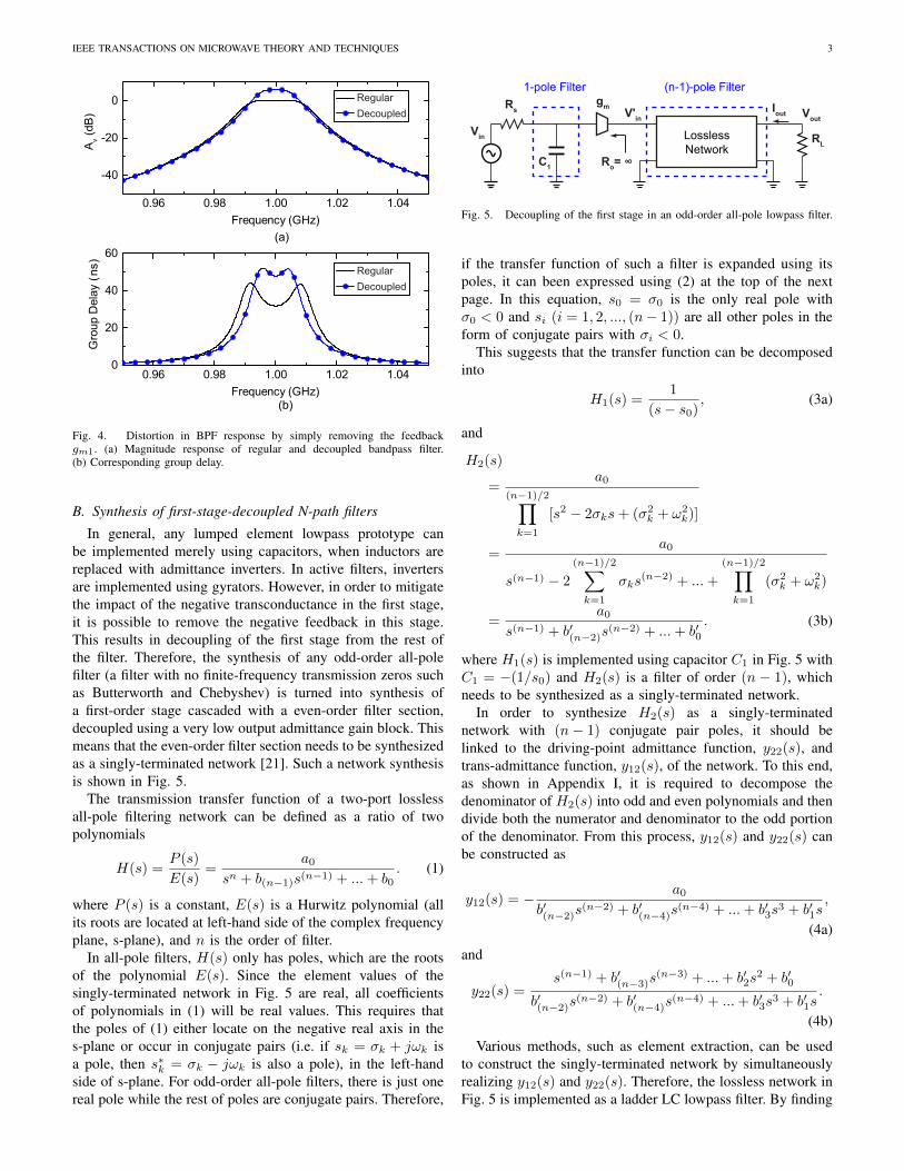
However, simply removing the feedback gm1, alters thebandwidth of the filter as well as the desired filter shape asshown in Fig. 4. As a result, a proper synthesis procedureis required to realize the filter with desired bandwidth andpassband shape while removing the negative gm cell in thefirst stage. A similar technique for decoupling the first stageis also showed in [8] to reduce the power consumption aswell as to reduce NF. However, due to the lack of a propersynthesis procedure of the filter, an extra feedback capacitor isused between input and output to maintain the passband rippleto a certain extent, which introduces stability concern in thefilter. In the next section, the proper synthesis procedure willbe discussed.
IEEE TRANSACTIONS ON MICROWAVE THEORY AND TECHNIQUES 3
(a)
(b)
RegularDecoupled
RegularDecoupled
ns
Fig. 4. Distortion in BPF response by simply removing the feedbackgm1. (a) Magnitude response of regular and decoupled bandpass filter.(b) Corresponding group delay.
B. Synthesis of first-stage-decoupled N-path filters
In general, any lumped element lowpass prototype canbe implemented merely using capacitors, when inductors arereplaced with admittance inverters. In active filters, invertersare implemented using gyrators. However, in order to mitigatethe impact of the negative transconductance in the first stage,it is possible to remove the negative feedback in this stage.This results in decoupling of the first stage from the rest ofthe filter. Therefore, the synthesis of any odd-order all-polefilter (a filter with no finite-frequency transmission zeros suchas Butterworth and Chebyshev) is turned into synthesis ofa first-order stage cascaded with a even-order filter section,decoupled using a very low output admittance gain block. Thismeans that the even-order filter section needs to be synthesizedas a singly-terminated network [21]. Such a network synthesisis shown in Fig. 5.
The transmission transfer function of a two-port losslessall-pole filtering network can be defined as a ratio of twopolynomials
H(s) =P (s)
E(s)=
a0
sn + b(n−1)s(n−1) + ...+ b0. (1)
where P (s) is a constant, E(s) is a Hurwitz polynomial (allits roots are located at left-hand side of the complex frequencyplane, s-plane), and n is the order of filter.
In all-pole filters, H(s) only has poles, which are the rootsof the polynomial E(s). Since the element values of thesingly-terminated network in Fig. 5 are real, all coefficientsof polynomials in (1) will be real values. This requires thatthe poles of (1) either locate on the negative real axis in thes-plane or occur in conjugate pairs (i.e. if sk = σk + jωk isa pole, then s∗k = σk − jωk is also a pole), in the left-handside of s-plane. For odd-order all-pole filters, there is just onereal pole while the rest of poles are conjugate pairs. Therefore,
Rsgm
C1
Vin RL
Vout
LosslessNetwork
Ro= ∞
1-pole Filter (n-1)-pole Filter
IoutV'in
Fig. 5. Decoupling of the first stage in an odd-order all-pole lowpass filter.
if the transfer function of such a filter is expanded using itspoles, it can been expressed using (2) at the top of the nextpage. In this equation, s0 = σ0 is the only real pole withσ0 < 0 and si (i = 1, 2, ..., (n− 1)) are all other poles in theform of conjugate pairs with σi < 0.
This suggests that the transfer function can be decomposedinto
H1(s) =1
(s− s0), (3a)
and
H2(s)
=a0
(n−1)/2∏k=1
[s2 − 2σks+ (σ2k + ω2
k)]
=a0
s(n−1) − 2
(n−1)/2∑k=1
σks(n−2) + ...+
(n−1)/2∏k=1
(σ2k + ω2
k)
=a0
s(n−1) + b′(n−2)s(n−2) + ...+ b′0
. (3b)
where H1(s) is implemented using capacitor C1 in Fig. 5 withC1 = −(1/s0) and H2(s) is a filter of order (n − 1), whichneeds to be synthesized as a singly-terminated network.
In order to synthesize H2(s) as a singly-terminatednetwork with (n− 1) conjugate pair poles, it should belinked to the driving-point admittance function, y22(s), andtrans-admittance function, y12(s), of the network. To this end,as shown in Appendix I, it is required to decompose thedenominator of H2(s) into odd and even polynomials and thendivide both the numerator and denominator to the odd portionof the denominator. From this process, y12(s) and y22(s) canbe constructed as
y12(s) = − a0
b′(n−2)s(n−2) + b′(n−4)s
(n−4) + ...+ b′3s3 + b′1s
,
(4a)
and
y22(s) =s(n−1) + b′(n−3)s
(n−3) + ...+ b′2s2 + b′0
b′(n−2)s(n−2) + b′(n−4)s
(n−4) + ...+ b′3s3 + b′1s
.
(4b)
Various methods, such as element extraction, can be usedto construct the singly-terminated network by simultaneouslyrealizing y12(s) and y22(s). Therefore, the lossless network inFig. 5 is implemented as a ladder LC lowpass filter. By finding

IEEE TRANSACTIONS ON MICROWAVE THEORY AND TECHNIQUES 4
H(s) =P (s)
E(s)=
a0
(s− s0)[(s− s1)(s− s∗1)(s− s2)(s− s∗2)...(s− s(n−1)/2)(s− s∗(n−1)/2)]
=a0
(s− s0)[(s2 − 2σ1s+ (σ21 + ω2
1)) · (s2 − 2σ2s+ (σ22 + ω2
2))...(s2 − 2σ(n−1)/2s+ (σ2(n−1)/2 + ω2
(n−1)/2))]
=a0
(s− s0)
(n−1)/2∏k=1
[s2 − 2σks+ (σ2k + ω2
k)]
.
(2)
the element values of the network, the synthesis is completed.Appendix I shows a recursive method for realizing such anetwork.
In order to completely realize the filter using only capaci-tors, the series inductors, Lk, are replaced by shunt capacitors,Ck, and admittance inverters, Jk. The value of admittance in-verters (also known as J-inverters), which can be implementedusing gyrators, gmk, are found from
J2k = g2
mk =CkLk
. (5)
Finally, since the coupling matrix of a bandpass filter isthe same as ones of its lowpass prototype [22], the decoupledlowpass filter can be readily transformed to a bandpass filter,without changing the coupling values. It is accomplishedusing converting the shunt capacitors to shunt LC resonatorsaccording to
Lk =1
ω2oCk
, (6)
where ωo = 2πf0 is the center frequency of the bandpassfilter in rad/sec. Fig. 6 summarizes all the steps required forsynthesizing of an all-pole filter with a decoupled first stage.
C. Design Example
In this section, a fifth-order Butterworth lowpass filter issynthesized in the form of a decoupled single-pole stageand a singly-terminated fourth-pole portion, as an example todemonstrate how the above method is used.
In the case of odd-order Butterworth filters, H1(s) andH2(s), defined in (3a) and (3b) respectively, are simplifiedto
H1(s) =1
(s+ 1), (7a)
and
H2(s) =1
(n−1)/2∏k=1
[s2 + 2 sin(θk)s+ 1]
, (7b)
where θk is the angle between two consequence poles [23]and is calculated using
θk = (2k − 1)π
2nk = 1, 2, ..., n. (8)
Construct y12(s) and y22(s) from H2(s) by decomposing its denominator into odd and even polynomials and then
dividing its numerator to the odd portion of the denominator polynomial.
The transmission response of a singly-terminated function istied to its trans-admittance,
y12(s), and driving-pointadmittance, y22(s) functions.
Realize the lowpass prototype in the form of a LC laddernetwork using element extraction or similar methods.
The function H1(s) is implemented as a shunt capacitor following by a low output admittance
gain block. Therefore, the function H2(s) must be
implemented as a singly-terminated network.
Replace the series inductors with shunt capacitors and admittance inverters using (5) to fully implement the filter
using only capacitors.
Transform the lowpass prototype to a bandpass filter byconverting the shunt capacitors to shunt LC resonators
using (6).
Start with the transmission transfer function, H(s), of the filter.
Decompose the transfer function into functions with areal pole, H1(s) and (n-1) conjugate pairs, H2(s).
single
Fig. 6. Required steps for synthesis of a filter with a decoupled first stage.
C1 C3RL
VoutL2
Rsgm
C5
Vin
Ro= ∞
1-pole Filter 4-pole Filter
L4
Fig. 7. 5th-order Butterworth lowpass filter with a decoupled first stage.
IEEE TRANSACTIONS ON MICROWAVE THEORY AND TECHNIQUES 5
(b)
(c)
(a)
(e)
(f)
gm1 gm3
-gm3 C'1 L'1C1 C2 C3
gm2
-gm2 C4 C5
gm4
-gm4
gm1 gm3
-gm3
gm2
-gm2
gm3
-gm3C'2 L'2 C'3 L'3 C'4 L'4 C'5 L'5
(d)
50 Ω
50 Ω
1 Ω
1 Ω
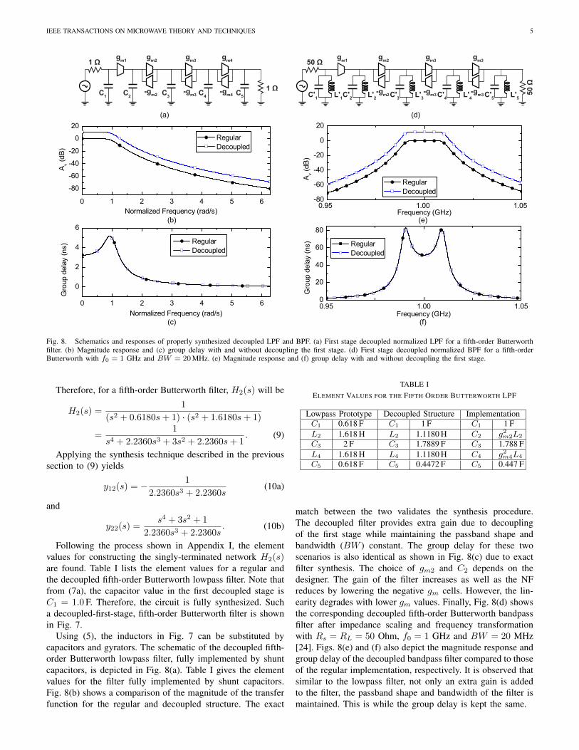
Fig. 8. Schematics and responses of properly synthesized decoupled LPF and BPF. (a) First stage decoupled normalized LPF for a fifth-order Butterworthfilter. (b) Magnitude response and (c) group delay with and without decoupling the first stage. (d) First stage decoupled normalized BPF for a fifth-orderButterworth with f0 = 1 GHz and BW = 20 MHz. (e) Magnitude response and (f) group delay with and without decoupling the first stage.
Therefore, for a fifth-order Butterworth filter, H2(s) will be
H2(s) =1
(s2 + 0.6180s+ 1) · (s2 + 1.6180s+ 1)
=1
s4 + 2.2360s3 + 3s2 + 2.2360s+ 1. (9)
Applying the synthesis technique described in the previoussection to (9) yields
y12(s) = − 1
2.2360s3 + 2.2360s(10a)
and
y22(s) =s4 + 3s2 + 1
2.2360s3 + 2.2360s. (10b)
Following the process shown in Appendix I, the elementvalues for constructing the singly-terminated network H2(s)are found. Table I lists the element values for a regular andthe decoupled fifth-order Butterworth lowpass filter. Note thatfrom (7a), the capacitor value in the first decoupled stage isC1 = 1.0 F. Therefore, the circuit is fully synthesized. Sucha decoupled-first-stage, fifth-order Butterworth filter is shownin Fig. 7.
Using (5), the inductors in Fig. 7 can be substituted bycapacitors and gyrators. The schematic of the decoupled fifth-order Butterworth lowpass filter, fully implemented by shuntcapacitors, is depicted in Fig. 8(a). Table I gives the elementvalues for the filter fully implemented by shunt capacitors.Fig. 8(b) shows a comparison of the magnitude of the transferfunction for the regular and decoupled structure. The exact
TABLE IELEMENT VALUES FOR THE FIFTH ORDER BUTTERWORTH LPF
Lowpass Prototype Decoupled Structure ImplementationC1 0.618 F C1 1 F C1 1 FL2 1.618 H L2 1.1180 H C2 g2m2L2
C3 2 F C3 1.7889 F C3 1.788 FL4 1.618 H L4 1.1180 H C4 g2m4L4
C5 0.618 F C5 0.4472 F C5 0.447 F
match between the two validates the synthesis procedure.The decoupled filter provides extra gain due to decouplingof the first stage while maintaining the passband shape andbandwidth (BW ) constant. The group delay for these twoscenarios is also identical as shown in Fig. 8(c) due to exactfilter synthesis. The choice of gm2 and C2 depends on thedesigner. The gain of the filter increases as well as the NFreduces by lowering the negative gm cells. However, the lin-earity degrades with lower gm values. Finally, Fig. 8(d) showsthe corresponding decoupled fifth-order Butterworth bandpassfilter after impedance scaling and frequency transformationwith Rs = RL = 50 Ohm, f0 = 1 GHz and BW = 20 MHz[24]. Figs. 8(e) and (f) also depict the magnitude response andgroup delay of the decoupled bandpass filter compared to thoseof the regular implementation, respectively. It is observed thatsimilar to the lowpass filter, not only an extra gain is addedto the filter, the passband shape and bandwidth of the filter ismaintained. This is while the group delay is kept the same.

IEEE TRANSACTIONS ON MICROWAVE THEORY AND TECHNIQUES 6
Rs
C1 L1 C2 L2
Vin
C3 L3
RL
VoutJs,1 J1,2 J2,3 J3,L
gm1 gm2
-gm3
Rs
C1 L1 C2 L2
Vin
C3 L3
RL
VoutJs,1 J3,L
gm1 gm2
-gm3
Rs
C1 L1 C2 L2
Vin
C3 L3
RL
Vout
Cb
-Ca -Ca
Cb
gm1 gm2
-gm3
Rs
L1 C2 L2
Vin
C3-Ca L3
RL
Vout
Cb Cb
C1-Ca
(a)
(b)
(c)
(d)
(e)
C'1 L1
gm1 gm2
-gm3C2 L2 C'3 L3
Cb Cb
Rs
RL
Vout
Vin
Fig. 9. Reconfiguring a Butterworth filter to a Chebyshev filter with variablebandwidth. (a) A Butterworth filter can be transformed to a similar bandwidthChebyshev filter using gyrators/J-inverters. (b) Decoupling the first stage.(c) Implementation of source and load J-inverters. (d) The negative capacitanceis absorbed in C1 and C3. (e) Component tunability to obtain desired filterresponse.
III. TUNABLE FILTER BANDWIDTH AND SHAPE
It is often desirable to reconfigure the filter shape andbandwidth as well as the center frequency of the filter to copewith the dynamic environment [25]–[27].
In coupled-resonator filters, such as the one shown inFig. 9(a), the filter bandwidth is predominantly determined bythe inter-resonator couplings if identical resonators are used. Inthe proposed N-path filter design, the inter-resonator couplingis realized by active gyrators (J-inverter) consisting of back-to-back connected transconductance amplifiers (Fig. 9(b)). Theinverter value can be changed by changing the gm value ofthe gyrator. However, this approach results in significant trade-off between the bandwidth and the power consumption of thefilter; more power is needed for larger bandwidth. To resolvethis issue, it is opted to tune resonators in this work. In terms ofN-path filter implementation, this means tuning the basebandcapacitors CBx in Fig. 2(c).
In addition to tuning the internal couplings, the externalcouplings also need to be adjusted to transform the filter shapeor bandwidth with proper matching, while maintaining the C1
-CaR
CbJ
R ≡
Fig. 10. A possible way for implementation of J-inverters in integratedcircuits.
TABLE IIELEMENT VALUES FOR A THIRD ORDER BUTTERWORTH LPF WITH
40 MHZ BANDWIDTH
Lowpass Prototype Denormalized LPF Decoupled FirstStage
C1 1 C1 79.57 pF C1 79.57 pFL2 2 L2 397.88 nF C2 9.94 pFC3 1 C3 79.57 pF C3 79.57 pF
& C3 constant. This can be achieved by placing inverters atthe ports (that is JS,1 and J3,L in Fig. 9(a)). These invertersare essentially impedance transformers and are used to scalethe source and load impedances to arbitrary values. Theycan also be realized by a stacked capacitor transformer foreasy on-chip integration as shown in Fig. 10. Fig. 9(c) showshow the external couplings in the coupled-resonator filter arereplaced with the stacked capacitor transformer. The values ofthe capacitors can be readily calculated from
Cb =J
ωo√
(1− (JR)2)(11a)
and
Ca =−J√
(1− (JR)2)
ωo, (11b)
where J is either JS,1 or J3,L as in Fig. 9(a). The negative Cacan be absorbed in C1 or C3 as shown in Fig. 9(d). In practice,Ca is much smaller than both C1 and C3. To implement atunable bandwidth, Cb and C2 need to be adjusted.
To understand the range of values for the tuning compo-nents, a design example is given here for a third order filterwith a variable bandwidth from 20 MHz to 40 MHz, whoseshape can be reconfigured between a Butterworth responseand a Chebyshev one with arbitrary ripple levels. The nominalvalues of the components for a Butterworth lowpass filterconfiguration with 40 MHz bandwidth is listed in Table. II.C2 is calculated from (32b) for gm2 = 10 mS, gm3 = 5 mSand corresponding L2. The LPF can then be transformed intoa BPF using (6). The schematic of the filter follows Fig. 9(e).
The coupling capacitor Cb is varied based on the frequencyand bandwidth requirements. Fig. 11 shows the calculated re-quired component values for a Butterworth configuration withvarious bandwidth. The coupling capacitor Cb is calculated at0.2 GHz and 1 GHz to cover the whole tuning range. As thefrequency changes from 0.2 GHz to 1 GHz, Cb needs to bechanged from 3.18 pF to 42.1 pF. The nominal values of thecapacitors are chosen based on the Butterworth configurationwith 40 MHz bandwidth. Therefore, Cb is not required for that

IEEE TRANSACTIONS ON MICROWAVE THEORY AND TECHNIQUES 7
gm1
S1CB1
S3
S3
S1
S1
S3
S3
S1
gm2
S1
S3
S3
S1
gm2
-gm3
00
1800∑
∆
gm1
50 Ω ro1
ro1
ro2
ro2
8X
3X3X
8X
Rf
2X
2X
VDD
1
VDD
1
2X
2X
Cb
Cb
50 Ω
00
1800 ∑
∆
50 Ω
50 Ω
CHIP BORDER
CB2 CB3
Fig. 13. Full implementation of the proposed filter.
Cap
acita
nce
Fig. 11. Component values of the proposed filter as Butterworth configurationwith different bandwidth. Cb is calculated at f0 = 0.2 GHz and 1 GHz.
0.0 0.5 1.0 1.5 2.0 2.5 3.0 3.50
20
40
60
80
C1=C3, C2
(pF)
Ripple (dB)
Cap
acita
nce
Fig. 12. Component values of the proposed filter as Chebyshev configurationwith different ripple level. Cb is calculated at f0 = 0.2 GHz and 1 GHz.
configuration (no point for Cb in Fig.11 for BW = 40 MHz)or in other words, Cb is shorted with the top switch in Fig. 9(e).As a result, the filter looks similar as Fig. 8(d) for this specificconfiguration.
In a similar fashion, by adjusting C1(= C3), C2, Ca, andCb, it is possible to reconfigure the filter into a Chebyshevresponse with different ripple levels. Fig. 12 shows the re-quired component values for the Chebyshev configuration with40 MHz bandwidth and different ripple level.
The parallel LC tanks can be realized with N-path filters,where the center frequency is determined by the clock fre-quency. The corresponding baseband capacitors CB1(= CB3)and CB2 in Fig. 2(c) can be calculated from [12]
CBx = Cxm[N sin2(πD) +Dπ2(1−ND)
]NDπ2
, (12)
where m = 2 for the single-ended circuit and m = 8 for thedifferential network. In a lumped prototype, the absorptionof Ca into C1 has two effects. It changes both the centerfrequency and the bandwidth of the resonators. However, on
0 5 10 15 20 25 30 35 40
40
60
80
100
120C2
Cb@ 1 GHz
Cb@ 0.2 GHz
Capacitor (pF)
Fig. 14. Quality factor for the tuning capacitors C2 at 1 GHz and Cb at0.2 GHz and 1 GHz.
the other side, in a N-path implementation the absorption ofthe negative capacitance only changes the bandwidth of theresonator as the center frequency is determined primarily bythe clock frequency. Therefore, there can be a slight differencebetween the lumped prototype and the actual implementationin terms of filter BW. However, the filter BW can be adjustedby tuning either Cb or C2.
IV. FILTER IMPLEMENTATION
The full implementation of the proposed filter is shown inFig. 13. Large NMOS RF switches of W/L = 80µm/60nm(on-resistance of approximately 4.2 Ω) are used to reduce thenoise, non-linearity and mismatch between them. The switchesare driven by 25% duty cycle 4-phase non-overlapping clocks.A differential structure is exploited for the proposed archi-tecture to suppress common-mode disturbance as well as thedifferential baseband capacitors reduce the total area. MIMcapacitor with underlying metal are used for the basebandcapacitors. The resistors are realized with N+ poly resistorwithout silicide. Each switch is biased at 900-mV DC voltage(VCLK) to provide full 1.2-V swing to maximize the linearityof the switches. Instead of using a single varactor, a switched-bank of capacitor is used to implement Cb for maintaining areasonable Q. Fig. 14 shows the Q for the tuning capacitorsC2 at 1 GHz and Cb at 0.2 GHz and 1 GHz. The simulatedQ of the switched capacitor bank ranges from 40 to 100.Within this Q range, the insertion loss degradation is less than1 dB. This insertion loss variation can be compensated bygain adjustments through the gm cells. The negative gm3 inFig. 9(e) can be easily implemented by flipping the connectionin a differential configuration.
The switch size used along with Cb is 120µm/60 nm, withan on-resistance of 3.6 Ω and Coff of 42.3 fF. The choice of
IEEE TRANSACTIONS ON MICROWAVE THEORY AND TECHNIQUES 8
TABLE IIIFILTER PERFORMANCE BASED ON DIFFERENT PARAMETERS
Parameter Gain NF IIP3 BW Power
gm1 ↑ ↑ ↓ ↓ – ↑gm2 ↑ – ↓ ↑ ↑ ↑gm3 ↑ ↓ ↑ ↑ ↑ ↑
(a) (b)
0.750.06
1.750.06
×32
×32
(c)
Vin
VDD
Vout
0.60.06
1.40.06
×8
×8
Vin
VDD
Vout
0.60.06
1.40.06
×4
×4
Vin
VDD
Vout
Fig. 15. Configuration of gm cells. (a) gm1, (b) gm2, and (c) gm3.
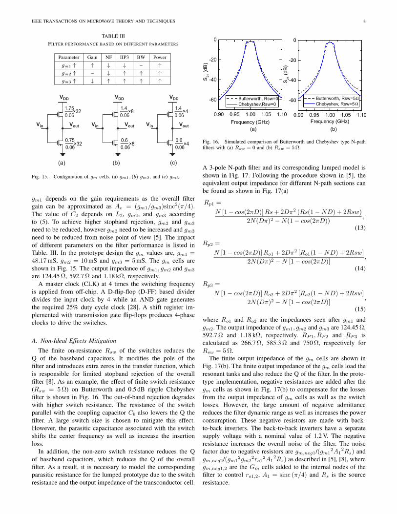
gm1 depends on the gain requirements as the overall filtergain can be approximated as Av = (gm1/gm3)sinc2(π/4).The value of C2 depends on L2, gm2, and gm3 accordingto (5). To achieve higher stopband rejection, gm2 and gm3
need to be reduced, however gm2 need to be increased and gm3
need to be reduced from noise point of view [5]. The impactof different parameters on the filter performance is listed inTable. III. In the prototype design the gm values are, gm1 =48.17 mS, gm2 = 10 mS and gm3 = 5 mS. The gm cells areshown in Fig. 15. The output impedance of gm1, gm2 and gm3
are 124.45 Ω, 592.7 Ω and 1.18 kΩ, respectively.A master clock (CLK) at 4 times the switching frequency
is applied from off-chip. A D-flip-flop (D-FF) based dividerdivides the input clock by 4 while an AND gate generatesthe required 25% duty cycle clock [28]. A shift register im-plemented with transmission gate flip-flops produces 4-phaseclocks to drive the switches.
A. Non-Ideal Effects Mitigation
The finite on-resistance Rsw of the switches reduces theQ of the baseband capacitors. It modifies the pole of thefilter and introduces extra zeros in the transfer function, whichis responsible for limited stopband rejection of the overallfilter [8]. As an example, the effect of finite switch resistance(Rsw = 5 Ω) on Butterworth and 0.5 dB ripple Chebyshevfilter is shown in Fig. 16. The out-of-band rejection degradeswith higher switch resistance. The resistance of the switchparallel with the coupling capacitor Cb also lowers the Q thefilter. A large switch size is chosen to mitigate this effect.However, the parasitic capacitance associated with the switchshifts the center frequency as well as increase the insertionloss.
In addition, the non-zero switch resistance reduces the Qof baseband capacitors, which reduces the Q of the overallfilter. As a result, it is necessary to model the correspondingparasitic resistance for the lumped prototype due to the switchresistance and the output impedance of the transconductor cell.
(a) (b)
ΩΩ
Fig. 16. Simulated comparison of Butterworth and Chebyshev type N-pathfilters with (a) Rsw = 0 and (b) Rsw = 5 Ω.
A 3-pole N-path filter and its corresponding lumped model isshown in Fig. 17. Following the procedure shown in [5], theequivalent output impedance for different N-path sections canbe found as shown in Fig. 17(a)
Rp1 =
N [1− cos(2πD)]Rs+ 2Dπ2 (Rs(1−ND) + 2Rsw)
2N(Dπ)2 −N(1− cos(2πD)),
(13)
Rp2 =
N [1− cos(2πD)]Ro1 + 2Dπ2 [Ro1(1−ND) + 2Rsw]
2N(Dπ)2 −N [1− cos(2πD)],
(14)
Rp3 =
N [1− cos(2πD)]Ro2 + 2Dπ2 [Ro2(1−ND) + 2Rsw]
2N(Dπ)2 −N [1− cos(2πD)],
(15)
where Ro1 and Ro2 are the impedances seen after gm1 andgm2. The output impedance of gm1, gm2 and gm3 are 124.45 Ω,592.7 Ω and 1.18 kΩ, respectively. RP1, RP2 and RP3 iscalculated as 266.7 Ω, 585.3 Ω and 750 Ω, respectively forRsw = 5 Ω.
The finite output impedance of the gm cells are shown inFig. 17(b). The finite output impedance of the gm cells load theresonant tanks and also reduce the Q of the filter. In the proto-type implementation, negative resistances are added after thegm cells as shown in Fig. 17(b) to compensate for the lossesfrom the output impedance of gm cells as well as the switchlosses. However, the large amount of negative admittancereduces the filter dynamic range as well as increases the powerconsumption. These negative resistors are made with back-to-back inverters. The back-to-back inverters have a separatesupply voltage with a nominal value of 1.2 V. The negativeresistance increases the overall noise of the filter. The noisefactor due to negative resistors are gm,neg1/(gm1
2A12Rs) and
gm,neg2/(gm12gm2
2ro12A1
2Rs) as described in [5], [8], wheregm,neg1,2 are the Gm cells added to the internal nodes of thefilter to control ro1,2, A1 = sinc (π/4) and Rs is the sourceresistance.

IEEE TRANSACTIONS ON MICROWAVE THEORY AND TECHNIQUES 9
(a)
(b)
(c)
(d)
C1 L1
gm1 gm2
-gm3C2 L2 C3 L3
50 Ω
50 ΩRp1 Rp2 Rp3
gm1 gm2
-gm3.........
S1 S2 S3 SN
CBB1
.........
S1 S2 S3 SN
CBB2
50 Ω
50 Ω
-Rg1 .........
S1 S2 S3 SN
CBB3
-Rg2
Fig. 17. Effect of finite output impedance of gm cell and the utilized solution. (a) Lumped model of a 3-pole N-path filter with finite output impedance ofthe gm cells loading the tanks. (b) Negative resistances are added to compensate for the loading. (c) S21 for both cases. (d) Group delay for both cases.
Rsgm1
Vin
gm2
-gm3 r’o2
VoutIS IF
IO
VX
r’o1
Fig. 18. Simplified model used to calculate the IIP3 of the filter.
B. Linearity Analysis
It is highly desirable for a front-end filter to be extremelylinear to tackle strong out-of-band blockers. In an long-term-evolution (LTE) receiver, for example, transmit leakageintroduces a out-of-band (OOB) blocker at different frequencyoffset to primary and diversity receivers which places stringentlinearity and power handling capability requirement for thefront-end filter. In this section, the linearity of the proposedfilter is derived using the simple equivalent model shown inFig. 18.
Writing equations at the Vout node, by considering the firstand the third non-linear terms, yields
gm2,1Vx + gm2,3V3x + go2Vout + go2V
3out = 0 (16)
where gmx,1 and gmx,3 are the transconductance of gm cellsassociated with the first and third harmonics. r′o1 is thecombined resistance of ro1, RP2 and −Rg1. Similarly, r′o2 isthe combined resistance of ro2, RP3, RL and −Rg2.The feedback current at the gate of gm2 can also be expressedas
IF = −gm3,1Vout − gm3,3V3out. (17)
The output current of gm1 is
Is = −gm1,1Vin − gm1,3V3in. (18)
It is possible to represent the output voltage Vout as (seeAppendix)
Vout = α1Vin + α3V3in, (19)
where
α1 =gm1,1
gm3,1 +1
gm2,1r′o1r′o2
, (20)
and
α3 =gm1,3
gm3,1 + 1gm2,1r′o1r
′o2
−
(gm1,1
gm3,1 + 1gm2,1r′o1r
′o2
)3
×A− gm2,3r
′o2
g4m2,1r
′o1r′o2
4(
1gm2,1r′o1r
′o2
+ gm3,1
),where A = g4
m2,1gm3,3r′o1r′o2
4 − g3m2,1r
′o2
3.
Assuming gm3,1 1
gm2,1r′o1r′o2
,
Vout =
gm1,1
gm3,1Vin +
(gm1,3
gm3,3+gm1,13
gm3,13
×A− gm2,3r
′o2
g4m2,1gm3,1r′o1r
′o2
4
)V 3in
(21)
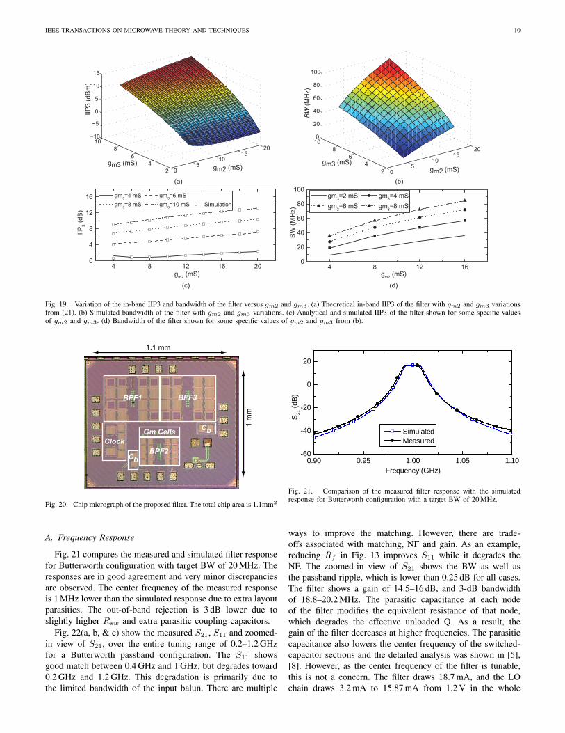
The in-band input referred third order intercept point (IIP3)calculated based on (21) with variations in gm2 and gm3 isshown in Fig. 19 (a). The IIP3 increases with increase in bothgm2 and gm3. Fig. 19 (b) shows the simulated bandwidth ofthe filter with gm2 and gm3. The bandwidth also increaseswith higher gm2, gm3. However, by increasing gm2 and gm3,power consumption increases and the gain of the filter drops.In terms of noise, it is required to increase gm2 and reducegm3 [14].
V. MEASUREMENT RESULTS
The filter is fabricated in a 65-nm CMOS technology. Thechip has an area of 1.1 mm2 including the bond pads (Fig. 20).The circuit is wire-bonded and tested on a printed circuitboard. An off-chip balun (MACOM MABA-010247-2R1250)is used to transform a single-ended signal to a differentialsignal. The typical insertion loss of the balun is approximately1 dB.
IEEE TRANSACTIONS ON MICROWAVE THEORY AND TECHNIQUES 10
(a) (b)0
510
1520
24
68
10−10
−5
0
5
10
15
gm2 (mS)gm3 (mS)
IIP3
(dBm
)
05
1015
20
24
68
100
20
40
60
80
100
gm2 (mS)gm3 (mS)
BW (M
Hz)
(c) (d)
gm2 (mS) gm2 (mS)
Fig. 19. Variation of the in-band IIP3 and bandwidth of the filter versus gm2 and gm3. (a) Theoretical in-band IIP3 of the filter with gm2 and gm3 variationsfrom (21). (b) Simulated bandwidth of the filter with gm2 and gm3 variations. (c) Analytical and simulated IIP3 of the filter shown for some specific valuesof gm2 and gm3. (d) Bandwidth of the filter shown for some specific values of gm2 and gm3 from (b).
Clock
BPF1 BPF3
BPF2Cb
CbGm Cells
1.1 mm
1 m
m
Fig. 20. Chip micrograph of the proposed filter. The total chip area is 1.1mm2
A. Frequency Response
Fig. 21 compares the measured and simulated filter responsefor Butterworth configuration with target BW of 20 MHz. Theresponses are in good agreement and very minor discrepanciesare observed. The center frequency of the measured responseis 1 MHz lower than the simulated response due to extra layoutparasitics. The out-of-band rejection is 3 dB lower due toslightly higher Rsw and extra parasitic coupling capacitors.
Fig. 22(a, b, & c) show the measured S21, S11 and zoomed-in view of S21, over the entire tuning range of 0.2–1.2 GHzfor a Butterworth passband configuration. The S11 showsgood match between 0.4 GHz and 1 GHz, but degrades toward0.2 GHz and 1.2 GHz. This degradation is primarily due tothe limited bandwidth of the input balun. There are multiple
0 . 9 0 0 . 9 5 1 . 0 0 1 . 0 5 1 . 1 0- 6 0
- 4 0
- 2 0
0
2 0
S i m u l a t e d M e a s u r e d
S 21 (d
B)
F r e q u e n c y ( G H z )
Fig. 21. Comparison of the measured filter response with the simulatedresponse for Butterworth configuration with a target BW of 20 MHz.
ways to improve the matching. However, there are trade-offs associated with matching, NF and gain. As an example,reducing Rf in Fig. 13 improves S11 while it degrades theNF. The zoomed-in view of S21 shows the BW as well asthe passband ripple, which is lower than 0.25 dB for all cases.The filter shows a gain of 14.5–16 dB, and 3-dB bandwidthof 18.8–20.2 MHz. The parasitic capacitance at each nodeof the filter modifies the equivalent resistance of that node,which degrades the effective unloaded Q. As a result, thegain of the filter decreases at higher frequencies. The parasiticcapacitance also lowers the center frequency of the switched-capacitor sections and the detailed analysis was shown in [5],[8]. However, as the center frequency of the filter is tunable,this is not a concern. The filter draws 18.7 mA, and the LOchain draws 3.2 mA to 15.87 mA from 1.2 V in the whole

IEEE TRANSACTIONS ON MICROWAVE THEORY AND TECHNIQUES 11
(b)
(c)
(zoo
med
) 16
14
12
10200 400
(a)
600 800 1000 1200
20M 20.1M 20.2M 20.1M 20.4M 20.5M
-7.8 dB
-13 dB -13.5 dB -12.9 dB -14.5 dB
-8.8 dB
M
Fig. 22. Measured response of the proposed filter configured as Butterworthtype over the whole tuning range for a target bandwidth of 20 MHz, (a) S21
at uniformly-spaced center frequencies, (b) corresponding S11 with themaximum depths labelled, and (c) zoomed-in view of the passband responseto clearly show the BW. Each window corresponds to a frequency span of40 MHz.
tuning range. The clock buffer power consumption is 13.4 mW.The LO feedthrough to the input port of the filter is −65 dBmat a center frequency of 1 GHz.
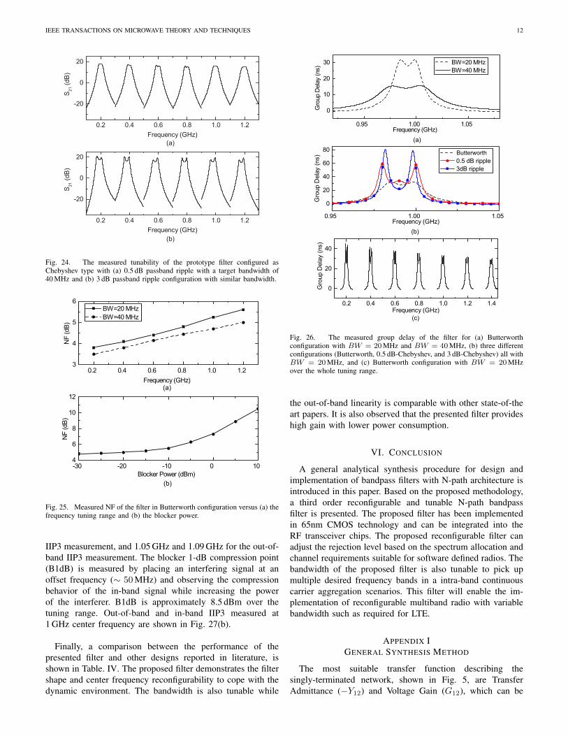
The proposed filter can be reconfigured in Butterworth,Chebyshev-0.5 dB ripple and Chebyshev-3 dB ripple withproper tuning of Cb and C2. For example, the tunability of theproposed filter for 0.5-dB ripple Chebyshev configuration isshown in Fig. 23(a) for 20-MHz bandwidth. Fig. 23(b) showsthe close-in response at 1 GHz with different ripple levels. Itis possible to increase the stopband rejection of the filter withhigher passband ripple.
The filter can also be reconfigured in terms of bandwidth.For example, Fig. 24 shows the filter response for bothButterworth and Chebyshev-3 dB ripple configuration withtarget bandwidth of 40 MHz. The filter has more loss at higherfrequencies due to gm cells. The primary objective of theproposed filter is to reconfigure it smartly based on spectrumrequirements.
B. Noise Figure
The measured NF of the filter over the tuning range is shownin Fig. 25(a) for two different bandwidths. The filter has ameasured small signal NF of 3.7–5.5 dB over the tuning rangeof 0.2–1.2 GHz for BW = 40 MHz. The NF increases as thebandwidth decreases due to the finite Q and switch loss of Cb.The NF is higher at high frequencies as the gain of the filterdecreases.
(b)
(a)
Butterworth
Fig. 23. Measured S21 of the prototype filter. (a) Configured as Chebyshevtype with 0.5 dB passband ripple for a target bandwidth of 20 MHz, tunedacross the tuning rang. (b) Close-in response of the filter for three differentconfigurations (Butterworth, 0.5 dB-Chebyshev, and 3 dB-Chebyshev ) at1 GHz.
Measured NF with various blocker power level is shown inFig. 25(b) with f0 = 1 GHz. In this test, the blocker is placedat 50 MHz offset. The NF increases with increasing blockerpower due to reciprocal mixing of the blocker and the LOphase noise. The external LO signals (Keysight E8663D) havean SSB phase noise of -143 dBc/Hz at 100 KHz offset. Thesimulated phase-noise of on-chip 4-phase LO signals (S1, S2,S3 and S4) with frequency of 1 GHz from the noisy externalsignal generator is around -150 dBc/Hz at 100 KHz offset.When the blocker mixes with LO phase noise, it depositsadditional noise in the receive channel proportional to theblocker amplitude. The proposed filter can tolerate an 10-dBmblocker with NF<10 dB.
C. Group Delay
The measured group delay (GD) of the filter is shown inFig. 26. The group delay for the Butterworth configurationwith different bandwidths is shown in Fig. 26(a) as the GD isinversely proportional to the filter bandwidth. Fig. 26(b) showsthe GD for different filter configuration and BW = 20 MHz.The GD of the filter over the whole tuning range is shownin Fig. 26(c), where the filter is configured for Butterworthtype and BW = 20 MHz. This highlights the efficacy of thefilter in controlling signal delay characteristics. The GD willbe reduced for higher bandwidth.
D. Linearity
To evaluate the linearity of the filter, two-tone IIP3 andcompression measurements were carried out and results areshown in Fig. 27(a&b). With the filter tuned to 1 GHz, the twotones are placed at 1.008 GHz and 1.01 GHz for the in-band
IEEE TRANSACTIONS ON MICROWAVE THEORY AND TECHNIQUES 12
(a)
(b)
Fig. 24. The measured tunability of the prototype filter configured asChebyshev type with (a) 0.5 dB passband ripple with a target bandwidth of40 MHz and (b) 3 dB passband ripple configuration with similar bandwidth.
(a)
(b)
Fig. 25. Measured NF of the filter in Butterworth configuration versus (a) thefrequency tuning range and (b) the blocker power.
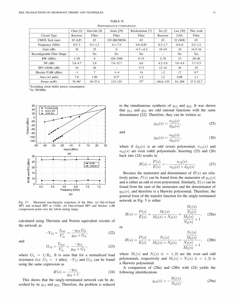
IIP3 measurement, and 1.05 GHz and 1.09 GHz for the out-of-band IIP3 measurement. The blocker 1-dB compression point(B1dB) is measured by placing an interfering signal at anoffset frequency (∼ 50 MHz) and observing the compressionbehavior of the in-band signal while increasing the powerof the interferer. B1dB is approximately 8.5 dBm over thetuning range. Out-of-band and in-band IIP3 measured at1 GHz center frequency are shown in Fig. 27(b).
Finally, a comparison between the performance of thepresented filter and other designs reported in literature, isshown in Table. IV. The proposed filter demonstrates the filtershape and center frequency reconfigurability to cope with thedynamic environment. The bandwidth is also tunable while
(a)
(b)
(c)
Butterworth
Fig. 26. The measured group delay of the filter for (a) Butterworthconfiguration with BW = 20 MHz and BW = 40 MHz, (b) three differentconfigurations (Butterworth, 0.5 dB-Chebyshev, and 3 dB-Chebyshev) all withBW = 20 MHz, and (c) Butterworth configuration with BW = 20 MHzover the whole tuning range.
the out-of-band linearity is comparable with other state-of-theart papers. It is also observed that the presented filter provideshigh gain with lower power consumption.
VI. CONCLUSION
A general analytical synthesis procedure for design andimplementation of bandpass filters with N-path architecture isintroduced in this paper. Based on the proposed methodology,a third order reconfigurable and tunable N-path bandpassfilter is presented. The proposed filter has been implementedin 65nm CMOS technology and can be integrated into theRF transceiver chips. The proposed reconfigurable filter canadjust the rejection level based on the spectrum allocation andchannel requirements suitable for software defined radios. Thebandwidth of the proposed filter is also tunable to pick upmultiple desired frequency bands in a intra-band continuouscarrier aggregation scenarios. This filter will enable the im-plementation of reconfigurable multiband radio with variablebandwidth such as required for LTE.
APPENDIX IGENERAL SYNTHESIS METHOD
The most suitable transfer function describing thesingly-terminated network, shown in Fig. 5, are TransferAdmittance (−Y12) and Voltage Gain (G12), which can be
IEEE TRANSACTIONS ON MICROWAVE THEORY AND TECHNIQUES 13
TABLE IVPERFORMANCE COMPARISON.
Chen [2] Darvishi [8] Amin [29] Reiskarimian [7] Xu [3] Luo [30] This work
Circuit Type Receiver Filter Filter Filter Receiver LNA Filter
CMOS Tech (nm) 65 (LP) 65 130 (BiCMOS) 65 65 32 (SOI) 65
Frequency (GHz) 0.5–3 0.1–1.2 4.1–7.9 0.6–0.85 0.3–1.7 0.4–6 0.2–1.2
Gain (dB) 38 25 0 -4.7∼-6.2 19–34 10 14.5–16
Reconfigurable Filter Shape – No No No – No Yes
BW (MHz) 1–30 8 120–1500 9–15 2–76 15 20–40
NF (dB) 3.8–4.7 2.8 7.6–15.7 8.6 4.2–5.6 3.6–4.9 3.7–5.5
IIP3 (OOB) (dB) 10 26 – 17.5 12–14 36 25
Blocker P1dB (dBm) -1 7 -1–4 14 >2 17 8.7
Area (w/ pads) 7.8 1.96 0.37 1.2 1.2 0.88 1.1
Power (mW) 76–961 18–57.4 112–125 752 146.6–155 81–209 37.5–52.71Excluding clock buffer power consumption2At 700 MHz
(a)
(b)
Fig. 27. Measured non-linearity responses of the filter. (a) Out-of-bandIIP3 and in-band IIP3 at 1 GHz. (b) Out-of-band IIP3 and blocker 1-dBcompression point over the whole tuning range.
calculated using Thevenin and Norton equivalent circuits ofthe network as
−Y12 =IoutV ′in
=−y12.GLy22 +GL
, (22)
andG12 =
VoutV ′in
=−y12
y22 +GL, (23)
where GL = 1/RL. It is seen that for a normalized loadresistance (i.e. GL = 1 mho), −Y12 and G12 can be foundusing the same expression as
H(s) =−y12
y22 + 1. (24)
This shows that the singly-terminated network can be de-scribed by its y12 and y22. Therefore, the problem is reduced
to the simultaneous synthesis of y12 and y22. It was shownthat y12 and y22 are odd rational functions with the samedenominator [22]. Therefore, they can be written as
y12(s) =n12(s)
d22(s), (25)
andy22(s) =
n22(s)
d22(s), (26)
where if d22(s) is an odd (even) polynomial, n12(s) andn22(s) are even (odd) polynomials. Inserting (25) and (26)back into (24) results in
H(s) =P (s)
E(s)= − n12(s)
n22(s) + d22(s). (27)
Because the numerator and denominator of H(s) are rela-tively prime, P (s) can be found from the numerator of y12(s)and is either an odd or even polynomial. Similarly, E(s) can befound from the sum of the numerator and the denominator ofy22(s), and therefore is a Hurwitz polynomial. Therefore, thegeneral form of the transfer function for the singly-terminatednetwork in Fig. 5 is either
H(s) =P (s)
E(s)=
M1(s)
M2(s) +N2(s)=
M1(s)
N2(s)
M2(s)
N2(s)+ 1
, (28a)
or
H(s) =P (s)
E(s)=
N1(s)
M2(s) +N2(s)=
N1(s)
M2(s)
N2(s)
M2(s)+ 1
, (28b)
where Mi(s) and Ni(s) (i = 1, 2) are the even and oddpolynomials, respectively and Mi(s) + Ni(s) (i = 1, 2) isa Hurwitz polynomial.
A comparison of (28a) and (28b) with (24) yields thefollowing identifications
y12(s) = −M1(s)
N2(s), (29a)
IEEE TRANSACTIONS ON MICROWAVE THEORY AND TECHNIQUES 14
C'(p-1) C'1C'3Is
RL
Vout
Rs→∞
(n-1)-pole FilterL'p L'2
Fig. 28. Definition of the elements extracted from y22(s) in asingly-terminated lowpass filter.
and
y22(s) =M2(s)
N2(s), (29b)
or
y12(s) = −N1(s)
M2(s), (30a)
and
y22(s) =N2(s)
M2(s). (30b)
Therefore, for realization of any arbitrary transfer functionin the general form of (3b) as a singly-terminated network, itis required to decompose the denominator into odd and evenpolynomials and depending on the numerator being odd oreven, divide both numerator and denominator to the even orodd portion of the denominator, respectively. This turns thetransfer function into either (28a) or (28b). Then, the problemis reduced to simultaneous realization of y12 and y22.
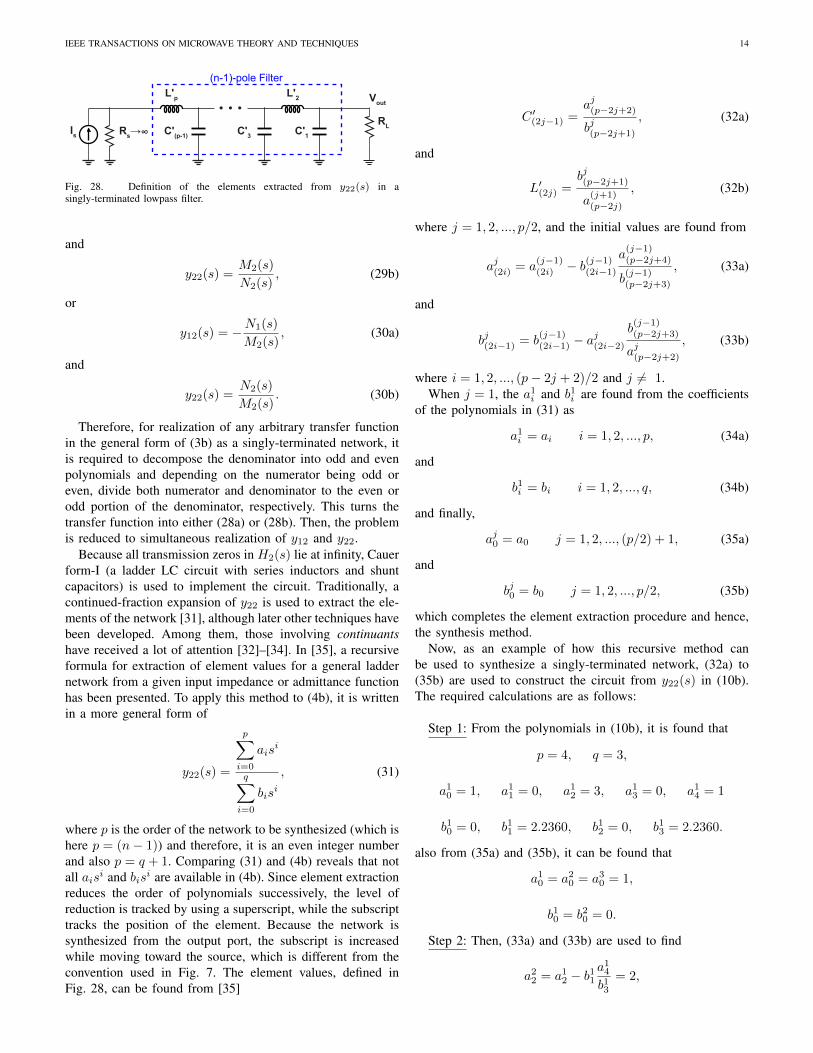
Because all transmission zeros in H2(s) lie at infinity, Cauerform-I (a ladder LC circuit with series inductors and shuntcapacitors) is used to implement the circuit. Traditionally, acontinued-fraction expansion of y22 is used to extract the ele-ments of the network [31], although later other techniques havebeen developed. Among them, those involving continuantshave received a lot of attention [32]–[34]. In [35], a recursiveformula for extraction of element values for a general laddernetwork from a given input impedance or admittance functionhas been presented. To apply this method to (4b), it is writtenin a more general form of
y22(s) =
p∑i=0
aisi
q∑i=0
bisi
, (31)
where p is the order of the network to be synthesized (which ishere p = (n− 1)) and therefore, it is an even integer numberand also p = q + 1. Comparing (31) and (4b) reveals that notall aisi and bisi are available in (4b). Since element extractionreduces the order of polynomials successively, the level ofreduction is tracked by using a superscript, while the subscripttracks the position of the element. Because the network issynthesized from the output port, the subscript is increasedwhile moving toward the source, which is different from theconvention used in Fig. 7. The element values, defined inFig. 28, can be found from [35]
C ′(2j−1) =aj(p−2j+2)
bj(p−2j+1)
, (32a)
and
L′(2j) =bj(p−2j+1)
a(j+1)(p−2j)
, (32b)
where j = 1, 2, ..., p/2, and the initial values are found from
aj(2i) = a(j−1)(2i) − b
(j−1)(2i−1)
a(j−1)(p−2j+4)
b(j−1)(p−2j+3)
, (33a)
and
bj(2i−1) = b(j−1)(2i−1) − a
j(2i−2)
b(j−1)(p−2j+3)
aj(p−2j+2)
, (33b)
where i = 1, 2, ..., (p− 2j + 2)/2 and j 6= 1.When j = 1, the a1
i and b1i are found from the coefficientsof the polynomials in (31) as
a1i = ai i = 1, 2, ..., p, (34a)
and
b1i = bi i = 1, 2, ..., q, (34b)
and finally,
aj0 = a0 j = 1, 2, ..., (p/2) + 1, (35a)
and
bj0 = b0 j = 1, 2, ..., p/2, (35b)
which completes the element extraction procedure and hence,the synthesis method.
Now, as an example of how this recursive method canbe used to synthesize a singly-terminated network, (32a) to(35b) are used to construct the circuit from y22(s) in (10b).The required calculations are as follows:
Step 1: From the polynomials in (10b), it is found that
p = 4, q = 3,
a10 = 1, a1
1 = 0, a12 = 3, a1
3 = 0, a14 = 1
b10 = 0, b11 = 2.2360, b12 = 0, b13 = 2.2360.
also from (35a) and (35b), it can be found that
a10 = a2
0 = a30 = 1,
b10 = b20 = 0.
Step 2: Then, (33a) and (33b) are used to find
a22 = a1
2 − b11a1
4
b13= 2,

IEEE TRANSACTIONS ON MICROWAVE THEORY AND TECHNIQUES 15
b21 = b11 − a20
b13a2
2
= 1.1180.
Step 3: finally, the elements values are found using (32a)and (32b) as
C ′1 = a14/b
13 = 0.4472 F,
L′2 = b13/a22 = 1.1180 H,
C ′3 = a22/b
21 = 1.7889 F,
L′4 = b21/a30 = 1.1180 H.
APPENDIX IINON-LINEAR CIRCUIT ANALYSIS
In this section, a third order Taylor approximation of Voutversus Vin [36], [37] is derived. It is assumed that thesecond order non-linearity is negligible in fully differentialconfiguration.Vout is derived as a function of Vx, V 3
x . From (16)
Vout = −gm2,1
go2︸ ︷︷ ︸a
Vx−gm2,3
go2︸ ︷︷ ︸b
V 3x − V 3
out (36)
Vout = Vout(Vx, V3x ): Vout is defined as: Vout = β1Vx +
β3V3x , which is a 3rd order Taylor approximation around Vx =
0, where β1, β3 are the Taylor coefficients.
βn=1,2,3 =1
n!
(∂nVout∂V nx
) ∣∣∣∣Vx=0
To derive β1, (36) is differentiated with respect to Vx asfollows:
∂Vout∂Vx
= a+ 3bV 2x + 3V 2
out
∂Vout∂Vx
=a+ 3bV 2
x
1− 3V 2out
Taking derivative with respect to Vx again, it is found
∂2Vout∂2Vx
=6bVx + 6Vout
(∂Vout
∂Vx
)2
1− 3V 2out
.
Also, the third derivative gives
∂3Vout∂3Vx
=6b+ 6a3 + 12cVout
(∂Vout
∂Vx
)2
+ 6aVout∂2Vout
∂2Vx
1− 3V 2out
.
Therefore,
β1 =
(∂Vout∂Vx
) ∣∣∣∣Vx=0
= a =−gm2,1
go2,1
β2 =1
2
(∂2Vout∂V 2
x
) ∣∣∣∣Vx=0
= 0
β3 =1
6
(∂3Vout∂V 3
x
) ∣∣∣∣Vx=0
= b+ a3c
As a result, the output voltage
Vout = a︸︷︷︸β1
Vx + (b+ a3)︸ ︷︷ ︸β3
V 3x (37)
Vx = Vx(Vout, V3out): It is possible to write the inverse of
(37) in the Taylor series form: Vx = α1Vout + α3V3out, where
α1, α3 are the Taylor coefficients.
Vx = α1Vout + α3V3out
= α1(β1Vx + β3V3x ) + α3
(β1Vx + β3V
3x
)3= α1β1Vx + α1β3V
3x + α3β1V
3x + ...
Equating the terms on both sides
α1 =1
a
α3 = −b+ a3
a4
Vx =1
a︸︷︷︸α1
Vout −(b+ a3c)
a4︸ ︷︷ ︸α3
V 3out (38)
The output current of first gm cell
Is = −gm1,1Vin − gm1,3V3in (39)
Now, from Fig. 18, it is possible to write
Is = Io + IF =Vxr′o1− gm3,1Vout − gm3,3V
3out
= Vout(−gm3,1 +1
ar′o1)−
(b+ a3c
a4r′o1+ gm3,3
)V 3out
(40)Equating (39) and (40), yeilds
Vout =gm1,1
gm3,1 − 1ar′o1︸ ︷︷ ︸
m
Vin +gm1,3
gm3,3 − 1ar′o1︸ ︷︷ ︸
n
V 3in + pV 3
out
= mVin + nV 3in + pV 3
out
(41)
where p =b+a3c+a4gm3,3r
′o1
a4r′o1
(1
ar′o1−gm3,1
) .Therefore,
∂Vout∂Vin
= m+ 3nV 2in + 3pV 2
out
∂Vout∂Vin
(42)
By using the same procedure above, it is found that
Vout = mVin + (n+m3p)V 3in
=gm1,1
gm3,1 + 1gm2,1r′o1r
′o2
Vin + TV 3in
(43)
where
T =gm1,3
gm3,3 + 1gm2,1ro1ro2
+
(gm1,1
gm3,1 + 1gm2,1ro1ro2
)3
× p.

IEEE TRANSACTIONS ON MICROWAVE THEORY AND TECHNIQUES 16
REFERENCES
[1] “3GPP TS 36.300 v 12.6.0, June 2015; technical specification groupradio access network; evolved universal terrestrial radio access (E-UTRA) and evolved universal terrestrial radio access network (E-UTRAN); overall description; stage 2, release 11.”
[2] R. Chen and H. Hashemi, “Reconfigurable receiver with radio-frequencycurrent-mode complex signal processing supporting carrier aggregation,”IEEE Journal of Solid-State Circuits, vol. 50, no. 12, pp. 3032–3046,Dec. 2015.
[3] Y. Xu and P. R. Kinget, “A switched-capacitor RF front end withembedded programmable high-order filtering,” IEEE Journal of Solid-State Circuits, vol. 51, no. 5, pp. 1154–1167, May 2016.
[4] D. Yang, H. Yuksel, and A. Molnar, “A wideband highly integratedand widely tunable transceiver for in-band full-duplex communication,”IEEE Journal of Solid-State Circuits, vol. 50, no. 5, pp. 1189–1202,May 2015.
[5] M. N. Hasan, Q. J. Gu, and X. Liu, “Tunable blocker-tolerant on-chipradio frequency front-end filter with dual adaptive transmission zeros forsoftware defined radio applications,” IEEE Transactions on MicrowaveTheory and Techniques, vol. 64, no. 12, Dec 2016.
[6] R. Chen and H. Hashemi, “Passive coupled-switched-capacitor-resonator-based reconfigurable RF front-end filters and duplexers,” inProc. IEEE Radio Frequency Integrated Circuits Symp. (RFIC), May2016, pp. 138–141.
[7] N. Reiskarimian and H. Krishnaswamy, “Design of all-passive higher-order cmos n-path filters,” in Radio Frequency Integrated CircuitsSymposium (RFIC), 2015 IEEE. IEEE, 2015, pp. 83–86.
[8] M. Darvishi, R. Van der Zee, and B. Nauta, “Design of active N-pathfilters,” IEEE Journal of Solid-State Circuits, vol. 48, no. 12, pp. 2962–2976, Dec 2013.
[9] C.-K. Luo, P. S. Gudem, and J. F. Buckwalter, “A 0.2–3.6-GHz 10-dBmB1dB 29-dBm IIP3 Tunable filter for transmit leakage suppression inSAW-less 3G/4G FDD receivers,” IEEE Transactions on MicrowaveTheory and Techniques, vol. 63, no. 10, pp. 3514–3524, 2015.
[10] R. Chen and H. Hashemi, “Dual-carrier aggregation receiver withreconfigurable front-end rf signal conditioning,” IEEE Journal of Solid-State Circuits, vol. 50, no. 8, pp. 1874–1888, 2015.
[11] M. N. Hasan, Q. Gu, and X. Liu, “Reconfigurable blocker-tolerant RFfront-end filter with tunable notch for active cancellation of transmitterleakage in FDD receivers,” International Symposium on Circuits andSystems (ISCAS), pp. 1782–1785, May 2016.
[12] A. Ghaffari, E. Klumperink, M. C. M. Soer, and B. Nauta, “Tunablehigh-Q N-path band-pass filters: Modeling and verification,” IEEEJournal of Solid-State Circuits, vol. 46, no. 5, pp. 998–1010, 2011.
[13] A. Ghaffari, E. Klumperink, and B. Nauta, “Tunable N-path notch filtersfor blocker suppression: Modeling and verification,” IEEE Journal ofSolid-State Circuits, vol. 48, no. 6, pp. 1370–1382, 2013.
[14] M. N. Hasan, Q. Gu, and X. Liu, “Tunable blocker-tolerant RF front-endfilter with dual adaptive notches for reconfigurable receivers,” in 2016IEEE MTT-S International Microwave Symposium (IMS), May 2016, pp.1–4.
[15] C. Andrews and A. C. Molnar, “A passive mixer-first receiver withdigitally controlled and widely tunable RF interface,” IEEE Journal ofSolid-State Circuits, vol. 45, no. 12, pp. 2696–2708, Dec. 2010.
[16] C. Andrews and A. C. Molnar, “Implications of passive mixer trans-parency for impedance matching and noise figure in passive mixer-first receivers,” IEEE Transactions on Circuits and Systems I: RegularPapers, vol. 57, no. 12, pp. 3092–3103, Dec. 2010.
[17] R. Chen and H. Hashemi, “Reconfigurable blocker-resilient receiver withconcurrent dual-band carrier aggregation,” in 2014 IEEE Proceedings ofthe Custom Integrated Circuits Conference (CICC), 2014, pp. 1–4.
[18] A. Mirzaei and H. Darabi, “Analysis of imperfections on performanceof 4-phase passive-mixer-based high-q bandpass filters in SAW-lessreceivers,” IEEE Transactions on Circuits and Systems I: RegularPapers, vol. 58, no. 5, pp. 879–892, May 2011.
[19] G. Agrawal, S. Aniruddhan, and R. K. Ganti, “A compact mixer-first receiver with >24 dB self-interference cancellation for full-duplexradios,” IEEE Microwave and Wireless Components Letters, vol. 26,no. 12, pp. 1005–1007, Dec. 2016.
[20] N. Reiskarimian, M. B. Dastjerdi, J. Zhou, and H. Krishnaswamy,“Highly-linear integrated magnetic-free circulator-receiver for full-duplex wireless,” in Proc. IEEE Int. Solid-State Circuits Conf. (ISSCC),Feb. 2017, pp. 316–317.
[21] G. L. Matthaei, L. Young, and E. Jones, Microwave filters, impedance-matching networks, and coupling structures. Dedham, MA, USA:Artech house, 1980.
[22] R. J. Cameron, C. M. Kudsia, and R. R. Mansour, Microwave Filtersfor Communication Systems: Fundamentals, Design and Applications.New York, NY, USA: Wiley-Interscience, 2007.
[23] S. Saeedi, J. Lee, and H. H. Sigmarsson, “A new property of maximally-flat lowpass filter prototype coefficients with application in dissipativeloss calculations,” Progress In Electromagnetics Research C, vol. 63,pp. 1–11, 2016.
[24] D. M. Pozar, Microwave Engineering, 4th Edition. Danvers, MA, USA:John Wiley & Sons, Inc., 2011.
[25] H. Joshi, H. H. Sigmarsson, S. Moon, D. Peroulis, and W. J. Chappell,“High-Q fully reconfigurable tunable bandpass filters,” IEEE transac-tions on microwave theory and techniques, vol. 57, no. 12, pp. 3525–3533, 2009.
[26] E. J. Naglich, J. Lee, D. Peroulis, and W. J. Chappell, “A tunablebandpass-to-bandstop reconfigurable filter with independent bandwidthsand tunable response shape,” IEEE Transactions on Microwave Theoryand Techniques, vol. 58, no. 12, pp. 3770–3779, 2010.
[27] S. Saeedi, J. Lee, and H. H. Sigmarsson, “Tunable, high-Q, substrate-integrated, evanescent-mode cavity bandpass-bandstop filter cascade,”IEEE Microwave and Wireless Components Letters, vol. 26, no. 4, pp.240–242, 2016.
[28] M. Hasan, S. Aggarwal, Q. Gu, and X. Liu, “Tunable N-path RF front-end filter with an adaptive integrated notch for FDD/co-existence,” in2015 IEEE International Midwest Symposium on Circuits and Systems(MWSCAS), 2015, pp. 1–4.
[29] F. Amin, S. Raman, and K. J. Koh, “A high dynamic range 4th-order 4–8 GHz Q-enhanced LC band-pass filter with 2 –25% tunable fractionalbandwidth,” in 2016 IEEE MTT-S International Microwave Symposium(IMS), May 2016, pp. 1–4.
[30] C.-K. Luo, P. S. Gudem, and J. F. Buckwalter, “A 0.4-6-GHz 17–dBmB1dB 36–dBm IIP3 channel-selecting low-noise amplifier for SAW-less 3G/4G FDD diversity receivers,” IEEE Transactions on MicrowaveTheory and Techniques, vol. 64, no. 4, pp. 1110–1121, 2016.
[31] M. E. Van Valkenburg, Introduction to modern network synthesis. NewYork, NY, USA : Wiley, 1965.
[32] H. Orchard, “Some explicit formulas for the components in low-passladder networks,” IEEE Trans. Circuit Theory, vol. 17, no. 4, pp. 612–616, 1970.
[33] P. Mariotto, “On the explicit formulas for the elements in low-pass ladderfilters,” IEEE Trans. Circuits Syst., vol. 37, no. 11, pp. 1429–1436, 1990.
[34] R. Gudipati and W.-K. Chen, “Explicit formulas for element valuesof the lowpass, highpass and bandpass ladders with Butterworth orChebyshev response,” in 1993 IEEE International Midwest Symposiumon Circuits and Systems (MWSCAS), 1993, pp. 645–648.
[35] R. Gudipati and W.-K. Chen, “Explicit formulae for element valuesof a lossless low-pass ladder network and their use in the design ofa broadband matching network,” Journal of the Franklin Institute, vol.326, no. 2, pp. 167–184, 1989.
[36] B. Razavi, RF Microelectronics, 2nd ed. Upper Saddle River, NJ, USA:Prentice Hall Press, 2011.
[37] D. H. Mahrof, E. A. Klumperink, Z. Ru, M. S. Oude Alink, andB. Nauta, “Cancellation of opAmp virtual ground imperfections by anegative conductance applied to improve RF receiver linearity,” IEEEJournal of Solid-State Circuits, vol. 49, no. 5, pp. 1112–1124, 2014.