
IEEE TRANSACTIONS ON MICROWAVE THEORY AND … · zero(1.8GHz).Amaximum32-dBimprovementisattaineddue...
10
IEEE TRANSACTIONS ON MICROWAVE THEORY AND TECHNIQUES, VOL. 58, NO. 2, FEBRUARY 2010 277 Analysis and Design of Two Low-Power Ultra-Wideband CMOS Low-Noise Amplifiers With Out-Band Rejection Ching-Piao Liang, Pei-Zong Rao, Tian-Jian Huang, and Shyh-Jong Chung, Senior Member, IEEE Abstract—Two 3–5-GHz low-power ultra-wideband (UWB) low-noise amplifiers (LNAs) with out-band rejection function using 0.18- m CMOS technology are presented. Due to the Fed- eral Communications Commission’s stringent power-emission limitation at the transmitter, the received signal power in the UWB system is smaller than those of the close narrowband interferers such as the IEEE 802.11 a/b/g wireless local area network, and the 1.8-GHz digital cellular service/global system for mobile com- munications. Therefore, we proposed a wideband input network with out-band rejection capability to suppress the out-band prop- erties for our first UWB LNA. Moreover, a feedback structure and dual-band notch filter with low-power active inductors will further attenuate the out-band interferers without deteriorating the input matching bandwidth in the second UWB LNA. The 55/48/45 dB maximum rejections at 1.8/2.4/5.2 GHz, a power gain of 15 dB, and 3.5-dB minimum noise figure can be measured while consuming a dc power of only 5 mW. Index Terms—Complementary metal–oxide semiconductor (CMOS), low-noise amplifier (LNA), out-band rejection, ultra- wideband (UWB). I. INTRODUCTION U LTRA-WIDEBAND (UWB) systems realize high data rate in the short-range wireless transmission, which are suitable for integration in various consumer electronics such as PCs, cellular phones, digital cameras, and PDAs. The minimum received power in the UWB channel is 47 and 67 dB, in the worst case, lower than those of the wireless local area network (WLAN) interferer powers at 5.2 and 2.4 GHz, respectively [1]. In addition, a tone is measured at 1.87 GHz in a smart phone currently on the market, and the power level is 35 dB higher than the UWB signal [2]. All of these interferers, as shown in Fig. 1, have a harmful effect on the received UWB signal; they can especially lead to the receiver gain compression and their possible intermodulation products can fall in-band. Although the interferers may further be attenuated by the baseband filter in the receiver, this does not address the problems of the intermodula- tion distortion and the receiver gain desensitization. In order to achieve reasonable performance for the above considerations, as summarized in Table I, more than 10-dB attenuation over the bandwidth of each interferer with 20-dB peak attenuation Manuscript received January 13, 2009; revised August 30, 2009. First pub- lished January 15, 2010; current version published February 12, 2010. This work was supported by the National Science Council of Taiwan under Contract NSC96-2752-E009-003-PAE. The authors are with the Department of Communication Engineering, Na- tional Chiao Tung University, Hsinchu 30050, Taiwan (e-mail: sjchung@cm. nctu.edu.tw). Digital Object Identifier 10.1109/TMTT.2009.2037855 Fig. 1. Spectrum of the UWB system with large interferers. TABLE I NOTCH FILTER SPECIFICATIONS is appropriate in the front-end [3]–[7]. On the other hand, a larger attenuation in the front-end can also relax the baseband filter achieving an implementation with the smaller group-delay variations and lower dc power consumption [5]. Recently, a design of multiple-stopband filters is presented for the suppression of interfering signals such as global system for mobile communicatins (GSM), WLAN, and worldwide interop- erability for microwave access (WIMAX) in UWB applications [3]. The coupled resonator stopband filter sections with bent res- onators were adopted in order to more effectively suppress har- monics and the maximum rejection is about 25 dB at 1.8 GHz. However, this prototype of the filter, which was fabricated on the basis of the standard printed circuit board (PCB) process, will increase the entire UWB system area. Moreover, the multiple re- ceivers with equal-gain combining were employed to eliminate the narrowband interferers received in the two paths and com- bined out-of-phase to cancel each other by selecting the optimal local oscillator (LO) phase [4]. A maximum 28-dB attenuation of the interferers was measured, but it is unavoidable to increase the system’s complexity. On the other hand, the topologies utilized for wideband am- plifiers generally include the distributed configuration [8], [9], resistive shunt-feedback structure [10]–[12], common-gate termination [13]–[15], and LC input network [16], [17]. The distributed amplifiers are attractive for their ultra-wide band- width; however, the major drawbacks are the large area and high dc power consumption, which make them unsuitable for many ap- plications. The resistive shunt-feedback and common-gate 0018-9480/$26.00 © 2010 IEEE
Transcript of IEEE TRANSACTIONS ON MICROWAVE THEORY AND … · zero(1.8GHz).Amaximum32-dBimprovementisattaineddue...

IEEE TRANSACTIONS ON MICROWAVE THEORY AND TECHNIQUES, VOL. 58, NO. 2, FEBRUARY 2010 277
Analysis and Design of Two Low-PowerUltra-Wideband CMOS Low-NoiseAmplifiers With Out-Band Rejection
Ching-Piao Liang, Pei-Zong Rao, Tian-Jian Huang, and Shyh-Jong Chung, Senior Member, IEEE
Abstract—Two 3–5-GHz low-power ultra-wideband (UWB)low-noise amplifiers (LNAs) with out-band rejection functionusing 0.18- m CMOS technology are presented. Due to the Fed-eral Communications Commission’s stringent power-emissionlimitation at the transmitter, the received signal power in the UWBsystem is smaller than those of the close narrowband interfererssuch as the IEEE 802.11 a/b/g wireless local area network, andthe 1.8-GHz digital cellular service/global system for mobile com-munications. Therefore, we proposed a wideband input networkwith out-band rejection capability to suppress the out-band prop-erties for our first UWB LNA. Moreover, a feedback structureand dual-band notch filter with low-power active inductors willfurther attenuate the out-band interferers without deterioratingthe input matching bandwidth in the second UWB LNA. The55/48/45 dB maximum rejections at 1.8/2.4/5.2 GHz, a power gainof 15 dB, and 3.5-dB minimum noise figure can be measured whileconsuming a dc power of only 5 mW.
Index Terms—Complementary metal–oxide semiconductor(CMOS), low-noise amplifier (LNA), out-band rejection, ultra-wideband (UWB).
I. INTRODUCTION
U LTRA-WIDEBAND (UWB) systems realize high datarate in the short-range wireless transmission, which are
suitable for integration in various consumer electronics such asPCs, cellular phones, digital cameras, and PDAs. The minimumreceived power in the UWB channel is 47 and 67 dB, in theworst case, lower than those of the wireless local area network(WLAN) interferer powers at 5.2 and 2.4 GHz, respectively [1].In addition, a tone is measured at 1.87 GHz in a smart phonecurrently on the market, and the power level is 35 dB higherthan the UWB signal [2]. All of these interferers, as shown inFig. 1, have a harmful effect on the received UWB signal; theycan especially lead to the receiver gain compression and theirpossible intermodulation products can fall in-band. Although theinterferers may further be attenuated by the baseband filter in thereceiver, this does not address the problems of the intermodula-tion distortion and the receiver gain desensitization. In order toachieve reasonable performance for the above considerations,as summarized in Table I, more than 10-dB attenuation overthe bandwidth of each interferer with 20-dB peak attenuation
Manuscript received January 13, 2009; revised August 30, 2009. First pub-lished January 15, 2010; current version published February 12, 2010. Thiswork was supported by the National Science Council of Taiwan under ContractNSC96-2752-E009-003-PAE.
The authors are with the Department of Communication Engineering, Na-tional Chiao Tung University, Hsinchu 30050, Taiwan (e-mail: [email protected]).
Digital Object Identifier 10.1109/TMTT.2009.2037855
Fig. 1. Spectrum of the UWB system with large interferers.
TABLE INOTCH FILTER SPECIFICATIONS
is appropriate in the front-end [3]–[7]. On the other hand, alarger attenuation in the front-end can also relax the basebandfilter achieving an implementation with the smaller group-delayvariations and lower dc power consumption [5].
Recently, a design of multiple-stopband filters is presented forthe suppression of interfering signals such as global system formobile communicatins (GSM), WLAN, and worldwide interop-erability for microwave access (WIMAX) in UWB applications[3]. The coupled resonator stopband filter sections with bent res-onators were adopted in order to more effectively suppress har-monics and the maximum rejection is about 25 dB at 1.8 GHz.However, this prototype of the filter, which was fabricated on thebasis of the standard printed circuit board (PCB) process, willincrease the entire UWB system area. Moreover, the multiple re-ceivers with equal-gain combining were employed to eliminatethe narrowband interferers received in the two paths and com-bined out-of-phase to cancel each other by selecting the optimallocal oscillator (LO) phase [4]. A maximum 28-dB attenuationof the interferers was measured, but it is unavoidable to increasethe system’s complexity.
On the other hand, the topologies utilized for wideband am-plifiers generally include the distributed configuration [8], [9],resistive shunt-feedback structure [10]–[12], common-gate
termination [13]–[15], and LC input network [16], [17].The distributed amplifiers are attractive for their ultra-wide band-width; however, the major drawbacks are the large area and highdcpowerconsumption,whichmake themunsuitable formanyap-plications. The resistive shunt-feedback and common-gate
0018-9480/$26.00 © 2010 IEEE

278 IEEE TRANSACTIONS ON MICROWAVE THEORY AND TECHNIQUES, VOL. 58, NO. 2, FEBRUARY 2010
amplifiers can provide good impedance matching and moderategain while dissipating small amounts of dc power, but withoutthe out-band rejection capability. Recently, a new topology ofthe broadband amplifier for out-band rejection, which adopted anotch filter circuit with negative-resistance cell embedded, hasbeen reported in [18] and [19]. Inevitably, the extra notch filtercircuit made of inductors and cross-coupled transistors willoccupy additional chip area and dc power simultaneously.
In this paper, we propose two topologies of the 3–5-GHzUWB low-noise amplifier (LNA) with out-of-band suppressionby using the CMOS technology. In the first UWB LNA, a newwideband input impedance-matching network, which is based onthe LC structure with focus on the improvement of out-of-bandrejection capability, is presented. By suitably introducing twoadditional capacitors in the traditional LC input network, twotransmission zeros at 1.8 and 8.5 GHz are generated to achievethe out-band rejection property without suffering from dete-rioration of the in-band performance. As an improvement ofthe first approach, the second proposed UWB LNA introducesa capacitive feedback path to the input LC network for furtherenhancing the rejection capability at the lower band transmissionzero (1.8 GHz). A maximum 32-dB improvement is attained dueto the usage of a feedback capacitor. A dual-band notch filtermade of active inductors, which occupies only a small chip area,is also employed after the LNA core so as to attenuate the WLANinterferers at 2.4 and 5.2 GHz without influencing the noise figure(NF) of the LNA. The proposed active inductors are designedbased on the cascode gain-boosting stage with a feedback re-sistor, which are with low consumption power while maintaininga sufficient value. The introducing of both the feedback capac-itor and the dual-band notch filter achieves maximum rejectionsof about 50 dB on the out-band interferers, which is superior tothose presented in the literature [3], [4], [18], [19]. This paper isorganized as follows. Sections II and III present the analyses ofthe first and second UWB LNAs, respectively. The circuit imple-mentation and experimental results are illustrated in Section IV,followed by a conclusion in Section V. In this study, the circuitsimulation is performed via Agilent’s Advanced Design System(ADS) software with a TSMC design kit.
II. FIRST UWB LNA
The first 3–5-GHz CMOS UWB LNA proposed here adoptsa source-degenerated cascode configuration, as shown in Fig. 2.An LC input network for wideband operation is utilized withtwo new capacitors and for increasing the higher andlower out-band rejections, respectively. The load inductorin series with the resistor helps to enhance the gain flatness.The buffer transistor with a purely resistive load is em-ployed for testing purposes.
A. Power Gain
The overall gain of the proposed LNA can be easily obtainedas follows after a straightforward derivation:
(1)
Fig. 2. Complete schematics of the first UWB LNA with out-band rejection.
where
(2)with
(3)
is the 50- source resistance, , and isthe total capacitance between the drain of the transistor andground. is the reflection coefficient at the input port. From(1), it is seen that extra transmission zeros (i.e., ) can becreated when the following conditions are satisfied:
or (4)
in which means that the input impedance of the LNAis short circuit, and it occurs as the impedance , i.e., theimpedance of the tank in series with the capacitor(see Fig. 2) is equal to zero, where
(5)
By using (2), (4), and (5), the locations of transmission zeroscan be predicted as
(6)
B. Optimum Out-Band Rejection
The above ratiocination reveals that the additional capaci-tors and will bring about two transmission zeros toameliorate the out-band performance. However, the out-bandrejection characteristics are restricted by the series resistanceof the on-chip inductor. As seen from(6), the higher and lowerout-band transmission zeros are associated with the inductors
and , respectively. These component values influence not

LIANG et al.: ANALYSIS AND DESIGN OF TWO LOW-POWER UWB CMOS LNAs 279
Fig. 3. (a) Simulated power gain �� � and (b) input return loss ���� � fordifferent values of� with� � ��� nH,� � ���� pF, and� � ��� pF.The transmission zero � is kept constant.
only the zeros’ frequencies, but also the out-band suppressionlevels, as shown below.
Fig. 3(a) shows the power gain versus frequency withdifferent values of . To begin with, it can be anticipated that thehigher frequencyout-bandeliminationefficiency is mainly deter-mined by the impedance of the tank at the resonant fre-quency (i.e., the larger impedance, thesuperiorout-bandsuppres-sion). Therefore, the first step is to assign a larger to arrive atlarger resonant impedance [20, Ch. 14]. In addition, a preferablepower gain in the target frequency range can be procured contem-poraneously by using a larger , as shown in Fig. 3(a). However,an overlarge will lead to over abounded input impedance,as shown in Fig. 3(b), thus decreasing the input matching band-width of the LNA, which is not desirable for this design.
As is clear from (5), the impedance in Fig. 2 producesone series and one parallel resonance from which the lowertransmission zero can be created. It is expectable that a smallerimpedance at the series resonant frequency will accomplishthe superior out-band elimination efficiency. Fig. 4 shows the re-lation between the impedance and frequency for differentvalues. As is seen, a smaller results in a smaller . This, inturn, does cause a deeper suppression level at (1.8 GHz), ascan be observed from the power gain versus frequency diagramshown in Fig. 5(a). Nevertheless, a drawback that may makethe design unsatisfactory is that a diminishing , and thus, adeceasing , may reduce the input impedance, and thus, dete-riorate the matching condition, as demonstrated in Fig. 5(b).
Fig. 4. Impedance� versus frequency with different values of� . The trans-mission zero � is kept constant.
Fig. 5. (a) Simulated power gain �� � and (b) input return loss ���� � fordifferent values of � with � � ��� nH, � � �� nH, � � ��� pF, and� � ���� pF. The transmission zero � is kept constant.
From the above discussion, it should be taken into accountpunctiliously by choosing appropriate values of and toachieve the tradeoff between the input match and out-band re-jection performances.
It is interesting to see the influence of the input network onthe LNA’s NF. After a straightforward derivation following theprocedure in [21], the NF of the circuit shown in Fig. 2 can beobtained as
(7)
280 IEEE TRANSACTIONS ON MICROWAVE THEORY AND TECHNIQUES, VOL. 58, NO. 2, FEBRUARY 2010
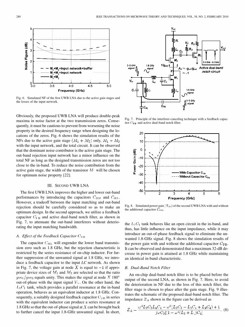
Fig. 6. Simulated NF of the first UWB LNA due to the active gain stages andthe losses of the input network.
Obviously, the proposed UWB LNA will produce double-peakmaxima in noise factor at the two transmission zeros. Conse-quently, it must be cautious to prevent from worsening the noiseproperty in the desired frequency range when designing the lo-cations of the zeros. Fig. 6 shows the simulation results of theNFs due to the active gain stage only,with the input network, and the total circuit. It can be observedthat the dominant noise contributor is the active gain stage. Theout-band rejection input network has a minor influence on thetotal NF as long as the designed transmission zeros are not tooclose to the in-band. To reduce the noise contribution from theactive gain stage, the width of the transistor will be chosenfor optimum noise property [22].
III. SECOND UWB LNA
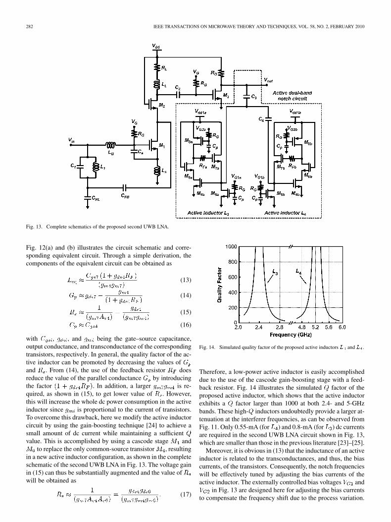
The first UWB LNA improves the higher and lower out-bandperformances by introducing the capacitors and .However, a tradeoff between the input matching and out-bandrejection should be carefully considered so as to make anoptimum design. In the second approach, we utilize a feedbackcapacitor and active dual-band notch filter, as shown inFig. 7, to attenuate the out-band interferers without deterio-rating the input matching bandwidth.
A. Effect of the Feedback Capacitor
The capacitor will engender the lower band transmis-sion zero such as 1.8 GHz, but the rejection characteristic isrestricted by the series resistance of on-chip inductor. For fur-ther suppression of the unwanted signal at 1.8 GHz, we intro-duce a feedback capacitor to the input LC network. As shownin Fig. 7, the voltage gain at node is equal to if appro-priate device sizes of and are selected so that the ratio
equals unity. This makes the signal at node 180out-of-phase with the input signal . On the other hand, the
tank, which provides a parallel resonance at the in-bandoperation, behaves as an equivalent inductor at 1.8 GHz. Con-sequently, a suitably designed feedback capacitor in serieswith the equivalent inductor can produce a series resonance at1.8 GHz so that the out-of-phase signal at can be brought backto further cancel the input 1.8-GHz unwanted signal. In short,
Fig. 7. Principle of the interferer-canceling technique with a feedback capac-itor � and active dual-band notch filter.
Fig. 8. Simulated power gain �� � of the second UWB LNA with and withoutthe additional capacitor � .
the tank behaves like an open circuit in the in-band, andthus, has little influence on the input impedance, while it mayintroduce an out-of-phase feedback signal to eliminate the un-wanted 1.8-GHz signal. Fig. 8 shows the simulation results ofthe power gain with and without the additional capacitor .It can be observed and demonstrated that a maximum 32-dB de-crease in power gain is attained at 1.8 GHz while maintainingan identical in-band characteristic.
B. Dual-Band Notch Filter
An on-chip dual-band notch filter is to be placed before theoutput of the second LNA, as shown in Fig. 7. Here, to avoidthe deterioration in NF due to the loss of this notch filter, thefilter stage is chosen to place after the gain stage. Fig. 9 illus-trates the schematic of the proposed dual-band notch filter. Theimpedance shown in the figure can be derived as
(8)

LIANG et al.: ANALYSIS AND DESIGN OF TWO LOW-POWER UWB CMOS LNAs 281
Fig. 9. Dual-band notch filter circuit.
Fig. 10. Simulated transmission coefficient � of the notch filter for differentvalues of � .
The notch frequencies of the filter can be obtained by letting thenumerator equal null or
(9)
which results in two transmission zeros and satisfying
(10)
(11)
Also, from (8), the impedance contains a pole at
(12)
In this study, we contrive that , , and correspondto 2.4, 5.2, and 3.9 GHz, respectively. We will determine the ap-propriate values of , , , and for the dual-band notchfilter circuit in order to attenuate the WLAN interferers. It isnoted that, after the decision of the positions of zeros and pole,we get three equations, i.e., (10)–(12), for the four filter compo-nents, which means that there is still one degree of freedom, letus say , left for the circuit design. Fig. 10 shows the transmis-sion coefficients of the notch filter with different values.As the value of increases, the in-band performance from 3.1to 4.8 GHz will be improved; this means that we may use a largerinductance to maintain a better property in the target frequency
Fig. 11. Simulated transmission coefficient � of the notch filter for differentvalues of � with � � � nH.
Fig. 12. (a) Schematic and (b) equivalent circuit of the active inductor with aresistor in the feedback path.
range. To achieve a 10-dB attenuation in both 2.4- and 5.2-GHzbands without suffering from deterioration of the in-band per-formance, the value of nH in the proposed notch filterwill be chosen. On the other hand, the quality factor of theinductor also influences the performance of the filter, as can beobserved from Fig. 11, where the transmission coefficients ofthe filter for different inductor values are shown. It is seen thata low quality factor will deteriorate the maximum attenuation ofthe notch filter. To obtain a 20-dB attenuation of the notch filterfor the required specifications, the value of the quality factormust be higher than 100. In general, the negative-resistance cellby using cross-coupled transistors can be employed to amelio-rate the value of the on-chip inductor. However, the larger in-ductors with cross-coupled transistors will concurrently occupyan overlarge chip area and dc power. Therefore, we are inclinedto utilize active circuitry to substitute for the integrated passiveinductors.
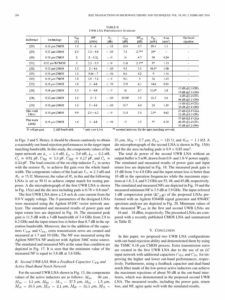
C. Low-Power Active Inductors
The realization of inductances and is based on theactive inductor with a feedback resistor proposed in [23].
282 IEEE TRANSACTIONS ON MICROWAVE THEORY AND TECHNIQUES, VOL. 58, NO. 2, FEBRUARY 2010
Fig. 13. Complete schematics of the proposed second UWB LNA.
Fig. 12(a) and (b) illustrates the circuit schematic and corre-sponding equivalent circuit. Through a simple derivation, thecomponents of the equivalent circuit can be obtained as
(13)
(14)
(15)
(16)
with , , and being the gate–source capacitance,output conductance, and transconductance of the correspondingtransistors, respectively. In general, the quality factor of the ac-tive inductor can be promoted by decreasing the values ofand . From (14), the use of the feedback resistor doesreduce the value of the parallel conductance by introducingthe factor . In addition, a larger is re-quired, as shown in (15), to get lower value of . However,this will increase the whole dc power consumption in the activeinductor since is proportional to the current of transistors.To overcome this drawback, here we modify the active inductorcircuit by using the gain-boosting technique [24] to achieve asmall amount of dc current while maintaining a sufficientvalue. This is accomplished by using a cascode stage and
to replace the only common-source transistor , resultingin a new active inductor configuration, as shown in the completeschematic of the second UWB LNA in Fig. 13. The voltage gainin (15) can thus be substantially augmented and the value ofwill be obtained as
(17)
Fig. 14. Simulated quality factor of the proposed active inductors � and � .
Therefore, a low-power active inductor is easily accomplisheddue to the use of the cascode gain-boosting stage with a feed-back resistor. Fig. 14 illustrates the simulated factor of theproposed active inductor, which shows that the active inductorexhibits a factor larger than 1000 at both 2.4- and 5-GHzbands. These high- inductors undoubtedly provide a larger at-tenuation at the interferer frequencies, as can be observed fromFig. 11. Only 0.55-mA (for ) and 0.8-mA (for ) dc currentsare required in the second UWB LNA circuit shown in Fig. 13,which are smaller than those in the previous literature [23]–[25].
Moreover, it is obvious in (13) that the inductance of an activeinductor is related to the transconductances, and thus, the biascurrents, of the transistors. Consequently, the notch frequencieswill be effectively tuned by adjusting the bias currents of theactive inductor. The externally controlled bias voltages and
in Fig. 13 are designed here for adjusting the bias currentsto compensate the frequency shift due to the process variation.

LIANG et al.: ANALYSIS AND DESIGN OF TWO LOW-POWER UWB CMOS LNAs 283
Fig. 15. Microphotograph of: (a) the first UWB LNA with 0.78�0.8 mm diearea and (b) the second UWB LNA with 0.9� 0.85 mm die area.
Fig. 16. Measured and simulated power gain �� � and input return loss���� � of the first UWB LNA.
Fig. 17. Measured and simulated NF of the first UWB LNA.
For further design, these control voltages and can beutilized together with a feedback mechanism demonstrated in[6] and [7] and [26] and [27] for automatically calibrating thefrequency drift of the notch filters.
IV. IMPLEMENTATION AND MEASUREMENTS
The proposed out-band rejection UWB LNAs are designedand fabricated using the TSMC 0.18- m CMOS process. More-over, on-wafer probing is performed to measure the character-istics of the LNA circuits.
Fig. 18. Measured and simulated power gain �� � and input return loss���� � of the second UWB LNA.
Fig. 19. Measured and simulated NF of the second UWB LNA.
Fig. 20. Measured �� of the proposed UWB LNAs.
A. First UWB LNA With Capacitors and
For the first UWB LNA shown in Fig. 2, the width of thetransistor m is optimized with 2.5-mW power dissi-pation to achieve good noise property. The size of the cascodetransistor m is selected to be as large as possible toreduce its voltage headroom requirement, which is conduciveto low-voltage operations. In addition, the design of the inputnetwork will engender the tradeoff between the input matchand out-band rejection characteristics, which can be observed
284 IEEE TRANSACTIONS ON MICROWAVE THEORY AND TECHNIQUES, VOL. 58, NO. 2, FEBRUARY 2010
TABLE IIUWB LNA PERFORMANCE SUMMARY
in Figs. 3 and 5. Hence, it should be chosen cautiously to obtaina reasonably out-band rejection performances in the target inputmatching bandwidth. In this study, the components values of theinput network are nH, nH, nH,
pF, pF, pF, andpF . The load consists of the on-chip inductor in series
with the resistor to achieve flat gain over the whole band-width. The components values of the load are nH and
. Moreover, the value of in this and the followingLNAs is set as 50 to achieve output match for testing pur-poses. A die microphotograph of the first UWB LNA is shownin Fig. 15(a) and the die area including pads is 0.78 0.8 mm .
The first UWB LNA drew a 2.8-mA dc core current from the0.9-V supply voltage. The -parameters of the designed LNAswere measured using the Agilent 8510C vector network ana-lyzer. The simulated and measured results of power gain andinput return loss are depicted in Fig. 16. The measured peakgain is 11.5 dB with a 3-dB bandwidth of 3.4 GHz from 2.8 to6.2 GHz and the input return loss is better than 8.7 dB in the op-eration bandwidth. Moreover, due to the addition of the capac-itors and , extra transmission zeros are created andmeasured at 1.7 and 10 GHz. The NF was measured using theAgilent N8975A NF analyzer with Agilent 346C noise source.The simulated and measured NFs at the same bias condition aredepicted in Fig. 17. It is seen that the minimum value of themeasured NF is equal to 3.8 dB at 3.6 GHz.
B. Second UWB LNA With a Feedback Capacitor andActive Dual-Band Notch Network
For the second UWB LNA shown in Fig. 13, the componentsvalues of the active inductors are as follows: m ,
m, m, m,m, m, m,
m, m, , and k . Adie microphotograph of the second LNA is shown in Fig. 15(b)and the die area including pads is 0.9 0.85 mm .
The total dc power of the second UWB LNA without anoutput buffer is 5 mW, drawn from 0.9- and 1.8-V power supply.The simulated and measured results of power gain and inputreturn loss are depicted in Fig. 18. The measured peak gain is15 dB from 3 to 4.8 GHz and the input return loss is better than10 dB in the operation frequencies while the maximum rejec-tions at 1.8, 2.4, and 5.2 GHz are 55, 48, and 45 dB, respectively.The simulated and measured NFs are depicted in Fig. 19 and themeasured minimum NF is 3.5 dB at 3.9 GHz. The input-referred1-dB compression point ( ) of the proposed LNAs per-formed with an Agilent 83640B signal generator and 8564ECspectrum analyzer are depicted in Fig. 20. Minimum values ofthe measured in the first and second UWB LNAs are
16 and 18 dBm, respectively. The presented LNAs are com-pared with a recently published CMOS LNA and summarizedin Table II.
V. CONCLUSION
In this paper, we proposed two UWB LNA configurationswith out-band rejection ability and demonstrated them by usingthe TSMC 0.18- m CMOS process. Extra transmission zerosare created in the first UWB LNA due to the use of an LCinput network with additional capacitors and for im-proving the higher and lower out-band performances, respec-tively. Furthermore, using a feedback capacitor and dual-bandnotch filter made of the low-power active inductors can achievethe maximum rejections of about 50 dB at the out-band inter-ferers, which was demonstrated in the proposed second UWBLNA. The measured results, including the power gain, returnloss, and NF, agree quite well with the simulated results.

LIANG et al.: ANALYSIS AND DESIGN OF TWO LOW-POWER UWB CMOS LNAs 285
ACKNOWLEDGMENT
The authors would like to thank the National Chip Implemen-tation Center (CIC), Taiwan, for the help of chip fabrication.
REFERENCES
[1] S. Lo, I. Sever, S.-P. Ma, P. Jang, A. Zou, C. Arnott, K. Ghatak, A.Schwartz, L. Huynh, V. T. Phan, and T. Nguyen, “A dual-antennaphased-array UWB transceiver in 0.18-�m CMOS,” IEEE J. Solid-State Circuits, vol. 41, no. 12, pp. 2776–2786, Dec. 2006.
[2] T. W. Fischer, B. Kelleci, K. Shi, A. I. Karsilayan, and E. Serpedin,“An analog approach to suppressing in-band narrow-band interferencein UWB receivers,” IEEE Trans. Circuits Syst. I, Reg. Papers, vol. 54,no. 5, pp. 941–950, May 2007.
[3] K. Rambabu, M. Y.-W. Chia, K. M. Chan, and J. Bornemann, “De-sign of multiple-stopband filters for interference suppression in UWBapplications,” IEEE Trans. Microw. Theory Tech., vol. 54, no. 8, pp.3333–3338, Aug. 2006.
[4] I. Sever, S. Lo, S.-P. Ma, P. Jang, A. Zou, C. Arnott, K. Ghatak, A.Schwartz, L. Huynh, and T. Nguyen, “A dual-antenna phase-arrayultra-wideband CMOS transceiver,” IEEE Commun. Mag., vol. 44, no.8, pp. 102–110, Aug. 2006.
[5] A. Valdes-Garcia, C. Mishra, F. Bahmani, J. Silva-Martinez, and E.Sánchez-Sinencio, “An 11-band 3–10 GHz receiver in SiGe BiCMOSfor multiband OFDM UWB communication,” IEEE J. Solid-State Cir-cuits, vol. 42, no. 4, pp. 935–948, Apr. 2007.
[6] A. Bevilacqua, A. Maniero, A. Gerosa, and A. Neviani, “An integratedsolution for suppressing WLAN signals in UWB receivers,” IEEETrans. Circuits Syst. I, Reg. Papers, vol. 54, no. 8, pp. 1617–1625,Aug. 2007.
[7] A. Vallese, A. Bevilacqua, C. Sandner, M. Tiebout, A. Gerosa, and A.Neviani, “Analysis and design of an integrated notch filter for the re-jection of interference in UWB systems,” IEEE J. Solid-State Circuits,vol. 44, no. 2, pp. 331–343, Feb. 2009.
[8] X. Guan and C. Nguyen, “Low-power-consumption and high-gainCMOS distributed amplifiers using cascade of inductively coupledcommon-source gain cells for UWB systems,” IEEE Trans. Microw.Theory Tech., vol. 54, no. 8, pp. 3278–3283, Aug. 2006.
[9] P. Heydari, “Design and analysis of a performance-optimized CMOSUWB distributed LNA,” IEEE J. Solid-State Circuits, vol. 42, no. 9,pp. 1892–1905, Sep. 2007.
[10] Y. Park, C.-H. Lee, J. D. Cressler, and J. Laskar, “The analysis of UWBSiGe HBT LNA for its noise, linearity, and minimum group delay varia-tion,” IEEE Trans. Microw. Theory Tech., vol. 54, no. 4, pp. 1687–1697,Apr. 2006.
[11] P. Z. Rao, Y. C. Cheng, C. P. Liang, and S. J. Chung, “Cascode feed-back amplifier combined with resonant matching for UWB system,” inProc. Progr. Electromagn. Res. Symp., Mar. 2007, pp. 1040–1043.
[12] J. Lee and J. D. Cressler, “Analysis and design of an ultra-widebandlow-noise amplifier using resistive feedback in SiGe HBT technology,”IEEE Trans. Microw. Theory Tech., vol. 54, no. 3, pp. 1262–1268, Mar.2006.
[13] G. Cusmai, M. Brandolini, P. Rossi, and F. Svelto, “A 0.18-�m CMOSselective receiver front-end for UWB applications,” IEEE J. Solid-StateCircuits, vol. 41, no. 8, pp. 1764–1771, Aug. 2006.
[14] Y. Lu, K. S. Yeo, A. Cabuk, J. Ma, M. A. Do, and Z. Lu, “A novelCMOS low-noise amplifier design for 3.1- to 10.6-GHz ultra-wide-band wireless receivers,” IEEE Trans. Circuits Syst. I, Reg. Papers, vol.53, no. 8, pp. 1683–1692, Aug. 2006.
[15] X. Li, S. Shekhar, and D. J. Allstot, “��-boosted common-gate LNAand differential Colpitts VCO/QVCO in 0.18-�m CMOS,” IEEE J.Solid-State Circuits, vol. 40, no. 12, pp. 2609–2619, Dec. 2005.
[16] A. Bevilacqua and A. M. Niknejad, “An ultrawideband CMOS low-noise amplifier for 3.1–10.6-GHz wireless receivers,” IEEE J. Solid-State Circuits, vol. 39, no. 12, pp. 2259–2268, Dec. 2004.
[17] A. Ismail and A. A. Abidi, “A 3–10-GHz low-noise amplifier withwideband LC-ladder matching network,” IEEE J. Solid-State Circuits,vol. 39, no. 12, pp. 2269–2277, Dec. 2004.
[18] A. Bevilacqua, A. Vallese, C. Sandner, M. Tiebout, A. Gerosa, and A.Neviani, “A 0.13-�m CMOS LNA with integrated balun and notchfilter for 3 to 5 GHz UWB receivers,” in IEEE Int. Solid-State CircuitsConf. Tech. Dig., Feb. 2007, pp. 420–421.
[19] Y. Gao, Y. J. Zheng, and B. L. Ooi, “0.18-�m CMOS dual-band UWBLNA with interference rejection,” Electron. Lett., vol. 43, no. 20, pp.1096–1098, Sep. 2007.
[20] B. Razavi, Design of Analog CMOS Integrated Circuits. New York:McGraw-Hill, 2000.
[21] D. K. Shaeffer and T. H. Lee, “A 1.5-V, 1.5-GHz CMOS low noiseamplifier,” IEEE J. Solid-State Circuits, vol. 32, no. 5, pp. 745–759,May 1997.
[22] K.-J. Sun, Z.-M. Tsai, K.-Y. Lin, and H. Wang, “A noise optimizationformulation for CMOS low-noise amplifiers with on-chip low-�inductors,” IEEE Trans. Microw. Theory Tech., vol. 54, no. 4, pp.1554–1560, Apr. 2006.
[23] M.-J. Wu, J.-N. Yang, and C.-Y. Lee, “A constant power consumptionCMOS LC oscillator using improved high-� active inductor with widetuning-range,” in Proc. IEEE 47th Midwest Circuits Syst. Symp., Jul.2004, vol. 3, pp. 347–350.
[24] U. Yodprasit and J. Ngarmnil, “�-enhancing technique for RF CMOSactive inductor,” in Proc. IEEE Int. Symp. Circuits Syst., May 2000, pp.589–592.
[25] H.-H. Hsieh, Y.-T. Liao, and L.-H. Lu, “A compact quadrature hybridMMIC using CMOS active inductors,” IEEE Trans. Microw. TheoryTech., vol. 55, no. 6, pp. 1098–1104, Jun. 2007.
[26] T. Das, A. G. C. Washburn, and P. R. Mukund, “Self-calibration ofinput-match in R.F. front-end circuitry,” IEEE Trans. Circuits Syst. II,Exp. Briefs, vol. 52, no. 12, pp. 821–825, Dec. 2005.
[27] A. Vallese, A. Bevilacqua, C. Sandner, M. Tiebout, A. Gerosa, and A.Neviani, “An analog front-end with integrated notch filter for 3–5 GHzUWB receivers in 0.13 �m CMOS,” in Proc. IEEE Eur. Solid-StateCircuits Conf., Munich, Germany, Sep. 2007, pp. 139–142.
[28] C.-P. Chang and H.-R. Chuang, “0.18-�m 3–6 GHz CMOS broad-bandLNA for UWB radio,” Electron. Lett., vol. 41, no. 12, pp. 696–698, Jun.2005.
[29] J. Lerdworatawee and W. Namgoong, “Wide-band CMOS cascode lownoise amplifier design based on source degeneration topology,” IEEETrans. Circuits Syst. I, Reg. Papers, vol. 52, no. 11, pp. 2327–2334,Nov. 2005.
[30] R. Gharpurey, “A broad-band low noise front-end amplifier for ultra-wideband in 0.13 �m,” IEEE J. Solid-State Circuits, vol. 40, no. 9, pp.1983–1986, Sep. 2005.
[31] M. Liu, J. Craninckx, N. M. Iyer, M. Kuijk, and A. R. F. Barel, “A 6.5kV ESD-protected 3–5-GHz ultra-wideband BiCMOS low noise am-plifier using interstage gain roll-off compensation,” IEEE Trans. Mi-crow. Theory Tech., vol. 54, no. 4, pp. 1698–1706, Apr. 2006.
[32] A. Bevilacqua, C. Sandner, A. Gerosa, and A. Neviani, “A fully inte-grated differential CMOS LNA for 3–5 GHz ultra-wideband wirelessreceivers,” IEEE Microw. Wireless Compon. Lett., vol. 16, no. 3, pp.134–136, Mar. 2006.
[33] F. Zhang and P. R. Kinget, “Low-power programmable gain CMOSdistributed LNA,” IEEE J. Solid-State Circuits, vol. 41, no. 6, pp.1333–1343, Jun. 2006.
[34] Y.-J. E. Chen and Y.-I. Huan, “Development of integrated broad-bandCMOS low noise amplifiers,” IEEE Trans. Circuits Syst. I, Reg. Papers,vol. 54, no. 10, pp. 2120–2127, Oct. 2007.
[35] M. l. Jeong, J. N. Lee, and C. S. Lee, “Design of UWB switched gaincontrolled LNA using 0.18-�m CMOS,” Electron. Lett., vol. 44, no. 7,pp. 477–478, Mar. 2008.
[36] S.-K. Tang, K.-P. Pun, C.-S. Choy, C.-F. Chan, and K. N. Leung, “Afully differential band-selective low-noise amplifier for MB-OFDMUWB receivers,” IEEE Trans. Circuits Syst. II, Exp. Briefs, vol. 55,no. 7, pp. 653–657, Jul. 2008.
Ching-Piao Liang was born in Changhwa, Taiwan,in 1980. He received the B.S. and M.S. degreesin communication engineering from Yuan ZeUniversity, Taoyuan, Taiwan, in 2003 and 2005,respectively, and is currently working toward thePh.D. degree in communication engineering fromNational Chiao Tung University, Hsinchu, Taiwan.
His primary research interests include RF inte-grated circuits and monolithic microwave integratedcircuits.

286 IEEE TRANSACTIONS ON MICROWAVE THEORY AND TECHNIQUES, VOL. 58, NO. 2, FEBRUARY 2010
Pei-Zong Rao was born in Kaohsiung, Taiwan, in1980. He received the B.S. degree in physics fromNational Kaohsiung Normal University, Kaohsiung,Taiwan, in 2002, and is currently working toward thePh.D. degree in communication engineering fromNational Chiao Tung University, Hsinchu, Taiwan.
His research interests include RF integratedcircuits, multiband wireless systems, and frequencysynthesizer designs.
Tian-Jian Huang was born in Taichung, Taiwan, in1983. He received the B.S. and M.S. degrees in com-munication engineering from National Chiao TungUniversity, Hsinchu, Taiwan, in 2006 and 2008, re-spectively.
His research focuses on RF integrated circuit de-sign.
Shyh-Jong Chung (M’92–SM’06) was born inTaipei, Taiwan. He received the B.S.E.E. and Ph.D.degrees from National Taiwan University, Taipei,Taiwan, in 1984 and 1988, respectively.
Since 1988, he has been with the Department ofCommunication Engineering, National Chiao TungUniversity, Hsinchu, Taiwan, where he is currently aProfessor and serves as the Director of the Institute ofCommunication Engineering. From September 1995to August 1996, he was a Visiting Scholar with theDepartment of Electrical Engineering, Texas, A&M
University, College Station. His areas of interest include the design and appli-cations of active and passive planar antennas, low-temperature co-fired ceramic(LTCC)-based RF components and modules, packaging effects of microwavecircuits, vehicle collision warning radars, and communications in intelligenttransportation systems (ITSs).
Dr. Chung was the treasurer of the IEEE Taipei Section (2001–2003) andthe chairman of the IEEE Microwave Theory and Techniques Society (IEEEMTT-S) Taipei Chapter (2005–2007). He was the recipient of the 2005 Out-standing Electrical Engineering Professor Award of the Chinese Institute ofElectrical Engineering and the 2005 Teaching Excellence Award of NationalChiao Tung University.


