IEC Compliant Active-Energy Meter Design Using the MCP3905/6
18
© 2005 Microchip Technology Inc. DS00994A-page 1 AN994 OVERVIEW The MCP3905/6 energy-metering Intergrated Circuits (ICs) supply active real power measurements for single-phase residential meter designs. These devices include features specific for the International Electrotechnical Commission (IEC) requirements, such as no-load threshold and start-up current. In addition, the MCP3905/6 Energy Meter Reference Design demonstrates a system-level design that passes EMC immunity requirements per the IEC standard. EMC testing for IEC compliance was performed on the Energy Meter Reference Design Demonstration Board used in this application note. These tests were performed by a third party, the results of which are included at the end of this application note. Accuracy tests were also performed by a third party using the MCP3905 device across current ranges, power factors, V DD and line frequency conditions out- lined in the IEC standard. The results of these tests are also included in the “Summary” section. This application note can be used for both MCP3905/6 stand-alone meters and PICmicro ® microcontroller- based meters using the MCP3905/6 devices as the Analog Front-End (AFE). In both meter designs, the system accuracy and EMC immunity rely on the AFE design. Examples of both meter types are shown in Figure 1. GOALS The goal of this application note is to discuss design decisions relating to meter design when using the MCP3905 or MCP3906 device that will lead to IEC compliance. Meter ratings and current sensor choices are discussed first. The trade-off between shunts and Current Transformers (CTs) is described, as well as how the more accurate MCP3906 can be used as an advantage in meter design. This application note will focus on the shunt as a current-sensing choice and contains sections for compensation relating to the shunt only. Proper selection of the PGA gain is covered, describing how shunt sizes, power consumption goals and signals with high crest factors guide this decision. Directions follow that describes how to select the proper output frequency and calibrate the meter using single-point calibration to a typical meter constant of 100 imp/kWh (impulses/kilowatt hour). System-level design decisions follow, including EMC compliance and LRC filter design. Microchip’s free FilterLab ® design tool is used to show anti-aliasing filter design and phase-shift trade-offs. A spreadsheet with complex frequency analysis is included to assist in the compensation calculations, best showing graphically the effects of component values in the frequency domain. Power supply design is also discussed, including how to choose capacitor values based on meter-specific current requirements. FIGURE 1: MCP3905/6 Stand-Alone Energy Meter and Microcontroller-Based Energy Meter. Author: Craig L. King Microchip Technology Inc. MCP3905/6 8 9 0 1 8 9 0 1 8 9 0 1 4 5 6 7 8 9 0 1 2 3 4 5 2 3 4 5 MCP3905/6 current-sensing element current-sensing element CLASS 1 METER 5(40)a POWER = 1432 KW ENERGY = 43213 kWh 28/03/2004 15:23:23 Analog Digital MICRO Reference Design MCP3905 Stand-Alone Mechanical Counter Energy Meter Microcontroller with LCD Energy Meter 1000 imp/kWh CLASS 1 METER 5(40)a MCP3905/6 IEC Compliant Active-Energy Meter Design Using The MCP3905/6
Transcript of IEC Compliant Active-Energy Meter Design Using the MCP3905/6
AN994IEC Compliant Active-Energy Meter Design
Using The MCP3905/6
OVERVIEW
The MCP3905/6 energy-metering Intergrated Circuits(ICs) supply active real power measurements forsingle-phase residential meter designs. These devicesinclude features specific for the InternationalElectrotechnical Commission (IEC) requirements, suchas no-load threshold and start-up current. In addition,the MCP3905/6 Energy Meter Reference Designdemonstrates a system-level design that passes EMCimmunity requirements per the IEC standard.
EMC testing for IEC compliance was performed on theEnergy Meter Reference Design Demonstration Boardused in this application note. These tests wereperformed by a third party, the results of which areincluded at the end of this application note.
Accuracy tests were also performed by a third partyusing the MCP3905 device across current ranges,power factors, VDD and line frequency conditions out-lined in the IEC standard. The results of these tests arealso included in the “Summary” section.
This application note can be used for both MCP3905/6stand-alone meters and PICmicro® microcontroller-based meters using the MCP3905/6 devices as theAnalog Front-End (AFE). In both meter designs, thesystem accuracy and EMC immunity rely on the AFEdesign. Examples of both meter types are shown inFigure 1.
GOALS
The goal of this application note is to discuss designdecisions relating to meter design when using theMCP3905 or MCP3906 device that will lead to IECcompliance.
Meter ratings and current sensor choices arediscussed first. The trade-off between shunts andCurrent Transformers (CTs) is described, as well ashow the more accurate MCP3906 can be used as anadvantage in meter design. This application note willfocus on the shunt as a current-sensing choice andcontains sections for compensation relating to theshunt only.
Proper selection of the PGA gain is covered, describinghow shunt sizes, power consumption goals and signalswith high crest factors guide this decision. Directionsfollow that describes how to select the proper outputfrequency and calibrate the meter using single-pointcalibration to a typical meter constant of 100 imp/kWh(impulses/kilowatt hour).
System-level design decisions follow, including EMCcompliance and LRC filter design. Microchip’s freeFilterLab® design tool is used to show anti-aliasing filterdesign and phase-shift trade-offs. A spreadsheet withcomplex frequency analysis is included to assist in thecompensation calculations, best showing graphically theeffects of component values in the frequency domain.
Power supply design is also discussed, including howto choose capacitor values based on meter-specificcurrent requirements.
FIGURE 1: MCP3905/6 Stand-Alone Energy Meter and Microcontroller-Based Energy Meter.
Author: Craig L. KingMicrochip Technology Inc.
MCP3905/6
8901
8901
8901
4567
8901
2345
2345
MCP3905/6
current-sensingelement
current-sensingelement
CLASS 1 METER 5(40)aPOWER = 1432 KW ENERGY = 43213 kWh 28/03/200415:23:23
Analog
Digital
MICROReference Design
MCP3905 Stand-Alone Mechanical Counter Energy Meter
Microcontroller with LCD Energy Meter
1000 imp/kWhCLASS 1 METER5(40)a
MCP3905/6
© 2005 Microchip Technology Inc. DS00994A-page 1
AN994
ENERGY METER STANDARDS
Many international standards committees and energymeter specifications (ANSI, IEEE, etc.) exist with localgovernment standards and in areas of large population.Selection of IEC standards to demonstrate MCP3905/6performance requirements is purely arbitrary; there isno recommendation from Microchip on whichstandards should apply.
Purchasing the standards to design for IEC complianceis recommended. This application note does not act asa replacement for the actual standard. This documentwill only describe how the MCP3905/6 and theMCP3905/6 Energy Meter Reference Design relate tothe IEC specifications and compliance.
The IEC distinguishes between active-energy metersand reactive-energy meters. This application note andthe MCP3905/06 devices apply to active-energymeters only. There are four classes of meters: Class 2,Class 1, Class 0.5 and Class 0.2 meters. Accuraciesdescribed apply to both single-phase and poly-phasemeters, with slight differences described within thestandards. The standards are all a part of the IEC62053 specification. This specification replaces theprevious specifications IEC61036, IEC1036 andIEC687.
CURRENT SENSING AND DYNAMIC RANGE REQUIREMENTS
Current-Sensing Shunt
The current-sensing shunt is a small piece of metal(typically made of manganese and copper) that ismanufactured with a variety of mounting holes andwired connections. It acts as a simple resistor, with thevoltage drop across it proportional to the currentflowing through it. Parasitic inductances createfrequency dependant voltage drops and mismatch inthe phase response between channels. In addition, thisparasitic inductance has a frequency response that canaffect the anti-aliasing networks protection against RFinterference. Methods for compensating for this induc-tance is described later, along with complex frequencyanalysis using Excel® spreadsheets, in “Compensat-ing For Parasitic Shunt Inductance”.
Shunt resistances are typically between 100 µΩ and500 mΩ, with inductances specified between 1 and5 nH. Though the shunt is very low in cost, it isultimately limited by it’s own self-heating and cantypically not be used in meter designs with large maxi-mum current requirements (IMAX >> 100A). The powerconsumption that the shunt brings to a meter design isalso large compared to that of a CT. While lower-valueshunts (<250 µΩ) offer less power consumption, theresulting VRMS signal going to the Analog-to-DigitalConverter (ADC) can be difficult to measure usinglower-resolution (<12 bit) ADCs. See "RequiredAccuracy – ADC" for examples using specific meterratings.
CURRENT TRANSFORMER (CT)
The current transformer is another choice for sensingcurrent when designing an energy meter. The deviceoffers isolation through transfer of current from theprimary to the secondary winding. The CT can handlehigher currents than the shunt, while consuming lesspower. The trade-off is cost and, in some situations,accuracy. The CT is also susceptible to saturationthrough either a large DC component or a largeovercurrent situation. When the core saturates, thedevice becomes very non-linear. Mu-metal CTs offerbetter protection against saturation, though with ahigher non-linear phase response. The non-linearphase response of the CTs causes power and energymeasurement errors at low currents, with large powerfactors. Compensating for this non-linearity is not withinthe scope of this application note; more accurate meterclasses than this non-linear phase response musttypically be compensated for in the firmware.
Table 1 summarizes some of the trade-offs betweenthe shunt and the CT.
TABLE 1: SHUNT VERSUS CT TRADE-OFFS
Direct-Connect Meters
Direct-connect meters are those meters connecteddirectly to the power lines using a shunt resistor on thecurrent channel and/or a voltage divider on the voltagechannel. Those isolated using a current transformerare not direct-connect meters and some accuracies aredefined separately in the IEC standards. The direct-connect or shunt meters have slightly reducedaccuracy requirements, as shown in Table 2.
Advantage Shunt CT
Lower Cost X —
High Current — X
Lower Power Consumption — X
Less Accuracy Issues(Saturation, Phase Response at high-power factors)
X —
DS00994A-page 2 © 2005 Microchip Technology Inc.

AN994
METER RATINGS
The IEC specification requires accuracy down to apercentage of the meters’ base or normal current (IN).For example: a specific energy meter could be rated at10(40) A, Class 1. This would be an IN of 10A and anIMAX of 40A.
Power factor also plays a role in the requirements. Forlow-power factor accuracies, the AFE must havealmost zero (<0.1 degree) phase-matching in thechannels. The MCP3905/6 has simultaneous samplingand is phase-matched to <0.01 degree. System-levelinfluences, such as a delay from a CT on one channel,can require additional compensation. System-levelphase-matching methods, for use with the MCP3905/6and phase-matching calculation examples, are given ina later section. When selecting a shunt size or CT turnratio, the accuracy of the AFE and power-consumptiongoals are considered.
SELECTION OF G1, G2 GAIN
The gain selection is dependant on the choice of thecurrent-sensing element, shunt size, meter rating andpower-consumption goals. A smaller shunt will con-sume less power and require larger gain, but at a costof accuracy in low-current situations. The MCP3905/6has an improved ADC on both channels, with almosttrue 16-bit accuracy, 15.7 Effective Number Of bits(ENOb) across all gain settings. The low-noise ADCwill allow for smaller shunts for meter designs, withhigher dynamic range requirements. As an example, a5(80) A Class 1 meter with a meter constant of 100imp/kWh.
The 80A maximum current could easy dissipate over2W through a larger shunt, so the goal is to choose aslow a value shunt as is possible and still be within thetypical accuracy bounds specified in the MCP3905/6data sheet. From Table 2, we see that the IECspecification requires our accuracy to be down to thatof 5% of INf for a Class 1 meter. As an example, with anIN of 5 and an IMAX of 80, this equates to a dynamicrange requirement of 320:1.
This current range would be 250 mA to 80A. A 250 µΩshunt would give VRMS signals in the range of 62 µV to20 mV. Peak values must be considered. In dealingwith loads that cause high crest factor signals, such asthose in Figure 2 (and also overcurrent situations), thedesign goal is to keep the VRMS signal of channel 0 toaround half of the full-scale input range at IMAX. Notonly must the bandwidth of the ADC be high enough tocapture the higher frequency harmonics associatedwith signals like this, but the input range of the ADCmust not be saturated with the peak values. The crestfactor for a given signal is the ratio of RMS to peak volt-age. In some systems, the crest factor might be limitedduring design (e.g., a lighting system used in a houseor factory might be designed to keep the crest factorbelow 1.75). Estimating the crest factor depends onyour expected energy meter loads.
As mentioned with VRMS signals in the range of 62 µVto 20 mV, the design goal is to keep the full-scalecurrent at around half of the full-scale input range of theADC. With a gain of 8 for the MCP3905, the specifiedrange is ±32 mV, with a typical 0.1% error down to64 µV, or 500:1 dynamic range. For the 5(80)A meterexample with a 250 µΩ shunt, choosing G = 8 over a500:1 dynamic range using the MCP3905 is a satisfac-tory choice. However, choosing the MCP3906 devicewould give more spread at both ends of the currentrange, as this device is specified with an increaseddynamic range of 1000:1.
FIGURE 2: Channel 0 Signals With a High Crest Factor, 2.4 and 1.9.
VPEAK
2.4
1.9
CF1 =
CF2 =
© 2005 Microchip Technology Inc. DS00994A-page 3

AN994
TABLE 2: IEC ACCURACIES AND DYNAMIC RANGE REQUIREMENTS BASED ON METER CURRENT RATINGS AND CLASS FOR DIRECT CONNECT METERS
Required Accuracy – ADC
The required resolution for a meter design depends onthe current range and accuracy requirements listed inTable 2. The overall accuracy of the AFE ADCs shouldbe well above the requirements listed in this table.Based on the fact that you are measuring energy (i.e.,accumulating power over time), there is time in yourbudget to use averaging to increase the outputresolution.
As an example, let us look at a Class 2 meter with acurrent rating of 5(80)A. As shown in Table 2, thecurrent range required is from 0.05Ib to Imax for thismeter. That equates to a dynamic range of 320:1.Assuming the intended accuracy was 1% (to be belowthe 2.5% accuracy requirement), the followingcalculation shows the required accuracy converted tobase 2, in bits:
EQUATION 1:
The MCP3905 and MCP3906 are designed to be 0.1% accurate over a dynamic range of 500:1 and 1000:1, respectively. For the MCP3906, this equates to an overall required accuracy of 19.9 bits. The MCP3905/6 devices contain two 16-bit ADCs with an effective resolution of 15.7 bits. The low-pass filter on the output of the multiplier increases this accuracy to fulfill the 500:1 and 1000:1, 0.1% requirement, covering all Class 2, Class 1, Class 0.5 and Class 0.2 meter designs.
METER POWER DISSIPATION
The energy meter cannot consume too much energy,and is typically limited to 2W total power consumption.The power dissipation for static meters of active energyis given in Table 3, Part 21 of IEC62053 standard forClass 1 and Class 2 meters, Section 7.1.
TABLE 3: POWER CONSUMPTION COMPLIANCE
For 80A maximum current, the 250 µΩ would consumeI2*R or 802* 250e-6 or 1.6W. This leaves 400 mW forthe remaining meter power. An advancedmicrocontroller-based meter design would then belimited to less power and a slower clock frequency.Smaller shunts (<200 µΩ) can be used with properattention paid to inductance compensation for noiseand phase-shift issues, as detailed in “CompensatingFor Parasitic Shunt Inductance”.
Current Power Factor Class 2 Class 1 Class 0.5 Class 0.2
0.01 IN < I < 0.05 IN 1 — — ±1.0% ±0.4%
0.05IN < I < 0.1 IN 1 ±2.5% ±1.5% — —
0.1IN < I < IMAX 1 — — ±0.5% ±0.2%
0.05IN < I < IMAX 1 ±2.0% ±1.0% — —
0.02IN < I < 0.1 IN 0.5 inductive — — ±1.0% ±0.5%
0.8 capacitive — — ±1.0% ±0.5%
0.1IN < I < 0.2 IN 0.5 inductive ±2.5% ±1.5% — —
0.8 capacitive — ±1.5% — —
0.1IN < I < IMAX 0.5 inductive — — ±0.6% ±0.4%
0.8 capacitive — — ±0.6% ±0.4%
0.2IN < I < IMAX 0.5 inductive ±2.0% ±1.0% — —
0.8 capacitive — ±1.0% — —
1320--------- 0.01• 0.00003125=
ln 0.00003125( )2( )ln
-------------------------------------- 14.9 bits=
Class 1 Class 2
Total 2W and 10 VA 2W and 10 VA
Current Only 4 VA 2.5 VA
DS00994A-page 4 © 2005 Microchip Technology Inc.

AN994
SELECTION OF F2, F1, F0
After shunt selection, the next step in meter designusing the MCP3905 or MCP3906 is selecting thefrequency constants, FC and HFC. As discussedearlier, based on crest and overcurrent issues, themaximum current for your meter design (IMAX) shouldgive a VRMS signal of no more than half the full-scaleinput range for a given gain selection. This will be usedto determine our frequency settings.
For a meter constant of 100 imp/kWh, Table 4 hasbeen generated for a number of popular IMAX currents.
TABLE 4: OUTPUT FREQUENCY FOR MAXIMUM CURRENT
The output frequency listed in Table 4 is the frequencyyou should desire when the VPP signal going intochannel 0 is at approximately half of the full-scale inputrange. Table 5 has been generated showing what theoutput frequency would be with half-scale inputs onboth channels for the four FOUT0, FOUT1 frequencyoptions on the MCP3905/6.
From the output frequency generated in Table 4, selectthe closest output frequency in Table 5. This deter-mines what the best F1, F0 settings should be for agiven meter design.
TABLE 5: OUTPUT FREQUENCY WITH HALF SCALE INPUT
The selection of F2 depends on the selected calibrationmethod, the base or normal current used duringcalibration and the desired calibration frequency. If anoptical sensor is used during calibration, the maximumoutput frequency it can detect is sometimes as low as20 Hz. The ratio of HFOUT to FOUT frequency is givenin Table 6. For each F1, F0 selection, there are twopossible multipliers. This allows two options for yourcalibration constant. Note that all options yield around1-3 Hz as an output frequency for a given IB, ideal foroptical calibration equipment. IB, in this case, was
assumed to be 1/4 of IMAX (e.g., 10(40)A meter, alsoassuming IMAX was set at half of the full-scale inputrange, as mentioned above).
TABLE 6: HFOUT, F2 SELECTION
Single-Point Meter Calibration
The MCP3905/6 Energy Meter Reference Design usesa voltage divider network on channel 1 for single-pointmeter calibration. With the digital high-pass filter turnedon in both of the input channels of the MCP3905/6devices, active single-point calibration is an optionbased on the removal of any DC offset by the digitalfilters. This single-point calibration removes any gainerrors in the system due to shunt tolerances, VREFtolerances or any other error.
The resistor divider network on the MCP3905 EnergyMeter Reference Design has a series of weightedresistors, with shorting jumpers for each. In addition,there are two extra 330 kΩ resistors in front of thecalibration network. These two resistors will always bepresent and are part of a scheme to maintain a 3 dBpoint for phase-matching.
FIGURE 3: Resistor Divider Calibration Network.
Line Voltage
(V)
IMAX (A)
Power(KW)
Meter Constant K
Output Frequency of FOUT0,FOUT1
(Hz)
220 25 5.5 100 imp/kWh 0.153
220 40 8.8 100 imp/kWh 0.244
220 60 13.2 100 imp/kWh 0.367
220 80 17.6 100 imp/kWh 0.489
Output Frequency of FOUT0, FOUT1 (Hz)
F1 F0
0.085 0 0
0.17 0 1
0.34 1 0
0.68 1 1
F2 F1 F0FOUT to HFOUT
Multiplier
Output Frequency of FOUT0, FOUT1
with Half-Scale Inputs(Hz)
Calibration Output
Frequency of HFOUT0 with 1/8
Scale (~IB) (Hz)
1 0 0 128 0.085 2.72
0 0 0 64 0.085 1.36
1 0 1 64 0.17 2.72
0 0 1 32 0.17 1.36
1 1 0 32 0.34 2.72
0 1 0 16 0.34 1.36
1 1 1 16 0.68 2.72
0 1 1 2048 0.68 348(Note 1)
Note 1: This logic settings should be used with a MCU connection only, not optical calibration equipment.
R16330 kΩ
R69.1 kΩ
R15330 kΩ
R1300 kΩ
R2150 kΩ
R375 kΩ
R439 kΩ
R518 kΩ
R75.1 kΩ
R82.2 kΩ
R91.2 kΩ
R10560 kΩ
J1 J2 J3 J4 J5 J6 J7 J8 J9 J10
R41 kΩ
C433 nF
© 2005 Microchip Technology Inc. DS00994A-page 5
AN994
To calibrate the meter, start with all jumpers removed.Test each jumper, starting with J1. Solder the jumperon and observe the output frequency. If the outputfrequency of the meter is too slow with the jumper on,remove the jumper and continue with the next, testingall jumpers once.
With the resistor network populated as shown inFigure 3, the -3 dB point of the anti-aliasing filter isdominated by the two 1 kΩ resistor R4, regardless ofhow many jumpers are closed. The two 330 kΩresistors, R16 and R15, ensure this.
ANTI-ALIASING FILTER DESIGN
The MCP3905/6 devices contain two 16-bit delta-sigma ADCs that oversample at MCLK/4. Using theNTSC, the standard video subcarrier frequency of3.579 MHz makes a good low-cost clock source. TheMCP3905/6 devices are designed to operate from aclock source of 1 MHz to 4 MHz, with all data sheetspecifications and device characterization performedusing a frequency of 3.579 MHz. At this frequency, thesampling rate is approximately 900 kHz. (MCLK/4).Any frequencies above half this should be eliminatedby at least -40 dB using an anti-aliasing filter.
The goal of this design choice is to eliminate signalsabove the Nyquist frequency (half of the samplingfrequency). With a 3.58 MHz oscillator, this is~450 kHz.
The bandwidth of interest depends on the number ofharmonics included in the conversion. A channel-to-channel difference in phase of 0.1 degree can cause>0.5% error. Microchip’s FilterLab software design toolis used to compare these trade-offs in filter design.
FIGURE 4: Filter Attenuation versus Phase-Shift Trade-off.
The goal is to determine the attenuation at fs/2 andcompare that to the phase delay around 50/60Hz, andhow component-matching will cause problems inchannel-to-channel phase-matching.
Using the FilterLab software, change the filter order to1 by clicking up on the filter order box. Part 21 of thestandard (Class 1 and Class 2 meters) requiresaccuracy in the presence of up to the 5th harmonic.The MCP3905/6 devices have an input bandwidth of
14 kHz (or MCLK/256). Start with a cut-off frequency of5 kHz. To determine the attenuation at Nyquist(MCLK/4/2 = 450 kHz), moving the cursor over thefrequency response window. This will show you whatthe magnitude and phase information is for a givenfrequency. With this cutoff frequency for our RC filter,we see -39 dB at 450 kHz Nyquist. Figure 5 showswhat the FilterLab software filter response screenwould look like for a first-order RC with a cutofffrequency of 5 kHz.
FIGURE 5: FilterLab® Software Showing Magnitude and Phase Response.
COMPENSATING FOR PARASITIC SHUNT INDUCTANCE
The anti-aliasing filter design in the previous section isintended to keep any noise at and above the Nyquistfrequency (450 kHz) attenuated below our accuracythreshold (40 dB). The most prevalent noise in thisbandwidth comes from AM radio (or other RF signals)coupled through the power transmission lines. When ashunt is directly connected to this input network, thefrequency response of the shunt must be included inthe analysis of the input network.
With shunt values much less than 1 ohm, and induc-tances between 1-5 nH, a high-pass filter is createdthat offsets the low-pass, anti-aliasing filter design thatattenuates high-frequency signals. The use of Exceland complex frequency analysis will be required tocancel out this high-pass filter effect from the shunt.
The addition of the shunt creates a high-pass filter infront of our previously designed anti-aliasing filterrepresented by the circuit in Figure 6.
fs/2 fs50(60)(1 MHz)NTH Hz
Harmonic
??
Simple RC-3dB pt.
Bandwidthof
Interest? -dB
? phase shift ?
Note: An Excel worksheet that includes complexfrequency has been created to assist inthe calculation and to show graphically theeffects of component values in thefrequency domain. The filename is “s-domain shunt compensation forMCP3905.xls” and can be downloadedat www.microchip.com in the MCP3905/6product folder.
-45
-40
-35
-30
-25
-20
-15
-10
-5
0
1.E+02 1.E+03 1.E+04 1.E+05 1.E+06Frequency (Hz)
Mag
nit
ud
e (d
B)
-90
-80
-70
-60
-50
-40
-30
-20
-10
0
Ph
ase
(°)
Magnitude
Phase
100 1k 10k 100k 1M
DS00994A-page 6 © 2005 Microchip Technology Inc.
AN994
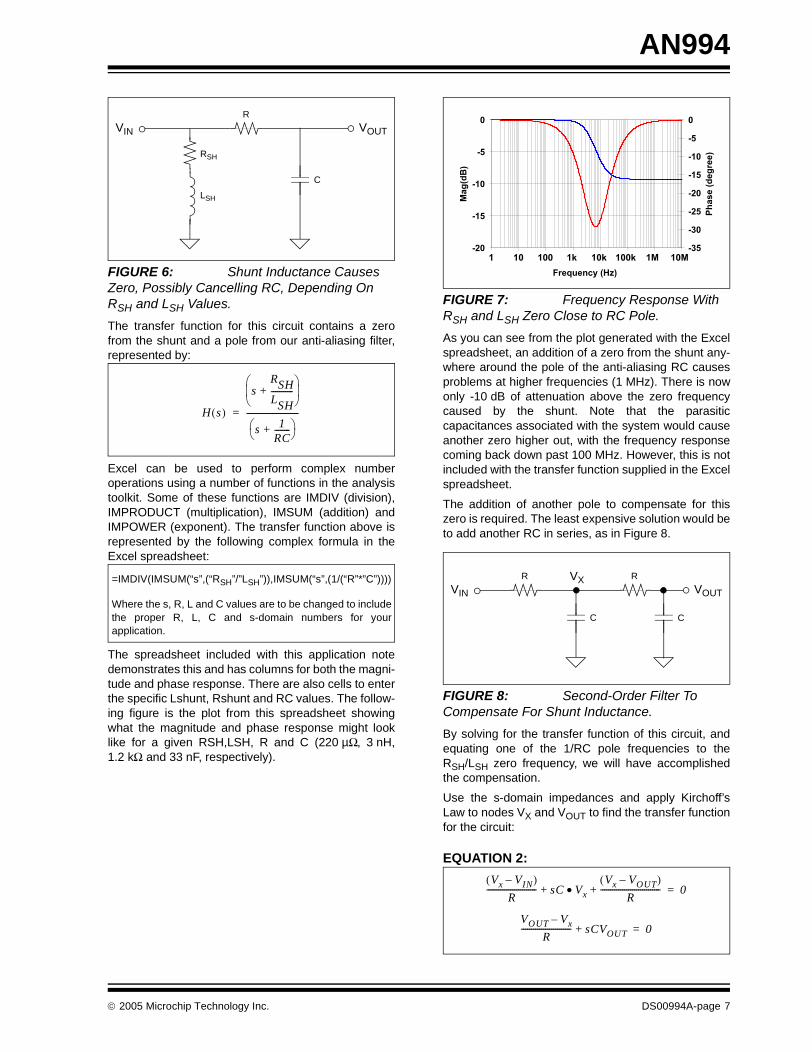
FIGURE 6: Shunt Inductance Causes Zero, Possibly Cancelling RC, Depending On RSH and LSH Values.
The transfer function for this circuit contains a zerofrom the shunt and a pole from our anti-aliasing filter,represented by:
Excel can be used to perform complex numberoperations using a number of functions in the analysistoolkit. Some of these functions are IMDIV (division),IMPRODUCT (multiplication), IMSUM (addition) andIMPOWER (exponent). The transfer function above isrepresented by the following complex formula in theExcel spreadsheet:
The spreadsheet included with this application notedemonstrates this and has columns for both the magni-tude and phase response. There are also cells to enterthe specific Lshunt, Rshunt and RC values. The follow-ing figure is the plot from this spreadsheet showingwhat the magnitude and phase response might looklike for a given RSH,LSH, R and C (220 µΩ, 3 nH,1.2 kΩ and 33 nF, respectively).
FIGURE 7: Frequency Response With RSH and LSH Zero Close to RC Pole.
As you can see from the plot generated with the Excelspreadsheet, an addition of a zero from the shunt any-where around the pole of the anti-aliasing RC causesproblems at higher frequencies (1 MHz). There is nowonly -10 dB of attenuation above the zero frequencycaused by the shunt. Note that the parasiticcapacitances associated with the system would causeanother zero higher out, with the frequency responsecoming back down past 100 MHz. However, this is notincluded with the transfer function supplied in the Excelspreadsheet.
The addition of another pole to compensate for thiszero is required. The least expensive solution would beto add another RC in series, as in Figure 8.
FIGURE 8: Second-Order Filter To Compensate For Shunt Inductance.
By solving for the transfer function of this circuit, andequating one of the 1/RC pole frequencies to theRSH/LSH zero frequency, we will have accomplishedthe compensation.
Use the s-domain impedances and apply Kirchoff’sLaw to nodes VX and VOUT to find the transfer functionfor the circuit:
EQUATION 2:
VIN VOUT
R
C
RSH
LSH
H s( )
sRSHLSH-----------+
⎝ ⎠⎜ ⎟⎛ ⎞
s 1RC--------+⎝ ⎠
⎛ ⎞--------------------------=
=IMDIV(IMSUM(“s”,(“RSH”/”LSH”)),IMSUM(“s”,(1/(“R”*”C”))))
Where the s, R, L and C values are to be changed to includethe proper R, L, C and s-domain numbers for yourapplication.
-20
-15
-10
-5
0
1.E+0 1.E+1 1.E+2 1.E+3 1.E+4 1.E+5 1.E+6 1.E+7
Frequency (Hz)
Ma
g(d
B)
-35
-30
-25
-20
-15
-10
-5
0
Ph
as
e (
de
gre
e)
10k 100k 1M 10M1k100101
VIN VOUT
R
C
R
C
VX
Vx VIN–( )R
------------------------- sC Vx
Vx VOUT–( )R
------------------------------+•+ 0=
VOUT Vx–
R------------------------- sCVOUT+ 0=
© 2005 Microchip Technology Inc. DS00994A-page 7
AN994
Solving for VOUT/VIN:
EQUATION 3:
Solving for the roots of this second equation require theuse of the quadratic formula:
EQUATION 4:
One of the two roots for the equation must be used tocancel the high-pass filter effect caused by the shuntinductance and resistance. By using the shunt zero andpicking an arbitrary capacitor value (C), solve for R:
EQUATION 5:
The location of the other pole is given by the other rootof the quadratic equation solution.
EQUATION 6:
The values for the second-order RC can now be calcu-lated and put into the Excel spreadsheet to evaluatethe performance of the compensation circuit. A second-order filter is also included in the transfer function in theExcel spreadsheet that accompanies this applicationnote. The transfer function and formula using thecomplex number Excel notion is shown here:
EQUATION 7:
In Excel:
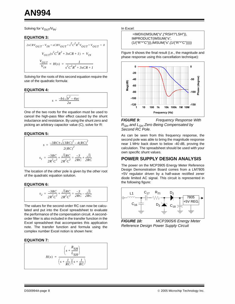
Figure 9 shows the final result (i.e., the magnitude andphase response using this cancellation technique):
FIGURE 9: Frequency Response With RSH and LSH Zero Being Compensated by Second RC Pole.
As can be seen from this frequency response, thesecond pole was able to bring the magnitude responsenear 1 MHz back down to below -40 dB, proving thecalculation. The spreadsheet should be used with yourown specific shunt values.
POWER SUPPLY DESIGN ANALYSISThe power on the MCP3905 Energy Meter ReferenceDesign Demonstration Board comes from a LM7805+5V regulator driven by a half-wave rectified zenerdiode limited AC signal. This circuit is represented inthe following figure:
FIGURE 10: MCP3905/6 Energy Meter Reference Design Power Supply Circuit
2sCRVOUT VIN sCRVOUT s2
C2
R2
VOUT VOUT+++– 0=
VOUT s2C
2R
23sCR 1+ +( ) VIN=
VOUT
VIN------------- H s( ) 1
s2C
2R
23sCR 1+ +
------------------------------------------------= =
sb b
24ac–±–
2a-----------------------------------=
s3RC 3RC( )2
4 RC( )2–±–
2 RC( )2------------------------------------------------------------------=
s13RC–
2R2C
2---------------- 5RC
2R2C
2---------------- 3–
2RC----------- 5
2RC-----------+=+=
s23RC–
2R2C
2---------------- 5RC
2R2C
2---------------- 3–
2RC----------- 5
2RC-----------–=+=
H s( )
sRSHLSH-----------+
⎝ ⎠⎜ ⎟⎛ ⎞
s 1RC--------+⎝ ⎠
⎛ ⎞ s 1RC--------+⎝ ⎠
⎛ ⎞----------------------------------------------=
=IMDIV(IMSUM(“s”,(“RSH”/”LSH”)),IMPRODUCT(IMSUM(“s”,(1/(“R”*”C”))),IMSUM(“s”,(1/(“R”*”C”)))))
-120
-100
-80
-60
-40
-20
0
1.E+0 1.E+1 1.E+2 1.E+3 1.E+4 1.E+5 1.E+6 1.E+7
Frequency (Hz)
Mag
(dB
)
-150
-100
-50
0
Ph
ase (
deg
ree)
10k 100k 1M 10M1k100101
R21
D3 C18
L1
C16
C17 D27805
+5V REG.
DS00994A-page 8 © 2005 Microchip Technology Inc.

AN994
The high-voltage capacitors C16 and C17 divide the linevoltage down with a peak current through C17 given bythe following equations; for a line voltage of 220V, a linefrequency of 50 Hz and a C17 capacitor value of0.47 µF:
EQUATION 8:
The presence of diode D2 leads to the half-wave,rectified waveform shown in Figure 11. This current willcharge capacitor C18, required to hold an average DCvoltage of 14V to completely drive the input to the 5Vregulator LM7805. It is important to analyze the aver-age charging current of this capacitor (C18) whendesigning system power limitations, especially atsystem power-up. This analysis can also be used toreduce capacitor values and board cost, depending onthe current requirements for your system.
FIGURE 11: Half-wave rectified wave-form charging C18 supplies input voltage for regulator and power for meter.
The average current of this half-wave, rectified sinewave is a ratio of 1/π to that of a full sine wave. Theaverage current is calculated from the peak current inthat manner.
Table 7 gives IAVERAGE values for different line voltagesand for 60 Hz line frequencies. For a 50 Hz line cycle,the average values in the table drop by 50/60 (or83.3%). An example using 220V, C17 = 0.47 µF and a50 Hz line cycle frequency would give an IAVERAGE of14.16 mA.
TABLE 7: CHARGING VALUES, 60 HZ LINE
The average current presented here charges C18,which supplies power to the regulator and the rest ofthe meter. During system power-up conditions, if toomuch current is required from your system during thistime, capacitor C18 will not build enough charge andthe regulator will not be fully turned on. The totaldischarge current for your system must not be greaterthan the average current charging C18 during this time.
Zener diode D1 limits the voltage at C18 to 14V, at whichtime D3 is completely turned on. It is necessary to knowthe number of line cycles required to charge C18 to 14V,as this is used in determining system power-upschemes for your application, as well as MCP3905Power-On Reset (POR) conditions. Again, here we areusing the 220V, 50 Hz numbers, with C18 = 470 µF.
EQUATION 9:
Table 8 shows how many line cycle events are requiredto reach 14V at different line voltages, line frequenciesand C17 values. The MCP3905 Energy MeterReference Design Demonstration Board comes popu-lated with a C18 value of 470 µF for a 220V line voltage.If desired, the above formulas can be used to reducethe size of C18 and subsequent board cost.
TABLE 8: C18 CHARGING CYCLES
To further simplify your power supply circuit, you canalso use the formulas to predict a rise from a differentvoltage level or zener diode level. Most devices in yoursystem will have a POR circuit that keeps the device inreset until it hits a certain voltage. For example, tocomplete a rise from 7V, where VDD is regulated to 5V,to a voltage of 14V, you can use:
VRMS C17 IPEAK IAVERAGE
250 0.47μF 0.63 0.20
220 0.47μF 0.55 0.17
180 0.47μF 0.45 0.14
117 1.0 μF 0.62 0.20
110 1.0 μF 0.59 0.19
100 1.0 μF 0.53 0.17
I Cdvdt------ C
d Vsin ωt( )[ ]dt
----------------------------= =
C Vω• ωt( )cos•=0.47μF( ) 220( ) 2( ) 2π( ) 50( ) 1( )cos=
45.9mA (peak)=
VRMS Line C17IAVERAGE on C18
# Cycles to 14V on
C18
250 50 Hz 0.47 µF 0.017 23
220 50 Hz 0.47 µF 0.015 26
180 50 Hz 0.47 µF 0.012 33
130 60 Hz 1.0 µF 0.013 30
110 60 Hz 1.0 µF 0.011 35
90 60 Hz 1.0 µF 0.009 44
I CdVdt-------=
VCHARGE
IAVERAGE T•C
---------------------------------= NCYCLES14V
VCHARGE------------------------=
NCYCLES14
0.61---------- 23 line cycles= =
V t( ) 1C---- IC
o
T
∫ dt=
VCHARGE14.16mA( ) 20ms( )•
470μF( )--------------------------------------------------- 0.61V= =
(14-7)/0.61 = 12 cycles =>12 *20ms = 0.24 seconds
© 2005 Microchip Technology Inc. DS00994A-page 9

AN994
The IEC standard states that the meter should bepowered and functional 5 seconds after the referencevoltage is applied to the terminals (IEC62053, Part 21,Section 8.3.1). The MCP3905 has a POR delay of 1second; neither the HFOUT for LED drive or the F0/F1for the mechanical counter drive will occur during thistime.
Current Budget
When changing the power supply design (in this case,capacitor values totaling the system current require-ments are necessary). The MCP3905 has typical IDDDand IDDA specifications of 1.2 and 3.0 mA, respectively.Assuming there is an output LED on the MCP3905, aswell as a mechanical counter with a 400 ohm coil forthe two-step motor, the current budget would be:
EQUATION 10:
The current required during the system start-up chargetime of C18 represents a discharge current for thiscapacitor. Thus, the total system current for the circuitcannot be larger than the value of IAVERAGE given inTable 8. When this situation arises, the charge on C18will completely turn on the regulator, possibly causingsystem brown-out conditions to occur. The followingscope plot shows the effect of sagging line voltage, thecurrent demands and the effect on the power supplycircuit.
FIGURE 12: Waveforms of power showing increased current demand effects on the power supply.
Channel 2 is the unregulated voltage at the input to theLM7805 (or the voltage on C18). The triangle waveformwas generated to simulate a sagging line voltageacross a very long period (in this case, a period of 20seconds). The pulses on channel 4 are the mechanical
counter pulses on F0 from the MCP3905.The channel2 ripple shows the effect of the 0,1 pulses to turn themechanical counter on the unregulated C18 voltage.The sags in this voltage coincide with the increasedcurrent demand of the system (in this case, the 0,1pulses).
MCP3905 POWER-ON RESET (POR)
The MCP3905 has a POR delay of 1 second. Duringbrown-out, in order to prevent false pulses, this 1second delay is reset and restarted (i.e., any pulses outof the MCP3905 are delayed until the POR timer iscomplete).
This POR timing is shown in Figure 13.
FIGURE 13: Power-on Reset Operation.
NO-LOAD THRESHOLD
Energy meter standards state that when there is noload connected to an energy meter, the device shouldnot slowly register energy. For the MCP3905, this isachieved by placing a threshold-detection circuit belowthe minimum load requirement (start-up current). Thisis defined as 0.0015% of the full-scale output frequencyset by pins f2, f1 and f0. When testing the no-load,IEC62053 states that no more than one pulse shouldoccur during the time (Δt) given here:
EQUATION 11:
For example, using the calibration output pulse with ameter constant of 3200 imp/kWh, a line voltage of 220Vand a maximum current of 80A, the period is about 17minutes.
3mA 1.2mA 4mA 12.5mA+ + +=20.7mA=
ITOTAL IDDA IDDD ILED ISTEPPER MOTOR+ + +=
AVDD
5V4.2V
4V
0V
DEVICEMODE
RESET PROPEROPERATION
RESETNO
PULSEOUT
Time
1s
Where:
k = The meter constant in impulses per kilo-watt hour (im/kWh)
Un = The reference voltage in voltsImax = The maximum current of the meterm = The number of measuring elements
tΔ 600 106×
kmUnImax------------------------- min[ ]≥
DS00994A-page 10 © 2005 Microchip Technology Inc.
AN994
STARTING CURRENT
The IEC standard also defines the smallest current thatthe meter shall be able to register energy for. Thestandard states that the meter “shall start and continueto register at the starting current values” defined. Thesecurrent values are shown in Table 9.
TABLE 9: STARTING CURRENT
As an example, for a Class 1 direct-connect meter witha base current of 10 amperes, the starting currentwould be 40 mA.
MCP3905 VREF TEMPERATURE COEFFICIENT CURVE FITTING
The MCP3905 contains a very low-drift voltagereference. The band gap is specially designed to allowthe signature bow across temperate to be trimmed-in togive the lowest drift across the industrial temperaturerange. Figure 14 shows the effects of this curve fittingand how the low tempco specification of the voltagereference is achieved.
FIGURE 14: Band Gap Curve fitting.
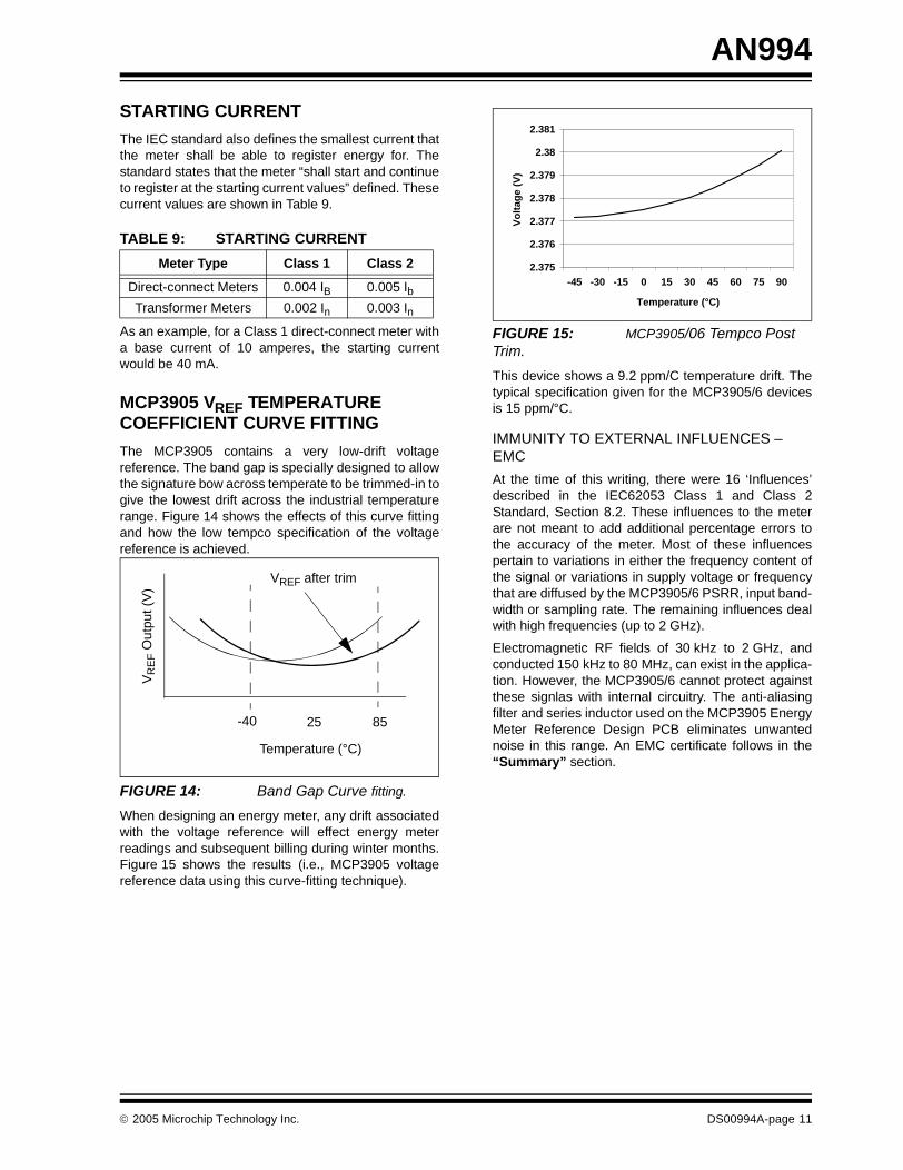
When designing an energy meter, any drift associatedwith the voltage reference will effect energy meterreadings and subsequent billing during winter months.Figure 15 shows the results (i.e., MCP3905 voltagereference data using this curve-fitting technique).
FIGURE 15: MCP3905/06 Tempco Post Trim.
This device shows a 9.2 ppm/C temperature drift. Thetypical specification given for the MCP3905/6 devicesis 15 ppm/°C.
IMMUNITY TO EXTERNAL INFLUENCES – EMC
At the time of this writing, there were 16 ‘Influences’described in the IEC62053 Class 1 and Class 2Standard, Section 8.2. These influences to the meterare not meant to add additional percentage errors tothe accuracy of the meter. Most of these influencespertain to variations in either the frequency content ofthe signal or variations in supply voltage or frequencythat are diffused by the MCP3905/6 PSRR, input band-width or sampling rate. The remaining influences dealwith high frequencies (up to 2 GHz).
Electromagnetic RF fields of 30 kHz to 2 GHz, andconducted 150 kHz to 80 MHz, can exist in the applica-tion. However, the MCP3905/6 cannot protect againstthese signlas with internal circuitry. The anti-aliasingfilter and series inductor used on the MCP3905 EnergyMeter Reference Design PCB eliminates unwantednoise in this range. An EMC certificate follows in the“Summary” section.
Meter Type Class 1 Class 2
Direct-connect Meters 0.004 IB 0.005 IbTransformer Meters 0.002 In 0.003 In
-40 8525
Temperature (°C)
VR
EF O
utpu
t (V
)
VREF after trim
2.375
2.376
2.377
2.378
2.379
2.38
2.381
-45 -30 -15 0 15 30 45 60 75 90
Temperature (°C)
Vo
ltag
e (V
)
© 2005 Microchip Technology Inc. DS00994A-page 11
AN994
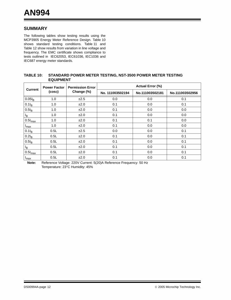
SUMMARY
The following tables show testing results using theMCP3905 Energy Meter Reference Design. Table 10shows standard testing conditions. Table 11 andTable 12 show results from variation in line voltage andfrequency. The EMC certificate shows compliance totests outlined in IEC62053, IEC61036, IEC1036 andIEC687 energy meter standards.
TABLE 10: STANDARD POWER METER TESTING, NST-3500 POWER METER TESTING EQUIPMENT
CurrentPower Factor
(cosφ)Permission Error
Change (%)
Actual Error (%)
No. 111003502194 No.111003502181 No.111003502956
0.05IB 1.0 ±2.5 0.0 0.0 0.1
0.1IB 1.0 ±2.0 0.1 0.0 0.1
0.5IB 1.0 ±2.0 0.1 0.0 0.0
IB 1.0 ±2.0 0.1 0.0 0.0
0.5Imax 1.0 ±2.0 0.1 0.1 0.0
Imax 1.0 ±2.0 0.1 0.0 0.0
0.1IB 0.5L ±2.5 0.0 0.0 0.1
0.2IB 0.5L ±2.0 0.1 0.0 0.1
0.5IB 0.5L ±2.0 0.1 0.0 0.1
IB 0.5L ±2.0 0.1 0.0 0.1
0.5Imax 0.5L ±2.0 0.1 0.0 0.1
Imax 0.5L ±2.0 0.1 0.0 0.1
Note: Reference Voltage: 220V Current: 5(20)A Reference Frequency: 50 HzTemperature: 23°C Humidity: 45%
DS00994A-page 12 © 2005 Microchip Technology Inc.

AN994
TABLE 11: FREQUENCY ERROR TESTING RESULTS, NST-3500 METER TESTING EQUIPMENT
TABLE 12: VOLTAGE ERROR TESTING RESULTS, NST-3500 METER TESTING EQUIPMENT
CurrentPower Factor
(cosφ)Frequency
(Hz)Permission Error
Change (%)
Actual Error Changing (%)
#1
0.05IB1.0
49
±0.5
0.065
IB 0.046
Imax 0.000
0.1IB0.5L ±0.7
-0.016
IB -0.014
Imax -0.034
0.05IB1.0
51
±0.5
0.121
IB 0.067
Imax 0.054
0.1Ib0.5L ±0.7
0.056
IB 0.042
Imax 0.026
Note: Reference Voltage: 220V Current (IB): 10A Reference Frequency: 50 HzTemperature: 23°C Humidity: 45%
CurrentPower Factor
(cosφ)Voltage
(V)Permission Error
Change (%)
Actual Error Changing(%)
#1
0.05IB 1.0 198 ±0.7 -0.071
IB 0.063
Imax 0.032
0.1IB 0.5L ±1.0 0.052
IB 0.030
Imax 0.016
0.05IB 1.0 242 ±0.7 -0.017
IB 0.000
Imax -0.030
0.1IB 0.5L ±1.0 -0.015
IB -0.014
Imax -0.047
Note: Reference Voltage: 220V Current (IB): 10A Reference Frequency: 50 HzTemperature: 23°C Humidity: 45%
© 2005 Microchip Technology Inc. DS00994A-page 13

AN994
Certificate of EMC Compliance
DS00994A-page 14 © 2005 Microchip Technology Inc.
AN994
REFERENCES
[1] Steven R. Norsworthy, Richard Schreier, Gabor C.Temes, “Delta-Sigma Data Converters Theory,Design and Simulation”, IEEE Press, 1997, p. 4-9.
[2] David Jarman, “A Brief Introduction to Delta-SigmaConverters”, Intersil Application Note, 1995.
[3] “New Current-Sensing Scheme for Static TransferSwitches”, Solid State Controls technicalwhitepaper.
[4] “IEC 62053 Standard”, IEC Commission, 2003.
© 2005 Microchip Technology Inc. DS00994A-page 15
AN994
NOTES:
DS00994A-page 16 © 2005 Microchip Technology Inc.

Note the following details of the code protection feature on Microchip devices:
• Microchip products meet the specification contained in their particular Microchip Data Sheet.
• Microchip believes that its family of products is one of the most secure families of its kind on the market today, when used in the intended manner and under normal conditions.
• There are dishonest and possibly illegal methods used to breach the code protection feature. All of these methods, to our knowledge, require using the Microchip products in a manner outside the operating specifications contained in Microchip’s Data Sheets. Most likely, the person doing so is engaged in theft of intellectual property.
• Microchip is willing to work with the customer who is concerned about the integrity of their code.
• Neither Microchip nor any other semiconductor manufacturer can guarantee the security of their code. Code protection does not mean that we are guaranteeing the product as “unbreakable.”
Code protection is constantly evolving. We at Microchip are committed to continuously improving the code protection features of ourproducts. Attempts to break Microchip’s code protection feature may be a violation of the Digital Millennium Copyright Act. If such actsallow unauthorized access to your software or other copyrighted work, you may have a right to sue for relief under that Act.
Information contained in this publication regarding deviceapplications and the like is provided only for your convenienceand may be superseded by updates. It is your responsibility toensure that your application meets with your specifications.MICROCHIP MAKES NO REPRESENTATIONS OR WAR-RANTIES OF ANY KIND WHETHER EXPRESS OR IMPLIED,WRITTEN OR ORAL, STATUTORY OR OTHERWISE,RELATED TO THE INFORMATION, INCLUDING BUT NOTLIMITED TO ITS CONDITION, QUALITY, PERFORMANCE,MERCHANTABILITY OR FITNESS FOR PURPOSE.Microchip disclaims all liability arising from this information andits use. Use of Microchip’s products as critical components inlife support systems is not authorized except with expresswritten approval by Microchip. No licenses are conveyed,implicitly or otherwise, under any Microchip intellectual propertyrights.
© 2005 Microchip Technology Inc.
Trademarks
The Microchip name and logo, the Microchip logo, Accuron, dsPIC, KEELOQ, microID, MPLAB, PIC, PICmicro, PICSTART, PRO MATE, PowerSmart, rfPIC, and SmartShunt are registered trademarks of Microchip Technology Incorporated in the U.S.A. and other countries.
AmpLab, FilterLab, Migratable Memory, MXDEV, MXLAB, PICMASTER, SEEVAL, SmartSensor and The Embedded Control Solutions Company are registered trademarks of Microchip Technology Incorporated in the U.S.A.
Analog-for-the-Digital Age, Application Maestro, dsPICDEM, dsPICDEM.net, dsPICworks, ECAN, ECONOMONITOR, FanSense, FlexROM, fuzzyLAB, In-Circuit Serial Programming, ICSP, ICEPIC, Linear Active Thermistor, MPASM, MPLIB, MPLINK, MPSIM, PICkit, PICDEM, PICDEM.net, PICLAB, PICtail, PowerCal, PowerInfo, PowerMate, PowerTool, rfLAB, rfPICDEM, Select Mode, Smart Serial, SmartTel, Total Endurance and WiperLock are trademarks of Microchip Technology Incorporated in the U.S.A. and other countries.
SQTP is a service mark of Microchip Technology Incorporated in the U.S.A.
All other trademarks mentioned herein are property of their respective companies.
© 2005, Microchip Technology Incorporated, Printed in the U.S.A., All Rights Reserved.
Printed on recycled paper.
DS00994A-page 17
Microchip received ISO/TS-16949:2002 quality system certification for its worldwide headquarters, design and wafer fabrication facilities in Chandler and Tempe, Arizona and Mountain View, California in October 2003. The Company’s quality system processes and procedures are for its PICmicro® 8-bit MCUs, KEELOQ® code hopping devices, Serial EEPROMs, microperipherals, nonvolatile memory and analog products. In addition, Microchip’s quality system for the design and manufacture of development systems is ISO 9001:2000 certified.

DS00994A-page 18 © 2005 Microchip Technology Inc.
AMERICASCorporate Office2355 West Chandler Blvd.Chandler, AZ 85224-6199Tel: 480-792-7200 Fax: 480-792-7277Technical Support: http://support.microchip.comWeb Address: www.microchip.com
AtlantaAlpharetta, GA Tel: 770-640-0034 Fax: 770-640-0307
BostonWestborough, MA Tel: 774-760-0087 Fax: 774-760-0088
ChicagoItasca, IL Tel: 630-285-0071 Fax: 630-285-0075
DallasAddison, TX Tel: 972-818-7423 Fax: 972-818-2924
DetroitFarmington Hills, MI Tel: 248-538-2250Fax: 248-538-2260
KokomoKokomo, IN Tel: 765-864-8360Fax: 765-864-8387
Los AngelesMission Viejo, CA Tel: 949-462-9523 Fax: 949-462-9608
San JoseMountain View, CA Tel: 650-215-1444Fax: 650-961-0286
TorontoMississauga, Ontario, CanadaTel: 905-673-0699 Fax: 905-673-6509
ASIA/PACIFICAustralia - SydneyTel: 61-2-9868-6733 Fax: 61-2-9868-6755
China - BeijingTel: 86-10-8528-2100 Fax: 86-10-8528-2104
China - ChengduTel: 86-28-8676-6200 Fax: 86-28-8676-6599
China - FuzhouTel: 86-591-8750-3506 Fax: 86-591-8750-3521
China - Hong Kong SARTel: 852-2401-1200 Fax: 852-2401-3431
China - QingdaoTel: 86-532-502-7355 Fax: 86-532-502-7205
China - ShanghaiTel: 86-21-5407-5533 Fax: 86-21-5407-5066China - ShenyangTel: 86-24-2334-2829Fax: 86-24-2334-2393
China - ShenzhenTel: 86-755-8203-2660 Fax: 86-755-8203-1760
China - ShundeTel: 86-757-2839-5507 Fax: 86-757-2839-5571
China - WuhanTel: 86-27-5980-5300Fax: 86-27-5980-5118
China - XianTel: 86-29-8833-7250Fax: 86-29-8833-7256
ASIA/PACIFICIndia - BangaloreTel: 91-80-2229-0061 Fax: 91-80-2229-0062
India - New DelhiTel: 91-11-5160-8631Fax: 91-11-5160-8632
India - PuneTel: 91-20-2566-1512Fax: 91-20-2566-1513
Japan - YokohamaTel: 81-45-471- 6166 Fax: 81-45-471-6122
Korea - SeoulTel: 82-2-554-7200 Fax: 82-2-558-5932 or 82-2-558-5934
Malaysia - PenangTel: 604-646-8870Fax: 604-646-5086
Philippines - ManilaTel: 011-632-634-9065Fax: 011-632-634-9069
SingaporeTel: 65-6334-8870 Fax: 65-6334-8850
Taiwan - HsinchuTel: 886-3-572-9526Fax: 886-3-572-6459
Taiwan - KaohsiungTel: 886-7-536-4818Fax: 886-7-536-4803
Taiwan - TaipeiTel: 886-2-2500-6610 Fax: 886-2-2508-0102
Thailand - BangkokTel: 66-2-694-1351Fax: 66-2-694-1350
EUROPEAustria - WeisTel: 43-7242-2244-399Fax: 43-7242-2244-393Denmark - CopenhagenTel: 45-4450-2828 Fax: 45-4485-2829
France - ParisTel: 33-1-69-53-63-20 Fax: 33-1-69-30-90-79
Germany - MunichTel: 49-89-627-144-0 Fax: 49-89-627-144-44
Italy - Milan Tel: 39-0331-742611 Fax: 39-0331-466781
Netherlands - DrunenTel: 31-416-690399 Fax: 31-416-690340
Spain - MadridTel: 34-91-352-30-52Fax: 34-91-352-11-47
UK - WokinghamTel: 44-118-921-5869Fax: 44-118-921-5820
WORLDWIDE SALES AND SERVICE
07/01/05