
IDT Tsi381 PCIe -to-PCI Bridge User Manual
271
® IDT ® Tsi381 PCIe ® -to-PCI Bridge User Manual April 16, 2014
Transcript of IDT Tsi381 PCIe -to-PCI Bridge User Manual

®
IDT®
Tsi381 PCIe®-to-PCI BridgeUser Manual
April 16, 2014

GENERAL DISCLAIMERIntegrated Device Technology, Inc. reserves the right to make changes to its products or specifications at any time, without notice, in order to improve design or performance and to supply the best possible product. IDT does not assume any responsibility for use of any circuitry described other than the circuitry embodied in an IDT product. The Company makes no representations that circuitry described herein is free from patent infringement or other rights of third parties which may result from its use. No license is granted by implication or otherwise under any patent, patent rights or other rights, of Integrated Device Technology, Inc.
CODE DISCLAIMERCode examples provided by IDT are for illustrative purposes only and should not be relied upon for developing applications. Any use of the code examples below is completely at your own risk. IDT MAKES NO REPRESENTATIONS OR WARRANTIES OF ANY KIND CONCERNING THE NONINFRINGEMENT, QUALITY, SAFETY OR SUITABILITY OF THE CODE, EITHER EXPRESS OR IMPLIED, INCLUDING WITHOUT LIMITATION ANY IMPLIED WARRANTIES OF MERCHANTABILITY, FITNESS FOR A PARTICU-LAR PURPOSE, OR NON-INFRINGEMENT. FURTHER, IDT MAKES NO REPRESENTATIONS OR WARRANTIES AS TO THE TRUTH, ACCURACY OR COMPLETENESS OF ANY STATEMENTS, INFORMATION OR MATERIALS CONCERNING CODE EXAMPLES CONTAINED IN ANY IDT PUBLICATION OR PUBLIC DISCLOSURE OR THAT IS CONTAINED ON ANY IDT INTERNET SITE. IN NO EVENT WILL IDT BE LIABLE FOR ANY DIRECT, CONSEQUENTIAL, INCIDENTAL, INDIRECT, PUNITIVE OR SPECIAL DAMAGES, HOWEVER THEY MAY ARISE, AND EVEN IF IDT HAS BEEN PREVIOUSLY ADVISED ABOUT THE POSSIBILITY OF SUCH DAMAGES. The code examples also may be subject to United States export control laws and may be subject to the export or import laws of other countries and it is your responsibility to comply with any applicable laws or regulations.
LIFE SUPPORT POLICYIntegrated Device Technology's products are not authorized for use as critical components in life support devices or systems unless a specific written agreement pertaining to such intended use is executed between the manufacturer and an officer of IDT.1. Life support devices or systems are devices or systems which (a) are intended for surgical implant into the body or (b) support or sustain life and whose failure to perform, when properly used in accordance with instructions for use provided in the labeling, can be reasonably expected to result in a significant injury to the user.2. A critical component is any components of a life support device or system whose failure to perform can be reasonably expected to cause the failure of the life support device or system, or to affect its safety or effectiveness.
IDT, the IDT logo, and Integrated Device Technology are trademarks or registered trademarks of Integrated Device Technology, Inc.

3
Contents
About this Document. . . . . . . . . . . . . . . . . . . . . . . . . . . . . . . . . . . . . . . . . . . . . . . . . . . . 15Scope . . . . . . . . . . . . . . . . . . . . . . . . . . . . . . . . . . . . . . . . . . . . . . . . . . . . . . . . . . . . . . . . . . . . . . . . . . . . . . . . . . . . . . . . . 15
Document Conventions . . . . . . . . . . . . . . . . . . . . . . . . . . . . . . . . . . . . . . . . . . . . . . . . . . . . . . . . . . . . . . . . . . . . . . . . . . . 15
Revision History . . . . . . . . . . . . . . . . . . . . . . . . . . . . . . . . . . . . . . . . . . . . . . . . . . . . . . . . . . . . . . . . . . . . . . . . . . . . . . . . 17
1. Functional Overview . . . . . . . . . . . . . . . . . . . . . . . . . . . . . . . . . . . . . . . . . . . . . . . . 211.1 Overview . . . . . . . . . . . . . . . . . . . . . . . . . . . . . . . . . . . . . . . . . . . . . . . . . . . . . . . . . . . . . . . . . . . . . . . . . . . . . . . . 21
1.2 Features . . . . . . . . . . . . . . . . . . . . . . . . . . . . . . . . . . . . . . . . . . . . . . . . . . . . . . . . . . . . . . . . . . . . . . . . . . . . . . . . . 22
1.2.1 General Features. . . . . . . . . . . . . . . . . . . . . . . . . . . . . . . . . . . . . . . . . . . . . . . . . . . . . . . . . . . . . . . . . . . 22
1.2.2 PCIe Features . . . . . . . . . . . . . . . . . . . . . . . . . . . . . . . . . . . . . . . . . . . . . . . . . . . . . . . . . . . . . . . . . . . . . 23
1.2.3 PCI Features . . . . . . . . . . . . . . . . . . . . . . . . . . . . . . . . . . . . . . . . . . . . . . . . . . . . . . . . . . . . . . . . . . . . . . 23
1.3 Device Architecture . . . . . . . . . . . . . . . . . . . . . . . . . . . . . . . . . . . . . . . . . . . . . . . . . . . . . . . . . . . . . . . . . . . . . . . . 24
1.4 Typical Applications . . . . . . . . . . . . . . . . . . . . . . . . . . . . . . . . . . . . . . . . . . . . . . . . . . . . . . . . . . . . . . . . . . . . . . . 26
2. Signal Descriptions . . . . . . . . . . . . . . . . . . . . . . . . . . . . . . . . . . . . . . . . . . . . . . . . . 292.1 Overview . . . . . . . . . . . . . . . . . . . . . . . . . . . . . . . . . . . . . . . . . . . . . . . . . . . . . . . . . . . . . . . . . . . . . . . . . . . . . . . . 29
2.2 PCIe Interface Signals . . . . . . . . . . . . . . . . . . . . . . . . . . . . . . . . . . . . . . . . . . . . . . . . . . . . . . . . . . . . . . . . . . . . . . 30
2.3 PCI Interface Signals . . . . . . . . . . . . . . . . . . . . . . . . . . . . . . . . . . . . . . . . . . . . . . . . . . . . . . . . . . . . . . . . . . . . . . . 30
2.4 EEPROM Interface Signals . . . . . . . . . . . . . . . . . . . . . . . . . . . . . . . . . . . . . . . . . . . . . . . . . . . . . . . . . . . . . . . . . . 34
2.5 GPIO Signals . . . . . . . . . . . . . . . . . . . . . . . . . . . . . . . . . . . . . . . . . . . . . . . . . . . . . . . . . . . . . . . . . . . . . . . . . . . . . 34
2.6 JTAG Interface Signals . . . . . . . . . . . . . . . . . . . . . . . . . . . . . . . . . . . . . . . . . . . . . . . . . . . . . . . . . . . . . . . . . . . . . 34
2.7 Power-up Signals . . . . . . . . . . . . . . . . . . . . . . . . . . . . . . . . . . . . . . . . . . . . . . . . . . . . . . . . . . . . . . . . . . . . . . . . . . 36
2.8 Power Supply Signals . . . . . . . . . . . . . . . . . . . . . . . . . . . . . . . . . . . . . . . . . . . . . . . . . . . . . . . . . . . . . . . . . . . . . . 36
3. Data Path. . . . . . . . . . . . . . . . . . . . . . . . . . . . . . . . . . . . . . . . . . . . . . . . . . . . . . . . . . 373.1 Overview . . . . . . . . . . . . . . . . . . . . . . . . . . . . . . . . . . . . . . . . . . . . . . . . . . . . . . . . . . . . . . . . . . . . . . . . . . . . . . . . 37
3.1.1 Upstream Data Path . . . . . . . . . . . . . . . . . . . . . . . . . . . . . . . . . . . . . . . . . . . . . . . . . . . . . . . . . . . . . . . . 37
3.1.2 Downstream Data Path. . . . . . . . . . . . . . . . . . . . . . . . . . . . . . . . . . . . . . . . . . . . . . . . . . . . . . . . . . . . . . 38
3.2 Transaction Management . . . . . . . . . . . . . . . . . . . . . . . . . . . . . . . . . . . . . . . . . . . . . . . . . . . . . . . . . . . . . . . . . . . . 39
3.2.1 Upstream Transaction Management. . . . . . . . . . . . . . . . . . . . . . . . . . . . . . . . . . . . . . . . . . . . . . . . . . . . 39
3.2.2 Downstream Transaction Management . . . . . . . . . . . . . . . . . . . . . . . . . . . . . . . . . . . . . . . . . . . . . . . . . 40
3.3 Buffer Structure . . . . . . . . . . . . . . . . . . . . . . . . . . . . . . . . . . . . . . . . . . . . . . . . . . . . . . . . . . . . . . . . . . . . . . . . . . . 40
3.3.1 Upstream Non-posted Buffer . . . . . . . . . . . . . . . . . . . . . . . . . . . . . . . . . . . . . . . . . . . . . . . . . . . . . . . . . 40
3.3.2 Upstream Posted Buffer . . . . . . . . . . . . . . . . . . . . . . . . . . . . . . . . . . . . . . . . . . . . . . . . . . . . . . . . . . . . . 41
3.3.3 Downstream Non-posted Buffer . . . . . . . . . . . . . . . . . . . . . . . . . . . . . . . . . . . . . . . . . . . . . . . . . . . . . . 42
3.3.4 Downstream Posted Buffer . . . . . . . . . . . . . . . . . . . . . . . . . . . . . . . . . . . . . . . . . . . . . . . . . . . . . . . . . . 42
3.4 Flow Control . . . . . . . . . . . . . . . . . . . . . . . . . . . . . . . . . . . . . . . . . . . . . . . . . . . . . . . . . . . . . . . . . . . . . . . . . . . . . 42
3.5 Prefetching Algorithm . . . . . . . . . . . . . . . . . . . . . . . . . . . . . . . . . . . . . . . . . . . . . . . . . . . . . . . . . . . . . . . . . . . . . . 43
3.6 Short Term Caching . . . . . . . . . . . . . . . . . . . . . . . . . . . . . . . . . . . . . . . . . . . . . . . . . . . . . . . . . . . . . . . . . . . . . . . . 44
3.7 Polarity Reversal . . . . . . . . . . . . . . . . . . . . . . . . . . . . . . . . . . . . . . . . . . . . . . . . . . . . . . . . . . . . . . . . . . . . . . . . . . 44
Tsi381 User Manual
April 16, 2014
Integrated Device Technology
www.idt.com

Contents4
4. Addressing . . . . . . . . . . . . . . . . . . . . . . . . . . . . . . . . . . . . . . . . . . . . . . . . . . . . . . . . .454.1 Overview . . . . . . . . . . . . . . . . . . . . . . . . . . . . . . . . . . . . . . . . . . . . . . . . . . . . . . . . . . . . . . . . . . . . . . . . . . . . . . . . 45
4.2 Memory-mapped I/O Space. . . . . . . . . . . . . . . . . . . . . . . . . . . . . . . . . . . . . . . . . . . . . . . . . . . . . . . . . . . . . . . . . . 45
4.3 Prefetchable Space. . . . . . . . . . . . . . . . . . . . . . . . . . . . . . . . . . . . . . . . . . . . . . . . . . . . . . . . . . . . . . . . . . . . . . . . . 47
4.4 I/O Space . . . . . . . . . . . . . . . . . . . . . . . . . . . . . . . . . . . . . . . . . . . . . . . . . . . . . . . . . . . . . . . . . . . . . . . . . . . . . . . . 48
4.5 VGA Addressing . . . . . . . . . . . . . . . . . . . . . . . . . . . . . . . . . . . . . . . . . . . . . . . . . . . . . . . . . . . . . . . . . . . . . . . . . . 50
4.6 ISA Addressing . . . . . . . . . . . . . . . . . . . . . . . . . . . . . . . . . . . . . . . . . . . . . . . . . . . . . . . . . . . . . . . . . . . . . . . . . . . 50
4.7 Non-transparent Addressing . . . . . . . . . . . . . . . . . . . . . . . . . . . . . . . . . . . . . . . . . . . . . . . . . . . . . . . . . . . . . . . . . 51
4.7.1 PCIe to PCI Non-prefetchable Address Remapping . . . . . . . . . . . . . . . . . . . . . . . . . . . . . . . . . . . . . . . 52
4.7.2 PCIe to PCI Prefetchable Address Remapping . . . . . . . . . . . . . . . . . . . . . . . . . . . . . . . . . . . . . . . . . . . 52
4.7.3 PCI to PCIe Address Remapping. . . . . . . . . . . . . . . . . . . . . . . . . . . . . . . . . . . . . . . . . . . . . . . . . . . . . . 53
4.8 Opaque Addressing . . . . . . . . . . . . . . . . . . . . . . . . . . . . . . . . . . . . . . . . . . . . . . . . . . . . . . . . . . . . . . . . . . . . . . . . 55
5. Configuration Transactions . . . . . . . . . . . . . . . . . . . . . . . . . . . . . . . . . . . . . . . . . . .575.1 Overview . . . . . . . . . . . . . . . . . . . . . . . . . . . . . . . . . . . . . . . . . . . . . . . . . . . . . . . . . . . . . . . . . . . . . . . . . . . . . . . . 57
5.2 Configuration Transactions . . . . . . . . . . . . . . . . . . . . . . . . . . . . . . . . . . . . . . . . . . . . . . . . . . . . . . . . . . . . . . . . . . 57
5.2.1 Type 0 Configuration Transactions . . . . . . . . . . . . . . . . . . . . . . . . . . . . . . . . . . . . . . . . . . . . . . . . . . . . 58
5.2.2 Type 1 Configuration Transactions . . . . . . . . . . . . . . . . . . . . . . . . . . . . . . . . . . . . . . . . . . . . . . . . . . . . 58
5.2.3 Type 1 to Type 0 Conversion . . . . . . . . . . . . . . . . . . . . . . . . . . . . . . . . . . . . . . . . . . . . . . . . . . . . . . . . . 59
5.2.4 Type 1 to Type 1 Forwarding. . . . . . . . . . . . . . . . . . . . . . . . . . . . . . . . . . . . . . . . . . . . . . . . . . . . . . . . . 59
5.2.5 Type 1 to Special Cycle Forwarding . . . . . . . . . . . . . . . . . . . . . . . . . . . . . . . . . . . . . . . . . . . . . . . . . . . 60
5.3 PCIe Enhanced Configuration Mechanism . . . . . . . . . . . . . . . . . . . . . . . . . . . . . . . . . . . . . . . . . . . . . . . . . . . . . . 60
5.4 Configuration Retry Mechanisms . . . . . . . . . . . . . . . . . . . . . . . . . . . . . . . . . . . . . . . . . . . . . . . . . . . . . . . . . . . . . 61
6. Bridging . . . . . . . . . . . . . . . . . . . . . . . . . . . . . . . . . . . . . . . . . . . . . . . . . . . . . . . . . . .636.1 Overview . . . . . . . . . . . . . . . . . . . . . . . . . . . . . . . . . . . . . . . . . . . . . . . . . . . . . . . . . . . . . . . . . . . . . . . . . . . . . . . . 63
6.2 Flow Control Advertisements . . . . . . . . . . . . . . . . . . . . . . . . . . . . . . . . . . . . . . . . . . . . . . . . . . . . . . . . . . . . . . . . 63
6.3 Buffer Size and Management . . . . . . . . . . . . . . . . . . . . . . . . . . . . . . . . . . . . . . . . . . . . . . . . . . . . . . . . . . . . . . . . 64
6.4 Assignment of Requestor ID and Tag . . . . . . . . . . . . . . . . . . . . . . . . . . . . . . . . . . . . . . . . . . . . . . . . . . . . . . . . . . 64
6.5 Forwarding of PCIe to PCI . . . . . . . . . . . . . . . . . . . . . . . . . . . . . . . . . . . . . . . . . . . . . . . . . . . . . . . . . . . . . . . . . . 64
6.5.1 PCIe Memory Write Request. . . . . . . . . . . . . . . . . . . . . . . . . . . . . . . . . . . . . . . . . . . . . . . . . . . . . . . . . 64
6.5.2 PCIe Non-posted Requests . . . . . . . . . . . . . . . . . . . . . . . . . . . . . . . . . . . . . . . . . . . . . . . . . . . . . . . . . . 64
6.6 Forwarding of PCI to PCIe . . . . . . . . . . . . . . . . . . . . . . . . . . . . . . . . . . . . . . . . . . . . . . . . . . . . . . . . . . . . . . . . . . 65
6.6.1 PCI Memory Write Request. . . . . . . . . . . . . . . . . . . . . . . . . . . . . . . . . . . . . . . . . . . . . . . . . . . . . . . . . . 65
6.6.2 PCI Non-posted Requests . . . . . . . . . . . . . . . . . . . . . . . . . . . . . . . . . . . . . . . . . . . . . . . . . . . . . . . . . . . 66
6.7 PCI Transaction Support . . . . . . . . . . . . . . . . . . . . . . . . . . . . . . . . . . . . . . . . . . . . . . . . . . . . . . . . . . . . . . . . . . . . 67
6.8 PCIe Transaction Support . . . . . . . . . . . . . . . . . . . . . . . . . . . . . . . . . . . . . . . . . . . . . . . . . . . . . . . . . . . . . . . . . . . 68
6.9 Message Transactions . . . . . . . . . . . . . . . . . . . . . . . . . . . . . . . . . . . . . . . . . . . . . . . . . . . . . . . . . . . . . . . . . . . . . . 69
6.9.1 INTx Interrupt Signaling . . . . . . . . . . . . . . . . . . . . . . . . . . . . . . . . . . . . . . . . . . . . . . . . . . . . . . . . . . . . 69
6.9.2 Power Management . . . . . . . . . . . . . . . . . . . . . . . . . . . . . . . . . . . . . . . . . . . . . . . . . . . . . . . . . . . . . . . . 69
6.9.3 Locked Transaction . . . . . . . . . . . . . . . . . . . . . . . . . . . . . . . . . . . . . . . . . . . . . . . . . . . . . . . . . . . . . . . . 69
6.9.4 Slot Power Limit . . . . . . . . . . . . . . . . . . . . . . . . . . . . . . . . . . . . . . . . . . . . . . . . . . . . . . . . . . . . . . . . . . 69
6.9.5 Vendor-defined and Device ID . . . . . . . . . . . . . . . . . . . . . . . . . . . . . . . . . . . . . . . . . . . . . . . . . . . . . . . 69
6.10 Transaction Ordering . . . . . . . . . . . . . . . . . . . . . . . . . . . . . . . . . . . . . . . . . . . . . . . . . . . . . . . . . . . . . . . . . . . . . . . 70
6.11 Exclusive Access . . . . . . . . . . . . . . . . . . . . . . . . . . . . . . . . . . . . . . . . . . . . . . . . . . . . . . . . . . . . . . . . . . . . . . . . . . 71
Tsi381 User Manual
April 16, 2014
Integrated Device Technology
www.idt.com

Contents 5
7. PCI Arbitration . . . . . . . . . . . . . . . . . . . . . . . . . . . . . . . . . . . . . . . . . . . . . . . . . . . . . 737.1 Overview . . . . . . . . . . . . . . . . . . . . . . . . . . . . . . . . . . . . . . . . . . . . . . . . . . . . . . . . . . . . . . . . . . . . . . . . . . . . . . . . 73
7.2 Block Diagram . . . . . . . . . . . . . . . . . . . . . . . . . . . . . . . . . . . . . . . . . . . . . . . . . . . . . . . . . . . . . . . . . . . . . . . . . . . . 73
7.3 PCI Arbitration Scheme . . . . . . . . . . . . . . . . . . . . . . . . . . . . . . . . . . . . . . . . . . . . . . . . . . . . . . . . . . . . . . . . . . . . . 74
8. Interrupt Handling . . . . . . . . . . . . . . . . . . . . . . . . . . . . . . . . . . . . . . . . . . . . . . . . . . 778.1 Overview . . . . . . . . . . . . . . . . . . . . . . . . . . . . . . . . . . . . . . . . . . . . . . . . . . . . . . . . . . . . . . . . . . . . . . . . . . . . . . . . 77
8.2 Interrupt Sources . . . . . . . . . . . . . . . . . . . . . . . . . . . . . . . . . . . . . . . . . . . . . . . . . . . . . . . . . . . . . . . . . . . . . . . . . . 78
8.3 Interrupt Routing . . . . . . . . . . . . . . . . . . . . . . . . . . . . . . . . . . . . . . . . . . . . . . . . . . . . . . . . . . . . . . . . . . . . . . . . . . 78
8.4 MSI Generation using GPIOs and Interrupts . . . . . . . . . . . . . . . . . . . . . . . . . . . . . . . . . . . . . . . . . . . . . . . . . . . . . 78
9. Error Handling . . . . . . . . . . . . . . . . . . . . . . . . . . . . . . . . . . . . . . . . . . . . . . . . . . . . . 799.1 Overview . . . . . . . . . . . . . . . . . . . . . . . . . . . . . . . . . . . . . . . . . . . . . . . . . . . . . . . . . . . . . . . . . . . . . . . . . . . . . . . . 79
9.2 PCIe as Originating Interface. . . . . . . . . . . . . . . . . . . . . . . . . . . . . . . . . . . . . . . . . . . . . . . . . . . . . . . . . . . . . . . . . 82
9.2.1 Received Poisoned TLPs . . . . . . . . . . . . . . . . . . . . . . . . . . . . . . . . . . . . . . . . . . . . . . . . . . . . . . . . . . . . 83
9.2.2 Received ECRC Errors . . . . . . . . . . . . . . . . . . . . . . . . . . . . . . . . . . . . . . . . . . . . . . . . . . . . . . . . . . . . . 84
9.2.3 PCI Uncorrectable Data Errors . . . . . . . . . . . . . . . . . . . . . . . . . . . . . . . . . . . . . . . . . . . . . . . . . . . . . . . 85
9.2.4 PCI Uncorrectable Address/Attribute Errors . . . . . . . . . . . . . . . . . . . . . . . . . . . . . . . . . . . . . . . . . . . . . 86
9.2.5 Received Master-Abort on PCI Interface. . . . . . . . . . . . . . . . . . . . . . . . . . . . . . . . . . . . . . . . . . . . . . . . 87
9.2.6 Received Target-Abort On PCI Interface. . . . . . . . . . . . . . . . . . . . . . . . . . . . . . . . . . . . . . . . . . . . . . . . 88
9.3 PCI as Originating Interface. . . . . . . . . . . . . . . . . . . . . . . . . . . . . . . . . . . . . . . . . . . . . . . . . . . . . . . . . . . . . . . . . . 89
9.3.1 Received PCI Errors. . . . . . . . . . . . . . . . . . . . . . . . . . . . . . . . . . . . . . . . . . . . . . . . . . . . . . . . . . . . . . . . 90
9.3.2 Unsupported Request Completion Status. . . . . . . . . . . . . . . . . . . . . . . . . . . . . . . . . . . . . . . . . . . . . . . . 93
9.3.3 Completer Abort Completion Status . . . . . . . . . . . . . . . . . . . . . . . . . . . . . . . . . . . . . . . . . . . . . . . . . . . 93
9.4 Timeout Errors . . . . . . . . . . . . . . . . . . . . . . . . . . . . . . . . . . . . . . . . . . . . . . . . . . . . . . . . . . . . . . . . . . . . . . . . . . . . 93
9.4.1 PCIe Completion Timeout Errors . . . . . . . . . . . . . . . . . . . . . . . . . . . . . . . . . . . . . . . . . . . . . . . . . . . . . 94
9.4.2 PCI Delayed Transaction Timeout Errors . . . . . . . . . . . . . . . . . . . . . . . . . . . . . . . . . . . . . . . . . . . . . . . 94
9.5 Other Errors . . . . . . . . . . . . . . . . . . . . . . . . . . . . . . . . . . . . . . . . . . . . . . . . . . . . . . . . . . . . . . . . . . . . . . . . . . . . . . 94
9.6 Error Handling Tables . . . . . . . . . . . . . . . . . . . . . . . . . . . . . . . . . . . . . . . . . . . . . . . . . . . . . . . . . . . . . . . . . . . . . . 95
10. Reset and Clocking . . . . . . . . . . . . . . . . . . . . . . . . . . . . . . . . . . . . . . . . . . . . . . . . 10110.1 Reset . . . . . . . . . . . . . . . . . . . . . . . . . . . . . . . . . . . . . . . . . . . . . . . . . . . . . . . . . . . . . . . . . . . . . . . . . . . . . . . . . . . 101
10.1.1 PCIe Link Reset . . . . . . . . . . . . . . . . . . . . . . . . . . . . . . . . . . . . . . . . . . . . . . . . . . . . . . . . . . . . . . . . . . 102
10.1.2 PCI Bus Reset . . . . . . . . . . . . . . . . . . . . . . . . . . . . . . . . . . . . . . . . . . . . . . . . . . . . . . . . . . . . . . . . . . . 103
10.2 Clocking . . . . . . . . . . . . . . . . . . . . . . . . . . . . . . . . . . . . . . . . . . . . . . . . . . . . . . . . . . . . . . . . . . . . . . . . . . . . . . . . 104
10.2.1 PCIe Clocking . . . . . . . . . . . . . . . . . . . . . . . . . . . . . . . . . . . . . . . . . . . . . . . . . . . . . . . . . . . . . . . . . . . 104
10.2.2 PCI Clocking . . . . . . . . . . . . . . . . . . . . . . . . . . . . . . . . . . . . . . . . . . . . . . . . . . . . . . . . . . . . . . . . . . . . 105
11. Power Management . . . . . . . . . . . . . . . . . . . . . . . . . . . . . . . . . . . . . . . . . . . . . . . . 10711.1 Overview . . . . . . . . . . . . . . . . . . . . . . . . . . . . . . . . . . . . . . . . . . . . . . . . . . . . . . . . . . . . . . . . . . . . . . . . . . . . . . . 107
11.1.1 Features . . . . . . . . . . . . . . . . . . . . . . . . . . . . . . . . . . . . . . . . . . . . . . . . . . . . . . . . . . . . . . . . . . . . . . . . 107
11.1.2 Unsupported Features. . . . . . . . . . . . . . . . . . . . . . . . . . . . . . . . . . . . . . . . . . . . . . . . . . . . . . . . . . . . . . 108
11.2 Power Management Capabilities . . . . . . . . . . . . . . . . . . . . . . . . . . . . . . . . . . . . . . . . . . . . . . . . . . . . . . . . . . . . . 108
11.3 Power States . . . . . . . . . . . . . . . . . . . . . . . . . . . . . . . . . . . . . . . . . . . . . . . . . . . . . . . . . . . . . . . . . . . . . . . . . . . . . 108
11.3.1 ASPM. . . . . . . . . . . . . . . . . . . . . . . . . . . . . . . . . . . . . . . . . . . . . . . . . . . . . . . . . . . . . . . . . . . . . . . . . . 108
11.3.2 L0 State . . . . . . . . . . . . . . . . . . . . . . . . . . . . . . . . . . . . . . . . . . . . . . . . . . . . . . . . . . . . . . . . . . . . . . . . 109
Tsi381 User Manual
April 16, 2014
Integrated Device Technology
www.idt.com

Contents6
11.3.3 L0s State . . . . . . . . . . . . . . . . . . . . . . . . . . . . . . . . . . . . . . . . . . . . . . . . . . . . . . . . . . . . . . . . . . . . . . . 109
11.3.4 L1 State . . . . . . . . . . . . . . . . . . . . . . . . . . . . . . . . . . . . . . . . . . . . . . . . . . . . . . . . . . . . . . . . . . . . . . . . 109
11.3.5 L2/L3 Ready . . . . . . . . . . . . . . . . . . . . . . . . . . . . . . . . . . . . . . . . . . . . . . . . . . . . . . . . . . . . . . . . . . . . 109
11.3.6 L3 State . . . . . . . . . . . . . . . . . . . . . . . . . . . . . . . . . . . . . . . . . . . . . . . . . . . . . . . . . . . . . . . . . . . . . . . . 109
11.3.7 LDn State . . . . . . . . . . . . . . . . . . . . . . . . . . . . . . . . . . . . . . . . . . . . . . . . . . . . . . . . . . . . . . . . . . . . . . . 109
11.3.8 Link State Summary . . . . . . . . . . . . . . . . . . . . . . . . . . . . . . . . . . . . . . . . . . . . . . . . . . . . . . . . . . . . . . 110
11.3.9 Device Power States . . . . . . . . . . . . . . . . . . . . . . . . . . . . . . . . . . . . . . . . . . . . . . . . . . . . . . . . . . . . . . .111
11.3.10 D0 State . . . . . . . . . . . . . . . . . . . . . . . . . . . . . . . . . . . . . . . . . . . . . . . . . . . . . . . . . . . . . . . . . . . . . . . . .111
11.3.11 D3Hot State. . . . . . . . . . . . . . . . . . . . . . . . . . . . . . . . . . . . . . . . . . . . . . . . . . . . . . . . . . . . . . . . . . . . . . .111
11.3.12 D3Cold State . . . . . . . . . . . . . . . . . . . . . . . . . . . . . . . . . . . . . . . . . . . . . . . . . . . . . . . . . . . . . . . . . . . . . .111
11.3.13 D State Transitions. . . . . . . . . . . . . . . . . . . . . . . . . . . . . . . . . . . . . . . . . . . . . . . . . . . . . . . . . . . . . . . . 112
11.3.14 Power Management Event . . . . . . . . . . . . . . . . . . . . . . . . . . . . . . . . . . . . . . . . . . . . . . . . . . . . . . . . . . 112
11.3.15 Power State Summary . . . . . . . . . . . . . . . . . . . . . . . . . . . . . . . . . . . . . . . . . . . . . . . . . . . . . . . . . . . . . 113
12. Serial EEPROM . . . . . . . . . . . . . . . . . . . . . . . . . . . . . . . . . . . . . . . . . . . . . . . . . . . . 11512.1 Overview . . . . . . . . . . . . . . . . . . . . . . . . . . . . . . . . . . . . . . . . . . . . . . . . . . . . . . . . . . . . . . . . . . . . . . . . . . . . . . . 115
12.2 System Diagram. . . . . . . . . . . . . . . . . . . . . . . . . . . . . . . . . . . . . . . . . . . . . . . . . . . . . . . . . . . . . . . . . . . . . . . . . . 116
12.3 EEPROM Image . . . . . . . . . . . . . . . . . . . . . . . . . . . . . . . . . . . . . . . . . . . . . . . . . . . . . . . . . . . . . . . . . . . . . . . . . 118
12.4 Functional Timing . . . . . . . . . . . . . . . . . . . . . . . . . . . . . . . . . . . . . . . . . . . . . . . . . . . . . . . . . . . . . . . . . . . . . . . . 119
13. JTAG . . . . . . . . . . . . . . . . . . . . . . . . . . . . . . . . . . . . . . . . . . . . . . . . . . . . . . . . . . . . .12313.1 Overview . . . . . . . . . . . . . . . . . . . . . . . . . . . . . . . . . . . . . . . . . . . . . . . . . . . . . . . . . . . . . . . . . . . . . . . . . . . . . . . 123
13.2 TAP Controller Initialization . . . . . . . . . . . . . . . . . . . . . . . . . . . . . . . . . . . . . . . . . . . . . . . . . . . . . . . . . . . . . . . . 124
13.3 Instruction Register . . . . . . . . . . . . . . . . . . . . . . . . . . . . . . . . . . . . . . . . . . . . . . . . . . . . . . . . . . . . . . . . . . . . . . . 124
13.4 Bypass Register . . . . . . . . . . . . . . . . . . . . . . . . . . . . . . . . . . . . . . . . . . . . . . . . . . . . . . . . . . . . . . . . . . . . . . . . . . 124
13.5 JTAG Device ID Register . . . . . . . . . . . . . . . . . . . . . . . . . . . . . . . . . . . . . . . . . . . . . . . . . . . . . . . . . . . . . . . . . . 124
13.6 JTAG Register Access . . . . . . . . . . . . . . . . . . . . . . . . . . . . . . . . . . . . . . . . . . . . . . . . . . . . . . . . . . . . . . . . . . . . . 125
13.6.1 Register Access from JTAG . . . . . . . . . . . . . . . . . . . . . . . . . . . . . . . . . . . . . . . . . . . . . . . . . . . . . . . . 125
13.6.2 Write Access to Registers from the JTAG Interface . . . . . . . . . . . . . . . . . . . . . . . . . . . . . . . . . . . . . . 125
13.6.3 Read Access to Registers from JTAG Interface . . . . . . . . . . . . . . . . . . . . . . . . . . . . . . . . . . . . . . . . . 126
13.7 Dedicated Test Pins . . . . . . . . . . . . . . . . . . . . . . . . . . . . . . . . . . . . . . . . . . . . . . . . . . . . . . . . . . . . . . . . . . . . . . . 127
13.8 Accessing SerDes TAP Controller. . . . . . . . . . . . . . . . . . . . . . . . . . . . . . . . . . . . . . . . . . . . . . . . . . . . . . . . . . . . 127
14. Register Descriptions . . . . . . . . . . . . . . . . . . . . . . . . . . . . . . . . . . . . . . . . . . . . . . .12914.1 Overview . . . . . . . . . . . . . . . . . . . . . . . . . . . . . . . . . . . . . . . . . . . . . . . . . . . . . . . . . . . . . . . . . . . . . . . . . . . . . . . 129
14.2 PCI Configuration Space . . . . . . . . . . . . . . . . . . . . . . . . . . . . . . . . . . . . . . . . . . . . . . . . . . . . . . . . . . . . . . . . . . . 130
14.3 Register Map . . . . . . . . . . . . . . . . . . . . . . . . . . . . . . . . . . . . . . . . . . . . . . . . . . . . . . . . . . . . . . . . . . . . . . . . . . . . 133
14.3.1 PCI Identification Register . . . . . . . . . . . . . . . . . . . . . . . . . . . . . . . . . . . . . . . . . . . . . . . . . . . . . . . . . 137
14.3.2 PCI Control and Status Register . . . . . . . . . . . . . . . . . . . . . . . . . . . . . . . . . . . . . . . . . . . . . . . . . . . . . 138
14.3.3 PCI Class Register . . . . . . . . . . . . . . . . . . . . . . . . . . . . . . . . . . . . . . . . . . . . . . . . . . . . . . . . . . . . . . . . 142
14.3.4 PCI Miscellaneous 0 Register . . . . . . . . . . . . . . . . . . . . . . . . . . . . . . . . . . . . . . . . . . . . . . . . . . . . . . . 143
14.3.5 PCI Base Address Register 0 . . . . . . . . . . . . . . . . . . . . . . . . . . . . . . . . . . . . . . . . . . . . . . . . . . . . . . . . 144
14.3.6 PCI Bus Number Register . . . . . . . . . . . . . . . . . . . . . . . . . . . . . . . . . . . . . . . . . . . . . . . . . . . . . . . . . . 145
14.3.7 PCI Secondary Status and I/O Limit and Base Register . . . . . . . . . . . . . . . . . . . . . . . . . . . . . . . . . . . 146
14.3.8 PCI Memory Base and Limit Register. . . . . . . . . . . . . . . . . . . . . . . . . . . . . . . . . . . . . . . . . . . . . . . . . 148
14.3.9 PCI PFM Base and Limit Register . . . . . . . . . . . . . . . . . . . . . . . . . . . . . . . . . . . . . . . . . . . . . . . . . . . 149
Tsi381 User Manual
April 16, 2014
Integrated Device Technology
www.idt.com

Contents 7
14.3.10 PCI PFM Base Upper 32 Address Register . . . . . . . . . . . . . . . . . . . . . . . . . . . . . . . . . . . . . . . . . . . . . 150
14.3.11 PCI PFM Limit Upper 32 Address Register . . . . . . . . . . . . . . . . . . . . . . . . . . . . . . . . . . . . . . . . . . . . 150
14.3.12 PCI I/O Address Upper 16 Register. . . . . . . . . . . . . . . . . . . . . . . . . . . . . . . . . . . . . . . . . . . . . . . . . . . 151
14.3.13 PCI Capability Pointer Register . . . . . . . . . . . . . . . . . . . . . . . . . . . . . . . . . . . . . . . . . . . . . . . . . . . . . . 152
14.3.14 PCI Bridge Control and Interrupt Register . . . . . . . . . . . . . . . . . . . . . . . . . . . . . . . . . . . . . . . . . . . . . 153
14.3.15 Secondary Retry Count Register . . . . . . . . . . . . . . . . . . . . . . . . . . . . . . . . . . . . . . . . . . . . . . . . . . . . . 159
14.3.16 PCI Miscellaneous Control and Status Register . . . . . . . . . . . . . . . . . . . . . . . . . . . . . . . . . . . . . . . . . 160
14.3.17 PCI Miscellaneous Clock Straps Register . . . . . . . . . . . . . . . . . . . . . . . . . . . . . . . . . . . . . . . . . . . . . . 163
14.3.18 Upstream Posted Write Threshold Register . . . . . . . . . . . . . . . . . . . . . . . . . . . . . . . . . . . . . . . . . . . . . 164
14.3.19 Completion Timeout Register . . . . . . . . . . . . . . . . . . . . . . . . . . . . . . . . . . . . . . . . . . . . . . . . . . . . . . . 165
14.3.20 Clock Out Enable Function and Debug Register . . . . . . . . . . . . . . . . . . . . . . . . . . . . . . . . . . . . . . . . . 166
14.3.21 SERRDIS_OPQEN_DTC Register . . . . . . . . . . . . . . . . . . . . . . . . . . . . . . . . . . . . . . . . . . . . . . . . . . . 167
14.4 Opaque Addressing Registers . . . . . . . . . . . . . . . . . . . . . . . . . . . . . . . . . . . . . . . . . . . . . . . . . . . . . . . . . . . . . . . 168
14.4.1 Opaque Memory Lower Register. . . . . . . . . . . . . . . . . . . . . . . . . . . . . . . . . . . . . . . . . . . . . . . . . . . . . 168
14.4.2 Opaque Memory Upper Base Register . . . . . . . . . . . . . . . . . . . . . . . . . . . . . . . . . . . . . . . . . . . . . . . . 169
14.4.3 Opaque Memory Upper Limit Register . . . . . . . . . . . . . . . . . . . . . . . . . . . . . . . . . . . . . . . . . . . . . . . . 169
14.5 Upstream Non-transparent Address Remapping Registers . . . . . . . . . . . . . . . . . . . . . . . . . . . . . . . . . . . . . . . . . 170
14.5.1 NTMA Control Register . . . . . . . . . . . . . . . . . . . . . . . . . . . . . . . . . . . . . . . . . . . . . . . . . . . . . . . . . . . 170
14.5.2 NTMA Primary Upper Base Register . . . . . . . . . . . . . . . . . . . . . . . . . . . . . . . . . . . . . . . . . . . . . . . . . 171
14.5.3 NTMA Secondary Lower Base Register . . . . . . . . . . . . . . . . . . . . . . . . . . . . . . . . . . . . . . . . . . . . . . . 171
14.5.4 NTMA Secondary Upper Base Register . . . . . . . . . . . . . . . . . . . . . . . . . . . . . . . . . . . . . . . . . . . . . . . 172
14.5.5 NTMA Secondary Lower Limit Register . . . . . . . . . . . . . . . . . . . . . . . . . . . . . . . . . . . . . . . . . . . . . 172
14.5.6 NTMA Secondary Upper Limit Register . . . . . . . . . . . . . . . . . . . . . . . . . . . . . . . . . . . . . . . . . . . . . . . 173
14.6 PCI Capability Registers . . . . . . . . . . . . . . . . . . . . . . . . . . . . . . . . . . . . . . . . . . . . . . . . . . . . . . . . . . . . . . . . . . . 173
14.6.1 MSI Capability and Message Control Register . . . . . . . . . . . . . . . . . . . . . . . . . . . . . . . . . . . . . . . . . . 174
14.6.2 MSI Message Address Register . . . . . . . . . . . . . . . . . . . . . . . . . . . . . . . . . . . . . . . . . . . . . . . . . . . . . 176
14.6.3 MSI Message Address Upper Register . . . . . . . . . . . . . . . . . . . . . . . . . . . . . . . . . . . . . . . . . . . . . . . . 177
14.6.4 MSI Message Data Register. . . . . . . . . . . . . . . . . . . . . . . . . . . . . . . . . . . . . . . . . . . . . . . . . . . . . . . . . 177
14.6.5 MSI Mask Register . . . . . . . . . . . . . . . . . . . . . . . . . . . . . . . . . . . . . . . . . . . . . . . . . . . . . . . . . . . . . . . 179
14.6.6 MSI Pending Register . . . . . . . . . . . . . . . . . . . . . . . . . . . . . . . . . . . . . . . . . . . . . . . . . . . . . . . . . . . . . 180
14.6.7 PCI Power Management Capability Register . . . . . . . . . . . . . . . . . . . . . . . . . . . . . . . . . . . . . . . . . . . 181
14.6.8 PCI Power Management Control and Status Register . . . . . . . . . . . . . . . . . . . . . . . . . . . . . . . . . . . . . 183
14.6.9 EEPROM Control Register . . . . . . . . . . . . . . . . . . . . . . . . . . . . . . . . . . . . . . . . . . . . . . . . . . . . . . . . . 185
14.6.10 Secondary Bus Device Mask Register . . . . . . . . . . . . . . . . . . . . . . . . . . . . . . . . . . . . . . . . . . . . . . . . . 186
14.6.11 Short-term Caching Period Register . . . . . . . . . . . . . . . . . . . . . . . . . . . . . . . . . . . . . . . . . . . . . . . . . . 188
14.6.12 Retry Timer Status Register . . . . . . . . . . . . . . . . . . . . . . . . . . . . . . . . . . . . . . . . . . . . . . . . . . . . . . . . . 189
14.6.13 Prefetch Control Register . . . . . . . . . . . . . . . . . . . . . . . . . . . . . . . . . . . . . . . . . . . . . . . . . . . . . . . . . . . 190
14.7 PCIe Capability Registers . . . . . . . . . . . . . . . . . . . . . . . . . . . . . . . . . . . . . . . . . . . . . . . . . . . . . . . . . . . . . . . . . . 191
14.7.1 PCIe Capabilities Register . . . . . . . . . . . . . . . . . . . . . . . . . . . . . . . . . . . . . . . . . . . . . . . . . . . . . . . . . . 192
14.7.2 PCIe Device Capabilities Register . . . . . . . . . . . . . . . . . . . . . . . . . . . . . . . . . . . . . . . . . . . . . . . . . . . . 193
14.7.3 PCIe Device Control and Status Register . . . . . . . . . . . . . . . . . . . . . . . . . . . . . . . . . . . . . . . . . . . . . . 195
14.7.4 PCIe Link Capabilities Register. . . . . . . . . . . . . . . . . . . . . . . . . . . . . . . . . . . . . . . . . . . . . . . . . . . . . . 198
14.7.5 PCIe Link Control Register . . . . . . . . . . . . . . . . . . . . . . . . . . . . . . . . . . . . . . . . . . . . . . . . . . . . . . . . . 200
14.8 Downstream Non-transparent Address Remapping Registers . . . . . . . . . . . . . . . . . . . . . . . . . . . . . . . . . . . . . . . 202
14.8.1 Secondary Bus Non-prefetchable Address Remap Control Register. . . . . . . . . . . . . . . . . . . . . . . . . . 202
Tsi381 User Manual
April 16, 2014
Integrated Device Technology
www.idt.com

Contents8
14.8.2 Secondary Bus Non-prefetchable Upper Base Address Remap Register . . . . . . . . . . . . . . . . . . . . . . 203
14.8.3 Secondary Bus Prefetchable Address Remap Control Register . . . . . . . . . . . . . . . . . . . . . . . . . . . . . 203
14.8.4 Secondary Bus Prefetchable Upper Base Address Remap Register . . . . . . . . . . . . . . . . . . . . . . . . . . 204
14.8.5 Primary Bus Non-prefetchable Upper Base Address Remap Register . . . . . . . . . . . . . . . . . . . . . . . . 204
14.8.6 Primary Bus Non-prefetchable Upper Limit Remap Register. . . . . . . . . . . . . . . . . . . . . . . . . . . . . . . 205
14.9 Advanced Error Reporting Capability Registers . . . . . . . . . . . . . . . . . . . . . . . . . . . . . . . . . . . . . . . . . . . . . . . . . 206
14.9.1 PCIe Advanced Error Reporting Capability Register . . . . . . . . . . . . . . . . . . . . . . . . . . . . . . . . . . . . . 206
14.9.2 PCIe Uncorrectable Error Status Register . . . . . . . . . . . . . . . . . . . . . . . . . . . . . . . . . . . . . . . . . . . . . . 207
14.9.3 PCIe Uncorrectable Error Mask Register . . . . . . . . . . . . . . . . . . . . . . . . . . . . . . . . . . . . . . . . . . . . . . 208
14.9.4 PCIe Uncorrectable Error Severity Register . . . . . . . . . . . . . . . . . . . . . . . . . . . . . . . . . . . . . . . . . . . . 209
14.9.5 PCIe Correctable Error Status Register . . . . . . . . . . . . . . . . . . . . . . . . . . . . . . . . . . . . . . . . . . . . . . . . 210
14.9.6 PCIe Correctable Error Mask Register . . . . . . . . . . . . . . . . . . . . . . . . . . . . . . . . . . . . . . . . . . . . . . . . 211
14.9.7 PCIe Advanced Error Capabilities and Control Register . . . . . . . . . . . . . . . . . . . . . . . . . . . . . . . . . . 212
14.9.8 PCIe Header Log 1 Register . . . . . . . . . . . . . . . . . . . . . . . . . . . . . . . . . . . . . . . . . . . . . . . . . . . . . . . . 213
14.9.9 PCIe Header Log 2 Register . . . . . . . . . . . . . . . . . . . . . . . . . . . . . . . . . . . . . . . . . . . . . . . . . . . . . . . . 213
14.9.10 PCIe Header Log 3 Register . . . . . . . . . . . . . . . . . . . . . . . . . . . . . . . . . . . . . . . . . . . . . . . . . . . . . . . . 214
14.9.11 PCIe Header Log 4 Register . . . . . . . . . . . . . . . . . . . . . . . . . . . . . . . . . . . . . . . . . . . . . . . . . . . . . . . . 214
14.9.12 PCIe Secondary Uncorrectable Error Status Register . . . . . . . . . . . . . . . . . . . . . . . . . . . . . . . . . . . . . 215
14.9.13 PCIe Secondary Uncorrectable Error Mask Register . . . . . . . . . . . . . . . . . . . . . . . . . . . . . . . . . . . . . 216
14.9.14 PCIe Secondary Uncorrectable Error Severity Register . . . . . . . . . . . . . . . . . . . . . . . . . . . . . . . . . . . 217
14.9.15 PCIe Secondary Error Capabilities and Control Register . . . . . . . . . . . . . . . . . . . . . . . . . . . . . . . . . . 218
14.9.16 PCIe Secondary Header Log 1 Register . . . . . . . . . . . . . . . . . . . . . . . . . . . . . . . . . . . . . . . . . . . . . . . 218
14.9.17 PCIe Secondary Header Log 2 Register . . . . . . . . . . . . . . . . . . . . . . . . . . . . . . . . . . . . . . . . . . . . . . . 219
14.9.18 PCIe Secondary Header Log 3 Register . . . . . . . . . . . . . . . . . . . . . . . . . . . . . . . . . . . . . . . . . . . . . . . 220
14.9.19 PCIe Secondary Header Log 4 Register . . . . . . . . . . . . . . . . . . . . . . . . . . . . . . . . . . . . . . . . . . . . . . . 220
14.9.20 Replay Latency Register . . . . . . . . . . . . . . . . . . . . . . . . . . . . . . . . . . . . . . . . . . . . . . . . . . . . . . . . . . . 221
14.9.21 ACK/NACK Update Latency Register . . . . . . . . . . . . . . . . . . . . . . . . . . . . . . . . . . . . . . . . . . . . . . . . 222
14.9.22 N_FTS Register . . . . . . . . . . . . . . . . . . . . . . . . . . . . . . . . . . . . . . . . . . . . . . . . . . . . . . . . . . . . . . . . . . 223
14.9.23 GPIO Control Register. . . . . . . . . . . . . . . . . . . . . . . . . . . . . . . . . . . . . . . . . . . . . . . . . . . . . . . . . . . . . 224
14.9.24 GPIO Read Register. . . . . . . . . . . . . . . . . . . . . . . . . . . . . . . . . . . . . . . . . . . . . . . . . . . . . . . . . . . . . . . 225
14.9.25 GPIO Write Register . . . . . . . . . . . . . . . . . . . . . . . . . . . . . . . . . . . . . . . . . . . . . . . . . . . . . . . . . . . . . . 226
14.9.26 Interrupt MSI Control Register . . . . . . . . . . . . . . . . . . . . . . . . . . . . . . . . . . . . . . . . . . . . . . . . . . . . . . 227
14.10 PCIe and SerDes Control and Status Registers . . . . . . . . . . . . . . . . . . . . . . . . . . . . . . . . . . . . . . . . . . . . . . . . . . 227
14.10.1 Base Offset Address Calculation . . . . . . . . . . . . . . . . . . . . . . . . . . . . . . . . . . . . . . . . . . . . . . . . . . . . . 228
14.10.2 PCIe Per-Lane Transmit and Receive Registers . . . . . . . . . . . . . . . . . . . . . . . . . . . . . . . . . . . . . . . . . 229
14.10.3 PCIe Transmit and Receive Status Register . . . . . . . . . . . . . . . . . . . . . . . . . . . . . . . . . . . . . . . . . . . . 229
14.10.4 PCIe Output Status and Transmit Override Register . . . . . . . . . . . . . . . . . . . . . . . . . . . . . . . . . . . . . . 230
14.10.5 PCIe Receive and Output Override Register . . . . . . . . . . . . . . . . . . . . . . . . . . . . . . . . . . . . . . . . . . . . 231
14.10.6 PCIe Debug and Pattern Generator Control Register . . . . . . . . . . . . . . . . . . . . . . . . . . . . . . . . . . . . . 232
14.10.7 PCIe Pattern Matcher Control and Error Register . . . . . . . . . . . . . . . . . . . . . . . . . . . . . . . . . . . . . . . . 233
14.10.8 PCIe SS Phase and Error Counter Control Register . . . . . . . . . . . . . . . . . . . . . . . . . . . . . . . . . . . . . . 234
14.10.9 PCIe Scope Control and Frequency Integrator Register . . . . . . . . . . . . . . . . . . . . . . . . . . . . . . . . . . . 235
14.10.10 PCIe Clock Module Control and Status Registers. . . . . . . . . . . . . . . . . . . . . . . . . . . . . . . . . . . . . . . . 236
14.10.11 PCIe Control and Level Status Register . . . . . . . . . . . . . . . . . . . . . . . . . . . . . . . . . . . . . . . . . . . . . . . 236
14.10.12 PCIe Control and Level Override Register . . . . . . . . . . . . . . . . . . . . . . . . . . . . . . . . . . . . . . . . . . . . . 237
Tsi381 User Manual
April 16, 2014
Integrated Device Technology
www.idt.com

Contents 9
15. Electrical Characteristics . . . . . . . . . . . . . . . . . . . . . . . . . . . . . . . . . . . . . . . . . . . 23915.1 Absolute Maximum Ratings . . . . . . . . . . . . . . . . . . . . . . . . . . . . . . . . . . . . . . . . . . . . . . . . . . . . . . . . . . . . . . . . 239
15.2 Recommended Operating Conditions . . . . . . . . . . . . . . . . . . . . . . . . . . . . . . . . . . . . . . . . . . . . . . . . . . . . . . . . . 240
15.3 Power Characteristics . . . . . . . . . . . . . . . . . . . . . . . . . . . . . . . . . . . . . . . . . . . . . . . . . . . . . . . . . . . . . . . . . . . . 240
15.4 Power Supply Sequencing . . . . . . . . . . . . . . . . . . . . . . . . . . . . . . . . . . . . . . . . . . . . . . . . . . . . . . . . . . . . . . . . . . 241
15.5 DC Operating Characteristics . . . . . . . . . . . . . . . . . . . . . . . . . . . . . . . . . . . . . . . . . . . . . . . . . . . . . . . . . . . . . . . 241
15.6 AC Timing Specifications . . . . . . . . . . . . . . . . . . . . . . . . . . . . . . . . . . . . . . . . . . . . . . . . . . . . . . . . . . . . . . . . . . 242
15.6.1 PCI Interface AC Signal Timing . . . . . . . . . . . . . . . . . . . . . . . . . . . . . . . . . . . . . . . . . . . . . . . . . . . . 242
15.6.2 PCIe Differential Transmitter Output Specification . . . . . . . . . . . . . . . . . . . . . . . . . . . . . . . . . . . . . . 244
15.6.3 PCIe Differential Receiver Input Specifications . . . . . . . . . . . . . . . . . . . . . . . . . . . . . . . . . . . . . . . . . 248
15.6.4 Reference Clock . . . . . . . . . . . . . . . . . . . . . . . . . . . . . . . . . . . . . . . . . . . . . . . . . . . . . . . . . . . . . . . . . . 251
15.6.5 Boundary Scan Test Signal Timing . . . . . . . . . . . . . . . . . . . . . . . . . . . . . . . . . . . . . . . . . . . . . . . . . . . 252
15.6.6 Reset Timing . . . . . . . . . . . . . . . . . . . . . . . . . . . . . . . . . . . . . . . . . . . . . . . . . . . . . . . . . . . . . . . . . . . . 252
15.7 AC Timing Waveforms . . . . . . . . . . . . . . . . . . . . . . . . . . . . . . . . . . . . . . . . . . . . . . . . . . . . . . . . . . . . . . . . . . . . 253
16. Packaging . . . . . . . . . . . . . . . . . . . . . . . . . . . . . . . . . . . . . . . . . . . . . . . . . . . . . . . . 25716.1 Mechanical Diagram . . . . . . . . . . . . . . . . . . . . . . . . . . . . . . . . . . . . . . . . . . . . . . . . . . . . . . . . . . . . . . . . . . . . . . 258
16.2 Thermal Characteristics . . . . . . . . . . . . . . . . . . . . . . . . . . . . . . . . . . . . . . . . . . . . . . . . . . . . . . . . . . . . . . . . . . . . 259
16.3 Moisture Sensitivity . . . . . . . . . . . . . . . . . . . . . . . . . . . . . . . . . . . . . . . . . . . . . . . . . . . . . . . . . . . . . . . . . . . . . . . 260
17. Ordering Information . . . . . . . . . . . . . . . . . . . . . . . . . . . . . . . . . . . . . . . . . . . . . . . 26117.1 Part Numbers . . . . . . . . . . . . . . . . . . . . . . . . . . . . . . . . . . . . . . . . . . . . . . . . . . . . . . . . . . . . . . . . . . . . . . . . . . . . 261
17.2 Part Numbering Information . . . . . . . . . . . . . . . . . . . . . . . . . . . . . . . . . . . . . . . . . . . . . . . . . . . . . . . . . . . . . . . . 261
A. PCIe Programmable Transmit and Receive Equalization . . . . . . . . . . . . . . . . . . 263A.1 Overview . . . . . . . . . . . . . . . . . . . . . . . . . . . . . . . . . . . . . . . . . . . . . . . . . . . . . . . . . . . . . . . . . . . . . . . . . . . . . . . 263
A.2 Transmit Drive Level and Equalization . . . . . . . . . . . . . . . . . . . . . . . . . . . . . . . . . . . . . . . . . . . . . . . . . . . . . . . . 263
A.3 Receive Equalization . . . . . . . . . . . . . . . . . . . . . . . . . . . . . . . . . . . . . . . . . . . . . . . . . . . . . . . . . . . . . . . . . . . . . . 264
Glossary . . . . . . . . . . . . . . . . . . . . . . . . . . . . . . . . . . . . . . . . . . . . . . . . . . . . . . . . . . . . . 265
Index . . . . . . . . . . . . . . . . . . . . . . . . . . . . . . . . . . . . . . . . . . . . . . . . . . . . . . . . . . . . . . . . 267
Tsi381 User Manual
April 16, 2014
Integrated Device Technology
www.idt.com

Contents10
Tsi381 User Manual
April 16, 2014
Integrated Device Technology
www.idt.com

11
Figures
Figure 1: Tsi381 Block Diagram . . . . . . . . . . . . . . . . . . . . . . . . . . . . . . . . . . . . . . . . . . . . . . . . . . . . . . . . . . . . . . . . . . . . . . 22
Figure 2: Tsi381 Device Architecture. . . . . . . . . . . . . . . . . . . . . . . . . . . . . . . . . . . . . . . . . . . . . . . . . . . . . . . . . . . . . . . . . . . 24
Figure 3: Network Interface Card Application . . . . . . . . . . . . . . . . . . . . . . . . . . . . . . . . . . . . . . . . . . . . . . . . . . . . . . . . . . . . 26
Figure 4: DVR Card Application . . . . . . . . . . . . . . . . . . . . . . . . . . . . . . . . . . . . . . . . . . . . . . . . . . . . . . . . . . . . . . . . . . . . . . 27
Figure 5: Upstream Data Path. . . . . . . . . . . . . . . . . . . . . . . . . . . . . . . . . . . . . . . . . . . . . . . . . . . . . . . . . . . . . . . . . . . . . . . . . 38
Figure 6: Downstream Data Path . . . . . . . . . . . . . . . . . . . . . . . . . . . . . . . . . . . . . . . . . . . . . . . . . . . . . . . . . . . . . . . . . . . . . . 39
Figure 7: Memory-mapped I/O Address Space . . . . . . . . . . . . . . . . . . . . . . . . . . . . . . . . . . . . . . . . . . . . . . . . . . . . . . . . . . . 46
Figure 8: 64-bit Prefetchable Memory Address Range . . . . . . . . . . . . . . . . . . . . . . . . . . . . . . . . . . . . . . . . . . . . . . . . . . . . . 48
Figure 9: I/O Address Space . . . . . . . . . . . . . . . . . . . . . . . . . . . . . . . . . . . . . . . . . . . . . . . . . . . . . . . . . . . . . . . . . . . . . . . . . . 49
Figure 10: ISA Mode I/O Addressing. . . . . . . . . . . . . . . . . . . . . . . . . . . . . . . . . . . . . . . . . . . . . . . . . . . . . . . . . . . . . . . . . . . . 51
Figure 11: Memory Window Remapping Example . . . . . . . . . . . . . . . . . . . . . . . . . . . . . . . . . . . . . . . . . . . . . . . . . . . . . . . . . 54
Figure 12: PCIe Configuration Address Format . . . . . . . . . . . . . . . . . . . . . . . . . . . . . . . . . . . . . . . . . . . . . . . . . . . . . . . . . . . . 57
Figure 13: PCI Type 0 Configuration Address Format. . . . . . . . . . . . . . . . . . . . . . . . . . . . . . . . . . . . . . . . . . . . . . . . . . . . . . . 58
Figure 14: PCI Type 1 Configuration Address Format. . . . . . . . . . . . . . . . . . . . . . . . . . . . . . . . . . . . . . . . . . . . . . . . . . . . . . . 58
Figure 15: PCI Arbiter Block Diagram. . . . . . . . . . . . . . . . . . . . . . . . . . . . . . . . . . . . . . . . . . . . . . . . . . . . . . . . . . . . . . . . . . . 74
Figure 16: PCI Arbitration Priority. . . . . . . . . . . . . . . . . . . . . . . . . . . . . . . . . . . . . . . . . . . . . . . . . . . . . . . . . . . . . . . . . . . . . . 75
Figure 17: Arbitration Pointers – Example 1 . . . . . . . . . . . . . . . . . . . . . . . . . . . . . . . . . . . . . . . . . . . . . . . . . . . . . . . . . . . . . . 75
Figure 18: Arbitration Pointers – Example 2 . . . . . . . . . . . . . . . . . . . . . . . . . . . . . . . . . . . . . . . . . . . . . . . . . . . . . . . . . . . . . . 76
Figure 19: Interrupt Handling Diagram . . . . . . . . . . . . . . . . . . . . . . . . . . . . . . . . . . . . . . . . . . . . . . . . . . . . . . . . . . . . . . . . . . 77
Figure 20: PCIe Flowchart of Device Error Signaling and Logging Operations . . . . . . . . . . . . . . . . . . . . . . . . . . . . . . . . . . . 81
Figure 21: Transaction Error Forwarding with PCIe as Originating Interface . . . . . . . . . . . . . . . . . . . . . . . . . . . . . . . . . . . . . 82
Figure 22: Transaction Error Forwarding with PCI as Originating Interface. . . . . . . . . . . . . . . . . . . . . . . . . . . . . . . . . . . . . . 89
Figure 23: Reset Timing . . . . . . . . . . . . . . . . . . . . . . . . . . . . . . . . . . . . . . . . . . . . . . . . . . . . . . . . . . . . . . . . . . . . . . . . . . . . . 102
Figure 24: PCIe Clocking . . . . . . . . . . . . . . . . . . . . . . . . . . . . . . . . . . . . . . . . . . . . . . . . . . . . . . . . . . . . . . . . . . . . . . . . . . . . 104
Figure 25: PCI Clocking . . . . . . . . . . . . . . . . . . . . . . . . . . . . . . . . . . . . . . . . . . . . . . . . . . . . . . . . . . . . . . . . . . . . . . . . . . . . . 105
Figure 26: PCIe Link Power Management States. . . . . . . . . . . . . . . . . . . . . . . . . . . . . . . . . . . . . . . . . . . . . . . . . . . . . . . . . . 110
Figure 27: D State Transitions . . . . . . . . . . . . . . . . . . . . . . . . . . . . . . . . . . . . . . . . . . . . . . . . . . . . . . . . . . . . . . . . . . . . . . . . 112
Figure 28: EEPROM Interface . . . . . . . . . . . . . . . . . . . . . . . . . . . . . . . . . . . . . . . . . . . . . . . . . . . . . . . . . . . . . . . . . . . . . . . . 116
Figure 29: 9-bit EEPROM Read Timing . . . . . . . . . . . . . . . . . . . . . . . . . . . . . . . . . . . . . . . . . . . . . . . . . . . . . . . . . . . . . . . . 119
Figure 30: 16-bit EEPROM Read Timing . . . . . . . . . . . . . . . . . . . . . . . . . . . . . . . . . . . . . . . . . . . . . . . . . . . . . . . . . . . . . . . 120
Figure 31: 9-bit EEPROM Write Timing . . . . . . . . . . . . . . . . . . . . . . . . . . . . . . . . . . . . . . . . . . . . . . . . . . . . . . . . . . . . . . . . 120
Figure 32: 16-bit EEPROM Write Timing . . . . . . . . . . . . . . . . . . . . . . . . . . . . . . . . . . . . . . . . . . . . . . . . . . . . . . . . . . . . . . . 121
Figure 33: EEPROM WREN Instruction Timing . . . . . . . . . . . . . . . . . . . . . . . . . . . . . . . . . . . . . . . . . . . . . . . . . . . . . . . . . . 121
Figure 34: EEPROM RDSR Instruction Timing . . . . . . . . . . . . . . . . . . . . . . . . . . . . . . . . . . . . . . . . . . . . . . . . . . . . . . . . . . 121
Figure 35: Read/Write Access from JTAG — Serial Data In. . . . . . . . . . . . . . . . . . . . . . . . . . . . . . . . . . . . . . . . . . . . . . . . . 125
Figure 36: Observe from JTAG — Serial Data Out . . . . . . . . . . . . . . . . . . . . . . . . . . . . . . . . . . . . . . . . . . . . . . . . . . . . . . . . 125
Figure 37: PCIe SerDes Connections . . . . . . . . . . . . . . . . . . . . . . . . . . . . . . . . . . . . . . . . . . . . . . . . . . . . . . . . . . . . . . . . . . . 127
Figure 38: Transmitter Eye Voltage and Timing Diagram. . . . . . . . . . . . . . . . . . . . . . . . . . . . . . . . . . . . . . . . . . . . . . . . . . . 247
Figure 39: Minimum Receiver Eye Timing and Voltage Compliance Specification . . . . . . . . . . . . . . . . . . . . . . . . . . . . . . . 250
Figure 40: Weighing Function for RMS Phase Jitter Calculation . . . . . . . . . . . . . . . . . . . . . . . . . . . . . . . . . . . . . . . . . . . . . 251
Figure 41: Input Timing Measurement Waveforms . . . . . . . . . . . . . . . . . . . . . . . . . . . . . . . . . . . . . . . . . . . . . . . . . . . . . . . . 253
Figure 42: Output Timing Measurement Waveforms. . . . . . . . . . . . . . . . . . . . . . . . . . . . . . . . . . . . . . . . . . . . . . . . . . . . . . . 254
Tsi381 User Manual
April 16, 2014
Integrated Device Technology
www.idt.com

Figures12
Figure 43: PCI TOV (max) Rising Edge AC Test Load . . . . . . . . . . . . . . . . . . . . . . . . . . . . . . . . . . . . . . . . . . . . . . . . . . . . 254
Figure 44: PCI TOV (max) Falling Edge AC Test Load . . . . . . . . . . . . . . . . . . . . . . . . . . . . . . . . . . . . . . . . . . . . . . . . . . . . 254
Figure 45: PCI TOV (min) AC Test Load . . . . . . . . . . . . . . . . . . . . . . . . . . . . . . . . . . . . . . . . . . . . . . . . . . . . . . . . . . . . . . . 255
Figure 46: Mechanical Diagram 144 pin 13x13mm BGA . . . . . . . . . . . . . . . . . . . . . . . . . . . . . . . . . . . . . . . . . . . . . . . . . . . 258
Figure 47: Drive Strength and Equalization Waveform. . . . . . . . . . . . . . . . . . . . . . . . . . . . . . . . . . . . . . . . . . . . . . . . . . . . . 264
Tsi381 User Manual
April 16, 2014
Integrated Device Technology
www.idt.com

13
Tables
Table 1: Pin Types . . . . . . . . . . . . . . . . . . . . . . . . . . . . . . . . . . . . . . . . . . . . . . . . . . . . . . . . . . . . . . . . . . . . . . . . . . . . . . . . . 29
Table 2: PCIe Interface Signals . . . . . . . . . . . . . . . . . . . . . . . . . . . . . . . . . . . . . . . . . . . . . . . . . . . . . . . . . . . . . . . . . . . . . . . 30
Table 3: PCI Interface Signals . . . . . . . . . . . . . . . . . . . . . . . . . . . . . . . . . . . . . . . . . . . . . . . . . . . . . . . . . . . . . . . . . . . . . . . . 30
Table 4: EEPROM Interface Signals . . . . . . . . . . . . . . . . . . . . . . . . . . . . . . . . . . . . . . . . . . . . . . . . . . . . . . . . . . . . . . . . . . . 34
Table 5: GPIO Interface Signals. . . . . . . . . . . . . . . . . . . . . . . . . . . . . . . . . . . . . . . . . . . . . . . . . . . . . . . . . . . . . . . . . . . . . . . 34
Table 6: JTAG Interface Signals . . . . . . . . . . . . . . . . . . . . . . . . . . . . . . . . . . . . . . . . . . . . . . . . . . . . . . . . . . . . . . . . . . . . . . 34
Table 7: Power-up Signals . . . . . . . . . . . . . . . . . . . . . . . . . . . . . . . . . . . . . . . . . . . . . . . . . . . . . . . . . . . . . . . . . . . . . . . . . . . 36
Table 8: Power Supply Signals. . . . . . . . . . . . . . . . . . . . . . . . . . . . . . . . . . . . . . . . . . . . . . . . . . . . . . . . . . . . . . . . . . . . . . . . 36
Table 9: Completion Buffer Allocation . . . . . . . . . . . . . . . . . . . . . . . . . . . . . . . . . . . . . . . . . . . . . . . . . . . . . . . . . . . . . . . . . 41
Table 10: Initial Credit Advertisement. . . . . . . . . . . . . . . . . . . . . . . . . . . . . . . . . . . . . . . . . . . . . . . . . . . . . . . . . . . . . . . . . . . 43
Table 11: PCI Transaction Support . . . . . . . . . . . . . . . . . . . . . . . . . . . . . . . . . . . . . . . . . . . . . . . . . . . . . . . . . . . . . . . . . . . . . 67
Table 12: PCIe Transaction Support . . . . . . . . . . . . . . . . . . . . . . . . . . . . . . . . . . . . . . . . . . . . . . . . . . . . . . . . . . . . . . . . . . . . 68
Table 13: Transaction Ordering . . . . . . . . . . . . . . . . . . . . . . . . . . . . . . . . . . . . . . . . . . . . . . . . . . . . . . . . . . . . . . . . . . . . . . . . 70
Table 14: Error Forwarding Requirements (Step A to Step B) for Received PCIe Errors. . . . . . . . . . . . . . . . . . . . . . . . . . . . 82
Table 15: Bridge Requirements for Transactions Requiring a Completion (Immediate Response) . . . . . . . . . . . . . . . . . . . . 82
Table 16: Error Forwarding Requirements for Received PCI Errors. . . . . . . . . . . . . . . . . . . . . . . . . . . . . . . . . . . . . . . . . . . . 89
Table 17: Error Forwarding Requirements for PCI Delayed Transaction . . . . . . . . . . . . . . . . . . . . . . . . . . . . . . . . . . . . . . . . 90
Table 18: ECRC Errors . . . . . . . . . . . . . . . . . . . . . . . . . . . . . . . . . . . . . . . . . . . . . . . . . . . . . . . . . . . . . . . . . . . . . . . . . . . . . . 95
Table 19: Poisoned TLP Errors . . . . . . . . . . . . . . . . . . . . . . . . . . . . . . . . . . . . . . . . . . . . . . . . . . . . . . . . . . . . . . . . . . . . . . . . 95
Table 20: Malformed TLP Errors. . . . . . . . . . . . . . . . . . . . . . . . . . . . . . . . . . . . . . . . . . . . . . . . . . . . . . . . . . . . . . . . . . . . . . . 96
Table 21: Link and Flow Control Errors . . . . . . . . . . . . . . . . . . . . . . . . . . . . . . . . . . . . . . . . . . . . . . . . . . . . . . . . . . . . . . . . . 97
Table 22: Uncorrectable Data/Address Errors . . . . . . . . . . . . . . . . . . . . . . . . . . . . . . . . . . . . . . . . . . . . . . . . . . . . . . . . . . . . . 98
Table 23: Received Master/Target Abort Error . . . . . . . . . . . . . . . . . . . . . . . . . . . . . . . . . . . . . . . . . . . . . . . . . . . . . . . . . . . . 99
Table 25: Request Errors . . . . . . . . . . . . . . . . . . . . . . . . . . . . . . . . . . . . . . . . . . . . . . . . . . . . . . . . . . . . . . . . . . . . . . . . . . . . 100
Table 24: Completion Errors . . . . . . . . . . . . . . . . . . . . . . . . . . . . . . . . . . . . . . . . . . . . . . . . . . . . . . . . . . . . . . . . . . . . . . . . . 100
Table 26: Reset Summary . . . . . . . . . . . . . . . . . . . . . . . . . . . . . . . . . . . . . . . . . . . . . . . . . . . . . . . . . . . . . . . . . . . . . . . . . . . 101
Table 27: Reset Timing . . . . . . . . . . . . . . . . . . . . . . . . . . . . . . . . . . . . . . . . . . . . . . . . . . . . . . . . . . . . . . . . . . . . . . . . . . . . . 102
Table 28: PCI Clocking . . . . . . . . . . . . . . . . . . . . . . . . . . . . . . . . . . . . . . . . . . . . . . . . . . . . . . . . . . . . . . . . . . . . . . . . . . . . . 106
Table 29: PCIe Link States. . . . . . . . . . . . . . . . . . . . . . . . . . . . . . . . . . . . . . . . . . . . . . . . . . . . . . . . . . . . . . . . . . . . . . . . . . . 110
Table 30: Power Management State Summary . . . . . . . . . . . . . . . . . . . . . . . . . . . . . . . . . . . . . . . . . . . . . . . . . . . . . . . . . . . 113
Table 31: EEPROM Image. . . . . . . . . . . . . . . . . . . . . . . . . . . . . . . . . . . . . . . . . . . . . . . . . . . . . . . . . . . . . . . . . . . . . . . . . . . 118
Table 32: PCI Type 1 Configuration Header . . . . . . . . . . . . . . . . . . . . . . . . . . . . . . . . . . . . . . . . . . . . . . . . . . . . . . . . . . . . . 130
Table 33: MSI Capability Registers . . . . . . . . . . . . . . . . . . . . . . . . . . . . . . . . . . . . . . . . . . . . . . . . . . . . . . . . . . . . . . . . . . . . 131
Table 34: Power Management Capability Registers . . . . . . . . . . . . . . . . . . . . . . . . . . . . . . . . . . . . . . . . . . . . . . . . . . . . . . . 131
Table 35: PCIe Capability Registers . . . . . . . . . . . . . . . . . . . . . . . . . . . . . . . . . . . . . . . . . . . . . . . . . . . . . . . . . . . . . . . . . . . 131
Table 36: Advanced Error Reporting Capability Registers . . . . . . . . . . . . . . . . . . . . . . . . . . . . . . . . . . . . . . . . . . . . . . . . . . 132
Table 37: Register Map . . . . . . . . . . . . . . . . . . . . . . . . . . . . . . . . . . . . . . . . . . . . . . . . . . . . . . . . . . . . . . . . . . . . . . . . . . . . . 133
Table 38: SerDes Per-lane and Clock Control and Status Register Map . . . . . . . . . . . . . . . . . . . . . . . . . . . . . . . . . . . . . . . . 228
Table 39: TX_LVL Values. . . . . . . . . . . . . . . . . . . . . . . . . . . . . . . . . . . . . . . . . . . . . . . . . . . . . . . . . . . . . . . . . . . . . . . . . . . 237
Table 40: Absolute Maximum Ratings – PCI . . . . . . . . . . . . . . . . . . . . . . . . . . . . . . . . . . . . . . . . . . . . . . . . . . . . . . . . . . . . 239
Table 41: Absolute Maximum Ratings – PCIe. . . . . . . . . . . . . . . . . . . . . . . . . . . . . . . . . . . . . . . . . . . . . . . . . . . . . . . . . . . . 239
Table 42: Recommended Operating Conditions . . . . . . . . . . . . . . . . . . . . . . . . . . . . . . . . . . . . . . . . . . . . . . . . . . . . . . . . . . 240
Tsi381 User Manual
April 16, 2014
Integrated Device Technology
www.idt.com

Tables14
Table 43: Power Characteristics. . . . . . . . . . . . . . . . . . . . . . . . . . . . . . . . . . . . . . . . . . . . . . . . . . . . . . . . . . . . . . . . . . . . . . . 240
Table 44: DC Operating Characteristics . . . . . . . . . . . . . . . . . . . . . . . . . . . . . . . . . . . . . . . . . . . . . . . . . . . . . . . . . . . . . . . . 241
Table 45: PCI Clock (PCI_CLK) Specification. . . . . . . . . . . . . . . . . . . . . . . . . . . . . . . . . . . . . . . . . . . . . . . . . . . . . . . . . . . 242
Table 46: AC Specifications for PCI Interface . . . . . . . . . . . . . . . . . . . . . . . . . . . . . . . . . . . . . . . . . . . . . . . . . . . . . . . . . . . 243
Table 47: PCIe Differential Transmitter Output Specification . . . . . . . . . . . . . . . . . . . . . . . . . . . . . . . . . . . . . . . . . . . . . . . 244
Table 48: PCIe Differential Receiver Input Specifications . . . . . . . . . . . . . . . . . . . . . . . . . . . . . . . . . . . . . . . . . . . . . . . . . . 248
Table 49: Reference Clock (PCIE_REFCLK_n/p) Electrical Characteristics. . . . . . . . . . . . . . . . . . . . . . . . . . . . . . . . . . . . 251
Table 50: Boundary Scan Test Signal Timings . . . . . . . . . . . . . . . . . . . . . . . . . . . . . . . . . . . . . . . . . . . . . . . . . . . . . . . . . . . 252
Table 51: Reset Timing . . . . . . . . . . . . . . . . . . . . . . . . . . . . . . . . . . . . . . . . . . . . . . . . . . . . . . . . . . . . . . . . . . . . . . . . . . . . . 252
Table 52: Thermal Characteristics . . . . . . . . . . . . . . . . . . . . . . . . . . . . . . . . . . . . . . . . . . . . . . . . . . . . . . . . . . . . . . . . . . . . . 259
Table 53: Junction to Ambient Characteristics . . . . . . . . . . . . . . . . . . . . . . . . . . . . . . . . . . . . . . . . . . . . . . . . . . . . . . . . . . . 259
Table 54: Part Numbers . . . . . . . . . . . . . . . . . . . . . . . . . . . . . . . . . . . . . . . . . . . . . . . . . . . . . . . . . . . . . . . . . . . . . . . . . . . . . 261
Tsi381 User Manual
April 16, 2014
Integrated Device Technology
www.idt.com

15
About this Document
This section discusses the following topics:
• “Scope”
• “Document Conventions”
• “Revision History”
ScopeThe Tsi381 PCIe-to-PCI Bridge User Manual discusses the features, capabilities, and configuration requirements for the Tsi381.
Document ConventionsThis document uses the following conventions.
Non-differential Signal Notation
Non-differential signals are either active-low or active-high. An active-low signal has an active state of logic 0 (or the lower voltage level), and is denoted by a lowercase “n”. An active-high signal has an active state of logic 1 (or the higher voltage level), and is not denoted by a special character. The following table illustrates the non-differential signal naming convention.
Differential Signal Notation
Differential signals consist of pairs of complement positive and negative signals that are measured at the same time to determine a signal’s active or inactive state (they are denoted by “_p” and “_n”, respectively). The following table illustrates the differential signal naming convention.
State Single-line signal Multi-line signal
Active low NAMEn NAMEn[3]
Active high NAME NAME[3]
State Single-line signal Multi-line signal
Inactive NAME_p = 0NAME_n = 1
NAME_p[3] = 0NAME_n[3] =1
Active NAME_p = 1NAME_n = 0
NAME_p[3] is 1NAME_n[3] is 0
Tsi381 User Manual
April 16, 2014
Integrated Device Technology
www.idt.com

About this Document16
Object Size Notation
• A byte is an 8-bit object.
• A word is a 16-bit object.
• A doubleword (Dword) is a 32-bit object.
Numeric Notation
• Hexadecimal numbers are denoted by the prefix 0x (for example, 0x04).
• Binary numbers are denoted by the prefix 0b (for example, 0b010).
• Registers that have multiple iterations are denoted by {x..y} in their names; where x is first register and address, and y is the last register and address. For example, REG{0..1} indicates there are two versions of the register at different addresses: REG0 and REG1.
Symbols
Document Status Information
• Advance – Contains information that is subject to change, and is available once prototypes are released to customers.
• Preliminary – Contains information about a product that is near production-ready, and is revised as required.
• Formal – Contains information about a final, customer-ready product, and is available once the product is released to production.
TipThis symbol indicates a basic design concept or information considered helpful.
This symbol indicates important configuration information or suggestions.
This symbol indicates procedures or operating levels that may result in misuse or damage to the device.
Tsi381 User Manual
April 16, 2014
Integrated Device Technology
www.idt.com

About this Document 17
Revision History
April 16, 2014, Formal
• Updated “PCI Memory Write Request” to match the Tsi381’s design characteristics
February 28, 2014, Formal
• Corrected a typo in the second paragraph in “Overview”
• Changed PEB38x to Tsi381 in various figures
• Updated the design recommendation for PCIE_REFCLK_n in Table 2
• Updated the description of PCI_CLKO in Table 3
• All references to PCI_VIO were changed to VIO_PCI in Table 3 of the previous manual; however, the change was not listed in its revision history.
• Changed “Polarity Inversion” to “Polarity Reversal”. This was an incorrect update in the previous manual.
• Updated the bit setting numbers in Table 9; however, no technical changes were made.
• Updated “PCI Memory Write Request” to indicate the use of a 4-KB posted buffer to post received transactions. This incorrectly indicated a 512-byte posted buffer in the previous manual.
• Removed the second paragraph in “Block Diagram” because it is not applicable to the device.
• The 00110 setting for the UPST_PWR_THRES bit in the “Upstream Posted Write Threshold Register” was correctly changed to 112 bytes in the previous manual; however, the change was not listed in its revision history.
• The bit description for ADD64 in the “MSI Capability and Message Control Register” was corrected to match the PCI Express Base Specification (Revision 1.1) in the previous manual; however, the change was not listed in its revision history.
• Removed BPCCE and B2B3S from the “PCI Power Management Control and Status Register” because the bits are not applicable to the device. This register space is now reserved.
• Updated the description of the VDD parameter in Table 40
• Changed the minimum value for TA (ambient temperature) in Table 42 to -40oC from 0oC. This was an incorrect update in the previous manual.
• Changed PEB381 to Tsi381 in Table 53
December 13, 2012, Formal
Changed the maximum value of VIH_PCI5V in Table 44 to VIO_PCI + 0.5 from VDD_PCI + 0.5.
August 2009, Formal
This version of the document does not include any technical changes.
Tsi381 User Manual
April 16, 2014
Integrated Device Technology
www.idt.com

About this Document18
May 2009, Formal
• Added additional information about the TEST_BCE signal (see Table 6)
• Added missing register offset, 0x010, to the register map
• Revised the description of the CSR_SEL_400 bit in the “PCI Miscellaneous Clock Straps Register”
• Revised the ADDH and ADDL fields in the “PCI Base Address Register 0”
• Changed the minimum value of the TOV1 parameter for PCI 66 MHz to 2 ns (see Table 46)
• Updated the following PCIe reference clock parameters: VDIFF, Fin, and Zin (see Table 49)
• Changed the FPCIE_REFCLK_P/N parameter (see Table 49)
July 2008, Formal
• Added a note that explains how the EEPROM Controller handles an EEPROM byte count value that is programmed to a non-multiple of 6 (see “System Diagram”)
• Removed reference to PCIE_REXT pin because this pin is not applicable to the Tsi381.
• Changed the Pin Type definition of various signals (see “Signal Descriptions”)
• Added Design Recommendations for Tsi381’s signals (see “Signal Descriptions”). This information resided previously in the Tsi381 Board Design Guidelines.
• Updated the Completion Buffer Allocation information with the correct values for the bit settings (see Table 9)
• Re-defined the “PCI Base Address Register 0”
• Corrected the description of the JTAG_TDO signal. Previously it indicated that the signal should be pulled low if unused. The correct description for this signal if unused is to leave it unconnected (see “JTAG Interface Signals”).
• Updated the “PCIe and SerDes Control and Status Registers”
• Added a new section that discusses “PCIe Programmable Transmit and Receive Equalization”
December 2007, Preliminary
• Redefined the description of the TEST_SPARE[2:0] signals. TEST_SPARE[1:0] can still be left unconnected or tied to ground, while TEST_SPARE[2] now provides PCI bus parking on the last bus master (see “JTAG Interface Signals”).
• Revised the description of the “Opaque Memory Lower Register”
• Added bits 18–20 to the “PCIe Link Capabilities Register”
September 2007, Preliminary
• Added a description for TEST_SPARE[2:0] pins (see “JTAG Interface Signals”). These pins were not previously discussed in the manual.
• Revised the description of the PWRUP_EN_ARB signal (see “Power-up Signals”)
• Added power and current characteristics (see “Power Characteristics”)
Tsi381 User Manual
April 16, 2014
Integrated Device Technology
www.idt.com

About this Document 19
July 2007, Preliminary
• Updated the description of PCI bus arbitration (see “PCI Arbitration Scheme”)
• Added a cautionary note on how to use an EEPROM with the Tsi381 (see “System Diagram”)
• Updated the description of how JTAG can provide access to the Tsi381’s registers (see “JTAG Register Access”)
• Added a new bit, PCI_MISC_CLK_STRAPS[CSR_SEL_400], to allow configuration of the PLL clock (see “PCI Miscellaneous Clock Straps Register”)
• Redefined two SerDes registers (see “PCIe Debug and Pattern Generator Control Register” and “PCIe Pattern Matcher Control and Error Register”)
• Added electrical and packaging information. This information used to reside in the Tsi381 Hardware Manual, which is now an obsolete document. Also updated the power supply sequencing information to indicate that the Tsi381 does not have any specific sequencing constraints (see “Power Supply Sequencing”).
• Added error handling tables for PCIe and PCI (see “Error Handling Tables”)
February 2007, Advance
• Updated the PCI clocking description (see “PCI Clocking”)
• Added MSI and GPIO feature descriptions (see “MSI Generation using GPIOs and Interrupts” and “Register Map”)
October 2006, Advance
This is the first version of the Tsi381 User Manual.
Tsi381 User Manual
April 16, 2014
Integrated Device Technology
www.idt.com

About this Document20
Tsi381 User Manual
April 16, 2014
Integrated Device Technology
www.idt.com

21
1. Functional Overview
Topics discussed include the following:
• “Overview”
• “Features”
• “Device Architecture”
• “Typical Applications”
1.1 OverviewThe IDT Tsi381 is a high-performance bus bridge that connects the PCI Express (PCIe) protocol to the PCI bus standard (see Figure 1).
The Tsi381’s PCIe Interface supports a x1 lane PCIe configuration. This enables the bridge to offer exceptional throughput performance of up to 2.5 Gbps per transmit and receive direction. The device’s PCI Interface can operate up to 66 MHz. This interface offers designers extensive flexibility by supporting the following addressing modes: transparent, opaque, and non-transparent.
Tsi381 User Manual
April 16, 2014
Integrated Device Technology
www.idt.com

1. Functional Overview22
Figure 1: Tsi381 Block Diagram
1.2 FeaturesThe Tsi381’s key features are listed in the following sub-sections.
1.2.1 General Features
• Forward bridge, PCIe to PCI
• Single store and forward for optimal latency performance
• Supports three modes of addressing:
— Transparent: For efficient, flow-through configurations
— Opaque: For multi-processor configurations and enhanced private device support
— Non-transparent: For address remapping of the PCIe and the PCI domains
• Compliant to the following specifications:
— PCI Express Base Specification (Revision 1.1)
— PCI Express-to-PCI/PCI-X Bridge Specification (Revision 1.0)
— PCI-to-PCI Bridge Specification (Revision 1.2)
InterruptHandling
Clocking/Reset
EEPROMController
PowerMgmt
JTAGPCI Interface
PCIe Interface (x1)
(Tsi381)
PostedWriterBuffer
PostedQueue
Mux Logic
Non-PostedBuffer
Non-PostedQueue
PostedWriterBuffer
PostedQueue
Mux Logic
Non-PostedBuffer
Non-PostedQueue
PCIArbiter
ConfigRegisters
GPIO
ErrorHandling
Upstream
Downstream
Tsi381 User Manual
April 16, 2014
Integrated Device Technology
www.idt.com

1. Functional Overview 23
— PCI Local Bus Specification (Revision 3.0)
— PCI Bus Power Management Interface Specification (Revision 1.2)
• 3.3V PCI I/Os with 5V tolerant I/Os
• Support for four external PCI bus masters through an integrated arbiter
• Support for external PCI bus arbiter
• Support for Masquerade mode (can overwrite vendor and device ID from EEPROM)
• JTAG IEEE 1149.1, 1149.6
• Support for D0, D3 hot, D3 cold power management states
• Four GPIO pins that can be configured to generate MSIs
• Four interrupt pins that can be configured to generate MSIs
• Exclusive access using PCI_LOCKn
• Packaged in 13 x 13 mm, 144-pin PBGA
1.2.2 PCIe Features
• 1 lane
• 128-byte maximum payload
• Advanced error reporting capability
• End-to-end CRC (ECRC) check and generation
• Up to four outstanding memory reads
• Four, 128-byte read completion buffers
• ASPM L0s link state power management
• Legacy interrupt signaling and MSI interrupts
1.2.3 PCI Features
• 32/64-bit addressing
• 32-bit data bus
• 5V tolerant
• Exclusive access using PCI_LOCKn
• 25-, 33-, 50-, and 66-MHz operation
• Up to eight outstanding read requests
• 1-KB read completion buffer
• Short-term caching support
Tsi381 User Manual
April 16, 2014
Integrated Device Technology
www.idt.com
1. Functional Overview24
1.3 Device ArchitectureA high-level, architectural diagram of the Tsi381 is displayed in Figure 2. For more information about data flow through the device, see “Upstream Data Path” and “Downstream Data Path”.
Figure 2: Tsi381 Device Architecture
Packets received on the PCIe Interface are processed by the data link layer and transaction layer, if applicable. If a packet is destined for the transaction layer, its address is decoded and forwarded to the appropriate destination:
• Configuration register
• Downstream posted write buffer
• Downstream read request queue
• Downstream read completion buffer
Rx PHY
SERDES
Con figur atio n Reg ister s
Data Link Layer
1K Replay buffers
PCIe (Primary In terface)
PCI Interface (Secondary Interface)
Target interface
512 (4 entry) upstream posted write buffers
Master interface
Transact ion Layer
Tx PHY
SERDES
Data Link Layer
Transaction Layer
ordering
Orderi ng
Address decoding
PCIArbiter
JTAG
EEPROM
CLK/ Reset 8
entry Upstream Read Request queue
Readstatecache
512 byte (8 entry)
downstream posted write buffers
512 byte (4 entry)
downstream read
completion buffer
4 entry Downstream Read Request queue
Readstate
cache
Address decoding
Flow controlACK/noACK
Conf ig writes & read Request Conf ig reads
1K (8 entry)
upstream read
completion buffer
Tsi381 User Manual
April 16, 2014
Integrated Device Technology
www.idt.com

1. Functional Overview 25
PCI data that is destined for the PCIe fabric are subject to PCIe ordering rules. Data is pulled from the appropriate queue:
• Configuration register
• Upstream posted write buffer
• Upstream read request queue
• Upstream read completion buffer
PCI transactions that are decoded for the PCIe address space are forwarded to the appropriate queue:
• Upstream read request queue
• Upstream posted write buffer
Transactions destined for downstream devices on the PCI bus, are subject to PCI ordering rules. Data is pulled form the appropriate queue:
• Downstream posted write buffer
• Downstream read request queue
PCIe is a serialized protocol at the physical layer, and a packetized protocol at the data link layer. The PCIe lane operates at 2.5 Gb symbol rate, or at 2.0 Gb data rate; the difference is a result of the 8/10b coding process. The Tsi381 uses the following processes to ensure the accurate and timely delivery of data through the data link layer:
• Credit-based flow control – Prevents data loss and congestion
• ACK/noACK protocol and End-to-End CRC (ECRC) – Ensures reliable data delivery if bit errors occur
• Replay buffer – Replays packets that are not acknowledged by the receiver (NAK)
In contrast, PCI is a parallel data interface at the physical layer. PCI is a non-packetized protocol. When a bus master starts a read or a write transaction, it indicates only the starting transaction address to the target, and not the size of the read or write. In the case of a PCI write, which is initiated on the PCI Interface and is destined for the root complex, the data is written into an upstream posted write buffer in the Tsi381. The end of the write transaction is signaled by the master on the PCI bus. Once the write is completed the data can be forwarded to the PCIe Interface. If the posted write buffer is about to overflow, the Tsi381 indicates a retry/disconnect on the PCI bus. Once the posted write buffer empties, the Tsi381 can accept additional write transactions. The Tsi381 will split write transactions as required to meet PCIe constraints: to prevent a write crossing a 4-KB boundary; if byte enables are used throughout the transaction; or if the quantity of data exceeds the maximum payload size (see MAX_SIZE in “PCIe Device Capabilities Register”). The upstream posted write buffer is managed as a simple FIFO.
Tsi381 User Manual
April 16, 2014
Integrated Device Technology
www.idt.com

1. Functional Overview26
A read initiated on the PCI bus that is decoded for an upstream target is handled as a delayed transaction by the Tsi381. The bridge latches the read transaction and attempts to reserve buffer space in its upstream read completion buffer. If space is successfully reserved in the buffer, the Tsi381 initiates a read on the PCIe Interface. When the read data is returned from the root complex, it is stored in the upstream read completion buffer. PCI-initiated reads, however, do not define the amount of data to read. Once the master on the PCI bus retries the read transaction, the transaction is checked to determine if the read data is returned. If it has the read data, the Tsi381 responds as the target and transfers the read data to the PCI bus. Note the upstream read completion buffer is not a simple FIFO, as the order that masters on the PCI bus retry is not deterministic. If the completion buffer becomes empty prior to the transaction completing, the Tsi381 disconnects from the PCI bus. When the read transaction is completed, the Tsi381 discards any prefetched data that is not used and frees up the buffer.
A write initiated on the PCIe Interface with the target on the downstream PCI bus is written into the downstream posted write buffer. The Tsi381 acts as the master for the transaction and arbitrates for the PCI bus and initiates the write transaction. The downstream posted write buffer is managed as a FIFO. There will always be space available in the buffer to accept packet data because of the flow control method used by the PCIe data link layer. If the downstream posted write buffer is about to overflow, the upstream device will be informed of this by its lack of credits and will not send any more write data to the Tsi381.
A read initiated on the PCIe Interface with the target on the downstream PCI bus is written into the downstream read request queue. The downstream read request queue is managed with flow control credits to prevent overflowing. The Tsi381 latches the read transaction and attempts to reserve space in the downstream read completion buffer. If space is successfully reserved in the buffer, the Tsi381 acts as the master for the transaction and initiates a read transaction on the PCI bus. The read request queue is managed using a round-robin algorithm. Programmable address decoders instruct the Tsi381 which transactions on the PCI bus to forward upstream, and which transactions on the PCIe link to forward downstream.
1.4 Typical ApplicationsThis section illustrates some typical applications for the Tsi381.
Figure 3: Network Interface Card Application
32-bit, 66-MHzPCIx1 PCIe
Tsi381IntegratedCPU
FE
USB
GbE
Tsi381 User Manual
April 16, 2014
Integrated Device Technology
www.idt.com

1. Functional Overview 27
Figure 4: DVR Card Application
PCI Bus
x1 PCIe
Tsi381
Camera
VideoDecoder
Camera
VideoDecoder
Camera
VideoDecoder
Camera
VideoDecoder
Tsi381 User Manual
April 16, 2014
Integrated Device Technology
www.idt.com

1. Functional Overview28
Tsi381 User Manual
April 16, 2014
Integrated Device Technology
www.idt.com

29
2. Signal Descriptions
Topics discussed include the following:
• “Overview”
• “PCIe Interface Signals”
• “PCI Interface Signals”
• “EEPROM Interface Signals”
• “GPIO Signals”
• “JTAG Interface Signals”
• “Power-up Signals”
• “Power Supply Signals”
2.1 OverviewSignals are classified according to the types defined in the following table.
Table 1: Pin Types
Pin Type Definition
3.3 OD 3.3V CMOS open-drain output
3.3 3-state 3.3V CMOS tri-state output
3.3 Bidir 3.3V CMOS bi-directional
3.3 Bidir PU 3.3V CMOS bi-directional with 265K (+/- 45K) pull-up resistor
3.3 Bidir OD 3.3V CMOS bi-directional open-drain
3.3 In 3.3V CMOS input
3.3 In PU 3.3V CMOS input with 265K (+/- 45K) pull-up resistor
3.3 Out 3.3V CMOS output
PCI Bidir PCI bi-directional
PCI Bidir OD PCI bi-directional open-drain
PCI In PCI input
PCI Out PCI output
PCI OD PCI output open-drain
Tsi381 User Manual
April 16, 2014
Integrated Device Technology
www.idt.com

2. Signal Descriptions30
2.2 PCIe Interface Signals
2.3 PCI Interface Signals
PCIE Diff Out PCIe differential output
PCIE Diff In PCIe differential input
Table 2: PCIe Interface Signals
Name Pin Type Description Design Recommendation
PCIE_PERSTn 3.3 In Master reset in:
0 = Tsi381 in reset
1 = Tsi381 in normal mode
Direct connect to the PERST# signal.
PCIE_TXD_nPCIE_TXD_p
PCIE Diff Out Transmit Data. These differential pair signals send PCIe 8b/10b encoded symbols and an embedded clock to the link partner.
DC blocking capacitors must be placed in the link between the transmitter and the receiver. Place a 0603 or 0402 0.075uF to 0.1uF ceramic capacitor on each TXD_n, TXD_p signal.
PCIE_RXD_nPCIE_RXD_p
PCIE Diff In Receive Data. These differential pair signals receive PCIe 8b/10b encoded symbols and an embedded clock from the link partner.
DC blocking capacitors must be placed in the link between the transmitter and the receiver; however, the DC blocking capacitors are normally placed near the transmitter. When designing an add-in card, capacitors are not required on this link. When designing a system board, the DC blocking capacitors should be placed near the transmitter.
PCIE_REFCLK_nPCIE_REFCLK_p
PCIE Diff In Reference Clock. 100-MHz differential reference clock.
Refer to the Tsi381 Board Design Guidelines.
Table 3: PCI Interface Signals
Name Pin Type Description Design Recommendation
PCI_AD[31:0] PCI Bidir Address/Data Bus. These multiplexed signals provide a 32/64-bit address and 32-bit data bus.
None.
PCI_CBEn[3:0] PCI Bidir Command/Byte Enables. These multiplexed signals indicate the current transaction type.
None.
Table 1: Pin Types (Continued)
Pin Type Definition
Tsi381 User Manual
April 16, 2014
Integrated Device Technology
www.idt.com

2. Signal Descriptions 31
PCI_CLK PCI In PCI Input Clock. This signal provides timing for the Tsi381, either from an external clock or from one of the PCI_CLKO[1:0] signals (see “Clocking”).
None.
PCI_CLKO[4:0]
PCI_CLKO[1:0]
PCI Out PCI Output Clocks. These signals are used for driving a device and driving feedback to PCI_CLK (see “Clocking”). (see “PCI Clocking”).
Point-to-point connection to PCI device. IDT recommends a 33 Ohm series termination resistor. In Master clocking mode, PCI_CLKO[1] should be connected to PCI_CLK.
PCI_DEVSELn PCI Bidir Device Select. A target device asserts this signal when it decodes its address on the bus. The master samples the signal at the beginning of a transaction, and the target rescinds it at the end of the transaction.
Pull up (8.2K) to VIO_PCI.
PCI_FRAMEn PCI Bidir Frame. The current initiator drives this signal to indicate the start and duration of a transaction, and the bus target samples it. The bus master rescinds the signal at the end of the transaction.
Pull up (8.2K) to VIO_PCI.
PCI_GNTn[3:0] PCI Bidir / PCI Out
Bus Grant. The Tsi381 uses these multifunction signals to grant access to the PCI bus; however, they are used differently depending on whether or not the Tsi381 PCI arbiter is used. If the arbiter is used, then PCI_GNTn[3:0] are outputs used by the Tsi381 to grant access to the bus (see “PCI Arbitration”).
If an external arbiter is used, PCI_GNTn[0] is an input that is driven by the arbiter to grant the Tsi381 access to the bus. The remaining pins, PCI_GNTn[3:1], remain as outputs.
The input/output mode is controlled by the PWRUP_EN_ARB pin (see “Power-up Signals”).
Note: The PCI bus arbiter can be placed on the last bus master using the TEST_SPARE[2] signal (see “JTAG Interface Signals”).
PCI_GNTn[3:0] outputs connect directly to the PCI device’s PCI_GNTn inputs. Pull ups are not required on unused outputs.
PCI_INTDn PCI In Interrupt D. Pull-up (2.4K) to PCI_VIO.
PCI_INTCn PCI In Interrupt C. Pull-up (2.4K) to PCI_VIO.
PCI_INTBn PCI In Interrupt B. Pull-up (2.4K) to PCI_VIO.
Table 3: PCI Interface Signals (Continued)
Name Pin Type Description Design Recommendation
Tsi381 User Manual
April 16, 2014
Integrated Device Technology
www.idt.com

2. Signal Descriptions32
PCI_INTAn PCI In Interrupt A. Pull-up (2.4K) to PCI_VIO.
PCI_IRDYn PCI Bidir Initiator Ready. The bus master asserts this signal to indicate it is ready to complete the current transaction.
Pull-up (8.2K) to PCI_VIO.
PCI_LOCKn PCI OD Lock. This signal is used by the bus master to lock the currently addressed memory target during a series of exclusive access transactions (see “Exclusive Access”).
Pull up (8.2K) to PCI_VIO.
PCI_M66EN PCI In 66-MHz Enable. This signal enables the PCI Interface for 66-MHz operation.
0 = 33-MHz operation
1 = 66-MHz operation
PCI_M66EN is used only in master clocking mode.
Embedded designs
Tied to ground for 33-MHz operation; otherwise, pull up to PCI_VIO.
Bused designs using PCI slots for add- in cards
Place a 10K pull-up resistor (to PCI_VIO) on PCI_M66EN and route the signal from slot to slot.
In slave clocking mode, PCI_M66EN can be tied to ground.
PCI_PAR PCI Bidir Parity. This signal carries even parity across PCI_AD[31:0] and PCI_CBEn[3:0]. The bus master asserts this signal for the address and write data phases. The bus target asserts it for read data phases.
No pull-up or pull-down resistor is required.
PCI_PERRn PCI Bidir Parity Error. This signal indicates a parity error occurred during the current data phase. The bus target that receives the data asserts this signal.
Pull up (8.2K) to PCI_VIO.
PCI_PMEn PCI In Power Management Event. This signal indicates a power management event occurred (see “Power Management”).
Pull up (8.2K) to PCI_VIO.
Table 3: PCI Interface Signals (Continued)
Name Pin Type Description Design Recommendation
Tsi381 User Manual
April 16, 2014
Integrated Device Technology
www.idt.com

2. Signal Descriptions 33
PCI_REQn[3:0] PCI In
PCI Bidir
Bus Request. These signals are used to request access to the PCI bus. They are used differently, however, depending on whether or not the Tsi381 PCI arbiter is used. If the PCI arbiter is used, then PCI_REQn[3:0] are inputs used by external masters to request access to the bus.
If an external arbiter is used, PCI_REQn[0] is an output used by the Tsi381 to request access to the bus, while PCI_REQn[3:1] should be pulled high, as they are still inputs.
The input/output mode is controlled by the PWRUP_EN_ARB pin (see “Power-up Signals”).
Note: The PCI bus arbiter can be placed on the last bus master using the TEST_SPARE[2] signal (see “JTAG Interface Signals”).
Pull up (8.2K) to PCI_VIO.
PCI_RSTn PCI Out PCI reset: This signal resets all devices on the PC bus.
No pull-up or pull-down resistor is required.
PCI_SERRn PCI Bidir OD System Error. This signal indicates an address or attribute phase parity error occurred.
Pull-up (8.2K) to PCI_VIO.
PCI_STOPn PCI Bidir Stop. A bus target asserts this signal to indicate it wants to stop the current transaction on the current data phase.
Pull-up (8.2K) to PCI_VIO.
PCI_TRDYn PCI Bidir Target Ready. The bus target asserts this signal to indicate it is ready to complete the current data phase.
Pull-up (8.2K) to PCI_VIO.
Table 3: PCI Interface Signals (Continued)
Name Pin Type Description Design Recommendation
Tsi381 User Manual
April 16, 2014
Integrated Device Technology
www.idt.com

2. Signal Descriptions34
2.4 EEPROM Interface Signals
2.5 GPIO Signals
2.6 JTAG Interface Signals
Table 4: EEPROM Interface Signals
Name Pin Type Description Design Recommendation
SR_CLK 3.3 Out Serial ROM clock: This signal is derived from REFCLKn/p (see “System Diagram”).
No pull-up or pull-down resistor is required.
SR_CSn 3.3 Out Serial ROM chip select: This active-low signal activates the chip-select (CS) on the external EEPROM.
SR_DIN 3.3 Out Serial ROM data in: This signal transfers output data from the Tsi381 to the EEPROM.
SR_DOUT 3.3 In PU Serial ROM data out: This signal transfers input data from the EEPROM to the Tsi381.
Table 5: GPIO Interface Signals
Name Pin Type Description Design Recommendation
GPIO[3:0] 3.3 Bidir PU General purpose I/O. These pins can be configured as inputs, outputs, or MSI.
These signals can be left unconnected.
Table 6: JTAG Interface Signals
Name Pin Type Description Design Recommendation
JTAG_TCK 3.3 In Test Clock. This signal clocks state information and data into and out of the Tsi381 during boundary scan.
Connect to 3.3V using a 2K pull-up resistor.
JTAG_TDI 3.3 In PU Test Data Input. This signal, in conjunction with JTAG_TCK, shifts data and instructions into the TAP controller in a serial bit stream.
Connect to 3.3V using a 2K pull-up resistor.
JTAG_TDO 3.3 Out Test Data Output. This signal, in conjunction with JTAG_TCK, shifts data and instructions from the TAP controller in a serial bit stream.
If JTAG is not used, leave unconnected.
Tsi381 User Manual
April 16, 2014
Integrated Device Technology
www.idt.com

2. Signal Descriptions 35
JTAG_TMS 3.3 In PU Test Mode Set. This signal controls the state of the TAP controller.
Connect to 3.3V using a 2K pull-up resistor.
JTAG_TRSTn 3.3 In PU Test Reset. This signal forces the TAP controller into an initialized state. This signal must be pulsed or pulled low externally to reset the TAP controller.
If JTAG is not used, connect this pin to a 2K pull-down resistor. If JTAG is used, connect to output of AND gate where inputs are TRST# and PERST#.
For more information, see the Tsi381 Evaluation Board User Manual.
TEST_BCE 3.3 In Test Boundary Scan Compatibility Enabled. This input aids 1149.6 testing and Scope function of PHYs.
For 1149.1 Boundary Scan testing, this pin must be low. For 1149.6 Boundary Scan testing, this pin must be high.
TEST_ON 3.3 In This signal controls scan shift enable. Pull down for normal operation.
TEST_BIDR_CTL 3.3 In PU This pin controls the direction of the bidirectional pins as input during scan shift.
Pull down for normal operation.
TEST_SPARE[1:0] 3.3 In PU These signals are not used. These signals can be left unconnected or tied to ground.
TEST_SPARE[2] 3.3 In PU This signal provides PCI bus parking capabilities.
0 = When the signal is tied low, the PCI bus arbiter is parked on the last bus master.
1 = When the signal is tied high or left as a no connect, the PCI bus arbiter is parked on the Tsi381.
Tie low to park the PCI internal arbiter on the last bus master. Tie high or leave unconnected to park the PCI internal arbiter on the Tsi381.
Table 6: JTAG Interface Signals (Continued)
Name Pin Type Description Design Recommendation
Tsi381 User Manual
April 16, 2014
Integrated Device Technology
www.idt.com

2. Signal Descriptions36
2.7 Power-up Signals
2.8 Power Supply Signals
Table 7: Power-up Signals
Name Pin Type Description Design Recommendation
PWRUP_EN_ARB 3.3 In PU Internal PCI bus arbiter enable:
0 = Enable internal arbiter
1 = Disable internal arbiter
None.
PWRUP_PLL_BYPASS
3.3 In PLL bypass. This signal bypasses the PLL in the PCI clock generation (see “PCI Clocking”).
0 = Normal operation
1 = PLL bypass
This signal should always be tied low.
Table 8: Power Supply Signals
Name Pin Type Description Design Recommendationa
a. For filtering and decoupling information for these signals, see “Power Supply Filtering and Decoupling” in the Tsi381 Board Design Guidelines.
VDD Core power 1.2V core power None.
VDD_PCI I/O power 3.3 volt I/O power for PCI and 3.3V I/O power for CMOS
None.
VDD_PCIE Core power 1.2V power for SerDes Connect these signals to the 1.2V source through a ferrite bead.b
b. For more information, see “Analog Power Supply Filtering” in the Tsi381 Board Design Guidelines.
VDDA_PCIE Analog power 3.3V analog power for SerDes Connect these signals to the 3.3V source through a ferrite bead.b
VDDA_PLL Analog power 1.2V analog power for PLL Connect these signals to the 1.2V source through a ferrite bead.b
VIO_PCI I/O power 5.0 I/O power, for 5.0V I/O compliance. This signal can also be tied to 3.3V if 5.0V compliance is not required.
Connect these signals to a 3.3V or 5V source depending on the PCI devices attached to the Tsi381 PCI bus.
VSS GND GND, core power None.
VSS_IO GND GND, I/O power None.
VSSA_PLL GND GND, analog PLL power None.
Tsi381 User Manual
April 16, 2014
Integrated Device Technology
www.idt.com

37
3. Data Path
Topics discussed include the following:
• “Overview”
• “Transaction Management”
• “Buffer Structure”
• “Flow Control”
• “Prefetching Algorithm”
• “Short Term Caching”
• “Polarity Reversal”
3.1 OverviewThe Tsi381 uses two buffering methods for transferring data between its PCIe and PCI ports:
• Two-stage buffering for its upstream data path
• One-stage buffering in its downstream data path
These buffering methods are summarized in the following sub-sections.
3.1.1 Upstream Data Path
Two-stage buffering in the upstream path consists of two different sized buffers for each transaction type: posted, non-posted, and completion (see Figure 5).
The first-stage buffering in the PCI Core, which supports the store and forward method, meets the synchronization requirements of PCI and PCIe. This buffer design also provides optimized throughput and improved latencies.
The second-stage buffering in the PCIe Core, which supports the cut-through method, handles the possible backpressure due to scaled down link, lack of flow control credits, and replay. Posted and completion buffers allow the Tsi381 to accept a few more cycles of data transfer even after the assertion of stall which indicates to the initiator in the PCI Core to stop the data transfer. This buffer design ensures idle cycles are not inserted in data cycles while forwarding TLPs to its egress block.
Tsi381 User Manual
April 16, 2014
Integrated Device Technology
www.idt.com

3. Data Path38
Figure 5: Upstream Data Path
3.1.2 Downstream Data Path
In the downstream path, the Tsi381 uses one-stage buffering for each type of transaction (see Figure 6). These buffers support the store and forward method, receive flow control, protocol differences, synchronization, and error handling requirements.
Scrambler
Posted FIFO ( 512 bytes)
Non Posted FIFO 4 Entr ies
Completion F IFO(64 bytes)
Retry Bu ffer (1 KB)
Error Message TLPEHU
CSR
PME_n
Master Interface
Target Interface
Posted Buffer (512 bytes)
Non Posted Queue 8 Entr ies
Downstream Read Completion Buffer
(512 byte s) PMC
PME Mesaage
TLP
Posted Request
Non-Posted Request
Com pletions
Claim Cycle
Address Decoder
2nd Stage Buffering Cut through
1st Stage Buffering Store and Forward
PCIe CorePCI Core
Device Core Interface
Tsi381 User Manual
April 16, 2014
Integrated Device Technology
www.idt.com

3. Data Path 39
Figure 6: Downstream Data Path
3.2 Transaction ManagementThe following sub-sections describe how the Tsi381 handles upstream and downstream transactions.
3.2.1 Upstream Transaction Management
Transactions that originate on the PCI Interface that are destined for the PCIe Interface are stored in the respective queues or buffers in the PCI clock domain, and are then forwarded to the PCIe Core (see Figure 5). PCI buffer logic decomposes the received transactions as per the PCIe constraints (for example, MAX_RD_SIZE, MAX_PAY_SIZE, RCB, and 4-KB address boundary). Three sets of data and control signals for the three types of transactions (posted, non-posted, and completions) are used between the PCI and PCIe Cores.
Transactions are stored temporarily in the PCIe Core buffers before they are used to construct TLPs, and are then made visible to TLP arbiter. The TLPs are processed by the TLP arbiter only after ordering rules are satisfied. The TLP arbiter selects one of the five input TLPs (error message, PME message, posted, completion, and non-posted TLPs) in a round-robin mode if sufficient credits and retry buffer space is available for the specific TLPs. The TLP arbiter continues to check the available credit and retry buffer space against each of the active inputs, and selects the one that meets the constraint. The ECRC adder calculates and appends a 32-bit ECRC value to the end of the TLP selected by the arbiter if ECRC generation is enabled by software, and then forwards the TLP to the Data link layer.
PCI Interface
Rx SERDES
De-scrambler
Byte Un-striper
LCRC Checker
Packet Decoder
Address Decoder
ECRC Checker
TLP Error Detecter
Reques t Generator
Arbiter
Master Interface
Target Interface
Posted Buf fer (512 Bytes )
Non-Posted Queue 4 Entries
Upstream Read Completion Buffer
(1 KB)
PCIe Core PCI Core
Receive Flow Contr ol B uffer s
Delayed Completion
Device Core Interface
Tsi381 User Manual
April 16, 2014
Integrated Device Technology
www.idt.com

3. Data Path40
The Data link layer applies a sequence number to the TLP received from transaction layer block, and then calculates and appends a 32-bit LCRC value to ensure integrity during the transmission across the physical lanes. A copy of the TLP sent to the physical layer is stored in the retry buffer for future replay if there is negative acknowledgement from the other end component. The Retry buffer replays the stored unacknowledged TLPs if it receives a NAK or replay timer expiration.
The Byte striper block of the physical layer unit appends start and end characters to the TLP received from Data link layer, and then multiplexes the bytes of the packet onto the lanes. These bytes on the lanes are scrambled using LFSR to eliminate repetitive bit patterns in the bit stream. The scrambled 8-bit characters are sent to the SerDes to convert to a 10-bit character in order to transmit it in a serial bit stream on the physical lanes.
3.2.2 Downstream Transaction Management
In the downstream path, the physical layer unit converts the incoming serial bit stream into a parallel symbol stream, de-scrambles the bytes in the transmit path, assembles packets, and then sends them to the Data link layer unit (see Figure 6).
The Data link layer unit checks for LCRC and sequence number errors for packets received from the physical layer unit. If there are no errors, LCRC and sequence number fields are stripped and resultant TLP is sent to Transaction layer unit.
The Transaction layer unit checks for ECRC errors and framing violations based on header fields and ECRC fields in the TLP received from the Data link layer unit. It extracts routing information based on the header fields and determines whether to forward or reject the TLP. The ECRC field is stripped and the resulting information in the TLP header, payload, and any detected error information, is sent to the PCI Core.
The Tsi381 uses receive flow control buffers in the PCI Core instead of in the PCIe Core to store downstream requests or completions to be forwarded on the PCI Interface.
3.3 Buffer StructureThe following sub-sections describe the three Tsi381 buffer structures:
• Upstream non-posted buffer
• Upstream posted buffer
• Downstream non-posted buffer
• Downstream posted buffer
3.3.1 Upstream Non-posted Buffer
There are eight entries in the upstream read request queue. The 1-KB completion buffer is split up into 8 x 128-byte segments. When a read occurs on the PCI bus a read request is FIFO queued in one of the 8 entry non-posted request queue, if there is space. The PCI transaction is retried so that the master will return when the bridge has fetched the data. If there are unallocated completion buffers (equal or greater than the programed allocation size) a PCIe read request is sent upstream, requesting the programed allocation amount of data.
Tsi381 User Manual
April 16, 2014
Integrated Device Technology
www.idt.com

3. Data Path 41
By default the programed allocation amount of buffers that are allocated is equal to the prefetch size. In order to prevent one device from consuming all the buffers, the allocation size can be programmed to be less than the prefetch size. For example, if the prefetch size was set to 1 KB, then only one outstanding request would result, as once all the buffers are allocated no more requests can be sent. The allocation size can be programmed to be 512 bytes (or 256, 128) so that 2, 4, or 8 outstanding requests are possible (see MAX_BUF_ALOC bits in the “Upstream Posted Write Threshold Register”).
The requests are sent in order — small requests do not pass large requests — as completion buffers are unallocated. Otherwise, this would cause unfairness since smaller requests could block larger requests. The completions can occur out of order; that is, the bridge always responds with completion data if it is in the buffers. This is done to improve throughput when there are multiple outstanding read requests.
3.3.1.1 Non-posted Write Buffer
The Tsi381 supports one non-posted write transaction. Similar to read requests, its request information is stored in one of the eight request queue entries, and its data is stored in a 32-bit register. Non-posted write requests are forwarded onto the PCIe Core in two PCIe clock cycles. Request information is forwarded in the first cycle, while 32-bit data is forwarded in the second cycle.
3.3.2 Upstream Posted Buffer
The upstream posted buffer is a FIFO of size 512 bytes that stores memory write transactions that originate on the PCI Interface and are destined to devices on PCIe Interface. The Tsi381 completes the posted transactions on the originating bus before forwarding them to the PCIe Interface. Unlike the read buffers, the amount of space assigned to each transaction is dynamic. A single transaction can use 512 bytes of buffer space. The Tsi381 translates all types of memory write transactions from the PCI Interface to memory write requests on the PCIe Interface. The Tsi381 terminates a new transaction with retry and an active transaction with disconnect if sufficient buffer space is not available.
The Tsi381 uses a 4-deep request FIFO to store the request information, including first and last Dwords byte enables of the received transactions.
Table 9: Completion Buffer Allocation
Bit Setting
----->
MAX_BUF_ALOC
0b00 0b01 0b10 0b11
Prefetch ALOCa
a. Completion buffer allocation in bytes.
ORRb
b. Number of Outstanding Read Requests.
ALOC ORR ALOC ORR ALOC ORR
1024 bytes 1024 1 512 2 256 4 128 8
512 bytes 512 2 512 2 256 4 128 8
256 bytes 256 4 256 4 256 4 128 8
128 bytes 128 8 128 8 128 8 128 8
Tsi381 User Manual
April 16, 2014
Integrated Device Technology
www.idt.com

3. Data Path42
Memory write transactions can contain any or all invalid payload bytes, where as memory write and invalidate (MWI) transactions carry all the valid payload bytes. The Tsi381 decomposes the received transactions with non-contiguous byte enables on 32-byte boundaries while writing into the request FIFO.
The PCI Core makes a request to the PCIe Core if one of the following conditions is met:
• All data bytes of the transaction are received and are stored in the data buffer
• Received data bytes count exceeds the programmed threshold value (see UPST_PWR_THRES in “Upstream Posted Write Threshold Register”)
• Received data bytes count exceeds the PCIe maximum payload size (see MAX_PAY_SIZE in “PCIe Device Control and Status Register”)
• Address plus received data bytes count exceeds 4 KB
• Data with non-contiguous byte enables
3.3.3 Downstream Non-posted Buffer
The 512-byte, downstream non-posted buffer stores the data returned for the non-posted requests that originate on the PCIe Interface and are destined for PCI devices.
This buffer is divided into four independent 128-byte buffers to allow for multi-threading. Each 128-byte buffer has a read queue that provides up to four active non-posted requests. The Tsi381 decomposes the read request while placing it on the PCI Interface if the requested read data size exceeds the maximum buffer size of 128 bytes. This means a downstream read request of 512 bytes would be divided into four, 128-byte read completions.
The Tsi381 continues to process outstanding non-posted transactions in a round-robin fashion. An active, non-posted transaction is either retried or aborted.
3.3.4 Downstream Posted Buffer
The 512-byte downstream posted write buffer stores the payload of memory write transactions that originate on the PCIe Interface and are destined for PCI devices. The amount of space assigned to each transaction is dynamic.
The Tsi381 uses an 8-deep request FIFO to store the request information, including the first and last Dwords byte enables. The Tsi381 initiates a transaction on the PCI Interface only after a complete packet is stored in the buffer. The Tsi381 attempts another outstanding transaction only if the current transaction is either successfully completed or terminated with either master or target abort.
3.4 Flow ControlThe Tsi381 handles packet-based protocol on its PCIe Interface, and transaction-based protocol on its PCI Interface. PCI requesters initiate transactions without prior knowledge on receiver buffer status. As a result, flow control is managed through retries and disconnects that can waste bus bandwidth. In comparison, PCIe requesters initiate requests while having prior knowledge on receiver buffer availability status, and therefore, eliminate the wasteful effects of unnecessary retries and disconnects.
Tsi381 User Manual
April 16, 2014
Integrated Device Technology
www.idt.com

3. Data Path 43
The Tsi381 does not issue retries or disconnects on the PCI Interface for completions returned for a downstream read request, but may issue retries or disconnects for a posted or non-posted transaction on the PCI Interface based on the buffer space availability.
The Tsi381 uses flow control buffers in the PCI Core for three categories of downstream traffic. The amount of flow control buffer space availability is conveyed to the other end of the component using flow control credits. The Tsi381 advertises infinite credits for completions as it ensures enough buffer space is available to store the returned completion data before initiating a read request. The Tsi381 advertises initial flow control credits as follows. Each credit of data is 16 bytes.
3.5 Prefetching Algorithm The Tsi381 prefetches the data by default for the transaction that uses Memory Read Line or Memory Read Multiple command. The Tsi381 does not prefetch the data by default for the transaction that uses the memory read command since the bridge does not know whether or not the transaction address falls in prefetchable region.
The prefetch algorithm is configured for various commands as follows:
• Memory read – Controlled by P_MR, MRL_66 and MRL_33 of the “Prefetch Control Register”. The default value of these bits indicates that either one Dword in 32-bit bus mode or two Dwords in 64-bit bus mode is prefetched.
• Memory read line – Controlled by P_MRL, MRL_66 and MRL_33 of the “Prefetch Control Register”. The default value of these bits indicates that either 128 bytes in 32-bit bus mode or 256 bytes in 64-bit bus mode is prefetched. The Tsi381 prefetches one cacheline if P_MRL is set to 0.
• Prefetch algorithm for memory read multiple command is controlled by P_MRM, MRM_66 and MRM_33 of the “Prefetch Control Register”. The default value of these bits indicates that either 256 bytes in 32-bit bus mode or 384 bytes in 64-bit bus mode is prefetched. The Tsi381 prefetches two cachelines if P_MRM is set to 0.
Table 10: Initial Credit Advertisement
Credit Type Initial Advertisement
Posted Header (PH) 0x08
Posted Data (PD) 0x020
Non-Posted Header (NPH) 0x04
Non-Posted Data (NPD) 0x01
Completion Header (CPLH) 0x00 (Infinite)
Completion Data (CPLD) 0x000 (Infinite)
Tsi381 User Manual
April 16, 2014
Integrated Device Technology
www.idt.com

3. Data Path44
3.6 Short Term CachingThis feature provides performance improvements in situations where upstream devices are not able to stream data continuously to meet the prefetching needs of the Tsi381. As defined in the PCI-to-PCI Bridge Specification (Revision 1.2), when the bus master completes a transaction, the bridge is required to discard the balance of any data that was prefetched for the master. To prevent performance impacts when dealing with devices between requester and completer that can only stream data of 128 to 512 bytes due to buffering constraints, the Tsi381 uses “Short Term Caching.” This feature provides a time-limited read data cache in which the Tsi381 will not discard prefetched read data after the request completes on the initiating bus.
To enable Short Term Caching, set the STC_EN bit in the “PCI Miscellaneous Control and Status Register”. When enabled, the Tsi381 does not discard the additional prefetched data when the read transaction completes on the initiating bus. The Tsi381 then continues to prefetch data up to the amount specified in the “Prefetch Control Register”. If the initiator generates a new transaction that requests the previously prefetched data, the Tsi381 returns that data.
The Tsi381 discards data after some of the data for a request is returned to the initiator and one of the following conditions is met:
• Short-term discard timer is expired before the initiator has requested additional data (see “Short-term Caching Period Register”).
• An upstream posted transaction is received on the PCI Interface
3.7 Polarity ReversalThe Tsi381 supports polarity reversal. For information on how to use this feature, see the Tsi381 Board Design Guidelines.
Short-term caching should only be used in systems that can ensure the data provided to the master has not been modified since the initial transaction.
Tsi381 User Manual
April 16, 2014
Integrated Device Technology
www.idt.com

45
4. Addressing
Topics discussed include the following:
• “Overview”
• “Memory-mapped I/O Space”
• “Prefetchable Space”
• “I/O Space”
• “VGA Addressing”
• “ISA Addressing”
• “Non-transparent Addressing”
• “Legacy Mode”
• “Opaque Addressing”
4.1 OverviewThis chapter discusses the various types of address decoding performed by the Tsi381 when it forwards transactions upstream and downstream. The memory and I/O address ranges are defined using a set of base and limit registers in the bridge’s configuration header. The base and limit address registers define the address ranges that a bridge forwards downstream transactions. These registers are effectively inversely decoded to determine the address ranges on the PCI Interface for transactions that are forwarded upstream to the PCIe Interface.
4.2 Memory-mapped I/O SpaceMemory transactions are forwarded across the Tsi381 when their address falls within a window defined by one of the following registers:
• “PCI Memory Base and Limit Register”
• “PCI PFM Base and Limit Register”
The memory-mapped I/O address spacing maps memory address ranges of devices that are not prefetchable. For PCI to PCIe reads, prefetching occurs in this space only if the Memory Read Line or Memory Read Multiple commands are issued on the PCI bus. When either of these commands is used, the quantity of data prefetched is determined by the prefetching algorithm defined in “Prefetching Algorithm”. For PCIe-to-PCI, the number of bytes to read is determined by the Memory Read Request TLP.
Tsi381 User Manual
April 16, 2014
Integrated Device Technology
www.idt.com

4. Addressing46
The response of the bridge to memory-mapped I/O transactions is controlled by the following:
• MS bit in “PCI Control and Status Register” – This bit must be set to allow memory transactions to be forwarded downstream. If not set, all memory transactions on the PCI bus are forwarded to the PCIe link. In addition, if not set, all memory requests on the PCIe Interface are completed with an Unsupported Request status.
• BM bit in “PCI Control and Status Register” – This bit must be set to allow memory transactions to be forwarded upstream. If this bit is not set, all memory transactions on the PCI bus are ignored.
• VGA_EN bit in “PCI Bridge Control and Interrupt Register”
The Tsi381 forwards memory transactions downstream from its PCIe Interface to its PCI Interface if a memory address is in the range defined by the Memory Base and Memory Limit registers (when the base is less than or equal to the limit), as shown in Figure 7. A memory transaction on the PCI Interface that is within this address range, however, is not be forwarded upstream to the PCIe Interface. Any memory transactions on the PCI Interface that are outside this address range are forwarded upstream to the PCIe Interface (provided they are not in the address range defined by the set of prefetchable memory address registers).
Figure 7: Memory-mapped I/O Address Space
Memory Base
Memory Limit
Primary Interface
Downstream
Upstream
Memory Base
Memory Limit
Primary Interface
Downstream
Upstream
Tsi381 User Manual
April 16, 2014
Integrated Device Technology
www.idt.com

4. Addressing 47
The memory-mapped I/O address range that is defined by the Base and Limit registers are always aligned to a 1-MB boundary and has a size granularity of 1 MB.
4.3 Prefetchable SpaceThe prefetchable address space maps memory address ranges of devices that are prefetchable; that is, devices that do not have side-effects during reads. For PCI-to-PCIe reads, prefetching occurs in this space for all memory read commands (MemRd, MemRdLine, MemRdMult) issued on the PCI bus. For these Read commands, the Tsi381 prefetches data according to prefetching algorithm defined in “Prefetching Algorithm”. For PCIe-to-PCI reads, the number of bytes to be read is determined by the Memory Read Request.
The Prefetchable Memory Base, Prefetchable Memory Limit, Prefetchable Base Upper 32 Bits, and Prefetchable Limit Upper 32 Bits registers in the bridge configuration header specify an address range that is used by the bridge to determine whether to forward PCIe and PCI memory read and memory write transactions across the bridge. The prefetchable memory address range defined by these registers is always aligned to a 1-MB boundary and has a size granularity of 1 MB. If the address specified by the Prefetchable Memory Base and Prefetchable Base Upper 32 Bits registers is set to a value higher than the address specified by the Prefetchable Memory Limit and Prefetchable Limit Upper 32 Bits registers, the address range is disabled.
Following register bits effect the response by the bridge to memory transactions:
• Memory Enable bit in “PCI Control and Status Register”
• Bus Master Enable bit in “PCI Control and Status Register”
• VGA Enable bit in “PCI Bridge Control and Interrupt Register”
The Tsi381 forwards memory transactions downstream from its PCIe Interface to its PCI Interface if a memory address is in the range defined by the Prefetchable Memory Base and Prefetchable Memory Limit registers. Conversely, a memory transaction on the PCI Interface that is within this address range is not be forwarded upstream to the PCIe Interface. Any memory transactions on the PCI Interface that are outside this address range are forwarded upstream to the PCIe Interface (provided they are not in the address range defined by the memory-mapped I/O address range registers).
If the Prefetchable Memory Base is programmed to have a value greater than the Prefetchable Memory Limit, then the prefetchable memory range is disabled. In this case, all memory transaction forwarding is determined by the memory-mapped I/O base and limit registers. Note that all four prefetchable base and limit registers must be considered when disabling the prefetchable range.
Unlike non-prefetchable memory-mapped I/O memory, Prefetchable memory can be located below, above, or span across the first 4-GB address boundary. Figure 8 illustrates a prefetchable memory window that spans across the 4-GB address boundary. Memory locations above 4 GB are accessed using 64-bit addressing. PCIe memory transactions that use the Short Address (32-bit) format can target a non-prefetchable memory window or the portion of a prefetchable memory window that is below the first 4-GB address boundary. Memory transactions that use the Long Address (64-bit) format can target the portion of a prefetchable memory window that is at or above the first 4-GB address boundary.
Tsi381 User Manual
April 16, 2014
Integrated Device Technology
www.idt.com

4. Addressing48
Figure 8: 64-bit Prefetchable Memory Address Range
4.4 I/O SpaceI/O Base, I/O Limit, I/O Base Upper 16 Bits, and I/O Limit Upper 16 Bits registers in the Tsi381 configuration header specify an address range that is used by the bridge to determine whether to forward I/O read and I/O write transactions across the bridge. If the address specified by the I/O Base and I/O Base Upper 16 Bits registers is set to a value greater than the address specified by the I/O Limit and I/O Limit Upper 16 Bits registers, the address range is disabled.
The response of the bridge to I/O transactions is controlled by the following configuration register bits:
• I/O Space Enable bit in “PCI Control and Status Register”
• Bus Master Enable bit in “PCI Control and Status Register”
• ISA Enable bit in “PCI Bridge Control and Interrupt Register”
• VGA Enable bit in “PCI Bridge Control and Interrupt Register”
The I/O Enable bit must be set for any I/O transaction to be forwarded downstream. If this bit is not set, all I/O transactions on the PCI bus are forwarded to the PCIe link. If this bit is not set, all PCIe Interface I/O requests are completed with Unsupported Request status.
Primary Interface
Downstream
Upstream
Memory Mapped I/O
4 GB Boundary 4 GB Boundary
Secondary Interface
Prefetchable Memory
Primary Interface
Downstream
Upstream
Memory Mapped I/O
4 GB Boundary 4 GB Boundary
Secondary Interface
Prefetchable Memory
Tsi381 User Manual
April 16, 2014
Integrated Device Technology
www.idt.com

4. Addressing 49
The Bus Master Enable bit must be set for any I/O transaction to be forwarded upstream. If this bit is not set, all I/O transactions on the PCI bus are ignored.
If ISA Enable bit is set, the bridge does not forward any I/O transactions downstream that are in the top 768 bytes of each 1-KB block within the first 64 KB of address space. Only transactions in the bottom 256 bytes of each 1-KB block are forwarded downstream. If the ISA Enable bit is clear, then all addresses within the range defined by the I/O base and limit registers are forwarded downstream. I/O transactions with addresses above 64 KB are forwarded according to the range defined by the I/O base and limit registers. If the ISA Enable bit is set, the bridge forwards upstream any I/O transactions on the PCI bus that are in the top 768 bytes of each 1-KB block within the first 64 KB of address space, even if the address is within the I/O base and limit. All other transactions on the PCI bus are forwarded upstream if they fall outside the range defined by the I/O base and limit registers. If the ISA Enable bit is clear, then all PCI bus I/O addresses outside the range defined by the I/O base and limit registers are forwarded upstream.
Figure 9: I/O Address Space
Secondary Interface
0x0_C000 – 0x0_FFFF
0x0_B000 – 0x0_BFFF
0x0_A000 – 0x0_AFFF
0x0_9000 – 0x0_9FFF
0x0_8000 – 0x0_8FFF
0x0_0000 – 0x0_7FFF
Primary InterfaceDownstream
Upstream
Secondary Interface
0x0_C000 – 0x0_FFFF
0x0_B000 – 0x0_BFFF
0x0_A000 – 0x0_AFFF
0x0_9000 – 0x0_9FFF
0x0_8000 – 0x0_8FFF
0x0_0000 – 0x0_7FFF
Primary InterfaceDownstream
Upstream
Tsi381 User Manual
April 16, 2014
Integrated Device Technology
www.idt.com

4. Addressing50
A bridge uses the I/O Base and I/O Limit registers to determine whether to forward I/O transactions across the bridge, as shown in Figure 9. The I/O address range defined by these registers is always aligned to a 4-KB boundary and has a size granularity of 4 KB. A bridge forwards I/O read and I/O write transactions from its PCIe Interface to its PCI Interface if the address is in the range defined by the I/O base and I/O limit registers (when the base is less than or equal to the limit). Conversely, I/O transactions on the PCI bus in the address range defined by these registers are not forwarded upstream by the bridge. I/O transactions on the PCI bus that are outside the defined address range are forwarded upstream.
4.5 VGA AddressingThe Tsi381 supports VGA addressing. The VGA_EN bit in the “PCI Bridge Control and Interrupt Register” controls the response by the bridge to both VGA frame buffer addresses and to VGA register addresses. If the VGA Enable bit is set, the bridge decodes and forwards memory accesses to VGA frame buffer addresses and I/O accesses to VGA registers from the PCIe Interface to the PCI Interface (and block forwarding from PCI to PCIe of these same accesses).
The VGA_16BIT_EN bit in the “PCI Bridge Control and Interrupt Register” selects between 10-bit and 16-bit VGA I/O address decoding, and is applicable when the VGA Enable bit is 1.
VGA memory addresses are 0x0A_0000 through 0x0B_FFFF
VGA I/O Addresses (Address bits 15:10 are not decoded when the VGA 16-Bit Decode bit is 0b) are:
• Address bits 9:0 = 0x3B0 through 0x3BB and 0x3C0 through 0x3DF (VGA 16-Bit Decode bit is 0b)
• Address bits 15:0 = 0x03B0 through 0x03BB and 0x03C0 through 0x03DF (VGA 16-bit Decode bit is 1b)
The VGA Palette Snoop Enable bit is implemented as read-only with a value of zero.
4.6 ISA AddressingThe Tsi381 supports ISA addressing through ISA Enable bit in the “PCI Bridge Control and Interrupt Register”. The ISA Enable affects only I/O addresses that are in the bridge’s I/O range (as defined by the I/O Base, I/O Base Upper 16 Bits, I/O Limit, and I/O Limit Upper 16 Bits) and in the first 64 KB of PCI I/O Space (0000 0000h to 0000 FFFFh). If this bit is set and the I/O address meets the stated constraints, the Tsi381 blocks the forwarding of I/O transactions downstream if the I/O address is in the top 768 bytes of each naturally aligned 1-KB block. If the ISA Enable bit is clear, the Tsi381 forwards downstream all I/O addresses in the address range defined by the I/O Base and I/O Limit registers.
If the ISA Enable bit is set, I/O transactions on the PCI bus in the top 768 bytes of any 1-KB address block within the first 64 KB of PCI I/O space is forwarded upstream, even if the address is between the I/O base and I/O limit addresses. Figure 10 illustrates this mapping for a 4-KB range.
The ISA Enable bit only affects the I/O address decoding behavior of the bridge. It does not affect the bridge's prefetching, posting, ordering, or error handling behavior.
Tsi381 User Manual
April 16, 2014
Integrated Device Technology
www.idt.com

4. Addressing 51
Figure 10: ISA Mode I/O Addressing
4.7 Non-transparent AddressingAt power-up, the host processor discovers the need for non-transparent bridging and enables the address remapping of prefetchable, non-prefetchable, and I/O ranges through configuration. Before enabling address remapping of the base and limit values, the remapped address ranges need to be programmed. The “Downstream Non-transparent Address Remapping Registers” allow downstream accesses to be mapped to arbitrary positions in PCI memory space. While the Memory Base and Limit registers always define the range of addresses to be claimed on the PCIe link and forwarded to the PCI bus, cycles that are claimed have their addresses modified because of the difference in the base addresses of the windows on the two buses.
Secondary Interface
0x0_xD000 – 0x0_xFFF
0x0_xC00 – 0x0_xCFF
0x0_x000 – 0x0_x0FF
0x0_x400 – 0x0_x4FF
0x0_x800 – 0x0_x8FF
Primary InterfaceDownstream
Upstream
0x0_x900 – 0x0_x9FF
0x0_x500 – 0x0_x7FF
0x0_x100 – 0x0_x3FF
Secondary Interface
0x0_xD000 – 0x0_xFFF
0x0_xC00 – 0x0_xCFF
0x0_x000 – 0x0_x0FF
0x0_x400 – 0x0_x4FF
0x0_x800 – 0x0_x8FF
Primary InterfaceDownstream
Upstream
0x0_x900 – 0x0_x9FF
0x0_x500 – 0x0_x7FF
0x0_x100 – 0x0_x3FF
Tsi381 User Manual
April 16, 2014
Integrated Device Technology
www.idt.com

4. Addressing52
4.7.1 PCIe to PCI Non-prefetchable Address Remapping
Downstream transactions that fall within the address window defined by the “PCI Memory Base and Limit Register” are remapped according to the address window defined by the “Secondary Bus Non-prefetchable Address Remap Control Register” and “Secondary Bus Non-prefetchable Upper Base Address Remap Register”. The following equations describe the address remapping process:
• PriSecNPDiff = PriNPBase - SecNPBase, where
— PriSecNPDiff: Defines the difference between the Primary Non-prefetchable Base and the Secondary Non-prefetchable Base.
— PriNPBase: Defined in the previous paragraph.
— SecNPBase: Defined by “Secondary Bus Non-prefetchable Address Remap Control Register” and “Secondary Bus Non-prefetchable Upper Base Address Remap Register”.
• SecNPAddr = PriNPAddr - PriSecNPDiff, where
— SecNPAddr: Defines the remapped address that the Tsi381 presents on the PCI bus.
— PriNPAddr: Defines the address presented to the Tsi381 that falls within the registers described in the previous paragraph.
— PriSecNPDiff: See previous bullet.
4.7.2 PCIe to PCI Prefetchable Address Remapping
Downstream transactions that fall within the address window defined by the “PCI PFM Base and Limit Register”, “PCI PFM Base Upper 32 Address Register”, and “PCI PFM Limit Upper 32 Address Register”are remapped according to the address window defined by the “Secondary Bus Prefetchable Address Remap Control Register” and “Secondary Bus Prefetchable Upper Base Address Remap Register”. The following equations describe the address remapping process:
• PriSecPFDiff = PriPFBase - SecPFBase, where
— PriSecPFDiff: Defines the difference between the Primary Prefetchable Base and the Secondary Prefetchable Base.
— PriPFBase: Defined by the registers listed above.
— SecPFBase: Defined by “Secondary Bus Prefetchable Address Remap Control Register” and “Secondary Bus Prefetchable Upper Base Address Remap Register”.
• SecPFAddr = PriPFAddr - PriSecPFDiff, where
— SecPFAddr: Defines the remapped address the Tsi381 presents on PCI bus.
— PriPFAddr: Defines the address presented to the Tsi381 that falls within the registers described in the previous paragraph.
— PriSecPFDiff: See previous bullet.
Tsi381 User Manual
April 16, 2014
Integrated Device Technology
www.idt.com

4. Addressing 53
4.7.3 PCI to PCIe Address Remapping
Because the addresses of the downstream memory windows on the PCI bus have been shifted from their locations on the PCIe link, the address range of cycles that a bridge will not claim on the PCI bus must also be shifted. Therefore, memory cycles with addresses from SecNPBase (see “Secondary Bus Non-prefetchable Address Remap Control Register” and “Secondary Bus Non-prefetchable Upper Base Address Remap Register”) to SecNPLimit or from SecFPBase (see “Secondary Bus Prefetchable Address Remap Control Register” and “Secondary Bus Prefetchable Upper Base Address Remap Register”) to SecFPLimit will not be claimed by the bridge on the PCI bus.
The Secondary Bus Non-prefetchable Limit is described in the following equation:
• SecNPLimit = PriNPLimit - PriSecNPDiff, where
— PriNPLimit: Defined by “PCI Memory Base and Limit Register” and the additional “Primary Bus Non-prefetchable Upper Limit Remap Register”.
— PriSecNPDiff: Defines the difference between the Primary Non-prefetchable Base and the Secondary Non-prefetchable Base.
The Secondary Prefetchable Limit is described in the following equation:
• SecPFLimit = PriPFLimit - PriSecPFDiff, where
— PriPFLimit: Defined by “PCI PFM Base and Limit Register” and “PCI PFM Base Upper 32 Address Register”.
— PriSecPFDiff: Defines the difference between the Primary Prefetchable Base and the Secondary Prefetchable Base.
Once the address is claimed as defined above, a memory cycle is forwarded from the PCI bus to the PCIe link with its address modified according to the Non-transparent Address (NTMA) remapping windows (see offsets 0x68 to 0x7C):
• NTMA window remapping
The NTMA Secondary Base (see “NTMA Secondary Lower Base Register” and “NTMA Secondary Upper Base Register”) and NTMA Secondary Limit (see “NTMA Secondary Lower Limit Register” and “NTMA Secondary Upper Limit Register”) define memory windows in the PCI bus memory space that are mapped to arbitrary positions on the PCIe link. The resulting location of the NTMA window on the PCIe link is defined by the following equations:
• PriSecNTMADiff = PriNTMABase - SecNTMABase, where
— PriNTMABase: Defined by “NTMA Control Register” and “NTMA Primary Upper Base Register”.
— SecNTMABase: Defined by “NTMA Secondary Lower Base Register” and “NTMA Secondary Upper Base Register”.
• PriNTMALimit = SecNTMALimit + PriSecNTMADiff, where
— SecNTMALimit: Defined by “NTMA Secondary Lower Limit Register” and “NTMA Secondary Upper Limit Register”.
— PriSecNTMADiff: See previous bullet.
Tsi381 User Manual
April 16, 2014
Integrated Device Technology
www.idt.com

4. Addressing54
A memory cycle whose address falls within a NTMA window on the PCI bus will have its address on the PCIe link modified by the following equation:
• PriNTMAAddr = SecNTMAAddr + PriSecNTMADiff, where
— SecNTMAAddr: Secondary NTMA Address, which must fall within the window defined by the NTMA Secondary Base and Limit registers.
— PriSecNTMADiff: See previous bullet.
Transactions that are claimed on PCI Interface, and which are outside the NTMA window, are forwarded upstream without address remapping. Software should ensure that the location of the NTMA window on the PCI bus is outside of the PCI bus memory windows, and that the NTMA window on the PCIe link is outside of the PCIe link memory windows, or undefined operation may result. Figure 11 displays an example of memory window remapping.
Figure 11: Memory Window Remapping Example
I/O Address Remapping
The “PCI I/O Address Upper 16 Register” in the Tsi381 configuration space indicates the number of upper bits of the I/O address that are not used when forwarding downstream I/O space cycles to the PCI bus. This allows I/O addresses to be translated down into the address range that is available on the PCI bus. There is no enable bit for I/O address remapping; any non-zero value in this register remaps the I/O transactions to a different address location, as described in this section.
NTMA Window
Prefetchable Window
Non-prefetchable Window
NTMA Window
Prefetchable Window
Non-prefetchable Window
PCIe Address Space PCI Address Space
8000_0000
BFFF_FFFF3FFF_FFFF
0000_0000
9_C00_0000
A_FFFF_FFFF
C000_0000
1_FFFF_FFFF
C_C000_0000
C_FFFF_FFFF
4000_0000
7FFF_FFFF
Tsi381 User Manual
April 16, 2014
Integrated Device Technology
www.idt.com

4. Addressing 55
4.8 Opaque AddressingOpaque address ranges are defined in the Tsi381 configuration space. This feature can be enabled by setting OPQ_MEM_EN to 1 in the “SERRDIS_OPQEN_DTC Register”.
Memory transactions with addresses that fall in the opaque address range are not claimed by either the PCIe or PCI/X Interfaces. This region is typically used for peer-to-peer communication between devices on the PCI/X bus.
Tsi381 User Manual
April 16, 2014
Integrated Device Technology
www.idt.com

4. Addressing56
Tsi381 User Manual
April 16, 2014
Integrated Device Technology
www.idt.com

57
5. Configuration Transactions
Topics discussed include the following:
• “Overview”
• “Configuration Transactions”
• “PCIe Enhanced Configuration Mechanism”
• “Configuration Retry Mechanisms”
5.1 OverviewEach device in a PCIe or PCI system has a configuration space that is accessed using configuration transactions in order to define its operational characteristics. This chapter describes how the Tsi381 handles PCIe configuration requests.
5.2 Configuration TransactionsThere are two types of configuration transactions: Type 0 and Type 1. Type 0 configuration transactions access the Tsi381’s internal configuration registers, while Type 1 configuration transactions access devices that reside downstream of the Tsi381. Type 1 transactions are converted to Type 0 transactions if they target devices that reside on the downstream Tsi381 bus. If the transaction is intended for a device that is downstream of the bus directly below the Tsi381, the transaction is passed through the Tsi381 as a Type 1 configuration transaction. If the transaction is not targeted for the Tsi381 or any device below the Tsi381, the transaction is rejected. Configuration transactions are only initiated by the Root Complex in PCIe-based systems.
Configuration address formats are as follows.
Figure 12: PCIe Configuration Address Format
ReservedRegister Address
Extended Register Address
ReservedFunction Number
Device Number
Bus Number
1 07 211 815 1218 1623 1931 24
ReservedRegister Address
Extended Register Address
ReservedFunction Number
Device Number
Bus Number
1 07 211 815 1218 1623 1931 24
Tsi381 User Manual
April 16, 2014
Integrated Device Technology
www.idt.com

5. Configuration Transactions58
Figure 13: PCI Type 0 Configuration Address Format
Figure 14: PCI Type 1 Configuration Address Format
5.2.1 Type 0 Configuration Transactions
The Tsi381 responds to PCIe Type 0 configuration transactions that address its configuration space. This type of transaction configures the Tsi381 and is not forwarded downstream. The Tsi381 ignores Type 0 configuration transactions that originate on the PCI Interface. If a Type 0 configuration cannot be processed, the Tsi381 handles it as an Unsupported Request.
5.2.2 Type 1 Configuration Transactions
PCIe Type 1 configuration transactions are used for device configuration in a hierarchical bus system. The Bus Number field contained in the header of a Type 1 configuration transaction specifies a unique PCI bus in the PCI bus hierarchy. The Tsi381 compares the specified Bus Number with two register fields — Secondary Bus Number and Subordinate Bus Number in “PCI Bus Number Register” — that are programmed by system software or firmware to determine whether or not to forward a Type 1 configuration transactions across the bridge.
Unique Address (AD[31:16]) corresponding to a particular Device
Number)
31 16
00Register Number
Function Number
Reserved
1 07 210 815 11
Unique Address (AD[31:16]) corresponding to a particular Device
Number)
31 16
00Register Number
Function Number
Reserved
1 07 210 815 11
Device Number
15 11
Reserved
31 24
01Register Number
Function Number
Bus Number
1 07 210 823 16
Device Number
15 11
Reserved
31 24
01Register Number
Function Number
Bus Number
1 07 210 823 16
Tsi381 User Manual
April 16, 2014
Integrated Device Technology
www.idt.com

5. Configuration Transactions 59
If a Type 1 configuration transaction is received on the PCIe Interface, the following sequence of tests is completed on the Bus Number field to determine how the Tsi381 should handle the transaction:
1. If the Bus Number field is equal to the Secondary Bus Number value and the conditions for converting the transaction into a Special Cycle transaction are met, the Tsi381 forwards the configuration request to its PCI Interface as a Special Cycle transaction. If the conditions are not met, the Tsi381 forwards the configuration request to the PCI Interface as a Type 0 configuration transaction.
2. If the Bus Number field is not equal to the Secondary Bus Number value but is in the range of the Secondary Bus Number and the Subordinate Bus Number (inclusive) values, the Type 1 configuration request is specifying a Bus Number that is located behind the bridge. In this case, the Tsi381 forwards the configuration request to the PCI Interface as a Type 1 configuration transaction.
3. If the Bus Number field does not satisfy the tests 1 and 2, the Type 1 configuration request indicates a Bus Number that is not located behind the bridge. In this case, the configuration request in invalid and Tsi381 handles this as an Unsupported Request.
5.2.3 Type 1 to Type 0 Conversion
If a PCIe Type 1 configuration transaction’s Bus Number field is equal to the Secondary Bus Number value, and the conditions for conversion to a Special Cycle transaction are not met, the Tsi381 forwards the transaction to the PCI bus as a Type 0 configuration transaction. In this case, a device connected to the PCI Interface of the bridge is the target of the Type 0 configuration transaction.
To translate and convert a PCIe Type 1 configuration transaction to a PCI Type 0 configuration transaction, the Tsi381 does the following:
• Sets address bits PCI_AD[1:0] as 0b00
• Sets address bits PCI_AD[7:2] the same as the PCIe transaction’s Register Address field
• Sets address bits PCI_AD[10:8] the same as PCIe transaction’s Function Number field
• For a Secondary bus operating in PCI mode, it drives value 0b0000 on address PCI_AD[15:11]
• For a Secondary bus operating in PCI, the Tsi381 check’s if the received Extended Register Address field is zero. If this field is non-zero, the Tsi381 does not forward the transaction and treats it as an Unsupported Request on PCIe and a received Master-Abort on the destination bus. If the field is zero, the Tsi381 decodes the PCIe Device Number field and asserts a single address bit in the range PCI_AD[31:16] during the address phase (for device numbers in the range 0b0_0000 to 0b0_ 1111b).
5.2.4 Type 1 to Type 1 Forwarding
If a PCIe Type 1 configuration transaction is received and the value specified by the Bus Number field is within the range of bus numbers between the Secondary Bus Number (exclusive) and the Subordinate Bus Number (inclusive), the Tsi381 forwards the transaction to its PCI Interface as a Type 1 configuration transaction. In this case, the target of the transaction does not reside on the PCI Interface but is located on a bus segment further downstream.
Tsi381 User Manual
April 16, 2014
Integrated Device Technology
www.idt.com

5. Configuration Transactions60
To translate the forwarded transaction from a PCIe Type 1 configuration request to a PCI Type 1 configuration transaction, the Tsi381 does the following:
• Sets address bits PCI_AD[1:0] as 0b01
• PCI Register Number, Function Number, Device Number, and Bus Number (address bits PCI_AD[23:2]) are generated directly – that is, unmodified – from the PCIe configuration transaction’s Register Address, Function Number, Device Number, and Bus Number fields, respectively.
• Checks if the received Extended Register Address field is zero. If this field is non-zero, the Tsi381 does not forward the transaction and treats it as an Unsupported Request on PCIe and a received Master-Abort on the destination bus. If the field is zero, the Tsi381 generates PCI_AD[27:24] as 0b0000.
5.2.5 Type 1 to Special Cycle Forwarding
When the Tsi381 receives a PCIe Type 1 configuration write request transaction, it converts it to a Special Cycle on its PCI Interface when the following conditions are met by the transaction:
• The Bus Number field matches the Secondary Bus Number register value
• The Device Number field is all ones (equals 0b1_1111)
• The Function Number field is all ones (equals 0b111)
• The Register Address and Extended Register Address are both all zeros (equal 0b00_0000 and 0b0000, respectively).
5.3 PCIe Enhanced Configuration MechanismThe PCIe Enhanced Configuration Mechanism adds four additional bits to the Register Address field, thereby expanding the space to 4096 bytes. The Tsi381 forwards configuration transactions only when the Extended Register Address bits are all zero. This prevents address aliasing on the PCI bus that does not support Extended Register Addressing. If a configuration transaction targets the PCI bus and has a non-zero value in the Extended Register Address field, the Tsi381 handles the transaction as if it received a Master-Abort on the PCI bus and then does the following:
• Sets the appropriate status bits for the destination bus, as if the transaction had executed and resulted in a Master-Abort
• Generates a PCIe completion with Unsupported Request status
Tsi381 User Manual
April 16, 2014
Integrated Device Technology
www.idt.com

5. Configuration Transactions 61
5.4 Configuration Retry MechanismsA PCIe-to-PCI bridge is required to return a completion for all configuration requests that cross the bridge from PCIe to PCI prior to expiration of the Completion Timeout timer in the Root Complex. This requires that bridges take ownership of all configuration requests forwarded across the bridge. If the configuration request to PCI completes successfully prior to the bridge’s timer expiration, the bridge returns a completion with Normal Status on PCIe for that request. If the configuration request to PCI encounters an error condition prior to the bridge’s timer expiration, the bridge returns an appropriate error completion on PCIe. If the configuration request to PCI does not complete either successfully or with an error, prior to timer expiration, the bridge is required to return a completion with Configuration Retry Status (CRS) on PCIe for that request.
After the Tsi381 returns a completion with CRS on PCIe, it continues to keep the configuration transaction active on the PCI bus. For PCI, the Tsi381 keeps retrying the transaction until it completes on the PCI bus. When the configuration transaction completes on the PCI bus after the return of a completion with CRS on PCIe, the Tsi381 discards the completion information. Bridges that use this option are also required to implement Bridge Configuration Retry Enable in the “PCIe Device Control and Status Register”. If this bit is cleared, the bridge does not return a completion with CRS on behalf of configuration requests forwarded across the bridge. The lack of a completion results in eventual Completion Timeout at the Root Complex.
Tsi381 User Manual
April 16, 2014
Integrated Device Technology
www.idt.com

5. Configuration Transactions62
Tsi381 User Manual
April 16, 2014
Integrated Device Technology
www.idt.com

63
6. Bridging
Topics discussed include the following:
• “Overview”
• “Flow Control Advertisements”
• “Buffer Size and Management”
• “Assignment of Requestor ID and Tag”
• “Forwarding of PCIe to PCI”
• “Forwarding of PCI to PCIe”
• “PCI Transaction Support”
• “PCIe Transaction Support”
• “Message Transactions”
• “Transaction Ordering”
• “Exclusive Access”
6.1 OverviewThe Tsi381 provides a connection path between a PCI bus and a PCIe link. The main function of the Tsi381 is to allow transactions between a master or a transmitter on one bus\link, and a target or a receiver on the other bus\link. The PCI Interface can operate in 32-bit PCI mode up to 66 MHz. Transactions flow through the Tsi381 can be classified as follows:
• PCIe-to-PCI
• PCI-to-PCIe
6.2 Flow Control AdvertisementsThe flow control method on the PCI Interface is managed through retries or disconnects, where as on the PCIe link it is managed using flow control credits.
On the PCI Interface, the Tsi381 issues retries to new request transactions and issues a disconnect for the active transaction if the internal request queues or data storage buffers are full or approaching full.
On PCIe Interface, the Tsi381 periodically conveys its available buffer space to the other end component in terms of flow control credits using flow control packets. The Tsi381 advertises flow control credits as per PCIe protocol requirements.
Tsi381 User Manual
April 16, 2014
Integrated Device Technology
www.idt.com

6. Bridging64
6.3 Buffer Size and ManagementThe Tsi381 provides sufficient buffering to satisfy PCIe bridging requirements. The Tsi381 does not overcommit its buffers: it forwards requests onto the other side only when enough buffer space is reserved to handle the returned completions.
The Tsi381 uses 2-KB retry buffering, which is large enough to ensure that under normal operating conditions upstream traffic is never throttled. Ack latency value, internal processing delays, and receiver L0s exit latency values, are considered for determining the Retry buffer size.
6.4 Assignment of Requestor ID and TagThe Tsi381 assigns a unique transaction ID for all the non-posted requests forwarded to upstream devices. The Tsi381 takes ownership of the upstream transactions on behalf of original requestors, and stores the transaction-related state information needed to return the completions to the original requesters. The action of replacing the original transaction’s requester ID and/or Tag fields with the bridge’s own assigned values is referred to as taking ownership of the transaction.
For upstream non-posted requests, the Tsi381 assigns the PCIe requester ID using its secondary bus number and sets both the device number and function number fields to zero. For the upstream transactions, the Tsi381 sets the Tag field to a request enqueued entry number.
6.5 Forwarding of PCIe to PCIThe Tsi381 forwards posted, non-posted, and upstream read completions to the PCI devices, and stores the non-posted TLPs’ state information to return the completion TLPs to the PCIe Interface.
6.5.1 PCIe Memory Write Request
The Tsi381 forwards the received PCIe Memory Write Requests to the PCI Interface with either Memory Write (MW) or Memory Write and Invalidate (MWI) command. The Tsi381 translates the request into a PCI transaction using the MWI command if it meets the MWI command rules specified in the PCI Local Bus Specification (Revision 3.0), and the MWI bit is set in the “PCI Control and Status Register”. An MW command is used for the remaining part of the MWI transaction if the transaction is disconnected such that the remaining request does not meet the MWI command rules. The Tsi381 does not support relaxed ordering among the received requests. It forwards all requests in the order they are received even if the relaxed ordering bit is set for some of the requests.
6.5.2 PCIe Non-posted Requests
The Tsi381 translates the PCIe Memory Read Requests into PCI transactions that use a PCI memory read command (that is, Memory Read, Memory Read Line, or Memory Read Multiple) based on its cacheline size value, requested byte enables, and prefetchable and non-prefetchable memory windows. PCIe Read Request command translation is completed as follows:
• Memory Read if the PCIe Request falls into the non-prefetchable address range defined by the “PCI Memory Base and Limit Register”.
Tsi381 User Manual
April 16, 2014
Integrated Device Technology
www.idt.com

6. Bridging 65
• Memory Read Line if the PCIe Request falls into the prefetchable range defined by the “PCI PFM Base and Limit Register”, and the requested data size is less than or equal to the value specified in Cacheline Size of the “PCI Miscellaneous 0 Register”.
• Memory Read Multiple if the PCIe Request falls into the prefetchable range defined by the “PCI PFM Base and Limit Register”, and the requested the data size is greater than or equal to the value specified in Cacheline Size of the “PCI Miscellaneous 0 Register”.
The Tsi381 attempts another outstanding request if the current request is retried or disconnected to improve the link bandwidth utilization. It does not attempt to read beyond the requested length. The Tsi381 decomposes the requests if the requested data length is greater than 128 bytes, and returns the completions in 128-byte boundary fragments.
The Tsi381 uses PCI byte enable fields such that the byte enable information is preserved and no additional bytes are requested for the transactions that fall into the non-prefetchable address range (for example, Configuration, I/O, and Memory read commands).
6.6 Forwarding of PCI to PCIeThe Tsi381 forwards posted and non-posted requests and downstream read completions to PCIe devices, and stores the non-posted requests’ state information to return the delayed completions to the requester.
6.6.1 PCI Memory Write Request
The Tsi381 translates the received Memory Write (MW) and Memory Write and Invalidate (MWI) transactions into PCIe Memory Write Requests. The Tsi381 uses a 512-byte posted buffer to post the received transactions. Write requests are fragmented if one of the following PCIe constraints is met:
• Address plus length crosses the 4-KB boundary
• Burst writes with discontinuous byte enables
• Payload size exceeds MAX_PAY_SIZE in “PCIe Device Control and Status Register”
The Tsi381 terminates a posted transaction with retry only if the buffers are filled with previously received memory requests, or if the bridge is locked from the PCIe side (see “Locked Transaction”). For more information on locked accesses, see “Exclusive Access”.
Tsi381 User Manual
April 16, 2014
Integrated Device Technology
www.idt.com

6. Bridging66
6.6.2 PCI Non-posted Requests
The Tsi381 processes all non-posted transactions as delayed transactions. The Tsi381 first terminates the received non-posted transaction with retry and then forwards it onto the PCIe Interface. The Tsi381 stores the request-related state information while forwarding the request onto the PCIe Interface. This information tracks the requests repeated by the master and returned completions for the request. Since PCI read requests do not specify the amount of data to be read, the Tsi381 uses a programmable prefetch algorithm to determine the amount of data to be read on behalf of the original requester. The Tsi381 does not attempt to prefetch past the 4-KB address boundary on behalf of the original requester. The Tsi381 stores the returned completion until the PCI requester repeats the initial request and terminates the delayed transaction. If short-term caching is enabled (see STC_EN in “PCI Miscellaneous Control and Status Register”), the Tsi381 responds to subsequent requests with the incremental addresses issued by the master until the programmed number of data bytes are transferred to the master or the short-term discard timer is expired (see ST_DIST_EN in “SERRDIS_OPQEN_DTC Register”).
The Tsi381 enqueues up to eight requests and issues the initial requests on the PCIe Interface in the order they were received; however, the ordering is not guaranteed for the subsequent requests of decomposed transactions.
The Tsi381 discards the enqueued delayed request if the requested data is not returned before the completion timeout is expired (see “Completion Timeout Register”), and returns a delayed completion with target abort to the requester (see DISCARD2 in “PCI Bridge Control and Interrupt Register”). A delayed completion is discarded if the requester does not repeat the initial request or if the requester disconnects the delayed completion after few data bytes are transferred.
Tsi381 User Manual
April 16, 2014
Integrated Device Technology
www.idt.com

6. Bridging 67
6.7 PCI Transaction SupportThe following table lists the transactions supported by the PCI Interface.
Table 11: PCI Transaction Support
Cmd Transactiona
a. For unsupported transactions, see “PCIe as Originating Interface”.
PCI Interface
As a Master As a Target
0000b Interrupt Acknowledge NA NA
0001b Special Cycle Yes NA
0010b I/O Read Yes Yes
0011b I/O Write Yes Yes
0100b Rsvd NA NA
0101b Rsvd NA NA
0110b Memory Read Yes Yes
0111b Memory Write Yes Yes
1000b Rsvd NA NA
1001b Rsvd NA NA
1010b Configuration Read Yes NA
1011b Configuration Write Yes NA
1100b Memory Read Multiple Yes Yes
1101b Dual Address Cycle Yes Yes
1110b Memory Read Line Yes Yes
1111b Memory Write and Invalidate Yes Yes
Tsi381 User Manual
April 16, 2014
Integrated Device Technology
www.idt.com

6. Bridging68
6.8 PCIe Transaction SupportThe following table lists the transactions supported by the PCIe Interface.
Table 12: PCIe Transaction Support
TLP Type Transactiona
a. For unsupported transactions, see “PCIe as Originating Interface”.
PCIe Interface
As a Transmitter As a Receiver
MRd Memory Read Request Yes Yes
MRdLk Memory Read Request Locked NA Yes
MWr Memory Write Request Yes Yes
IORd I/O Read Request Yes Yes
IOWr I/O Write Request Yes Yes
CfgRd0 Configuration Read Type 0 NA Yes
CfgWr0 Configuration Write Type 0 NA Yes
CfgRd1 Configuration Read Type 1 NA Yes
CfgWr1 Configuration Write Type 1 NA Yes
Msg Message Request Yes Yes
MsgD Message Request with Data Payload NA Yes
MsgD
(Vendor Defined)
Vendor-Defined Message
Request With Data Payload
No No
Cpl Completion without Data Yes Yes
CplD Completion with Data Yes Yes
CplLk Completion without Data for
MRR- Locked
Yes NA
CplDLk Completion with Data for MRR - Locked Yes NA
Tsi381 User Manual
April 16, 2014
Integrated Device Technology
www.idt.com

6. Bridging 69
6.9 Message TransactionsMessage transactions are used for in-band communication of events, and therefore, eliminate the need for sideband signals. PCIe messages are routed depending on specific bit field encodings in the message request header.
6.9.1 INTx Interrupt Signaling
The Tsi381 forwards the INTx interrupts – PCI_INT[A:D]n – generated by PCI devices onto the PCIe Interface, as PCIe Assert_INTx and Deassert_ INTx messages (for more information, see “Interrupt Handling”).
6.9.2 Power Management
Power management messages support Power Management Events (PME) signaled by sources integrated into the bridge and for devices downstream of the bridge. The Tsi381 forwards the power management events (PCI_PMEn) from PCI devices onto the PCIe Interface using PCIe PME messages (for more information, see “Power Management Event”).
6.9.3 Locked Transaction
Unlock messages support locked transaction sequences in the downstream direction. This type of message indicates the end of a locked sequence. The Tsi381 supports locked transactions in the downstream direction and uses unlocked messages to unlock itself from the PCIe Interface (see “Exclusive Access”).
6.9.4 Slot Power Limit
These messages are transmitted to downstream devices by the root complex or a switch. The Tsi381 copies the set slot power limit payload into the Set Slot Power Limit Scale and Set Slot Power Value fields of the “PCIe Device Capabilities Register”.
6.9.5 Vendor-defined and Device ID
These messages are used for vendor-specific purposes. The Tsi381 does not support forwarding of these messages. It terminates Device ID message transactions on the PCI Interface with Master-Abort. It silently discards the Vendor-defined Type 1 message TLPs and handles the Vendor-defined Type 0 message TLPs as Unsupported Requests.
The Tsi381 ignores the receipt of Ignored messages. It handles the receipt of Error signaling messages as Unsupported Requests. The Tsi381 handles the receipt of INTx messages as malformed TLPs.
Tsi381 User Manual
April 16, 2014
Integrated Device Technology
www.idt.com

6. Bridging70
6.10 Transaction OrderingTable 13 defines the transaction ordering rules that are followed by the Tsi381. These rules apply uniformly to all types of transactions, including Memory, I/O, Configurations, and Messages.
In the table, the columns represent a first received transaction while the rows represent a subsequently received transaction. Each table entry indicates the ordering relationship between the two transactions. The table entries are defined as follows:
• Yes – The second transaction is allowed to pass the first transaction.
• No – The second transaction is not allowed to pass the first transaction.
The Tsi381 does not allow a posted transaction to pass another posted transaction even if the relaxed ordering attribute bit is set. However, the device allows a Read completion with the relaxed ordering attribute bit set to pass a posted transaction.
Table entries with 1) and 2) are defined as follows:
1. Indicates the ordering relationship when the relaxed ordering attribute bit is clear in the second transaction header information.
2. Indicates the ordering relationship when the relaxed ordering attribute bit is set in the second transaction header information.
Table 13: Transaction Ordering
Posted Request Non-Posted Request Completion
Can Row Pass Column?Memory Write or Message Request
Read Request I/O or Configuration Write Request
Read Completion I/O or Configuration Write Completion
Po
ste
dR
eq
ue
st Memory Write
or Message Request
1) No
2) No
Yes Yes 1) Yes
2) Yes
1) Yes
2) Yes
No
n-P
os
ted
R
equ
est
Read Request No Yes Yes Yes Yes
I/O or Configuration
No Yes Yes Yes Yes
Co
mp
leti
on
Read Completion
1) No
2) Yes
Yes Yes 1) Yes
2) Yes
Yes
I/O or
Configuration Write Completion
No Yes Yes Yes Yes
Tsi381 User Manual
April 16, 2014
Integrated Device Technology
www.idt.com

6. Bridging 71
6.11 Exclusive AccessTheTsi381 provides an exclusive access method, which allows non-exclusive accesses to proceed while exclusive accesses take place. This allows a master to hold a hardware lock across several accesses without interfering with non-exclusive data transfer. Locked transaction sequences are generated by the host processor(s) as one or more reads followed by a number of writes to the same location(s). The Tsi381 supports locked transactions only in the downstream direction. Upstream Lock transactions are handled with the LOCKn signal ignored.
A Lock is established when all the following conditions are met:
• A PCIe device initiates a Memory Read Lock (MRdLk) request to read from a target PCI device
• LOCKn is asserted on the PCI bus
• The target PCI device responds with a TRDYn
The bus is unlocked when the Unlock Message TLP is received on the PCIe link.
TheTsi381 enters into target-lock state when it receives a MRdLk TLP, and enters into full-lock state when it receives successful completion from the target device. TheTsi381 attempts locked read request on the PCI bus only after all the requests received prior to the locked request are completed on the bus. While in target-lock state, theTsi381 handles all the received TLPs with UR but continues to accept the transactions on the PCI Interface.
When theTsi381 enters into full-lock state, all upstream transactions on the PCI Interface are retried and all the downstream requests on the PCIe Interface, except Memory transactions, are handled as UR. Requests pending in upstream queues or buffers and internally generated messages are not allowed to be forwarded to the PCIe Interface until theTsi381 is unlocked from the PCIe Interface. However, theTsi381 accepts read completions for upstream read requests that were issued before the lock was established on the PCI bus when they return on the PCIe link.
As soon as the PCI bus is locked, any PCIe cycle to PCI is driven with the PCI_LOCKn pin asserted, even if that specific cycle is not locked. This is not expected to occur because under the lock, the upstream component must not send any non-locked transactions downstream.
During the LOCK sequence, when the initial locked read command results in a master or target abort on the PCI bus, theTsi381 does not establish lock, and it sends a completion packet on the PCIe link with an error status. In case of a subsequent memory read or memory write receiving a target or master abort during a LOCK sequence, theTsi381 unlocks only after the unlock message is received on the PCIe Interface.
Tsi381 User Manual
April 16, 2014
Integrated Device Technology
www.idt.com

6. Bridging72
Tsi381 User Manual
April 16, 2014
Integrated Device Technology
www.idt.com

73
7. PCI Arbitration
Topics discussed include the following:
• “Overview”
• “Block Diagram”
• “PCI Arbitration Scheme”
7.1 OverviewThe PCI internal bus arbiter manages access to the PCI bus for up to five requesters, including the Tsi381. The bus arbiter has the following features:
• Supports five requests (four external and one internal, the Tsi381)
• Can be programmed to give high and low priorities for requesters
• Arbiter is enabled with a power-up signal, PWRUP_EN_ARB
• Bus is parked on latest master given grant
7.2 Block DiagramThe bus arbiter handles internal requests from the PCI Core and external requests from devices on the PCI bus (see Figure 15). When the arbiter is enabled, the Tsi381 asserts the grant for PCI devices and for the PCI Core. When the arbiter is disabled, there must be an external arbiter on the PCI bus that handles Tsi381 requests through the PCI_REQ[0]n signal, and grants bus access using the PCI_GNT[0] signal.
Grants and Requests are bi-directional pins. PCI_REQ[0]n is output enabled when the internal arbiter is disabled. Enable of PCI_REQ[3:1]n are always hardcoded to 1’h0. PCI_GNT[0] is an input pin when the internal arbiter is disabled.
Tsi381 User Manual
April 16, 2014
Integrated Device Technology
www.idt.com

7. PCI Arbitration74
Figure 15: PCI Arbiter Block Diagram
7.3 PCI Arbitration SchemeThe PCI bus arbiter is enabled through the power-up signal, PWRUP_EN_ARB (see “Power-up Signals”). The arbiter can be programmed to enable or disable, and prioritize, each requester using the “PCI Miscellaneous Control and Status Register”.
The Tsi381, by default, is assigned a high priority and the other requesters are assigned a low priority. Based on the priority setting, requesters are divided into two groups of high and low priority. Within a group, priority is determined using a round-robin method (see Figure 16). The low-priority group is handled as one member of the high-priority group.
By default, the PCI arbiter initially parks the bus on the Tsi381. After servicing the requesters when the bus is in idle state, the arbiter is parked on the last served requester.
The priority method is shown in Figure 16. Note that any one request input can only be mapped to high or low priority. If, for example, PCI_REQ2n is mapped to low priority, then the H2 state is skipped over.
Tsi38x Request
Grant for Tsi38x
BusArbiter
PCICore
PCI_GNT[3:0]n
PCI_REQ[3:0]n
PWRUP_EN_ARB
Tsi381 User Manual
April 16, 2014
Integrated Device Technology
www.idt.com

7. PCI Arbitration 75
Figure 16: PCI Arbitration Priority
The Tsi381 also keeps track of which requestor, in each priority group, was last served. This is achieved with two arbitration pointers, one for each priority. When a new requestor is granted the bus, the pointer(s) advance. This gives each requestor a fair chance of being selected first when multiple requestors request the bus.
This is shown conceptually in Figure 17. Here the last served high priority device is H1, and the last served low priority device is L2. When the high priority pointer is at H1, the order of priority is H2, H3, Low, H-Tsi381, H0, and H1.
Figure 17: Arbitration Pointers – Example 1
Note: Any device can be highor low priority; however, a devicecan have only one prioritysetting as defined by the PCI_MISC_CSR register.
L
H-Tsi38x
H0
H3
H2
H1
HighPriority
L1
L2
L0
L-Tsi38x
L3
LowPriority
H-Tsi38x
High Priority
H0
H1
H2H3
L
L-Tsi38x
Low Priority
L0
L1
L2L3
Tsi381 User Manual
April 16, 2014
Integrated Device Technology
www.idt.com

7. PCI Arbitration76
When the transaction for device 1 is complete, all input requests are sampled to determine which device should be granted next. If there are no requests the pointer stays at H1, and no grants are given. If two requests occur at the same time — in this example, L3 and H1 — then L3 is granted and the pointers advance as shown in Figure 18.
Figure 18: Arbitration Pointers – Example 2
Once L3 is completed, the input requests are sampled again. H0 and H1 are now requesting the bus. H0 would then obtain access to the bus because the new priority ordering is H-Tsi381, H0, H1, H2, H3, L. The initial ordering of the requests is not considered; that is, H1 requested before H0, but H0 wins as it is first in the priority list. This ensures that all requestors obtain equal access within a priority group.
After asserting the grant, if the bus is in an idle state for M clock cycles grant is de-asserted.
H-Tsi38x
High Priority
H0
H1
H2H3
L
L-Tsi38x
Low Priority
L0
L1
L2L3
Tsi381 User Manual
April 16, 2014
Integrated Device Technology
www.idt.com

77
8. Interrupt Handling
Topics discussed include the following:
• “Overview”
• “Interrupt Sources”
• “Interrupt Routing”
• “MSI Generation using GPIOs and Interrupts”
8.1 OverviewThe Tsi381 supports the two types of interrupts that originate on a PCI bus:
• Legacy PCI interrupts, PCI_INT[D:A]n
• Message-based interrupts
— Message Signaled Interrupts (MSI)
— Enhanced Message Signaled Interrupts (MSI-X)
The Tsi381’s PCI Interface forwards legacy INTx assertion/de-assertions in the form of Assert_INTx and Deassert_INTx messages on its PCIe link. The Tsi381 handles MSI and MSI-X transactions as PCI memory write transactions. When the bridge receives an MSI/MSI-X transaction on its PCI Interface, it forwards it as a memory write TLP on its PCIe link. Both INTx messages and MSI/MSI-X transactions flow through the Tsi381’s upstream posted buffer, as displayed in Figure 19.
Figure 19: Interrupt Handling Diagram
UpstreamPostedBuffer
PCI TargetInterface
PC
I_IN
TA
n
PC
I_IN
TB
n
PC
I_IN
TC
n
PC
I_IN
TD
n
InterruptMessage
Generation
Tsi381 User Manual
April 16, 2014
Integrated Device Technology
www.idt.com

8. Interrupt Handling78
The Interrupt Message Generation module connects to the PCI Target Interface, external PCI_INT[D:A]n interrupts, and the upstream posted buffer (see Figure 19). Assertion and de-assertion of interrupts are stored in the form of Assert_INTx and Deassert_INTx flags. These flags are kept asserted until the posted buffer can handle corresponding assert and de-assert messages. If an interrupt pin is toggled when the PCI Interface is engaged with a PCI-initiated posted transaction, assert or de-assert message loading into the upstream posted request buffer is stalled until the upstream posted transaction terminates. Posted transactions are retried on the AD bus while an interrupt message is loaded into the posted buffer. A De-assert message always follows an Assert message. More then one interrupt pin can toggle at any point of time; however, a round-robin arbitration schedules the interrupt message transmission.
There is no buffering for interrupt messages before loading them into the upstream posted buffer. Therefore, only one pair of Assert_INTx and Deassert_INTx messages is loaded into the buffer when allowed. In the worst case, the bridge may send duplicate messages; however, this is permitted according to the PCI Express Base Specification (Revision 1.1).
8.2 Interrupt SourcesThe Tsi381 does not have an internal source of interrupts: it forwards legacy PCI_INT[D:A]n interrupts from the PCI Interface to the PCIe Interface in the form of Assert[D:A] and De-assert[D:A] messages with Tsi381 PCIe transaction IDs.
8.3 Interrupt RoutingInterrupt remapping is not performed by the Tsi381. Legacy interrupts, PCI_INT[A:D]n, are routed to the upstream PCIe port in the form of Assert_INTx and Deassert_INTx [A,B,C,D] messages.
8.4 MSI Generation using GPIOs and InterruptsThe GPIO[3:0] pins can be configured as interrupt pins using the “GPIO Control Register”. When a GPIO pin is configured as an interrupt pin, the high-to-low transition on the pin triggers an MSI message.
The four regular interrupt pins — INTA, INTB, INTC, and INTD — can also be configured to generate MSI messages instead of Assert_INTx and Deassert_INTx messages using the “Interrupt MSI Control Register”. The Tsi381 supports up to eight vectors configured through the “MSI Message Data Register”, and per vector masking through the “MSI Mask Register”. The mapping of pins to MSIs is described in the “MSI Message Data Register”.
The MSI registers can be accessed through configuration cycles or using memory-mapped cycles. BAR0 decodes a 256 address block for memory-mapped I/O to the MSI registers.
Tsi381 User Manual
April 16, 2014
Integrated Device Technology
www.idt.com

79
9. Error Handling
Topics discussed include the following:
• “Overview”
• “PCIe as Originating Interface”
• “PCI as Originating Interface”
• “Timeout Errors”
• “Other Errors”
• “Error Handling Tables”
9.1 OverviewThis chapter discusses how the Tsi381 handles errors that occur during the processing of upstream and downstream transactions. For all errors that are detected by the bridge, it sets the appropriate Error Status bits – PCI Error bit(s) and PCIe Error status bit(s) – and generates an error message on PCIe, if enabled.
Each error condition has an error severity level programmable by software, and a corresponding error message generated on PCIe. Each detected error condition has a default error severity level (fatal or non-fatal) and, when enabled, has a corresponding error message generated on PCIe. The error severity level is software programmable.
PCIe link error message generation is controlled by the following bits:
• SERR_EN in the “PCI Bridge Control and Interrupt Register”
• FTL_ERR_EN in the “PCIe Device Control and Status Register”
• NFTL_ERR_EN in the “PCIe Device Control and Status Register”
• COR_ERR_EN in the “PCIe Device Control and Status Register”
ERR_FATAL PCIe messages are enabled for transmission if either of the following bits is set: SERR_EN in “PCI Control and Status Register”, or FTL_ERR_EN in “PCIe Device Control and Status Register”.
Tsi381 User Manual
April 16, 2014
Integrated Device Technology
www.idt.com

9. Error Handling80
ERR_NONFATAL messages are enabled for transmission if either of the following bits is set: SERR_EN in “PCI Control and Status Register”, or NFTL_ERR_EN in “PCIe Device Control and Status Register”.
ERR_COR messages are enabled for transmission if COR_ERR_EN is set in “PCIe Device Control and Status Register”.
FTL_ERR_DTD, NFTL_ERR_DTD, and COR_ERR_DTD bits in “PCIe Device Control and Status Register” are set for the corresponding errors on the PCIe Interface, regardless of the error reporting enable bits.
The Tsi381 also supports Advisory Non-Fatal error messages in the case where a TLP Error detected is a Advisory Non-Fatal Error and the Advisory Non-Fatal Error mask bit, ANFE, in the “PCIe Correctable Error Mask Register” is not masked then a Correctable error message is generated instead of a Non-Fatal error message.
Figure 20 depicts the high-level flowchart for error handling on PCIe. This is taken from Table 6-2 of the PCI Express Base Specification (Revision 1.1), and includes advanced error handling. Additional error handling requirements for a PCIe bridge are described in subsequent sections of the specification.
Tsi381 User Manual
April 16, 2014
Integrated Device Technology
www.idt.com

9. Error Handling 81
Figure 20: PCIe Flowchart of Device Error Signaling and Logging Operations
Tsi381 User Manual
April 16, 2014
Integrated Device Technology
www.idt.com
9. Error Handling82
9.2 PCIe as Originating InterfaceThis section describes how the Tsi381 handles error support for transactions that flow downstream from PCIe to PCI (see Figure 21).
In the case of reception of a Write Request or Read Completion with a Poisoned TLP, the entire data payload of the PCIe transaction is considered as corrupt and the parity is inverted on every data phase forwarded (see Table 14). In the case of reception of a request with ECRC error, the entire TLP is considered as corrupt and is dropped by the bridge.
Figure 21: Transaction Error Forwarding with PCIe as Originating Interface
Table 15 provides the translation a bridge has to perform when it forwards a non-posted PCIe request (read or write) to PCI and the request is completed immediately on PCI, either normally or with an error condition.
Table 14: Error Forwarding Requirements (Step A to Step B) for Received PCIe Errors
Received PCIe Error(Step A)
Forwarded PCI Error Mode 1 (Parity) (Step B)
Write Request or Read Completion with Poisoned TLP
Poisoned Data Parity
Request with ECRC (Optional Support) Error
Do not forward
Table 15: Bridge Requirements for Transactions Requiring a Completion (Immediate Response)
Immediate PCI Termination PCIe Completion Status
Data transfer with uncorrectable data error (reads)
Successful (Poisoned TLP)
Data transfer with uncorrectable data error (non-posted writes)
Unsupported Request
Requestoror DelayedTransactionCompleter
Tsi38x Immediate Completer
Step A Step B
Step D Step C
PCI (Destination Interfac e)
PCIe (Originating In terface)
Tsi381 User Manual
April 16, 2014
Integrated Device Technology
www.idt.com

9. Error Handling 83
In the case of an Advisory Non-Fatal Error detection, the following actions are taken by the Tsi381:
1. If the severity of the TLP Error detected in “PCIe Uncorrectable Error Severity Register” is Non-Fatal then:
a. COR_ERR_DTD is set in the “PCIe Device Control and Status Register”
b. ANFE is set in the “PCIe Correctable Error Status Register”
2. And if the ANFE bit is not masked in the “PCIe Correctable Error Mask Register” then:
a. TLP Error Status bit is set in the “PCIe Uncorrectable Error Status Register”
b. If the corresponding TLP Error Mask bit is clear in the “PCIe Uncorrectable Error Mask Register” and ERR_PTR is not valid in the “PCIe Advanced Error Capabilities and Control Register”, then the TLP header is logged in the “PCIe Header Log 1 Register” and ERR_PTR is updated in the “PCIe Advanced Error Capabilities and Control Register”.
c. If COR_ERR_EN is set in the “PCIe Device Control and Status Register” then it sends a Correctable error message.
9.2.1 Received Poisoned TLPs
When the bridge receives a poisoned TLP it completes the following while forwarding it to the PCI Interface:
1. If the severity of the PTLP in the “PCIe Uncorrectable Error Severity Register” is Non-Fatal and the ANFE Mask bit is clear in “PCIe Correctable Error Mask Register” then:
• A Correctable error message is generated if the COR_ERR_EN bit is set in the “PCIe Device Control and Status Register”
• ANFE bit is set in the “PCIe Correctable Error Status Register”
• COR_ERR_DTD bit is set in the “PCIe Device Control and Status Register”
• PTLP bit is set in the “PCIe Uncorrectable Error Status Register”
• TLP header is logged in the Header Log register and ERR_PTR is updated if the PTLP Mask bit in “PCIe Uncorrectable Error Mask Register” is clear and the ERR_PTR is not valid
2. If the severity of the PTLP bit in “PCIe Uncorrectable Error Severity Register” is Non-Fatal and the ANFE Mask bit is set in “PCIe Correctable Error Mask Register” then:
• No error message is generated
• COR_ERR_DTD bit is set in the “PCIe Device Control and Status Register”
• ANFE bit is set in the “PCIe Correctable Error Status Register”
Master-Abort Unsupported Request
Target-Abort Completer Abort
Table 15: Bridge Requirements for Transactions Requiring a Completion (Immediate Response)
Immediate PCI Termination PCIe Completion Status
Tsi381 User Manual
April 16, 2014
Integrated Device Technology
www.idt.com

9. Error Handling84
3. If it is not an AFNE then:
• Fatal error message is generated if PTLP Mask bit is clear in the “PCIe Uncorrectable Error Mask Register” and either SERR_EN bit is set in “PCI Control and Status Register” or FTL_ERR_EN bit is set in the “PCIe Device Control and Status Register”
• FTL_ERR_DTD bit is set in the “PCIe Device Control and Status Register”
• PTLP bit is set in the “PCIe Uncorrectable Error Status Register”
• TLP header is logged in the Header Log register and ERR_PTR is updated if the PTLP Mask bit is clear and the ERR_PTR is not valid.
• S_SERR bit is set in the “PCI Control and Status Register” if Fatal error message is generated and the SERR_EN bit is set in the “PCI Control and Status Register”.
4. In all three of the previous cases the following actions are also taken by the Tsi381:
• D_PE bit is set in “PCI Control and Status Register”
• MDP_D bit set in “PCI Control and Status Register” if the poisoned TLP is a read completion and the PERESP bit is set in the “PCI Control and Status Register”
• Parity bit is inverted on the PCI bus with each associated data Dword
• MDP_D bit is set in the “PCI Secondary Status and I/O Limit and Base Register” if the S_PERESP bit is set in the “PCI Bridge Control and Interrupt Register”, and the bridge sees the PCI_PERRn pin asserted when forwarding a write request transaction with bad parity to the PCI bus. The PERR_AD bit in the “PCIe Secondary Uncorrectable Error Status Register” is set, Secondary Header is Logged and Secondary First Error Pointer is updated if enabled. No error message is generated when PCI_PERRn is seen asserted by the bridge when forwarding a Poisoned TLP transaction from PCIe to PCI with bad parity.
9.2.2 Received ECRC Errors
When the Tsi381 receives a TLP with ECRC error, it does the following:
1. Drops the transaction
2. D_PE is set in the “PCI Control and Status Register”
3. ECRC bit is set in the “PCIe Uncorrectable Error Status Register”
4. Header is logged in the “PCIe Header Log 1 Register” and the ERR_PTR field is updated in the “PCIe Advanced Error Capabilities and Control Register” if ECRC Error Mask bit is clear in the “PCIe Uncorrectable Error Mask Register” and ERR_PTR is not valid.
5. Error Fatal or Non-Fatal message is generated on PCIe as per the severity level of ECRC bit in “PCIe Uncorrectable Error Severity Register” if the ECRC Mask bit is clear in “PCIe Uncorrectable Error Mask Register”, and either SERR_EN bit is set in the “PCI Control and Status Register” or FTL_ERR_EN/NFTL_ERR_EN is set in the “PCIe Device Control and Status Register”
6. S_SERR bit is set in the “PCI Control and Status Register” if an error message (Fatal/Non-Fatal) is generated and SERR_EN bit is set in the “PCI Control and Status Register”
7. FTL_ERR_DTD/NFTL_ERR_DTD bit is set in the “PCIe Device Control and Status Register”
Tsi381 User Manual
April 16, 2014
Integrated Device Technology
www.idt.com

9. Error Handling 85
9.2.3 PCI Uncorrectable Data Errors
This section describes the bridge requirements for error handling when forwarding a downstream non-poisoned PCIe transaction to PCI and the bridge detects an uncorrectable data error. The error is detected on the PCI Interface.
9.2.3.1 Immediate Reads
When the Tsi381 forwards a read request (I/O, Memory, or Configuration) downstream, it does the following when it detects an uncorrectable data error on the destination interface while receiving an immediate response from the completer:
1. MDP_D bit is set in the “PCI Secondary Status and I/O Limit and Base Register” if the S_PERESP bit is set in the “PCI Bridge Control and Interrupt Register”
2. D_PE in the “PCI Control and Status Register” is set
3. PCI_PERRn is asserted on the PCI Interface if the S_PERESP bit is set in the “PCI Bridge Control and Interrupt Register”
4. UDERR bit is set in “PCIe Secondary Uncorrectable Error Status Register”
5. Header is logged in the “PCIe Secondary Header Log 1 Register” and the SUFEP field is updated in the “PCIe Secondary Error Capabilities and Control Register” if UDERR Mask bit is clear in the “PCIe Secondary Uncorrectable Error Mask Register” and SUFEP is not valid
6. Error Fatal or Non-Fatal message is generated on PCIe as per the severity level of UDERR bit in “PCIe Secondary Uncorrectable Error Severity Register” if the UDERR Mask bit is clear in “PCIe Secondary Uncorrectable Error Mask Register” and either SERR_EN bit is set in the “PCI Control and Status Register” or FTL_ERR_EN/NFTL_ERR_EN bit is set in the “PCIe Device Control and Status Register”
7. S_SERR bit is set in the “PCI Control and Status Register” if an error message (Fatal/Non-Fatal) is generated and S_SERR bit is set in the “PCI Control and Status Register”
8. FTL_ERR_DTD/NFTL_ERR_DTD bit is set in the “PCIe Device Control and Status Register”
For an immediate read transaction, if the Tsi381 detects an uncorrectable data error on the destination bus it continues to fetch data until the byte count is satisfied, or the target on the destination bus ends the transaction. When the bridge creates the PCIe completion, it forwards it with successful completion status and poisons the TLP.
9.2.3.2 Non-Posted Writes
When the Tsi381 detects PCI_PERRn asserted on the PCI Interface while forwarding a non-poisoned non-posted write transaction from PCIe, it does the following:
1. If the target completes the transaction immediately with a data transfer, the Tsi381 generates a PCIe completion with Unsupported Request status to report the error to the requester
2. PERR_AD bit is set in the “PCIe Secondary Uncorrectable Error Status Register”
3. MDP_D bit in the “PCI Secondary Status and I/O Limit and Base Register” is set if S_PERESP bit is set in the “PCI Bridge Control and Interrupt Register”
Tsi381 User Manual
April 16, 2014
Integrated Device Technology
www.idt.com

9. Error Handling86
4. Header is logged in the “PCIe Secondary Header Log 1 Register” and the SUFEP field is updated in the “PCIe Secondary Error Capabilities and Control Register” if PERR_AD Mask bit is clear in the “PCIe Secondary Uncorrectable Error Mask Register” and SUFEP is not valid
5. Error Fatal or Non-Fatal message is generated on PCIe as per the severity level of PERR_AD bit in “PCIe Secondary Uncorrectable Error Severity Register” if the PERR_AD Mask bit is clear in “PCIe Secondary Uncorrectable Error Mask Register” and either SERR_EN bit is set in the “PCI Control and Status Register” or FTL_ERR_DTD/NFTL_ERR_DTD bit is set in the “PCIe Device Control and Status Register”
6. S_SERR bit is set in the “PCI Control and Status Register” if an error message (Fatal/Non-Fatal) is generated and SERR_EN bit is set in the “PCI Control and Status Register”
7. FTL_ERR_DTD/NFTL_ERR_DTD bit is set in the “PCIe Device Control and Status Register”
9.2.3.3 Posted Writes
When the Tsi381 detects PCI_PERRn asserted on the PCI Interface while forwarding a non-poisoned posted write transaction from PCIe, it does the following:
1. Continues to forward the remainder of the transaction
2. MDP_D bit in the “PCI Secondary Status and I/O Limit and Base Register” is set if S_PERESP bit is set in the “PCI Bridge Control and Interrupt Register”
3. PERRn Assertion Detected Status bit is set in the “PCIe Secondary Uncorrectable Error Status Register”
4. Header is logged in the “PCIe Secondary Header Log 1 Register” and the SUFEP field is updated in the “PCIe Secondary Error Capabilities and Control Register” if PERR_AD Mask bit is clear in the “PCIe Secondary Uncorrectable Error Mask Register” and SUFEP is not valid
5. Error Fatal or Non-Fatal message is generated on PCIe as per the severity level of PERR_AD bit in “PCIe Secondary Uncorrectable Error Severity Register” if the PERR_AD Mask bit is clear in “PCIe Secondary Uncorrectable Error Mask Register”, and either SERR_EN bit is set in the “PCI Control and Status Register” or FTL_ERR_DTD/NFTL_ERR_DTD bit is set in the “PCIe Device Control and Status Register”
6. S_SERR bit is set in the “PCI Control and Status Register” if an error message (Fatal/Non-Fatal) is generated and SERR_EN bit is set in the “PCI Control and Status Register”
7. FTL_ERR_DTD/NFTL_ERR_DTD bit is set in the “PCIe Device Control and Status Register”
9.2.4 PCI Uncorrectable Address/Attribute Errors
When the Tsi381 forwards transactions from PCIe to PCI, address or attribute errors are reported through the PCI_SERRn pin. When the Tsi381 detects PCI_SERRn asserted it does the following:
1. Continues forwarding transaction
2. S_SERR System bit is set in the “PCI Secondary Status and I/O Limit and Base Register”
3. SERR_AD bit is set in the “PCIe Secondary Uncorrectable Error Status Register”
4. In this case Header is not logged but the SUFEP is updated in the “PCIe Secondary Error Capabilities and Control Register” if the SUFEP bit is not valid and SERR_AD Mask bit is clear in the “PCIe Secondary Uncorrectable Error Mask Register”
Tsi381 User Manual
April 16, 2014
Integrated Device Technology
www.idt.com

9. Error Handling 87
5. Error Fatal or Non-Fatal message is generated on PCIe as per the severity level of SERR_AD bit in “PCIe Secondary Uncorrectable Error Severity Register” if SERR_AD Mask bit is clear in “PCIe Secondary Uncorrectable Error Mask Register” or SERR_EN bit is set in “PCI Bridge Control and Interrupt Register”, and either SERR_EN bit is set in “PCI Control and Status Register” or FTL_ERR_EN/NFTL_ERR_EN bit is set in “PCIe Device Control and Status Register”
6. S_SERR bit is set in the “PCI Control and Status Register” if an error message (Fatal/Non-Fatal) is generated and SERR_EN bit is set in the “PCI Control and Status Register”
7. FTL_ERR_DTD/NFTL_ERR_DTD bit is set in the “PCIe Device Control and Status Register”
9.2.5 Received Master-Abort on PCI Interface
This section describes the actions taken by the Tsi381 when a Master-Abort is received on the PCI Interface.
9.2.5.1 Master Abort on a Posted Transaction
When the Tsi381 receives a Master-Abort on the PCI bus while forwarding a posted write transaction from PCIe, it does the following:
1. Discards the entire transaction
2. R_MA bit is set in “PCI Secondary Status and I/O Limit and Base Register”
3. R_MA bit is set in the “PCIe Secondary Uncorrectable Error Status Register”
4. Header is logged in the “PCIe Secondary Header Log 1 Register” and SUFEP is updated in the “PCIe Secondary Error Capabilities and Control Register” if R_MA Mask bit is clear in “PCIe Secondary Uncorrectable Error Mask Register” and ERR_PTR is not valid
5. Error Fatal or Non-Fatal message is generated on PCIe as per the severity level of R_MA bit in “PCIe Secondary Uncorrectable Error Severity Register” if R_MA Mask bit is clear in the “PCIe Secondary Uncorrectable Error Mask Register” or MA_ERR bit is set in “PCI Bridge Control and Interrupt Register”, and either SERR_EN bit is set in “PCI Control and Status Register” or FTL_ERR_EN/NFTL_ERR_EN bit is set in “PCIe Device Control and Status Register”
6. S_SERR bit is set in “PCI Control and Status Register” if the R_MA Mask bit is clear in “PCIe Secondary Uncorrectable Error Mask Register” or MA_ERR bit is set in “PCI Bridge Control and Interrupt Register” and the SERR_EN bit is set
7. FTL_ERR_DTD/NFTL_ERR_DTD bit is set in the “PCIe Device Control and Status Register”
9.2.5.2 Master-Abort On PCI Interface for Non-Posted Transaction
When the Tsi381 receives a Master-Abort on the PCI bus while forwarding a non-posted PCIe request, it does the following:
1. Returns a completion with Unsupported Request status on the PCIe
2. R_MA bit is set in “PCI Secondary Status and I/O Limit and Base Register”
3. R_MA bit is set in “PCIe Secondary Uncorrectable Error Status Register”
Tsi381 User Manual
April 16, 2014
Integrated Device Technology
www.idt.com

9. Error Handling88
4. Header is logged in the “PCIe Secondary Header Log 4 Register” and ERR_PTR is updated in the “PCIe Secondary Error Capabilities and Control Register” if R_MA Mask bit is clear in “PCIe Secondary Uncorrectable Error Mask Register” and ERR_PTR is not valid
5. Error Fatal or Non-Fatal message is generated on PCIe as per the severity level of R_MA bit in “PCIe Secondary Uncorrectable Error Severity Register” if R_MA Mask bit is clear in “PCIe Secondary Uncorrectable Error Mask Register” and either SERR_EN bit is set in “PCI Control and Status Register” or FTL_ERR_EN/NFTL_ERR_EN bit is set in “PCIe Device Control and Status Register”
6. S_SERR bit is set in “PCI Control and Status Register” if an error message (Fatal/Non-Fatal) is generated and the SERR Enable bit is set in “PCI Control and Status Register”
7. FTL_ERR_DTD/NFTL_ERR_DTD bit is set in “PCIe Device Control and Status Register”
9.2.6 Received Target-Abort On PCI Interface
This section describes the functionality of the Tsi381 when a Target-Abort is received on the PCI Interface in response to posted, and non-posted transactions.
9.2.6.1 Target Abort On A Posted Transaction
When the Tsi381 receives Target-Abort on the PCI Interface for posted requests, it takes the following actions:
1. Drops the entire transaction
2. R_TA bit is set in “PCI Secondary Status and I/O Limit and Base Register”
3. R_TA bit is set in “PCIe Secondary Uncorrectable Error Status Register”
4. Header is logged in the “PCIe Secondary Header Log 1 Register” and ERR_PTR is updated in the “PCIe Secondary Error Capabilities and Control Register” if R_TA Mask bit is clear in “PCIe Secondary Uncorrectable Error Mask Register” and ERR_PTR is not valid
5. Error Fatal or Non-Fatal message is generated on PCIe as per the severity level of R_TA bit in the “PCIe Secondary Uncorrectable Error Severity Register” if R_TA Mask bit is clear in the “PCIe Secondary Uncorrectable Error Mask Register” and either SERR_EN bit is set in the “PCI Control and Status Register” or FTL_ERR_EN/NFTL_ERR_EN bit is set in the “PCIe Device Control and Status Register”
6. S_SERR bit is set in “PCI Control and Status Register” if an error message (Fatal/Non-Fatal) is generated and the SERR_EN bit is set
7. FTL_ERR_DTD/NFTL_ERR_DTD bit is set in “PCIe Device Control and Status Register”
9.2.6.2 Target-Abort On PCI Interface For Non-Posted Transaction
When the Tsi381 receives a Target-Abort while forwarding a PCIe non-posted request to the PCI Interface, it takes the following actions:
1. Returns a completion with Completer Abort status on the PCIe link
2. R_TA bit is set in “PCI Secondary Status and I/O Limit and Base Register”
3. R_TA bit is set in “PCIe Secondary Uncorrectable Error Status Register”
Tsi381 User Manual
April 16, 2014
Integrated Device Technology
www.idt.com

9. Error Handling 89
4. Header is logged in the “PCIe Secondary Header Log 1 Register” and ERR_PTR is updated in the “PCIe Secondary Error Capabilities and Control Register” if R_TA Mask bit is clear in “PCIe Secondary Uncorrectable Error Mask Register” and ERR_PTR is not valid
5. Error Fatal or Non-Fatal message is generated on PCIe as per the severity level of R_TA bit in “PCIe Secondary Uncorrectable Error Severity Register” if R_TA Mask bit is clear in “PCIe Secondary Uncorrectable Error Mask Register” and either SERR_EN bit is set in “PCI Control and Status Register” or FTL_ERR_EN/NFTL_ERR_EN bit is set in “PCIe Device Control and Status Register”
6. S_SERR bit is set in “PCI Control and Status Register” if an error message (Fatal/Non-Fatal) is generated and the SERR_EN bit is set in “PCI Control and Status Register”
7. FTL_ERR_DTD/NFTL_ERR_DTD bit is set in “PCIe Device Control and Status Register”
9.3 PCI as Originating InterfaceThis section describes how the Tsi381 handles errors for upstream transactions from PCI to PCIe (see Figure 22). The bridge supports TLP poisoning as a Transmitter to permit proper forwarding of parity errors that occur on the PCI Interface.
Figure 22: Transaction Error Forwarding with PCI as Originating Interface
Table 16 provides the error forwarding requirements for Uncorrectable data errors detected by the Tsi381 when a transaction targets the PCIe Interface. Posted and non-posted write data received on the secondary PCI Interface with bad parity are forwarded to PCIe as Poisoned TLPs.
Table 16: Error Forwarding Requirements for Received PCI Errors
Received PCI Error Forwarded PCIe Error
Write with Uncorrectable Data Error Write request with Poisoned TLP
Requestoror Delayed
Transactioncompleter
Tsi38x Completer
PCIe
(Destination In terface)
PCI
(Orig inating Interface)
Tsi381 User Manual
April 16, 2014
Integrated Device Technology
www.idt.com

9. Error Handling90
Table 17 describes the Tsi381 behavior on a PCI Delayed transaction that is forwarded by a bridge to PCIe as a Memory Read request or an I/O Read/Write request, and the PCIe Interface returns a completion with Unsupported Request or Completer Abort Completion status for the request.
9.3.1 Received PCI Errors
This section describes how the Tsi381 handles PCI errors.
9.3.1.1 Uncorrectable Data Error on a Non-Posted Write Transaction PCI Mode
When the Tsi381 receives non-posted write transaction that is addressed such that it crosses the bridge, and the bridge detects an uncorrectable data error on its PCI Interface, it does the following:
1. D_PE bit is set in “PCI Secondary Status and I/O Limit and Base Register”
2. If S_PERESP bit is set in the “PCI Bridge Control and Interrupt Register”, then the transaction is discarded and is not forwarded to PCIe and the PERR# pin is asserted on the PCI bus
3. If S_PERESP bit is not set in “PCI Bridge Control and Interrupt Register”, then the data is forwarded to PCIe as a Poisoned TLP. M_DPE bit is set in “PCI Control and Status Register” if the S_PERESP bit is set. The PERR# pin is not asserted on the PCI bus
4. UDERR bit is set in “PCIe Secondary Uncorrectable Error Status Register”
5. Header is logged in the “PCIe Secondary Header Log 1 Register” and ERR_PTR is updated in the “PCIe Secondary Error Capabilities and Control Register” if UDERR Mask bit is clear in “PCIe Secondary Uncorrectable Error Mask Register” and ERR_PTR is not valid
6. Error Fatal or Non-Fatal message is generated on PCIe as per the severity level of Uncorrectable Data Error bit in “PCIe Secondary Uncorrectable Error Severity Register”, if UDERR Mask bit is clear in “PCIe Secondary Uncorrectable Error Mask Register” and either SERR_EN bit is set in “PCI Control and Status Register” or FTL_ERR_EN/NFTL_ERR_EN bit is set in “PCIe Device Control and Status Register”
7. S_SERR bit is set in “PCI Control and Status Register” if an error message (Fatal/Non-Fatal) is generated and the SERR_EN bit is set
8. FTL_ERR_DTD/NFTL_ERR_DTD bit is set in “PCIe Device Control and Status Register”
Table 17: Error Forwarding Requirements for PCI Delayed Transaction
PCIe Completion StatusPCI Immediate Response
Master-Abort Mode = 1PCI Immediate Response
Master-Abort Mode = 0
Unsupported Request (on Memory or I/O Read)
Target Abort Normal Completion, return 0xFFFF_FFFF
Unsupported Request (on I/O Write)
Target Abort Normal Completion
Completer Abort Target Abort Target Abort
Tsi381 User Manual
April 16, 2014
Integrated Device Technology
www.idt.com

9. Error Handling 91
9.3.1.2 Uncorrectable Data Error on a Posted Write
When the Tsi381 receives posted write transaction that is addressed such that it crosses the bridge and the bridge detects an uncorrectable data error on its secondary PCI Interface, it does the following:
1. D_PE bit is set in “PCI Secondary Status and I/O Limit and Base Register”
2. If S_PERESP bit is set in “PCI Bridge Control and Interrupt Register”, PERR# signal is asserted
3. MDP_D bit is set in “PCI Secondary Status and I/O Limit and Base Register” if S_PERESP bit is set in the “PCI Bridge Control and Interrupt Register”
4. UDERR bit is set in “PCIe Secondary Uncorrectable Error Status Register”
5. Header is logged in the “PCIe Secondary Header Log 1 Register” and ERR_PTR is updated in the “PCIe Secondary Error Capabilities and Control Register” if UDERR Mask bit is clear in “PCIe Secondary Uncorrectable Error Mask Register” and ERR_PTR is not valid
6. Error Fatal or Non-Fatal message is generated on PCIe as per the severity level of UDERR bit in “PCIe Secondary Uncorrectable Error Severity Register” if UDERR Mask bit is clear in “PCIe Secondary Uncorrectable Error Mask Register” and either SERR_EN bit is set in “PCI Control and Status Register” or FTL_ERR_EN/NFTL_ERR_EN bit is set in “PCIe Device Control and Status Register”
7. S_SERR bit is set in “PCI Control and Status Register” if an error message (Fatal/Non-Fatal) is generated and the SERR_EN bit is set in “PCI Control and Status Register”
8. FTL_ERR_DTD/NFTL_ERR_DTD bit is set in “PCIe Device Control and Status Register”
9.3.1.3 Uncorrectable Data Error on PCI Delayed Read Completions
When the Tsi381 detects PERR# asserted by the initiating PCI master while forwarding a non-poisoned read completion from PCIe to PCI, it does the following:
1. Forwards the remainder of completion
2. PERR_AD bit is set in “PCIe Secondary Uncorrectable Error Status Register”
3. Header is logged in the “PCIe Secondary Header Log 1 Register” and ERR_PTR is updated in the “PCIe Secondary Error Capabilities and Control Register” if, PERR_AD Mask bit is clear in “PCIe Secondary Uncorrectable Error Mask Register” and ERR_PTR is not valid
4. Error Fatal or Non-Fatal message is generated on PCIe as per the severity level of PERR_AD bit in “PCIe Secondary Uncorrectable Error Severity Register”, if PERR_AD Mask bit is clear in “PCIe Secondary Uncorrectable Error Mask Register” and either SERR_EN bit is set in “PCI Control and Status Register” or FTL_ERR_EN/NFTL_ERR_EN bit is set in “PCIe Device Control and Status Register”
5. S_SERR bit is set in “PCI Control and Status Register” if an error message (Fatal/Non-Fatal) is generated and the SERR_EN bit is set in “PCI Control and Status Register”
6. FTL_ERR_DTD/NFTL_ERR_DTD bit is set in “PCIe Device Control and Status Register”
When the Tsi381 detects PERR# asserted by the initiating PCI master while forwarding a poisoned read completion from PCIe to PCI, it does the above mentioned actions but no error message is generated.
Tsi381 User Manual
April 16, 2014
Integrated Device Technology
www.idt.com

9. Error Handling92
9.3.1.4 Uncorrectable Address Error
When the Tsi381 detects an Uncorrectable Address Error, and parity error detection is enabled using the S_PERESP bit in “PCI Bridge Control and Interrupt Register”, the bridge takes the following actions:
1. Transaction is terminated with a Target Abort and discarded
2. D_PE bit is set in “PCI Secondary Status and I/O Limit and Base Register” independent of S_PERESP bit in “PCI Bridge Control and Interrupt Register”
3. S_TA bit is set in “PCI Secondary Status and I/O Limit and Base Register”
4. UADD_ERR bit is set in “PCIe Secondary Uncorrectable Error Status Register”
5. Header is logged in the Secondary Header Log register and ERR_PTR is updated in the “PCIe Secondary Error Capabilities and Control Register” if UADD_ERR Mask bit is clear in “PCIe Secondary Uncorrectable Error Mask Register” and ERR_PTR is not valid
6. Error Fatal or Non-Fatal message is generated on PCIe as per the severity level of UADD_ERR bit in “PCIe Secondary Uncorrectable Error Severity Register” if UADD_ERR Mask bit is clear in “PCIe Secondary Uncorrectable Error Mask Register” and either SERR_EN bit is set in “PCI Control and Status Register” or FTL_ERR_EN/NFTL_ERR_EN bit is set in “PCIe Device Control and Status Register”
7. S_SERR bit is set in “PCI Control and Status Register” if an error message (Fatal/Non-Fatal) is generated and the SERR_EN bit is set in “PCI Control and Status Register”
8. FTL_ERR_DTD/NFTL_ERR_DTD bit is set in “PCIe Device Control and Status Register”
9.3.1.5 Uncorrectable Attribute Error
When the Tsi381 detects an Uncorrectable Attribute Error and parity error detection is enabled via the Parity Error Response Enable bit in “PCI Bridge Control and Interrupt Register” then the bridge takes the following actions:
1. Transaction is terminated with a Target Abort and discarded
2. D_PE bit is set in “PCI Secondary Status and I/O Limit and Base Register” independent of S_PERESP bit in “PCI Bridge Control and Interrupt Register”
3. S_TA bit is set in “PCI Secondary Status and I/O Limit and Base Register”
4. UATT_ERR bit is set in “PCIe Secondary Uncorrectable Error Status Register”
5. Header is logged in the Secondary Header Log register and ERR_PTR is updated in the “PCIe Secondary Error Capabilities and Control Register” if UATT_ERR Mask bit is clear in “PCIe Secondary Uncorrectable Error Mask Register” and ERR_PTR is not valid
6. Error Fatal or Non-Fatal message is generated on PCIe as per the severity level of UATT_ERR bit in “PCIe Secondary Uncorrectable Error Severity Register” if UATT_ERR Mask bit is clear in “PCIe Secondary Uncorrectable Error Mask Register” and either SERR_EN bit is set in “PCI Control and Status Register” or FTL_ERR_EN/NFTL_ERR_EN bit is set in “PCIe Device Control and Status Register”
Tsi381 User Manual
April 16, 2014
Integrated Device Technology
www.idt.com

9. Error Handling 93
7. S_SERR bit is set in “PCI Control and Status Register” if an error message (Fatal/Non-Fatal) is generated and the SERR_EN bit is set in “PCI Control and Status Register”
8. FTL_ERR_DTD/NFTL_ERR_DTD bit is set in “PCIe Device Control and Status Register”
9.3.2 Unsupported Request Completion Status
The Tsi381 provides two methods for handling a PCIe completion received with Unsupported Request status in response to a request originated by a secondary interface in PCI mode. The bridge’s response to this completion is controlled by the MA_ERR bit in “PCI Bridge Control and Interrupt Register”:
• MA_ERR bit set – When MA_ERR is set the Tsi381 signals a Target-Abort to the originating master of an upstream read or a non-posted write transaction if the corresponding request on the PCIe link results in a completion with Unsupported Request status. The Tsi381 also sets the S_TA bit in the “PCI Secondary Status and I/O Limit and Base Register”.
• MA_ERR bit is cleared – This is the default PCI compatible mode where an Unsupported Request Error is not considered an error. When a Read transaction initiated on the secondary interface results in a completion with Unsupported Request status, the Tsi381 returns 0xFFFF_FFFFto the originating master and normally terminates the read transaction on the originating interface (by asserting TRDY#). When a non-posted write transaction results in a completion with Unsupported Request status, the Tsi381 normally completes the write transaction on the originating bus (by asserting TRDY#) and discards the write data.
In all cases of receiving Unsupported Request completion status on PCIe in response to a PCI request initiated on the secondary interface, the Tsi381 sets the R_MA in the “PCI Control and Status Register”.
9.3.3 Completer Abort Completion Status
When the Tsi381 receives a completion with Completer Abort status on the PCIe link in response to a forwarded non-posted PCI transaction, it sets the R_TA bit in the “PCI Secondary Status and I/O Limit and Base Register”.
A Completer Abort response on PCIe translates to a Delayed Transaction Target-Abort if the secondary interface is in PCI mode. The Tsi381 provides data to the requesting agent up to the point where data was successfully returned from the PCIe interface, and then signals Target-Abort. R_TA is set in “PCI Control and Status Register” when signaling a Target-Abort to a PCI agent.
9.4 Timeout ErrorsThis section discusses how the Tsi381 handles PCIe and PCI timeout errors.
Tsi381 User Manual
April 16, 2014
Integrated Device Technology
www.idt.com

9. Error Handling94
9.4.1 PCIe Completion Timeout Errors
The PCIe Completion Timeout function allows requestors to abort a non-posted request if the completion does not arrive within a reasonable period of time. When bridges act as initiators on PCIe on behalf of internally generated requests, and requests forwarded from a secondary interface in PCI mode, they act as endpoints for requests that they take ownership. When the Tsi381 detects a completion timeout it responds as if a completion with Unsupported Request status has been received and follows the rules for handling Unsupported Request Completions as described in “Unsupported Request Completion Status”. In addition, the bridge takes the following actions:
1. CTO bit is set in “PCIe Uncorrectable Error Status Register”
2. Error Fatal or Non-Fatal message is generated on PCIe as per the severity level of the CTO bit in “PCIe Uncorrectable Error Severity Register” if CTO Mask bit is clear in “PCIe Correctable Error Mask Register” and either SERR_EN bit is set in “PCI Control and Status Register” or FTL_ERR_EN/NFTL_ERR_EN bit is set in “PCIe Device Control and Status Register”
3. S_SERR bit is set in “PCI Control and Status Register” if an error message (Fatal/Non-Fatal) is generated and the SERR_EN bit is set in “PCI Control and Status Register”
9.4.2 PCI Delayed Transaction Timeout Errors
If a delayed transaction timeout is detected the Tsi381 does the following:
1. Error Fatal or Non-Fatal message is generated on PCIe as per the severity level of DTDTE bit in “PCIe Secondary Uncorrectable Error Severity Register”, if DTDTE Mask bit is clear in “PCIe Secondary Uncorrectable Error Mask Register” or DISCARD_SERR bit is set “PCI Bridge Control and Interrupt Register” and either SERR_EN bit is set in “PCI Control and Status Register” or FTL_ERR_EN/NFTL_ERR_EN bit is set in “PCIe Device Control and Status Register”
2. No Header is logged
3. S_SERR bit is set in “PCI Control and Status Register” if an error message (Fatal/Non-Fatal) is generated and SERR_EN bit is set in “PCI Control and Status Register”
9.5 Other ErrorsPCI devices can assert SERR# when detecting errors that compromise system integrity. When the Tsi381 detects SERR# on the secondary interface, it does the following:
1. S_SERR bit is set in “PCI Secondary Status and I/O Limit and Base Register”
2. Error Fatal or Non-Fatal message is generated on PCIe as per the severity level of SERR_AD bit in “PCIe Secondary Uncorrectable Error Severity Register” if SERR_AD Mask bit is clear in “PCIe Secondary Uncorrectable Error Mask Register” or SERR_EN bit is set in “PCI Bridge Control and Interrupt Register” and either SERR_EN bit is set in “PCI Control and Status Register” or FTL_ERR_EN/NFTL_ERR_EN bit is set in “PCIe Device Control and Status Register”
3. SERR_AD bit is set in “PCIe Secondary Uncorrectable Error Status Register”
4. SUFEP field is updated in “PCIe Secondary Error Capabilities and Control Register”
5. No Header is Logged for SERR# assertion
Tsi381 User Manual
April 16, 2014
Integrated Device Technology
www.idt.com

9. Error Handling 95
9.6 Error Handling TablesThis section contains error handling information in a table format. Some of this information may overlap with error information discussed in previous sections of this chapter.
Table 18: ECRC Errors
Error Details Primary Reporting Mechanism
ECRC Error 1. “PCIe Uncorrectable Error Status Register” [ECRC].
2. “PCI Control and Status Register” [D_PE].
3. “PCI Control and Status Register” [S_SERR] if an error message is generated and [SERR_EN] bit is set in same register.
4. “PCIe Device Control and Status Register” [FTL_ERR_DTD/NFTL_ERR_DTD].
5. TLP is dropped.
Table 19: Poisoned TLP Errors
Error Details Primary Reporting Mechanism Secondary Reporting Mechanism
Poisoned TLP Error 1. “PCIe Device Control and Status Register”[COR_ERR_DTD/FTL_ERR_DTD].
2. “PCIe Correctable Error Status Register” [ANFE] in case of Advisory Non-Fatal condition.
3. “PCIe Uncorrectable Error Status Register” [PTLP].
4. “PCI Control and Status Register” [S_SERR] if a Fatal error message is sent and [SERR_EN] bit is set in same register.
5. “PCI Control and Status Register” [D_PE].
6. “PCI Control and Status Register” [MDP_D] is set if the Poisoned TLP is a read completion and [PERESP] is set in same register.
1. “PCI Secondary Status and I/O Limit and Base Register” [MDP_D] if [S_PERESP] is set in “PCI Bridge Control and Interrupt Register” and PCI_PERRn pin asserted when forwarding a write request transaction with bad parity to the PCI bus.
2. “PCIe Secondary Uncorrectable Error Status Register” [PERR_AD].
Tsi381 User Manual
April 16, 2014
Integrated Device Technology
www.idt.com

9. Error Handling96
Table 20: Malformed TLP Errors
Error Details Primary Reporting Mechanism
Payload exceeds max_payload_size 1. “PCIe Uncorrectable Error Status Register” [MAL_TLP]
2. Optional ERR_FATAL or ERR_NONFATAL message sent.
3. “PCIe Device Control and Status Register” [FTL_ERR_DTD]/[NFTL_ERR_DTD].
4. “PCI Control and Status Register” [S_SERR] if error message is generated and [SERR_EN] is set in same register.
5. TLP discarded.
Write TLP payload does not match length specified in
Completion TLP payload does not match length
Mismatch between TD and presence of ECRC
Address/Length combination crosses 4KByte
Received INTx message with TC > 0
Received Power Management message with TC > 0
Received Error message with TC > 0
Received Unlock message with TC > 0
TLP Type field uses undefined value
Illegal byte enables:
1. FBE = 0 when Length > 1DW.
2. LBE!= 0 when length = 1DW.
3. LBE = 0 when length > 1DW.
4. Non-contiguous byte enables when length = 2DW, and non-Quadword aligned address.
5. Non-contiguous byte enables when length > 2DW.
IO request with TC > 0, or Attribute > 0 or Length > 1DW or LBE > 0
Configuration request with TC>0, or Attribute > 0 or Length >1DW or LBE > 0
Violations of RCB rules
CRS response to non-configuration request
Tsi381 User Manual
April 16, 2014
Integrated Device Technology
www.idt.com
9. Error Handling 97
Table 21: Link and Flow Control Errors
Error Details Primary Reporting Mechanisms
Receiver Overflow on header or data 1. “PCIe Uncorrectable Error Status Register” [RXO].
2. “PCIe Device Control and Status Register” [FTL_ERR_DTD]/[NFTL_ERR_DTD].
3. Optional ERR_FATAL or ERR_NONFATAL message sent.
4. “PCI Control and Status Register” [S_SERR] if error message is generated and [SERR_EN] is set in same register.
Initial credits advertised are less than minimum 1. “PCIe Uncorrectable Error Status Register” [FCPE].
2. “PCIe Device Control and Status Register”[FTL_ERR_DTD]/[NFTL_ERR_DTD].
3. Optional ERR_FATAL or ERR_NONFATAL message sent.
4. “PCI Control and Status Register” [S_SERR] if error message is generated and [SERR_EN] is set in same register.
Received data credits > 2047, or header credits > 127
Initial infinite credit advertised, but subsequent UpdateFC contains non-zero credit value.
Invalid (that is, non-outstanding) AckNack_Seq_Num in received Ack/Nak DLLP
1. “PCIe Uncorrectable Error Status Register” [DLPE].
2. “PCIe Device Control and Status Register” [FTL_ERR_DTD]/[NFTL_ERR_DTD].
3. Optional ERR_FATAL or ERR_NONFATAL message sent.
4. “PCI Control and Status Register” [S_SERR] if error message is generated and [SERR_EN] is set same register.
TLP ends with EDB, but LCRC is not inverted 1. “PCIe Correctable Error Status Register” [B_TLP].
2. “PCIe Device Control and Status Register” [COR_ERR_DTD].
3. Optional ERR_COR message sent.
TLP ends with END, but LCRC is incorrect
TLP ends with END, LCRC is correct, but has invalid
DLLP has invalid CRC 1. “PCIe Correctable Error Status Register” [B_DLLP].
2. “PCIe Device Control and Status Register” [COR_ERR_DTD].
3. Optional ERR_COR message sent.
Replay number rolls over 1. “PCIe Correctable Error Status Register” [RN_RO].
2. “PCIe Device Control and Status Register” [COR_ERR_DTD].
3. Optional ERR_COR message sent.
Replay timer expires 1. “PCIe Correctable Error Status Register” [RT_TO].
2. “PCIe Device Control and Status Register” [COR_ERR_DTD].
3. Optional ERR_COR message sent.
Tsi381 User Manual
April 16, 2014
Integrated Device Technology
www.idt.com

9. Error Handling98
Table 22: Uncorrectable Data/Address Errors
Error Details Primary Reporting Mechanism Secondary Reporting Mechanism
PCIe as Originating Interface
Uncorrectable Data Error on the destination interface (PCI) while receiving an immediate response from the completer.
1. “PCI Control and Status Register” [D_PE].
2. PCI_PERRn is asserted on the PCI Interface if the [S_PERESP] is set in “PCI Bridge Control and Interrupt Register”.
3. “PCIe Device Control and Status Register” [FTL_ERR_DTD]/[NFTL_ERR_DTD].
4. “PCI Control and Status Register” [S_SERR] if an error message (Fatal/Non-Fatal) is generated and [S_SERR] is set in same register.
1. “PCI Secondary Status and I/O Limit and Base Register” [MDP_D] if “PCI Bridge Control and Interrupt Register” [S_PERESP] is set.
2. “PCIe Secondary Uncorrectable Error Status Register” [UDERR].
PCI_PERRn asserted on the PCI Interface while forwarding a non-posted write transaction from PCIe.
1. “PCIe Device Control and Status Register” [FTL_ERR_DTD]/[NFTL_ERR_DTD].
2. “PCI Control and Status Register” [S_SERR] if error message is sent and [SERR_EN] is set in same register.
1. “PCIe Secondary Uncorrectable Error Status Register” [PERR_AD]
2. “PCI Secondary Status and I/O Limit and Base Register” [MDP_D] if “PCI Bridge Control and Interrupt Register” [S_PERESP]
PCI_PERRn asserted on the PCI Interface while forwarding a posted write transaction from PCIe.
1. “PCI Secondary Status and I/O Limit and Base Register” [MDP_D] if “PCI Bridge Control and Interrupt Register” [S_PERESP]
2. “PCIe Secondary Uncorrectable Error Status Register” [PERR_AD]
PCI_SERRn detected on the PCI interface while forwarding transactions from PCIe.
1. “PCI Secondary Status and I/O Limit and Base Register” [S_SERR].
2. “PCIe Secondary Uncorrectable Error Status Register” [SERR_AD].
PCI as Originating Interface
Uncorrectable data error on a non-posted write transaction PCI mode.
1. “PCIe Device Control and Status Register” [FTL_ERR_DTD]/[NFTL_ERR_DTD].
2. “PCI Control and Status Register” [S_SERR] if error message is sent and [SERR_EN] is set in same register.
1. “PCI Secondary Status and I/O Limit and Base Register” [D_PE].
2. “PCIe Secondary Uncorrectable Error Status Register” [UDERR].
Uncorrectable data error on a posted write transaction.
1. If S_PERESP bit is set in “PCI Bridge Control and Interrupt Register”, PERR# signal is asserted.
2. “PCIe Device Control and Status Register” [FTL_ERR_DTD]/[NFTL_ERR_DTD].
3. “PCI Control and Status Register” [S_SERR] if error message is sent and [SERR_EN] is set in same register.
1. “PCI Secondary Status and I/O Limit and Base Register” [D_PE].
2. “PCI Secondary Status and I/O Limit and Base Register” [MDP_D] if [S_PERESP] bit is set in the “PCI Bridge Control and Interrupt Register”.
3. “PCIe Secondary Uncorrectable Error Status Register” [UDERR].
Tsi381 User Manual
April 16, 2014
Integrated Device Technology
www.idt.com

9. Error Handling 99
Uncorrectable data error on PCI delayed read completions.
1. “PCIe Device Control and Status Register” [FTL_ERR_DTD]/[NFTL_ERR_DTD].
2. “PCI Control and Status Register” [S_SERR] if error message is sent and [SERR_EN] is set in same register.
1. “PCIe Secondary Uncorrectable Error Status Register” [PERR_AD]
Uncorrectable Address Error 1. “PCI Secondary Status and I/O Limit and Base Register” [D_PE].
2. “PCI Secondary Status and I/O Limit and Base Register” [S_TA].
3. “PCIe Secondary Uncorrectable Error Status Register” [UADD_ERR].
Table 23: Received Master/Target Abort Error
Error Details Primary Reporting Mechanism Secondary Reporting Mechanism
Master-Abort on the PCI bus while forwarding a posted write transaction from PCIe
1. “PCI Control and Status Register” [S_SERR] if R_MA Mask bit is clear in “PCIe Secondary Uncorrectable Error Mask Register” or MA_ERR bit is set in “PCI Bridge Control and Interrupt Register” and “PCI Control and Status Register” [SERR_EN] is set.
2. “PCIe Device Control and Status Register” [FTL_ERR_DTD]/[NFTL_ERR_DTD].
1. “PCI Secondary Status and I/O Limit and Base Register” [R_MA].
2. “PCIe Secondary Uncorrectable Error Status Register” [R_MA].
Master-Abort on the PCI bus while forwarding a non-posted write transaction from PCIe
1. “PCIe Device Control and Status Register” [FTL_ERR_DTD]/[NFTL_ERR_DTD].
2. “PCI Control and Status Register” [S_SERR] if error message is sent and [SERR_EN] is set in same register.
Target-Abort on the PCI bus while forwarding a posted transaction from PCIe
1. “PCIe Device Control and Status Register” [FTL_ERR_DTD]/[NFTL_ERR_DTD].
2. “PCI Control and Status Register” [S_SERR] if error message is sent and [SERR_EN] is set in same register.
1. “PCI Secondary Status and I/O Limit and Base Register” [R_TA].
2. “PCIe Secondary Uncorrectable Error Status Register” [R_TA].
Target-Abort on the PCI bus while forwarding a non-posted transaction from PCIe
Table 22: Uncorrectable Data/Address Errors (Continued)
Error Details Primary Reporting Mechanism Secondary Reporting Mechanism
Tsi381 User Manual
April 16, 2014
Integrated Device Technology
www.idt.com

9. Error Handling100
Table 24: Completion Errors
Error Details Primary Reporting Mechanism Secondary Reporting Mechanism
Completion received with Unsupported Request in response to a request originated by a secondary interface in PCI mode.
1. “PCI Control and Status Register” [R_MA]. 1. “PCI Secondary Status and I/O Limit and Base Register” [S_TA] is set if [MA_ERR] bit in “PCI Bridge Control and Interrupt Register” is set.
Completion received with Completer Abort status on the PCIe link in response to a forwarded non-posted PCI transaction.
1. “PCI Control and Status Register”[R_TA]. 1. “PCI Secondary Status and I/O Limit and Base Register” [S_TA].
Received Unexpected Completion Error
1. “PCIe Uncorrectable Error Status Register” [UXC] if not masked.
2. “PCIe Device Control and Status Register” [COR_ERR_DTD] if ANFE.
N/A
Completion Timeout Error 1. “PCIe Uncorrectable Error Status Register” [CTO] if not masked.
2. “PCIe Device Control and Status Register” [COR_ERR_DTD] if ANFE.
N/A
Table 25: Request Errors
Error Details Primary Reporting Mechanism Secondary Reporting Mechanism
Request to BAR0 has length > 1DW
1. “PCIe Uncorrectable Error Status Register” [CA] if not masked.
2. “PCIe Device Control and Status Register” [COR_ERR_DTD] if ANFE.
1. “PCI Secondary Status and I/O Limit and Base Register” [R_TA].
Received vendor message (Type 0).
1. “PCIe Uncorrectable Error Status Register” [UR] if not masked.
2. “PCIe Device Control and Status Register” [UNS_REQ_DTD].
3. “PCIe Device Control and Status Register” [COR_ERR_DTD] if ANFE.
N/A
Non-configuration or message received while in D1, D2 or D3 hot.
Configuration Type 0 access with a non-zero function.
Tsi381 User Manual
April 16, 2014
Integrated Device Technology
www.idt.com

101
10. Reset and Clocking
Topics discussed include the following:
• “Reset”
• “Clocking”
10.1 ResetThe Tsi381 inputs resets from upstream devices, and drives reset to downstream devices. PCIE_PERSTn is the reset input to the bridge, and is normally connected to a power-on reset controller at the system level. The Tsi381 drives reset onto the PCI bus using PCI_RSTn (see Table 26).
Table 26: Reset Summary
Reset Level PCI Definition Trigger
EEPROM Load Tsi381 Actions
0 Cold reset
Warm reset
PCIE_PERSTn Yes • Initialize all registers to known state (including sticky)
• Drive and release PCI_RSTn 1 ms after PCIE_PERSTn is released
1 Hot reset Reset message or
DL_down state
Yes • Initialize all registers to known state (except sticky, and GPIO registers: “GPIO Control Register”, “GPIO Write Register”, and “Interrupt MSI Control Register”
• Drive and release PCI_RSTn 1 ms after Tsi381 is completed reset
2 PCI bus reset Set reset bit in CSR through configuration cycle
No • Hold PCI_RSTn low for 1 ms, or until bit is cleared by software, which ever is longer
• Drain traffic
• Drop request TLPs
• Enumerate bus mode and clock speed (if clock master)
• Do not initialize CSR
Tsi381 User Manual
April 16, 2014
Integrated Device Technology
www.idt.com

10. Reset and Clocking102
10.1.1 PCIe Link Reset
PCIe resets flow from upstream devices. The PCIe Interface is a slave to resets through a system-level power-on reset controller connected to PCIE_PERSTn, or through inband messages from the root complex. After release of reset the external EEPROM is loaded. During the loading process, configuration requests will receive a “configuration request retry status” completion status.
10.1.1.1 Cold Reset – Level 0
A cold reset is applied after power up. This is a traditional power-on reset that is generally driven at the system level by a power-on reset controller. After release of PCIE_PERSTn, all of Tsi381’s registers are in their power-on reset state, including sticky bits. Clock (PCIE_REFCLK_n/p) and power must be valid prior to the release of PCIE_PERSTn. The timing diagram for a cold reset is displayed in Figure 23, while its values are listed in Table 27.
Figure 23: Reset Timing
10.1.1.2 Warm Reset – Level 0
A warm reset occurs without cycling power. This is achieved by bringing PCIE_PERSTn low for the minimum specified time, Tperst. After release of PCIE_PERSTn, all of Tsi381’s registers are in there power-on reset state, including sticky bits.
Table 27: Reset Timing
Parameter Value Min./Max. Description
Tpvperl 10 ms Minimum Power valid to release of reset
Tperst-clk 10 ms Minimum Clock valid to releases of reset
Tperst 1 ms Minimum Minimum pulse for reset (warm reset)
Tfail 1 ms Maximum Time to assert reset after power is not valid
Tpvperl
PCIE_PERSTn
Clock Valid
PWR Valid
Tperst-clk Tperst Tfail
Tsi381 User Manual
April 16, 2014
Integrated Device Technology
www.idt.com

10. Reset and Clocking 103
10.1.1.3 Hot Reset – Level 1
A hot reset is triggered by an in-band message from the root complex over the PCIe link. After application of hot reset, all registers are in their power-on reset state, except sticky bits which maintain their pre-reset values in order to aid in system diagnostics.
A hot reset is also be initiated during a DL_down condition. DL_down means that the Tsi381 has lost communications at the physical or data link layer with the upstream device.
10.1.2 PCI Bus Reset
The Tsi381 drives reset on the PCI bus using PCI_RSTn. There are four conditions that cause the bridge to drive reset onto the PCI bus:
1. Assertion of PCIE_PERSTn (cold/warm reset)
2. Receipt of a hot reset message on the PCIe link (hot reset)
3. PCIe link going into a DL_down state (hot reset)
4. Setting the PCI bus reset bit, S_RESET, in the “PCI Bridge Control and Interrupt Register” (level 2).
Software must ensure there are no requests pending in the device buffers before setting the PCI reset bit. If software fails to do so, the Tsi381 drains its buffers as follows.
• Drops all upstream requests and associated completions pending in the PCI Core buffers. Requests pending in PCIe core buffers, however, are transmitted normally.
• Drops all downstream requests and returns the credits, and also returns completions with UR completion status for non-posted requests.
Tsi381 User Manual
April 16, 2014
Integrated Device Technology
www.idt.com

10. Reset and Clocking104
10.2 ClockingThis section discusses clocking information for the Tsi381’s PCIe and PCI Interfaces.
10.2.1 PCIe Clocking
The PCIe clocking is shown in Figure 24. The 100-MHz reference clock, PCIE_REFCLK_n/p, drives a x(5/4) PLL to create a 125-MHz clock. The 125-MHz clock is further multiplied to create the Tx parallel to serial conversion, and clocking out the Tx pins, PCIE_TXD_n/p (The receive data is clocked into the Tsi381 with the recovered clock. The elastic buffer operates on the recovered byte clock (from K28.5) and the internal generated 125-MHz clock. The two clocks can vary by twice the ppm tolerance of the reference clock tolerance on any one device (300ppm). Buffer overflow is prevented by discarding skip characters.
Figure 24: PCIe Clocking
PCS PHY
PCS
PCIE_REFCLK_p
PCIE_REFCLK_nPLLx(5/4)
8b10b encode Parallel to serialTx Differential
Driver
PCIE_TXD_p
PCIE_TXD_n
100 MHz 125 MHzPLLx20
2.5 GHz
Rx DifferentialReceiver
PCIE_RXD_p
PCIE_RXD_n
Clock recovery
Data recoveryserial to Parall elElastic buf fer
Recovered 2.5 GHz
10b8b decode
K28.5
16 20
2016
125 MHz (to PCIe core)
Tsi381 User Manual
April 16, 2014
Integrated Device Technology
www.idt.com

10. Reset and Clocking 105
10.2.2 PCI Clocking
The PCI clocking for the Tsi381 is shown in Figure 25. The Tsi381 supports clock master and slave mode, and is configured by the PCB design. The device drives two external clocks, PCI_CLKO[1:0], which can be enabled through the “Clock Out Enable Function and Debug Register”.
Figure 25: PCI Clocking
10.2.2.1 Master Mode Clocking
Master mode clocking is provided by the Tsi381. PCI_CLKO[1:0] is generated from PCIE_REFCLK and a programmable PLL. The decoder sets the divider ratios for programmable PLL as a function of PCI_M66EN, and the “PCI Miscellaneous Clock Straps Register”. PCI_M66EN selects 66 MHz when high, and 33 MHz when low. The “PCI Miscellaneous Clock Straps Register” allows this pin to be overwritten, and one of the following speeds used: 25, 33, 50, and 66 MHz.
PCIE_REFCLK_p
PCIE_REFCLK_nPCI_CLKO[1:0]
PCI_M66EN
PCI_CLK
DecoderLogic
Internal CLK
CLK tree
100 MHzPr ogr am ma ble
PLL
PWRUP_PLL_BYPASS
Tsi381 User Manual
April 16, 2014
Integrated Device Technology
www.idt.com

10. Reset and Clocking106
Prior to the configuration of the PCI bus speed, the PCI clock is in bypass mode, which generates a 25-MHz clock on the PCI bus. After the release of reset, the PLL locks to a new frequency based on the value of PCI_M66EN.
The PCI_CLKO[0] is connected to the PCI device, while PCI_CLKO[1] is connected to PCI_CLK. The track length of the two nets should be matched in length.
10.2.2.2 Slave Mode Clocking
In slave clocking, PCI_CLKO[0] is disabled through the “Clock Out Enable Function and Debug Register”, and an external clock source drives the Tsi381 (using PCI_CLK) and the PCI devices.
Table 28: PCI Clocking
PCI Bus Rate PCI_M66EN Signal
25 MHz Requires software configurationa
a. This setting is based on the value of CS_MODE in the “PCI Miscellaneous Clock Straps Register”.
33 MHz 0
50 MHz Requires software configuration
66 MHz 1
Tsi381 User Manual
April 16, 2014
Integrated Device Technology
www.idt.com

107
11. Power Management
Topics discussed include the following:
• “Overview”
• “Power Management Capabilities”
• “Power States”
11.1 OverviewThe Tsi381 provides basic power management support to its PCI bus and PCIe link. PCI power management states are mapped to specific PCIe link states. The bridge also supports Active State Power Management (ASPM), where the device enters into power saving state and initiates exit when needed. The Tsi381 transmits power management messages during power management events.
The Power Management (PM) module connects with the Physical Layer sub block to transition the Link State into low-power states when it receives a power state change request from a upstream component, or when an internal event forces the link state entry into low-power states in ASPM. PCIe link states are not visible directly to legacy bus driver software but are derived from the Power Management state of the components residing on those links. Power saving increases as Link state transitions from L0 through L3.
11.1.1 Features
• Compliant with the PCI Bus Power Management Interface Specification (Revision 1.2)
• Supports the following PCI device power states:
— D0
— D3 hot
— D3 cold
• Supports the following PCIe link power states:
— L0
— L0s
— L1
— L2/3 ready
— L3
Tsi381 User Manual
April 16, 2014
Integrated Device Technology
www.idt.com

11. Power Management108
11.1.2 Unsupported Features
• PCI power states: D1 and D2
• PCIe link states: L2, and L1 entry from ASPM
• PCI bus states
• WAKE# to beacon
• PME in D3cold
• Auxiliary power
11.2 Power Management CapabilitiesThe Tsi381 supports software driven D-state power management: D0, D3Hot, and D3Cold. It supports L0s state in Active state power management method; L0s entry should be enabled through configuration of ASPM_CTL in the “PCIe Link Control Register”. It also support L1, L2/L3 Ready and L3 PCIe power saving link states.
Since the Tsi381 does not support Auxiliary power it does not support power management events in the D3Cold state. The Tsi381 enters into link power management states in response to the software driven D-state.
The power management related registers reside at “PCI Power Management Capability Register” and “PCI Power Management Control and Status Register”.
11.3 Power StatesThis section discusses the Tsi381’s support of PCI and PCIe power states.
11.3.1 ASPM
Active state power management, or ASPM, enables power savings even when the Tsi381 is in the D0 state. After a period of idle link time, the ASPM function engages the physical layer protocol that places idle link in the power saving state. Once in the lower power state, transitions to the fully operative L0 state can be triggered by transactions from the PCIe or PCI Interface. The L0entry capability of the Tsi381 is determined by the Root Complex reading the Tsi381 configuration space “PCIe Link Capabilities Register”. The Root Complex can enable entry into this state through configuration. L0s is not applicable to the PCI-PM compatible power management.
All main power supplies, component reference clocks, and component internal PLLs, must be active at all time during L0s. DLLP and TLP transmission through the Tsi381 in L0s is prohibited. The Tsi381’s PCIe Transmit module can be in L0s state while the Transmit module of the other device on the PCIe link is in the L0 state. In the Tsi381, L0s entry is disabled by default. When L0s entry is enabled and the Tsi381 Transmit module is in idle state for more then 6 micro seconds – that is, there is no transmission of packets for 6 micro seconds – the Tsi381 Transmit module enters the L0s state. The bridge initiates exit from the L0s state when it has pending TLPs or DLLPs for transmission. The ASPM function of the Tsi381 does not support L1 entry.
Tsi381 User Manual
April 16, 2014
Integrated Device Technology
www.idt.com

11. Power Management 109
11.3.2 L0 State
This is the normal operational mode.
11.3.3 L0s State
A low resume latency, energy-saving standby state. L0s support is required for ASPM. It is not applicable to PCI-PM compatible power management.
11.3.4 L1 State
L1 is a high latency and low-power standby state. It is required for PCI-PM compatible power management. The Tsi381 does not support L1 entry in ASPM. The L1 may be entered whenever the bridge is programmed to a D3 state. TLP and DLLP communication over the link is prohibited when the Tsi381 is in the L1 state. L1 exit can be initiated by the Tsi381 or an upstream device.
11.3.5 L2/L3 Ready
The L2/L3 Ready state is a staging point for the L2 or L3 states. The process is initiated after the PM module software transitions the Tsi381 into the D3 state and requests power management software to initiate the removal of power and clocks. After the PCIe link enters the L2/L3 Ready state the Tsi381 is ready for power removal. TLP and DLLP communication over link cannot occur while the Tsi381 is in this state. It is also possible to remove power without first placing the Tsi381 in the D3Hot state. System software causes the root complex to broadcast the PME_Turn_Off message in preparation for removing the main power source, and the Tsi381 responds in order to complete entry into the L2/L3 Ready state.
11.3.6 L3 State
When the Tsi381 is in L2/L3 Ready state, the removal of main power and clocks places the device into the L3 state. The Tsi381 does not support auxiliary power, therefore L2 power management state is not supported.
11.3.7 LDn State
This is a PCIe link down pseudo state prior to L0.
Tsi381 User Manual
April 16, 2014
Integrated Device Technology
www.idt.com

11. Power Management110
11.3.8 Link State Summary
The link states are summarized in Table 29.
The link state diagram is shown in Figure 26.
Figure 26: PCIe Link Power Management States
Table 29: PCIe Link States
L state DescriptionSoftware
directed PM ASPM100-MHz
Reference Power internal PLL
L0 Fully active link Yes (D0) Yes (D0) On On On
L0s Standby state No Yes (D0) On On On
L1 Low-power standby
Yes (D3hot) No On On On
L2/L3 ready
Stagging point for power removal
Yes No On On On
L3 Off N/A N/A Off Off Off
L0s
L1
L0
L2/L3Ready L3
LDn
Return to L0 through LTSSM L0s
Return tp L0 throughLTSSM
Recovery state
L2/L3 Ready -Psudo-state to
prepare component for loss of power and
ref clock
Link reinitialization through LTSSM
Detect state
LinkDown -Transient pseudo-
state to get back to L0 -
entered through
Fundamental Reset, HotReset,
or Transmissio
n by the upstream
component
This arc indicates the case where the platform does not
use Vaux
Tsi381 User Manual
April 16, 2014
Integrated Device Technology
www.idt.com

11. Power Management 111
11.3.9 Device Power States
The Tsi381 supports the PCIe PCI-PM D0, D3Hot, and D3Cold (no Auxiliary power) device power management states. The bridge does not support the D1 and D2 power management states.
11.3.10 D0 State
D0 is divided into two distinct sub states: the uninitialized sub-state and the active sub-state. When power is initially applied to the Tsi381, it enters the D0_uninitialized state. The bridge enters the D0_active state when either of the following is set by system software:
• Memory space enable
• I/O space enable
• Bus Master enable
11.3.11 D3Hot State
A device that is in the D3Hot state must be able to respond to configuration accesses so that it can be moved to the D0_uninitialized state by software through configuration. Once in the D3Hot state, the device can later be transitioned into the D3Cold state by removing power from the device. D3Hot is a useful state for reducing power consumption by idle components in an otherwise running system.
Once the Tsi381 is programmed to the D3Hot state, it initiates L1 entry process. The NO_SOFT_RST bit in the “PCI Power Management Control and Status Register” is set to 1 in the Tsi381 when software programs the bridge back to the D0 state. L1 exit can be initiated by the Tsi381 or an upstream device.
11.3.12 D3Cold State
The Tsi381 transitions to the D3Cold state when its power is removed. Re-applying power causes the device to transition from the D3Cold state into the D0_uninitialized state. The D3Cold state assumes that all previous contexts are lost, so software must save the necessary context while the device is still in the D3Hot state. A power-on sequence with its associated cold reset transitions the Tsi381 from the D3Cold state to the D0 uninitialized state. Software must perform a full initialization of the Tsi381 in order to restore the function to its D0 active state.
Tsi381 User Manual
April 16, 2014
Integrated Device Technology
www.idt.com

11. Power Management112
11.3.13 D State Transitions
The device power state transitions are shown in Figure 27. Software is responsible for controlling the state diagram through PWR_ST in the “PCI Power Management Control and Status Register”.
Figure 27: D State Transitions
11.3.14 Power Management Event
Power management events are generated by the Tsi381 as a means of requesting a PM state change. The Tsi381 sends a PM_PME message to the root complex during a power management event. The bridge does not support a wake-up function through Beacon and WAKE#. It does not support PME generation from the D3Cold state since the Tsi381 does not support Auxiliary power. A PM_PME message are posted TLP packets that are always routed in the direction of the root complex. To send a PM_PME message on its upstream link, the Tsi381 must transition the link to the L0 state if the link is not already in the L0 state. The PCI_PMEn pin is sampled every 100 microseconds for PM_PME message generation.
D0Uninitialized
D0Active
Power on Reset
D3hot
D3cold
Power removed
Power applied
hot reset
Tsi381 User Manual
April 16, 2014
Integrated Device Technology
www.idt.com

11. Power Management 113
11.3.15 Power State Summary
The state summary is shown in Table 30.
Table 30: Power Management State Summary
Tsi381 State
Link State
Upstream State PCI Bus Description
D0 L0 D0 Operational Fully operational
D0 L0s D0 Operational PCIe link in standby
D0 L1 D0 Operational Not supported; no L1 using ASPM
D3hot L0 D3hot -D0 PME onlya
a. The Tsi381 drives PCI_CLKO[41:0], does not assert PCI_RSTn, responds to PCI_PMEn, does not participate in bus transactions.
Tsi381 sending PME message when in D3hot or when injecting a PME_TO_Ack TLP when Tsi381 transitions between L1 and L2/L3 ready.
D3hot L1 D3hot -D0 PME only Power saving mode, or waiting to transition to L2/L3 ready
D3hot L2/L3 ready
D3hot -D0 Not operational Ready to remove power, will not respond to PME
D3cold N/A D3cold -D0 N/A Power removed
Tsi381 User Manual
April 16, 2014
Integrated Device Technology
www.idt.com

11. Power Management114
Tsi381 User Manual
April 16, 2014
Integrated Device Technology
www.idt.com

115
12. Serial EEPROM
Topics discussed include the following:
• “Overview”
• “System Diagram”
• “EEPROM Image”
• “Functional Timing”
12.1 OverviewThe Tsi381 uses an internal serial EEPROM Controller to configure its configuration space register (CSR) block with the values stored in an external serial EEPROM. The Controller is compatible with EEPROM devices that use the Serial Peripheral Interface, such as the Atmel AT25010A, AT25020A, AT25040A, AT25080A, AT25160A, AT25320A, and AT25640A.
The primary purpose of the EEPROM Controller is to modify some of the default values of the Read-only and Read/Write registers in the Tsi381’s CSR space (for more information, see “Register Descriptions”). After reset is de-asserted, the Controller initiates the read instructions to the external EEPROM and reads its contents. If an EEPROM is present the Controller writes its data into the Tsi381’s register space depending on the offset address provided in the EEPROM location.
The EEPROM Controller can write data into an external EEPROM using the “EEPROM Control Register”. It supports 9-bit and 16-bit addressing modes to read and write the external EEPROM.
Tsi381 User Manual
April 16, 2014
Integrated Device Technology
www.idt.com

12. Serial EEPROM116
12.2 System DiagramFigure 28 shows the EEPROM Controller interfacing an external EEPROM to the Tsi381 configuration space.
Figure 28: EEPROM Interface
The Tsi381 internal clock block generates an EEPROM clock of 7.8 MHz to supply to the external EEPROM. This clock is derived from the PCIe clock of frequency 125 MHz.
The first two locations in the EEPROM – byte address 0x0000 and 0x0001 – contain the identification code. The next two locations contain the byte count, which indicates the number of bytes to be read from the EEPROM locations. After this, the next two locations of the EEPROM contain the CSR address, and the byte enables to indicate the valid byte locations to be loaded from the EEPROM. The next four locations after this contain the 4 bytes of data to be loaded into configuration space. Thereafter, the data structure is maintained in the EEPROM, per register, as 2 bytes of address and byte enables followed by 4 bytes of data. Therefore, the value in the third and fourth locations of the EEPROM, which is the byte count, should always be a multiple of 6 since 6 bytes of information (which includes address, byte enables, and data) is required to program one CSR register. Table 31 describes the data structure to be maintained by the external EEPROM.
After the reset is de-asserted, the EEPROM Controller initiates a read of the first two locations of the external EEPROM to get the identification code. The identification code must be 0x28AB. Initially, it initiates a read transaction with 9-bit address, and reads the identification code. If the identification code results in a wrong value – that is, other than above value – then it initiates another read transaction with a 16-bit address to read the identification code. If the value read is other than the identification code, then it determines that an EEPROM is not present. It then sets this information in ADD_WIDTH of the “EEPROM Control Register”, and aborts the programming of the configuration space by signaling the completion of the loading.
If the byte count value is programmed to 0 or greater and is a non-multiple of 6, then the EEPROM Controller rounds up this value to the next nearest value (which is a multiple of 6). The EEPROM Controller then proceeds to program the CSR as per this new byte count value.
If a blank EEPROM is used, the ADD_WIDTH bits in the “EEPROM Control Register” must be written with the correct bit pattern for the type of EEPROM before accessing the EEPROM.
ConfigurationSpace Register
EEPROMController
EEPROMDevice
Tsi38x SR_CLK
SR_CSn
SR_DOUT
SR_DIN
Tsi381 User Manual
April 16, 2014
Integrated Device Technology
www.idt.com

12. Serial EEPROM 117
If the identification code obtained through the first read is a correct value, then the EEPROM Controller determines that the EEPROM supports 9-bit addressing. The Controller then initiates one more read transaction to read the third and fourth locations of the EEPROM, where the value of the total number of bytes to be read (byte count) is located. Thereafter, it continuously reads all the bytes and programs the CSR registers depending on the address provided in the EEPROM location. The Tsi381 has now determined the EEPROM Controller supports 9-bit addressing (it uses this mode for writes as well).
If the identification code read after first read is a wrong value, and after the second read is a correct value, then it initiates one more read transaction to get the value of total number of bytes to be read (byte count). Thereafter it reads all the bytes from the EEPROM locations and programs the CSR registers according to the addresses given in the EEPROM locations. The Tsi381 has now determined the EEPROM Controller supports 16-bit addressing (it uses this mode for writes as well).
In both cases just discussed, the Controller updates the “EEPROM Control Register” with the address width of the EEPROM detected and signals the completion of the loading to the CSR block. During the process of programming the CSR by the EEPROM, any configuration transactions on the PCIe Interface that are initiated by the root complex are completed with CRRS completions (Configuration Request Retry Status completions). All other transactions are completed with UR completions.
The root complex can access the external EEPROM through the EEPROM Controller; that is, EEPROM locations can be written and read by the root complex. The root complex initiates configuration write transactions to program the “EEPROM Control Register” using a write command. The EEPROM Controller initiates a WREN (Write Enable) instruction first, followed by a WRITE instruction. The Controller sets the BUSY bit in the register when it initiates a write instruction to the external EEPROM. It obtains the status of the write cycle from the external EEPROM by initiating RDSR (Read Status Register) instruction to it after every write instruction. If the external EEPROM finishes the write operation it would return the status in the form of BUSY bit as 1'b0. This information from the external EEPROM is updated in the “EEPROM Control Register”; that is, this bit would reset once the external EEPROM completes the WRITE operation. Therefore, software should poll this bit to get BUSY status before initiating another transaction to the serial EEPROM. As a result, this bit should indicate 1'b0 before initiating any other instruction to the external EEPROM. Software should ensure that the CMD_VLD bit in this register is high in order to trigger the EEPROM Controller to initiate Read/Write instructions. If a configuration write is initiated to overwrite the command in the “EEPROM Control Register” during the busy state, the EEPROM Controller will ignore the command.
To read the EEPROM location, the root complex initiates a configuration write transaction to the “EEPROM Control Register” with the READ command; this prompts the EEPROM to initiate a READ instruction to the external EEPROM.
When the PCIe reset signal is asserted, all the CSR register values are set to their default values. When this reset is de-asserted, the EEPROM Controller starts the EEPROM loading process in order to re-program its CSR registers.
The EEPROM Controller does not support the WRDI (Write Disable) and WRSR (Write Status Register) instructions.
Tsi381 User Manual
April 16, 2014
Integrated Device Technology
www.idt.com

12. Serial EEPROM118
12.3 EEPROM ImageThe data structure to be maintained in the external EEPROM for successful operation of the EEPROM Controller is shown in Table 31. Note that the m and n in the Description column indicate the register number: they can point to any register in the entire CSR space.
The byte enable[3:0] is active high; a 1 enables the byte. For example, a byte enable of 0b0001 would enable the low order byte, bits[7:0] of the DWORD.
Table 31: EEPROM Image
Serial EEPROM Location Description Value
0000h Identification code [7:0] 0xAB
0001h Identification code [15:8] 0x28
0002h Byte count [7:0] Any value
0003h Byte count [15:8] Any value, but total value of Byte count[15:0] should be multiple of 6
0004h CSR register m Address [7:0] Any number
0005h CSR register m byte enable [3:0], CSR register m Address [11:8] Any number
0006h CSR register m Data [7:0] Any number
0007h CSR register m Data [15:8] Any number
0008h CSR register m Data [23:16] Any number
0009h CSR register m Data [31:24] Any number
000Ah CSR register n Address [7:0] Any number
000Bh CSR register n byte enable [3:0], CSR register n Address [11:8] Any number
000Ch CSR register n Data [7:0] Any number
000Dh CSR register n Data [15:8] Any number
000Eh CSR register n Data [23:16] Any number
000Fh CSR register n Data [31:24] Any number
... ... ...
FFFAh CSR register r Address [7:0] Any number
FFFBh CSR register r byte enable [3:0], CSR register r Address [11:8] Any number
FFFCh CSR register r Data [7:0] Any number
FFFDh CSR register r Data [15:8] Any number
Tsi381 User Manual
April 16, 2014
Integrated Device Technology
www.idt.com

12. Serial EEPROM 119
12.4 Functional TimingThe EEPROM Controller outputs the data on the SR_DIN signal on every negative edge of the SR_CLK clock. The external EEPROM samples this output on every positive edge of SR_CLK. Similarly, the external EEPROM outputs the data on SR_DOUT on every negative edge of SR_CLK, while the Controller samples it on every positive edge of the clock.
For read or write instructions in support of addresses greater than 0xFFH (in 9-bit addressing mode), the 8th bit of the address is transmitted in place of the third bit of the opcode of that instruction; thus, the address phase consists of 8 clock cycles. The timing for different instructions of the EEPROM Controller are provided in the following figures.
Figure 29: 9-bit EEPROM Read Timing
FFFEh CSR register r Data [23:16] Any number
FFFFh CSR register r Data [31:24] Any number
Table 31: EEPROM Image (Continued)
Serial EEPROM Location Description Value
SR_CSn
SR_CLK
SR_DIN
SR_DOUT
Opcode Address Data
High-Z
SR_CSn
SR_CLKSR_CLK
SR_DINSR_DIN
SR_DOUTSR_DOUT
Opcode Address Data
High-Z
Tsi381 User Manual
April 16, 2014
Integrated Device Technology
www.idt.com

12. Serial EEPROM120
Figure 30: 16-bit EEPROM Read Timing
Figure 31: 9-bit EEPROM Write Timing
SR_CSn
Opcode Address Data
SR_CLK
SR_DIN
SR_DOUT High - Z
SR_CSn
Opcode Address Data
SR_CLK
SR_DIN
SR_DOUT High - Z
SR_CSn
SR_CLK
Opcode Address Data
SR_DOUT High-Z
SR_DIN
SR_CSn
SR_CLK
Opcode Address Data
SR_DOUT High-Z
SR_DIN
Tsi381 User Manual
April 16, 2014
Integrated Device Technology
www.idt.com

12. Serial EEPROM 121
Figure 32: 16-bit EEPROM Write Timing
Figure 33: EEPROM WREN Instruction Timing
Figure 34: EEPROM RDSR Instruction Timing
SR_CSn
SR_CLK
Opcode Address Data
SR_DOUT High-Z
SR_DIN
SR_CSn
SR_CLK
Opcode Address Data
SR_DOUT High-ZSR_DOUT High-Z
SR_DIN
SR_CSn
SR_CLK
SR_DIN
SR_DOUT High-Z
SR_CSn
SR_CLK
SR_DIN
SR_DOUT High-Z
SR_CLK
SR_DIN
High-Z
SR_CSn
SR_DOUT
Opcode Data
SR_CLK
SR_DIN
High-Z
SR_CSn
SR_DOUT
Opcode Data
Note: RDSR means Read Status Register Instruction.
Tsi381 User Manual
April 16, 2014
Integrated Device Technology
www.idt.com

12. Serial EEPROM122
Tsi381 User Manual
April 16, 2014
Integrated Device Technology
www.idt.com

123
13. JTAG
Topics discussed include the following:
• “Overview”
• “TAP Controller Initialization”
• “Instruction Register”
• “Bypass Register”
• “JTAG Device ID Register”
• “JTAG Register Access”
• “Dedicated Test Pins”
• “Accessing SerDes TAP Controller”
13.1 OverviewThe JTAG Interface is compliant with IEEE 1149.6 Boundary Scan Testing of Advanced Digital Networks, as well as IEEE 1149.1 Standard Test Access Port and Boundary Scan Architecture standards. There are five standard pins associated with the interface (JTAG_TMS, JTAG_TCK, JTAG_TDI, JTAG_TDO, and JTAG_TRSTn) that allow full control of the internal TAP (Test Access Port) controller.
The JTAG Interface has the following features:
• Contains a 5-pin Test Access Port (TAP) controller, with support for the following registers
— Instruction register (IR)
— Boundary scan register
— Bypass register
— Device ID register
— User test data register (DR)
• Supports debug access of the Tsi381’s configuration registers
— During mission mode or not
— Bus arbitration with configuration cycles
• Supports the following instruction opcodes
— Sample/Preload
— Extest
— EXTEST_PULSE (1149.6)
— EXTEST_TRAIN (1149.6)
Tsi381 User Manual
April 16, 2014
Integrated Device Technology
www.idt.com

13. JTAG124
— Bypass
— IDCODE
— Clamp
— User data select
13.2 TAP Controller InitializationAfter power-up of the Tsi381, the TAP controller must be put into its test-logic-reset state to disable the JTAG logic and allow the bridge to function normally. This can be completed by driving the JTAG_TMS signal high and pulsing the JTAG_TCK signal five or more times, or by asserting the JTAG_TRSTn signal.
13.3 Instruction RegisterThe Tsi381 uses an Instruction register to control the operation of the JTAG logic. Bit combinations that are not equivalent to any instruction are equivalent to the BYPASS instruction.
13.4 Bypass RegisterThis register is a 1-bit shift register that provides a single bit scan path between the JTAG_TDI input and the JTAG_TDO output. This abbreviated scan path is selected by the BYPASS instruction code, and is used to shorten the overall scan ring length during board-level testing when the Tsi381 is not involved.
13.5 JTAG Device ID RegisterThe JTAG device identification number for the Tsi381 is as follows:
• Version [31:28] – 0010
• Part number [27:12] – 0000_0011_1000_0001
• Manufacturer identity [11:1] – 000_1011_0011
• Mandatary LSB [0] – 1
Tsi381 User Manual
April 16, 2014
Integrated Device Technology
www.idt.com

13. JTAG 125
13.6 JTAG Register AccessThe JTAG Interface can be used for debug purposes in order to perform read and write access of the Tsi381’s configuration registers. It also can perform read accesses on the performance registers without impacting active transactions.
A user-defined command enables the read and write capabilities of the JTAG Interface. This is in the User Test Data Register (DR) set in the Tsi381.
13.6.1 Register Access from JTAG
The format for access the Tsi381’s DR register using JTAG is shown in the following figures. The same DR register is used for read and write access.
Figure 35: Read/Write Access from JTAG — Serial Data In
Figure 36: Observe from JTAG — Serial Data Out
13.6.2 Write Access to Registers from the JTAG Interface
Complete the following steps to write to a device register through the JTAG Interface:
1. Move to the TAP controller “Shift-IR” state and program the instruction register with the instruction of the DR by writing into Instruction Register bits with 0xFFFF_FFFF_FFFF_FFFD.
2. Move to the “Shift-DR” state and shift the data[31:0], R/W = 1 and the address[9:0] serially in the TDI pin. To prevent corruption of unused bits, the full DR bits have to be written as follows (see also Figure 35):
• DR[66:62] = 5b’0
• DR[61:52] = ADDR[9:0]1
• DR[51] = R/W
• DR[50:19] = DATA[31:0]
• DR[18:17] = 2b’0
TipFor more information about the test data register, see Test Technology Standards Committee: IEEE Computer Society, IEEE Standard Test Access Port and Boundary-Scan Architecture, IEEE Std. 1149.1-1990, 1149.1a-1993, October, 1993., Section 8.3.
1. Note that the address here is the DWORD address, not the byte address. Take the byte address and remove the 2 LSBs, >>2.
JTAG_TDI JTAG_TDOAddress [9:0] R/W ReadyErrorData [31:0] Rsvd [16:0] Reserved [66:62]
JTAG_TDI JTAG_TDOData [31:0] ErrorReserved [66:34] Ready
Tsi381 User Manual
April 16, 2014
Integrated Device Technology
www.idt.com

13. JTAG126
• DR[16:0] = 17b’0
Note: Bit 0 is shifted first, and bit 66 is shifted last.
3. Move to the “Run-test idle” state and loop in this state for a minimum of 20 TCK cycles.
4. Move to the “Shift-DR” state again and shift the Ready bit and Error bit through JTAG_TDO (see Figure 36).
• First bit shifted out is the Ready bit.
• Second bit shifted out is the Error bit.
• Verify that the Ready bit is at logic high and the Error bit is at logic low.
Note: To prevent corruption, the DR register must be loaded as described in step 2 while shifting out through JTAG_TDO for observation.
5. Go back to step 2 to perform another write.
13.6.3 Read Access to Registers from JTAG Interface
Complete the following steps to read a device register through the JTAG Interface:
1. Move to the TAP controller “Shift-IR” state and program the instruction register with IRAC instruction by writing into Instruction Register bits with 0xFFFF_FFFF_FFFF_FFFD.
This step is optional if the instruction register is already programmed during the write cycle.
2. Move to the “Shift-DR” state and shift the R/W = 0 and the address[9:0] serially in the TDI pin. To prevent corruption of unused bits, the full DR bits have to be written as follows (see also Figure 35):
• DR[66:62] = 5b’0
• DR[61:52] = ADDR[9:0]1
• DR[51] = R/W
• DR[50:19] = DATA[31:0]
• DR[18:17] = 2b’0
• DR[16:0] = 17b’0
Note: Bit 0 is shifted first, and bit 66 is shifted last.
3. Move to the “Run-test idle” state and loop in this state for a minimum of 20 TCK cycles.
4. Move to the “Shift-DR” state again and shift the Ready bit, Error bit, and data[31:0] out through JTAG_TDO (see Figure 36).
• First bit shifted out is the Ready bit.
• Second bit shifted out is the Error bit.
1. Note that the address here is the DWORD address, not the byte address. Take the byte address and remove the 2 LSBs, >>2.
Tsi381 User Manual
April 16, 2014
Integrated Device Technology
www.idt.com

13. JTAG 127
• Verify that the Ready bit is at logic high and the Error bit is at logic low.
Note: To prevent corruption, the DR register must be loaded as described in step 2 while shifting out through JTAG_TDO for observation.
5. Go back to step 2 to perform another read.
13.7 Dedicated Test PinsThe following pins are dedicated to test:
• TEST_ON (Scan shift enable; this signal is tied low for normal operation)
• TEST_BCE (Boundary scan compliance enable; this signal is tied low for normal operation) – This pin configures the SerDes built-in TAP controller and the Tsi381 top-level TAP controller into a daisy chain. TEST_BCE uses a pad with a built-in pull-up. When TEST_ BCE is low, the bridge’s JTAG pins access only the top-level TAP controller. When TEST_BCE is high, the daisy chain mode is selected (see Figure 37).
• TEST_BIDIR_CTRL (Global tri-state; this signal is tied low for normal operation) – This pin controls the direction of the bi-directional pins as input.
13.8 Accessing SerDes TAP ControllerThe SerDes has an internal TAP controller that uses IDCODE instruction for the IP identification and CRSEL instruction for writing and reading registers in the IP. To access the SerDes TAP controller through JTAG pins, JTAG_TDI pin of SerDes is connected to the JTAG_TDI pin and the TDO of SerDes is connected to the JTAG_TDI of the Tsi381’s top-level TAP controller through a mux with JTAG_BCE pin as selector. Figure 37 shows the connections between the bridge’s TAP controller and the SerDes TAP controller.
Figure 37: PCIe SerDes Connections
SerdesTAP controller
tdi tdo
TDO
TDI
0
1
Z
BCE
LV Tap controller
tditdo
Tsi381 User Manual
April 16, 2014
Integrated Device Technology
www.idt.com

13. JTAG128
Tsi381 User Manual
April 16, 2014
Integrated Device Technology
www.idt.com

129
14. Register Descriptions
Topics discussed include the following:
• “Overview”
• “PCI Configuration Space”
• “Register Map”
• “Opaque Addressing Registers”
• “Upstream Non-transparent Address Remapping Registers”
• “PCI Capability Registers”
• “PCIe Capability Registers”
• “Downstream Non-transparent Address Remapping Registers”
• “Advanced Error Reporting Capability Registers”
• “PCIe and SerDes Control and Status Registers”
14.1 OverviewThe following terms describe the Tsi381’s register attributes:
• R - Read only.
• RE - Read only; however, it can be modified by power-up signals or serial EEPROM.
• HwInitWO - Hardware Initialized Write Once. The field may be written once, EEPROM or CFG, and then it becomes read only. Hot reset does not reset read only attribute. Cold or warm reset does reset read only attribute. All HwInitWO bits in the same 32 bit register must be written at the same time.
• R/W - Read/write.
• R/W1C - Read/Write 1 to clear; writing a 0 has no effect. These register bits are only set by the Tsi381.
• RW1CS - Sticky Read Only, Write-1-to-Clear - Not initialized or modified by hot reset.
• R/WS Sticky Read / Write - Not initialized or modified by hot reset.
• R/W1S - Read 0/Write 1 to set (writing a 1 triggers an event such as an interrupt). These register bits are only cleared by the Tsi381.
• RC - Clear after read.
• RS - Sticky Read Only. Not initialized or modified by hot reset.
• Reserved - Do not write any value other than 0 to this field. Reads return 0.
Tsi381 User Manual
April 16, 2014
Integrated Device Technology
www.idt.com
14. Register Descriptions130
• ReservedP - The value in this field must be preserved during a write access.
• Undefined - This value is undefined after reset because it is based on a bit setting, a pin setting, or a power-up setting.
14.2 PCI Configuration SpaceThe Tsi381 device uses a standard PCI Type 1 configuration header. Table 32 shows the PCI 3.0 compatible Type 1 configuration space with constant values shown populated in the appropriate header fields. The PCIe 1.1 compatible capabilities options are located later in the configuration space starting at offset 0xC0 (see Table 35).
Table 32: PCI Type 1 Configuration Header
31 0 Offset Page
Device ID Vendor ID 0x000 137
Status Command 0x004 138
Class Code Revision ID 0x008 142
BIST Header Type Master Latency TImer
CacheLine Size 0x00C 143
Base Address Register 0 0x010 144
Base Address Register 1 (Reserved 0x00000000) 0x014 -
Secondary Latency Timer
Subordinate Bus Number
Secondary Bus
Number
Primary Bus
Number
0x018 145
Secondary Status I/O Limit I/O Base 0x01C 146
Memory Status Memory Base 0x020 148
Prefetchable Memory Limit Prefetchable Memory Base 0x024 149
Prefetchable Base Upper 32 Bits 0x028 150
Prefetchable Limit Upper 32 Bits 0x02C 150
I/O Limit Upper 16 Bits I/O Base Upper 16 Bits 0x030 151
Reserved Capability Pointer 0x034 152
Expansion ROM Base Address (Reserved 0x00000000) 0x038 -
Bridge Control Interrupt Pin Interrupt Line 0x03C 153
Tsi381 User Manual
April 16, 2014
Integrated Device Technology
www.idt.com

14. Register Descriptions 131
The MSI capability registers are shown below.
The power management capability registers are shown below.
The PCIe capability registers are shown below.
Table 33: MSI Capability Registers
31 0 Offset Page
Message Control Next Pointer Capability ID 0x080 174
Message Address 0x084 176
Message Address Upper 0x088 177
Reserved Message Data 0x08C 177
Mask Bits 0x090 179
Pending Bits 0x094 180
Table 34: Power Management Capability Registers
31 0 Offset Page
Power Management Capabilities Next Pointer Capability ID 0x0A0 181
Data
(Reserved 0x00)
bridge support extensions
(Reserved 0x00)
PMCSR 0x0A4 183
Table 35: PCIe Capability Registers
31 0 Offset Page
PCIe Capability Register Next Pointer Capability ID 0x0C0 192
Device Capability 0x0C4 193
Device Status Device Control 0x0C8 195
Link Capability 0x0CC 198
Link Status Link Control 0x0D0 200
Tsi381 User Manual
April 16, 2014
Integrated Device Technology
www.idt.com

14. Register Descriptions132
The advanced error reporting capability register is shown below.
Table 36: Advanced Error Reporting Capability Registers
31 0 Offset Page
PCIe Enhanced Capability Header 0x100 206
Uncorrectable Error Status Register 0x104 207
Uncorrectable Error Mask Register 0x108 208
Uncorrectable Error Severity Register 0x10C 209
Correctable Error Status Register 0x110 210
Correctable Error Mask Register 0x114 211
Advanced Error Capabilities and Control Register 0x118 212
Header Log Register
0x11C 213
0x120 213
0x124 214
0x128 214
Secondary Uncorrectable Error Status Register 0x12C 215
Secondary Uncorrectable Error Mask Register 0x130 216
Secondary Uncorrectable Error Severity Register 0x134 217
Secondary Error Capabilities and Control Register 0x138 218
Secondary Header Log Register
0x13C 218
0x140 219
0x144 220
0x148 220
Tsi381 User Manual
April 16, 2014
Integrated Device Technology
www.idt.com

14. Register Descriptions 133
14.3 Register MapThe following table lists the register map for the Tsi381.
Table 37: Register Map
Offset Name See
0x000 PCI_ID “PCI Identification Register”
0x004 PCI_CSR “PCI Control and Status Register”
0x008 PCI_CLASS “PCI Class Register”
0x00C PCI_MISC0 “PCI Miscellaneous 0 Register”
0x010 PCI_BAR0 “PCI Base Address Register 0”
0x014 Reserved
0x018 PCI_BUSNUM “PCI Bus Number Register”
0x01C PCI_MISC1 “PCI Secondary Status and I/O Limit and Base Register”
0x020 PCI_MIO_BL “PCI Memory Base and Limit Register”
0x024 PCI_PFM_BL “PCI PFM Base and Limit Register”
0x028 PCI_PFM_B_UPPER “PCI PFM Base Upper 32 Address Register”
0x02C PCI_PFM_L_UPPER “PCI PFM Limit Upper 32 Address Register”
0x030 PCI_IO_UPPER “PCI I/O Address Upper 16 Register”
0x034 PCI_CAP “PCI Capability Pointer Register”
0x038 Reserved
0x03C PCI_MISC2 “PCI Bridge Control and Interrupt Register”
0x040 SEC_RETRY_CNT “Secondary Retry Count Register”
0x044 PCI_MISC_CSR “PCI Miscellaneous Control and Status Register”
0x048 PCI_MISC_CLK_STRAPS “PCI Miscellaneous Clock Straps Register”
0x04C UPST_PWR_THRES “Upstream Posted Write Threshold Register”
0x050 CPL_TIMEOUT “Completion Timeout Register”
0x054 CLKOUT_ENB_FUNC_DBG “Clock Out Enable Function and Debug Register”
0x058 SERRDIS_OPQEN_DTC “SERRDIS_OPQEN_DTC Register”
0x05C PCI_OPQMEMB_OPQMEML “Opaque Memory Lower Register”
0x060 PCI_OPQMEMBUP “Opaque Memory Upper Base Register”
0x064 PCI_OPQMEMLUP “Opaque Memory Upper Limit Register”
Tsi381 User Manual
April 16, 2014
Integrated Device Technology
www.idt.com

14. Register Descriptions134
0x068 NTMA_CTRL “NTMA Control Register”
0x06C NTMA_PRI_BASEUPPER “NTMA Primary Upper Base Register”
0x070 NTMA_SEC_LBASE “NTMA Secondary Lower Base Register”
0x074 NTMA_SEC_BASEUPPER “NTMA Secondary Upper Base Register”
0x078 NTMA_SEC_LIMIT “NTMA Secondary Lower Limit Register”
0x07C NTMA_SEC_UPPER_LIMIT “NTMA Secondary Upper Limit Register”
0x080 MSI_CAP_PNTR “MSI Capability and Message Control Register”
0x084 MSI_MSG_ADDR “MSI Message Address Register”
0x088 MSI_MSG_UPP_ADDR “MSI Message Address Upper Register”
0x08C MSI_MSG_DATA “MSI Message Data Register”
0x090 MSI_MASK_BITS “MSI Mask Register”
0x094 MSI_PENDING_BITS “MSI Pending Register”
0x098-09C Reserved
0x0A0 PCI_PMC “PCI Power Management Capability Register”
0x0A4 PCI_PMCS “PCI Power Management Control and Status Register”
0x0A8 Reserved
0x0AC EE_CTRL “EEPROM Control Register”
0x0B0 SBUS_DEVMSK “Secondary Bus Device Mask Register”
0x0B4 STC_PERIOD “Short-term Caching Period Register”
0x0B8 RTIMER_STATUS “Retry Timer Status Register”
0x0BC PREF_CTRL “Prefetch Control Register”
0x0C0 PCIE_CAP “PCIe Capabilities Register”
0x0C4 PCIE_DEV_CAP “PCIe Device Capabilities Register”
0x0C8 PCIE_DEV_CSR “PCIe Device Control and Status Register”
0x0CC PCIE_LNK_CAP “PCIe Link Capabilities Register”
0x0D0 PCIE_LNK_CSR “PCIe Link Control Register”
0x0E4 AR_SBNPCTRL “Secondary Bus Non-prefetchable Address Remap Control Register”
0x0E8 AR_SBNPBASE “Secondary Bus Non-prefetchable Upper Base Address Remap Register”
Table 37: Register Map (Continued)
Offset Name See
Tsi381 User Manual
April 16, 2014
Integrated Device Technology
www.idt.com

14. Register Descriptions 135
0x0EC AR_SBPPRECTRL “Secondary Bus Prefetchable Address Remap Control Register”
0x0F0 AR_SBPREBASEUPPER “Secondary Bus Prefetchable Upper Base Address Remap Register”
0x0F4 AR_PBNPBASEUPPER “Primary Bus Non-prefetchable Upper Base Address Remap Register”
0x0F8 AR_PBNPLIMITUPPER “Primary Bus Non-prefetchable Upper Limit Remap Register”
0x0FC Reserved
0x100 PCIE_AERR_CAP “PCIe Advanced Error Reporting Capability Register”
0x104 PCIE_UERR_STAT “PCIe Uncorrectable Error Status Register”
0x108 PCIE_UERR_MASK “PCIe Uncorrectable Error Mask Register”
0x10C PCIE_UERR_SEV “PCIe Uncorrectable Error Severity Register”
0x110 PCIE_COR_ERR “PCIe Correctable Error Status Register”
0x114 PCIE_COR_MASK “PCIe Correctable Error Mask Register”
0x118 PCIE_AERR_CAP_CTRL “PCIe Advanced Error Capabilities and Control Register”
0x11C PCIE_HL1 “PCIe Header Log 1 Register”
0x120 PCIE_HL2 “PCIe Header Log 2 Register”
0x124 PCIE_HL3 “PCIe Header Log 3 Register”
0x128 PCIE_HL4 “PCIe Header Log 4 Register”
0x12C PCIE_SERR_STAT “PCIe Secondary Uncorrectable Error Status Register”
0x130 PCIE_SERR_MASK “PCIe Secondary Uncorrectable Error Mask Register”
0x134 PCIE_SERR_SEV “PCIe Secondary Uncorrectable Error Severity Register”
0x138 PCIE_ECAP_CTRL “PCIe Secondary Error Capabilities and Control Register”
0x13C PCIE_SEC_HL1 “PCIe Secondary Header Log 1 Register”
0x140 PCIE_SEC_HL2 “PCIe Secondary Header Log 2 Register”
0x144 PCIE_SEC_HL3 “PCIe Secondary Header Log 3 Register”
0x148 PCIE_SEC_HL4 “PCIe Secondary Header Log 4 Register”
0x14C-204 Reserved
0x208 REPLAY_LATENCY “Replay Latency Register”
0x20C ACKNAK_UPD_LAT “ACK/NACK Update Latency Register”
0x210 N_FTS “N_FTS Register”
Table 37: Register Map (Continued)
Offset Name See
Tsi381 User Manual
April 16, 2014
Integrated Device Technology
www.idt.com

14. Register Descriptions136
0x214 GPIO_CTRL_REG “GPIO Control Register”
0x218 GPIO_READ_REG “GPIO Read Register”
0x21C GPIO_WRITE_REG “GPIO Write Register”
0x220 INT_MSI_CTRL_REG “Interrupt MSI Control Register”
Table 37: Register Map (Continued)
Offset Name See
Tsi381 User Manual
April 16, 2014
Integrated Device Technology
www.idt.com

14. Register Descriptions 137
14.3.1 PCI Identification Register
This register contains device and vendor identifiers.
Register name: PCI_ID
Reset value: 0x8111_10E3
Register offset: 0x000
Bits 7 6 5 4 3 2 1 0
31:24 DID
23:16 DID
15:08 VID
07:00 VID
Bits Name Description Type Reset value
31:16 DID Device ID
This field indicates the silicon device identification number.
This value can be overridden through serial EEPROM programming.
RE 0x8111
15:0 VID Vendor ID
This field indicates the silicon vendor identification number. By default, the Tsi381 device reports a value of 0x10E3 indicating the vendor as IDT (formerly Tundra).
This value can be overridden through serial EEPROM programming.
RE 0x10E3
Tsi381 User Manual
April 16, 2014
Integrated Device Technology
www.idt.com

14. Register Descriptions138
14.3.2 PCI Control and Status Register
This register defines configurable parameters for how devices interact with the PCI bus, and indicates status information for PCI bus events.
Register name: PCI_CSR
Reset value: 0x_0010_0000
Register offset: 0x004
Bits 7 6 5 4 3 2 1 0
31:24 D_PE S_SERR R_MA R_TA S_TA DEVSEL MDP_D
23:16 TFBBC Reserved DEV66 CAP_L INT_STAT Reserved
15:08 Reserved INT_DIS MFBBC SERR_EN
07:00 WAIT PERESP VGAPS MWI_EN SC BM MS IOS
Bits Name Description Type Reset value
31 D_PE Detected Parity Error
This bit is set by the bridge whenever it receives a poisoned TLP or a TLP with bad ECRC (Read Completion or Write Request) on the PCIe Interface, regardless of the state the Parity Error Response bit in the Command register.
0 = Data poisoning and bad ECRC not detected by the bridge on its PCIe Interface
1 = Data poisoning or bad ECRC detected by the bridge on its PCIe Interface
R/W1C 0
30 S_SERR Signaled System Error
This bit is set when the bridge sends an ERR_FATAL or ERR_NONFATAL message to the Root Complex and the SERR# Enable bit is set in the Command register.
0 = Neither ERR_FATAL nor ERR_NONFATAL transmitted on the PCIe Interface
1 = ERR_FATAL or ERR_NONFATAL transmitted on the PCIe Interface
R/W1C 0
29 R_MA Received Master-Abort
This bit is set when the bridge receives a Completion with Unsupported Request Completion Status on its PCIe Interface.
0 = Unsupported Request Completion Status not received on the PCIe Interface
1 = Unsupported Request Completion Status received on the PCIe Interface
R/W1C 0
Tsi381 User Manual
April 16, 2014
Integrated Device Technology
www.idt.com

14. Register Descriptions 139
28 R_TA Received Target-Abort
This bit is set when the bridge receives a Completion with Completer Abort Completion Status on its PCIe Interface.
0 = Completer Abort Completion Status not received on the PCIe Interface
1 = Completer Abort Completion Status received on the PCIe Interface
R/W1C 0
27 S_TA Signaled Target-Abort
This bit is set when the bridge generates a Completion with Completer Abort Completion Status in response to a request received on its PCIe Interface.
0 = Completer Abort Completion not transmitted on the PCIe Interface
1 = Completer Abort Completion transmitted on the PCIe Interface
R/W1C 0
26:25 DEVSEL DEVSEL# Timing
This field is not applicable for PCIe. It always reads 0.
R 00
24 MDP_D Master Data Parity Error
0 = No uncorrectable data error detected on the PCIe Interface
1 = Uncorrectable data error detected on the PCIe Interface
This field is set by the Tsi381 if its Parity Error Response Enable bit is set and either of the following conditions occurs:
• The Tsi381 receives a Completion marked poisoned on the PCIe Interface.
• The Tsi381 poisons a write request on the PCIe Interface
Note: If the Parity Error Response Enable bit is cleared, this bit is never set.
R/W1C 0
23 TFBBC Fast Back-to-Back Capable
This field is not applicable for PCIe. It always reads 0.
R 0
22 Reserved Status Reserved 1. It always reads 0. R 0
21 DEV66 66-MHz Capable
This field is not applicable for PCIe. It always reads 0.
R 0
20 CAP_L Capabilities List
1 = Capabilities list is supported
R 1
19 INT_STAT Interrupt Status
The Tsi381 does not generate internal interrupts.
R 0
18:11 Reserved Reserved R 0x0
(Continued)
Bits Name Description Type Reset value
Tsi381 User Manual
April 16, 2014
Integrated Device Technology
www.idt.com

14. Register Descriptions140
10 INT_DIS Interrupt Disable
The Tsi381 does not generate internal interrupts.
R 0
09 MFBBC Fast Back-to-Back Enable
This field does not apply for PCIe bridges. It always reads 0.
R 0
08 SERR_EN SERR# Enable
This bit enables reporting of non-fatal and fatal errors to the Root Complex. In addition, this bit enables transmission by the PCIe Interface of ERR_NONFATAL and ERR_FATAL error messages on behalf of SERR# assertions detected on the PCI Interface. Note that errors are reported if enabled either through this bit or through the PCIe specific bits in the Device Control register.
0 = Disable the reporting of bridge non-fatal errors and fatal errors to the Root Complex.
1 = Enable the reporting of bridge non-fatal errors and fatal errors to the Root Complex.
R/W 0
07 WAIT IDSEL Stepping / Wait Cycle Control
This field does not apply for PCIe bridges. It always reads 0.
R 0
06 PERESP Parity Error Response Enable
This bit controls the Tsi381’s setting of the Master Data Parity Error bit in the Status register in response to a received poisoned TLP from PCIe.
0 = Disable the setting of the Master Data Parity Error bit.
1 = Enable the setting of the Master Data Parity Error bit.
R/W 0
05 VGAPS VGA Palette Snoop
This field does not apply for PCIe bridges. It always reads 0.
R 0
04 MWI_EN Memory Write Invalidate Enable
This bit controls the Tsi381’s ability to translate PCIe Memory Write Requests into PCI Memory Write and Invalidate transactions.
0 = Do not translate Memory Write requests into PCI Memory Write and Invalidate transactions.
1 = Promote Memory Write requests to PCI Memory Write and Invalidate transactions.
R/W 0
03 SC Special Cycles
This field does not apply for PCIe bridges. It always reads 0.
R 0
02 BM Bus Master Enable
This field allows the Tsi381 to perform bus-mastered transactions on the PCIe link. The host or software driver must ensure this bit is set to 1 for correct NTMA operation.
R/W 0
(Continued)
Bits Name Description Type Reset value
Tsi381 User Manual
April 16, 2014
Integrated Device Technology
www.idt.com

14. Register Descriptions 141
01 MS Memory Space Enable
This bit controls the Tsi381’s response as a target to memory accesses on the PCIe Interface that address a device that resides behind the bridge in both the non-prefetchable and prefetchable memory ranges, or targets a memory-mapped location within the bridge itself.
0 = Respond to all Memory Requests on the PCIe Interface as Unsupported Request Received. Forward all memory requests from the PCI Interface to the PCIe Interface.
1 = Enable forwarding of memory transactions to the PCI Interface and any internal function.
R/W 0
00 IOS I/O Space Enable
This bit controls the Tsi381’s response as a target to I/O transactions on the PCIe Interface that address a device that resides behind the bridge.
0 = Respond to all I/O Requests on the PCIe Interface with an Unsupported Request Completion.
1 = Enable forwarding of I/O Requests to the PCI Interface.
R/W 0
(Continued)
Bits Name Description Type Reset value
Tsi381 User Manual
April 16, 2014
Integrated Device Technology
www.idt.com
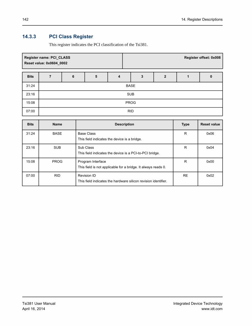
14. Register Descriptions142
14.3.3 PCI Class Register
This register indicates the PCI classification of the Tsi381.
Register name: PCI_CLASS
Reset value: 0x0604_0002
Register offset: 0x008
Bits 7 6 5 4 3 2 1 0
31:24 BASE
23:16 SUB
15:08 PROG
07:00 RID
Bits Name Description Type Reset value
31:24 BASE Base Class
This field indicates the device is a bridge.
R 0x06
23:16 SUB Sub Class
This field indicates the device is a PCI-to-PCI bridge.
R 0x04
15:08 PROG Program Interface
This field is not applicable for a bridge. It always reads 0.
R 0x00
07:00 RID Revision ID
This field indicates the hardware silicon revision identifier.
RE 0x02
Tsi381 User Manual
April 16, 2014
Integrated Device Technology
www.idt.com

14. Register Descriptions 143
14.3.4 PCI Miscellaneous 0 Register
This register controls miscellaneous PCI functions, such as the latency timer value and cacheline size.
Register name: PCI_MISC0
Reset value: 0x0001_0000
Register offset: 0x00C
Bits 7 6 5 4 3 2 1 0
31:24 BISTC SBIST Reserved CCODE
23:16 H_TYPE
15:08 Reserved
07:00 CLINE
Bits Name Description Type Reset value
31 BISTC BIST Capable;
0 = Tsi381 is not BIST capable
R 0
30 SBIST Start BIST;
0 = Tsi381 is not BIST capable
R 0
29:28 Reserved Reserved R 0
27:24 CCODE Completion Code;
0 = Tsi381 is not BIST capable
R 0
23:16 H_TYPE Header Type
This field indicates the Tsi381 is a single-function bridge.
R 0x01
15:08 Reserved Reserved (Latency timer in PCI Interface) R 0
07:00 CLINE Cacheline Sizea
04 = 4 x 32-bit word (16 bytes)
08 = 8 x 32-bit word (32 bytes)
10 = 16 x 32-bit word (64 bytes)
20 = 32 x 32-bit word (128 bytes)
This field specifies the system cacheline size in units of 32-bit words. It is used by the PCI master to determine the PCI read transaction - that is, memory read, memory read line, or memory read multiple - it should generate on the PCI bus. CLINE is also used by the PCI target to decide how much data to read on the destination bus.
Note: This field is set to 0 if CLINE is programmed to a value not specified above.
a. Software programs the system cacheline size in DWORD counts. The value programmed is used by the Tsi381 for prefetching data from memory for Memory Read Line and Memory Line Multiple transactions on the primary bus interface. Software should set only one bit at anytime. If multiple bits are set, the register defaults to 0.
R/W 0x0
Tsi381 User Manual
April 16, 2014
Integrated Device Technology
www.idt.com

14. Register Descriptions144
14.3.5 PCI Base Address Register 0
BAR0 decodes the MSI capability registers into PCI memory-mapped space. The host processor will provide access to a 4-KB memory region for memory accesses to offsets 0x80, 0x84, 0x88, 0x8C, 0x90, and 0x94. Accesses to other address offsets in this range will result in the generation of an Unsupported Request error. Depending on the setting of the UR bit in the “PCIe Uncorrectable Error Severity Register”, a FATAL error message may be generated to the host.
Register name: PCI_BAR0
Reset value: 0x0000_0000
Register offset: 0x010
Bits 7 6 5 4 3 2 1 0
31:24 ADDH
23:16 ADDH
15:08 ADDH ADDL
07:00 ADDL PREFETCH
TYPE SI
Bits Name Description Type Reset value
31:12 ADDH Higher BAR address bits
Software writes these bits to indicate where it wants the 4-KB address space to be allocated.
R/W 0x0000
11:4 ADDL Lower BAR address bits
These bits are set to 0 and are read-only to indicate a 4-KB address allocation for the MSI registers.
R 0x000
3 PREFETCH Prefetchable space
0 = Window is not prefetchable
R 0
2:1 TYPE Type
0 = Locate anywhere in 32-bit address space
R 00
0 SI Space Indicator
0 = Memory space
R 0
Tsi381 User Manual
April 16, 2014
Integrated Device Technology
www.idt.com

14. Register Descriptions 145
14.3.6 PCI Bus Number Register
Register name: PCI_BUSNUM
Reset value: Undefined
Register offset: 0x018
Bits 7 6 5 4 3 2 1 0
31:24 S_LTIMER S_LTIMER_8
23:16 SUB_BUS_NUM
15:08 S_BUS_NUM
07:00 P_BUS_NUM
Bits Name Description Type Reset value
31:27 S_LTIMER Secondary Latency Timer
This value is used by the Tsi381 to perform burst transfers on the PCI Interface. The lower 3 bits are hardwired to 0 so that the timer is limited to 8-cycle granularity.
This field defines the minimum amount of time in PCI clock cycles that the Tsi381 can retain ownership as a bus master on the PCI Interface.
00000 = PCI reset value
R/W Undefined
26:24 S_LTIMER_8 Set to 000 to force 8-cycle increments for the Secondary Latency Timer.
R 000
23:16 SUB_BUS_NUM Subordinate Bus Number
The system software programs this field with the Tsi381’s highest-numbered downstream secondary bus number. This value is used by the Tsi381 to respond to Type 1 Configuration transactions on the primary bus interface.
R/W 0x00
15:08 S_BUS_NUM Secondary Bus Number
The system software programs this field with the number of the bridge’s immediate downstream secondary bus. This value is used by the Tsi381 to convert Type 1 Configuration transactions received on its primary bus interface to Type 0 Configuration transactions.
R/W 0x00
07:00 P_BUS_NUM[7:0] Primary Bus Number
The system software writes to this field with the primary bus number of the Tsi381.
R/W 0x00
Tsi381 User Manual
April 16, 2014
Integrated Device Technology
www.idt.com

14. Register Descriptions146
14.3.7 PCI Secondary Status and I/O Limit and Base Register
Register name: PCI_MISC1_P
Reset value: 0x02A0_0101
Register offset: 0x01C
Bits 7 6 5 4 3 2 1 0
31:24 D_PE S_SERR R_MA R_TA S_TA DEVSEL MDP_D
23:16 TFBBC Reserved DEV66 Reserved
15:08 IO_LA ADD_CAP1
07:00 IO_BA ADD_CAP2
Bits Name Description Type Reset value
31 D_PE Data Parity Error Detected
This bit reports the detection of an address or data parity error on the Tsi381’s PCI Interface. The Tsi381 sets this bit when it detects one of the following:
• Address parity error as a potential target
• Data parity error as a target of a write transaction
• Data parity error as a master of a read transaction
0 = Device did not detect a parity error.
1 = Device detected a parity error.
R/W1C 0
30 S_SERR Received System Error
This bit reports the assertion of PCI_SERRn on the PCI Interface.
1 = PCI_SERRn was detected on the PCI Interface.
0 = PCI_SERRn was not detected.
R/W1C 0
29 R_MA Received Master Abort
This bit reports the detection of a Master-Abort termination by the Tsi381 when it is the master of a transaction on its PCI Interface.
0 = No Master-Abort detected.
1 = Master-Abort detected on the PCI Interface.
R/W1C 0
28 R_TA Received Target Abort
This bit reports the detection of a Target-Abort termination by the Tsi381 when it is the master of a transaction on its PCI Interface.
0 = No Target-Abort detected.
1 = Target-Abort detected on the PCI Interface.
R/W1C 0
Tsi381 User Manual
April 16, 2014
Integrated Device Technology
www.idt.com

14. Register Descriptions 147
27 S_TA Signaled Target Abort
The Tsi381 sets this bit to report the signaling of Target-Abort as target of a transaction on the PCI Interface.
0 = No Target-Abort signaled.
1 = Target-Abort signaled by the Tsi381 on its PCI Interface.
R/W1C 0
26:25 DEVSEL Device Select Timing
The Tsi381 uses medium-speed decoding on its PCI Interface.
R 01
24 MDP_D Master Data Parity Error
This bit reports the detection of an uncorrectable data error by the Tsi381.
0 = No uncorrectable data error detected on the PCI Interface.
1 = Uncorrectable data error detected on the PCI Interface.
R/W1C 0
23 TFBBC Fast Back-to-Back Capability
0 = Not supported
1 = Supported
This bit is hardwired to 1 when the secondary bus interface operates in PCI mode, indicating that the bridge can decode fast back-to-back transactions when the transactions are from the same master but to different targets.
R 1
22 Reserved Reserved R 0
21 DEV66 66-MHz Capable PCI Bus
This bit is hardwired to 1, indicating that the secondary bus interface can operate at a 66-MHz clock rate.
R 1
20:16 Reserved Reserved R 00000
15:12 IO_LA[3:0] I/O Limit Address
The Tsi381 uses this field for I/O address decoding. These bits define the upper bound of the address range used by the bridge to forward an I/O transaction from one interface to the other. These 4 bits correspond to address bits <15:12>. The address bits <11:0> are assumed equal to 12’hFFF.
R/W 0x0
11:08 ADD_CAP1 Addressing Capability
The Tsi381 supports 32-bit I/O addressing.
R 0x1
07:04 IO_BA[3:0] I/O Base Address
The Tsi381 uses this field for I/O address decoding. These bits define the lower bound of address range used by the bridge to forward an I/O transaction from one interface to the other. These 4 bits correspond to address bits <15:12>. The address bits <11:0> are assumed equal to 12’h0.
R/W 0x0
03:00 ADD_CAP2 Addressing Capability
The Tsi381 supports 32-bit I/O addressing.
R 0x1
(Continued)
Bits Name Description Type Reset value
Tsi381 User Manual
April 16, 2014
Integrated Device Technology
www.idt.com

14. Register Descriptions148
14.3.8 PCI Memory Base and Limit Register
Register name: PCI_MIO_BL
Reset value: 0x0000_0000
Register offset: 0x020
Bits 7 6 5 4 3 2 1 0
31:24 LA
23:16 LA Reserved
15:08 BA
07:00 BA Reserved
Bits Name Description Type Reset value
31:20 LA Memory Limit Address
This field is used in conjunction with the Memory Base Address for forwarding memory-mapped I/O transactions. These bits define the upper bound for the memory address range. The upper 12 bits correspond to address bits <31:20> of the address range. Bits <19:0> of the address range are 0xFFFFF.
R/W 0
19:16 Reserved Reserved R 0
15:04 BA Memory Base Address
This field defines the lower bound of the address range for forwarding memory-mapped I/O transactions. These bits correspond to address bits <31:20> of the address range. The lower 20 address bits (19:0) are 20’h0.
R/W 0
03:00 Reserved Reserved R 0
Tsi381 User Manual
April 16, 2014
Integrated Device Technology
www.idt.com

14. Register Descriptions 149
14.3.9 PCI PFM Base and Limit Register
Register name: PCI_PFM_BL
Reset value: 0x0001_0001
Register offset: 0x024
Bits 7 6 5 4 3 2 1 0
31:24 LA
23:16 LA ADD_LA_64
15:08 BA
07:00 BA ADD_BA_64
Bits Name Description Type Reset value
31:20 LA Prefetchable Memory Limit Address
This field is used in conjunction with Memory Base Address for forwarding memory-mapped I/O transactions. These bits define the upper bound for the memory address range. The upper 12 bits correspond to address bits <31:20> of the address range. Bits <19:0> of the address range are 0xFFFFF.
R/W 0
19:16 ADD_LA_64 Addressing Capability — Memory Base Address
The Tsi381 supports 64-bit addressing.
R 0x1
15:04 BA Prefetchable Memory Base Address
This field defines the lower bound of the prefetchable memory address range. These bits correspond to address bits <31:20> of the Prefetchable Address range. The lower 20 address bits (19:0) are 20’h0.
R/W 0
03:00 ADD_BA_64 Addressing Capability — Memory Range Limit Address
The Tsi381 supports 64-bit addressing.
R 0x1
Tsi381 User Manual
April 16, 2014
Integrated Device Technology
www.idt.com

14. Register Descriptions150
14.3.10 PCI PFM Base Upper 32 Address Register
14.3.11 PCI PFM Limit Upper 32 Address Register
Register name: PCI_PFM_B_UPPER
Reset value: 0x0000_0000
Register offset: 0x028
Bits 7 6 5 4 3 2 1 0
31:24 BA
23:16 BA
15:08 BA
07:00 BA
Bits Name Description Type Reset value
31:00 BA Prefetchable Memory Base Upper 32-bit Address
This field is used in conjunction with BA in the “PCI PFM Base and Limit Register” to specify the lower bound of the 64-bit prefetchable address range. The 32 bits relate to address bits <63:32> of the Prefetchable Base Address bits.
R/W 0x0
Register name: PCI_PFM_L_UPPER
Reset value: 0x0000_0000
Register offset: 0x02C
Bits 7 6 5 4 3 2 1 0
31:24 LA
23:16 LA
15:08 LA
07:00 LA
Bits Name Description Type Reset value
31:00 LA Prefetchable Memory Limit Upper 32-bit Address
This field is used in conjunction with LA in the “PCI PFM Base and Limit Register” to specify the upper bound of the 64-bit prefetchable address range. The 32 bits relate to address bits <63:32> of the Prefetchable Limit Address.
R/W 0x0
Tsi381 User Manual
April 16, 2014
Integrated Device Technology
www.idt.com

14. Register Descriptions 151
14.3.12 PCI I/O Address Upper 16 Register
Register name: PCI_IO_UPPER
Reset value: 0x0000_0000
Register offset: 0x030
Bits 7 6 5 4 3 2 1 0
31:24 IO_LA
23:16 IO_LA
15:08 IO_BA
07:00 IO_BA
Bits Name Description Type Reset value
31:16 IO_LA I/O Limit Address Upper 16-bits
This field is used in conjunction with IO_LA in the “PCI Secondary Status and I/O Limit and Base Register” to define the upper bound 32-bit address range used for decoding I/O transactions from the PCIe Interface to the PCI Interface. These bits relate to address bits <31:16> of I/O Limit Address.
R/W 0x0000
15:00 IO_BA I/O Base Address Upper 16-bits
This field is used in conjunction with IO_BA in the “PCI Secondary Status and I/O Limit and Base Register” to define the lower bound 32-bit address range used for decoding I/O transaction from the PCIe Interface to the PCI Interface. These bits relate to address bits <31:16> of I/O Base Address.
R/W 0x0000
Tsi381 User Manual
April 16, 2014
Integrated Device Technology
www.idt.com

14. Register Descriptions152
14.3.13 PCI Capability Pointer Register
Register name: PCI_CAP
Reset value: 0x0000_0080
Register offset: 0x034
Bits 7 6 5 4 3 2 1 0
31:24 Reserved
23:16 Reserved
15:08 Reserved
07:00 CAP_PTR
Bits Name Description Type Reset value
31:08 Reserved Reserved R 0x0
07:00 CAP_PTR Capabilities Pointer
This register contains the head pointer for the capability list in the PCI configuration space (see “MSI Capability and Message Control Register”).
R 0x080
Tsi381 User Manual
April 16, 2014
Integrated Device Technology
www.idt.com

14. Register Descriptions 153
14.3.14 PCI Bridge Control and Interrupt Register
Register name: PCI_MISC2
Reset value: 0x0000_00FF
Register offset: 0x03C
Bits 7 6 5 4 3 2 1 0
31:24 Reserved DISCARD_SERR
DISCARD_STAT
DISCARD2 DISCARD1
23:16 S_FPTP_EN
S_RESET MA_ERR VGA_16BIT_EN
VGA_EN ISA_EN SERR_EN S_PERESP
15:08 INT_PIN
07:00 INT_LINE
Bits Name Description Type Reset value
31:28 Reserved Reserved R 0x0
27 DISCARD_SERR Discard Timer SERR# Enable
This bit only applies in PCI mode. It enables the Tsi381 to generate either an ERR_NONFATAL (by default) or ERR_FATAL transaction on the PCIe Interface when the Secondary Discard Timer expires and a Delayed Transaction is discarded from a queue in the bridge. The severity is selectable only if Advanced Error Reporting is supported.
0 = Do not generate ERR_NONFATAL or ERR_FATAL on the PCIe Interface as a result of the expiration of the Secondary Discard Timer. Note that an error message can still be sent if Advanced Error Reporting is supported and the Delayed Transaction Discard Timer Expired Mask bit is clear.
1 = Generate ERR_NONFATAL or ERR_FATAL on the PCIe Interface if the Secondary Discard Timer expires and a Delayed Transaction is discarded from a queue in the bridge.
R/W 0
26 DISCARD_STAT Discard Timer Status
It is set to 1 when the Secondary Discard Timer expires and a Delayed Completion is discarded from a queue in the bridge.
0 = No discard timer error
1 = Discard timer error
R/W1C 0
Tsi381 User Manual
April 16, 2014
Integrated Device Technology
www.idt.com

14. Register Descriptions154
25 DISCARD2 Secondary Discard Timer
This bit determines the number of PCI clocks that the bridge waits for a master on the PCI Interface to repeat a Delayed Transaction request. The counter starts once the Completion (PCIe Completion associated with the Delayed Transaction Request) has reached the head of the downstream queue of the bridge (that is, all ordering requirements have been satisfied and the bridge is ready to complete the Delayed Transaction with the originating master on the secondary bus). If the originating master does not repeat the transaction before the counter expires, the bridge deletes the Delayed Transaction from its queue and sets the Discard Timer Status bit.
0 = Secondary Discard Timer counts 215 PCI clock cycles
1 = Secondary Discard Timer counts 210 PCI clock cycles
R/W 0
24 DISCARD1 Primary Discard Timer
This bit does not apply to PCIe. It always reads 0.
R 0
23 S_FPTP_EN Fast Back-to-Back Enable
The Tsi381 cannot generate fast back-to-back transactions as a master on the PCI Interface.
R 0
22 S_RESET Secondary Bus Reset
This bit forces the assertion of PCI_RST# on the PCI Interface. The secondary PCI_RST# is asserted by the bridge whenever this bit is set. The bridge’s secondary bus interface and any buffers between the two interfaces (primary and secondary) must be initialized back to their default state whenever this bit is set. The primary bus interface and all configuration space registers must not be affected by the setting of this bit. Because PCI_RST# is asserted for as long as this bit is set, software must observe proper PCI reset timing requirements.
0 = Do not force the assertion of the PCI Interface PCI_RST#.
1 = Force the assertion of the PCI Interface PCI_RST#.
R/W 0
(Continued)
Bits Name Description Type Reset value
Tsi381 User Manual
April 16, 2014
Integrated Device Technology
www.idt.com

14. Register Descriptions 155
21 MA_ERR Master-Abort Mode
This bit controls the behavior of a bridge when it receives a Master-Abort termination (for example, an Unsupported Request on PCIe) on either interface.
0 = Do not report Master-Aborts. When a UR response is received from PCIe for non-posted transactions, and when the secondary side is operating in PCI mode, return 0xFFFF_FFFF on reads and complete I/O writes normally. When a Master-Abort is received on the PCI Interface for posted transactions initiated from the PCIe Interface, no action is taken (that is, all data is discarded).
1 = Report UR Completions from PCIe by signaling Target-Abort on the PCI Interface when the PCI Interface is operating in PCI mode. For posted transactions initiated from the PCIe Interface and Master-Aborted on the PCI Interface, the bridge must return an ERR_NONFATAL (by default) or ERR_FATAL transaction (provided the SERR# Enable bit is set in the Command register). The severity is selectable only if Advanced Error Reporting is supported.
R/W 0
20 VGA_16BIT_EN VGA 16-Bit Enable
This bit enables the bridge to provide 16-bit decoding of VGA I/O address precluding the decoding of alias addresses every 1 KB. This bit has meaning only if VGA Enable bit is set.
1 = Executes 16-bit address decodes on VGA I/O accesses
0 = Executes 10-bit address decodes on VGA I/O accesses
R/W 0
(Continued)
Bits Name Description Type Reset value
Tsi381 User Manual
April 16, 2014
Integrated Device Technology
www.idt.com

14. Register Descriptions156
19 VGA_EN VGA Enable
This bit modifies the response of the bridge to VGA-compatible addresses. If this bit is set, the bridge forwards the following accesses on the PCIe Interface to the PCI Interface (and, conversely, block the forwarding of these addresses from the secondary interface to the PCIe Interface):
• Memory accesses in the range 0x000A_0000 to 000B_FFFF
• I/O addresses in the first 64 Kbytes of the I/O address space (Address[31:16] for PCIe are 0x0000) and where Address[9:0] is in the range of 0x3B0 to 0x3BB or 0x3C0 to 0x3DF (inclusive of ISA address aliases - Address[15:10] may possess any value and is not used in the decoding)
If this bit is set, the forwarding of VGA addresses is independent of the following:
• The value of the ISA Enable bit
• The I/O address range and memory address ranges defined by the I/O Base and Limit registers, the Memory Base and Limit registers, and the Prefetchable Memory Base and Limit registers of the bridge
The forwarding of VGA addresses is qualified by the I/O Enable and Memory Enable bits in the “PCI Control and Status Register”.
0 = Do not forward VGA compatible memory and I/O addresses from PCIe to the PCI (addresses defined above) unless they are enabled for forwarding by the defined I/O and memory address ranges.
1 = Forward VGA compatible memory and I/O addresses (addresses defined above) from PCIe to PCI (if the I/O Enable and Memory Enable bits are set) independent of the I/O and memory address ranges, and independent of the ISA Enable bit.
R/W 0
(Continued)
Bits Name Description Type Reset value
Tsi381 User Manual
April 16, 2014
Integrated Device Technology
www.idt.com
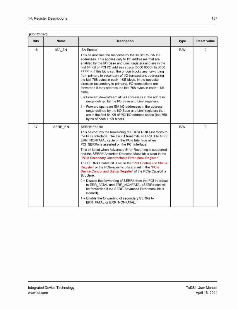
14. Register Descriptions 157
18 ISA_EN ISA Enable
This bit modifies the response by the Tsi381 to ISA I/O addresses. This applies only to I/O addresses that are enabled by the I/O Base and Limit registers and are in the first 64 KB of PCI I/O address space (0000 0000h to 0000 FFFFh). If this bit is set, the bridge blocks any forwarding from primary to secondary of I/O transactions addressing the last 768 bytes in each 1-KB block. In the opposite direction (secondary to primary), I/O transactions are forwarded if they address the last 768 bytes in each 1-KB block.
0 = Forward downstream all I/O addresses in the address range defined by the I/O Base and Limit registers.
1 = Forward upstream ISA I/O addresses in the address range defined by the I/O Base and Limit registers that are in the first 64 KB of PCI I/O address space (top 768 bytes of each 1-KB block).
R/W 0
17 SERR_EN SERR# Enable
This bit controls the forwarding of PCI SERR# assertions to the PCIe Interface. The Tsi381 transmits an ERR_FATAL or ERR_NONFATAL cycle on the PCIe Interface when PCI_SERRn is asserted on the PCI Interface.
This bit is set when Advanced Error Reporting is supported and the SERR# Assertion Detected Mask bit is clear in the “PCIe Secondary Uncorrectable Error Mask Register”.
The SERR# Enable bit is set in the “PCI Control and Status Register” or the PCIe-specific bits are set in the “PCIe Device Control and Status Register” of the PCIe Capability Structure.
0 = Disable the forwarding of SERR# from the PCI Interface to ERR_FATAL and ERR_NONFATAL (SERR# can still be forwarded if the SERR Advanced Error mask bit is cleared).
1 = Enable the forwarding of secondary SERR# to ERR_FATAL or ERR_NONFATAL.
R/W 0
(Continued)
Bits Name Description Type Reset value
Tsi381 User Manual
April 16, 2014
Integrated Device Technology
www.idt.com
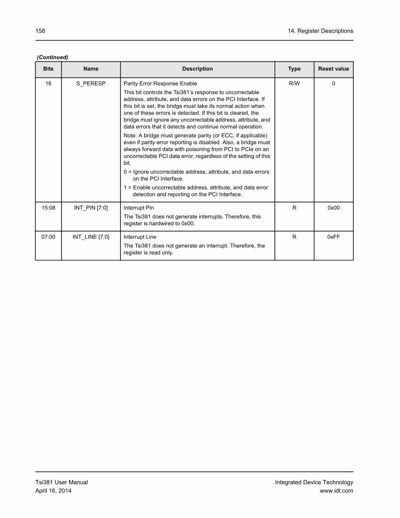
14. Register Descriptions158
16 S_PERESP Parity Error Response Enable
This bit controls the Tsi381’s response to uncorrectable address, attribute, and data errors on the PCI Interface. If this bit is set, the bridge must take its normal action when one of these errors is detected. If this bit is cleared, the bridge must ignore any uncorrectable address, attribute, and data errors that it detects and continue normal operation.
Note: A bridge must generate parity (or ECC, if applicable) even if parity error reporting is disabled. Also, a bridge must always forward data with poisoning from PCI to PCIe on an uncorrectable PCI data error, regardless of the setting of this bit.
0 = Ignore uncorrectable address, attribute, and data errors on the PCI Interface.
1 = Enable uncorrectable address, attribute, and data error detection and reporting on the PCI Interface.
R/W 0
15:08 INT_PIN [7:0] Interrupt Pin
The Tsi381 does not generate interrupts. Therefore, this register is hardwired to 0x00.
R 0x00
07:00 INT_LINE [7:0] Interrupt Line
The Tsi381 does not generate an interrupt. Therefore, the register is read only.
R 0xFF
(Continued)
Bits Name Description Type Reset value
Tsi381 User Manual
April 16, 2014
Integrated Device Technology
www.idt.com

14. Register Descriptions 159
14.3.15 Secondary Retry Count Register
Register name: SEC_RETRY_CNT
Reset value: 0x0000_0000
Register offset: 0x040
Bits 7 6 5 4 3 2 1 0
31:24 Reserved
23:16 Reserved
15:8 Reserved
7:0 Reserved SEC_RT_CNT
Bits Name Description Type Reset value
31:4 Reserved Reserved R 0
3:0 SEC_RT_CNT This field defines the number of retries that the Tsi381 will receive on the secondary bus for a requested transaction, before its internal retry counter expires. When the counter expires, the bridge discards the request.
0000 = Counting disabled (No expiration)
0001 = 256 retries before expiration
0010 = 64K retries before expiration
0100 = 16M retries before expiration
1000 = 2G retries before expiration
R/W 0000
Tsi381 User Manual
April 16, 2014
Integrated Device Technology
www.idt.com

14. Register Descriptions160
14.3.16 PCI Miscellaneous Control and Status Register
Register name: PCI_MISC_CSR
Reset value: 0x7D10_1900
Register offset: 0x044
Bits 7 6 5 4 3 2 1 0
31:24 Reserved EN_ARB EN_ARB3 EN_ARB2 EN_ARB1 EN_ARB0 Reserved P_ERR
23:16 STC_EN Reserved ARB_PRI ARB_PRI3 ARB_PRI2 ARB_PRI1 ARB_PRI0
15:08 Reserved CPL_INIT_COUNT CFG_RT
07:00 Reserved
Bits Name Description Type Reset value
31 Reserved Reserved R 0
30 EN_ARB Enable Internal Arbiter
This bit enables arbitration for Tsi381 requests.
0 = Tsi381 disables internal requests.
1 = Tsi381 enables internal requests. 0
R/W 1
29 EN_ARB3 Enable Arbiter 3
0 = Tsi381 disables PCI_REQ3n for arbitration.
1 = The bridge enables PCI_REQ3n for arbitration.
R/W 1
28 EN_ARB2 Enable Arbiter 2
0 = Tsi381 disables PCI_REQ2# for arbitration.
1 = Tsi381 enables PCI_REQ2# for arbitration.
R/W 1
27 EN_ARB1 Enable Arbiter 1
0 = Tsi381 disables PCI_REQ1# for arbitration.
1 = Tsi381 enables PCI_REQ1# for arbitration.
R/W 1
26 EN_ARB0 Enable Arbiter 0
0 = Tsi381 disables PCI_REQ0# for arbitration.
1 = Tsi381 enables PCI_REQ0# for arbitration.
R/W 1
25 Reserved Reserved R 0
24 P_ERR Parity Error Behavior
This bit controls the behavior of the Tsi381 when it detects a data parity error during a non-posted write transaction.
0 = PCI_PERRn is asserted and the corrupted data is passed.
1 = PCI_PERRn is asserted and the transaction is asserted on the originating bus, appropriate status bits are set, data is discarded, and the request is not enqueued.
R 1
Tsi381 User Manual
April 16, 2014
Integrated Device Technology
www.idt.com

14. Register Descriptions 161
23 STC_EN Short-term Caching Enable
0 = Disable short-term caching
1 = Enable short-term caching
R/W 0
22:21 Reserved Reserved R 00
20 ARB_PRI Internal Arbiter Priority
This bit sets priority for Tsi381 requests.
0 = Internal requests from the Tsi381 are assigned low priority
1 = Internal requests from the Tsi381 are assigned high priority
R/W 1
19 ARB_PRI3 Arbiter Priority 3
0 = Tsi381 assigns low priority to PCI_REQ3#.
1 = Tsi381 assigns high priority to PCI_REQ3#.
R/W 0
18 ARB_PRI2 Arbiter Priority 2
0 = Tsi381 assigns low priority to PCI_REQ2#.
1 = Tsi381 assigns high priority to PCI_REQ2#.
R/W 0
17 ARB_PRI1 Arbiter Priority 1
0 = Tsi381 assigns low priority to PCI_REQ1#.
1 = Tsi381 assigns high priority to PCI_REQ1#.
R/W 0
16 ARB_PRI0 Arbiter Priority 0
0 = Tsi381 assigns low priority to PCI_REQ0#.
1 = Tsi381 assigns high priority to PCI_REQ0#.
R/W 0
15 Reserved Reserved R 0
14:11 CPL_INIT_COUNT This is applicable for upstream Non-Posted requests in PCI mode. It indicates the number of Dwords of response data to be accumulated before starting the data transfer.
0000 = 8 Dwords
0001 = 16 Dwords
0010 = 24 Dwords
0011 = 32 Dwords
0100 = 40 Dwords
0101 = 48 Dwords
0110 = 56 Dwords
0111 = 64 Dwords
1000 = 72 Dwords
1001 = 80 Dwords
1010 = 88 Dwords
R/W 0011
(Continued)
Bits Name Description Type Reset value
Tsi381 User Manual
April 16, 2014
Integrated Device Technology
www.idt.com

14. Register Descriptions162
10:08 CFG_RT Configuration Retry Timer
The Tsi381 returns the Completion with CRS completion status for the received Type 1 configuration requests if this timer is expired before receiving the Completion from the targeted secondary device.
000 = 25 us
001 = 40 us
010 = 50 us
011 = 100 us
100 = 200 us
101 = 500 us
110 = 1 ms
111 = 10 ms
R/W 001
07:00 Reserved Reserved R 0x00
(Continued)
Bits Name Description Type Reset value
Tsi381 User Manual
April 16, 2014
Integrated Device Technology
www.idt.com

14. Register Descriptions 163
14.3.17 PCI Miscellaneous Clock Straps Register
Register name: PCI_MISC_CLK_STRAPS
Reset value: 0x0000_0100
Register offset: 0x048
Bits 7 6 5 4 3 2 1 0
31:24 Reserved
23:16 Reserved
15:08 Reserved CSR_SEL_400
07:00 Reserved OP_MODE CS_MODE
Bits Name Description Type Reset value
31:9 Reserved Reserved R 0
8 CSR_SEL_400 This bit programs the PLL clock.
1 = PLL Clock is 400 MHz. This generates 50/50% nominal PCI_CLKO.
0 = PLL Clock is 200 MHz. This generates 33/66% nominal PCI_CLKO.
Note: For normal operation, leave this bit in its default state.
R/W 1
7:4 Reserved Reserved R 0
3 OP_MODE Operating Mode
0 = Tsi381 provides the clock on PCI_CLKO with the speed defined by the M66_EN signal (33/66 MHz)
1 = Tsi381 provides the clock on PCI_CLKO with the speed defined by the CS_MODE bits. (25/33/50/60 MHz)
R/W 0
2:0 CS_MODE Clock Speed Mode
This field defines the clock speed when OP_MODE is set to 1 according to the following code points:
0bX00 = 25-MHz PCI mode
0bX01 = 33-MHz PCI mode
0bX10 = 50-MHz PCI mode
0bX11 = 66-MHz PCI mode
R/W 000
Tsi381 User Manual
April 16, 2014
Integrated Device Technology
www.idt.com

14. Register Descriptions164
14.3.18 Upstream Posted Write Threshold Register
Register name: UPST_PWR_THRES
Reset value: 0x0000_0307
Register offset: 0x04C
Bits 7 6 5 4 3 2 1 0
31:24 Reserved
23:16 Reserved
15:8 Reserved MAX_BUF_ALOC
7:0 Reserved UPST_PWR_THRES
Bits Name Description Type Reset value
31:10 Reserved Reserved. R 0
9:8 MAX_BUF_ALOC Maximum Buffer Allocation
This field determines the maximum completion buffer allocation that a single, upstream non-posted read request will create.The amount of completion buffer allocated is the MIN of these bits and the read request.
11 = 1024 bytes
10 = 512 bytes
01 = 256 bytes
00 = 128 bytes
R/W 11
7:5 Reserved Reserved. R 0
4:0 UPST_PWR_THRES This field defines the threshold for the upstream posted writes, and indicates the length of posted write data to be accumulated in the upstream posted buffer that triggers forwarding of a posted request onto the PCIe core.
Note: Other events may also trigger forwarding. For more information, see “Upstream Posted Buffer”.
This field is defined as follows:
00000 = 16 bytes
00001 = 32 bytes
00010 = 48 bytes
00011 = 64 bytes
00100 = 80 bytes
00101 = 96 bytes
00110 = 112 bytes
00111 = 128 bytes
R/W 00111
Tsi381 User Manual
April 16, 2014
Integrated Device Technology
www.idt.com
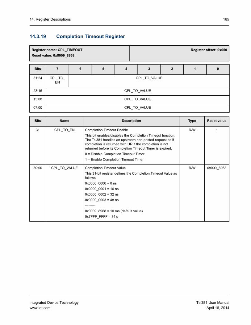
14. Register Descriptions 165
14.3.19 Completion Timeout Register
Register name: CPL_TIMEOUT
Reset value: 0x8009_8968
Register offset: 0x050
Bits 7 6 5 4 3 2 1 0
31:24 CPL_TO_EN
CPL_TO_VALUE
23:16 CPL_TO_VALUE
15:08 CPL_TO_VALUE
07:00 CPL_TO_VALUE
Bits Name Description Type Reset value
31 CPL_TO_EN Completion Timeout Enable
This bit enables/disables the Completion Timeout function. The Tsi381 handles an upstream non-posted request as if completion is returned with UR if the completion is not returned before its Completion Timeout Timer is expired.
0 = Disable Completion Timeout Timer
1 = Enable Completion Timeout Timer
R/W 1
30:00 CPL_TO_VALUE Completion Timeout Value
This 31-bit register defines the Completion Timeout Value as follows:
0x0000_0000 = 0 ns
0x0000_0001 = 16 ns
0x0000_0002 = 32 ns
0x0000_0003 = 48 ns
---------
0x0009_8968 = 10 ms (default value)
0x7FFF_FFFF = 34 s
R/W 0x009_8968
Tsi381 User Manual
April 16, 2014
Integrated Device Technology
www.idt.com

14. Register Descriptions166
14.3.20 Clock Out Enable Function and Debug Register
Register name: CLKOUT_ENB_FUNC_DBG
Reset value: 0x0000_0300
Register offset: 0x054
Bits 7 6 5 4 3 2 1 0
31:24 Reserved
23:16 Reserved
15:08 Reserved CLKOUT_ENB
07:00 Reserved FUNC_DBG
Bits Name Description Type Reset value
31:13 Reserved Reserved. R 0
12:08 CLKOUT_ENB This field enables and disables the two clocks (PCI_CLK_OUT[1:0]) supplied to the PCI secondary devices.
CLKOUT_ENB[0]
0 = Disable PCI_CLK_OUT[0]
1 = Enable PCI_CLK_OUT[0]
CLKOUT_ENB[1]
0 = Disable PCI_CLK_OUT[1]
1 = Enable PCI_CLK_OUT[1]
Note: CLKOUT_ENB[2:4] are reserved.
R/W 00011
07:02 Reserved Reserved R 0
01:00 FUNC_DBG These bits are for functional testing.
01 = Disable scrambling functionality
All other combinations are reserved.
R/W 0
Tsi381 User Manual
April 16, 2014
Integrated Device Technology
www.idt.com

14. Register Descriptions 167
14.3.21 SERRDIS_OPQEN_DTC Register
Register name: SERRDIS_OPQEN_DTC
Reset value: 0x0000_0100
Register offset: 0x058
Bits 7 6 5 4 3 2 1 0
31:24 Reserved
23:16 Reserved
15:08 Reserved ST_DIST_EN
Reserved SEC_DIST_EN
07:00 Reserved OPQ_MEM_EN
Reserved
Bits Name Description Type Reset value
31:11 Reserved Reserved R 0
10 ST_DIST_EN Short Term Discard Timer Enable
0 = Secondary discard timer value sets to either 0x03FF (1K PCI clock cycles) or 0x7FFF (32 K PCI clock cycles)
1 = Secondary discard timer value sets to 0x003F (64 PCI clock cycles)
R/W 0
9 Reserved Reserved R 0
8 SEC_DIST_EN Secondary Discard Timer Enable
0 = Disable Secondary Discard Timer
1 = Enable Secondary Discard Timer
R/W 1
07:06 Reserved Reserved R 0
5 OPQ_MEM_EN Opaque Memory Address Enable
0 = Disable opaque range in memory address space.
1 = Enable opaque range in memory address space. Requests that fall in this range are handled with Unsupported Requests on primary interface and Master-Abort on secondary interface.
R/W 0
4:0 Reserved Reserved R 0
Tsi381 User Manual
April 16, 2014
Integrated Device Technology
www.idt.com

14. Register Descriptions168
14.4 Opaque Addressing RegistersThe Opaque address range is defined in the memory address space. Any memory transaction hitting this range is not claimed by the Tsi381. Base and limit values are programmed in following device-specific registers. Opaque addressing decoding enabled by setting OPQ_MEM_EN to 1 in the “SERRDIS_OPQEN_DTC Register”.
14.4.1 Opaque Memory Lower Register
Register name: PCI_OPQMEMB_OPQMEML
Reset value: 0x0001_0001
Register offset: 0x05C
Bits 7 6 5 4 3 2 1 0
31:24 OPQ_LL
23:16 OPQ_LL OPQ_LL64
15:08 OPQ_LB
07:00 OPQ_LB OPQ_LB64
Bits Name Description Type Reset value
31:20 OPQ_LL Opaque memory lower limit. R/W 0
19:16 OPQ_LL64 Opaque memory lower limit.
Set to 0x1 to indicate support for 64-bit addressing.
R 1
15:04 OPQ_LB Opaque memory lower base. R/W 0
03:00 OPQ_LB64 Opaque memory lower base.
Set to 0x1 to indicate support for 64-bit addressing.
R 1
Tsi381 User Manual
April 16, 2014
Integrated Device Technology
www.idt.com

14. Register Descriptions 169
14.4.2 Opaque Memory Upper Base Register
14.4.3 Opaque Memory Upper Limit Register
Register name: PCI_OPQMEMBUP
Reset value: 0x0000_0000
Register offset: 0x060
Bits 7 6 5 4 3 2 1 0
31:24 OPQ_UB
23:16 OPQ_UB
15:08 OPQ_UB
07:00 OPQ_UB
Bits Name Description Type Reset value
31:00 OPQ_UB Opaque memory upper base. R/W 0x0
Register name: PCI_OPQMEMLUP
Reset value: 0x0000_0000
Register offset: 0x064
Bits 7 6 5 4 3 2 1 0
31:24 OPQ_UL
23:16 OPQ_UL
15:08 OPQ_UL
07:00 OPQ_UL
Bits Name Description Type Reset value
31:00 OPQ_UL Opaque memory upper limit. R/W 0x0
Tsi381 User Manual
April 16, 2014
Integrated Device Technology
www.idt.com

14. Register Descriptions170
14.5 Upstream Non-transparent Address Remapping RegistersThe Tsi381 supports address remapping, which is one of the requirements of non-transparent bridging. All transactions that fall in the non-transparent address range are mapped to different address locations according to following device-specific registers.
14.5.1 NTMA Control Register
Register name: NTMA_CTRL
Reset value: 0x0000_0000
Register offset: 0x068
Bits 7 6 5 4 3 2 1 0
31:24 NTMA_LBA
23:16 NTMA_LBA Reserved
15:08 Reserved
07:00 Reserved NTMA_RMP
Reserved
Bits Name Description Type Reset value
31:20 NTMA_LBA NTMA primary lower base address. R/W 0x0
19:04 Reserved Reserved R 0x0
03 NTMA_RMP 0 = Disable NTMA address remapping.
1 = Enable NTMA address remapping.
R/W 0x0
02:00 Reserved Reserved R 0x0
Tsi381 User Manual
April 16, 2014
Integrated Device Technology
www.idt.com
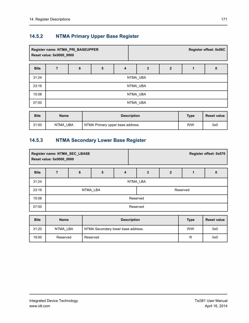
14. Register Descriptions 171
14.5.2 NTMA Primary Upper Base Register
14.5.3 NTMA Secondary Lower Base Register
Register name: NTMA_PRI_BASEUPPER
Reset value: 0x0000_0000
Register offset: 0x06C
Bits 7 6 5 4 3 2 1 0
31:24 NTMA_UBA
23:16 NTMA_UBA
15:08 NTMA_UBA
07:00 NTMA_UBA
Bits Name Description Type Reset value
31:00 NTMA_UBA NTMA Primary upper base address. R/W 0x0
Register name: NTMA_SEC_LBASE
Reset value: 0x0000_0000
Register offset: 0x070
Bits 7 6 5 4 3 2 1 0
31:24 NTMA_LBA
23:16 NTMA_LBA Reserved
15:08 Reserved
07:00 Reserved
Bits Name Description Type Reset value
31:20 NTMA_LBA NTMA Secondary lower base address. R/W 0x0
19:00 Reserved Reserved R 0x0
Tsi381 User Manual
April 16, 2014
Integrated Device Technology
www.idt.com

14. Register Descriptions172
14.5.4 NTMA Secondary Upper Base Register
14.5.5 NTMA Secondary Lower Limit Register
Register name: NTMA_SEC_BASEUPPER
Reset value: 0x0000_0000
Register offset: 0x074
Bits 7 6 5 4 3 2 1 0
31:24 NTMA_UBA
23:16 NTMA_UBA
15:08 NTMA_UBA
07:00 NTMA_UBA
Bits Name Description Type Reset value
31:00 NTMA_UBA NTMA Secondary upper base address. R/W 0x0
Register name: NTMA_SEC_LOWER_LIMIT
Reset value: 0x0000_0000
Register offset: 0x078
Bits 7 6 5 4 3 2 1 0
31:24 NTMA_LLA
23:16 NTMA_LLA Reserved
15:08 Reserved
07:00 Reserved
Bits Name Description Type Reset value
31:20 NTMA_LLA NTMA Secondary lower limit address. R/W 0x0
19:00 Reserved Reserved R 0x0
Tsi381 User Manual
April 16, 2014
Integrated Device Technology
www.idt.com

14. Register Descriptions 173
14.5.6 NTMA Secondary Upper Limit Register
14.6 PCI Capability RegistersThe Tsi381 device supports PCI and PCIe extended capabilities options. The Capabilities Pointer field in the “PCI Capability Pointer Register” (0x034) points to the first PCI capabilities option, while the first PCIe extended capability option is always located at 0x100 (see “PCIe Advanced Error Reporting Capability Register”).
Register name: NTMA_SEC_UPPER_LIMIT
Reset value: 0x0000_0000
Register offset: 0x07C
Bits 7 6 5 4 3 2 1 0
31:24 NTMA_ULA
23:16 NTMA_ULA
15:08 NTMA_ULA
07:00 NTMA_ULA
Bits Name Description Type Reset value
31:00 NTMA_ULA NTMA Secondary Upper limit address. R/W 0x0
Tsi381 User Manual
April 16, 2014
Integrated Device Technology
www.idt.com

14. Register Descriptions174
14.6.1 MSI Capability and Message Control Register
Register name: MSI_CAP_PNTR
Reset value: 0x0186_A005
Register offset: 0x080
Bits 7 6 5 4 3 2 1 0
31:24 Reserved PVM
23:16 ADD64 MME MMC MSIE
15:08 NXT_PTR
07:00 CAP_ID
Bits Name Description Type Reset value
31:25 Reserved Reserved R 0x0
24 PVM Per Vector Masking
0 = The function does not support per-vector masking
1 = The function supports MSI per-vector masking
R 0x1
23 ADD64 64-bit Message Address
0 = The function cannot send a 64-bit message address
1 = The function can send a 64-bit message address
R 0x1
22:20 MME Multiple Message Enable
System software writes to this field to indicate the number of allocated vectors (equal to or less than the number of requested vectors). The number of allocated vectors is aligned to a power of two. The encoding is defined as:
000 = 1 vectors allocated
001 = 2 vectors allocated
010 = 4 vectors allocated
011 = 8 vectors allocated
100-111 = Reserved
R/W 0x0
Tsi381 User Manual
April 16, 2014
Integrated Device Technology
www.idt.com
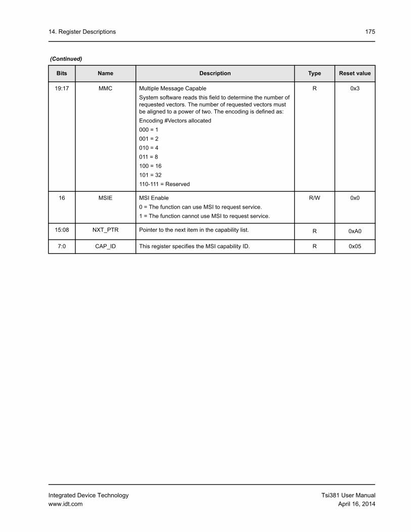
14. Register Descriptions 175
19:17 MMC Multiple Message Capable
System software reads this field to determine the number of requested vectors. The number of requested vectors must be aligned to a power of two. The encoding is defined as:
Encoding #Vectors allocated
000 = 1
001 = 2
010 = 4
011 = 8
100 = 16
101 = 32
110-111 = Reserved
R 0x3
16 MSIE MSI Enable
0 = The function can use MSI to request service.
1 = The function cannot use MSI to request service.
R/W 0x0
15:08 NXT_PTR Pointer to the next item in the capability list. R 0xA0
7:0 CAP_ID This register specifies the MSI capability ID. R 0x05
(Continued)
Bits Name Description Type Reset value
Tsi381 User Manual
April 16, 2014
Integrated Device Technology
www.idt.com

14. Register Descriptions176
14.6.2 MSI Message Address Register
Register name: MSI_MSG_ADDR
Reset value: 0x0000_0000
Register offset: 0x084
Bits 7 6 5 4 3 2 1 0
31:24 MSI_ADDR
23:16 MSI_ADDR
15:08 MSI_ADDR
07:00 MSI_ADDR Reserved
Bits Name Description Type Reset value
31:2 MSI_ADDR MSI Message Address
System specified message address. If the message enable bit is set (MSIE in “MSI Capability and Message Control Register”), the contents of this register specify the DWORD-aligned address for the MSI memory write transaction. Address bits 1 and 0 are driven zero during the address phase.
R/W 0
1:0 Reserved Reserved R 00
Tsi381 User Manual
April 16, 2014
Integrated Device Technology
www.idt.com

14. Register Descriptions 177
14.6.3 MSI Message Address Upper Register
14.6.4 MSI Message Data Register
Register name: MSI_MSG_UPP_ADDR
Reset value: 0x0000_0000
Register offset: 0x088
Bits 7 6 5 4 3 2 1 0
31:24 MSI_UPP_ADDR
23:16 MSI_UPP_ADDR
15:08 MSI_UPP_ADDR
07:00 MSI_UPP_ADDR
Bits Name Description Type Reset value
31:00 MSI_UPP_ADDR MSI Message Upper Address
System-specified message upper address. If the message enable bit is set (MSIE in “MSI Capability and Message Control Register”), the contents of this register (if non-zero) specify the upper 32 bits of a 64-bit message address (AD[63:32]).
If the contents of this register are zero, the function uses the 32-bit address specified by the “MSI Capability and Message Control Register”.
R/W 0
Register name: MSI_MSG_DATA
Reset value: 0x0000_0000
Register offset: 0x08C
Bits 7 6 5 4 3 2 1 0
31:24 Reserved
23:16 Reserved
15:08 MSI_DATA
07:00 MSI_DATA
Bits Name Description Type Reset value
31:16 Reserved Reserved R 0
Tsi381 User Manual
April 16, 2014
Integrated Device Technology
www.idt.com

14. Register Descriptions178
15:00 MSI_DATA System-specified Message Data
This is the data that is sent upstream as a posted write when an MSI occurs.
The Multiple Message Enable field (MME in “MSI Capability and Message Control Register”) defines the number of low order message data bits the function is permitted to modify to generate its system software allocated vectors.
If 8 vectors are granted, the message data or vector is as follows (the “Y” data comes from the MSI_DATA field).
GPIO = MSI0
GPI1 = MSI1
GPI2 = MSI2
GPI3 = MSI3
INTA = MSI4
INTB = MSI5
INTC = MSI6
INTD = MSI7
1. MSI0 = 0bYYYY Y000
2. MSI1 = 0bYYYY Y001
3. MSI2 = 0bYYYY Y010
6. …
7. MSI7 = 0bYYYY Y111
If 4 vectors are granted the message data or vector is as follows.
1. MSI0 or MSI4 = 0bYYYY YY00
2. MSI1 or MSI5 = 0bYYYY YY01
3. MSI2 or MSI6 = 0bYYYY YY10
4. MSI3 or MSI7 = 0bYYYY YY11
If 2 vectors are granted the message data or vector is as follows.
1. MSI0/2/4/6 = 0bYYYY YYY0
2. MSI1/3/5/7 = 0bYYYY YYY1
If 1 vector is allocated the MSI_DATA is not modified.
R/W 0x0000
(Continued)
Bits Name Description Type Reset value
Tsi381 User Manual
April 16, 2014
Integrated Device Technology
www.idt.com

14. Register Descriptions 179
14.6.5 MSI Mask Register
Register name: MSI_MASK_BITS
Reset value: 0x0000_0000
Register offset: 0x090
Bits 7 6 5 4 3 2 1 0
31:24 Reserved
23:16 Reserved
15:08 Reserved
07:00 MSI_MASK_BITS
Bits Name Description Type Reset value
31:8 Reserved Reserved R 0
7:0 MSI_MASK_BITS For each Mask bit that is set, the function is prohibited from sending the associated message.
Bit 0 = MSI0
Bit 1 = MSI1
...
Bit 7 = MSI7
R/W 0x00
Tsi381 User Manual
April 16, 2014
Integrated Device Technology
www.idt.com

14. Register Descriptions180
14.6.6 MSI Pending Register
Register name: MSI_PENDING_BITS
Reset value: 0x0000_0000
Register offset: 0x094
Bits 7 6 5 4 3 2 1 0
31:24 Reserved
23:16 Reserved
15:08 Reserved
07:00 MSI_PENDING_BITS
Bits Name Description Type Reset value
31:8 Reserved Reserved R 0
7:0 MSI_PENDING_BITS
For each Pending bit that is set, the function has a pending message associated with it.
Bit 0 = MSI0
Bit 1 = MSI1
...
Bit 7 = MSI7
R 0x00
Tsi381 User Manual
April 16, 2014
Integrated Device Technology
www.idt.com

14. Register Descriptions 181
14.6.7 PCI Power Management Capability Register
This register defines bytes 0 to 3 of the power management capability option.
Register name: PCI_PMC
Reset value: 0x7803_C001
Register offset: 0x0A0
Bits 7 6 5 4 3 2 1 0
31:24 PME_SUP D2_SP D1_SP AUX_CUR
23:16 AUX_CUR DSI Reserved PME_CK PM_VER
15:08 NXT_PTR
07:00 CAP_ID
Bits Name Description Type Reset value
31:27 PME_SUP PME Support
This field indicates the power management states from which the Tsi381 device can indicate PME#.
The value reported by this field is based on Serial EEPROM programming that indicates how auxiliary power is routed to the Tsi381 device in the system.
Given the right power supplies, the Tsi381 can assert the PME# signals in D3COLD.
In the absence of Serial EEPROM information, the Tsi381 will report PME support for power levels down to D3HOT.
RE 01111
26 D2_SP D2 Support
This field always returns 0 since the Tsi381 does not support the D2 power management state.
R 0
25 D1_SP D1 Support
This field always returns 0 since the Tsi381 does not support the D1 power management state.
R 0
24:22 AUX_CUR Aux Current
This field returns a value 0 indicating the device is self powered.
R 000
21 DSI Device Specific Initialization
Hardwired to 0. No special initialization is required.
R 0
20 Reserved Reserved. It always reads 0. R 0
19 PME_CK PME Clock
This field is not applicable to devices with a PCIe Interface. It always reads 0.
R 0
Tsi381 User Manual
April 16, 2014
Integrated Device Technology
www.idt.com

14. Register Descriptions182
18:16 PM_VER Version
This field indicates a version number of 011 indicating it supports the PCI Bus Power Management Interface Specification (Revision 1.2).
R 011
15:8 NXT_PTR Next Pointer
This field points to the next capability option: “PCIe Capabilities Register” (0x0C0).
R 0xC0
7:0 CAP_ID Capability ID
This field contains the value 0x01 indicating a power management capability option.
R 0x01
(Continued)
Bits Name Description Type Reset value
Tsi381 User Manual
April 16, 2014
Integrated Device Technology
www.idt.com

14. Register Descriptions 183
14.6.8 PCI Power Management Control and Status Register
This register defines the control and status registers of the power management capability option.
Register name: PCI_PMCS
Reset value: 0x0000_0008
Register offset: 0x0A4
Bits 7 6 5 4 3 2 1 0
31:24 DATA
23:16 Reserved
15:08 PME_ST DATA_SC DATA_SEL PME_EN
07:00 Reserved NO_SOFT_RST
Reserved PWR_ST
Bits Name Description Type Reset value
31:24 DATA Power Data
The Tsi381 does not support the Power Data field.
R 0x00
23:16 Reserved Reserved. It always reads 0. R 0x0
15 PME_ST Power PME Status
This field indicates whether this device can generate PME#. This field’s value is independent of whether the Power PME Enable field is set to 1.
0 = No PME# is being asserted by this PCI function.
1 = A PME# status is reported by this PCI function. If PME_EN is also set to 1, this PCI function is also asserting the PME# signal. Writing 1 to this field clears the field.
Note: The Tsi381 does not support this feature; this bit always returns a 0.
R 0
14:13 DATA_SC Power Data Scale
This field always returns 0 since the Tsi381 device does not support the DATA field.
R 00
12:9 DATA_SEL Power Data Select
This field always returns 0 since the Tsi381 device does not support the DATA field.
R 0x0
Tsi381 User Manual
April 16, 2014
Integrated Device Technology
www.idt.com

14. Register Descriptions184
8 PME_EN Power PME Enable
This field enables PME# assertion. The initial value of this field depends on whether the device woke from power-off or D3COLD.
• From power-off, this field starts disabled.
• From D3COLD, this field contains the enable condition going into the D3COLD state.
0 = Disable PME# generation.
1 = Enable PME# generation.
R/W 0
7:4 Reserved Reserved 1. It always reads 0. R 0x0
3 NO_SOFT_RST Power No Soft Reset
This field indicates whether the device needs a soft reset after transitioning from D3HOT to D0. This field always returns 1 indicating a soft reset is not required.
R 1
2 Reserved Power Reserved 0. It always reads 0. R 0
1:0 PWR_ST Power State
This field determines the current power state of the PCI function, and sets a new state. If the new state is not supported, the change is ignored.
00 = D0
01 = D1
10 = D2
11 = D3HOT
R/W 0
(Continued)
Bits Name Description Type Reset value
Tsi381 User Manual
April 16, 2014
Integrated Device Technology
www.idt.com

14. Register Descriptions 185
14.6.9 EEPROM Control Register
Register name: EE_CTRL
Reset value: Undefined
Register offset: 0x0AC
Bits 7 6 5 4 3 2 1 0
31:24 Reserved CMD ADD_WIDTH BUSY CMD_VLD
23:16 ADD
15:08 ADD
07:00 DATA
Bits Name Description Type Reset value
31:30 Reserved Reserved R 0x0
29:28 CMD Command
01 = Read
10 = Write
R/W 0x0
27:26 ADD_WIDTH Address width
This field indicates the address width of the serial EEPROM, and whether or not an EEPROM device is present.
00 = No EEPROM
01 = 9-bit address
10 = 16-bit address
Note: A blank EEPROM is indicated with 0b00. If this occurs, these bits must be written with the appropriate values before the EEPROM can be accessed.
R/W Undefined
25 BUSY This bit indicates the serial EEPROM is busy with Read/Write operation.
Software must poll this bit before initiating a write/read to the external EEPROM through a configuration write to the “EEPROM Control Register”. For information on software polling, see “System Diagram”.
R 0x0
24 CMD_VLD This bit validates the command and side-band signals to the serial EEPROM.
R/W 0x0
23:08 ADD Address
This is the EEPROM address to be read from or written into.
R/W 0x0000
07:00 DATA DATA
This is the data to be written into the EEPROM.
R/W 0x00
Tsi381 User Manual
April 16, 2014
Integrated Device Technology
www.idt.com

14. Register Descriptions186
14.6.10 Secondary Bus Device Mask Register
This register provides a method to support private devices on the PCI bus. The process of converting Type 1 configuration transactions to Type 0 configuration transactions is modified by the contents of this register. A configuration transaction that targets a device masked by this register is rerouted to device 15. Setting this register to all zeros disables device masking.
Register name: SBUS_DEVMSK
Reset value: 0x0000_0000
Register offset: 0x0B0
Bits 7 6 5 4 3 2 1 0
31:24 Reserved DEVMSK_13
Reserved DEVMSK_9 Reserved
23:16 DEVMSK_7 DEVMSK_6 DEVMSK_5 DEVMSK_4 Reserved DEVMSK_1 Reserved
15:08 Reserved
07:00 Reserved
Bits Name Description Type Reset Value
31:30 Reserved Reserved R 0
29 DEVMSK_13 Device Mask 13
0 = Rerouting disabled for device 13.
1 = Block assertion of PCI_AD (Pin 29) for configuration transactions to device 13, assert pin PCI_AD (Pin 31) instead.
R/W 0
28:26 Reserved Reserved. Masking for devices 12, 11, and 10 is not implemented. Operation of the Tsi381 is unaffected by the value of these bits.
R 0
25 DEVMSK_9 Device Mask 9
0 = Rerouting disabled for device 9.
1 = Block assertion of PCI_AD (Pin 25) for configuration transactions to device 9, assert pin PCI_AD (Pin 31) instead.
R/W 0
24 Reserved Reserved. Masking for device 8 is not implemented. Operation of the Tsi381 is unaffected by the value of this bit.
R 0
23 DEVMSK_7 Device Mask 7
0 = Rerouting disabled for device 7.
1 = Block assertion of PCI_AD (Pin 23) for configuration transactions to device 7, assert pin PCI_AD (Pin 31) instead.
R/W 0
Tsi381 User Manual
April 16, 2014
Integrated Device Technology
www.idt.com

14. Register Descriptions 187
22 DEVMSK_6 Device Mask 6
0 = Rerouting disabled for device 6.
1 = Block assertion of PCI_AD (Pin 22) for configuration transactions to device 6, assert pin PCI_AD (Pin 31) instead.
R/W 0
21 DEVMSK_5 Device Mask 5
0 = Rerouting disabled for device 5.
1 = Block assertion of PCI_AD (Pin 21) for configuration transactions to device 5, assert pin PCI_AD (Pin 31) instead.
R/W 0
20 DEVMSK_4 Device Mask 4
0 = Rerouting disabled for device 4.
1 = Block assertion of PCI_AD (Pin 20) for configuration transactions to device 4, assert pin PCI_AD (Pin 31) instead.
R/W 0
19:18 Reserved Reserved. Masking for devices 3 and 2 is not implemented. Operation of the Tsi381 is unaffected by the value of these bits.
R 0
17 DEVMSK_1 Device Mask 1
0 = Rerouting disabled for device 1.
1 = Block assertion of PCI_AD (Pin 17) for configuration transactions to device 1, assert pin PCI_AD (Pin 31) instead.
R/W 0
16:0 Reserved Reserved. Operation of the Tsi381 is unaffected by the value of these bits.
R 0
(Continued)
Bits Name Description Type Reset Value
Tsi381 User Manual
April 16, 2014
Integrated Device Technology
www.idt.com
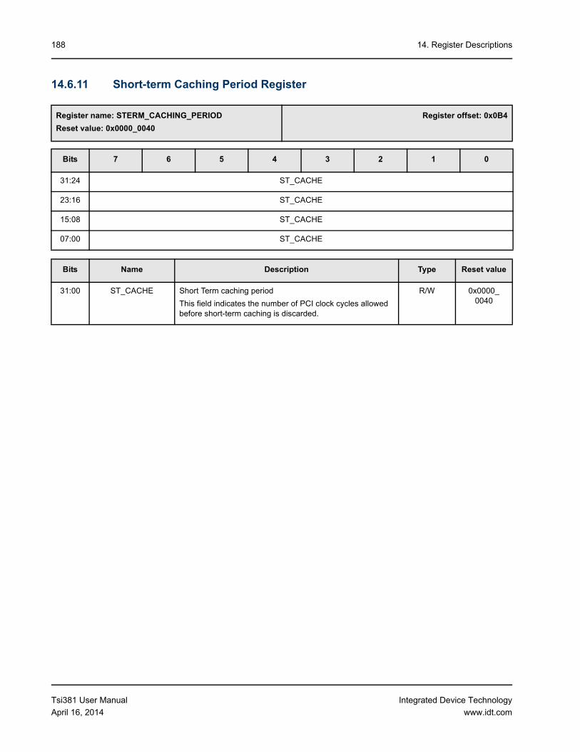
14. Register Descriptions188
14.6.11 Short-term Caching Period Register
Register name: STERM_CACHING_PERIOD
Reset value: 0x0000_0040
Register offset: 0x0B4
Bits 7 6 5 4 3 2 1 0
31:24 ST_CACHE
23:16 ST_CACHE
15:08 ST_CACHE
07:00 ST_CACHE
Bits Name Description Type Reset value
31:00 ST_CACHE Short Term caching period
This field indicates the number of PCI clock cycles allowed before short-term caching is discarded.
R/W 0x0000_0040
Tsi381 User Manual
April 16, 2014
Integrated Device Technology
www.idt.com

14. Register Descriptions 189
14.6.12 Retry Timer Status Register
Register name: TIMER_STATUS
Reset value: 0x0000_0000
Register offset: 0x0B8
Bits 7 6 5 4 3 2 1 0
31:24 Reserved
23:16 Reserved
15:08 Reserved
07:00 Reserved SEC_DIS_STAT
Reserved SEC_R_STAT
Bits Name Description Type Reset value
31:03 Reserved Reserved R 0x0
2 SEC_DIS_STAT Secondary Discard Timer status
For more information on this timer, see DISCARD2 in “PCI Bridge Control and Interrupt Register”.
0 = Secondary discard timer has not expired.
1 = Secondary discard timer has expired.
R 0
1 Reserved Reserved R 0
0 SEC_R_STAT Secondary Retry timer status
For more information on this timer, see “Secondary Retry Count Register”.
0 = Secondary retry timer has not expired
1 = Secondary retry timer has expired
R 0
Tsi381 User Manual
April 16, 2014
Integrated Device Technology
www.idt.com

14. Register Descriptions190
14.6.13 Prefetch Control Register
Register name: PREF_CTRL
Reset value: 0x0300_0041
Register offset: 0x0BC
Bits 7 6 5 4 3 2 1 0
31:24 Reserved P_MR P_MRL P_MRM
23:16 MRL_66 MRL_33
15:08 MRL_33 MRM_66
07:00 MRM_66 MRM_33
Bits Name Description Type Reset value
31:27 Reserved Reserved R 0x00
26 P_MR 0 = The Tsi381 fetches a Dword of data in case of 32-bit PCI data bus mode.
1 = The Tsi381 prefetches as per the value specified in MRL_66/MRL_33 fields on behalf of the PCI master for memory read command.
R/W 0
25 P_MRL 0 = The Tsi381 prefetches one cacheline of data.
1 = The Tsi381 prefetches as per the value specified in MRL_66/MRL_33 fields on behalf of the PCI master for memory read line command.
R/W 1
24 P_MRM 0 = The Tsi381 prefetches two cachelines of data.
1 = The Tsi381 prefetches as per the value specified in MRM_66/MRM_33 fields on behalf of PCI master for memory read multiple command.
R/W 1
23:18 MRL_66 This bit indicates the threshold parameter for Memory read line and memory read commands in 66-MHz PCI mode. Unit is 64-byte chunk.
6’h00 = 64 bytes
6’h01 = 128 bytes
...
6’h3F = 4096 bytes
R/W 0x00
17:12 MRL_33 This bit indicates the threshold parameter for Memory read line and memory read commands in 33-MHz PCI mode. Unit is 64-byte chunk.
6’h00 = 64 bytes
6’h01 = 128 bytes
...
6’h3F = 4096 bytes
R/W 0x00
Tsi381 User Manual
April 16, 2014
Integrated Device Technology
www.idt.com

14. Register Descriptions 191
14.7 PCIe Capability RegistersIn the Tsi381, the PCIe capability is located in PCI 2.3 configuration space at 0x0C0 and contains 20 bytes.
11:6 MRM_66 This bit indicates the threshold parameter for Memory read multiple command in 66-MHz PCI mode. Unit is 64-byte chunk.
6’h00 = 64 bytes
6’h01 = 128 bytes
...
6’h3F = 4096 bytes
R/W 0x01
5:0 MRM_33 This bit indicates the threshold parameter for Memory read multiple command in 33-MHz PCI mode. Unit is 64-byte chunk.
6’h00 = 64 bytes
6’h01 = 128 bytes
...
6’h3F = 4096 bytes
R/W 0x01
(Continued)
Bits Name Description Type Reset value
Tsi381 User Manual
April 16, 2014
Integrated Device Technology
www.idt.com

14. Register Descriptions192
14.7.1 PCIe Capabilities Register
The PCIe capabilities register defines bytes 0 to 3 of the PCIe capability option.
Register name: PCIE_CAP
Reset value: 0x0071_0010
Register offset: 0x0C0
Bits 7 6 5 4 3 2 1 0
31:24 Reserved INT_MN SLOT_IMP
23:16 DP_TYPE CAP_VER
15:08 NXT_PTR
07:00 CAP_ID
Bits Name Description Type Reset value
31:30 Reserved PCIe Reserved. It always reads 0. R 00
29:25 INT_MN PCIe Interrupt Message Number
The Tsi381 device does not have slot status or root port status. It always reads 0.
R 00000
24 SLOT_IMP PCIe Slot Implemented
This field is not applicable for a bridge device. It always reads 0.
R 0
23:20 DP_TYPE PCIe Device Port Type
This field indicates the device is a PCIe bridge device.
R 0111
19:16 CAP_VER PCIe Capability Version
This field returns a version number of 1 indicating it supports PCIe 1.1 capabilities.
R 0001
15:08 NXT_PTR Next Pointer
This field points to the next capability option. In the Tsi381, this will contain a value of 0x00 indicating there are no more PCI compatible capabilities options.
R 0x00
07:00 CAP_ID Capability ID
This field contains the value 0x10 indicating a PCIe capability option.
R 0x10
Tsi381 User Manual
April 16, 2014
Integrated Device Technology
www.idt.com

14. Register Descriptions 193
14.7.2 PCIe Device Capabilities Register
This register defines bytes 4 to 7 of the PCIe capability option.
Register name: PCIE_DEV_CAP
Reset value: 0x0000_8000
Register offset: 0x0C4
Bits 7 6 5 4 3 2 1 0
31:24 Reserved PL_SCL PL_VAL
23:16 PL_VAL Reserved
15:08 ROL_BAS_ERR_REP
Reserved L1_LAT L0S_LAT
07:00 L0S_LAT EXT_TAG PH_FUNC MAX_SIZE
Bits Name Description Type Reset value
31:28 Reserved PCIE Reserved. It always reads 0. R 0000
27:26 PL_SCL PCIe Captured Slot Power Limit Scale
This field specifies the scale used for the Slot Power Limit Value.
00 = 1.0x
01 = 0.1x
10 = 0.01x
11 = 0.001x
This value is set by the Set_Slot_Power_Limit Message. The default value is 00.
R 00
25:18 PL_VAL PCIe Captured Slot Power Limit Value
In combination with the Slot Power Limit Scale value, this field specifies the upper limit on power supplied by the slot. Power limit (in Watts) calculated by multiplying the value in this field by the value in the Slot Power Limit Scale field. This value is set by the Set_Slot_Power_Limit Message. The default value is 0x00.
R 0x00
17:16 Reserved PCIe Reserved. It always reads 0. R 000
15 ROL_BAS_ERR_REP
Role-based Error Reporting
This bit, when set, indicates that the device uses the functionality defined in the Error Reporting ECN for the PCIe Base Specification, (Revision 1.0a), and later incorporated into the PCI Express Base Specification (Revision 1.1). This bit must be set by all devices conforming to the ECN, PCIe 1.1 Specification, or subsequent PCIe Base Specification revisions.
R 1
Tsi381 User Manual
April 16, 2014
Integrated Device Technology
www.idt.com

14. Register Descriptions194
14:12 Reserved The Value read from these bits is 0b000. Previous version of the PCI specification had defined theses bits, they are now defined as read only, and return 0b000.
System software is permitted to write any value to these bits.
R 000
11:9 L1_LAT PCIe Endpoint L1 Acceptable Latency
This field always returns 0 since the Tsi381 does not support the L1 ASPM state.
R 000
8:6 L0S_LAT PCIe Endpoint L0s Acceptable Latency
This field indicates the acceptable latency for transition from L0s to L0 state. This field is set to 0b000 since the Tsi381 is not an endpoint.
R 000
5 EXT_TAG PCIe Extended Tag Field Supported
This field contains the value 0 indicating 5-bit tag fields are supported.
R 0
4:3 PH_FUNC PCIe Phantom Functions Supported
This field is 0 indicating no phantom functions are used.
R 00
2:0 MAX_SIZE PCIe Maximum Payload Size Supported
000 = 128 bytes
R 000
(Continued)
Bits Name Description Type Reset value
Tsi381 User Manual
April 16, 2014
Integrated Device Technology
www.idt.com

14. Register Descriptions 195
14.7.3 PCIe Device Control and Status Register
This register defines bytes 8 to 11 of the PCIe capability option.
Register name: PCIE_DEV_CSR
Reset value: 0x0000_2000
Register offset: 0x0C8
Bits 7 6 5 4 3 2 1 0
31:24 Reserved
23:16 Reserved TRAN_PND
AUX_PWR_DTD
UNS_REQ_DTD
FTL_ERR_DTD
NFTL_ERR_DTD
COR_ERR_DTD
15:08 CFG_RETRY_EN
MAX_RD_SIZE EN_SNP_NREQ
AUX_PWR_PM_EN
PHN_EN EXT_TAG_EN
07:00 MAX_PAY_SIZE EN_RLX_ORD
UNS_REQ_EN
FTL_ERR_EN
NFTL_ERR_EN
COR_ERR_EN
Bits Name Description Type Reset value
31:22 Reserved PCIe Reserved. It always reads 0. R 0x000
21 TRAN_PND PCIe Transaction Pending
This field indicates the Tsi381 issued Non-Posted Requests that have not been completed.
0 = No pending completion of Non-Posted Requests.
1 = Pending completion of Non-Posted Requests.
R 0
20 AUX_PWR_DTD PCIe Aux Power Detected
This field indicates whether the Tsi381 detected AUX power. The Tsi381, however, does not require the Auxiliary Power.
0 = No Aux power detected.
1 = Aux power detected.
R 0
19 UNS_REQ_DTD PCIe Unsupported Request Detected
This field indicates whether an unsupported request was detected.
0 = No error detected.
1 = Error detected. Writing 1 clears this error.
R/W1C 0
18 FTL_ERR_DTD PCIe Fatal Error Detected
This field indicates whether a fatal error was detected.
0 = No error detected.
1 = Error detected. Writing 1 clears this error.
R/W1C 0
Tsi381 User Manual
April 16, 2014
Integrated Device Technology
www.idt.com

14. Register Descriptions196
17 NFTL_ERR_DTD PCIe Non-Fatal Error Detected
This field indicates whether a non-fatal error was detected.
0 = No error detected.
1 = Error detected. Writing 1 clears this error.
R/W1C 0
16 COR_ERR_DTD PCIe Correctable Error Detected
This field indicates whether a correctable error was detected.
0 = No error detected.
1 = Error detected. Writing 1 clears this error.
R/W1C 0
15 CFG_RETRY_EN Bridge Configuration Retry Enable
0 = Disable the Tsi381 to return Configuration Request Retry Status (CRS) in response to Configuration Requests to the target devices below the bridge.
1 = Enable the Tsi381 to return Configuration Request Retry Status (CRS) in response to Configuration Requests to the target devices below the bridge.
R/W 0
14:12 MAX_RD_SIZE PCIe Max Read Request Size
This field sets the maximum read request size for the Tsi381 as a requestor.
000 = 128 bytes
001 = 256 bytes
010 = 512 bytes
011 = 1024 bytes
100 = 2048 bytes
101 = 4096 bytes
110-111 = Reserved.
R/W 010
11 EN_SNP_NREQ PCIe Enable Snoop Not Required
The Tsi381 does not set the No Snoop attribute. This bit is hardwired to 0.
R 0
10 AUX_PWR_PM_EN
PCIe Aux Power PM Enable
When this bit is set the Tsi381 can draw AUX power independent of PME AUX power.
0 = Do not allow use of AUX power other than PME AUX.
1 = Allow use of AUX power other than PME AUX.
R/W 0
9 PHN_EN PCIe Phantom Functions Enable
The Tsi381 does not use phantom functions. This bit always returns 0.
R 0
8 EXT_TAG_EN PCIe Extended Tag Field Enable
The Tsi381 does not support extended tag fields. This bit always returns 0.
R 0
(Continued)
Bits Name Description Type Reset value
Tsi381 User Manual
April 16, 2014
Integrated Device Technology
www.idt.com

14. Register Descriptions 197
7:5 MAX_PAY_SIZE PCIe Maximum Payload Size
This field indicates the maximum payload size that can be used for data transmission by the Tsi381. This must be a subset of the size reported by MAX_SIZE in “PCIe Device Capabilities Register”.
000-111 = 128 bytes
R/W 000
4 EN_RLX_ORD PCIe Enable Relaxed Ordering
This field controls whether relaxed ordering for transactions is enabled.
0 = Relaxed ordering is disabled.
1 = Relaxed ordering is enabled.
R 0
3 UNS_REQ_EN PCIe Unsupported Request Reporting Enable
This field controls reporting of unsupported requests.
0 = No error reporting.
1 = Error reporting enabled.
R/W 0
2 FTL_ERR_EN PCIe Fatal Error Reporting Enable
This bit, in conjunction with other bits, controls sending ERR_FATAL messages (for more information, see Figure 20).
0 = No error reporting.
1 = Error reporting enabled.
R/W 0
1 NFTL_ERR_EN PCIe Non-Fatal Error Reporting Enable
This bit, in conjunction with other bits, controls sending ERR_NONFATAL messages (for more information, see Figure 20).
0 = No error reporting.
1 = Error reporting enabled.
R/W 0
0 COR_ERR_EN PCIe Correctable Error Reporting Enable
This bit, in conjunction with other bits, controls sending ERR_COR messages (for more information, see Figure 20).
0 = No error reporting.
1 = Error reporting enabled.
R/W 0
(Continued)
Bits Name Description Type Reset value
Tsi381 User Manual
April 16, 2014
Integrated Device Technology
www.idt.com

14. Register Descriptions198
14.7.4 PCIe Link Capabilities Register
Register name: PCIE_LNK_CAP
Reset value: 0x0000_3411
Register offset: 0x0CC
Bits 7 6 5 4 3 2 1 0
31:24 PORT_NUM
23:16 Reserved DLL_LNK_ACT_REP_
CAP
SRP_DWN_ERR_REP
_CAP
CLK_PWR_MGT
L1_EXIT
15:08 L1_EXIT L0S_EXIT ASPM MAX_WIDTH
07:00 MAX_WIDTH MAX_SPEED
Bits Name Description Type Reset value
31:24 PORT_NUM PCIe Port Number
The Tsi381 always reports a port number of 0 for this field.
R 0x00
23:21 Reserved PCIe Reserved. This field always reads 0. R 0x00
20 DLL_LNK_ACT_REP_CAP
Data Link Layer Link Active Reporting Capable
For a downstream port, this bit must be set to 1 if the component can report the DL_Active state of the Data Link Control and Management State Machine. For a hot-plug capable downstream port, this bit must be set to 1.
For upstream ports and components that do not support this capability, this bit must be hardwired to 0.
Note: The Tsi381 does not support DLL_LNK_ACT_REP_CAP. This field always reads 0.
R 0
19 SRP_DWN_ERR_REP_CAP
Surprise Down Error Reporting Capable
For a downstream port, this bit must be set to 1 if the component can detect and report a Surprise Down error condition.
For upstream ports and components that do not support this capability, this bit must be hardwired to 0.
Note: The Tsi381 does not support SRP_DWN_ERR_REP_CAP. This field always reads 0.
R 0
Tsi381 User Manual
April 16, 2014
Integrated Device Technology
www.idt.com

14. Register Descriptions 199
18 CLK_PWR_MGT Clock Power Management
0 = The component does not have this capability, and the reference clock(s) must not be removed in these link states.
1 = The component tolerates the removal of any reference clock(s) via the “clock request” (CLKREQ#) mechanism when the link is in the L1 and L2/3 Ready link states.
This capability is applicable only in form factors that support “clock request” (CLKREQ#) capability.
For a multifunction device, each function indicates its capability independently. Power Management configuration software must only permit reference clock removal if all functions of the multifunction device indicates a 1 in this bit.
Note: The Tsi381 does not support CLK_PWR_MGT. This field always reads 0.
R 0
17:15 L1_EXIT PCIe L1 Exit Latency
The Tsi381 does not support the L1 ASPM state. This field always returns 0.
RE 000
14:12 L0S_EXIT PCIe L0s Exit Latency
The Tsi381 L0s exit latency will be as 256-512ns which will be reported as 0b011. This value can be overwritten by the serial EEPROM.
000 = Less than 64 ns
001 = 64 ns to less than 128 ns
010 = 128 ns to less than 256 ns
011 = 256 ns to less than 512 ns
100 = 512 ns to less than 1 us
101= 1 us to less than 2us
110 = 2-4 us
111 = More than 4 us
RE 011
11:10 ASPM PCIe ASPM Support
The Tsi381 supports only the L0s ASPM state. This field always returns 1.
R 01
09:04 MAX_WIDTH PCIe Maximum Link Width
This field indicates the maximum number of PCIe lanes that can be used for communicating with the Tsi381.
0x01 = 1 PCIe lane
R 0x01
03:00 MAX_SPEED PCIe Maximum Link Speed
This field is always 1 indicating a 2.5-Gbps link.
R 0x1
(Continued)
Bits Name Description Type Reset value
Tsi381 User Manual
April 16, 2014
Integrated Device Technology
www.idt.com

14. Register Descriptions200
14.7.5 PCIe Link Control Register
This register defines bytes 16 to 17 of the PCIe capability option.
Register name: PCIE_LNK_CSR
Reset value: 0x0011_0000
Register offset: 0x0D0
Bits 7 6 5 4 3 2 1 0
31:24 Reserved DLL_LNK_ACT
SLT_CLK_CONFIG
Reserved NEG_LNK_WIDTH
23:16 NEG_LNK_WIDTH LNK_SPEED
15:08 Reserved
07:00 E_SYNC COM_CLK RETRAIN LNK_DIS RCB Reserved ASPM_CTL
Bits Name Description Type Reset value
31:30 Reserved Reserved R 00
29 DLL_LNK_ACT Data Link Layer Active. This bit indicates the status of the Data Link Control and Management State Machine. This bit is hardwired to 0.
R 0
28 SLT_CLK_CONFIG Slot Clock Configuration. This bit indicates the Tsi381 uses the same physical reference clock that the platform provides on the connector.
This bit can be loaded from the serial EEPROM as part of the PCB configuration information.
R 0
27:26 Reserved Reserved R 0
25:20 NEG_LNK_WIDTH Negotiated Link Width. This field indicates the negotiated width of the PCIe Link.
000001 = x1 lane
R 0x01
19:16 LNK_SPEED Link Speed. This field indicates the negotiated Link Speed of the PCIe Link.
0001 = 2.5-Gbps PCIe Link
R 0x1
15:8 Reserved Reserved R 0x00
7 E_SYNC PCIe Extended Synchronization
This field is normally only used when attempting to capture the PCIe link on an analyzer since it allows the synchronization cycle to be extended allowing the analyzer to synchronize to the link.
0 = Normal operation.
1 = Enable extended synchronization
R/W 0
Tsi381 User Manual
April 16, 2014
Integrated Device Technology
www.idt.com

14. Register Descriptions 201
6 COM_CLK PCIe Common Clock Configuration
This field selects between a distributed common reference clock or an asynchronous reference clock. After setting both ends of the link to the same value, the link must be retrained from the bridge side of the link.
Components use this common clock configuration information to report the correct L0s and L1 Exit Latencies.
0 = Asynchronous reference clock
1 = Distributed common reference clock
R/W 0
5 RETRAIN PCIe Retrain Link
This field is reserved for a bridge device. It always reads 0.
R 0
4 LNK_DIS PCIe Link Disable
This field is reserved for a bridge device. It always reads 0.
R 0
3 RCB PCIe Read Completion Boundary
This field is set by system software to indicate the read completion boundary value of the upstream root port.
0 = 64 bytes
1 = 128 bytes
R/W 0
2 Reserved PCIe Reserved. It always reads 0. R 0
1:0 ASPM_CTL PCIe ASPM Control
This field enables different levels of ASPM.
00: Disabled
01 :L0s Entry enabled
10-11: = Reserved (not supported)
R/W 00
(Continued)
Bits Name Description Type Reset value
Tsi381 User Manual
April 16, 2014
Integrated Device Technology
www.idt.com

14. Register Descriptions202
14.8 Downstream Non-transparent Address Remapping Registers
14.8.1 Secondary Bus Non-prefetchable Address Remap Control Register
Register name: AR_SBNPCTRL
Reset value: 0x0000_0000
Register offset: 0x0E4
Bits 7 6 5 4 3 2 1 0
31:24 SEC_NP_LBASE
23:16 SEC_NP_LBASE Reserved
15:08 Reserved IO_SIZE
07:00 Reserved NP_REMAPP_EN
Reserved
Bits Name Description Type Reset value
31:20 SEC_NP_LBASE Secondary non-prefetchable lower base. R/W 0x000
19:13 Reserved Reserved. R 0x00
12:8 IO_SIZE This field describes how many upper bits of a downstream I/O address are discarded.
R/W 0x00
7:4 Reserved Reserved. R 0x0
3 NP_REMAPP_EN 1 = Enable non-prefetchable address remapping R/W 0x0
2:0 Reserved Reserved. R 0x0
Tsi381 User Manual
April 16, 2014
Integrated Device Technology
www.idt.com

14. Register Descriptions 203
14.8.2 Secondary Bus Non-prefetchable Upper Base Address Remap Register
14.8.3 Secondary Bus Prefetchable Address Remap Control Register
Register name: AR_SBNPBASE
Reset value: 0x0000_0000
Register offset: 0x0E8
Bits 7 6 5 4 3 2 1 0
31:24 SEC_NP_UBA
23:16 SEC_NP_UBA
15:08 SEC_NP_UBA
07:00 SEC_NP_UBA
Bits Name Description Type Reset value
31:00 SEC_NP_UBA Secondary bus non-prefetchable upper base. R/W 0x000
Register name: AR_SBPPRECTRL
Reset value: 0x0000_0000
Register offset: 0x0EC
Bits 7 6 5 4 3 2 1 0
31:24 SEC_PRE_LBA
23:16 SEC_PRE_LBA Reserved
15:08 Reserved
07:00 Reserved PRE_REMAP_EN
Reserved
Bits Name Description Type Reset value
31:20 SEC_PRE_LBA Secondary bus prefetchable lowerbase. R/W 0x000
19:4 Reserved Reserved. R 0x0000
3 PRE_REMAP_EN 0 = Disable prefetchable address remapping
1 = Enable prefetchable address remapping
R/W 0x0
2:0 Reserved Reserved. R 0x0
Tsi381 User Manual
April 16, 2014
Integrated Device Technology
www.idt.com

14. Register Descriptions204
14.8.4 Secondary Bus Prefetchable Upper Base Address Remap Register
14.8.5 Primary Bus Non-prefetchable Upper Base Address Remap Register
Register name: AR_SBPREBASEUPPER
Reset value: 0x0000_0000
Register offset: 0x0F0
Bits 7 6 5 4 3 2 1 0
31:24 SEC_PRE_UBA
23:16 SEC_PRE_UBA
15:08 SEC_PRE_UBA
07:00 SEC_PRE_UBA
Bits Name Description Type Reset value
31:00 SEC_PRE_UBA Secondary bus non-prefetchable upper base. R/W 0x000
Register name: AR_PBNPBASEUPPER
Reset value: 0x0000_0000
Register offset: 0x0F4
Bits 7 6 5 4 3 2 1 0
31:24 PRI_NP_UBA
23:16 PRI_NP_UBA
15:08 PRI_NP_UBA
07:00 PRI_NP_UBA
Bits Name Description Type Reset value
31:00 PRI_NP_UBA Primary bus non-prefetchable upper base. R/W 0x0000_0000
Tsi381 User Manual
April 16, 2014
Integrated Device Technology
www.idt.com

14. Register Descriptions 205
14.8.6 Primary Bus Non-prefetchable Upper Limit Remap Register
Register name: AR_PBNPLIMITUPPER
Reset value: 0x0000_0000
Register offset: 0x0F8
Bits 7 6 5 4 3 2 1 0
31:24 PRI_NP_ULA
23:16 PRI_NP_ULA
15:08 PRI_NP_ULA
07:00 PRI_NP_ULA
Bits Name Description Type Reset value
31:00 PRI_NP_ULA Primary bus non-prefetchable upper Limit R/W 0x0000_0000
Tsi381 User Manual
April 16, 2014
Integrated Device Technology
www.idt.com

14. Register Descriptions206
14.9 Advanced Error Reporting Capability Registers
14.9.1 PCIe Advanced Error Reporting Capability Register
Register name: PCIE_ADV_ERR_CAP
Reset value: 0x0001_0001
Register offset: 0x100
Bits 7 6 5 4 3 2 1 0
31:24 NXT_CAP_OFF
23:16 NXT_CAP_OFF CAP_VER
15:08 EXT_CAP_ID
07:00 EXT_CAP_ID
Bits Name Description Type Reset value
31:20 NXT_CAP_OFF Next Capability Offset
This field contains the offset to the next PCIe capability structure or 0x000 if no other items exist in the linked list of capabilities.
For Extended Capabilities implemented in device configuration space, this offset is relative to the beginning of PCI compatible configuration space and thus must always be either 0x000 (for terminating list of capabilities) or greater than 0x0FF.
R 0x000
19:16 CAP_VER Capability Version
This field is a PCI-SIG defined version number that indicates the version of the capability structure present.
R 0x1
15:0 EXT_CAP_ID PCIe Extended Capability ID
This field is a PCI-SIG defined ID number that indicates the function and format of the extended capability. The Extended Capability ID for the Advanced Error Reporting Capability is 0x0001.
R 0x0001
Tsi381 User Manual
April 16, 2014
Integrated Device Technology
www.idt.com

14. Register Descriptions 207
14.9.2 PCIe Uncorrectable Error Status Register
Register name: PCIE_UNC_ERR_STAT
Reset value: 0x0000_0000
Register offset: 0x104
Bits 7 6 5 4 3 2 1 0
31:24 Reserved
23:16 Reserved UR ECRC MAL_TLP RXO UXC
15:08 CA CTO FCPE PTLP Reserved
07:00 Reserved DLPE Reserved Undefined
Bits Name Description Type Reset value
31:21 Reserved Reserved R 0x000
20 UR Unsupported Request Error Status R/W1CS 0
19 ECRC ECRC Error Status R/W1CS 0
18 MAL_TLP Malformed TLP Status R/W1CS 0
17 RXO Receiver Overflow Status R/W1CS 0
16 UXC Unexpected Completion Status R/W1CS 0
15 CA Completer Abort Status R/W1CS 0
14 CTO Completion Timeout Status R/W1CS 0
13 FCPE Flow Control Protocol Error Status R/W1CS 0
12 PTLP Poisoned TLP Status R/W1CS 0
11:5 Reserved Reserved R 0x00
4 DLPE Data Link Protocol Error Status R/W1CS 0
3:1 Reserved Reserved R 000
0 Undefined Undefined R 0
Tsi381 User Manual
April 16, 2014
Integrated Device Technology
www.idt.com

14. Register Descriptions208
14.9.3 PCIe Uncorrectable Error Mask Register
Register name: PCIE_UERR_MASK
Reset value: 0x0000_0000
Register offset: 0x108
Bits 7 6 5 4 3 2 1 0
31:24 Reserved
23:16 Reserved UR ECRC MAL_TLP RXO UXC
15:08 CA CTO FCPE PTLP Reserved
07:00 Reserved DLPE Reserved Undefined
Bits Name Description Type Reset value
31:21 Reserved Reserved R 0x000
20 UR Unsupported Request Error Mask R/WS 0
19 ECRC ECRC Error Mask R/WS 0
18 MAL_TLP Malformed TLP Mask R/WS 0
17 RXO Receiver Overflow Mask R/WS 0
16 UXC Unexpected Completion Mask R/WS 0
15 CA Completer Abort Mask R/WS 0
14 CTO Completion Timeout Mask R/WS 0
13 FCPE Flow Control Protocol Error Mask R/WS 0
12 PTLP Poisoned TLP Mask R/WS 0
11:5 Reserved Reserved R 0x00
4 DLPE Data Link Protocol Error Mask R/WS 0
3:1 Reserved Reserved R 000
0 Undefined Undefined R 0
Tsi381 User Manual
April 16, 2014
Integrated Device Technology
www.idt.com

14. Register Descriptions 209
14.9.4 PCIe Uncorrectable Error Severity Register
Register name: PCIE_UNC_ERR_SEV
Reset value: 0x0006_2030
Register offset: 0x10C
Bits 7 6 5 4 3 2 1 0
31:24 Reserved
23:16 Reserved UR ECRC MAL_TLP RXO UXC
15:08 CA CTO FCPE PTLP Reserved
07:00 Reserved SDES DLPE Reserved Unused
Bits Name Description Type Reset value
31:21 Reserved Reserved R 0x000
20 UR Unsupported Request Error Severity R/WS 0
19 ECRC ECRC Error Severity R/WS 0
18 MAL_TLP Malformed TLP Severity R/WS 1
17 RXO Receiver Overflow Severity R/WS 1
16 UXC Unexpected Completion Severity
Note: In the PCI Express Base Specification (Revision 1.1), Unexpected Completions are only reported as correctable errors: this bit should not be set to 1.
R/WS 0
15 CA Completer Abort Severity R/WS 0
14 CTO Completion Timeout Severity R/WS 0
13 FCPE Flow Control Protocol Error Severity R/WS 1
12 PTLP Poisoned TLP Severity R/WS 0
11:6 Reserved Reserved R 0x00
5 SDES Surprise Down Error Severity R/WS 1
4 DLPE Data Link Protocol Error Severity R/WS 1
3:1 Reserved Reserved R 000
0 Unused Reserved
Note: Bit 0 is Training Error Status for PCIe 1.0a, but is not defined for the PCI Express Base Specification (Revision 1.1).
R 0
Tsi381 User Manual
April 16, 2014
Integrated Device Technology
www.idt.com

14. Register Descriptions210
14.9.5 PCIe Correctable Error Status Register
Register name: PCIE_COR_ERR
Reset value: 0x0000_0000
Register offset: 0x110
Bits 7 6 5 4 3 2 1 0
31:24 Reserved
23:16 Reserved
15:08 Reserved ANFE RT_TO Reserved RN_RO
07:00 B_DLLP B_TLP Reserved RXE
Bits Name Description Type Reset value
31:14 Reserved Reserved R 0x00000
13 ANFE Advisory Non-Fatal Error Status R/W1CS 0
12 RT_TO Replay Timer Timeout Status R/W1CS 0
11:9 Reserved Reserved R 000
8 RN_RO REPLAY_NUM Rollover Status R/W1CS 0
7 B_DLLP Bad DLLP Status
This bit is set to indicate the following conditions:
• Calculated CRC was not equal to received CRC.
R/W1CS 0
6 B_TLP Bad TLP Status
This bit is set to indicate the following conditions:
• Physical layer indicated errors with the TLP
• TLP ended with EDB, but calculated CRC was not the logical NOT of the received CRC
• Calculated CRC was not equal to the received CRC
R/W1CS 0
5:1 Reserved Reserved R 0x0
0 RXE Receiver Error Status R/W1CS 0
Tsi381 User Manual
April 16, 2014
Integrated Device Technology
www.idt.com

14. Register Descriptions 211
14.9.6 PCIe Correctable Error Mask Register
Register name: PCIE_COR_MASK
Reset value: 0x0000_2000
Register offset: 0x114
Bits 7 6 5 4 3 2 1 0
31:24 Reserved
23:16 Reserved
15:08 Reserved ANFE RT_TO Reserved RN_RO
07:00 B_DLLP B_TLP Reserved RXE
Bits Name Description Type Reset value
31:14 Reserved Reserved R 0x00000
13 ANFE Advisory Non-Fatal Error Mask R/WS 1
12 RT_TO Replay Timer Timeout Mask R/WS 0
11:9 Reserved Reserved R 000
8 RN_RO REPLAY_NUM Rollover Mask R/WS 0
7 B_DLLP Bad DLLP Mask R/WS 0
6 B_TLP Bad TLP Mask R/WS 0
5:1 Reserved Reserved R 0x0
0 RXE Receiver Error Mask R/WS 0
Tsi381 User Manual
April 16, 2014
Integrated Device Technology
www.idt.com

14. Register Descriptions212
14.9.7 PCIe Advanced Error Capabilities and Control Register
Register name: PCIE_ADV_ERR_CAP_CTRL
Reset value: 0x0000_00A0
Register offset: 0x118
Bits 7 6 5 4 3 2 1 0
31:24 Reserved
23:16 Reserved
15:08 Reserved EC_EN
07:00 EC_CAP EG_EN EG_CAP ERR_PTR
Bits Name Description Type Reset value
31:9 Reserved Reserved R 0x0000_00
8 EC_EN ECRC Check Enable
0 = Disable
1 = Enable
R/WS 0
7 EC_CAP ECRC Check Capable
This bit indicates the Tsi381 can check ECRC.
R 1
6 EG_EN ECRC Generation Enable
0 = Disable
1 = Enable
R/WS 0
5 EG_CAP ECRC Generation Capable
This bit indicates the Tsi381 can generate ECRC.
R 1
4:0 ERR_PTR First Error Pointer
This pointer is a read-only field that identifies the bit position of the first error reported in the “PCIe Uncorrectable Error Status Register”.
RS 0
Tsi381 User Manual
April 16, 2014
Integrated Device Technology
www.idt.com

14. Register Descriptions 213
14.9.8 PCIe Header Log 1 Register
14.9.9 PCIe Header Log 2 Register
Register name: PCIE_HL1
Reset value: 0x0000_0000
Register offset: 0x11C
Bits 7 6 5 4 3 2 1 0
31:24 HEADER[127:120]
23:16 HEADER[119:112]
15:08 HEADER[111:104]
07:00 HEADER[103:96]
Bits Name Description Type Reset value
31:00 HEADER[127:96] Header of TLP associated with error. RS 0
Register name: PCIE_HL2
Reset value: 0x0000_0000
Register offset: 0x120
Bits 7 6 5 4 3 2 1 0
31:24 HEADER[95:88]
23:16 HEADER[87:80]
15:08 HEADER[79:72]
07:00 HEADER[71:64]
Bits Name Description Type Reset value
31:00 HEADER[95:64] Header of TLP associated with error. RS 0
Tsi381 User Manual
April 16, 2014
Integrated Device Technology
www.idt.com

14. Register Descriptions214
14.9.10 PCIe Header Log 3 Register
14.9.11 PCIe Header Log 4 Register
Register name: PCIE_HL3
Reset value: 0x0000_0000
Register offset: 0x124
Bits 7 6 5 4 3 2 1 0
31:24 HEADER[63:56]
23:16 HEADER[55:48]
15:08 HEADER[47:40]
07:00 HEADER[39:32]
Bits Name Description Type Reset value
31:00 HEADER[63:32] Header of TLP associated with error. RS 0
Register name: PCIE_HL4
Reset value: 0x0000_0000
Register offset: 0x128
Bits 7 6 5 4 3 2 1 0
31:24 HEADER[31:24]
23:16 HEADER[23:16]
15:08 HEADER[15:08]
07:00 HEADER[07:00]
Bits Name Description Type Reset value
31:00 HEADER[31:00] Header of TLP associated with error. RS 0
Tsi381 User Manual
April 16, 2014
Integrated Device Technology
www.idt.com

14. Register Descriptions 215
14.9.12 PCIe Secondary Uncorrectable Error Status Register
Register name: PCIE_SEC_UERR_STAT
Reset value: 0x0000_0000
Register offset: 0x12C
Bits 7 6 5 4 3 2 1 0
31:24 Reserved
23:16 Reserved
15:08 Reserved IB_ERR SERR_AD PERR_AD DTDTE UADD_ERR
UATT_ERR
07:00 UDERR USCM USCE Reserved R_MA R_TA MA_SC TA_SC
Bits Name Description Type Reset value
31:14 Reserved Reserved R 0x0000_0
13 IB_ERR Internal Bridge Error Status (No Header Log).
The Tsi381 never sets this bit.
R 0
12 SERR_AD SERR# Assertion Detected (No Header Log) R/W1CS 0
11 PERR_AD PERR# Assertion Detected R/W1CS 0
10 DTDTE Delayed Transaction Discard Timer Expired Status (No Header Log)
R/W1CS 0
9 UADD_ERR Uncorrectable Address Error Status R/W1CS 0
8 UATT_ERR Uncorrectable Attribute Error Status R/W1CS 0
7 UDERR Uncorrectable Data Error Status R/W1CS 0
6 USCM Uncorrectable Split Completion Message Data Error Statusa
a. The Tsi381 never sets this bit since it does not support PCI-X.
R/W1CS 0
5 USCE Unexpected Split Completion Error Statusa R/W1CS 0
4 Reserved Reserved R 0
3 R_MA Received Master-Abort Status R/W1CS 0
2 R_TA Received Target-Abort Status R/W1CS 0
1 MA_SC Master-Abort on Split Completion Statusa R/W1CS 0
0 TA_SC Target-Abort on Split Completion Statusa R/W1CS 0
Tsi381 User Manual
April 16, 2014
Integrated Device Technology
www.idt.com

14. Register Descriptions216
14.9.13 PCIe Secondary Uncorrectable Error Mask Register
Register name: PCIE_SEC_UERR_MASK
Reset value: 0x0000_17A8
Register offset: 0x130
Bits 7 6 5 4 3 2 1 0
31:24 Reserved
23:16 Reserved
15:08 Reserved IB_ERR SERR_AD PERR_AD DTDTE UADD_ERR
UATT_ERR
07:00 UDERR USCM USCE Reserved R_MA R_TA MA_SC TA_SC
Bits Name Description Type Reset value
31:14 Reserved Reserved R 0x0000_0
13 IB_ERR Internal Bridge Error Mask (No Header Log) R/WS 0
12 SERR_AD SERR# Assertion Detected Mask (No Header Log) R/WS 1
11 PERR_AD PERR# Assertion Detected Mask R/WS 0
10 DTDTE Delayed Transaction Discard Timer Expired Mask (No Header Log)
R/WS 1
9 UADD_ERR Uncorrectable Address Error Mask R/WS 1
8 UATT_ERR Uncorrectable Attribute Error Mask R/WS 1
7 UDERR Uncorrectable Data Error Mask R/WS 1
6 USCM Uncorrectable Split Completion Message Data Error Maska
a. This bit has no effect on the Tsi381 since it does not support PCI-X.
R/WS 0
5 USCE Unexpected Split Completion Error Maska R/WS 1
4 Reserved Reserved R 0
3 R_MA Received Master-Abort Mask R/WS 1
2 R_TA Received Target-Abort Mask R/WS 0
1 MA_SC Master-Abort on Split Completion Maska R/WS 0
0 TA_SC Target-Abort on Split Completion Maska R/WS 0
Tsi381 User Manual
April 16, 2014
Integrated Device Technology
www.idt.com

14. Register Descriptions 217
14.9.14 PCIe Secondary Uncorrectable Error Severity Register
Register name: PCIE_SEC_UERR_SEV
Reset value: 0x0000_1340
Register offset: 0x134
Bits 7 6 5 4 3 2 1 0
31:24 Reserved
23:16 Reserved
15:08 Reserved IB_ERR SERR_AD PERR_AD DTDTE UADD_ERR
UATT_ERR
07:00 UDERR USCM USCE Reserved R_MA R_TA MA_SC TA_SC
Bits Name Description Type Reset value
31:14 Reserved Reserved R 0x0000_0
13 IB_ERR Internal Bridge Error Severity (No Header Log) R/WS 0
12 SERR_AD SERR# Assertion Detected Severity (No Header Log) R/WS 1
11 PERR_AD PERR# Assertion Detected Severity R/WS 0
10 DTDTE Delayed Transaction Discard Timer Expired Severity (No Header Log)
R/WS 0
9 UADD_ERR Uncorrectable Address Error Severity R/WS 1
8 UATT_ERR Uncorrectable Attribute Error Severity R/WS 1
7 UDERR Uncorrectable Data Error Severity R/WS 0
6 USCM Uncorrectable Split Completion Message Data Error Severitya
a. This bit has no effect on the Tsi381 since it does not support PCI-X.
R/WS 1
5 USCE Unexpected Split Completion Error Severitya R/WS 0
4 Reserved Reserved R 0
3 R_MA Received Master-Abort Severity R/WS 0
2 R_TA Received Target-Abort Severity R/WS 0
1 MA_SC Master-Abort on Split Completion Severity R/WS 0
0 TA_SC Target-Abort on Split Completion Severity R/WS 0
Tsi381 User Manual
April 16, 2014
Integrated Device Technology
www.idt.com

14. Register Descriptions218
14.9.15 PCIe Secondary Error Capabilities and Control Register
14.9.16 PCIe Secondary Header Log 1 Register
Register name: PCIE_ERR_CAP_CTRL
Reset value: 0x0000_0000
Register offset: 0x138
Bits 7 6 5 4 3 2 1 0
31:24 Reserved
23:16 Reserved
15:08 Reserved
07:00 Reserved SUFEP
Bits Name Description Type Reset value
31:05 Reserved Reserved R 0
04:00 SUFEP Secondary Uncorrectable First Error Pointer. RS 0x00
Register name: PCIE_SEC_HL1
Reset value: 0x0000_0000
Register offset: 0x13C
Bits 7 6 5 4 3 2 1 0
31:24 TRAN_ATT[31:24]
23:16 TRAN_ATT[23:16]
15:08 TRAN_ATT[15:08]
07:00 TRAN_ATT[07:00]
Bits Name Description Type Reset value
31:00 TRAN_ATT[31:00] Transaction Attribute
This field is [31:0] of the 36-bit value transferred on C/BE[3:0]# and AD[31:0] during the attribute phase.
RS 0x0
Tsi381 User Manual
April 16, 2014
Integrated Device Technology
www.idt.com

14. Register Descriptions 219
14.9.17 PCIe Secondary Header Log 2 Register
Register name: PCIE_SEC_HL2
Reset value: 0x0000_0000
Register offset: 0x140
Bits 7 6 5 4 3 2 1 0
31:24 Reserved
23:16 Reserved
15:08 Reserved TRAN_CU
07:00 TRAN_CL TRAN_ATT[35:32]
Bits Name Description Type Reset value
31:12 Reserved Reserved R 0
11:08 TRAN_CU Transaction Command Upper
This value is transferred on C/BE[3:0]# during the second address phase of a DAC transaction.
RS 0x0
07:04 TRAN_CL Transaction Command Lower
This value is transferred on C/BE[3:0]# during the first address phase.
RS 0x0
3:0 TRAN_ATT[35:32] Transaction Attribute
This field is [35:32] of the 36-bit value transferred on C/BE[3:0]# and AD[31:0] during the attribute phase.
RS 0x0
Tsi381 User Manual
April 16, 2014
Integrated Device Technology
www.idt.com

14. Register Descriptions220
14.9.18 PCIe Secondary Header Log 3 Register
14.9.19 PCIe Secondary Header Log 4 Register
Register name: PCIE_SEC_HL3
Reset value: 0x0000_0000
Register offset: 0x144
Bits 7 6 5 4 3 2 1 0
31:24 TRAN_ADD[31:24]
23:16 TRAN_ADD[23:16]
15:08 TRAN_ADD[15:08]
07:00 TRAN_ADD[07:00]
Bits Name Description Type Reset value
31:00 TRAN_ADD[31:00] Transaction Address
This is the first 32 bits of the 64-bit value transferred on AD[31:0] during the first and second address phases.
The first address phase is logged in this field, and the second address is logged in “PCIe Secondary Header Log 4 Register”.
RS 0x0
Register name: PCIE_SEC_HL4
Reset value: 0x0000_0000
Register offset: 0x148
Bits 7 6 5 4 3 2 1 0
31:24 TRAN_ADD[63:56]
23:16 TRAN_ADD[55:48]
15:08 TRAN_ADD[47:40]
07:00 TRAN_ADD[39:32]
Bits Name Description Type Reset value
31:00 TRAN_ADD[63:32] Transaction Address
This is the second 32 bits of the 64-bit value transferred on AD[31:0] during the first and second address phases.
The first address phase is logged in “PCIe Secondary Header Log 3 Register”, and the second address phase is logged in this field. In the case of a 32-bit address, this field is set to 0.
RS 0x0
Tsi381 User Manual
April 16, 2014
Integrated Device Technology
www.idt.com

14. Register Descriptions 221
14.9.20 Replay Latency Register
Register name: REPLAY_LATENCY
Reset value: 0x0000_0000
Register offset: 0x208
Bits 7 6 5 4 3 2 1 0
31:24 Reserved
23:16 Reserved
15:08 REPLAY_LAT_EN
REPLAY_LATENCY
07:00 REPLAY_LATENCY
Bits Name Description Type Reset value
31:16 Reserved Reserved R 0
15 REPLAY_LAT_EN Replay Latency Enable R/W 0
14:00 REPLAY_LATENCY Replay Latency timer value is overwritten by this value if REPLAY_LAT_EN is set to b1.
R/W 0x0000
Tsi381 User Manual
April 16, 2014
Integrated Device Technology
www.idt.com

14. Register Descriptions222
14.9.21 ACK/NACK Update Latency Register
Register name: ACKNAK_UPD_LAT
Reset value: 0x0009_0009
Register offset: 0x20C
Bits 7 6 5 4 3 2 1 0
31:24 UPDATE_LAT_EN
Reserved UPDATE_LATENCY
23:16 UPDATE_LATENCY
15:08 ACKNAK_LAT_EN
Reserved ACKNAK_LATENCY
07:00 ACKNAK_LATENCY
Bits Name Description Type Reset value
31 UPDATE_LAT_EN Update Latency Enable R/W 0x0
30:28 Reserved Reserved. R 0
27:16 UPDATE_LATENCY Update Latency timer value is overwritten with this value if UPDATE_LAT_EN is set to b1.
R/W 0x009
15 ACKNAK_LAT_EN Ack/Nak Latency Enable R/W 0x0
14:13 Reserved Reserved. R 0
12:00 ACKNAK_LATENCY Ack/Nak Latency timer value is overwritten with this value if ACKNAK_LAT_EN is set to b1.
R/W 0x0009
Tsi381 User Manual
April 16, 2014
Integrated Device Technology
www.idt.com

14. Register Descriptions 223
14.9.22 N_FTS Register
Register name: N_FTS
Reset value: 0x0000_0020
Register offset: 0x210
Bits 7 6 5 4 3 2 1 0
31:24 Reserved
23:16 Reserved
15:08 Reserved
07:00 N_FTS
Bits Name Description Type Reset value
31:08 Reserved Reserved R 0x0
07:00 N_FTS This register indicates the N_FTS count value to be advertised to the other end component.
Note: This value should fall in the L0s exit latency value range reported by the Tsi381.
R/W 0x20
Tsi381 User Manual
April 16, 2014
Integrated Device Technology
www.idt.com

14. Register Descriptions224
14.9.23 GPIO Control Register
Register name: GPIO_CTRL_REG
Reset value: 0x0000_0000
Register offset: 0x214
Bits 7 6 5 4 3 2 1 0
31:24 Reserved
23:16 Reserved
15:08 Reserved
07:00 GPIO_CTRL_3 GPIO_CTRL_2 GPIO_CTRL_1 GPIO_CTRL_0
Bits Name Description Type Reset value
31:8 Reserved Reserved R 0
7:6 GPIO_CTRL_3 GPIO pin can be configured in the following modes:
00 = Input
01 = Output
10 = Open drain output
11 = INT pin (Input), falling edge triggers MSI3
R/W 0x0
5:4 GPIO_CTRL_2 GPIO pin can be configured in the following modes:
00 = Input
01 = Output
10 = Open drain output
11 = INT pin (Input), falling edge triggers MSI2
R/W 0x0
3:2 GPIO_CTRL_1 GPIO pin can be configured in the following modes:
00 = Input
01 = Output
10 = Open drain output
11 = INT pin (Input), falling edge triggers MSI1
R/W 0x0
1:0 GPIO_CTRL_0 GPIO pin can be configured in the following modes:
00 = Input
01 = Output
10 = Open drain output
11 = INT pin (Input), falling edge triggers MSI0
R/W 0x0
Tsi381 User Manual
April 16, 2014
Integrated Device Technology
www.idt.com

14. Register Descriptions 225
14.9.24 GPIO Read Register
Register name: GPIO_READ_REG
Reset value: 0x0000_0000
Register offset: 0x218
Bits 7 6 5 4 3 2 1 0
31:24 Reserved
23:16 Reserved
15:08 Reserved
07:00 Reserved GPIO_RD_3
GPIO_RD_2
GPIO_RD_1
GPIO_RD_0
Bits Name Description Type Reset value
31:4 Reserved Reserved R 0
3 GPIO_RD_3 Reading this bit yields the logic level on the GPIO3 pin. R 0x0
2 GPIO_RD_2 Reading this bit yields the logic level on the GPIO2 pin. R 0x0
1 GPIO_RD_1 Reading this bit yields the logic level on the GPIO1 pin. R 0x0
0 GPIO_RD_0 Reading this bit yields the logic level on the GPIO0 pin. R 0x0
Tsi381 User Manual
April 16, 2014
Integrated Device Technology
www.idt.com

14. Register Descriptions226
14.9.25 GPIO Write Register
Register name: GPIO_WRITE_REG
Reset value: 0x0000_0000
Register offset: 0x21C
Bits 7 6 5 4 3 2 1 0
31:24 Reserved
23:16 Reserved
15:08 Reserved
07:00 Reserved GPIO_WR_3
GPIO_WR_2
GPIO_WR_1
GPIO_WR_0
Bits Name Description Type Reset value
31:4 Reserved Reserved R 0
3 GPIO_WR_3 Writing a 0 or 1 causes a logic low/high respectively on GPIO3 pin. Reading this bit yields the register value. Use GPIO_RD_3 to read the pin state.
R/W 0x0
2 GPIO_WR_2 Writing a 0 or 1 causes a logic low/high respectively on GPIO2 pin. Reading this bit yields the register value. Use GPIO_RD_2 to read the pin state.
R/W 0x0
1 GPIO_WR_1 Writing a 0 or 1 causes a logic low/high respectively on GPIO1 pin. Reading this bit yields the register value. Use GPIO_RD_1 to read the pin state.
R/W 0x0
0 GPIO_WR_0 Writing a 0 or 1 causes a logic low/high respectively on GPIO0 pin. Reading this bit yields the register value. Use GPIO_RD_0 to read the pin state.
R/W 0x0
Tsi381 User Manual
April 16, 2014
Integrated Device Technology
www.idt.com

14. Register Descriptions 227
14.9.26 Interrupt MSI Control Register
14.10 PCIe and SerDes Control and Status RegistersThe following table outlines the PCIe SerDes and PCS layer registers. These registers are mainly for status reporting and testing. Caution should be taken when modifying any of these registers during normal operation. Any unused offset space should be treated as reserved.
Register name: INT_MSI_CTRL_REG
Reset value: 0x0000_0000
Register offset: 0x220
Bits 7 6 5 4 3 2 1 0
31:24 Reserved
23:16 Reserved
15:08 Reserved
07:00 Reserved INT_MSI_CTRL
Bits Name Description Type Reset value
31:1 Reserved Reserved R 0
0 INT_MSI_CTRL 0 = INTx pins are configured as interrupt pins.
1 = INTx pins are configured as MSI pins.
Pin mapping is as follows:
INTA = MSI4
INTB = MSI5
INTC = MSI6
INTD = MSI7
R/W 0x0
The SerDes Control and Status Registers must not be accessed if the SerDes is in reset nor when the reference clock is stopped.
Tsi381 User Manual
April 16, 2014
Integrated Device Technology
www.idt.com
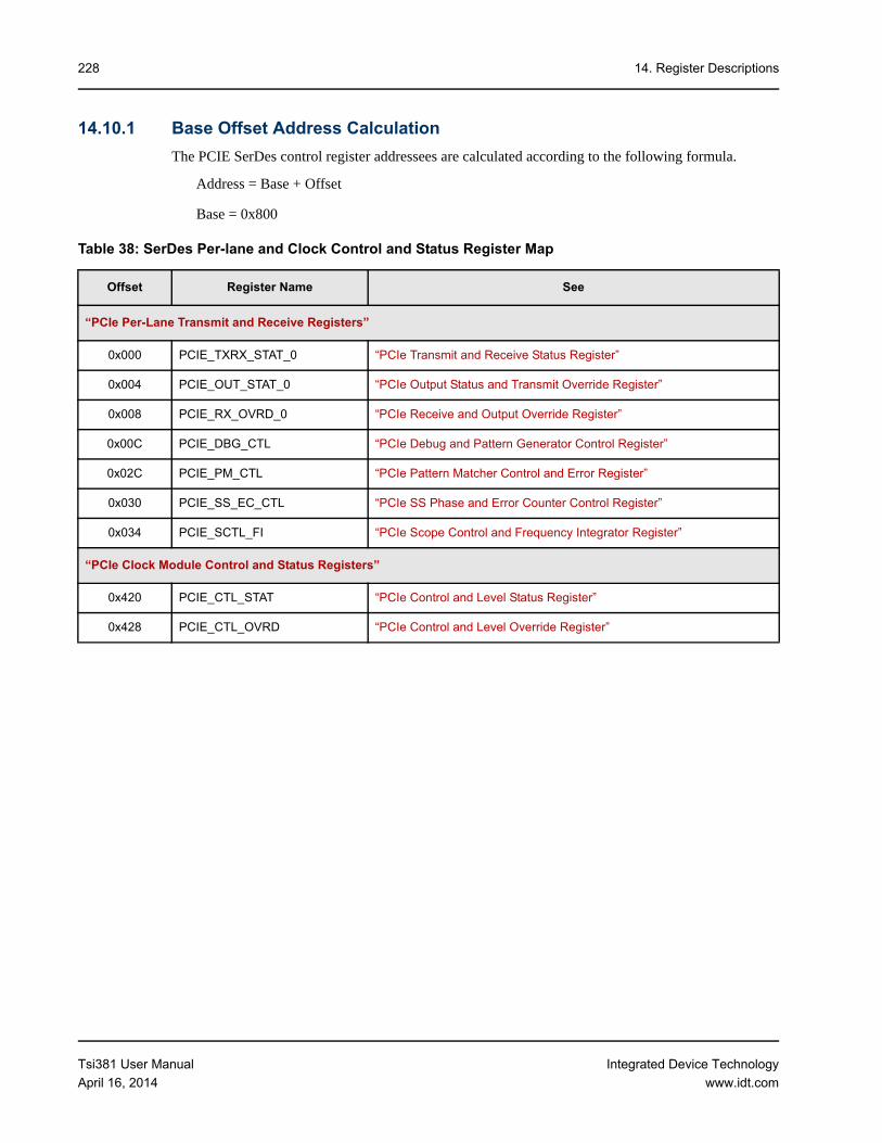
14. Register Descriptions228
14.10.1 Base Offset Address Calculation
The PCIE SerDes control register addressees are calculated according to the following formula.
Address = Base + Offset
Base = 0x800
Table 38: SerDes Per-lane and Clock Control and Status Register Map
Offset Register Name See
“PCIe Per-Lane Transmit and Receive Registers”
0x000 PCIE_TXRX_STAT_0 “PCIe Transmit and Receive Status Register”
0x004 PCIE_OUT_STAT_0 “PCIe Output Status and Transmit Override Register”
0x008 PCIE_RX_OVRD_0 “PCIe Receive and Output Override Register”
0x00C PCIE_DBG_CTL “PCIe Debug and Pattern Generator Control Register”
0x02C PCIE_PM_CTL “PCIe Pattern Matcher Control and Error Register”
0x030 PCIE_SS_EC_CTL “PCIe SS Phase and Error Counter Control Register”
0x034 PCIE_SCTL_FI “PCIe Scope Control and Frequency Integrator Register”
“PCIe Clock Module Control and Status Registers”
0x420 PCIE_CTL_STAT “PCIe Control and Level Status Register”
0x428 PCIE_CTL_OVRD “PCIe Control and Level Override Register”
Tsi381 User Manual
April 16, 2014
Integrated Device Technology
www.idt.com

14. Register Descriptions 229
14.10.2 PCIe Per-Lane Transmit and Receive Registers
14.10.3 PCIe Transmit and Receive Status Register
This register reflects the default state of the SerDes transmit and receive control inputs at power-up. Its reset value depends on various inputs. When its accompanying override registers are used, however (see “PCIe Output Status and Transmit Override Register” and “PCIe Receive and Output Override Register”), the relevant status bits are no longer valid.
Register name: PCIE_TXRX_STAT
Reset value: Undefined
Register offset: 0x000
Bits 7 6 5 4 3 2 1 0
3124 Reserved LOS_CTL Reserved
2316 RX_EQ_VAL Reserved RX_ALIGN_EN
Reserved HALF_RATE
15:08 Reserved TX_BOOST
07:00 TX_BOOST Reserved
Bits Name Description TypeResetValue
31:30 Reserved Reserved R 01
29:28 LOS_CTL LOS filtering mode control R Undefined
27:24 Reserved Reserved R Undefined
23:21 RX_EQ_VAL Receive Equalization control R 0b010
20 Reserved Reserved R 0
18:17 Reserved Reserved R Undefined
16 HALF_RATE Digital half-rate data control R Undefined
15:10 Reserved Reserved R 100000
9:6 TX_BOOST Transmit Boost control
Programmed boost value (ratio of drive level of transition bit to non-transition bit) is:
boost = -20*log(1-(tx_boost[3:0]+0.5)/32)dB, except that setting TX_BOOST to 0 produces 0dB of boost. This produces results up to 5.75dB in steps of ~0.37dB.
R 0b1011
5:0 Reserved Reserved R Undefined
Tsi381 User Manual
April 16, 2014
Integrated Device Technology
www.idt.com

14. Register Descriptions230
14.10.4 PCIe Output Status and Transmit Override Register
This register indicates the status of output signals. Its reset value depends on various inputs. The register also provides a method for overriding the value of TX_BOOST in the “PCIe Transmit and Receive Status Register”.
Register name: PCIE_OUT_STAT
Reset value: Undefined
Register offset: 0x004
Bits 7 6 5 4 3 2 1 0
3124 OVRD Reserved TX_BOOST
2316 TX_BOOST ReservedP
15:08 ReservedP
07:00 ReservedP LOS Reserved
Bits Name Description TypeResetValue
31 OVRD Enable override of relevant bits 16:30 in this register. R/W 0
30:26 Reserved Reserved R/W 00000
25:22 TX_BOOST Transmit Boost control
Programmed boost value (ratio of drive level of transition bit to non-transition bit) is:
boost = -20*log(1-(tx_boost[3:0]+0.5)/32)dB, except that setting TX_BOOST to 0 produces 0dB of boost. This produces results up to 5.75dB in steps of ~0.37dB.
R/W 0x0
21:3 ReservedP Preserve state on writes. R/W Undefined
2 LOS Loss of signal output R Undefined
1:0 Reserved Reserved R Undefined
Tsi381 User Manual
April 16, 2014
Integrated Device Technology
www.idt.com

14. Register Descriptions 231
14.10.5 PCIe Receive and Output Override Register
This register provides a method for overriding the values of LOS_CTL, RX_EQ_VAL, and RX_ALIGN_EN in the “PCIe Transmit and Receive Status Register”.
Register name: PCIE_RX_OVRD
Reset value: Undefined
Register offset: 0x008
Bits 7 6 5 4 3 2 1 0
3124 ReservedP
2316 ReservedP
15:08 ReservedP OVRD_2 LOS_CTL ReservedP
07:00 RX_EQ_VAL ReservedP RX_ALIGN_EN
ReservedP HALF_RATE
Bits Name Description TypeResetValue
31:15 ReservedP Preserve state on writes. R Undefined
14 OVRD_2 Enable override of relevant bits 0:13 in this register. R/W 0
13:12 LOS_CTL LOS filtering mode control
00 = Disabled
01-10 = Reserved
11 = Heavy filtering. The LOS signal is synchronous to the output of the prescaler. Heavy filtering means 128 +/- 5 cycles of no signal for LOS to be asserted.
R/W 01
11:8 ReservedP Preserve state on writes. R/W Undefined
7:5 RX_EQ_VAL Receive Equalization control
Internal linear equalizer boost is approximately = (rx_eq_val+1)*0.5dB
Example: 3’b100 = 2.5dB boost
R/W 000
4 ReservedP Preserve state on writes. R/W 1
3 RX_ALIGN_EN Enable Word Alignment
0 = Alignment (framer) disabled
1 = Alignment enabled
R/W 1
2:1 ReservedP Preserve state on writes. R/W 11
0 HALF_RATE Digital half-rate data control R/W 0
Tsi381 User Manual
April 16, 2014
Integrated Device Technology
www.idt.com

14. Register Descriptions232
14.10.6 PCIe Debug and Pattern Generator Control Register
This register controls the pattern generator in the SerDes.
Register name: PCIE_DBG_CTL
Reset value: 0x0000_0000
Register offset: 0x00C
Bits 7 6 5 4 3 2 1 0
3124 Reserved PATO
2316 PATO TRIGGER_ERR
MODE
15:08 Reserved
07:00 Reserved
Bits Name Description TypeResetValue
31:30 Reserved Reserved R 0
29:20 PATO Pattern for modes 3–5
Program the desired pattern in these 10 bits when using modes 3-5.
Note: This field returns to its reset value on reset.
R/W 0x00
19 TRIGGER_ERR Insert a single error into a LSB
Note: This field returns to its reset value on reset.
R/W 0
18:16 MODE Pattern to generate:
0 = Disabled
1 = lfsr15 (x15+x14+1)
2 = lfsr7 (x7+x6+1)
3 = Fixed word (PAT0)
4 = DC balanced word (PAT0, ~PAT0)
5 = Fixed pattern: (000, PAT0, 3ff, ~PAT0)
6–7 = Reserved
R/W 000
15:0 Reserved Reserved R 0
Tsi381 User Manual
April 16, 2014
Integrated Device Technology
www.idt.com

14. Register Descriptions 233
14.10.7 PCIe Pattern Matcher Control and Error Register
This register controls the pattern matcher in the SerDes.
Register name: PCIE_PM_CTL
Reset value: Undefined
Register offset: 0x02C
Bits 7 6 5 4 3 2 1 0
3124 OV14 COUNT
2316 COUNT
15:08 Reserved
07:00 Reserved SYNC MODE
Bits Name Description TypeResetValue
31 OV14 Overflow 14
0 = Inactive
1 = Multiply COUNT by 128
If OV14 is 1 and COUNT=2^15-1, signals overflow of counter.
Note: This bit may require two reads to get a stable value.a
a. Read operation on this register is pipelined. Two reads may be needed to get “current” value. The value is volatile; that is, the value may change at any time.The second read resets the counter.
R/W Undefined
30:16 COUNT Current error count
If OV14 field is active, then multiply count by 128.aR/W Undefined
15:4 Reserved Reserved R 0
3 SYNC Synchronize pattern matcher LFSR with incoming data must be turned on then off to enable checking.
Note: This bit returns to its reset value on reset
R/W 0
2:0 MODE Pattern to match:
0 = Disabled
1 = lfsr15
2 = lfsr7
3 = d[n] = d[n-10]
4 = d[n] = !d[n-10]
5-7 = Reserved
R/W 000
Tsi381 User Manual
April 16, 2014
Integrated Device Technology
www.idt.com

14. Register Descriptions234
14.10.8 PCIe SS Phase and Error Counter Control Register
This register holds the current MPLL phase selector value and information for the associated error counter in the SerDes.
Register name: PCIE_SS_EC_CTL
Reset value: Undefined
Register offset: 0x030
Bits 7 6 5 4 3 2 1 0
3124 Reserved SS_PVAL
2316 SS_PVAL DTHR
15:08 OV14 COUNT
07:00 COUNT
Bits Name Description TypeResetValue
31:28 Reserved Reserved R 0
27:17 SS_PVAL Phase value from zero referencea
a. Read operation on this register is pipelined. Two reads may be needed to get “current” value. The value is volatile; that is, the value may change at any time.The second read resets the counter.
R/W 0x000
16 DTHR Bits below the useful resolutiona R/W 0
15 OV14 0verflow 14
0 = Inactive
1 = Multiply COUNT by 128.
If OV14=1 and COUNT=2^15-1, signals overflow of counter.a
R/W Undefined
14:0 COUNT Current error count
If OV14 field is active, then multiply count by 128.aR/W Undefined
Tsi381 User Manual
April 16, 2014
Integrated Device Technology
www.idt.com

14. Register Descriptions 235
14.10.9 PCIe Scope Control and Frequency Integrator Register
Register name: PCIE_SCTL_FI
Reset value: 0000_0000
Register offset: 0x034
Bits 7 6 5 4 3 2 1 0
3124 Reserved
2316 Reserved
15:08 Reserved FVAL
07:00 FVAL DTHR_F
Bits Name Description TypeResetValue
31:14 Reserved Reserved R/W 0
13:1 FVAL Frequency is 1.526*VAL ppm from the reference. Value is a signed integer format (2’s complement).
Note: This field may require two “reads” to get a stable value.
R/W 0
0 DTHR_F Bits below the useful resolution.
Note: This bit may require two “reads” to get a stable value.
R/W 0
Tsi381 User Manual
April 16, 2014
Integrated Device Technology
www.idt.com

14. Register Descriptions236
14.10.10 PCIe Clock Module Control and Status Registers
14.10.11 PCIe Control and Level Status Register
This register indicates the status of various control inputs. Its reset value depends on inputs. When its accompanying override register is used, however (see “PCIe Control and Level Override Register”), the relevant status bits are no longer valid.
Register name: PCIE_CTL_STAT
Reset value: Undefined
Register offset: 0x420
Bits 7 6 5 4 3 2 1 0
3124 Reserved TX_LVL LOS_LVL
2316 LOS_LVL ACJT_LVL
15:08 Reserved
07:00 Reserved
Bits Name Description TypeResetValue
31 Reserved Reserved R 1
30:26 TX_LVL Fine Resolution setting of Tx signal level.
Equation: Pk-Pk output level (without attenuation) = 1230 x (48 + tx_lvl/2)/63.5 mV Vdiff-pp
Note: TX_LVL should be set to >= 0x1010 (which results in an output of 1Vp-p). For more information on available settings, see Table 39.
R 0x10
25:21 LOS_LVL Loss of Signal Detector level. R 0x12
20:16 ACJT_LVL AC JTAG Comparator level. R 0x00
15:0 Reserved Reserved R 1
Tsi381 User Manual
April 16, 2014
Integrated Device Technology
www.idt.com

14. Register Descriptions 237
14.10.12 PCIe Control and Level Override Register
The register provides a method for overriding the value of TX_LVL, LOS_LVL, and ACJT_LVL in the “PCIe Control and Level Status Register”.
Register name: PCIE_CTL_OVRD
Reset value: Undefined
Register offset: 0x428
Bits 7 6 5 4 3 2 1 0
3124 OVRD TX_LVL LOS_LVL
2316 LOS_LVL ACJT_LVL
15:08 Reserved
07:00 Reserved
Bits Name Description TypeResetValue
31 OVRD Override all level controls. R/W 0
30:26 TX_LVL Fine Resolution setting of Tx signal level.
Equation: Pk-Pk output level (without attenuation) = 1230 x (48 + tx_lvl/2)/63.5 mV Vdiff-pp
Note: TX_LVL should be set to >= 0x1010 (which results in an output of 1Vp-p). For more information on available settings, see Table 39.
R/W 0x10
25:21 LOS_LVL Loss of Signal Detector level R/W 0x10
20:16 ACJT_LVL AC JTAG Receiver Comparator level
This sets the hysteresis level for AC JTAG. For information on setting the correct voltage levels, see IEEE 1149.6.
R/W 0x10
15:0 ReservedP Preserve state on writes. R/W Undefined
Table 39: TX_LVL Values
TX_LVL Value TX_LVL[0:4] Vdiff-pp (mV)
0 0x00 5'b00000 929.8
1 0x01 5'b00001 939.4
2 0x02 5'b00010 949.1
3 0x03 5'b00011 958.8
4 0x04 5'b00100 968.5
5 0x05 5'b00101 978.2
Tsi381 User Manual
April 16, 2014
Integrated Device Technology
www.idt.com

14. Register Descriptions238
6 0x06 5'b00110 987.9
7 0x07 5'b00111 997.6
8 0x08 5'b01000 1007.2
9 0x09 5'b01001 1016.9
10 0xA 5'b01010 1026.6
11 0xB 5'b01011 1036.3
12 0xC 5'b01100 1046.0
13 0xD 5'b01101 1055.7
14 0xE 5'b01110 1065.4
15 0xF 5'b01111 1075.0
16 0x10 5'b10000 1084.7
17 0x11 5'b10001 1094.4
18 0x12 5'b10010 1104.1
19 0x13 5'b10011 1113.8
20 0x14 5'b10100 1123.5
21 0x15 5'b10101 1133.1
22 0x16 5'b10110 1142.8
23 0x17 5'b10111 1152.5
24 0x18 5'b11000 1162.2
25 0x19 5'b11001 1171.9
26 0x1A 5'b11010 1181.6
27 0x1B 5'b11011 1191.3
28 0x1C 5'b11100 1200.9
29 0x1D 5'b11101 1210.6
30 0x1E 5'b11110 1220.3
31 0x1F 5'b11111 1230.0
Table 39: TX_LVL Values (Continued)
TX_LVL Value TX_LVL[0:4] Vdiff-pp (mV)
Tsi381 User Manual
April 16, 2014
Integrated Device Technology
www.idt.com

239
15. Electrical Characteristics
Topics discussed include the following:
• “Absolute Maximum Ratings”
• “Recommended Operating Conditions”
• “Power Characteristics”
• “Power Supply Sequencing”
• “DC Operating Characteristics”
• “AC Timing Specifications”
• “AC Timing Waveforms”
15.1 Absolute Maximum Ratings
Table 40: Absolute Maximum Ratings – PCI
Symbol Parameter Minimum Maximum Units
TSTG Storage temperature -55 125 oC
TC Case temperature under bias -40 120 oC
Voltage with respect with ground
VDD 1.2V DC core logic supply voltage -0.5 2.0 V
VDD_PCIE 1.2V DC PCIe digital supply voltage -0.3 1.7 V
VDDA_PLL 1.2V DC PLL analog supply voltage -0.5 2.0 V
VDD_PCI 3.3V DC I/O supply voltage -0.5 4.1 V
VDDA_PCIE 3.3V DC PCIe analog supply voltage -0.5 4.6 V
VIO_PCI PCI Interface I/O voltage -0.5 6.6 V
VIL Minimum signal input voltage -0.5 - V
VIH Maximum signal input voltage - VDDa + 0.5
a. The VDD reference is dependent on the input pad supply rail.
V
Tsi381 User Manual
April 16, 2014
Integrated Device Technology
www.idt.com

15. Electrical Characteristics240
15.2 Recommended Operating Conditions
15.3 Power Characteristics
Table 42: Recommended Operating Conditions
Symbol Parameter Minimum Maximum Units Notes
VDD_PCI 3.3V DC I/O supply voltage 3.0 3.6 V -
VDDA_PCIE 3.3V DC PCIe supply voltage 3.0 3.6 V -
VDD 1.2V DC core supply voltage 1.14 1.26 V -
VDD_PCIE 1.2V DC PCIe digital supply voltage 1.14 1.26 V -
VDDA_PLL 1.2V DC PLL supply voltage 1.14 1.26 V -
VIO_PCI PCI Interface I/O voltage VDD_PCI 5.25 V -
Vripple1 Power Supply Ripple for Voltage Supplies: VDD and VDD_PCI
- 100 mVpp -
Vripple2 Power Supply Ripple for Voltage Supplies: VDD_PCIE, VDDA_PCIE, VDDA_PLL
- 50 mVpp -
TA Ambient temperature -40 85 oC a, b
a. No heat sink, no air flow.
b. Higher ambient temperatures are permissible provided TJUNC is not violated. For heat sink and air flow requirements for higher temperature operation, see “Thermal Characteristics”.
TJUNC Junction temperature -40 125 oC -
Table 43: Power Characteristics
PCI
Frequency Symbol Parameter
Power (mW) Avg. Current (mA)
Typ.a Max.b Typ.a Max.b
66 MHz VDD 1.2V core 186 194 155 163
VDD_PCI 3.3V PCI and CMOS I/O 492 700 149 202
VDDA_PLL and VDD_PCIE 1.2V analog for PLL and SerDes 35 38 29 30
VDDA_PCIE 3.3V analog power for SerDes 96 104 29 30
PTOTAL Total chip power 809 1036 - -
Tsi381 User Manual
April 16, 2014
Integrated Device Technology
www.idt.com

15. Electrical Characteristics 241
15.4 Power Supply SequencingThe Tsi381 does not have any power sequencing constraints.
15.5 DC Operating Characteristics
33 MHz VDD 1.2V core 170 172 142 143
VDD_PCI 3.3V PCI and CMOS I/O 422 581 128 176
VDDA_PLL and VDD_PCIE 1.2V analog for PLL and SerDes 35 35 29 29
VDDA_PCIE 3.3V analog power for SerDes 96 96 29 29
PTOTAL Total chip power 723 884 - -
a. Typical current is measured at nominal voltages with PCI I/O attached to four loads, with random bidirectional traffic.
b. Maximum current is measured at nominal voltages with all outputs switching simultaneously, driving four loads.
Table 44: DC Operating Characteristics
Symbol Parameter Condition Minimum Maximum Units Notes
VIL_PCI5V PCI Input Low Voltage for 5V Signals
- -0.5 0.8 V -
VIH_PCI5V PCI Input High Voltage for 5V Signals
- 2.0 VIO_PCI + 0.5 V -
VOL_PCI PCI Output Low Voltage IOL = 1500uA - 0.1VDD_PCI V -
VOH_PCI PCI Output High Voltage
IOH 0.9VDD_PCI - V -
VOL_PCI5V PCI Output Low Voltage for 5V Signals
IOL = 6mA - 0.55 V -
VOH_PCI5V PCI Output High Voltage for 5V Signals
IOH = -2mA 2.4 - V -
VOH_33 3.3 CMOS Output High Voltage
IOH = -6mA VDD_PCI - 0.5 - V -
VOL_33 3.3 CMOS Output Low Voltage
IOL = 6mA - 0.4 V -
Table 43: Power Characteristics (Continued)
PCI
Frequency Symbol Parameter
Power (mW) Avg. Current (mA)
Typ.a Max.b Typ.a Max.b
Tsi381 User Manual
April 16, 2014
Integrated Device Technology
www.idt.com

15. Electrical Characteristics242
15.6 AC Timing SpecificationsThis section discusses AC timing specifications for the Tsi381.
15.6.1 PCI Interface AC Signal Timing
VIH_33 3.3 CMOS Input High Voltage
- 2 VDD_PCI + 0.5 V -
VIL_33 3.3 CMOS Input Low Voltage
- -0.5 0.8 V -
CIN_PCI Input Pin Capacitance - - 8.8 pF -
CCLK_PCI Clock Pin Capacitance
PCI_CLK
- - 7.5 pF -
LIN_PCI Input Pin Inductance - - 8.3 nH -
LCLK_PCI Clock Pin Inductance
PCI_CLK
- - 4.9 nH -
Table 45: PCI Clock (PCI_CLK) Specification
Symbol Parameter Min Max Units Notes
TF_PCI PCI Clock Frequency 25 66 MHz a
a. The clock frequency may not change beyond the spread-spectrum limits except while device reset is asserted.
TC_PCI PCI Clock Cycle Time 15 40 ns a b
b. The minimum clock period must not be violated for any single clock cycle.
TCH_PCI PCI Clock High Time 6 - ns -
TCL_PCI PCI Clock Low Time 6 - ns -
TSR_PCI PCI Clock Slew Rate 1 6 V/ns c
c. This slew rate must be met across the minimum peak-to-peak portion of the clock waveform.
TSKEW PCI Output Clock Skew - 0.5 ns -
Spread Spectrum Requirements
fMOD_PCI PCI_CLK Clock modulation frequency 30 33 kHz -
fSPREAD_PCI PCI_CLK Clock frequency spread -1 0 % -
Table 44: DC Operating Characteristics (Continued)
Symbol Parameter Condition Minimum Maximum Units Notes
Tsi381 User Manual
April 16, 2014
Integrated Device Technology
www.idt.com

15. Electrical Characteristics 243
Table 46: AC Specifications for PCI Interface
Symbol Parameter
PCI 66 PCI 33
Units NotesMin Max Min Max
TOV1 Clock to Output Valid Delay for bused signals
2 6 2 11 ns a, b, c
TOV2 Clock to Output Valid Delay for point-to-point signals
2 6 2 12 ns a, b, c
TOF Clock to Output Float Delay - 14 - 28 ns a, d
TIS1 Input Setup to clock for bused signals 3 - 7 - ns c, e, f
TIS2 Input Setup to clock for point-to-point signals
5 - 10,12 - ns c, d
TIH1 Input Hold time from clock 0 - 0 - ns d
TRST Reset Active Time 1 - 1 - ms -
TRF Reset Active to output float delay - 40 - 40 ns g
TIS3 P[x]_REQ64_B to Reset setup time 10 - 10 - clocks -
TIH2 Reset to P[x]_REQ64_B hold time 0 50 0 50 ns -
a. See the timing measurement conditions in Figure 42.
b. See Figures 43, 44, and 45.
c. Setup time for point-to-point signals applies to P[x]_REQ_B and P[x]_GNT_B only. All other signals are bused.
d. For purposes of Active/Float timing measurements, the HI-Z or “Off” state is defined to be when the total current delivered through the component pin is less than or equal to the leakage current specification.
e. See the timing measurement conditions in Figure 41.
f. Setup time applies only when the device is not driving the pin. Devices cannot drive and receive signals at the same time.
g. All output drivers must be floated when PCIE_PERSTn is active.
Tsi381 User Manual
April 16, 2014
Integrated Device Technology
www.idt.com

15. Electrical Characteristics244
15.6.2 PCIe Differential Transmitter Output Specification
The following table lists the specification of parameters for the differential output of the PCIe lanes.
Table 47: PCIe Differential Transmitter Output Specification
Symbol Parameter Min. Nom. Max. Units Comments
UI Unit Interval 399.88 400 400.12 ps Each UI is 400ps +/-300ppm. UI does not account for SSC dictated variations. See Note 1.
VTX-DIFFp-p Differential Peak to Peak Output Voltage programmed to tx_lvl=5b’01001 and tx_boost = 0
0.800 - 1.2 V VTX-DIFFp-p = 2*|VTX-D+ - VTX-D-|
See Note 1.
VTX-DE-RATIO De-emphasized Differential Output Voltage (Ratio)
-3.0 -3.5 -4.0 dB This is the ratio of the VTX-DIFFp-p of the second and following bits after a transition divided by the VTX-DIFFp-p of the first bit after a transition.
See Note 2
TTX-EYE Minimum TX Eye Width
0.75 - - UI The maximum Transmitter jitter can be derived as TTX-MAX-JITTER = 1 - TTX-EYE = 0.25 UI.
This parameter is measured with the equivalent of a zero jitter reference clock. See Notes 2 and 3.
TTX-EYE-MEDIAN-
to-MAX-JITTER
Maximum time between the jitter median and maximum deviation from the median
- - 0.125 UI Jitter is defined as the measurement variation of the crossing points (VTX-DIFF = 0V) in relation to recovered TX UI.
To be measured after the clock recovery function in Section 4.3.3.2 of the PCI Express Base Specification Rev 1.1. See Notes 2 and 3.
TTX-RISE, TTX-FALL D+/D- TX Output Rise/Fall Time
0.125 - - UI See Notes 2 and 5.
VTX-CM-ACp RMS AC Peak Common Mode Output Voltage
- - 20 mV VTX-CM-ACp = RMS(|VTX-D+ + VTX-D-|/2 - VTX-CM-DC)
VTX-CM-DC = DC(AVG) of |VTX-D+ + VTX-D-|/2
See Note 2
VTX-CM-DC-ACTIVE-
IDLE-DELTA
Absolute Delta of DC Common Mode Voltage During L0 and Electrical Idle
0 - 100 mV |VTX-CM-DC [during L0] -VTX-CM-DC
[during electrical idle]| <= 100mV
VTX-CM-DC = DC(AVG) of |VTX-D+ + VTX-D-|/2 [L0]
VTX-CM-idle-DC = DC(AVG) of |VTX-D+ + VTX-D-|/2 [Electrical Idle]
See Note 2
Tsi381 User Manual
April 16, 2014
Integrated Device Technology
www.idt.com

15. Electrical Characteristics 245
VTX_CM-LINE
-DELTA
Absolute Delta of DC Common Mode Voltage between D+ and D-
0 - 25 mV |VTX-CM-DC-D+ -VTX-CM-DC-D+| <= 25mV
VTX-CM-DC-D+ = DC(AVG) of |VTX-D+|
VTX-CM-DC-D- = DC(AVG) of |VTX-D-|
See Note 2
VTX-IDLE-DIFFp Electrical Idle Differential Peak Output Voltage
0 - 20 mV VTX-IDLE-DIFFp = |VTX-IDLE-D+ - VTX-IDLE-D-| <= 20mV
See Note 2.
VTX-RCV-DETECT The amount of voltage change allowed during Receiver Detection
- - 600 mV The total amount of voltage change that a transmitter can apply to sense whether a low impedance Receiver is present. See Section 4.3.1.8 of the PCI Express Base Specification (Revision 1.1).
VTX-DC-CM The TX DC Common Mode Voltage
0 - 3.6 V The maximum DC Common Mode voltage under any conditions. See Section 4.3.1.8 of the PCI Express Base Specification (Revision 1.1).
ITX-SHORT TX Short Circuit Current Limit
- - 90 mA The total current the Transmitter can provide when shorted to its ground
TTX-IDLE-MIN Minimum time spent in Electrical Idle
50 - - UI Minimum time a Transmitter must be in Electrical Idle. Used by the Receiver to start looking for an Electrical Idle Exit after successfully receiving an Electrical Idle ordered set.
TTX-IDLE-SET-to
-IDLE
Maximum time to transition to a valid Electrical Idle after sending an Electrical Idle ordered set
- - 20 UI After sending an Electrical Idle ordered set, the Transmitter must meet all Electrical Idle specifications within this time. This is considered a de-bounce time for the transmitter to meet Electrical Idle after transitioning from L0.
TTX-IDLE-to-DIFF
-DATA
Maximum time to transition to valid TX specifications after leaving an Electrical Idle condition
- - 20 UI Maximum time to meet all TX specifications when transitioning from Electrical Idle to sending differential data. This is considered a de-bounce time for the TX to meet all TX specifications after leaving Electrical Idle.
RLTX-DIFF Differential Return Loss
10 - - dB Measured over 50 MHz to 1.25 GHz.
See Note 4.
RLTX-CM Common Mode Return Loss
6 - - dB Measured over 50 MHz to 1.25 GHz.
See Note 4.
ZTX-DIFF-DC DC Differential TX Impedance
80 - 120 Ohms TX DC Differential Mode low impedance. See Note 6.
Table 47: PCIe Differential Transmitter Output Specification (Continued)
Symbol Parameter Min. Nom. Max. Units Comments
Tsi381 User Manual
April 16, 2014
Integrated Device Technology
www.idt.com

15. Electrical Characteristics246
Note that all Figure and Section references are to the PCI Express Base Specification (Revision 1.1).
1. No test load is necessarily associated with this value.
2. Specified at the measurement point into a timing and voltage compliance test load as shown in Figure 4-25 and measured using the clock recovery function in Section 4.3.3.2. (also see the transmitter compliance eye diagram in Figure 4-24).
3. A TTX-EYE = 0.75 UI provides for a total sum of deterministic and random jitter of TTX-JITTER-MAX = 0.25 UI for the Transmitter using clock recovery function specified in Section 4.3.3.2. The TTX-EYE-MEDIAN-to-MAX-JITTER specification ensures a jitter distribution in which the median and the maximum deviation from the median is less than half the total TX jitter budget using the clock recovery function specified in section 4.3.3.2. It should be noted that the median is not the same as the mean. The jitter median describes the point in time where the number of jitter points on either side is approximately equal as opposed the averaged time value. This parameter is to be met at the target bit error rate. The TTX_EYE_MEDIAN-to-MAX-JITTER is to be met using the compliance pattern at a sample size of 1,000,000 UI.
4. The Transmitter input impedance shall result in a differential return loss greater than or equal to 10 dB with a differential test input signal no less than 200mV (peak value, 400 mV differential peak to peak) swing around ground applied to D+ and D- lines and a common mode return loss greater than or equal to 6 dB over a frequency range of 50 MHz to 1.25 GHz. This input impedance requirement applies to all valid input levels. the reference impedance for return loss measurements is 50 Ohms to ground for both D+ and D- line (that is, as measured by a vector Network Analyzer with 50 Ohm probes - see Figure 4-25). Note that the series capacitors CTX is optional for the return loss measurement.
5. Measured between 20-80% at the Transmitter package pins into a test load as shown in Figure 4-25 for both VTX-D+ and VTX-D-.
6. ZTX-DIFF-DC is the small signal resistance of the transmitter measured at a DC operating point that is equivalent to that established by connecting a 100-Ohm resistor from D+ and D- while the TX is driving a static logic one or logic zero. Equivalently, this parameter can be derived by measuring the RMS voltage of the TX while transmitting a test pattern into two different differential terminations that are near 100 Ohms. Small signal resistance is measured by forcing a small change in differential voltage and dividing this by the corresponding change in current.
LTX-SKEW Lane-to-Lane Output Skew
-2.8 - 500 + 2 UI ps Static skew between any two Transmitter Lanes within a single Link
CTX AC Coupling Capacitor 75 - 200 nF All Transmitters must be AC coupled. The AC coupling is required either within the media or within the transmitting component itself.
Tcrosslink Crosslink Random Timeout
0 - 1 ms This random timeout helps resolve conflicts in crosslink configuration by eventually resulting in only one Downstream and one Upstream Port. See Section 4.2.6.3 of the PCI Express Base Specification (Revision 1.1).
Table 47: PCIe Differential Transmitter Output Specification (Continued)
Symbol Parameter Min. Nom. Max. Units Comments
Tsi381 User Manual
April 16, 2014
Integrated Device Technology
www.idt.com

15. Electrical Characteristics 247
Figure 38: Transmitter Eye Voltage and Timing Diagram1
1. This diagram is an excerpt from PCI Express Base Specification (Revision 1.1), Revision 1.1, “Transmitter Compliance Eye Diagrams,” page 225.
Tsi381 User Manual
April 16, 2014
Integrated Device Technology
www.idt.com

15. Electrical Characteristics248
15.6.3 PCIe Differential Receiver Input Specifications
The following table lists the specification of parameters for the differential output of the PCIe lanes.
Table 48: PCIe Differential Receiver Input Specifications
Symbol Parameter Min. Nom. Max. Units Comments
UI Unit Interval 399.88 400 400.12 ps Each UI is 400ps +/-300ppm. Ui does not account for SSC dictated variations.
See Note 7.
VRX-DIFFp-p Differential Peak to Peak Input Voltage
0.175 - 1.200 V VRX-DIFFp-p = 2*|VRX-D+ - VRX-D-|
See Note 8.
TRX-EYE Minimum RX Eye Width
0.4 - - UI The maximum interconnect media and Transmitter jitter that can be tolerated by the Receiver can be derived as TRX-MAX-JITTER = 1 - TRX-EYE = 0.6 UI.
See Notes 8, 9, and 10.
TRX-EYE-MEDIAN-
to-MAX-JITTER
Maximum time between the jitter median and maximum deviation from the median
- - 0.3 UI Jitter is defined as the measurement variation of the crossing points (VRX-DIFF = 0V) in relation to recovered TX UI.
To be measured after the clock recovery function in Section 4.3.3.2 of the PCI Express Base Specification (Revision 1.1).
See Notes 8and 9.
VRX-CM-ACp RMS AC Peak Common Mode Input Voltage
- - 150 mV VRX-CM-AC = |VRX-D+ + VRX-D-|/2 - VRX-CM-DC
VRX-CM-DC = DC(AVG) of |VRX-D+ + VRX-D-|/2
See Note 8.
RLRX-DIFF Differential Return Loss
10 - - dB Measured over 50 MHz to 1.25 GHz.
See Note 11.
RLRX-CM Common Mode Return Loss
6 - - dB Measured over 50 MHz to 1.25 GHz.
See Note 11.
ZRX-DIFF-DC DC Differential Input Impedance
80 - 120 Ohms RX DC Differential Mode impedance. See Note 12.
ZRX-DC DC Input Impedance 40 50 60 Ohms Required RX D+ as well as D- DC impedance (50 Ohm +/- 20% tolerance).
See Notes 8 and 12.
ZRX-HIGH-IMP-DC Powered Down DC Input Impedance
200K - - Ohms Required RX D+ as well as D- DC impedance when the Receiver terminations do not have power.
See Note 13.
Tsi381 User Manual
April 16, 2014
Integrated Device Technology
www.idt.com

15. Electrical Characteristics 249
7. No test load is necessarily associated with this value.
8. Specified at the measurement point and measured using the clock recovery function specified in Section 4.3.3.2. The test load in Figure 4-25 should be used as the RX device when taking measurements (also refer to the Receiver compliance eye diagram shown in Figure 4-26). If the clocks to the RX and TX are not derived from the same reference clock, the TX UI recovered using the clock recovery function specified in Section 4.3.3.2 must be used as a reference for the eye diagram.
9. The TRX-EYE-MEDIAN-to-MAX-JITTER specification ensures a jitter distribution in which the median and the maximum deviation from the median is less than half of the total 0.64. It should be noted that the median is not the same as the mean. The jitter median describes the point in time where the number of jitter points on either side is approximately equal as opposed the averaged time value. The RX UI recovered using the clock recovery function specified in Section 4.3.3.2 must be used as the reference for the eye diagram. This parameter is measured with the equivalent of a zero jitter reference clock. The TRX-EYE measurement is to be met at the target bit error rate. The TRX-EYE-MEDIAN-to-MAX-JITTER specification is to be met using the compliance pattern at a sample size of 1,000,000 UI.
10. For more information on the RX-EYE measurement, see the PCI Express Jitter and BER white paper.
11. The receiver input impedance shall result in a differential return loss greater than or equal to 10 dB with a differential test input signal of no less than 200 mV (peak value, 400mV differential peak to peak) swing around ground applied to D+ and D- lines and a common mode return loss greater than or equal to 6 dB (no bias required) over a frequency range of 50 MHz to 1.25 GHz. This input impedance requirement applies to all valid input levels. The reference impedance for the return loss measurements is 50 Ohms to ground for both D+ and D- lines (that is, as measured by a Vector Network Analyzer with 50-Ohm probes - see Figure 4-25). Note that the series capacitors CTX is optional for the return loss measurement.
12. Impedance during all LTSSM states. When transitioning from a Fundamental Reset to Detect (the initial state of the LTSSM) there is a 5ms transition time before the Receiver termination values must be met on all un-configured lanes of a port.
13. The RX DC Common Mode Impedance that exists when no power is present or Fundamental Reset is asserted. This helps ensure that the Receiver Detect circuit does not falsely assume a Receiver is powered on when it is not. This term must be measured at 200mV above the RX ground.
VRX-IDLE-DET-DIFFp Electrical Idle Detect Threshold
65 - 175 mV VRX-IDLE-DET-DIFFp = 2*|VRX-D+ - VRX-D-|
Measured at the package pins of the Receiver.
TRX-IDLE-DET-DIFF-E
NTERTIME
Unexpected Electrical Idle Enter Detect Threshold Integration Time
- - 10 ms An unexpected Electrical Idle (VRX-DIFFp-p < VRX-IDLE-DET-DIFFp-p) must be longer than TRX-IDLE-DET-ENTERTIME to signal an unexpected idle condition.
LRX-SKEW Total Skew - - 20 ns Skew across all lanes on a link. This includes variation in the length of a SKP ordered set (for example, COM and one to five SKP Symbols) at the RX as well as any delay differences arising from the interconnect itself.
Table 48: PCIe Differential Receiver Input Specifications (Continued)
Symbol Parameter Min. Nom. Max. Units Comments
Tsi381 User Manual
April 16, 2014
Integrated Device Technology
www.idt.com

15. Electrical Characteristics250
Figure 39: Minimum Receiver Eye Timing and Voltage Compliance Specification1
1. This diagram is an excerpt from PCI Express Base Specification, Revision 1.1, “Differential Receiver (RX) Input Specifications,” page 230.
Tsi381 User Manual
April 16, 2014
Integrated Device Technology
www.idt.com

15. Electrical Characteristics 251
15.6.4 Reference Clock
The following table lists the Tsi381’s electrical characteristics for the differential SerDes reference clock input (PCIE_REFCLK_n/p).
Figure 40: Weighing Function for RMS Phase Jitter Calculation
Table 49: Reference Clock (PCIE_REFCLK_n/p) Electrical Characteristics
Symbol Parameter Min. Typ. Max. Unit Notes
VDIFF Differential Input Voltage 350 710 850 mV -
VCM Differential Input Common Mode Range [(PCIE_REFCLK_p +PCIE_REFCLK_n)/2]
175 - 2000 mV
-
Fin Input Clock Frequency - 100 - MHz -
FPCIE_REFCLK_P/N Reference Clock Frequency Tolerance
-300 - +300 ppm ppm with respect to 100 MHz, based on the PCIe Specification.
Fin_DC Reference Clock Duty Cycle
40 50 60 % -
JCLK-REF Total Phase Jitter (rms) - - 3 psrms See a.
a. Total Permissible Phase Jitter on the Reference Clock is 3 ps rms. This value is specified with assumption that the measurement is performed with a 20 GSamples/s scope with more than 1 million samples. The zero-crossing times of each rising edges are recorded and an average Reference Clock is calculated. This average period may be subtracted from each sequential, instantaneous period to find the difference between each reference clock rising edge and the ideal placement to produce the Phase Jitter Sequence. The PSD of the phase jitter is calculated and integrated after being weighted with the transfer function shown in Figure 40. The square root of the resulting integral is the rms Total Phase Jitter.
Zin Input Impedance - - - - PCIe_REFCLK_p/n is a high-impedance input.
Magnitude
0 dB
20 dB/Decade 40 dB/Decade
1.5 MHz 10 MHz Frequency
Tsi381 User Manual
April 16, 2014
Integrated Device Technology
www.idt.com

15. Electrical Characteristics252
15.6.5 Boundary Scan Test Signal Timing
The following table lists the test signal timings for the Tsi381.
15.6.6 Reset Timing
The following table lists the reset signal timings for the Tsi381.
Table 50: Boundary Scan Test Signal Timings
Symbol Parameter Min Max Units Notes
TBSF JT_TCK Frequency 0 10 MHz -
TBSCH JT_TCK High Time 50 - ns Measured at 1.5V, a
a. Not tested.
TBSCL JT_TCK Low Time 50 - ns Measured at 1.5V, a
TBSCR JT_TCK Rise Time - 25 ns 0.8V to 2.0V, a
TBSCF JT_TCK Fall Time - 25 ns 2.0V to 0.8V, a
TSIS1 Input Setup to JT_TCK 10 - ns b
b. See Figure 41.
TBSIH1 Input Hold from JT_TCK 10 - ns b
TBSOV1 JT_TDO Output Valid Delay from falling edge of JT_TCK.
- 15 ns c, d
c. Outputs precharged to VDD33.
d. See Figure 42.
TOF1 JT_TDO Output Float Delay from falling edge of JT_TCK
- 15 ns c, e
e. A float condition occurs when the output current becomes less than ILO. Float delay is not tested (see Figure 42).
Table 51: Reset Timing
Symbol Parameter Min Max Units Notes
TPOR Power supplies in recommended operating range to de-assertion of device reset
100 - ms The PCIe specification requires reset (PCIE_PERSTn) to remain asserted for 100 ms after power supplies are valid.
TACTIVE Reset active time 1 - ms -
Tsi381 User Manual
April 16, 2014
Integrated Device Technology
www.idt.com

15. Electrical Characteristics 253
15.7 AC Timing WaveformsThis section contains AC timing waveforms for the Tsi381.
Figure 41: Input Timing Measurement Waveforms
- PCI_CLK clock stable to de-assertion of device reset
100 - us -
- Power-up strapping hold from de-assertion of device reset
0 - ns -
THIZ Assertion of reset to outputs tri-state - 10 ns -
Table 51: Reset Timing (Continued)
Symbol Parameter Min Max Units Notes
CLK
INPUT Valid VtestVtest
Vtest
TIS
TIH
Vtl
Vth
Vth
Vtl
Vmax
Tsi381 User Manual
April 16, 2014
Integrated Device Technology
www.idt.com

15. Electrical Characteristics254
Figure 42: Output Timing Measurement Waveforms
Figure 43: PCI TOV (max) Rising Edge AC Test Load
Figure 44: PCI TOV (max) Falling Edge AC Test Load
VtestCLK
OUTPUTFLOAT
VtriseOUTPUTDELAY RISE
OUTPUTDELAY FALL
Vtfall
TOV
TOV
TOF
Vtl
Vth
Output
TestPoint
10pF25
Output
10pF
25
VCC33
TestPoint
Tsi381 User Manual
April 16, 2014
Integrated Device Technology
www.idt.com

15. Electrical Characteristics 255
Figure 45: PCI TOV (min) AC Test Load
Output
TestPoint
10pF
1K
1K
VCC33
Tsi381 User Manual
April 16, 2014
Integrated Device Technology
www.idt.com

15. Electrical Characteristics256
Tsi381 User Manual
April 16, 2014
Integrated Device Technology
www.idt.com

257
16. Packaging
Topics discussed include the following:
• “Mechanical Diagram”
• “Thermal Characteristics”
• “Moisture Sensitivity”
Tsi381 User Manual
April 16, 2014
Integrated Device Technology
www.idt.com

16. Packaging258
16.1 Mechanical Diagram
Figure 46: Mechanical Diagram 144 pin 13x13mm BGA
Tsi381 User Manual
April 16, 2014
Integrated Device Technology
www.idt.com

16. Packaging 259
16.2 Thermal CharacteristicsHeat generated by the packaged silicon must be removed from the package to ensure the silicon is maintained within its functional and maximum design temperature limits. If heat buildup becomes excessive, the silicon temperature may exceed the temperature limits. A consequence of this is that the silicon may fail to meet the performance specifications and the reliability objectives may be affected.
Failure mechanisms and failure rate of a device has an exponential dependence on the silicon operating temperatures. Therefore, the control of the package, and by extension the Junction temperature, is essential to ensure product reliability. The Tsi381 is specified safe for operation when the Junction temperature is within the recommended limits as shown in Table 53.
Table 52 shows the simulated thermal characteristic (JB and JC) of the Tsi381 package.
Table 52: Thermal Characteristics
Table 53 shows the simulated Junction to Ambient (JA) characteristics of the Tsi381. The thermal resistance JA characteristics of a package depends of multiple variables other than just the package. In a typical application, designers must take into account various system-level and environmental characteristics, such as:
• Package mounting (vertical/horizontal)
• System airflow conditions (laminar/turbulent)
• Heat sink design and thermal characteristics
• Heat sink attachment method
• PWB size, layer count, and conductor thickness
• Influence of the heat dissipating components assembled on the PWB (neighboring effects)
The results in Table 53 are based on a JEDEC Thermal Test Board configuration (JESD51-9), and does not factor in the system-level characteristics described above. As such, these values are for reference only.
Table 53: Junction to Ambient Characteristics
Interface Results
JB 16.3°C/W
Jc 9.7°C/W
Device
JA at Specified Airflow (No heat sink)
0 m/s 1 m/s 2 m/s
Tsi381 21.8°C/W 20.0°C/W 19.3°C/W
Tsi381 User Manual
April 16, 2014
Integrated Device Technology
www.idt.com

16. Packaging260
Example of Thermal Data Usage
Based on above JA data and specified conditions, the Junction temperature of the Tsi381 with a 0 m/s airflow can be determined using the following formula:
TJ = JA * P + TAMB
Where:
• TJ is the Junction temperature
• P is the Power consumption
• TAMB is the Ambient temperature
For the BGA package, assuming a Power consumption of 1W and Ambient temperature of 85°C, the resultant Junction temperature would be 107.1°C. For the LQFP package, assuming a Power consumption of 1.04W and Ambient temperature of 85°C, the resultant Junction temperature would be 114.1°C.
Assuming a Power consumption of 1.3W and Ambient temperature of 85°C, the resultant Junction temperature would be 113.3°C.
Assuming a Power consumption of 1.5W and Ambient temperature of 85°C, the resultant Junction temperature would be 116.4°C.
16.3 Moisture SensitivityThe moisture sensitivity level (MSL) for the Tsi381 is 3.
Tsi381 User Manual
April 16, 2014
Integrated Device Technology
www.idt.com

261
17. Ordering Information
Topics discussed include the following:
• “Part Numbers”
• “Part Numbering Information”
17.1 Part Numbers
17.2 Part Numbering InformationThe part numbering system is explained as follows.
• ( ) – Indicates optional characters.
• Tsi – IDT system interconnect product identifier.
• NNNN – Product number (may be three or four digits).
• SS(S) – Maximum operating frequency or data transfer rate of the fastest interface. For operating frequency numbers, M and G represent MHz and GHz. For transfer rate numbers, M and G represent Mbps and Gbps.
Table 54: Part Numbers
Part Number Frequency Temperature Package Pin Count
Tsi381-66ILV 66 MHz Industrial RoHS/Green 144
Tsi381-66IL 66 MHz Industrial Eutectic 144
Tsi NNN(N) - SS(S) E P G (Z#)
IDT
pro
duct
iden
tifi
er
Pro
duct
num
ber
Ope
rati
ng f
requ
ency
Ope
rati
ng e
nvir
onm
ent
Pac
kage
type
Pro
toty
pe v
ersi
on s
tatu
s
RoH
S/G
reen
com
plia
nce
Tsi381 User Manual
April 16, 2014
Integrated Device Technology
www.idt.com

17. Ordering Information262
• E – Operating environment in which the product is guaranteed. This code may be one of the following characters:
— C - Commercial temperature range (0 to +70°C)
— I - Industrial temperature range (-40 to +85°C)
— E - Extended temperature range (-55 to +125°C)
• P – The Package type of the product:
— B - Ceramic ball grid array (CBGA)
— E, L, J, and K - Plastic ball grid array (PBGA)
— G - Ceramic pin grid array (CPGA)
— M - Small outline integrated circuit (SOIC)
— Q - Plastic quad flatpack (QFP)
• G – IDT products fit into three RoHS-compliance categories:
— Y - RoHS Compliant (6of6) – These products contain none of the six restricted substances above the limits set in the EU Directive 2002/95/EC.
— Y - RoHS Compliant (Flip Chip) – These products contain only one of the six restricted substances: Lead (Pb). These flip-chip products are RoHS compliant through the Lead exemption for Flip Chip technology, Commission Decision 2005/747/EC, which allows Lead in solders to complete a viable electrical connection between semiconductor die and carrier within integrated circuit Flip Chip packages.
— V - RoHS Compliant/Green - These products follow the above definitions for RoHS Compliance and meet JIG (Joint Industry Guide) Level B requirements for Brominated Flame Retardants (other than PBBs and PBDEs).
• Z# – Prototype version status (optional). If a product is released as a prototype then a “Z” is added to the end of the part number. Further revisions to the prototype prior to production release would add a sequential numeric digit. For example, the first prototype version of device would have a “Z,” a second version would have “Z1,” and so on. The prototype version code is dropped once the product reaches production status.
Tsi381 User Manual
April 16, 2014
Integrated Device Technology
www.idt.com

263
A. PCIe Programmable Transmit and Receive Equalization
This appendix discusses the following topics:
• “Overview”
• “Transmit Drive Level and Equalization”
• “Receive Equalization”
A.1 OverviewThe Tsi381 has programmable drive strength and transmit boost (pre-emphasis), and receiver equalization. This functionality is described in the following sections.
A.2 Transmit Drive Level and EqualizationThe Tsi381’s programmable drive strength and transmit boost accommodates for electrical characteristics that can degrade the signal quality of a link connected to the Tsi381. Decreasing the drive strength of signals also provides the ability to reduce the power consumption of its PCIe port.
The drive strength of each lane can be controlled through TX_LVL in the “PCIe Control and Level Override Register”, and TX_BOOST in the “PCIe Output Status and Transmit Override Register” (see Figure 47).
The transmit boost functionality can be programmed by TX_BOOST in the “PCIe Output Status and Transmit Override Register”. The TX_BOOST field controls the drive level of subsequent non-transitional bits with respect to the transitional ones. The amount of boost is specified as a ratio of the boost drive strength to the TX_LVL drive strength, in steps of ~0.37dB.
The formula for calculating the TX_BOOST is shown in “PCIe Output Status and Transmit Override Register”.
The information in this appendix is for reference purposes only. Typical Tsi381-based designs do not require changes to the default settings for transmit drive level or receive equalization.
The Nominal Drive Level is 1.0 V +/-10%.
TheTX_LVL[4:0] field affects the Tx signal swing. For normal operation, set TX_LVL to a minimum of 1 V; for long reach compliance, set TX_LVL up to 1.26 V.
Tsi381 User Manual
April 16, 2014
Integrated Device Technology
www.idt.com

A. PCIe Programmable Transmit and Receive Equalization264
Figure 47: Drive Strength and Equalization Waveform
A.3 Receive EqualizationThe received signal can be internally boosted by configuring RX_EQ_VAL in the “PCIe Receive and Output Override Register”. The equation that uses the 3-bit field is listed below:
Receiver boost = (RX_EQ_VAL + 1)*0.5 dB
For example, setting RX_EQ_VAL[2:0] = 3’b100 results in a 2.5dB boost of the received signal. This boost is internal to the device and increases the eye opening when the signals arriving at the pins are degraded.
0.75 V (TX_LVL)
-2.32 dB (Programmed by TX_BOOST)
Tsi381 User Manual
April 16, 2014
Integrated Device Technology
www.idt.com

265
GlossaryAddress decode window The address range defined by a device’s base address registers when operating in non-transparent
addressing mode. If a transaction address on the bus falls within a device’s address decode window, the device claims the transaction.
Base and limit register A configuration register that stores memory or I/O address decode information in a device. If the address of a transaction falls within the window defined by a device’s base and limit registers, the device claims the transaction. Base and Limit registers are used only by transparent bridges.
CompactPCI cPCI. It is an adaptation of the PCI Local Bus Specification (Revision 2.2) for Industrial and/or embedded applications that require a more robust mechanical form factor than desktop PCI.
Completer (PCIe) The device that is targeted by a requester during a PCIe transaction. A requester reads data from a completer, or writes data to a completer. A requester can be either a root complex or an endpoint device.
Completer ID This value uniquely identifies the completer of a transaction request. It consists of a completer’s bus number, device number, and function number.
Configuration transaction A read or write access of a PCI device’s configuration registers.
Downstream port A PCIe port that points in the direction away from the root complex (for example, a root complex port).
Egress port A PCIe port that transmits a packet to another PCIe device.
Endpoint A type of PCIe device, or mode of operation, that function as requesters or completers of PCIe transactions (examples include Ethernet, USB, and graphic devices). If a PCIe port is not configured as a root complex or a switch then it is considered an endpoint. An endpoint can support up to eight functions.
Fairness algorithm Arbitration logic that helps low and high priority devices gain fair access to a peripheral bus. This logic also helps prevent deadlocks among bus-mastering devices in a system.
Flow control The method of communicating receive buffer status from a receiver to a transmitter to prevent receive buffer overflow and to allow transmitter compliance with ordering rules.
Hierarchy A PCIe fabric of all devices and links associated with a root complex. The devices can be connected either directly or indirectly (through switches and bridges) to the root complex.
Hot swap This refers to the process of inserting and extracting CompactPCI boards from an active system without adversely affecting system operation.
Ingress port A PCIe port that receives a packet from another PCIe device.
Link An interconnection between two PCIe devices. A link consists of either x1, x2, x4, x8, x16, or x32 pairs of signals between two devices. Each grouping of signals is referred to as a lane.
Memory-mapped I/O MIO. Memory-mapped I/O is used for non-prefetchable PCI memory transactions.
Tsi381 User Manual
April 16, 2014
Integrated Device Technology
www.idt.com

266
Message A TLP used to communicate information outside of the memory, I/O, and configuration spaces. Message TLPs are always posted, and may or may not contain data.
Non-transparent addressing
This type of addressing is used by a PCI bridging device to isolate the primary address map from the secondary address map. It provides address translation for PCI devices located in separate address domains with multiple host processors. This mode of operation, which is sometimes called embedded bridging, allows for distinct PCI memory spaces to be connected through defined windows with address translation from one memory domain to another.
PCI extended capabilities Optional features supported by the PCI Local Bus Specification. Some examples of extended capabilities include: Vital Product Data, Message Signaled Interrupts, and Slot Numbering. A device that supports extended capabilities uses a PCI capability list to access the features located in its PCI configuration space.
Prefetchable memory The process of prefetching memory occurs when a line of information from memory is read before a bus master requests it. If a bus master later requests the memory line, the bus target can supply it immediately. This type of memory access minimizes the time required to retrieve target memory.
Requester (PCIe) The device that originates a PCIe transaction. A requester can be either a root complex or an endpoint device.
Requester ID (PCIe) This value uniquely identifies the requester of a transaction. It consists of a requester’s bus number, device number, and function number.
Root complex This is a type of PCIe device, or mode of operation, that connects a host processor and memory sub-system to a PCIe fabric. The root complex generates transaction requests on behalf of the host processor — such as configuration, memory, and I/O — to other devices in the PCIe hierarchy. It also handles interrupts and power management events.
The root complex appears as P2P bridge(s) to the PCIe links, and can support one or more PCIe ports.
Transparent addressing This type of PCI addressing is used by a bridging device to support configuration mapping but not perform address translation between two buses. When a device is configured in transparent mode, it provides standard PCI bus bridging support through its base and limit registers. These registers define address decode windows for multiple bridges so that transactions can be passed transparently in a system. This enables devices that are connected to multiple bridging devices to share a single, unified address space.
Upstream port A PCIe port that points in the direction of the root complex (for example, an endpoint port).
Tsi381 User Manual
April 16, 2014
Integrated Device Technology
www.idt.com

267
Index
Aabsolute maximum ratings 239AC timing
PCI Interface 242AC timing specifications 242AC timing waveforms 253address decoding
I/O memory 48ISA 50memory-mapped I/O 45non-transparent 51opaque 55prefetchable memory 47VGA 50
advanced error reporting capability registers 206arbitration 73ASPM 108
Bbuffer
downstream non-posted 42downstream posted 42upstream non-posted 40upstream posted 41
buffer management 64bus arbiter 73
Cclocking
PCI 105PCIe 104
cold reset 102completer abort completion status errors 93configuration retry 61configuration transaction
overview 57Type 0 58Type 1 58Type 1 to special cycle 60Type 1 to Type 0 59Type 1 to Type 1 59
DD state transitions 112D0 state 111D3cold state 111D3hot state 111DC and operating characteristics 241device power states 111device register map 133document conventions
Integrated Device Technology
www.idt.com
document status 16numeric conventions 16symbols 16
downstreamdata path 38non-transparent registers 202
EECRC error 84EEPROM controller 115EEPROM device 116EEPROM image 118error handling 79
PCI 89PCIe 82
exclusive access 71
Fflow control
advertisements 63credits 43overview 42
GGPIO 78
Hhot reset 103
II/O addressing 48IEEE 1149.1 Interface 125interrupt handling 77interrupt routing 78interrupt sources 78ISA addressing 50
JJTAG 123
read access 126write access 125
JTAG test pins 127JTAG_TCK signal 34, 35JTAG_TDI signal 34JTAG_TDO signal 34JTAG_TMS signal 35JTAG_TRSTn signal 35
LL0 state 109L1 state 109L2/L3 ready 109L3 state 109LDn state 109
Tsi381 User Manual
April 16, 2014
Index268
LOs state 109
Mmaster-abort errors 87mechanical diagram 258memory-mapped I/O addressing 45message signaled interrupts (MSI) 77message signaled interrupts (MSI-X) 77message transactions 69message-based interrupts
enhanced message signaled interrupts 77message signaled interrupts 77
MSI generationGPIO 78interrupts 78
Nnon-transparent addressing 51non-transparent registers
downstream 202upstream 170
Oopaque addressing 55opaque registers 168operating frequency 261ordering information 261
Ppackage types 261part numbering information 261PCI capability registers 173PCI clocking 105PCI errors 90PCI Interface
AC timing 242PCI reset 103PCI transactions 67PCIe
receive equalization 264transmit drive level 263transmit equalization 263
PCIe capability registers 191PCIe clocking 104PCIe configuration space 130PCIe enhanced configuration 60PCIe link states 110PCIe reset 102PCIe transactions 68pin count 261poisoned TLP 83power characteristics 240power management 107power management event 112power states 108
Tsi381 User Manual
April 16, 2014
power supply sequencing 241prefetchable memory addressing 47prefetching algorithm 43
Rrecommended operating conditions 240register map 133requestor ID 64reset
PCI 103PCIe 102
round-robin arbitration 74
SSerDes TAP controller 127short term caching 44system errors 94
TTAP controller 124target-abort errors 88TCK signal 34, 35TDI signal 34TDO signal 34temperature 261TEST_BIDR_CTL signal (JTAG) 35thermal characteristics 259timeout errors 93timing waveforms 253TMS signal 35transaction forwarding
PCI to PCIe 65PCIe to PCI 64
transaction managementdownstream 40upstream 39
transaction ordering 70transactions supported
PCI 67PCIe 68
TRSTn signal 35Type 0 configuration transaction 58Type 1 configuration transaction 58Type 1 to special cycle configuration transaction 60Type 1 to Type 0 configuration transaction 59Type 1 to Type 1 configuration transaction 59typical applications 26
Uuncorrectable address/attribute errors 86uncorrectable data error 85Undefined 130unsupported request completion status errors 93upstream
data path 37
Integrated Device Technology
www.idt.com

Index 269
non-transparent registers 170
VVGA addressing 50
Wwarm reset 102
Integrated Device Technology
www.idt.com
Tsi381 User Manual
April 16, 2014

Index270
Tsi381 User Manual
April 16, 2014
Integrated Device Technology
www.idt.com

CORPORATE HEADQUARTERS6024 Silver Creek Valley RoadSan Jose, CA 95138
for SALES:800-345-7015 or 408-284-8200www.idt.com
for Tech Support:email: [email protected]
April 2014 Integrated Device Technology, Inc *Notice: The information in this document is subject to change without notice
DISCLAIMER Integrated Device Technology, Inc. (IDT) and its subsidiaries reserve the right to modify the products and/or specifications described herein at any time and at IDT’s sole discretion. All information in this document, including descriptions ofproduct features and performance, is subject to change without notice. Performance specifications and the operating parameters of the described products are determined in the independent state and are not guaranteed to perform the same way wheninstalled in customer products. The information contained herein is provided without representation or warranty of any kind, whether express or implied, including, but not limited to, the suitability of IDT’s products for any particular purpose, an impliedwarranty of merchantability, or non-infringement of the intellectual property rights of others. This document is presented only as a guide and does not convey any license under intellectual property rights of IDT or any third parties.
IDT’s products are not intended for use in life support systems or similar devices where the failure or malfunction of an IDT product can be reasonably expected to significantly affect the health or safety of users. Anyone using an IDT product in such amanner does so at their own risk, absent an express, written agreement by IDT.
Integrated Device Technology, IDT and the IDT logo are registered trademarks of IDT. Other trademarks and service marks used herein, including protected names, logos and designs, are the property of IDT or their respective third party owners.
Copyright 2009. All rights reserved.