ICODE SLIX2 2.5 kbit user memory size SL2S2602 · See Ref. 6 "General specification for 8" wafer on...
55
SL2S2602 ICODE SLIX2 Rev. 4.1 — 25 July 2017 Product data sheet 276341 COMPANY PUBLIC 1 General description The ICODE SLIX2 IC is the newest member of NXP’s SLIX product family. The chip is fully backwards compatible to SLIX and offers an increased user memory size, along with new outstanding features and performance: • NXP originality signature • Increased speed for Inventory management • Increased reading range • Increased robustness against detuning effects • 2.5 kbit user memory size • Flexible user memory segmentation with separate access conditions • Password protected on chip service cycle counter 1.1 Contactless energy and data transfer Whenever connected to a very simple and easy-to-produce type of antenna (as a result of the 13.56 MHz carrier frequency) made out of a few windings printed, winded, etched or punched coil, the ICODE SLIX2 IC can be operated without line of sight up to a distance of 1.5 m (gate width). No battery is needed. When the smart label is positioned in the field of an interrogator antenna, the high speed RF communication interface enables data to be transmitted up to 53 kbit/s. 1.2 Anticollision An intelligent anticollision function enables several tags to operate in the field simultaneously. The anticollision algorithm selects each tag individually and ensures that the execution of a transaction with a selected tag is performed correctly without data corruption resulting from other tags in the field. 1.3 Security and privacy aspects • Unique IDentifier (UID): The UID cannot be altered and guarantees the uniqueness of each label. • Originality signature: 32 byte ECC based originality signature. • Password protected memory management (Read/Write access): The user memory can be segmented into two pages and the access rights for read/ write access can be defined for each of them. This ensures that only authorized users get read/write access to the protected parts of the user memory (anti counterfeiting). READMULTIPLE BLOCK and (FAST) INVENTORY READ are compatible to ICODE SLI and ICODE SLIX. • Password protected Label Destroy:
Transcript of ICODE SLIX2 2.5 kbit user memory size SL2S2602 · See Ref. 6 "General specification for 8" wafer on...

SL2S2602ICODE SLIX2Rev. 4.1 — 25 July 2017 Product data sheet276341 COMPANY PUBLIC
1 General description
The ICODE SLIX2 IC is the newest member of NXP’s SLIX product family. The chip isfully backwards compatible to SLIX and offers an increased user memory size, along withnew outstanding features and performance:
• NXP originality signature• Increased speed for Inventory management• Increased reading range• Increased robustness against detuning effects• 2.5 kbit user memory size• Flexible user memory segmentation with separate access conditions• Password protected on chip service cycle counter
1.1 Contactless energy and data transferWhenever connected to a very simple and easy-to-produce type of antenna (as a resultof the 13.56 MHz carrier frequency) made out of a few windings printed, winded, etchedor punched coil, the ICODE SLIX2 IC can be operated without line of sight up to adistance of 1.5 m (gate width). No battery is needed. When the smart label is positionedin the field of an interrogator antenna, the high speed RF communication interfaceenables data to be transmitted up to 53 kbit/s.
1.2 AnticollisionAn intelligent anticollision function enables several tags to operate in the fieldsimultaneously. The anticollision algorithm selects each tag individually and ensuresthat the execution of a transaction with a selected tag is performed correctly without datacorruption resulting from other tags in the field.
1.3 Security and privacy aspects• Unique IDentifier (UID):
The UID cannot be altered and guarantees the uniqueness of each label.• Originality signature:
32 byte ECC based originality signature.• Password protected memory management (Read/Write access):
The user memory can be segmented into two pages and the access rights for read/write access can be defined for each of them. This ensures that only authorized usersget read/write access to the protected parts of the user memory (anti counterfeiting).READMULTIPLE BLOCK and (FAST) INVENTORY READ are compatible to ICODESLI and ICODE SLIX.
• Password protected Label Destroy:

NXP Semiconductors SL2S2602ICODE SLIX2
SL2S2602 All information provided in this document is subject to legal disclaimers. © NXP B.V. 2017. All rights reserved.
Product data sheet Rev. 4.1 — 25 July 2017COMPANY PUBLIC 276341 2 / 55
The 32-bit Destroy password enables an addressed label to be destroyed with theDESTROY SLIX2 command. That status is irreversible and the label will never respondto any command again.
• Password protected Privacy Mode:The 32-bit Privacy password enables a label to be set to the Privacy mode with theENABLE PRIVACY command. In this mode the label will not respond to any commandexcept the command GET RANDOM NUMBER, until it next receives the correctPrivacy password. This mode is especially designed to meet the increasing demand totake care of the customers privacy.
• Password protected EAS and AFI functionality:The 32-bit EAS/AFI password enables the addressed label to be set in a modewhere the EAS status, the EAS ID and/or the AFI value can only be changed if thecorrect EAS/AFI password needs to be transmitted before with the SET PASSWORDcommand.
• 16 bit counter:The last block of the user memory provides a special feature - the 16 bit counter.The counter can be increased by one with a WRITE command (optionally passwordprotected by the read password). The counter can be reset to an initial value with thewrite password.

NXP Semiconductors SL2S2602ICODE SLIX2
SL2S2602 All information provided in this document is subject to legal disclaimers. © NXP B.V. 2017. All rights reserved.
Product data sheet Rev. 4.1 — 25 July 2017COMPANY PUBLIC 276341 3 / 55
2 Features and benefits
2.1 ICODE SLIX2 RF interface (ISO/IEC 15693)• Contactless transmission of data and supply energy (no battery needed)• Operating distance: up to 1.5 m (depending on antenna geometry)• Operating frequency: 13.56 MHz (ISM, world-wide licence freely available)• Fast data transfer: up to 53 kbit/s• High data integrity: 16-bit CRC, framing• True anticollision• Electronic Article Surveillance (EAS)• Application Family Identifier (AFI) supported• Data Storage Format Identifier (DSFID)• ENABLE PRIVACY command with 32-bit Privacy password• DESTROY SLIX2 command with 32-bit Destroy password• Additional fast anticollision read• Persistent quiet mode to enable faster inventory speed• Write distance equal to read distance
2.2 EEPROM• 2560 bits user memory, organized in 80 blocks of 4 bytes each (last block reserved for
counter feature)• 50 years data retention• Write endurance of 100000 cycles
2.3 Security• Unique identifier for each device (8 byte)• 32 byte originality signature• Lock mechanism for each user memory block (write protection)• Lock mechanism for DSFID, AFI, EAS• Password (32-bit) protected memory management for Read access• Password (32-bit) protected memory management for Write access• Password (32-bit) protected Label Destroy• Password (32-bit) protected Privacy Mode• Password (32-bit) protected EAS and AFI functionality• 16 bit counter (optionally password protected with the read and write password)

NXP Semiconductors SL2S2602ICODE SLIX2
SL2S2602 All information provided in this document is subject to legal disclaimers. © NXP B.V. 2017. All rights reserved.
Product data sheet Rev. 4.1 — 25 July 2017COMPANY PUBLIC 276341 4 / 55
3 Applications
• Libraries• Item level tagging in pharmaceutical supply chains• Counterfeit protection for consumer goods• Industrial applications• Asset and document tracking

NXP Semiconductors SL2S2602ICODE SLIX2
SL2S2602 All information provided in this document is subject to legal disclaimers. © NXP B.V. 2017. All rights reserved.
Product data sheet Rev. 4.1 — 25 July 2017COMPANY PUBLIC 276341 5 / 55
4 Ordering informationTable 1. Ordering information
PackageType number
Name Description
Version
SL2S2602FUD/BG Wafer sawn, bumped wafer, 120 μm with 7 μ Polyimidespacer, on film frame carrier,Ci between LA and LB = 23.5 pF (typical)
-
SL2S2602FA8 MOA8 plastic lead less module carrier package;35 mm wide tape;Ci between LA and LB = 23.5 pF (typical)
SOT500-4

NXP Semiconductors SL2S2602ICODE SLIX2
SL2S2602 All information provided in this document is subject to legal disclaimers. © NXP B.V. 2017. All rights reserved.
Product data sheet Rev. 4.1 — 25 July 2017COMPANY PUBLIC 276341 6 / 55
5 Block diagram
001aam247
MOD
DEMOD
VREG
VDD
Clock
datain
dataout
R/W
ANALOGRF INTERFACE
PAD
PAD
LB
LA
RECT
Cres
DIGITAL CONTROL
ANTENNA
ANTICOLLISION
READ/WRITECONTROL
ACCESS CONTROL
EEPROM INTERFACECONTROL
RF INTERFACECONTROL
EEPROM
MEMORY
SEQUENCERCHARGE PUMP
CLK
Figure 1. Block diagram of ICODE SLIX2

NXP Semiconductors SL2S2602ICODE SLIX2
SL2S2602 All information provided in this document is subject to legal disclaimers. © NXP B.V. 2017. All rights reserved.
Product data sheet Rev. 4.1 — 25 July 2017COMPANY PUBLIC 276341 7 / 55
6 Pinning information
aaa-009401
LA LB
n.c.
Transparent top view
2 1
3
Figure 2. Pin configuration for SOT1122
Table 2. Pin description SOT1122Pin Symbol Description1 LB antenna RF input
2 LA antenna RF input
3 n.c. not connected
aaa-006273
LA LBtop view
Figure 3. Pin configuration for SOT500-4 (MOA8)
Table 3. Pin description SOT500-4 (MOA8)Pin Symbol DescriptionLA LA antenna RF input
LB LB antenna RF input

NXP Semiconductors SL2S2602ICODE SLIX2
SL2S2602 All information provided in this document is subject to legal disclaimers. © NXP B.V. 2017. All rights reserved.
Product data sheet Rev. 4.1 — 25 July 2017COMPANY PUBLIC 276341 8 / 55
7 Wafer Layout
aaa-016465
GND
LA LB
TEST
not to scale
Figure 4. Wafer SL2S2602FUD/BG layout and pin configuration for the bare die
7.1 Pin Description
Table 4. Bonding pad descriptionSymbol DescriptionLA antenna RF input
LB antenna RF input
GND ground
TEST test input
See Ref. 6 "General specification for 8" wafer on UV-tape with electronic fail diemarking".

NXP Semiconductors SL2S2602ICODE SLIX2
SL2S2602 All information provided in this document is subject to legal disclaimers. © NXP B.V. 2017. All rights reserved.
Product data sheet Rev. 4.1 — 25 July 2017COMPANY PUBLIC 276341 9 / 55
8 Mechanical specification
The ICODE SLIX2 wafers are available in 120 μm thickness. The 120 μm thick waferis enhanced with 7 μm Polyimide spacer providing better assembly tolerance (e.g.pressure).
8.1 Wafer specificationSee Ref. 6 "General specification for 8" wafer on UV-tape with electronic fail diemarking".
Table 5. Wafer specificationWafer
Designation each wafer is enscribed with batch number and wafer number
Diameter 200 mm (8 inches)
Thickness 120 μm ± 15 μm
Process CMOS 0.14 μm
Batch size 25 wafers
Dies per wafer 94823
Wafer backside
Material Si
Treatment ground and stress release
Ra minimum = 0.5 μmRoughness
Rt maximum = 5 μm
Chip dimensions
Die size without scribe 540 μm × 543 μm = 0.29322 mm2
Scribe line width
X-dimension 15 μm (scribe line width measured between nitride edges)
Y-dimension 15 μm (scribe line width measured between nitride edges)
Number of pads 4
Pad location non-diagonal/placed in chip corners
Distance pad to pad LA to LB 430 μm (center to center)
Distance pad to pad LB to TEST 371.5 μm (center to center)
Passivation on front
Type sandwich structure
Material PE-nitride (on top)
Thickness 1.75 μm total thickness of passivation
Polyimide spacer 7 μm ± 1 μm
Au bump
Material >99.9 % pure Au
Hardness 35 HV to 80 HV 0.005

NXP Semiconductors SL2S2602ICODE SLIX2
SL2S2602 All information provided in this document is subject to legal disclaimers. © NXP B.V. 2017. All rights reserved.
Product data sheet Rev. 4.1 — 25 July 2017COMPANY PUBLIC 276341 10 / 55
Shear strength >70 MPa
Height 25 μm[1]
Height uniformity
within a die ±2 μm
within a wafer ±3 μm
wafer to wafer ±4 μm
Bump flatness ±1.5 μm
Bump size
LA, LB 80 μm × 80 μm
TEST, GND 60 μm × 60 μm
variation ±5 μm
Under bump metallization sputtered TiW
1. Because of the 7 µm spacer, the bump will measure 18 µm relative height protrudingthe spacer.
8.1.1 Fail die identificationNo inkdots are applied to the wafer.
Electronic wafer mapping (SECS II format) covers the electrical test results andadditionally the results of mechanical/visual inspection.
See Ref. 6 "General specification for 8" wafer on UV-tape with electronic fail diemarking".
8.1.2 Map file distributionSee Ref. 6 "General specification for 8" wafer on UV-tape with electronic fail diemarking".

NXP Semiconductors SL2S2602ICODE SLIX2
SL2S2602 All information provided in this document is subject to legal disclaimers. © NXP B.V. 2017. All rights reserved.
Product data sheet Rev. 4.1 — 25 July 2017COMPANY PUBLIC 276341 11 / 55
9 Functional description
9.1 Block descriptionThe ICODE SLIX2 IC consists of three major blocks:
• Analog RF interface• Digital controller• EEPROM
The analog section provides stable supply voltage and demodulates data receivedfrom the reader for processing by the digital section. The analog section’s modulationtransistor also transmits data back to the reader.
The digital section includes the state machines, processes the protocol and handlescommunication with the EEPROM.
The label requires no internal power supply. Its contactless interface generates thepower supply and the system clock via the resonant circuitry by inductive coupling tothe interrogator. The interface also demodulates data that are transmitted from theinterrogator to the ICODE Label, and modulates the electromagnetic field for datatransmission from the ICODE Label to the interrogator.
Data are stored in a non-volatile memory (EEPROM).
9.2 Memory organizationThe 2560 bit user accessible EEPROM memory is divided into 80 blocks. A block is thesmallest access unit. Each block consists of 4 bytes (1 block = 32 bits). Bit 0 in eachbyte represents the least significant bit (LSB) and bit 7 the most significant bit (MSB),respectively.
The entire memory is divided into 3 parts:
• Configuration area– Within this part of the memory all required information is stored, such as UID, write
protection, access control information, passwords, AFI and EAS and originalitysignature. This memory area cannot be directly accessed.
• User memory– Within the 2528 bit memory (79 blocks) area the user data are stored. Direct read/
write access to this part of the memory is possible depending on the related securityand write protection conditions.
• 16 bit counter– The last block of the EEPROM memory (block 79) contains the 16 bit counter and the
counter password protection flag.

NXP Semiconductors SL2S2602ICODE SLIX2
SL2S2602 All information provided in this document is subject to legal disclaimers. © NXP B.V. 2017. All rights reserved.
Product data sheet Rev. 4.1 — 25 July 2017COMPANY PUBLIC 276341 12 / 55
Table 6. Memory organizationBlock Byte 0 Byte 1 Byte 2 Byte 3 Description
- Configuration area forinternal use
0
1
2
3
: : : : :
76
77
78
User memory:79 blocks,4 bytes each,316 bytes in total.
79 C0 C1 0x00 PROT Counter
Only Blocks 0 to 79 can be addressed with read and write commands.
Remark: Block 79 contains the 16 bit counter and can not be used to store user data.READ and WRITE commands to that block require special data considerations (refer tosection "16 bit counter feature").
9.2.1 Unique identifierThe 64-bit unique identifier (UID) is programmed during the production process accordingto ISO/IEC 15693-3 and cannot be changed afterwards.
The 64 bits are numbered according to ISO/IEC 15693-3 starting with LSB 1 and endingwith MSB 64. This is in contrast to the general used bit numbering within a byte.
The TAG type is a part of the UID (bit 41 to 48, next to the manufacturer code which is"04h" for NXP Semiconductors).
The TAG type of the ICODE SLIX2 IC is "01h".
Bit 37and bit 36 are used to differentiate between ICODE SLI, ICODE SLIX and ICODESLIX2 (refer to Table 8).
Table 7. Unique identifierMSB LSB64:57 56:49 48:41 40:1
"E0" "04" "01" IC manufacturer serial number
UID 7 UID 6 UID 5 UID 4 UID 3 UID 2 UID 1 UID 0
Table 8. Type indicator bitsBit 37 Bit 36 ICODE Type0 0 ICODE SLI
1 0 ICODE SLIX

NXP Semiconductors SL2S2602ICODE SLIX2
SL2S2602 All information provided in this document is subject to legal disclaimers. © NXP B.V. 2017. All rights reserved.
Product data sheet Rev. 4.1 — 25 July 2017COMPANY PUBLIC 276341 13 / 55
Bit 37 Bit 36 ICODE Type0 1 ICODE SLIX2
1 1 RFU
9.2.2 Originality signatureICODE SLIX2 features a cryptographically supported originality check. With this feature,it is possible to verify with a high confidence that the tag is using an IC manufactured byNXP Semiconductors. This check can be performed on personalized tags as well.
ICODE SLIX2 digital signature is based on standard Elliptic Curve Cryptography (curvename secp128r1), according to the ECDSA algorithm. The use of a standard algorithmand curve ensures easy software integration of the originality check procedure in NFCdevices without specific hardware requirements.
Each ICODE SLIX2 UID is signed with a NXP private key and the resulting 32-bytesignature is stored in a hidden part of the ICODE SLIX2 memory during IC production.
This signature can be retrieved using the READ_SIGNATURE command (refer toSection 9.5.3.20 "READ SIGNATURE") and can be verified in the NFC device by usingthe corresponding ECC public key provided by NXP. In case the NXP public key is storedin the reader device, the complete signature verification procedure can be performedoffline.
To verify the signature (for example with the use of the public domain crypto libraryOpenSSL) the tool domain parameters shall be set to secp128r1, defined within thestandards for elliptic curve cryptography SEC (Ref. 7).
9.2.3 Configuration of delivered ICsICODE SLIX2 ICs are delivered with the following configuration by NXP Semiconductors:
• Unique identifier is unique and read only• Write access conditions allow change to user blocks, AFI, DSFID, EAS and passwords
(password protection disabled)• All password bytes are 00h for the read and write protection password and the EAS/AFI
password• All password bytes are 0Fh for the Privacy and Destroy passwords• User data memory is not password protected• Password protected Privacy Mode is disabled• EAS and AFI password protection is disabled• Status of EAS mode is not defined• AFI is supported and not defined• DSFID is supported and not defined• User data memory is not defined
Remark: Because the EAS mode is undefined at delivery, the EAS mode shall be set(enabled or disabled) according to your application requirements during the test orinitialization phase.
Remark: If password protection is not required, depending on the targeted application, itis recommended to write random passwords during the label initialization.

NXP Semiconductors SL2S2602ICODE SLIX2
SL2S2602 All information provided in this document is subject to legal disclaimers. © NXP B.V. 2017. All rights reserved.
Product data sheet Rev. 4.1 — 25 July 2017COMPANY PUBLIC 276341 14 / 55
9.3 Communication principleFor detailed description of the protocol and timing please refer to ISO/IEC 15693-2(modulation, bit-coding, framing, Ref. 2) and ISO/IEC 15693-3 (anticollision, timing,protocol, Ref. 3).
For additional recommendations when using 100% ASK refer to Ref. 8.
9.4 State diagramThe state diagram illustrates the different states of the ICODE SLIX2.
aaa-016466
Any other command where theAddressed_flag is set
AND where inventory_flag is not set
Any other command Any other command wherethe Addressed_flag is set AND where inventory_flag is not set
or where inventory_flag AND AFI_flag is setor Inventory Read (extended mode) with both Goto Quiet flags set
or EAS Alarm
Quiet
Ready
Power-off
Selected
Select (UID)
Stay Quiet (UID)
Select (UID)
Select (UID)
In Field, if persistentquiet off
Any other commandwhere Selected_Flagis not set
In Field, if persistentquiet on
Reset to Ready
Reset to Ready whereSelected_Flag is set or
Select (different UID)
Stay Quiet (UID) orInventory Read (extended
mode) with Quiet_Flag is set
Stay Quiet Persistent (UID) orInventory Read (extended mode)with Persistent_Quiet_Flag is set
Out of Field
Reset to Ready Out of FieldOut of Field
Stay QuietPersistent
(UID)
Persistent Quiet
Figure 5. State diagram ICODE SLIX2
Remark: It is possible to set the ICODE SLIX2 IC into the Quiet and PersistentQiet.mode at the same time. In this case the behavior is the same as for the Quiet state

NXP Semiconductors SL2S2602ICODE SLIX2
SL2S2602 All information provided in this document is subject to legal disclaimers. © NXP B.V. 2017. All rights reserved.
Product data sheet Rev. 4.1 — 25 July 2017COMPANY PUBLIC 276341 15 / 55
only until the IC enters the Power-off state. The IC enters to the Persistent Quiet mode atthe next power-on if the persistent time has not been exceeded.
9.5 Supported commands
9.5.1 Mandatory commands
9.5.1.1 INVENTORY
As defined in ISO/IEC 15693-3.
Exception: If the Privacy or Destroy mode is enabled the label will not respond.
9.5.1.2 STAY QUIET
As defined in ISO/IEC 15693-3.
9.5.2 Optional commands
9.5.2.1 READ SINGLE BLOCK
As defined in ISO/IEC 15693-3.
Option 0 (Option flag not set) is supported.
Option 1 (Option flag set) is supported.
If the related page of the addressed block is protected with the Read-Password and thepassword has not been transmitted first with the SET PASSWORD command the labelwill respond according to the error handling (see Section 9.6 "Error handling").
Remark: Block 79 of the user memory contains the 16 bit counter feature and needs tobe treated differently (refer to section "16 bit counter feature").
9.5.2.2 WRITE SINGLE BLOCK
As defined in ISO/IEC 15693-3.
Option 0 (Option flag not set) is supported.
Option 1 (Option flag set) is supported.
If the addressed block is part of a write protected page or only protected with the ReadPassword (see Section 9.5.3.6 "PROTECT PAGE") and the password has not beentransmitted first with the SET PASSWORD command the label will respond according tothe error handling (see Section 9.6 "Error handling").
Remark: Block 79 of the user memory contains the 16 bit counter feature and needs tobe treated differently (refer to section "16 bit counter feature").
9.5.2.3 LOCK BLOCK
As defined in ISO/IEC 15693-3.
Option 0 (Option flag not set) is supported.

NXP Semiconductors SL2S2602ICODE SLIX2
SL2S2602 All information provided in this document is subject to legal disclaimers. © NXP B.V. 2017. All rights reserved.
Product data sheet Rev. 4.1 — 25 July 2017COMPANY PUBLIC 276341 16 / 55
Option 1 (Option flag set) is supported.
If the addressed block is part of a write protected page or only protected with the readpassword (see Section 9.5.3.6 "PROTECT PAGE") and the password has not beentransmitted first with the SET PASSWORD command, the label will respond according tothe error handling (see Section 9.6 "Error handling").
Remark: Block 79 of the user memory contains the 16 bit counter feature and can not belocked (refer to section "16 bit counter feature").
9.5.2.4 READ MULTIPLE BLOCKS
As defined in ISO/IEC 15693-3.
Option 0 (Option flag not set) is supported.
Option 1 (Option flag set) is supported.
If one of the addressed blocks is part of a page protected with the Read-Password andthe password has not been transmitted first with the SET PASSWORD command thelabel will respond according to the error handling (see Section 9.6 "Error handling").
Remark: Block 79 of the user memory contains the 16 bit counter feature and needs tobe treated differently (refer to section "16 bit counter feature").
9.5.2.5 SELECT
As defined in ISO/IEC 15693-3.
9.5.2.6 RESET TO READY
As defined in ISO/IEC 15693-3.
Remark: RESET TO READY also resets the label IC from the persistent quiet state(refer to Section 9.5.3.10 "INVENTORY READ" and Section 9.5.3.19 "STAY QUIETPERSISTENT")into the READY state.
9.5.2.7 WRITE AFI
As defined in ISO/IEC 15693-3.
Option 0 (Option flag not set) is supported.
Option 1 (Option flag set) is supported.
Remark: This command maybe password protected, refer to Section 9.5.3.16"PASSWORD PROTECT EAS/AFI".
9.5.2.8 LOCK AFI
As defined in ISO/IEC 15693-3.
Option 0 (Option flag not set) is supported.
Option 1 (Option flag set) is supported.
Remark: This command maybe password protected, refer to Section 9.5.3.16"PASSWORD PROTECT EAS/AFI".

NXP Semiconductors SL2S2602ICODE SLIX2
SL2S2602 All information provided in this document is subject to legal disclaimers. © NXP B.V. 2017. All rights reserved.
Product data sheet Rev. 4.1 — 25 July 2017COMPANY PUBLIC 276341 17 / 55
9.5.2.9 WRITE DSFID
As defined in ISO/IEC 15693-3.
Option 0 (Option flag not set) is supported.
Option 1 (Option flag set) is supported.
9.5.2.10 LOCK DSFID
As defined in ISO/IEC 15693-3.
Option 0 (Option flag not set) is supported.
Option 1 (Option flag set) is supported.
9.5.2.11 GET SYSTEM INFORMATION
As defined in ISO/IEC 15693-3.
The TAG type of the ICODE SLIX2 IC is "01h".
9.5.2.12 GET MULTIPLE BLOCK SECURITY STATUS
As defined in ISO/IEC 15693-3.
9.5.3 Custom commandsThe manufacturer code of NXP Semiconductors is defined in ISO/IEC 7816-6A1 (Ref. 5).It has the value "04h".
For the structure of custom commands please refer to ISO/IEC 15693-3.
If not explicitly specified differently all address modes are supported.
9.5.3.1 GET RANDOM NUMBER
Command code = B2h
The GET RANDOM NUMBER command is required to receive a random number fromthe label IC. The passwords that will be transmitted with the SET PASSWORD,ENABLEPRIVACY and DESTROY commands have to be calculated with the password and therandom number (see Section 9.5.3.2 "SET PASSWORD").
The different passwords are addressed with the password identifier.
Table 9. GET RANDOM NUMBER request formatSOF Flags GET
RANDOMNUMBER
IC Mfgcode
UID CRC16 EOF
- 8 bits 8 bits 8 bits 64 bitsoptional
16 bits -

NXP Semiconductors SL2S2602ICODE SLIX2
SL2S2602 All information provided in this document is subject to legal disclaimers. © NXP B.V. 2017. All rights reserved.
Product data sheet Rev. 4.1 — 25 July 2017COMPANY PUBLIC 276341 18 / 55
Table 10. GET RANDOM NUMBER response when Error_flag setSOF Flags Error code CRC16 EOF- 8 bits 8 bits 16 bits -
Table 11. GET RANDOM NUMBER response format when Error_flag NOT setSOF Flags Random
numberCRC16 EOF
- 8 bits 16 bits 16 bits -
9.5.3.2 SET PASSWORD
Command code = B3h
The SET PASSWORD command enables the different passwords to be transmitted tothe label to access the different protected functionalities of the following commands. TheSET PASSWORD command has to be executed just once for the related passwords ifthe label is powered.
Remark: The SET PASSWORD command can only be executed in Addressed orSelected mode except for the Privacy password. If the Privacy password is transmitted(see Section 9.5.3.9 "ENABLE PRIVACY"), the timing of the SET PASSWORD commandis write alike.
The XOR password has to be calculated with the password and two times the receivedrandom number from the last GET RANDOM NUMBER command:
XOR_Password[31:0] = Password[31:0] XOR {Random_Number[15:0],Random_Number[15:0]}.
The different passwords are addressed with the password identifier.
Table 12. SET PASSWORD request formatSOF Flags SET
PASSWORDIC Mfgcode
UID Passwordidentifier
XORpassword
CRC16 EOF
- 8 bits 8 bits 8 bits 64 bitsoptional
8 bits 32 bits 16 bits -
Table 13. Password IdentifierPassword identifier Password01h Read
02h Write
04h Privacy
08h Destroy
10h EAS/AFI

NXP Semiconductors SL2S2602ICODE SLIX2
SL2S2602 All information provided in this document is subject to legal disclaimers. © NXP B.V. 2017. All rights reserved.
Product data sheet Rev. 4.1 — 25 July 2017COMPANY PUBLIC 276341 19 / 55
Table 14. SET PASSWORD response format when Error_flag setSOF Flags Error code CRC16 EOF- 8 bits 8 bits 16 bits -
Table 15. SET PASSWORD response format when Error_flag NOT setSOF Flags CRC16 EOF- 8 bits 16 bits -
Remark: If the IC receives an invalid password, it will not execute any followingcommand until a Power-On Reset (POR) (RF reset) is executed.
9.5.3.3 WRITE PASSWORD
Command code = B4h
The WRITE PASSWORD command enables a new password to be written into therelated memory if the related old password has already been transmitted with a SETPASSWORD command and the addressed password is not locked (see Section 9.5.3.4"LOCK PASSWORD").
Remark: The WRITE PASSWORD command can only be executed in addressedor selected mode. The new password takes effect immediately which means that thenew password has to be transmitted with the SET PASSWORD command to accessprotected blocks/pages.
The different passwords are addressed with the password identifier.
The timing of the command is write alike.
Option 0 (Option flag not set) is supported.
Option 1 (Option flag set) is supported.
Table 16. WRITE PASSWORD request formatSOF Flags WRITE
PASSWORDIC Mfgcode
UID Passwordidentifier
Password CRC16 EOF
- 8 bits 8 bits 8 bits 64 bitsoptional
8 bits 32 bits 16 bits -
Table 17. Password IdentifierPassword identifier Password01h Read
02h Write
04h Privacy
08h Destroy
10h EAS/AFI

NXP Semiconductors SL2S2602ICODE SLIX2
SL2S2602 All information provided in this document is subject to legal disclaimers. © NXP B.V. 2017. All rights reserved.
Product data sheet Rev. 4.1 — 25 July 2017COMPANY PUBLIC 276341 20 / 55
Table 18. WRITE PASSWORD response format when Error_flag setSOF Flags Error code CRC16 EOF- 8 bits 8 bits 16 bits -
Table 19. WRITE PASSWORD response format when Error_flag NOT setSOF Flags CRC16 EOF- 8 bits 16 bits -
9.5.3.4 LOCK PASSWORD
Command code = B5h
The LOCK PASSWORD command enables the addressed password to be locked if therelated password has already been transmitted with a SET PASSWORD command. Alocked password cannot be changed.
The different passwords are addressed with the password identifier.
The timing of the command is write alike.
Option 0 (Option flag not set) is supported.
Option 1 (Option flag set) is supported.
Table 20. LOCK PASSWORD request formatSOF Flags LOCK
PASSWORDIC Mfgcode
UID Passwordidentifier
CRC16 EOF
- 8 bits 8 bits 8 bits 64 bitsoptional
8 bits 16 bits -
Table 21. Password identifierPassword identifier Password01h Read
02h Write
04h Privacy
08h Destroy
10h EAS/AFI
Table 22. LOCK PASSWORD response format when Error_flag setSOF Flags Error code CRC16 EOF- 8 bits 8 bits 16 bits -

NXP Semiconductors SL2S2602ICODE SLIX2
SL2S2602 All information provided in this document is subject to legal disclaimers. © NXP B.V. 2017. All rights reserved.
Product data sheet Rev. 4.1 — 25 July 2017COMPANY PUBLIC 276341 21 / 55
Table 23. LOCK PASSWORD response format when Error_flag NOT setSOF Flags CRC16 EOF- 8 bits 16 bits -
9.5.3.5 64 BIT PASSWORD PROTECTION
Command code = BBh
The 64-bit PASSWORD PROTECTION command enables the Label IC to be instructedthat both of the Read and Write passwords are required to get access to passwordprotected blocks (pages). This mode can be enabled if the Read and Write passwordshave been transmitted first with a SET PASSWORD command.
If the 64-bit password protection is enabled, both passwords are required for read & writeaccess to protected blocks (pages).
Once the 64 bit password protection is enabled, a change back to 32-bit passwordprotection (read and write password) is not possible.
Remark: A retransmission of the passwords is not required after the execution of the 64-bit PASSWORD PROTECTION command.
Remark: The 64-bit PASSWORD PROTECTION does not include the 16 bit counterblock.
The timing of the command is write alike.
Table 24. 64 BIT PASSWORD PROTECTION request formatSOF Flags 64 BIT
PASSWORDPROTECTION
IC Mfgcode
UID CRC16 EOF
- 8 bits 8 bits 8 bits 64 bitsoptional
16 bits -
Table 25. 64 BIT PASSWORD PROTECTION response format when Error_flag setSOF Flags Error code CRC16 EOF- 8 bits 8 bits 16 bits -
Table 26. 64 BIT PASSWORD PROTECTION response format when Error_flag NOT setSOF Flags CRC16 EOF- 8 bits 16 bits -
9.5.3.6 PROTECT PAGE
Command code = B6h
The PROTECT PAGE command defines the protection pointer address of the usermemory to divide the user memory into two arbitrarily sized pages and defines theaccess conditions for the two pages.

NXP Semiconductors SL2S2602ICODE SLIX2
SL2S2602 All information provided in this document is subject to legal disclaimers. © NXP B.V. 2017. All rights reserved.
Product data sheet Rev. 4.1 — 25 July 2017COMPANY PUBLIC 276341 22 / 55
The protection pointer address defines the base address of the higher user memorysegment Page H. All block addresses smaller than the protection pointer address are inthe user memory segment Page L.
Table 27 shows an example of the user memory segmentation with the protection pointeraddress 20 (0x14).
Table 27. Memory organizationBlock Byte 0 Byte 1 Byte 2 Byte 3 Description0
1
2
: : : : :
18
19
Page L
20
21
: : : : :
77
78
Page H
79 C0 C1 0x00 Protection Counter
Remark: If the protection pointer address is set to block 0, the entire user memory (block0 to block 78) is defined as Page H.
The access conditions and the protection pointer address can be changed under thefollowing circumstances:
• The related passwords (Read and Write password) have been transmitted first with theSET PASSWORD command.
• The page protection condition is not locked (see Section 9.5.3.7 "LOCK PAGEPROTECTION CONDITION" on page 21
The timing of the command is write alike.
Table 28. POTECT PAGE request formatSOF Flags PROTEC
TPAGE
IC Mfgcode
UID Protectionpointeraddress
Extendedprotectionstatus
CRC16 EOF
- 8 bits 8 bits 8 bits 64 bitsoptional
8 bits 8 bits 16 bits -
Remark: The label IC only accepts protection pointer address values from 0x00 (block 0)to 0x4E (block 78). Block 79 (containing the 16 bit counter) is excluded from the standarduser memory password protection scheme.
Table 29. Extended Protection status byteBit Name Value Descriptionb1 (LSB) RL 0 Page L is not read protected

NXP Semiconductors SL2S2602ICODE SLIX2
SL2S2602 All information provided in this document is subject to legal disclaimers. © NXP B.V. 2017. All rights reserved.
Product data sheet Rev. 4.1 — 25 July 2017COMPANY PUBLIC 276341 23 / 55
Bit Name Value Description1 Page L is read protected
0 Page L is not write protectedb2 WL
1 Page L is write protected
b3 - 0 RFU
b4 - 0 RFU
0 Page H is not read protectedb5 RH
1 Page H is read protected
0 Page H is not write protectedb6 WH
1 Page H is write protected
b7 - 0 RFU
b8 (MSB) - 0 RFU
Table 30. Protection status bits definitionWx Rx 32 bit password protection 64 bit password protection0 0 Public Public
0 1 Read and Write protected by theRead password
Read and Write protected by theRead plus Write password
1 0 Write protected by the Write password Write protected by the Read plusWrite password
1 1 Read protected by the Readpassword and Write protected by theRead and Write password
Read and Write protected by theRead plus Write password
Table 31. POTECT PAGE response format when Error_flag setSOF Flags Error code CRC16 EOF- 8 bits 8 bits 16 bits -
Table 32. POTECT PAGE response format when Error_flag NOT setSOF Flags CRC16 EOF- 8 bits 16 bits -
The information about the stored settings of the protection pointer address and accessconditions can be read with the GET NXP SYSTEM INFORMATION command (refer toSection 9.5.3.18 "GET NXP SYSTEM INFOMATION")
9.5.3.7 LOCK PAGE PROTECTION CONDITION
Command code = B7h

NXP Semiconductors SL2S2602ICODE SLIX2
SL2S2602 All information provided in this document is subject to legal disclaimers. © NXP B.V. 2017. All rights reserved.
Product data sheet Rev. 4.1 — 25 July 2017COMPANY PUBLIC 276341 24 / 55
The LOCK PAGE PROTECTION CONDITION command locks the protection pointeraddress and the status of the page protection conditions if the Read and Writepasswords have been transmitted first with the SET PASSWORD command.
The timing of the command is write alike.
Table 33. LOCK PAGE PROTECTION CONDITION request formatSOF Flags LOCK PAGE
PROTECTIONCONDITION
IC Mfgcode
UID Protectionpointeraddress
CRC16 EOF
- 8 bits 8 bits 8 bits 64 bitsoptional
8 bits 16 bits -
Remark: If the transmitted protection pointer address does not match with the storedaddress the label will respond according to the error handling (see Section 9.6 "Errorhandling").
Table 34. LOCK PAGE PROTECTION CONDITION response format when Error_flag setSOF Flags Error code CRC16 EOF- 8 bits 8 bits 16 bits -
Table 35. LOCK PAGE PROTECTION CONDITION response format when Error_flag NOT setSOF Flags CRC16 EOF- 8 bits 16 bits -
9.5.3.8 DESTROY
Command code = B9h
The DESTROY SLIX2 command enables the ICODE SLIX2 Label IC to be destroyed ifthe Destroy password is correct. This command is irreversible and the ICODE SLIX2 willnever respond to any command again.
The DESTROY SLIX2 command can only be executed in addressed or selected mode.
The XOR password has to be calculated with the password and two times the receivedrandom number from the last GET RANDOM NUMBER command:
XOR_Password[31:0] = Password[31:0] XOR {Random_Number[15:0],Random_Number[15:0]}.
The timing of the command is write alike.
Table 36. DESTROY request formatSOF Flags DESTRO
YIC Mfgcode
UID XORpassword
CRC16 EOF
- 8 bits 8 bits 8 bits 64 bitsoptional
32 bits 16 bits -

NXP Semiconductors SL2S2602ICODE SLIX2
SL2S2602 All information provided in this document is subject to legal disclaimers. © NXP B.V. 2017. All rights reserved.
Product data sheet Rev. 4.1 — 25 July 2017COMPANY PUBLIC 276341 25 / 55
Table 37. DESTROY response format when Error_flag setSOF Flags Error code CRC16 EOF- 8 bits 8 bits 16 bits -
Table 38. DESTROY response format when Error_flag NOT setSOF Flags CRC16 EOF- 8 bits 16 bits -
9.5.3.9 ENABLE PRIVACY
Command code = BAh
The ENABLE PRIVACY command enables the ICODE SLIX2 Label IC to be set toPrivacy mode if the Privacy password is correct. The ICODE SLIX2 will not respond toany command except GET RANDOM NUMBER and SET PASSWORD.
The XOR password has to be calculated with the password and two times the receivedrandom number from the last GET RANDOM NUMBER command:
XOR_Password[31:0] = Password[31:0] XOR {Random_Number[15:0],Random_Number[15:0]}.
To get out of the Privacy status, the valid Privacy password has to be transmitted to theIC with the SET PASSWORD command.
The timing of the command is write alike.
Table 39. ENABLE PRIVACY request formatSOF Flags ENABLE
PRIVACYIC Mfgcode
UID XORpassword
CRC16 EOF
- 8 bits 8 bits 8 bits 64 bitsoptional
32 bits 16 bits -
Table 40. ENABLE PRIVACY response format when Error_flag setSOF Flags Error code CRC16 EOF- 8 bits 8 bits 16 bits -
Table 41. ENABLE PRIVACY response format when Error_flag NOT setSOF Flags CRC16 EOF- 8 bits 16 bits -
9.5.3.10 INVENTORY READ
Command code = A0h
When receiving the INVENTORY READ request, the ICODE SLIX2 IC performs thesame as the anticollision sequence, with the difference that instead of the UID and theDSFID, the requested response is defined by additional options.

NXP Semiconductors SL2S2602ICODE SLIX2
SL2S2602 All information provided in this document is subject to legal disclaimers. © NXP B.V. 2017. All rights reserved.
Product data sheet Rev. 4.1 — 25 July 2017COMPANY PUBLIC 276341 26 / 55
The INVENTORY READ command provides two modes which are defined by the mostsignificant bit of the mask length byte as follows:
• Standard mode (MSB mask length byte equal 0)The standard mode of the INVENTORY READ command is fully backward compatibleto the ICODE SLI and ICODE SLIX (refer to Section "8.4.3.10.1. Standard mode")
• Extended mode (MSB mask length byte equal 1)The extended mode offers additional features to optimize the inventory procedure fordifferent requirements (refer to Section "8.4.3.10.2 Extended Mode")
8.4.3.10.1 Standard mode
If MSB mask length byte equal 0 the INVENTORY READ command is used in thestandard mode.
If the Inventory_flag is set to 1 and an error is detected, the ICODE SLIX2 IC remainssilent.
If the Option flag is set to logic 0, n blocks of data are re-transmitted. If the Option flagis set to 1, n blocks of data and the part of the UID which is not part of the mask are re-transmitted.
The request contains:
• Flags• INVENTORY READ command code• IC manufacturer code• AFI (if AFI flag set)• Mask length (most significant bit equal 0)• Mask value (if mask length > 0)• First block number to be read• Number of blocks to be read• CRC 16
Table 42. INVENTORY READ request formatSOF Flags INVENTORY
READIC Mfgcode
AFI Masklength
Maskvalue
Firstblocknumber
Numberof blocks
CRC16 EOF
- 8 bits 8 bits 8 bits 8 bitsoptional
8 bits 0 to 64bits
8 bits 8 bits 16 bits -
If the Inventory_flag is set to logic 1, only tags in the READY or SELECTED state willrespond (same behavior as in the INVENTORY command). The meaning of flags 5 to 8is in accordance with table 5 in ISO/IEC 15693-3.
The INVENTORY READ command can also be transmitted in the addressed or selectedmode (refer to "Section 8.4.3.10.3 Addressed and selected mode).
The number of blocks in the request is one less than the number of blocks that theICODE SLIX2 IC returns in its response.
If the Option flag in the request is set to logic 0 the response contains:
NXP Semiconductors SL2S2602ICODE SLIX2
SL2S2602 All information provided in this document is subject to legal disclaimers. © NXP B.V. 2017. All rights reserved.
Product data sheet Rev. 4.1 — 25 July 2017COMPANY PUBLIC 276341 27 / 55
Table 43. INVENTORY READ response format: Option flag logic 0SOF Flags Data CRC16 EOF
- 8 bits Block length 16 bits -
Repeated as needed
The ICODE SLIX2 IC reads the requested block(s) and sends back their value in theresponse. The mechanism and timing of the INVENTORY READ command performs thesame as the INVENTORY command which is described in clause 8 of ISO/IEC 15693-3.
If the Option flag in the request is set to logic 1, the response contains:
Table 44. INVENTORY READ response format: Option flag logic 1SOF Flags Rest of UID which is not
part of the mask and slotnumber
Data CRC16 EOF
- 8 bits 0 to 64 bit Block length 16 bits -
Multiple of 8 bits Repeated as needed
The ICODE SLIX2 IC reads the requested block(s) and sends back their value in theresponse. Additionally the bytes of the UID, which are not parts of the mask and theslot number in case of 16 slots, are returned. Instead of padding with zeros up to thenext byte boundary, the corresponding bits of the UID are returned. The mechanismand timing of the INVENTORY READ command perform the same as the INVENTORYcommand which is described in clause 8 of ISO/IEC 15693-3.
Remark: The number of bits of the re-transmitted UID can be calculated as follows:
• 16 slots: 60 bits (bit 64 to bit 4) - mask length rounded up to the next byte boundary• 1 slot: 64 bits - mask length rounded up to the next byte boundary
Remark: If the sum of first block number and number of blocks exceeds the totalavailable number of user blocks, the number of transmitted blocks is less than therequested number of blocks, which means that the last returned block is the highestavailable user block, followed by the 16-bit CRC and the EOF.
Example: mask length = 30 bits
Returned: bit 64 to bit 4 (30 bits) = 30 gives 4 bytes
Table 45. Example: mask length = 30Byte 0 Byte 1 Byte 2 Byte 3 Byte 4 Byte 5 Byte 6 Byte 7 UID
- transmitted byinterrogator
mask value includingpadding with zeros
returned value transmitted byICODE SLIX2 IC
8.4.3.10.2 Extended Mode
If the most significant bit of the Mask Length byte is equal 1 the response format isdefined by the extended option byte.
The request contains:

NXP Semiconductors SL2S2602ICODE SLIX2
SL2S2602 All information provided in this document is subject to legal disclaimers. © NXP B.V. 2017. All rights reserved.
Product data sheet Rev. 4.1 — 25 July 2017COMPANY PUBLIC 276341 28 / 55
• Flags• Inventory Read command code• IC Manufacturer code• AFI (if the AFI flag is set)• Mask length (most significant bit equal 1)• Extended Options• Mask value (if mask length > 0)• First Block Number, if specified in extended options byte• Number of Blocks, if specified in extended options byte• CRC 16
Table 46. Inventory Read (extended mode) response formatSOF Flags Inventory
ReadIC Mfr.code
AFI MaskLength
ext.Options
MaskValue
Firstblocknumber
Numberofblocks
CRC 16 EOF
8 bits 8 bits 8 bits 8 bitsoptional
8 bits MSB= 1
8 bits 0 to 64bits
8 bitsoptional
8 bitsoptional
8 bits
If the Inventory_flag is set to logic 1, only tags in the READY or SELECTED state willrespond (same behavior as in the INVENTORY command). The meaning of flags 5 to 8is in accordance with table 5 in ISO/IEC 15693-3.
The INVENTORY READ command can also be transmitted in the addressed or selectedmode (refer to Section "8.4.3.10.3 Addressed and selected mode").
Table 47. Extended optionsBitnumber
Bit name Value
Feature
0 Label responds independent from the EAS status1 (LSB) EAS_MODE
1 Only labels will respond which have the EAS enabled
0 UID will be transmitted as in regular mode (truncated reply depending on leastsignificant 7 bits value of mask length and the mask value)
2 UID_MODE
1 Complete UID will be transmitted (independent from mask length)
3 - 0 RFU
4 - 0 RFU
0 Tag will add the user memory blocks in the response as requested with first blocknumber byte and number of blocks byte in the command
5 SKIP_DATA
1 No user memory data are requested from the tag, first block number byte andnumber of blocks byte shall not be transmitted in the command
6 QUIET 0 refer to Table 48 "QUIET and PERSISTANT QUIET bit in Extended options"
7 PERSISTENTQUIET
0 refer to Table 48 "QUIET and PERSISTANT QUIET bit in Extended options"
8 (MSB) - 0 RFU

NXP Semiconductors SL2S2602ICODE SLIX2
SL2S2602 All information provided in this document is subject to legal disclaimers. © NXP B.V. 2017. All rights reserved.
Product data sheet Rev. 4.1 — 25 July 2017COMPANY PUBLIC 276341 29 / 55
Table 48. QUIET and PERSISTANT QUIET bit in Extended optionsQUIET bit [6] PERSISTENT
QUIET bit [7]Feature
0 0 remain in current state
1 0 go to Quiet State after response (refer to Section 9.5.1.2 "STAY QUIET")
0 1 go to Persistent Quiet State after Response (refer to Section 9.5.3.19 "STAY QUIETPERSISTENT")
1 1 only tags in the PERSISTENT QUIET state will respond to the command
If the option flag in the request is set to 1 the response contains the truncated orcomplete UID depending on the extended option flag 2.
If the option flag in the request is set to 0 the UID is not part of the response.
Table 49. Inventory Read (extended mode) response format: Option flag logic 1SOF Flags Optional truncated UID OR
complete UIDOptional data CRC16 EOF
- 8 bits 0 to 64 bit Block length 16 bits -
Multiple of 8 bits Repeated as needed
The mechanism and timing of the INVENTORY READ command performs the same asat the INVENTORY command which is described in clause 8 of ISO/IEC 15693-3.
If the UID is requested in the truncated format the re-transmitted UID can be calculatedas follows:
16 slots: 64 - 4 - mask length rounded up to the next byte boundary
1 slot: 64 - mask length rounded up to the next byte boundary
Example: mask length = 30
Returned: 64 - 4 - 30 = 30 gives 4 bytes
Table 50. ExampleByte 0 Byte 1 Byte 2 Byte 3 Byte 4 Byte 5 Byte 6 Byte 7 UID
transmitted byInterrogator
mask value incl. padding with zeros
returned value transmitted byICODE SLIX2 IC
8.4.3.10.3 Addressed and selected mode
The INVENTORY READ command can also be transmitted in the addressed or selectedmode. In this case the Inventory_flag is set to 0 and the meaning of flags 5 to 8 is inaccordance with table 4 in ISO/IEC 15693-3.
In the addressed or selected mode the INVENTORY READ command behaves similar toa READ or READ MULTIPLE BLOCK command.
In the addressed mode it is recommended to address the label IC with a mask length of64 and to transmit the complete UID in the mask value field.

NXP Semiconductors SL2S2602ICODE SLIX2
SL2S2602 All information provided in this document is subject to legal disclaimers. © NXP B.V. 2017. All rights reserved.
Product data sheet Rev. 4.1 — 25 July 2017COMPANY PUBLIC 276341 30 / 55
In the selected mode (label IC has been selected with a valid SELECT command before)it is recommended to address the label IC with a mask length of 0 (and do not transmitthe mask value field).
Remark: If the INVENTORY READ command is used in the addressed or selectedmode, the AFI shall not be transmitted and the label IC will only respond in the first timeslot.
9.5.3.11 FAST INVENTORY READ
Command code = A1h
When receiving the FAST INVENTORY READ command the ICODE SLIX2 IC behavesthe same as the INVENTORY READ command with the following exceptions:
The data rate in the direction ICODE SLIX2 IC to the interrogator is twice that defined inISO/IEC 15693-3 depending on the Datarate_flag 53 kbit (high data rate) or 13 kbit (lowdata rate).
The data rate from the interrogator to the ICODE SLIX2 IC and the time between therising edge of the EOF from the interrogator to the ICODE SLIX2 IC remain unchanged(stay the same as defined in ISO/IEC 15693-3).
In the ICODE SLIX2 IC to the interrogator direction, only the single subcarrier mode issupported.
9.5.3.12 SET EAS
Command code = A2h
The SET EAS command enables the EAS mode if the EAS mode is not locked. If theEAS mode is password protected the EAS password has to be first transmitted with theSET PASSWORD command.
The timing of the command is write alike.
Option 0 (Option flag not set) is supported.
Option 1 (Option flag set) is supported.
Table 51. SET EAS request formatSOF Flags SET EAS IC Mfg code UID CRC16 EOF- 8 bits 8 bits 8 bits 64 bits
optional16 bits -
Table 52. SET EAS response format when Error_flag setSOF Flags Error code CRC16 EOF- 8 bits 8 bits 16 bits -
Table 53. SET EAS response format when Error_flag NOT setSOF Flags CRC16 EOF- 8 bits 16 bits -

NXP Semiconductors SL2S2602ICODE SLIX2
SL2S2602 All information provided in this document is subject to legal disclaimers. © NXP B.V. 2017. All rights reserved.
Product data sheet Rev. 4.1 — 25 July 2017COMPANY PUBLIC 276341 31 / 55
9.5.3.13 RESET EAS
Command code = A3h
The RESET EAS command disables the EAS mode if the EAS mode is not locked. If theEAS mode is password protected the EAS password has to be first transmitted with theSET PASSWORD command.
The timing of the command is write alike.
Option 0 (Option flag not set) is supported.
Option 1 (Option flag set) is supported.
Table 54. RESET EAS request formatSOF Flags RESET EAS IC Mfg code UID CRC16 EOF- 8 bits 8 bits 8 bits 64 bits optional 16 bits -
Table 55. RESET EAS response format when Error_flag setSOF Flags Error code CRC16 EOF- 8 bits 8 bits 16 bits -
Table 56. RESET EAS response format when Error_flag NOT setSOF Flags CRC16 EOF- 8 bits 16 bits -
9.5.3.14 LOCK EAS
Command code = A4h
The LOCK EAS command locks the current state of the EAS mode and the EAS ID. If theEAS mode is password protected the EAS password has to be first transmitted with theSET PASSWORD command.
The timing of the command is write alike.
Option 0 (Option flag not set) is supported.
Option 1 (Option flag set) is supported.
Table 57. LOCK EAS request formatSOF Flags LOCK
EASIC Mfg code UID CRC16 EOF
- 8 bits 8 bits 8 bits 64 bitsoptional
16 bits -
Table 58. LOCK EAS response format when Error_flag setSOF Flags Error code CRC16 EOF- 8 bits 8 bits 16 bits -

NXP Semiconductors SL2S2602ICODE SLIX2
SL2S2602 All information provided in this document is subject to legal disclaimers. © NXP B.V. 2017. All rights reserved.
Product data sheet Rev. 4.1 — 25 July 2017COMPANY PUBLIC 276341 32 / 55
Table 59. LOCK EAS response format when Error_flag NOT setSOF Flags CRC16 EOF- 8 bits 16 bits -
9.5.3.15 EAS ALARM
Command code = A5h
The EAS ALARM command can be used in the following configurations:
• Option flag is set to 0:EAS ID mask length and EAS ID value shall not be transmitted.If the EAS mode is enabled, the EAS response is returned from the ICODE SLIX2 IC.This configuration is compliant with the EAS command of the ICODE SLI IC.
• Option flag is set to 1:Within the command the EAS ID mask length has to be transmitted to identify howmany bits of the following EAS ID value are valid (multiple of 8-bits). Only those ICODESLIX2 ICs will respond with the EAS sequence which have stored the correspondingdata in the EAS ID configuration (selective EAS) and if the EAS Mode is set.If the EAS ID mask length is set to 0, the ICODE SLIX2 IC will answer with its EAS ID.
Table 60. EAS ALARM Request formatSOF Flags EAS
ALARMIC Mfgcode
UID EAS IDmasklength
EAS ID value CRC16
EOF
- 8 bits 8 bits 8 bits 64 bitsoptional
8 bits optional 0, 8 or 16 bitsoptional
16 bits -
If an error is detected the ICODE SLIX2 IC remains silent.
Option flag is set to logic 0 or Option flag is set to logic 1 and the EAS ID mask length isnot equal to 0:
Table 61. EAS ALARM Response format (Option flag logic 0)SOF Flags EAS sequence CRC16 EOF- 8 bits 256 bits 16 bits -
EAS sequence (starting with the LSB, which is transmitted first; read from left to right):
11110100 11001101 01000110 00001110 10101011 11100101 00001001 1111111000010111 10001101 00000001 00011100 01001011 10000001 10010010 0110111001000001 01011011 01011001 01100001 11110110 11110101 11010001 0000110110001111 00111001 10001011 01001000 10100101 01001110 11101100 11110111
Option flag is set to logic 1 and the EAS ID mask length is equal to 0:
Table 62. EAS ALARM Response format (Option flag logic 1)SOF Flags EAS ID value CRC16 EOF- 8 bits 16 bits 16 bits -
If the EAS mode is disabled (see RESET EAS command in Section 9.5.3.13 "RESETEAS"), the ICODE SLIX2 IC remains silent.

NXP Semiconductors SL2S2602ICODE SLIX2
SL2S2602 All information provided in this document is subject to legal disclaimers. © NXP B.V. 2017. All rights reserved.
Product data sheet Rev. 4.1 — 25 July 2017COMPANY PUBLIC 276341 33 / 55
Remark: Labels in the QUIET state will not respond to an EAS ALARM command exceptof the addressed flag is set. Labels in the PERSISTANT QUIET mode will respond evenif the addressed flag is not set. (refer to Section 9.4 "State diagram").
9.5.3.16 PASSWORD PROTECT EAS/AFI
Command code = A6h
The PASSWORD PROTECT EAS/AFI command enables the password protection forEAS and/or AFI if the EAS/AFI password is first transmitted with the SET PASSWORDcommand.
Option flag set to logic 0: EAS will be password protected.
Option flag set to logic 1: AFI will be password protected.
Both password protections (AFI and EAS) can be enabled separately.
Remark: Independent of the Option flag, this write-alike command will be executed like awrite command with Option flag 0 (Option flag not set).
Once the EAS/AFI password protection is enabled, it is not possible to change back tounprotected EAS and/or AFI.
The timing of the command is write alike (as write command with Option flag 0).
Table 63. PASSWORD PROTECT EAS/AFI request formatSOF Flags PASSWORD
PROTECT EAS/AFI
IC Mfg code UID CRC16 EOF
- 8 bits 8 bits 8 bits 64 bits optional 16 bits -
Table 64. PASSWORD PROTECT EAS/AFI response format when Error_flag setSOF Flags Error code CRC16 EOF- 8 bits 8 bits 16 bits -
Table 65. PASSWORD PROTECT EAS/AFI response format when Error_flag NOT setSOF Flags CRC16 EOF- 8 bits 16 bits -
9.5.3.17 WRITE EAS ID
Command code = A7h
The command WRITE EAS ID enables a new EAS Identifier to be stored in thecorresponding configuration memory. If EAS is password protected (for Set and ResetEAS) the EAS password has to be first transmitted with the SET PASSWORD command.
The timing of the command is write alike.
Option 1 (Option flag set) is supported.
Option 0 (Option flag not set) is supported.

NXP Semiconductors SL2S2602ICODE SLIX2
SL2S2602 All information provided in this document is subject to legal disclaimers. © NXP B.V. 2017. All rights reserved.
Product data sheet Rev. 4.1 — 25 July 2017COMPANY PUBLIC 276341 34 / 55
Table 66. WRITE EAS ID request formatSOF Flags WRITE
EAS IDIC Mfgcode
UID EAS IDvalue
CRC16 EOF
- 8 bits 8 bits 8 bits 64 bitsoptional
16 bits 16 bits -
Table 67. WRITE EAS ID response format when Error_flag setSOF Flags Error code CRC16 EOF- 8 bits 8 bits 16 bits -
Table 68. WRITE EAS ID response format when Error_flag NOT setSOF Flags CRC16 EOF- 8 bits 16 bits -
9.5.3.18 GET NXP SYSTEM INFOMATION
Command code = ABh
The command GET NXP SYSTEM INFORMATION command provides information aboutthe IC access conditions and supported features.
Table 69. GET NXP SYSTEM INFORMATION request formatSOF Flags Get NXP System
InfoIC Mfgcode
UID CRC16 EOF
- 8 bits 8 bits 8 bits 64 bitsoptional
16 bits -
Table 70. GET NXP SYSTEM INFORMATION response format when Error_flag setSOF Flags Error code CRC16 EOF- 8 bits 8 bits 16 bits -
Table 71. GET NXP SYSTEM INFORMATION response format when Error_flag NOT setSOF Flags PP
pointerPPconditions
Lockbits
Featureflags
CRC16 EOF
- 8 bits 8 bits 8 bits 8 bits 32 bits 16 bits -
On a valid received command the label IC responds with the following information:
• Actual protection pointer address (PP pointer)• Actual protection conditions for the password protection (PP conditions)• Actual lock bits settings (Lock bits)• Supported commands and features (Feature flags)
The value of the bits in Table 72 define if the related feature is enabled or disabled:

NXP Semiconductors SL2S2602ICODE SLIX2
SL2S2602 All information provided in this document is subject to legal disclaimers. © NXP B.V. 2017. All rights reserved.
Product data sheet Rev. 4.1 — 25 July 2017COMPANY PUBLIC 276341 35 / 55
• 0: feature disabled• 1: feature enabled
Table 72. PP conditions bitsBit Name Feature1 (LSB) RL Page L read password protection status
2 WL Page L write password protection status
3-4 - RFU
5 RH Page H read password protection status
6 WH Page H write password protection status
7-8 (MSB) - RFU
Table 73. Lock bitsBit Name Feature1 (LSB) AFI AFI lock bit
2 EAS EAS lock bit
3 DSFID DSFID lock bit
4 PPL Password protection pointer address and access conditions lockbit
5-8 (MSB) - RFU
Table 74. Feature flags bitsBit Name Feature1 (LSB) UM PP User memory password protection supported (refer to Section
9.5.3.6 "PROTECT PAGE")
2 COUNTER Counter feature supported
3 EAS ID EAS ID supported by EAS ALARM command (refer to Section9.5.3.17 "WRITE EAS ID")
4 EAS PP EAS password protection supported (refer to Section 9.5.3.16"PASSWORD PROTECT EAS/AFI")
5 AFI PP AFI password protection supported (refer to Section 9.5.3.16"PASSWORD PROTECT EAS/AFI")
6 INVENTORYREAD EXT
Extended mode supported by INVENTORY READ command(refer to Section 9.5.3.10 "INVENTORY READ")
7 EAS IR EAS selection supported by extended mode in INVENTORYREAD command ((refer to Section 9.5.3.10 "INVENTORYREAD"))
8 - RFU
9 ORIGINALITYSIG
READ SIGNATURE command supported (refer to Section9.5.3.20 "READ SIGNATURE")

NXP Semiconductors SL2S2602ICODE SLIX2
SL2S2602 All information provided in this document is subject to legal disclaimers. © NXP B.V. 2017. All rights reserved.
Product data sheet Rev. 4.1 — 25 July 2017COMPANY PUBLIC 276341 36 / 55
Bit Name Feature10 ORIGINALITY
SIG PPPassword protection for READ SIGNATURE commandsupported (refer to Section 9.5.3.20 "READ SIGNATURE")
11 P QUIET STAY QUIET PERSISTENT command supported (refer to Tablenote [9.5.3.19]
12 - RFU
13 PRIVACY ENABLE PRIVACY command supported (refer to Section 9.5.3.9"ENABLE PRIVACY")
14 DESTROY DESTROY command supported (refer to Section 9.5.3.8"DESTROY")
15-31 - RFU
32 (MSB) EXT Additional 32 bits feature flags are transmitted
9.5.3.19 STAY QUIET PERSISTENT
Command code = BCh
When receiving the STAY QUIET PERSISTENT command, the label IC enters thepersistent quiet state and will not send back a response.
Remark: The STAY QUIET PERSISTENT command provides the same behavior as themandatory STAY QUIET command with the only difference at a reset (power off). Thelabel IC will turn to the ready state, if the power off time is exceeding the persistent time.
When in PERSISTENT QUIET state:
The label IC will not process any request where the Inventory_flag is set, except
• the AFI_flag is set or• the QUIET and PERSTENT QUIET flags in the extended mode of the (Fast) Inventory
command are both set.
The label IC will process any
• EAS ALARM request• addressed or selected request
The label IC will exit the persistent quiet state when:
• reset (power off) exceeding the persistent time,• receiving a SELECT request. It shall then go to the Selected state.• receiving a RESET TO READY request. It shall then go to the Ready state.
The STAY QUIET PERSISTENT shall always be executed in addressed mode(Select_flag is set to 0 and Address_flag is set to 1).
Table 75. STAY PERSISTENT QUIET request formatSOF Flags STAY
QUIETPERSISTENT
IC Mfgcode
UID CRC16 EOF
- 8 bits 8 bits 8 bits 64 bitsoptional
16 bits

NXP Semiconductors SL2S2602ICODE SLIX2
SL2S2602 All information provided in this document is subject to legal disclaimers. © NXP B.V. 2017. All rights reserved.
Product data sheet Rev. 4.1 — 25 July 2017COMPANY PUBLIC 276341 37 / 55
9.5.3.20 READ SIGNATURE
Command code = BDh
The READ SIGNATURE command returns an IC specific, 32-byte ECC signature, toverify NXP Semiconductors as the silicon vendor. The signature is programmed at chipproduction and cannot be changed afterwards.
Table 76. READ SIGNATURE request formatSOF Flags READ
SIGNATUREIC Mfgcode
UID CRC16 EOF
- 8 bits 8 bits 8 bits 64 bitsoptional
16 bits
Table 77. READ SIGNATURE response format when Error_flag setSOF Flags Error code CRC16 EOF- 8 bits 8 bits 16 bits -
Table 78. READ SIGNATURE response format when Error_flag NOT setSOF Flags Originality
SignatureCRC16 EOF
- 8 bits 256 bits 16 bits -
Details on how to check the signature value will be provided in the Application note"ICODE SLIX2 Originality Signature Validation". It is foreseen to offer an online andoffline way to verify originality of ICODE SLIX2.
9.5.3.21 16 bit Counter
Block 79 of the user memory contains the 16 bit counter. The block can be accessed withthe standard READ and WRITE commands but special data considerations are required.
The standard password protection mechanisms for the user memory is not valid for block79.
The 16 bit counter (block 79) can be
• read• increased by one optionally protected with the read password• preset to initial start value protected with the write password
The counter can be read with a READ SINGLE BLOCK command to block 79 or a READMULTIPLE BLOCK command including block 79. The 4 byte data from block 79 providethe following information:
Table 79. COUNTER BLOCK data structureByte Name Value Description0 C0 0x00 - 0xFF LSB of the counter value
1 C1 0x00 - 0xFF MSB of the counter value

NXP Semiconductors SL2S2602ICODE SLIX2
SL2S2602 All information provided in this document is subject to legal disclaimers. © NXP B.V. 2017. All rights reserved.
Product data sheet Rev. 4.1 — 25 July 2017COMPANY PUBLIC 276341 38 / 55
Byte Name Value Description2 - 0x00 RFU
0x00 Incrementing of the counter value is not passwordprotected
3 PROT
0x01 Incrementing of the counter value is protect with theread password
The counter can be preset to a start value with a WRITE SINGLE BLOCK command toblock 79. As the counter preset is password protected with the write password, a SETPASSWORD command with the write password is required before executing the Preset(refer to Section 9.5.3.2 "SET PASSWORD").
The PROT byte (data byte 3) value defines if the password protection to increment thecounter is enabled or disabled. If the password protection is enabled, the read passwordis required to increment the counter value.
The data for the WRITE SINGLE BLOCK command to preset the counter are defined inTable 80.
Remark: A Preset counter value of 0x0001 is not possible, a WRITE SINGLE BLOCKcommand with that value will only increment the counter.
Table 80. Preset counter data structureByte Name Value Description0 C0 0x00, 0x02 - 0xFF LSB of the counter value
1 C1 0x00 - 0xFF MSB of the counter value
2 - 0x00 RFU
0x00 Disable the password protection to increment thecounter
3 PROT
0x01 Enable the password protection to increment thecounter with read password
To increment the counter by one with a WRITE SINGLE BLOCK command to block 79.If the password protection to increment the counter is enabled, the read password needsto be transmitted to the label IC with the SET PASSWORD command before (refer toSection 9.5.3.2 "SET PASSWORD")
The data for the WRITE SINGLE BLOCK command to increment the counter are definedin Table 80.
Remark: The counter can only be incremented with the C0 and C1 values defined inTable 81. Other values than that preset the counter if the write password had beentransmitted before with a SET PASSWORD command or leads to an error message.
Table 81. Increment counter data structureByte Name Value Description0 C0 0x01 LSB of the counter value
1 C1 0x00 MSB of the counter value
2 - 0x00 RFU
3 PROT 0x00 Incrementing of the counter value is not passwordprotected

NXP Semiconductors SL2S2602ICODE SLIX2
SL2S2602 All information provided in this document is subject to legal disclaimers. © NXP B.V. 2017. All rights reserved.
Product data sheet Rev. 4.1 — 25 July 2017COMPANY PUBLIC 276341 39 / 55
9.6 Error handling
9.6.1 Transmission errorsAccording to ISO/IEC 15693 the label IC will not respond if a transmission error (CRC,bit coding, bit count, wrong framing) is detected and will silently wait for the next correctreceived command.
9.6.2 Not supported commands or optionsIf the received command or option is not supported, the behavior of the label IC dependson the addressing mechanism.
9.6.2.1 Non Addressed Mode
The label IC remains silent.
9.6.2.2 Addressed or Selected Mode
The addressed or selected label IC responds with the error code "0Fh" (error with noinformation given or error code is not supported).
If the Inventory flag or the Protocol Extension flag is set, the label IC will not respond ifthe command or option is not supported.
9.6.3 Parameter out of range
9.6.3.1 Read commands
If the sum of the first block number and the number of blocks exceeds the total availablenumber of user blocks, the number of transmitted blocks is less than the requestednumber of blocks, which means that the last returned block is the highest available userblock, followed by the 16-bit CRC and the EOF.
9.6.3.2 Write and lock commands
If the address of a block to be written does not exist or a block to be written is locked, thebehavior of the label IC depends on the addressing mechanism.
Non Addressed Mode
• The label IC remains silent and aborts the command without writing anything.
Addressed or Selected Mode
• The addressed or selected label IC responds with the error code "0Fh" (error with noinformation given or error code is not supported).

NXP Semiconductors SL2S2602ICODE SLIX2
SL2S2602 All information provided in this document is subject to legal disclaimers. © NXP B.V. 2017. All rights reserved.
Product data sheet Rev. 4.1 — 25 July 2017COMPANY PUBLIC 276341 40 / 55
9.7 Data integrityFollowing mechanisms are implemented in the contactless communication link betweeninterrogator and label to ensure very reliable data transmission:
• 16-bit CRC per block• Bit count checking• Bit coding to distinguish between logic 1, logic 0, and no information• Channel monitoring (protocol sequence and bit stream analysis)
9.8 RF interfaceThe definition of the RF interface is according to the standard ISO/IEC 15693-2 and ISO/IEC 15693-3.
NXP Semiconductors SL2S2602ICODE SLIX2
SL2S2602 All information provided in this document is subject to legal disclaimers. © NXP B.V. 2017. All rights reserved.
Product data sheet Rev. 4.1 — 25 July 2017COMPANY PUBLIC 276341 41 / 55
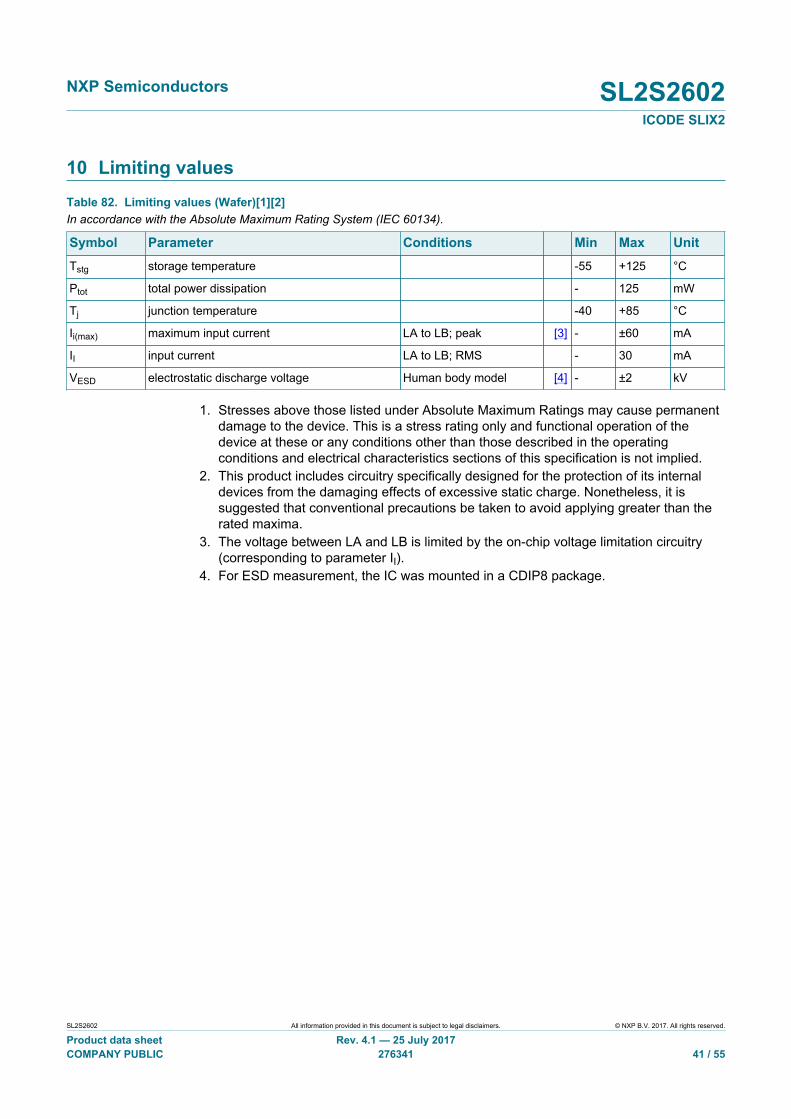
10 Limiting valuesTable 82. Limiting values (Wafer)[1][2]In accordance with the Absolute Maximum Rating System (IEC 60134).
Symbol Parameter Conditions Min Max UnitTstg storage temperature -55 +125 °C
Ptot total power dissipation - 125 mW
Tj junction temperature -40 +85 °C
Ii(max) maximum input current LA to LB; peak [3] - ±60 mA
II input current LA to LB; RMS - 30 mA
VESD electrostatic discharge voltage Human body model [4] - ±2 kV
1. Stresses above those listed under Absolute Maximum Ratings may cause permanentdamage to the device. This is a stress rating only and functional operation of thedevice at these or any conditions other than those described in the operatingconditions and electrical characteristics sections of this specification is not implied.
2. This product includes circuitry specifically designed for the protection of its internaldevices from the damaging effects of excessive static charge. Nonetheless, it issuggested that conventional precautions be taken to avoid applying greater than therated maxima.
3. The voltage between LA and LB is limited by the on-chip voltage limitation circuitry(corresponding to parameter II).
4. For ESD measurement, the IC was mounted in a CDIP8 package.

NXP Semiconductors SL2S2602ICODE SLIX2
SL2S2602 All information provided in this document is subject to legal disclaimers. © NXP B.V. 2017. All rights reserved.
Product data sheet Rev. 4.1 — 25 July 2017COMPANY PUBLIC 276341 42 / 55
11 Characteristics
11.1 Wafer memory characteristics
Table 83. Wafer EEPROM characteristicsSymbol Parameter Conditions Min Typ Max Unittret retention time Tamb ≤ 55 °C 50 - - year
Nendu(W) write endurance 100000 - - cycle
11.2 Interface characteristics
Table 84. Interface characteristicsTypical ratings are not guaranteed. The values listed are at room temperature.
Symbol Parameter Conditions Min Typ Max Unitfi input frequency [1] 13.553 13.56 13.567 MHz
Vi(RMS)min minimum RMS input voltage operating read/write
1.1 - 1.3 V
Pi(min) minimum input power operating [2] - 40 - μW
Ci input capacitance between LAand LB
[3] 22.3 23.5 24.7 pF
tpersist persistent time [4] 2 - - s
1. Bandwidth limitation (± 7 kHz) according to ISM band regulations.2. Including losses in the resonant capacitor and rectifier.3. Measured with an HP4285A LCR meter at 13.56 MHz and 1.5 V RMS.4. The maximum persistent time strongly depends on the ambient temperature.

NXP Semiconductors SL2S2602ICODE SLIX2
SL2S2602 All information provided in this document is subject to legal disclaimers. © NXP B.V. 2017. All rights reserved.
Product data sheet Rev. 4.1 — 25 July 2017COMPANY PUBLIC 276341 43 / 55
12 Marking
12.1 Marking SOT1122
Table 85. Marking SOT1122Type number Marking codeSL2S2602FTB 26

NXP Semiconductors SL2S2602ICODE SLIX2
SL2S2602 All information provided in this document is subject to legal disclaimers. © NXP B.V. 2017. All rights reserved.
Product data sheet Rev. 4.1 — 25 July 2017COMPANY PUBLIC 276341 44 / 55
13 Package outline
ReferencesOutlineversion
Europeanprojection Issue date
IEC JEDEC JEITA
SOT1122 MO-252
sot1122_po
Unit
mmmaxnommin
0.50 0.040.55 0.425
0.300.250.22
0.350.300.27
A(1)
Dimensions
Notes1. Dimension A is including plating thickness.2. Can be visible in some manufacturing processes.
SOT1122
A1 D
1.501.451.40
1.051.000.95
E e e1
0.550.500.47
0.450.400.37
b b1 L L1
09-10-09
XSON3: plastic extremely thin small outline package; no leads; 3 terminals; body 1 x 1.45 x 0.5 mm
D
E
e1
e
A1
b1
L1
L
e1
0 1 2 mm
scale
3
1
2
b
4×(2)
4×(2)
A
pin 1 indication
type code
terminal 1index area
Figure 6. Package outline SOT1122

NXP Semiconductors SL2S2602ICODE SLIX2
SL2S2602 All information provided in this document is subject to legal disclaimers. © NXP B.V. 2017. All rights reserved.
Product data sheet Rev. 4.1 — 25 July 2017COMPANY PUBLIC 276341 45 / 55
ReferencesOutlineversion
Europeanprojection Issue date
IEC JEDEC JEITA
SOT500-4 - - -- - -- - -
sot500-4_po
11-02-18
Unit
mmmaxnommin
0.26 35.0535.0034.95
A(1)
Dimensions
Note1. Total package thickness, exclusive punching burr.
PLLMC: plastic leadless module carrier package; 35 mm wide tape SOT500-4
D
For unspecified dimensions see PLLMC-drawing given in the subpackage code.
0 10 20 mm
scale
X
D
detail X
A
Figure 7. Package outline SOT500-4
For more details on the contactless MOA8 module see Ref. 9.

NXP Semiconductors SL2S2602ICODE SLIX2
SL2S2602 All information provided in this document is subject to legal disclaimers. © NXP B.V. 2017. All rights reserved.
Product data sheet Rev. 4.1 — 25 July 2017COMPANY PUBLIC 276341 46 / 55
14 Bare die outline
aaa-016467not to scale!
(1)
(7)
(2)
(8)
(5)
(6) (4)
(3)
Y
X
GND
LA LB
TEST
(9)
(10)
(1) X-scribe line width: 15 μm(2) Y-scribe line width: 15 μm(3) Chip step, X-length: 555 μm(4) Chip step, Y-length: 558 μm(5) Bump to bump distance X (LA - LB): 430 μm(6) Bump to bump distance Y (LB - TEST): 371.5 μm(7) Distance GND bump to nitride edge X: 45 μm(8) Distance GND bump to nitride edge Y: 45 μm(9) Distance LA bump to nitride edge X: 55 μm(10) Bump to bump distance X (GND - TEST): 450 μmBump size LA and LB (X × Y): 80 μm × 80 μmBump size TEST and GND (X × Y): 60 μm × 60 μmFigure 8. Wafer SL2S2602FUD/BG bare die layout

NXP Semiconductors SL2S2602ICODE SLIX2
SL2S2602 All information provided in this document is subject to legal disclaimers. © NXP B.V. 2017. All rights reserved.
Product data sheet Rev. 4.1 — 25 July 2017COMPANY PUBLIC 276341 47 / 55
15 AbbreviationsTable 86. AbbreviationsAcronym DescriptionAFI Application Family Identifier
CRC Cyclic Redundancy Check
DSFID Data Storage Format Identifier
EAS Electronic Article Surveillance
EEPROM Electrically Erasable Programmable Read Only Memory
EOF End Of Frame
IC Integrated Circuit
LCR Inductance, Capacitance, Resistance
LSB Least Significant Byte/Bit
MSB Most Significant Byte/Bit
RF Radio Frequency
SOF Start Of Frame
UID Unique IDentifier

NXP Semiconductors SL2S2602ICODE SLIX2
SL2S2602 All information provided in this document is subject to legal disclaimers. © NXP B.V. 2017. All rights reserved.
Product data sheet Rev. 4.1 — 25 July 2017COMPANY PUBLIC 276341 48 / 55
16 References
[1]
ISO Standard
ISO/IEC 15693 - Identification cards - Contactless integrated circuit cards - Vicinity cards.
[2]
ISO Standard
ISO/IEC 15693-2 -Identification cards - Contactless integrated circuit cards - Vicinitycards - Part 2: Air interface and initialization.
[3]
ISO Standard
ISO/IEC 15693-3 -Identification cards - Contactless integrated circuit cards - Vicinitycards - Part 3: Anticollision and transmission protocol.
[4]
ISO Standard
ISO/IEC 18000-3 - Information technology - Radio frequency identification for itemmanagement - Part 3: Parameters for air interface communications at 13.56 MHz.
[5]
ISO Standard
ISO/IEC 7816-6 - Identification cards - Integrated circuit cards - Part 6: Interindustry dataelements for interchange.
[6]
General specification for 8" wafer on UV-tape with electronic fail die marking
Delivery type description – BU-ID document number: 1093**1.
[7]
Certicom Research. SEC 2
Recommended Elliptic Curve Domain Parameters, version 2.0, January 2010.
[8]
Application Note
AN3660 - ICODE SLIX2 Recommended operating conditions when using 100% ASK.
[9]
Contactless smart card module specification MOA8
Delivery Type Description, BU-ID Document number 1636**1.
1 ** ... document version number

NXP Semiconductors SL2S2602ICODE SLIX2
SL2S2602 All information provided in this document is subject to legal disclaimers. © NXP B.V. 2017. All rights reserved.
Product data sheet Rev. 4.1 — 25 July 2017COMPANY PUBLIC 276341 49 / 55
17 Revision historyTable 87. Revision historyDocument ID Release date Data sheet status Change
noticeSupersedes
SL2S2602 v. 4.1 20170725 Product data sheet - SL2S2602 v. 4.0
Modifications: • Addition of SL2S2602FA8 with SOT500-4 (MOA8) package• Addition of SL2S2602FTB with SOT1122 package
SL2S2602 v. 4.0 20160218 Product data sheet - SL2S2602 v. 3.2
Modifications: • Changed ordering information to SL2S2602FUD/BG (with 7 μm Polyimide spacer)• Added 7 μm Polyimide spacer to wafer specification
SL2S2602 v. 3.2 20150126 Product data sheet - SL2S2602_276331
Modifications: • Editorial changes
SL2S2602_276331 20141210 Product data sheet - 276330
Modifications: • Security status changed into COMPANY PUBLIC
276330 20141118 Product data sheet - 276311
Modifications: • Data sheet status changed from objective to product
276311 20140528 Objective data sheet - 276310
Modifications: • Section 9.4 "State diagram" added• Conditions added for STAY QUIETPERSITANT command in Section 9.5.3.19• Modification of the QUIET and PERSISTANT QUIET bit in the extended mode of the
INVENTORY READ command in Table 47 "Extended options" and Table 48 "QUIET andPERSISTANT QUIET bit in Extended options"
• Added remark for QUIET and PERSISTANT QUIET state in Section 9.5.3.15 "EASALARM"
• Update of die dimensions in Section 8.1 "Wafer specification" and Section 14 "Bare dieoutline"
• Editorial changing
276310 20131001 Objective data sheet - -
Modifications: • Initial version

NXP Semiconductors SL2S2602ICODE SLIX2
SL2S2602 All information provided in this document is subject to legal disclaimers. © NXP B.V. 2017. All rights reserved.
Product data sheet Rev. 4.1 — 25 July 2017COMPANY PUBLIC 276341 50 / 55
18 Legal information
18.1 Data sheet status
Document status[1][2] Product status[3] Definition
Objective [short] data sheet Development This document contains data from the objective specification for productdevelopment.
Preliminary [short] data sheet Qualification This document contains data from the preliminary specification.
Product [short] data sheet Production This document contains the product specification.
[1] Please consult the most recently issued document before initiating or completing a design.[2] The term 'short data sheet' is explained in section "Definitions".[3] The product status of device(s) described in this document may have changed since this document was published and may differ in case of multiple
devices. The latest product status information is available on the Internet at URL http://www.nxp.com.
18.2 DefinitionsDraft — The document is a draft version only. The content is still underinternal review and subject to formal approval, which may result inmodifications or additions. NXP Semiconductors does not give anyrepresentations or warranties as to the accuracy or completeness ofinformation included herein and shall have no liability for the consequencesof use of such information.
Short data sheet — A short data sheet is an extract from a full data sheetwith the same product type number(s) and title. A short data sheet isintended for quick reference only and should not be relied upon to containdetailed and full information. For detailed and full information see therelevant full data sheet, which is available on request via the local NXPSemiconductors sales office. In case of any inconsistency or conflict with theshort data sheet, the full data sheet shall prevail.
Product specification — The information and data provided in a Productdata sheet shall define the specification of the product as agreed betweenNXP Semiconductors and its customer, unless NXP Semiconductors andcustomer have explicitly agreed otherwise in writing. In no event however,shall an agreement be valid in which the NXP Semiconductors productis deemed to offer functions and qualities beyond those described in theProduct data sheet.
18.3 DisclaimersLimited warranty and liability — Information in this document is believedto be accurate and reliable. However, NXP Semiconductors does notgive any representations or warranties, expressed or implied, as to theaccuracy or completeness of such information and shall have no liabilityfor the consequences of use of such information. NXP Semiconductorstakes no responsibility for the content in this document if provided by aninformation source outside of NXP Semiconductors. In no event shall NXPSemiconductors be liable for any indirect, incidental, punitive, special orconsequential damages (including - without limitation - lost profits, lostsavings, business interruption, costs related to the removal or replacementof any products or rework charges) whether or not such damages are basedon tort (including negligence), warranty, breach of contract or any otherlegal theory. Notwithstanding any damages that customer might incur forany reason whatsoever, NXP Semiconductors’ aggregate and cumulativeliability towards customer for the products described herein shall be limitedin accordance with the Terms and conditions of commercial sale of NXPSemiconductors.
Right to make changes — NXP Semiconductors reserves the right tomake changes to information published in this document, including withoutlimitation specifications and product descriptions, at any time and withoutnotice. This document supersedes and replaces all information supplied priorto the publication hereof.
Suitability for use — NXP Semiconductors products are not designed,authorized or warranted to be suitable for use in life support, life-critical orsafety-critical systems or equipment, nor in applications where failure ormalfunction of an NXP Semiconductors product can reasonably be expectedto result in personal injury, death or severe property or environmentaldamage. NXP Semiconductors and its suppliers accept no liability forinclusion and/or use of NXP Semiconductors products in such equipment orapplications and therefore such inclusion and/or use is at the customer’s ownrisk.
Applications — Applications that are described herein for any of theseproducts are for illustrative purposes only. NXP Semiconductors makesno representation or warranty that such applications will be suitablefor the specified use without further testing or modification. Customersare responsible for the design and operation of their applications andproducts using NXP Semiconductors products, and NXP Semiconductorsaccepts no liability for any assistance with applications or customer productdesign. It is customer’s sole responsibility to determine whether the NXPSemiconductors product is suitable and fit for the customer’s applicationsand products planned, as well as for the planned application and use ofcustomer’s third party customer(s). Customers should provide appropriatedesign and operating safeguards to minimize the risks associated withtheir applications and products. NXP Semiconductors does not accept anyliability related to any default, damage, costs or problem which is basedon any weakness or default in the customer’s applications or products, orthe application or use by customer’s third party customer(s). Customer isresponsible for doing all necessary testing for the customer’s applicationsand products using NXP Semiconductors products in order to avoid adefault of the applications and the products or of the application or use bycustomer’s third party customer(s). NXP does not accept any liability in thisrespect.
Limiting values — Stress above one or more limiting values (as defined inthe Absolute Maximum Ratings System of IEC 60134) will cause permanentdamage to the device. Limiting values are stress ratings only and (proper)operation of the device at these or any other conditions above thosegiven in the Recommended operating conditions section (if present) or theCharacteristics sections of this document is not warranted. Constant orrepeated exposure to limiting values will permanently and irreversibly affectthe quality and reliability of the device.
Terms and conditions of commercial sale — NXP Semiconductorsproducts are sold subject to the general terms and conditions of commercialsale, as published at http://www.nxp.com/profile/terms, unless otherwiseagreed in a valid written individual agreement. In case an individualagreement is concluded only the terms and conditions of the respectiveagreement shall apply. NXP Semiconductors hereby expressly objects toapplying the customer’s general terms and conditions with regard to thepurchase of NXP Semiconductors products by customer.
No offer to sell or license — Nothing in this document may be interpretedor construed as an offer to sell products that is open for acceptance orthe grant, conveyance or implication of any license under any copyrights,patents or other industrial or intellectual property rights.

NXP Semiconductors SL2S2602ICODE SLIX2
SL2S2602 All information provided in this document is subject to legal disclaimers. © NXP B.V. 2017. All rights reserved.
Product data sheet Rev. 4.1 — 25 July 2017COMPANY PUBLIC 276341 51 / 55
Quick reference data — The Quick reference data is an extract of theproduct data given in the Limiting values and Characteristics sections of thisdocument, and as such is not complete, exhaustive or legally binding.
Export control — This document as well as the item(s) described hereinmay be subject to export control regulations. Export might require a priorauthorization from competent authorities.
Non-automotive qualified products — Unless this data sheet expresslystates that this specific NXP Semiconductors product is automotive qualified,the product is not suitable for automotive use. It is neither qualified nortested in accordance with automotive testing or application requirements.NXP Semiconductors accepts no liability for inclusion and/or use of non-automotive qualified products in automotive equipment or applications. Inthe event that customer uses the product for design-in and use in automotiveapplications to automotive specifications and standards, customer (a) shalluse the product without NXP Semiconductors’ warranty of the product forsuch automotive applications, use and specifications, and (b) whenever
customer uses the product for automotive applications beyond NXPSemiconductors’ specifications such use shall be solely at customer’s ownrisk, and (c) customer fully indemnifies NXP Semiconductors for any liability,damages or failed product claims resulting from customer design and useof the product for automotive applications beyond NXP Semiconductors’standard warranty and NXP Semiconductors’ product specifications.
Translations — A non-English (translated) version of a document is forreference only. The English version shall prevail in case of any discrepancybetween the translated and English versions.
18.4 TrademarksNotice: All referenced brands, product names, service names andtrademarks are the property of their respective owners.
ICODE and I-CODE — are trademarks of NXP B.V.

NXP Semiconductors SL2S2602ICODE SLIX2
SL2S2602 All information provided in this document is subject to legal disclaimers. © NXP B.V. 2017. All rights reserved.
Product data sheet Rev. 4.1 — 25 July 2017COMPANY PUBLIC 276341 52 / 55
TablesTab. 1. Ordering information ..........................................5Tab. 2. Pin description SOT1122 .................................. 7Tab. 3. Pin description SOT500-4 (MOA8) ....................7Tab. 4. Bonding pad description ....................................8Tab. 5. Wafer specification ............................................9Tab. 6. Memory organization .......................................12Tab. 7. Unique identifier .............................................. 12Tab. 8. Type indicator bits ...........................................12Tab. 9. GET RANDOM NUMBER request format ........17Tab. 10. GET RANDOM NUMBER response when
Error_flag set ...................................................18Tab. 11. GET RANDOM NUMBER response format
when Error_flag NOT set ................................ 18Tab. 12. SET PASSWORD request format ................... 18Tab. 13. Password Identifier ..........................................18Tab. 14. SET PASSWORD response format when
Error_flag set ...................................................19Tab. 15. SET PASSWORD response format when
Error_flag NOT set ..........................................19Tab. 16. WRITE PASSWORD request format ...............19Tab. 17. Password Identifier ..........................................19Tab. 18. WRITE PASSWORD response format when
Error_flag set ...................................................20Tab. 19. WRITE PASSWORD response format when
Error_flag NOT set ..........................................20Tab. 20. LOCK PASSWORD request format ................ 20Tab. 21. Password identifier ..........................................20Tab. 22. LOCK PASSWORD response format when
Error_flag set ...................................................20Tab. 23. LOCK PASSWORD response format when
Error_flag NOT set ..........................................21Tab. 24. 64 BIT PASSWORD PROTECTION request
format .............................................................. 21Tab. 25. 64 BIT PASSWORD PROTECTION
response format when Error_flag set .............. 21Tab. 26. 64 BIT PASSWORD PROTECTION
response format when Error_flag NOT set ......21Tab. 27. Memory organization .......................................22Tab. 28. POTECT PAGE request format .......................22Tab. 29. Extended Protection status byte ......................22Tab. 30. Protection status bits definition ....................... 23Tab. 31. POTECT PAGE response format when
Error_flag set ...................................................23Tab. 32. POTECT PAGE response format when
Error_flag NOT set ..........................................23Tab. 33. LOCK PAGE PROTECTION CONDITION
request format ................................................. 24Tab. 34. LOCK PAGE PROTECTION CONDITION
response format when Error_flag set .............. 24Tab. 35. LOCK PAGE PROTECTION CONDITION
response format when Error_flag NOT set ......24Tab. 36. DESTROY request format ...............................24Tab. 37. DESTROY response format when Error_flag
set ....................................................................25Tab. 38. DESTROY response format when Error_flag
NOT set ...........................................................25
Tab. 39. ENABLE PRIVACY request format ................. 25Tab. 40. ENABLE PRIVACY response format when
Error_flag set ...................................................25Tab. 41. ENABLE PRIVACY response format when
Error_flag NOT set ..........................................25Tab. 42. INVENTORY READ request format ................ 26Tab. 43. INVENTORY READ response format:
Option flag logic 0 ...........................................27Tab. 44. INVENTORY READ response format:
Option flag logic 1 ...........................................27Tab. 45. Example: mask length = 30 ............................ 27Tab. 46. Inventory Read (extended mode) response
format .............................................................. 28Tab. 47. Extended options ............................................ 28Tab. 48. QUIET and PERSISTANT QUIET bit in
Extended options ............................................ 29Tab. 49. Inventory Read (extended mode) response
format: Option flag logic 1 ...............................29Tab. 50. Example ...........................................................29Tab. 51. SET EAS request format .................................30Tab. 52. SET EAS response format when Error_flag
set ....................................................................30Tab. 53. SET EAS response format when Error_flag
NOT set ...........................................................30Tab. 54. RESET EAS request format ............................31Tab. 55. RESET EAS response format when
Error_flag set ...................................................31Tab. 56. RESET EAS response format when
Error_flag NOT set ..........................................31Tab. 57. LOCK EAS request format ..............................31Tab. 58. LOCK EAS response format when
Error_flag set ...................................................31Tab. 59. LOCK EAS response format when
Error_flag NOT set ..........................................32Tab. 60. EAS ALARM Request format .......................... 32Tab. 61. EAS ALARM Response format (Option flag
logic 0) ............................................................ 32Tab. 62. EAS ALARM Response format (Option flag
logic 1) ............................................................ 32Tab. 63. PASSWORD PROTECT EAS/AFI request
format .............................................................. 33Tab. 64. PASSWORD PROTECT EAS/AFI response
format when Error_flag set ..............................33Tab. 65. PASSWORD PROTECT EAS/AFI response
format when Error_flag NOT set ..................... 33Tab. 66. WRITE EAS ID request format ........................34Tab. 67. WRITE EAS ID response format when
Error_flag set ...................................................34Tab. 68. WRITE EAS ID response format when
Error_flag NOT set ..........................................34Tab. 69. GET NXP SYSTEM INFORMATION request
format .............................................................. 34Tab. 70. GET NXP SYSTEM INFORMATION
response format when Error_flag set .............. 34Tab. 71. GET NXP SYSTEM INFORMATION
response format when Error_flag NOT set ......34

NXP Semiconductors SL2S2602ICODE SLIX2
SL2S2602 All information provided in this document is subject to legal disclaimers. © NXP B.V. 2017. All rights reserved.
Product data sheet Rev. 4.1 — 25 July 2017COMPANY PUBLIC 276341 53 / 55
Tab. 72. PP conditions bits ........................................... 35Tab. 73. Lock bits ..........................................................35Tab. 74. Feature flags bits ............................................ 35Tab. 75. STAY PERSISTENT QUIET request format ....36Tab. 76. READ SIGNATURE request format ................ 37Tab. 77. READ SIGNATURE response format when
Error_flag set ...................................................37Tab. 78. READ SIGNATURE response format when
Error_flag NOT set ..........................................37
Tab. 79. COUNTER BLOCK data structure .................. 37Tab. 80. Preset counter data structure ..........................38Tab. 81. Increment counter data structure .................... 38Tab. 82. Limiting values (Wafer)[1][2] ............................41Tab. 83. Wafer EEPROM characteristics ...................... 42Tab. 84. Interface characteristics .................................. 42Tab. 85. Marking SOT1122 ........................................... 43Tab. 86. Abbreviations ...................................................47Tab. 87. Revision history ...............................................49

NXP Semiconductors SL2S2602ICODE SLIX2
SL2S2602 All information provided in this document is subject to legal disclaimers. © NXP B.V. 2017. All rights reserved.
Product data sheet Rev. 4.1 — 25 July 2017COMPANY PUBLIC 276341 54 / 55
FiguresFig. 1. Block diagram of ICODE SLIX2 ........................ 6Fig. 2. Pin configuration for SOT1122 ..........................7Fig. 3. Pin configuration for SOT500-4 (MOA8) ........... 7Fig. 4. Wafer SL2S2602FUD/BG layout and pin
configuration for the bare die ............................ 8
Fig. 5. State diagram ICODE SLIX2 ...........................14Fig. 6. Package outline SOT1122 .............................. 44Fig. 7. Package outline SOT500-4 ............................. 45Fig. 8. Wafer SL2S2602FUD/BG bare die layout ....... 46

NXP Semiconductors SL2S2602ICODE SLIX2
Please be aware that important notices concerning this document and the product(s)described herein, have been included in section 'Legal information'.
© NXP B.V. 2017. All rights reserved.For more information, please visit: http://www.nxp.comFor sales office addresses, please send an email to: [email protected]
Date of release: 25 July 2017Document identifier: SL2S2602
Document number: 276341
Contents1 General description ............................................ 11.1 Contactless energy and data transfer ................11.2 Anticollision ........................................................ 11.3 Security and privacy aspects .............................12 Features and benefits .........................................32.1 ICODE SLIX2 RF interface (ISO/IEC 15693) .....32.2 EEPROM ........................................................... 32.3 Security ..............................................................33 Applications .........................................................44 Ordering information .......................................... 55 Block diagram ..................................................... 66 Pinning information ............................................ 77 Wafer Layout ....................................................... 87.1 Pin Description .................................................. 88 Mechanical specification ....................................98.1 Wafer specification ............................................ 98.1.1 Fail die identification ........................................108.1.2 Map file distribution ......................................... 109 Functional description ......................................119.1 Block description ............................................. 119.2 Memory organization ....................................... 119.2.1 Unique identifier ...............................................129.2.2 Originality signature .........................................139.2.3 Configuration of delivered ICs ......................... 139.3 Communication principle ................................. 149.4 State diagram .................................................. 149.5 Supported commands ......................................159.5.1 Mandatory commands ..................................... 159.5.1.1 INVENTORY .................................................... 159.5.1.2 STAY QUIET ................................................... 159.5.2 Optional commands .........................................159.5.2.1 READ SINGLE BLOCK ................................... 159.5.2.2 WRITE SINGLE BLOCK ..................................159.5.2.3 LOCK BLOCK ..................................................159.5.2.4 READ MULTIPLE BLOCKS .............................169.5.2.5 SELECT ...........................................................169.5.2.6 RESET TO READY ......................................... 169.5.2.7 WRITE AFI ...................................................... 169.5.2.8 LOCK AFI ........................................................ 169.5.2.9 WRITE DSFID ................................................. 179.5.2.10 LOCK DSFID ................................................... 179.5.2.11 GET SYSTEM INFORMATION ....................... 179.5.2.12 GET MULTIPLE BLOCK SECURITY
STATUS ...........................................................179.5.3 Custom commands ..........................................179.5.3.1 GET RANDOM NUMBER ................................179.5.3.2 SET PASSWORD ............................................189.5.3.3 WRITE PASSWORD ....................................... 199.5.3.4 LOCK PASSWORD ......................................... 209.5.3.5 64 BIT PASSWORD PROTECTION ................219.5.3.6 PROTECT PAGE .............................................219.5.3.7 LOCK PAGE PROTECTION CONDITION .......239.5.3.8 DESTROY ........................................................24
9.5.3.9 ENABLE PRIVACY ..........................................259.5.3.10 INVENTORY READ .........................................259.5.3.11 FAST INVENTORY READ ...............................309.5.3.12 SET EAS ......................................................... 309.5.3.13 RESET EAS .................................................... 319.5.3.14 LOCK EAS .......................................................319.5.3.15 EAS ALARM .................................................... 329.5.3.16 PASSWORD PROTECT EAS/AFI ................... 339.5.3.17 WRITE EAS ID ................................................ 339.5.3.18 GET NXP SYSTEM INFOMATION ..................349.5.3.19 STAY QUIET PERSISTENT ............................369.5.3.20 READ SIGNATURE .........................................379.5.3.21 16 bit Counter ..................................................379.6 Error handling .................................................. 399.6.1 Transmission errors .........................................399.6.2 Not supported commands or options ...............399.6.2.1 Non Addressed Mode ......................................399.6.2.2 Addressed or Selected Mode .......................... 399.6.3 Parameter out of range ................................... 399.6.3.1 Read commands ............................................. 399.6.3.2 Write and lock commands ............................... 399.7 Data integrity ................................................... 409.8 RF interface ..................................................... 4010 Limiting values ..................................................4111 Characteristics .................................................. 4211.1 Wafer memory characteristics ......................... 4211.2 Interface characteristics ...................................4212 Marking ...............................................................4312.1 Marking SOT1122 ............................................4313 Package outline .................................................4414 Bare die outline .................................................4615 Abbreviations .................................................... 4716 References ......................................................... 4817 Revision history ................................................ 4918 Legal information ..............................................50