iC-PT3310 6-CH. PHASED ARRAY OPTO ENCODER … rr e lliim in aa r y iC-PT3310 6-CH. PHASED ARRAY OPTO...
12
preliminary preliminary iC-PT 3310 6-CH. PHASED ARRAY OPTO ENCODER (33-1000) Rev B2, Page 1/12 FEATURES ♦ Monolithic photodiode array with excellent signal matching ♦ Very compact size for small encoders ♦ Moderate track pitch for relaxed assembly tolerances ♦ Low noise signal amplifiers with high EMI tolerance ♦ Single-pin programming of 3 operating modes: analog, digital (1000 CPR), and x2 interpolated (2000 CPR) ♦ Analog signals for alignment and resolution enhancement ♦ Selectable index gating: 1 T, 0.5 T (B-gated), 0.25 T (AB-gated) ♦ Complementary outputs: A, B, Z and NA, NB, NZ ♦ Up to 50,000 RPM at 1000 CPR (25,000 RPM at 2000 CPR) ♦ U, V, W commutation signals (digital/analog) ♦ All outputs +/- 4 mA push-pull, current-limited and short-circuit-proof ♦ LED power control with 40 mA high-side driver ♦ Single 3.5 V to 5.5 V operation, low power consumption ♦ Operating temperature range of -40 °C to +110 °C (+120 °C) ♦ Code disc available: PT2S 33-1000 (glass 1 mm) OD ∅33.2 mm, ID ∅13.0 mm, optical radius 14.5 mm, 1000 ppr and 3 ppr commutation (120°) APPLICATIONS ♦ Incremental encoder ♦ Brushless DC motor commutation ♦ Industrial drives PACKAGES optoQFN32-5x5 5 mm x 5 mm x 0.9 mm BLOCK DIAGRAM POWER CONTROL iC-PT PB PA NZ U V OUTPUT COMPARATION SIGNAL OUTPUT AND W PZ COMMUTATION QUADRATURE POWER-ON RESET INDEX NB NA LED D1 1μF C1 + - R1 47 +3.5..5.5V T1 CA W V TIP TIN U LED PA NZ PZ NB PB NA SEL GND VCC D1 C1 1μF 47 R1 Copyright © 2009, 2012 iC-Haus http://www.ichaus.com
Transcript of iC-PT3310 6-CH. PHASED ARRAY OPTO ENCODER … rr e lliim in aa r y iC-PT3310 6-CH. PHASED ARRAY OPTO...
preliminary preliminary iC-PT 33106-CH. PHASED ARRAY OPTO ENCODER (33-1000)
Rev B2, Page 1/12
FEATURES
♦ Monolithic photodiode array with excellent signal matching
♦ Very compact size for small encoders
♦ Moderate track pitch for relaxed assembly tolerances
♦ Low noise signal amplifiers with high EMI tolerance
♦ Single-pin programming of 3 operating modes:
analog, digital (1000 CPR), and x2 interpolated (2000 CPR)
♦ Analog signals for alignment and resolution enhancement
♦ Selectable index gating: 1 T, 0.5 T (B-gated), 0.25 T (AB-gated)
♦ Complementary outputs: A, B, Z and NA, NB, NZ
♦ Up to 50,000 RPM at 1000 CPR (25,000 RPM at 2000 CPR)
♦ U, V, W commutation signals (digital/analog)
♦ All outputs +/- 4 mA push-pull, current-limited and
short-circuit-proof
♦ LED power control with 40 mA high-side driver
♦ Single 3.5 V to 5.5 V operation, low power consumption
♦ Operating temperature range of -40 °C to +110 °C (+120 °C)
♦ Code disc available: PT2S 33-1000 (glass 1 mm)
OD ∅33.2 mm, ID ∅13.0 mm, optical radius 14.5 mm,
1000 ppr and 3 ppr commutation (120°)
APPLICATIONS
♦ Incremental encoder
♦ Brushless DC motor
commutation
♦ Industrial drives
PACKAGES
optoQFN32-5x5
5 mm x 5 mm x 0.9 mm
BLOCK DIAGRAM
POWERCONTROL
iC-PT
PB
PA
NZ
U
V
OUTPUT
COMPARATIONSIGNAL
OUTPUT
AND
W
PZ
COMMUTATION
QUADRATURE
POWER-ON RESET
INDEX
NB
NA
LED
D1
1μFC1
+-
R147
+3.5..5.5V
T1
CAW
V
TIP TIN
U
LED
PA
NZ
PZ
NBPB
NA
SEL
GND
VCC
D1
C11μF
47R1
Copyright © 2009, 2012 iC-Haus http://www.ichaus.com

preliminary preliminary iC-PT 33106-CH. PHASED ARRAY OPTO ENCODER (33-1000)
Rev B2, Page 2/12
DESCRIPTION
iC-PT 3310 is an optical sensor IC with integrated
photosensors whose signals are converted into volt-
ages by low-noise transimpedance amplifiers. Pre-
cise voltage comparators with hysteresis are used to
generate the digital signals, supplied to the output
pins via differential +/- 4 mA push-pull drivers.
The built-in LED power control with its 40 mA driver
stage permits a direct connection of the encoder
LED. Regardless of aging or changes in temperature
the received optical power is kept constant.
Selection input SEL chooses for three different op-
erating modes: regular A/B operation, A/B operation
with 2-fold interpolation, or analog operation. With
analog operation the amplified signal voltages are
available at the outputs for inspection and monitoring
encoder assembly.
Typical applications of iC-PT devices are incremental
encoders for motor feedback and commutation. To
this end, device version iC-PT 3310 provides differ-
ential A/B tracks and a differential index track, each
consisting of multiple photo sensors. The layout of
the signal amplifiers is such that there is an excellent
paired channel matching, eliminating the needs for
signal calibration in most cases.
Additionally, three more tracks are provided to gener-
ate motor commutation information for the U, V and
W outputs, for instance with 120 degree phase shift
to operate 3-phase brushless motors (period count
and phase shift can be varied by the code disc ap-
plied).

preliminary preliminary iC-PT 33106-CH. PHASED ARRAY OPTO ENCODER (33-1000)
Rev B2, Page 3/12
PACKAGING INFORMATION
PAD LAYOUT
Chip size 2.88 mm x 3.37 mm
PAD FUNCTIONS
No. Name Function
See pin configuration.
PIN CONFIGURATION
oQFN32-5x5, -3 (5 mm x 5 mm)
12345678
9 10 11 12 13 14 15 16
1718192021222324
2526272829303132
PIN FUNCTIONS
No. Name Function
1 VCC +3.5..5.5 V Supply Voltage
2 LED LED Controller, High-Side Current
Source Output
3 PA Push-Pull Output A+ / Analog Sin+ 1)
4 NA Push-Pull Output A- / Analog Sin-
5 PB Push-Pull Output B+ / Analog Cos+
6 NB Push-Pull Output B- / Analog Cos-
7 PZ Push-Pull Output Z+ / Analog Z+
8 NZ Push-Pull Output Z- / Analog Z-
9..16 n.c.2)
17 SEL Op. Mode Selection Input:
lo = digital
hi = x2 interpolated
open = analog (alignment aid)
18 W Push-Pull Output W / Analog W
19 TIN Negative Test Current Input 3)
20 V Push-Pull Output V / Analog V
21 TIP Positive Test Current Input 3)
22 U Push-Pull Output U / Analog U
23 T1 Index Length Selection Input:
lo = 0.5 T (B-gated),
hi = 1 T (ungated/T-gated),
open = 0.25 T (A and B-gated)
24 GND Ground
25..32 n.c.
BP Backside Paddle 4)
1) Capacitive pin loads must be avoided when using the analog output signals.2) Pin numbers marked n.c. are not in use.3) The test pins TIP and TIN may remain unconnected.4) The backside paddle may have a single link to GND. A current flow across the paddle is not permissible.
preliminary preliminary iC-PT 33106-CH. PHASED ARRAY OPTO ENCODER (33-1000)
Rev B2, Page 4/12
PACKAGE DIMENSIONS
All dimensions given in mm.
Maximum molding excess +20 µm / -200 µm versus surface of glass.
5
5
1.90
3.24
TOP
0.90
0.30 SIDE
3.603.60
0.50 0.23 0.40
BOTTOM
3.60
3.60
0.50 0.30
4.90
4.90
R0.15
0.70
RECOMMENDED PCB-FOOTPRINT
dra_pt33xx-oqfn32-2_pack_1, 10:1
preliminary preliminary iC-PT 33106-CH. PHASED ARRAY OPTO ENCODER (33-1000)
Rev B2, Page 5/12
ABSOLUTE MAXIMUM RATINGS
These ratings do not imply operating conditions; functional operation is not guaranteed. Beyond these ratings device damage may occur.
Item Symbol Parameter Conditions UnitNo. Min. Max.
G001 VCC Voltage at VCC -0.3 6 V
G002 I(VCC) Current in VCC -20 20 mA
G003 V() Voltage at Output Pins
PA, NA, PB, NB, PZ, NZ, U, V, W
-0.3 VCC +
0.3
V
G004 I() Current in Output Pins
PA, NA, PB, NB, PZ, NZ, U, V, W
-20 20 mA
G005 V() Voltage at LED -0.3 VCC +
0.3
V
G006 I() Current in LED -120 20 mA
G007 V() Voltage at TIP, TIN, SEL -0.3 VCC +
0.3
V
G008 I() Current in TIP, TIN, SEL -20 20 mA
G009 Vd() ESD Susceptibility, all pins HBM, 100 pF discharged through 1.5 kΩ 2 kV
G010 Tj Junction Temperature -40 150 °C
G011 Ts Chip Storage Temperature Range -40 150 °C
THERMAL DATA
Item Symbol Parameter Conditions UnitNo. Min. Typ. Max.
T01 Ta Operating Ambient Temperature Range
(extended range on request)
-40 110 °C
T02 Ts Permissible Storage Temperature
Range
-40 110 °C
T03 Tpk Soldering Peak Temperature tpk < 20 s, convection reflow 245 °Ctpk < 20 s, vapor phase soldering 230 °C
MSL 5A (max. floor live 24 h at 30 °C and
60 % RH);Please refer to customer information file No. 7
for details.
All voltages are referenced to ground unless otherwise stated.
All currents flowing into the device pins are positive; all currents flowing out of the device pins are negative.
preliminary preliminary iC-PT 33106-CH. PHASED ARRAY OPTO ENCODER (33-1000)
Rev B2, Page 6/12
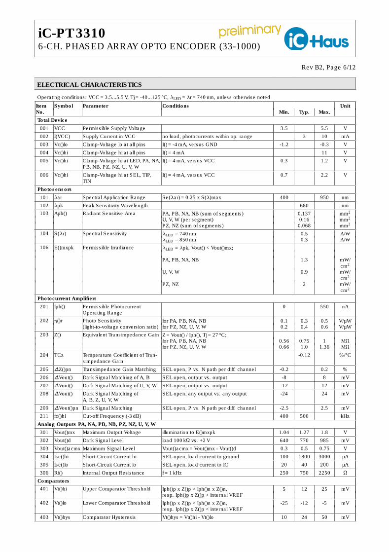
ELECTRICAL CHARACTERISTICS
Operating conditions: VCC = 3.5...5.5 V, Tj = -40...125 °C, λLED = λr = 740 nm, unless otherwise noted
Item Symbol Parameter Conditions UnitNo. Min. Typ. Max.
Total Device
001 VCC Permissible Supply Voltage 3.5 5.5 V
002 I(VCC) Supply Current in VCC no load, photocurrents within op. range 3 10 mA
003 Vc()lo Clamp-Voltage lo at all pins I() = -4 mA, versus GND -1.2 -0.3 V
004 Vc()hi Clamp-Voltage hi at all pins I() = 4 mA 11 V
005 Vc()hi Clamp-Voltage hi at LED, PA, NA,
PB, NB, PZ, NZ, U, V, W
I() = 4 mA, versus VCC 0.3 1.2 V
006 Vc()hi Clamp-Voltage hi at SEL, TIP,
TIN
I() = 4 mA, versus VCC 0.7 2.2 V
Photosensors
101 λar Spectral Application Range Se(λar) = 0.25 x S(λ)max 400 950 nm
102 λpk Peak Sensitivity Wavelength 680 nm
103 Aph() Radiant Sensitive Area PA, PB, NA, NB (sum of segments) 0.137 mm2
U, V, W (per segment) 0.16 mm2
PZ, NZ (sum of segments) 0.068 mm2
104 S(λr) Spectral Sensitivity λLED = 740 nm 0.5 A/WλLED = 850 nm 0.3 A/W
106 E()mxpk Permissible Irradiance λLED = λpk, Vout() < Vout()mx;
PA, PB, NA, NB 1.3 mW/
cm2
U, V, W 0.9 mW/
cm2
PZ, NZ 2 mW/
cm2
Photocurrent Amplifiers
201 Iph() Permissible Photocurrent
Operating Range
0 550 nA
202 η()r Photo Sensitivity
(light-to-voltage conversion ratio)for PA, PB, NA, NB 0.1 0.3 0.5 V/µWfor PZ, NZ, U, V, W 0.2 0.4 0.6 V/µW
203 Z() Equivalent Transimpedance Gain Z = Vout() / Iph(), Tj = 27 °C;for PA, PB, NA, NB 0.56 0.75 1 MΩfor PZ, NZ, U, V, W 0.66 1.0 1.36 MΩ
204 TCz Temperature Coefficient of Tran-
simpedance Gain
-0.12 %/°C
205 ∆Z()pn Transimpedance Gain Matching SEL open, P vs. N path per diff. channel -0.2 0.2 %
206 ∆Vout() Dark Signal Matching of A, B SEL open, output vs. output -8 8 mV
207 ∆Vout() Dark Signal Matching of U, V, W SEL open, output vs. output -12 12 mV
208 ∆Vout() Dark Signal Matching of
A, B, Z, U, V, W
SEL open, any output vs. any output -24 24 mV
209 ∆Vout()pn Dark Signal Matching SEL open, P vs. N path per diff. channel -2.5 2.5 mV
211 fc()hi Cut-off Frequency (-3 dB) 400 500 kHz
Analog Outputs PA, NA, PB, NB, PZ, NZ, U, V, W
301 Vout()mx Maximum Output Voltage illumination to E()mxpk 1.04 1.27 1.8 V
302 Vout()d Dark Signal Level load 100 kΩ vs. +2 V 640 770 985 mV
303 Vout()acmx Maximum Signal Level Vout()acmx = Vout()mx - Vout()d 0.3 0.5 0.75 V
304 Isc()hi Short-Circuit Current hi SEL open, load current to ground 100 1800 3000 µA
305 Isc()lo Short-Circuit Current lo SEL open, load current to IC 20 40 200 µA
306 Ri() Internal Output Resistance f = 1 kHz 250 750 2250 Ω
Comparators
401 Vt()hi Upper Comparator Threshold Iph()p x Z()p > Iph()n x Z()n, 5 12 25 mVresp. Iph()p x Z()p > internal VREF
402 Vt()lo Lower Comparator Threshold Iph()p x Z()p < Iph()n x Z()n, -25 -12 -5 mVresp. Iph()p x Z()p < internal VREF
403 Vt()hys Comparator Hysteresis Vt()hys = Vt()hi - Vt()lo 10 24 50 mV

preliminary preliminary iC-PT 33106-CH. PHASED ARRAY OPTO ENCODER (33-1000)
Rev B2, Page 7/12
ELECTRICAL CHARACTERISTICS
Operating conditions: VCC = 3.5...5.5 V, Tj = -40...125 °C, λLED = λr = 740 nm, unless otherwise noted
Item Symbol Parameter Conditions UnitNo. Min. Typ. Max.
LED Power Control
501 Iop() Permissible LED Output Current -40 0 mA
502 Vs()hi Saturation Voltage hi Vs()hi = VCC - V(LED); I() = -40 mA 0.25 0.5 1 V
503 Isc()hi Short-Circuit Current hi V() = 0 V -150 -50 mA
Digital Outputs PA, NA, PB, NB, PZ, NZ, U, V, W
601 fout Maximum Output Frequency 800 kHz
602 Vs()lo Saturation Voltage lo VCC = 4.5...5.5 V, I() = 4mA, Tj = 70 °C 0.4 V
603 Vs()lo Saturation Voltage lo VCC = 4.5...5.5 V, I() = 4mA, Tj = 85 °C 0.5 V
604 Vs()lo Saturation Voltage lo VCC = 3.5...4.5 V, I() = 4mA 0.6 V
605 Isc()lo Short-Circuit Current lo V() = VCC 7 70 mA
606 Vs()hi Saturation Voltage hi Vs()hi = VCC - V(), I() = -4 mA;VCC = 4.5...5.5 V 0.4 VVCC = 3.5...4.5 V 0.6 V
607 Isc()hi Short-Circuit Current hi V() = 0 V -70 -7 mA
Selection Input SEL
701 Vt1()hi Upper Threshold Voltage hi for A/B mode with x2 interpolation 78 80 82 %VCC
702 Vt1()lo Upper Threshold Voltage lo for A/B mode with x2 interpolation 68 70 72 %VCC
703 Vt1()hys Upper Threshold Hysteresis Vt1()hys = Vt1()hi - Vt1()lo 8 10 12 %VCC
704 Vt2()hi Lower Threshold Voltage hi for A/B mode 28 30 32 %VCC
705 Vt2()lo Lower Threshold Voltage lo for A/B mode 18 20 22 %VCC
706 Vt2()hys Lower Threshold Hysteresis Vt2()hys = Vt2()hi - Vt2()lo 8 10 12 %VCC
707 V0() Pin-Open Voltage for analog mode 45 50 55 %VCC
708 Rpd() Pull-Down Resistor SEL to GND, V(SEL) = VCC 70 100 140 kΩ
709 Rpu() Pull-Up Resistor VCC to SEL, V(SEL) = 0 V 70 100 140 kΩ
710 Vpd() Pull-Down Voltage vs. VCC/2 Vpd() = V() - VCC/2; I() = 0...5 µA 0.5 V
711 Vpu() Pull-Up Voltage vs. VCC/2 Vpu() = V() - VCC/2; I() = -5...0 µA -0.5 V
Test Circuit Inputs TIP, TIN
801 I()test Permissible Test Current Range test mode active 10 600 µA
802 V()test Test Pin Voltage test mode active, I() = 200 µA 1.25 1.5 1.75 V
803 Ipd() Test Pin Pull-Down Current test mode not active, V() = 0.4 V 60 100 160 µA
804 Ipd() Test Pin Pull-Down Current V() = VCC 0.7 2 3 mA
805 It()on Test Mode Activation Threshold 80 130 190 µA
806 CR() Test Mode Current Ratio I()/Iph() test mode active, I() = 200 µA 1500 3000 5000
Power-On-Reset Circuit
901 VCCon Turn-on Threshold VCC
(power-on release)
increasing voltage at VCC 2.6 3.45 V
902 VCCoff Turn-off Threshold VCC
(power-down reset)
decreasing voltage at VCC 1.4 2.4 V
903 VCChys Threshold Hysteresis VCChys = VCCon - VCCoff 50 170 300 mV
Index Length Selection Input T1
A01 Vt1()hi Upper Threshold Voltage hi for index length 1 T 78 80 82 %VCC
A02 Vt1()lo Upper Threshold Voltage lo for index length 1 T 68 70 72 %VCC
A03 Vt1()hys Upper Threshold Hysteresis Vt1()hys = Vt1()hi - Vt1()lo 8 10 12 %VCC
A04 Vt2()hi Lower Threshold Voltage hi for index length 0.5 T (B-gated) 28 30 32 %VCC
A05 Vt2()lo Lower Threshold Voltage lo for index length 0.5 T (B-gated) 18 20 22 %VCC
A06 Vt2()hys Lower Threshold Hysteresis Vt2()hys = Vt2()hi - Vt2()lo 8 10 12 %VCC
A07 V0() Pin-Open Voltage for index length 0.25 T (AB-gated) 45 50 55 %VCC
A08 Rpu() Pull-Up Resistor VCC to T1, V(T1) = 0 V 70 100 140 kΩ
A09 Rpd() Pull-Down Resistor T1 to GND, V(T1) = VCC 70 100 140 kΩ
A10 Vpd() Pull-Down Voltage vs. VCC/2 Vpd() = V() - VCC/2; I() = 0...5 µA 0.5 V
A11 Vpu() Pull-Up Voltage vs. VCC/2 Vpu() = V() - VCC/2; I() = -5...0 µA -0.5 V

preliminary preliminary iC-PT 33106-CH. PHASED ARRAY OPTO ENCODER (33-1000)
Rev B2, Page 8/12
DIGITAL OUTPUT SIGNALS
T
T/4 T/4 T/4 T/4
PA
PB
PZ
U
V
W
C/6 C/6 C/6 C/6 C/6 C/6
C
ö
PZPZ
AB-gated
B-gated ungated
Figure 1: Encoder quadrature and motor commuta-
tion signals.
iC-PT3310’s phased array design determines the opti-
cal radius (14.5 mm) and the cycles per revolution for
the A and B encoder quadrature signals (1000 CPR
native, respectively 2000 CPR interpolated).
The pulse count, period length and phase shift for the
U, V, W commutation signals is determined by the code
disc.
Sampling is supported by code disc PT2S 33-1000
providing 3 CPR each for U/V/W, with a period length
of 120 degrees (C).
A phase shift of 10 degrees (ϕ) between U and Z
edges must be considered during alignment. For de-
tailed specifications, refer to the relevant code disc
datasheet, available separately.
ANALOG OUTPUT SIGNALS
GND
T1
SEL
iC-PTxxxx
CA
VCC
U
PA
PB
PZ
Figure 2: Analog signal output (pin SEL open).
When the operating mode selection input SEL is left
open, all digital outputs are disabled and analog out-
put signals are available for test and alignment.
If analog signals are desired permanently, noise immu-
nity can be improved by wiring pin SEL to an external
VCC/2 reference.
U
PA
PB
PZ
GND
T1
SEL
iC-PTxxxx
CA
VCC
Figure 3: Analog/digital signal output for
oQFN32-5x5-3 (pin SEL open).
The analog output signals may be used to higher the
encoder’s resolution by an external interpolation IC.
In this case, using package oQFN32-5x5-3 may be
considered to obtain analog signals at PA/PB/PZ and
NA/NB/NZ outputs connecting the interpolation IC, to-
gether with digital signals at U/V/W connecting a line
driver.
Special attention to the PCB layout should be paid to
avoid cross talk; analog and digital lines should be sep-
arated carefully.

preliminary preliminary iC-PT 33106-CH. PHASED ARRAY OPTO ENCODER (33-1000)
Rev B2, Page 9/12
INDEX GATING
T
T/4 T/4 T/4 T/4
PA
PB
PZ
GND
T1
SEL
iC-PTxxxx
CA
VCC
Figure 4: Ungated index signal (T1 = high) at x1 interpolation (SEL = low).
PA
PB
PZ
T
T/4 T/4 T/4 T/4
GND
T1
SEL
iC-PTxxxx
CA
VCC
VCC
Figure 5: T-gated index signal (T1 = high) at x2 interpolation (SEL = high).
T
T/4 T/4 T/4 T/4
PA
PB
PZ
GND
T1
SEL
iC-PTxxxx
CA
Figure 6: B-gated index signal (T1 = low) at x1 interpolation (SEL = low).
GND
T1
SEL
iC-PTxxxx
CA
PA
PB
PZ
T
T/4 T/4 T/4 T/4VCC
Figure 7: B-gated index signal (T1 = low) at x2 interpolation (SEL = high).

preliminary preliminary iC-PT 33106-CH. PHASED ARRAY OPTO ENCODER (33-1000)
Rev B2, Page 10/12
T
T/4 T/4 T/4 T/4
PA
PB
PZ
GND
T1
SEL
iC-PTxxxx
CA
pin open
Figure 8: AB-gated index signal (T1 = open or VCC/2) at x1 interpolation (SEL = low).
GND
T1
SEL
iC-PTxxxx
CA
pin open
PA
PB
PZ
T
T/4 T/4 T/4 T/4VCC
Figure 9: AB-gated index signal (T1 = open or VCC/2) at x2 interpolation (SEL = high).
APPLICATION NOTES
Application notes for iC-PTxx series ICs are available separately.
DESIGN REVIEW: Notes on Chip Functions
iC-PT3310_Z
No. Function, Parameter/Code Description and Application Hints
1 Index gating 1/4 T Package oQFN32-5x5:
Index length preset to 1/4 T (AB-gated). Pin 23 is not connected.
2 A/B Output Phase Phase shift of outputs PA/NA and PB/NB is reversed.
Regarding Figure 1, PB leads PA.
Table 4: Chip release iC-PT3310_Z
iC-PT3310_X
No. Function, Parameter/Code Description and Application Hints
1 Index length selection input T1 Package oQFN32-5x5, oQFN32-5x5-3:
Index length selection input T1 available on pin no. 23.
2 Analog/digital output operation Package oQFN32-5x5-3:
Outputs U/V/W remain digital when SEL selects analog operation.
Table 5: Chip release iC-PT3310_X

preliminary preliminary iC-PT 33106-CH. PHASED ARRAY OPTO ENCODER (33-1000)
Rev B2, Page 11/12
iC-Haus expressly reserves the right to change its products and/or specifications. An info letter gives details as to any amendments and additions made to therelevant current specifications on our internet website www.ichaus.de/infoletter; this letter is generated automatically and shall be sent to registered users byemail.Copying – even as an excerpt – is only permitted with iC-Haus’ approval in writing and precise reference to source.iC-Haus does not warrant the accuracy, completeness or timeliness of the specification and does not assume liability for any errors or omissions in thesematerials.The data specified is intended solely for the purpose of product description. No representations or warranties, either express or implied, of merchantability, fitnessfor a particular purpose or of any other nature are made hereunder with respect to information/specification or the products to which information refers and noguarantee with respect to compliance to the intended use is given. In particular, this also applies to the stated possible applications or areas of applications ofthe product.iC-Haus conveys no patent, copyright, mask work right or other trade mark right to this product. iC-Haus assumes no liability for any patent and/or other trademark rights of a third party resulting from processing or handling of the product and/or any other use of the product.
preliminary preliminary iC-PT 33106-CH. PHASED ARRAY OPTO ENCODER (33-1000)
Rev B2, Page 12/12
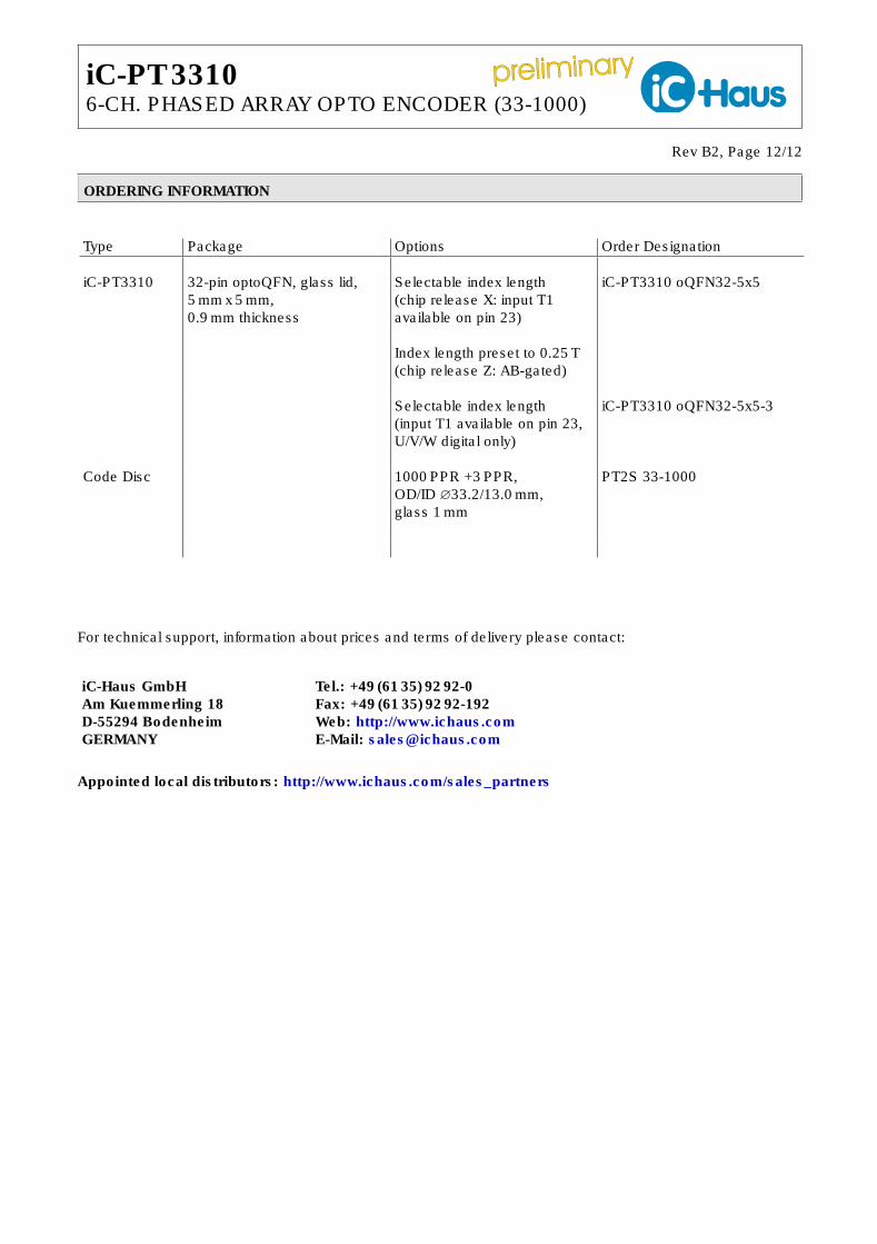
ORDERING INFORMATION
Type Package Options Order Designation
iC-PT3310 32-pin optoQFN, glass lid,
5 mm x 5 mm,
0.9 mm thickness
Selectable index length
(chip release X: input T1
available on pin 23)
Index length preset to 0.25 T
(chip release Z: AB-gated)
iC-PT3310 oQFN32-5x5
Selectable index length
(input T1 available on pin 23,
U/V/W digital only)
iC-PT3310 oQFN32-5x5-3
Code Disc 1000 PPR +3 PPR,
OD/ID ∅33.2/13.0 mm,
glass 1 mm
PT2S 33-1000
For technical support, information about prices and terms of delivery please contact:
iC-Haus GmbH Tel.: +49 (61 35) 92 92-0
Am Kuemmerling 18 Fax: +49 (61 35) 92 92-192
D-55294 Bodenheim Web: http://www.ichaus.com
GERMANY E-Mail: [email protected]
Appointed local distributors: http://www.ichaus.com/sales_partners