IC immunity modeling process validation using on-chip ...
13
HAL Id: hal-00936080 https://hal.archives-ouvertes.fr/hal-00936080 Submitted on 3 Feb 2014 HAL is a multi-disciplinary open access archive for the deposit and dissemination of sci- entific research documents, whether they are pub- lished or not. The documents may come from teaching and research institutions in France or abroad, or from public or private research centers. L’archive ouverte pluridisciplinaire HAL, est destinée au dépôt et à la diffusion de documents scientifiques de niveau recherche, publiés ou non, émanant des établissements d’enseignement et de recherche français ou étrangers, des laboratoires publics ou privés. IC immunity modeling process validation using on-chip measurements Sonia Ben Dhia, Alexandre Boyer, Bertrand Vrignon, Mikael Deobarro To cite this version: Sonia Ben Dhia, Alexandre Boyer, Bertrand Vrignon, Mikael Deobarro. IC immunity modeling process validation using on-chip measurements. Journal of Electronic Testing, Springer Verlag, 2012, 28 (3), pp.339-348. 10.1007/s10836-012-5294-3. hal-00936080
Transcript of IC immunity modeling process validation using on-chip ...

HAL Id: hal-00936080https://hal.archives-ouvertes.fr/hal-00936080
Submitted on 3 Feb 2014
HAL is a multi-disciplinary open accessarchive for the deposit and dissemination of sci-entific research documents, whether they are pub-lished or not. The documents may come fromteaching and research institutions in France orabroad, or from public or private research centers.
L’archive ouverte pluridisciplinaire HAL, estdestinée au dépôt et à la diffusion de documentsscientifiques de niveau recherche, publiés ou non,émanant des établissements d’enseignement et derecherche français ou étrangers, des laboratoirespublics ou privés.
IC immunity modeling process validation using on-chipmeasurements
Sonia Ben Dhia, Alexandre Boyer, Bertrand Vrignon, Mikael Deobarro
To cite this version:Sonia Ben Dhia, Alexandre Boyer, Bertrand Vrignon, Mikael Deobarro. IC immunity modeling processvalidation using on-chip measurements. Journal of Electronic Testing, Springer Verlag, 2012, 28 (3),pp.339-348. 10.1007/s10836-012-5294-3. hal-00936080

1
IC immunity modeling process validation using on-chip measurements
S. Ben Dhia (1)(2), A. Boyer (1)(2), B. Vrignon (3), M. Deobarro (3)
(1) CNRS ; LAAS ; 7 avenue du colonel Roche, F-31077 Toulouse Cedex 4, France
(2) Université de Toulouse ; UPS, INSA, INP, ISAE ; UT1, UTM, LAAS ; F-31077 Toulouse
Cedex 4, France
(3) Freescale Semiconductor 134 avenue du General Eisenhower, 31023 Toulouse, France
Abstract— Developing integrated circuit (IC) immunity models and simulation flow has become one of the major concerns of ICs suppliers to predict whether a chip will pass susceptibility tests before fabrication and avoid redesign cost. This paper presents an IC immunity modeling process including the standard immunity test applied to a dedicated test chip. An on-chip voltage sensor is used to characterize the radio frequency interference propagation inside the chip and thus validate the immunity modeling process.
Keywords - Integrated circuit, on-chip measurement, immunity modelling, power supply network modelling.
I. INTRODUCTION
These last years, the concerns about electromagnetic compatibility (EMC) of integrated circuits (emission and susceptibility issues) have grown considerably [1]. Susceptibility of ICs has become one of the major issues for all circuit classes (digital, analog, RF, power). Small changes in circuit or printed circuit board design may increase the susceptibility of electronic equipment by several orders of magnitude. In order to reduce IC redesign costs and time-to-market, the evaluation of non-compliance risks during design stage has become critical. IC manufacturers and customers use standardized measurement methods [2] to characterize the susceptibility of components. Designers need models and simulation tools compatible with their design flows to be able to evaluate the compliance to standard susceptibility tests prior IC fabrication.
EMC models must be able to predict accurately IC electromagnetic emission [3] and susceptibility to external interference. A significant research effort was dedicated to the prediction of power integrity and parasitic emission in large scale circuits at early design phases [4]. However simulation of susceptibility is more challenging. The definition of a standard simulation methodology or model is not obvious because susceptibility measurement requires complex set-ups. Moreover origins of disturbances are often complex and linked with non-linear effects which required confidential data to be modeled. The complexity of the injection path model, the internal circuit modeling, and time-consuming iterative simulations are major issues.
In this context, measuring the transfer function of the noise induced by electromagnetic interference (EMI) to circuit sensitive nodes is critical for IC designers for two reasons: first, it helps to understand the circuit susceptibility because both the sensitivity level to voltage fluctuations applied on its terminal and transfer function of EMI coupling path can be extracted; secondly, it helps to validate models of disturbed functions and EMI-coupling path in order to predict accurately the compliance to standard susceptibility limits.
Although numerous tools and prediction methodologies have been developed, measuring accurately on-chip noise remains necessary for designers for model validation and design optimization.
The objective of this paper is to validate, with on-chip measurements, an IC immunity modeling process in order to help standardization group to build a standard immunity model. In the following sections, the immunity modeling process is described (section II) and applied to a test vehicle to model the passive distribution network of logic cores (section III). Then, section IV is dedicated to the validation of this modeling process using IC off-chip and on-chip characterizations. In the last part (section V), based on the comparisons between simulation and experimental results, a
2
discussion is conducted on the benefits provided by on-chip measurements to help in the modeling process and fix susceptibility issues at IC level.
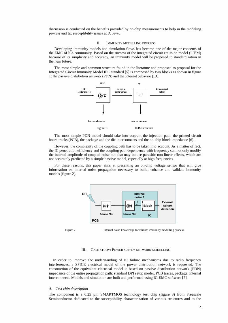
II. IMMUNITY MODELLING PROCESS
Developing immunity models and simulation flows has become one of the major concerns of the EMC of ICs community. Based on the success of the integrated circuit emission model (ICEM) because of its simplicity and accuracy, an immunity model will be proposed to standardization in the near future.
The most simple and common structure found in the literature and proposed as proposal for the Integrated Circuit Immunity Model IEC standard [5] is composed by two blocks as shown in figure 1: the passive distribution network (PDN) and the internal behavior (IB).
Figure 1. ICIM structure
The most simple PDN model should take into account the injection path, the printed circuit board tracks (PCB), the package and the die interconnects and the on-chip block impedance [6].
However, the complexity of the coupling path has to be taken into account. As a matter of fact, the IC penetration efficiency and the coupling path dependence with frequency can not only modify the internal amplitude of coupled noise but also may induce parasitic non linear effects, which are not accurately predicted by a simple passive model, especially at high frequencies.
For these reasons, this paper aims at presenting an on-chip voltage sensor that will give information on internal noise propagation necessary to build, enhance and validate immunity models (figure 2).
ICExternal PDN Internal PDN
RFI
PCB
BlockExternalfailure
detection
Internalnoise ?
Figure 2. Internal noise knowledge to validate immunity modelling process.
III. CASE STUDY: POWER SUPPLY NETWORK MODELLING
In order to improve the understanding of IC failure mechanisms due to radio frequency
interferences, a SPICE electrical model of the power distribution network is requested. The construction of the equivalent electrical model is based on passive distribution network (PDN) impedance of the entire propagation path: standard DPI setup model, PCB traces, package, internal interconnects. Models and simulation are built and performed using IC-EMC software [7].
A. Test chip description
The component is a 0.25 µm SMARTMOS technology test chip (figure 3) from Freescale Semiconductor dedicated to the susceptibility characterization of various structures and to the

3
measurements of the propagation of external radio frequency interferences along power supply rails. The test chip is packaged in 128 pins Quad Flat Package. The circuit is mounted on a specific 150×150 4 layers board (figure 4) defined by the standard IEC 62132 dedicated to susceptibility tests. Ten on-chip sensors have been implemented in the chip to monitor noise propagation on each dedicated power supply (I/O, PLL, Logic cores and regulator). The experiment presented in the following paragraph concerns the susceptibility of one of the logic cores.
LOGIC CORE (x4)
PLL
Calibration SENSORS
RegulatorsI/O
Sensors
Sen
so
rsSensors
Sen
so
rs
LOGIC CORE (x4)
PLL
Calibration SENSORS
RegulatorsI/O
Sensors
Sen
so
rsSensors
Sen
so
rs
Figure 3. Test chip dedicated to RFI measurements
Figure 4. EMC Test vehicle printed circuit board
B. Package and Internal PDN modelling(IC level)
Core supply passive models have been extracted from various methods: • netlist extraction and analytical calculation from geometrical data
• on-package impedance measurements using probes and Vector network analyser (VNA)
In order to remove spurious effects of the test board, measurements are performed directly on the package with adapted coplanar probes. Measurements are done by placing the probes on VDD and VSS pins.
Figure 5 details the encapsulated IC model. Internal supply network is modelled by on-chip pads, decoupling and core capacitances connected to interconnects resistive and inductive lumped elements. Values of on-chip capacitances have been extracted from the netlist. The on-chip capacitance is due to intrinsic parasitic capacitance of the core and added MOS capacitance. Package pins parasitic effects have been calculated from geometrical data. Moreover, as devices are designed on a low doping epitaxial layer on top of a P+ substrate and as all VSS of all the blocks of the circuit are connected to the circuit substrate, the substrate coupling has to be taken into account in the model. Substrate coupling between VSS pins is modelled by resistances extracted from DC measurements. Figure 6 presents comparison between simulation and measurement of the impedance profile between power supply and ground pins. The PDN impedance profile simulated on the package pins correlates with accuracy to external VNA measurements up to 800 MHz.

4
Figure 5. IC and package passive distribution network model (substrate coupling model is not included on the schematic)
Figure 6. Comparison between measurement and simulation of internal PDN impedance
C. External PDN Modeling (PCB level)
A PCB model including PCB tracks, power plane and external decoupling capacitances is added to the previous package and die PDN model (figure 7). The PCB track model is extracted from analytical calculation from the PCB geometrical data and composed of 2 distributed RLC cells. The external decoupling capacitance is represented by a capacitor and its parasitic inductance and resistance. Figure 8 presents the comparison between simulation and measurement of the impedance profile between power supply and ground pins. The simulation of the PDN impedance profile fits perfectly with the measurement up to 500 MHz. Above 500 MHz the effect of PCB power plane is not modeled enough accurately, but the correlation remains acceptable.
Figure 7. Passive distribution network model including PCB tracks

5
Figure 8. Comparison between impedance measurement and simulation of complete PDN (PCB,
package and die)
D. Standard DPI set-up modelling
A very popular and efficient method in order to apply a conducted disturbance to a component is the Direct Power Injection (DPI) [8]. This method consists in injecting harmonic disturbances through a small and discrete capacitor. Figure 9 describes the DPI set-up. A coaxial connector on the test board is dedicated to DPI injection, providing a 50 Ω adapted path from the output of the amplifier to the injection capacitor. The targeted frequency band is 1MHz – 1GHz, the maximum forward power is set to 45 dBm. A 6.8nF capacitor is used to superimpose a conducted disturbance to the DC supply. A choke inductance is used to protect the DC power supply from the RFI.
Pforw PreflRF source & amplifier
Coupler
Device under test
DC supply
DPI capacitance
Decoupling network
Susceptibility criterion
monitoring
Figure 9. DPI test set-up
S11 parameter measurements have been done from the input coaxial connector for RFI injection to extract a model of the complete DPI injection path. The model contains an ideal RF source which generates a sinusoidal signal, a black box directional coupler (including analytical formulas), a DPI capacitor and its parasitic inductance and resistance. The choke inductor is modeled by an inductance and some parasitic elements. The DPI setup model is added to the complete PDN model as shown figure 10.
Figure 10. Complete Passive distribution network including immunity test model
From this final model, the external RFI propagation can be simulated inside the chip. The IC
susceptibility can be correlated with internal core power supply fluctuations and external RFI.

6
IV. MODELLING PROCESS VALIDATION USING ON-CHIP MEASUREMENTS
The objective is now to validate, with on chip measurements, the IC core immunity modeling
process. In this section, the on-chip sensor used to measure internal power supply fluctuations is presented as well as the experiments.
A. Internal voltage sensor
1) Random acquisition principle
On-chip noise measurement techniques have been used for power integrity and parasitic emission characterization of digital ICs, but they have never been used for the characterization of susceptibility to EMI. The proposed sensor was firstly designed, in the early 2000 [9], to accurately measure on chip noise in time domain to address signal and power integrity issues [10].
The acquisition is based on an on-chip sample and hold circuit that directly probes the voltage within IC interconnects (figure 11). The sensor is used in a random mode acquisition [11] to handle non repeatable phenomenon, like external RFI propagated inside a chip. Each rising edge of the sampling command activates a sample and hold cell which subsamples randomly the input signal. As explained on figure 11, the acquired samples form a set of measurements of a random variable. Determining the probability distribution of the measured signal and extracting its statistical characteristics, such as mean, peak-to-peak amplitude, standard deviation…, provides valuable information. A histogram is an adapted graphical representation of a probability distribution.
The probability density of a signal can be only calculated if the number of sampled points is high enough and the measured interference and the sampling command frequencies are not multiples [12].
Sampling commandSampling cell
Signal to measure
+
_
FollowingAOP
SampleddataProbe
Figure 11. Sensor architecture and Random acquisition technique
The acquisition accuracy depends on both the number of samples and the number of bins (i.e. a
discrete interval of the measured signal range) which has to be carefully chosen. A small number of bins reduces the resolution of the histogram and degrades the accuracy of the extraction of statistical properties, while a too large number of bins increases the number of spikes on the histogram. Several theoretical works have attempted to provide algorithms [13] or formulas to find an optimal number of bins N from the number of samples n, such as Sicard-Max or Sturge formula (1)[12]. A usual choice of bin number is given by the square root choice given by (2).

7
( ) )(log.3.31log1 102 nnN +=+= (1)
nN = (2) However, all of these formulas suffer from the assumption made on the type of distribution and
the large number of samples. Therefore, the number of bins can be experimentally set to optimize the number of samples and the histogram resolution. A rule of thumb is to ensure that the bin width remains larger than the measurement resolution. Experimental results have shown that the sensor resolution is about 10 mV.
In order to verify the correctness of probability distribution extracted from sensor measurement,
the PDF (Probability Density Function) of a basic signal is measured with the on-chip sensor. Fig. 12 presents the histogram obtained with a sinusoidal signal. The signal frequency is set to 10 MHz, its peak-to-peak amplitude is equal to 3 V. The signal is randomly sampled 2000 times at 50 kHz. The number of bins is set to 100, the bin width is equal to 37.5 mV. As shown on Fig. 12, the sensor measurement result is in accordance with the theoretical probability density function given by (3).
( ) 1,1
12
<−
= xx
xpπ (3)
Figure 12. Measured and theoretical probability density function of a sinusoidal signal
This random mode is not able to characterize signal frequency contents or transient characteristics. The probability density, extracted from measurement data, gives very valuable information to designers:
• the amplitude of the signal provides a quantification of the circuit robustness to voltage fluctuations
• the distribution of the signal provides indirect information about the shape of the signal and distortion (e.g. due to clamp devices).
This acquisition mode can provide valuable information about circuit susceptibility. First, for a given type of disturbance, the average amplitude of the EMI-induced noise can be extracted from the signal amplitude PDF. Moreover, for large amplitude disturbance injection, changes in amplitude PDF shape suggest that some distortions induced by the circuit (e.g. ESD clamp devices triggered by large disturbances) affect the measured signal.
2) On chip sensor architecture
The sensor is made of three main elements: an attenuator, a sample and hold cell which operates in sub sampling mode and an output amplifier. The attenuator and the S/H cell form a high impedance probe which ensures a low intrusive voltage measurement.
To isolate the sensor to external disturbances and to noise produced by the other blocks, the output amplifier and sensor input-outputs are supplied by an external and dedicated 5 V power supply. At board level, this power supply is separated and carefully decoupled. The S/H cell and

8
the amplifier input stage are supplied by a quiet 2.5 V power supply provided by an internal built-in voltage regulator and powered by the 5 V sensor power supply. To prevent from interference coupling on the sensor by the substrate, all the devices of the sensor are isolated from the P substrate by a buried N layer and dielectric-filled trenches on the sides.
The attenuator and the S/H cell (fig.13) are the most critical part of the sensor to ensure a large bandwidth, improve the linearity and reduce the voltage dependence. They are made of isolated low voltage transistors to prevent the impact of external disturbance and reach a large bandwidth.
The S/H cell is composed of a transmission gate switch and a storage node composed of parasitic capacitors of the switch, input capacitor of the amplifier and the storage capacitor. The sizes of the transmission gate transistors are carefully chosen to optimize the bandwidth and reduce the voltage dependence of the on-state resistance. However, when the S/H cell turns off, a charge injection in the parasitic capacitances between the control signal and the storage node arises. A parasitic offset can be induced on the output voltage. Despite a reduction of the bandwidth, this effect can be reduced by increasing the storage capacitor. Moreover, adding a dummy transmission gate can help to compensate the charge injection effect.
An analog output signal is driven off the chip, externally stored and processed by a digital acquisition card. The output amplifier is a non-inverting CMOS amplifier with a gain of 2, made of a 2.5 V rail-to-rail input stage and a 5 V AB class output stage. The output stage has been optimized to keep a constant gain up to 2.5 MHz, reduce parasitic offset and stability issues. The bandwidth of the output amplifier does not affect the sensor bandwidth since the amplifier does not process the sensor input signal, but the S/H output signal. However, the sampling frequency has to be smaller than the amplifier cut-off frequency to prevent the filtering of the sampling signal, which can affect the measured PDF.
A complete characterization of the sensor performances (offset, bandwidth, sensitivity to
temperature) has been conducted to calibrate the sensor, and compensate its nonideal behavior. For this purpose, a calibration sensor has been implemented. Its probe is connected to a
dedicated input pad. For different input voltage values included in the sensor input voltage range, the input signal is
sampled ten times at various moments, and the standard deviation of the input sample distribution is computed. The measurement repeatability is estimated to be ±4 mV.
The bandwidth of the sensor is the frequency range over which the PDF of an input signal can be correctly extracted. It has been measured from the calibration sensor by sampling a sinusoidal signal of known amplitude with a varying frequency. The signal is sampled randomly, and the amplitude of the signal is deduced from its PDF. The gain of the sensor is nearly constant up to 2.5 GHz.
Figure 13. Schematic of the attenuator and the sample and hold cell

9
B. Characterization of propagation of conducted noise along a power supply rail
The on-chip sensor has been implemented on the power supply rail of the digital core. The sensor aims at measuring the amplitude and the statistical distribution of voltage fluctuations induced by conducted EMI. A DPI test bench is used to inject harmonic disturbances on the power supply pin of the component. Figure 14 details the experiment. Power supply voltage fluctuations are measured either externally with an oscilloscope active probe, or internally with the sensor. The oscilloscope and the active probe present large frequency bandwidths (2.5 GHz) to characterize accurately EMI voltage fluctuations up to 1 GHz. Sensor output samples are acquired thanks to an acquisition card. A post-processing tool extracts the amplitude of the voltage fluctuation.
DPI Capacitor
Decoupling network
Chip under test
P INC P refl
Directional coupler
Signal Synthesizer
Amplifier
Power meter
sensor
Oscilloscope
RFI
(off-chip meas .)
DPI Capacitor
Decoupling network
Chip under test
P INC P refl
Directional coupler
Signal Synthesizer
Amplifier
Power meter
sensor
Oscilloscope
RFI
(off-chip meas .)
Logic core
Figure 14. Experimental set-up
In this experiment, EMI level required to induce a given power supply voltage fluctuation on-
chip and off-chip is measured. The amplitude criterion on power supply fluctuation is fixed to +/- 10 % of the nominal power supply voltage..
Results illustrated in Figure 15 show the susceptibility threshold of the digital core with the 0.25 V voltage fluctuation criterion applied on the power supply net, obtained with on-chip and off-chip measurements. An over-estimated immunity level with the off-chip measurement is observed. When the EMI frequency is less than 50 MHz, both measurement methods provides the same susceptibility thresholds, i.e for a given EMI amplitude, the power supply voltage fluctuation is the same off-chip and on-chip. However, above 50 MHz, on-chip and off-chip measurement methods give divergent results. The difference between both susceptibility thresholds reaches 13 dB. The off-chip measurements indicate that the EMI coupling across the power supply pin is increasing between 100 and 400 MHz, inducing a higher susceptibility. Then, it remains quite stable up to 1 GHz despite several resonances associated to PCB power planes. On the contrary, the on-chip sensor measurements show that the internal EMI coupling along the digital core power supply rails is optimized at 150 MHz and tends to decrease up to 400 MHz, increasing the immunity. This result shows that on-chip and off-chip measurements can lead to significant differences in the evaluation of the susceptibility of the digital core. As the cut-off frequencies of both measurement systems exceed 1 GHz, the observed differences cannot be explained by their frequency limits. The origin of these differences is linked to the different measurement locations. Package and circuit filtering affect differently on-chip and off-chip EMI-induced noise. The significant measurement discrepancies between on-chip and off-chip EMI-induced noise can lead to different evaluation of circuit susceptibility. This measurement shows that the on-chip noise sensor provides a more accurate measurement of EMI-coupling across the digital core above 50 MHz. Around 100 MHz, the amount of EMI-induced noise tends to be underestimated by off-chip measurement, while it is overestimated above 200 MHz. On-chip characterization of the power supply fluctuation amplitude is then necessary to understand and predict internal blocks failures. Moreover, the complex on-chip propagation of conducted EMI can be understood more clearly by on-chip noise sensor measurement.

10
Figure 15. Comparison of the susceptibility threshold between on-chip and off-chip measurements .
V. MODELLING PROCESS VALIDATION
In order to validate the proposed IC immunity modelling process, on-chip and off-chip EMI coupling measurements are compared to the ones predicted by simulation from the model shown in figure 10. The following figures show the comparisons between measured and simulated susceptibility level to induce +/- 0.25 V power supply voltage fluctuations off-chip (fig. 16) and on-chip (fig. 17).
Differences between measurements and simulations are mainly due to measurement errors, inaccuracies of external passive devices (e.g. quality factor of decoupling capacitors, parasitic parallel capacitor of choke inductances), package inductances and substrate coupling models. However, simulation curves fits enough with on-chip measurement curves to validate the proposed model. The PDN model allows an accurate prediction of the noise coupled on the power supply of the digital core. Connecting this PDN model to an accurate IB model will provide a reliable prediction of susceptibility level for core functional failures.
Figure 16. Comparison between measurement and simulation of the external EMI coupling
Figure 17. Comparison between measurement and simulation of the on-chip EMI coupling
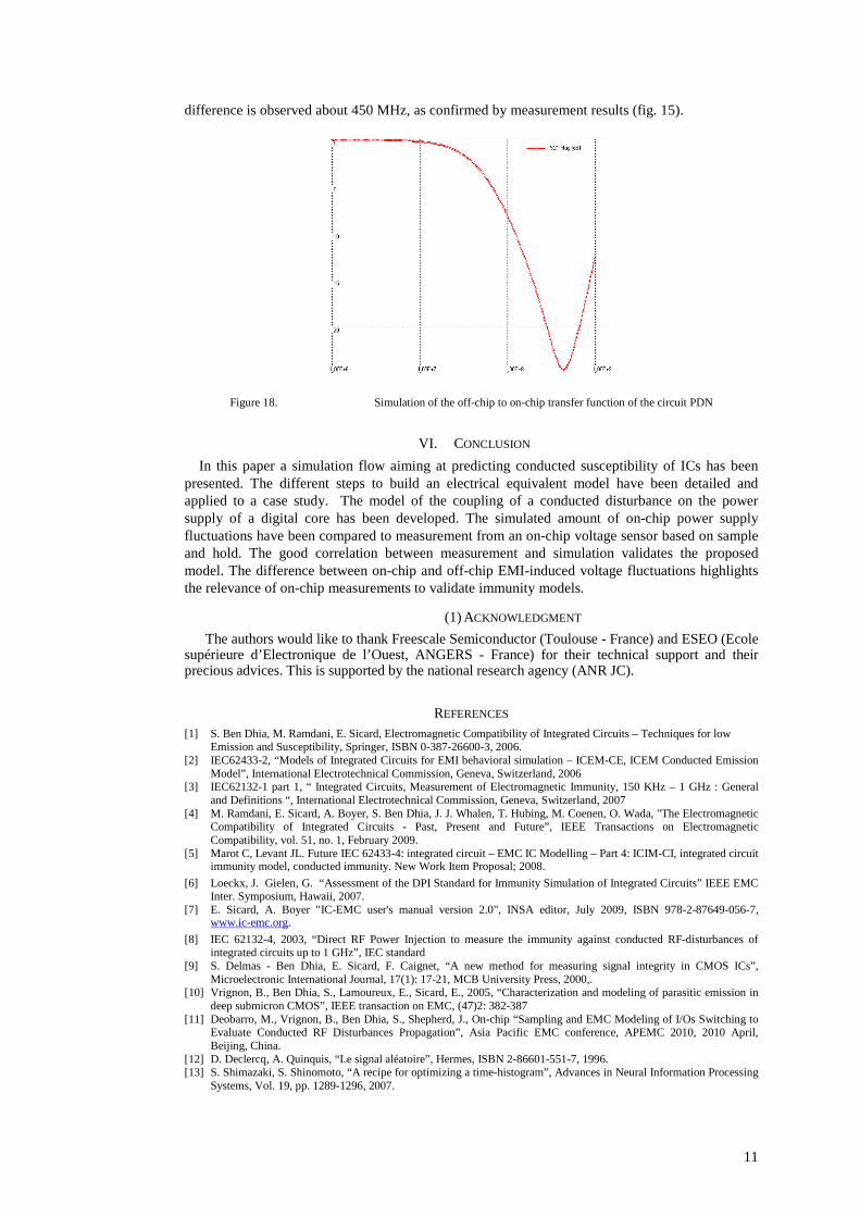
Finally, the developed PDN model is used to compute the transfer function between the power
supply package pin and on-chip digital core power supply. Figure 18 presents the simulation of the off-chip to on-chip transfer function of the circuit PDN, given in term of S21 parameter. Below 50 MHz, the transfer function is higher than -3 dB so that the off-chip and on-chip power supply voltage fluctuations are similar. However, they tend to be different above 50 MHz. The larger
11
difference is observed about 450 MHz, as confirmed by measurement results (fig. 15).
Figure 18. Simulation of the off-chip to on-chip transfer function of the circuit PDN
VI. CONCLUSION
In this paper a simulation flow aiming at predicting conducted susceptibility of ICs has been presented. The different steps to build an electrical equivalent model have been detailed and applied to a case study. The model of the coupling of a conducted disturbance on the power supply of a digital core has been developed. The simulated amount of on-chip power supply fluctuations have been compared to measurement from an on-chip voltage sensor based on sample and hold. The good correlation between measurement and simulation validates the proposed model. The difference between on-chip and off-chip EMI-induced voltage fluctuations highlights the relevance of on-chip measurements to validate immunity models.
(1) ACKNOWLEDGMENT
The authors would like to thank Freescale Semiconductor (Toulouse - France) and ESEO (Ecole supérieure d’Electronique de l’Ouest, ANGERS - France) for their technical support and their precious advices. This is supported by the national research agency (ANR JC).
REFERENCES [1] S. Ben Dhia, M. Ramdani, E. Sicard, Electromagnetic Compatibility of Integrated Circuits – Techniques for low
Emission and Susceptibility, Springer, ISBN 0-387-26600-3, 2006. [2] IEC62433-2, “Models of Integrated Circuits for EMI behavioral simulation – ICEM-CE, ICEM Conducted Emission
Model”, International Electrotechnical Commission, Geneva, Switzerland, 2006 [3] IEC62132-1 part 1, “ Integrated Circuits, Measurement of Electromagnetic Immunity, 150 KHz – 1 GHz : General
and Definitions “, International Electrotechnical Commission, Geneva, Switzerland, 2007 [4] M. Ramdani, E. Sicard, A. Boyer, S. Ben Dhia, J. J. Whalen, T. Hubing, M. Coenen, O. Wada, "The Electromagnetic
Compatibility of Integrated Circuits - Past, Present and Future”, IEEE Transactions on Electromagnetic Compatibility, vol. 51, no. 1, February 2009.
[5] Marot C, Levant JL. Future IEC 62433-4: integrated circuit – EMC IC Modelling – Part 4: ICIM-CI, integrated circuit immunity model, conducted immunity. New Work Item Proposal; 2008.
[6] Loeckx, J. Gielen, G. “Assessment of the DPI Standard for Immunity Simulation of Integrated Circuits” IEEE EMC Inter. Symposium, Hawaii, 2007.
[7] E. Sicard, A. Boyer "IC-EMC user's manual version 2.0", INSA editor, July 2009, ISBN 978-2-87649-056-7, www.ic-emc.org.
[8] IEC 62132-4, 2003, “Direct RF Power Injection to measure the immunity against conducted RF-disturbances of integrated circuits up to 1 GHz”, IEC standard
[9] S. Delmas - Ben Dhia, E. Sicard, F. Caignet, “A new method for measuring signal integrity in CMOS ICs”, Microelectronic International Journal, 17(1): 17-21, MCB University Press, 2000,.
[10] Vrignon, B., Ben Dhia, S., Lamoureux, E., Sicard, E., 2005, “Characterization and modeling of parasitic emission in deep submicron CMOS”, IEEE transaction on EMC, (47)2: 382-387
[11] Deobarro, M., Vrignon, B., Ben Dhia, S., Shepherd, J., On-chip “Sampling and EMC Modeling of I/Os Switching to Evaluate Conducted RF Disturbances Propagation”, Asia Pacific EMC conference, APEMC 2010, 2010 April, Beijing, China.
[12] D. Declercq, A. Quinquis, “Le signal aléatoire”, Hermes, ISBN 2-86601-551-7, 1996. [13] S. Shimazaki, S. Shinomoto, “A recipe for optimizing a time-histogram”, Advances in Neural Information Processing
Systems, Vol. 19, pp. 1289-1296, 2007.

12