IBM Research Reportdomino.watson.ibm.com/library/CyberDig.nsf/papers/... · MAGNETIC TUNNEL...
17
RC23525 (W0502-076) February 14, 2005 Materials Science IBM Research Report Magnetic Tunnel Junction-Based MRAM and Related Processing Issues E. J. O'Sullivan IBM Research Division Thomas J. Watson Research Center P.O. Box 218 Yorktown Heights, NY 10598 Research Division Almaden - Austin - Beijing - Haifa - India - T. J. Watson - Tokyo - Zurich LIMITED DISTRIBUTION NOTICE: This report has been submitted for publication outside of IBM and will probably be copyrighted if accepted for publication. It has been issued as a Research Report for early dissemination of its contents. In view of the transfer of copyright to the outside publisher, its distribution outside of IBM prior to publication should be limited to peer communications and specific requests. After outside publication, requests should be filled only by reprints or legally obtained copies of the article (e.g. , payment of royalties). Copies may be requested from IBM T. J. Watson Research Center , P. O. Box 218, Yorktown Heights, NY 10598 USA (email: [email protected]). Some reports are available on the internet at http://domino.watson.ibm.com/library/CyberDig.nsf/home .
Transcript of IBM Research Reportdomino.watson.ibm.com/library/CyberDig.nsf/papers/... · MAGNETIC TUNNEL...
RC23525 (W0502-076) February 14, 2005Materials Science
IBM Research Report
Magnetic Tunnel Junction-Based MRAM and Related Processing Issues
E. J. O'SullivanIBM Research Division
Thomas J. Watson Research CenterP.O. Box 218
Yorktown Heights, NY 10598
Research DivisionAlmaden - Austin - Beijing - Haifa - India - T. J. Watson - Tokyo - Zurich
LIMITED DISTRIBUTION NOTICE: This report has been submitted for publication outside of IBM and will probably be copyrighted if accepted for publication. It has been issued as a ResearchReport for early dissemination of its contents. In view of the transfer of copyright to the outside publisher, its distribution outside of IBM prior to publication should be limited to peer communications and specificrequests. After outside publication, requests should be filled only by reprints or legally obtained copies of the article (e.g. , payment of royalties). Copies may be requested from IBM T. J. Watson Research Center , P.O. Box 218, Yorktown Heights, NY 10598 USA (email: [email protected]). Some reports are available on the internet at http://domino.watson.ibm.com/library/CyberDig.nsf/home .
MAGNETIC TUNNEL JUNCTION-BASED MRAM AND RELATED PROCESSING ISSUES
E. J. O’Sullivan IBM Research Division
Thomas J. Watson Research Center P.O. Box 218
Yorktown Hts., NY 10598, USA
ABSTRACT
Magnetic tunnel junction (MTJ) research and development aimed at developing fast,
nonvolatile MRAM memory continues to grow at a rapid pace. The subject of the first part of this paper is memory applications of MTJs, and includes an introduction to them, details of the stack layers, prospects for achieving higher tunneling magnetoresistance (TMR), data writing methods, and demonstrator chips. Several important aspects of fabricating MTJs, including needed future processing enhancements, are discussed in the second part: stack deposition, MTJ patterning (including etching and free layer conversion methods), wet cleaning, and thermal stability.
INTRODUCTION
Interest in spin-electronics has surged over the past 6 - 8 years. Magnetic tunnel
junctions (1), which are based on magnetic hysteresis for data storage, are an important subset of this field. An MTJ-based MRAM would possess several important features: nonvolatility (similar to “flash” memory, but MRAM has much higher data writing endurance), which means virtually “instant-on” computers; fast writing speeds (2-4 ns) similar to static random access memory (SRAM); it may approach dynamic random access memory (DRAM) density (subject to solving scaling issues). Thus, MRAM has the potential for being a universal memory solution; it seems to be initially attractive for mobile applications and for use as embedded memory in standard logic.
This paper is in two parts. Following an introduction to MTJs, the first part discusses
the evolution of tunneling magnetoresistance (TMR, although it is often simply referred to as MR) over the past decade, data writing methods, and demonstrator chips. The second part deals with important fabrication challenges, some of which arise from introducing a magnetic memory technology into a microelectronics back-end-of-line (BEOL) fabrication environment, e.g. MTJ stack patterning, and thermal stability.
MAGNETIC TUNNEL JUNCTION-BASED MRAM
In a typical MTJ stack (Fig. 1), an antiferromagnetic (AF) layer, e.g. a Pt-Mn alloy,
is located above the bottom electrode. The Pt-Mn pins the lower ferromagnetic (FM) layer of an antiparallel (AP), Ru-coupled FM sandwich. A thin (10 – 20 Ǻ) AlOx barrier
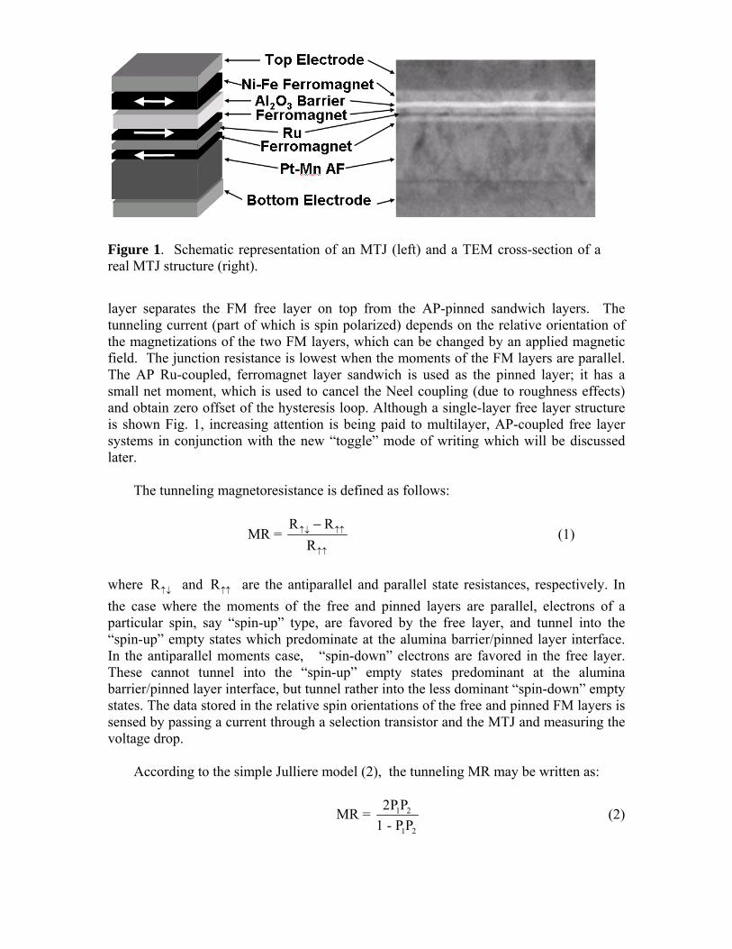
Figure 1. Schematic representation of an MTJ (left) and a TEM cross-section of a real MTJ structure (right).
layer separates the FM free layer on top from the AP-pinned sandwich layers. The tunneling current (part of which is spin polarized) depends on the relative orientation of the magnetizations of the two FM layers, which can be changed by an applied magnetic field. The junction resistance is lowest when the moments of the FM layers are parallel. The AP Ru-coupled, ferromagnet layer sandwich is used as the pinned layer; it has a small net moment, which is used to cancel the Neel coupling (due to roughness effects) and obtain zero offset of the hysteresis loop. Although a single-layer free layer structure is shown Fig. 1, increasing attention is being paid to multilayer, AP-coupled free layer systems in conjunction with the new “toggle” mode of writing which will be discussed later. The tunneling magnetoresistance is defined as follows:
R R
MR = R
↑↓ ↑
↑↑
↑− (1)
where and are the antiparallel and parallel state resistances, respectively. In the case where the moments of the free and pinned layers are parallel, electrons of a particular spin, say “spin-up” type, are favored by the free layer, and tunnel into the “spin-up” empty states which predominate at the alumina barrier/pinned layer interface. In the antiparallel moments case, “spin-down” electrons are favored in the free layer. These cannot tunnel into the “spin-up” empty states predominant at the alumina barrier/pinned layer interface, but tunnel rather into the less dominant “spin-down” empty states. The data stored in the relative spin orientations of the free and pinned FM layers is sensed by passing a current through a selection transistor and the MTJ and measuring the voltage drop.
R↑↓ R↑↑
According to the simple Julliere model (2), the tunneling MR may be written as:
1 2
1 2
2P PMR = 1 - P P
(2)
where P1 and P2 are the electron spin polarizations at the FM/tunnel barrier interfaces. Typically the magnitude of the resistance difference between both states is ca. 30 – 50 %, which appears to be large enough for practical application (integration with CMOS technology). For an MTJ with a 50 % MR ratio and similar free and pinned layer/tunnel barrier interfaces, the spin polarization of the tunneling current electrons is estimated to be around 45 %.
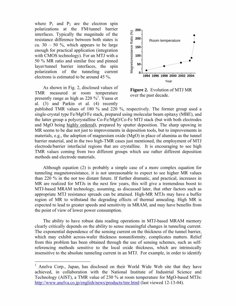
As shown in Fig. 2, disclosed values of TMR measured at room temperature presently range as high as 220 %1. Yuasa et al. (3) and Parkin et al. (4) recently published TMR values of 180 % and 220 %, respectively. The former group used a single-crystal type Fe/MgO/Fe stack, prepared using molecular beam epitaxy (MBE), and the latter group a polycrystalline Co-Fe/MgO/Co-Fe MTJ stack (but with both electrodes and MgO being highly ordered), prepared by sputter deposition. The sharp upswing in MR seems to be due not just to improvements in deposition tools, but to improvements in materials, e.g., the adoption of magnesium oxide (MgO) in place of alumina as the tunnel barrier material, and in the two high-TMR cases just mentioned, the employment of MTJ electrode/barrier interfacial regions that are crystalline. It is encouraging to see high TMR values coming from two different groups which use rather different deposition methods and electrode materials.
1994 1996 1998 2000 2002 20040
50
100
150
200
250
Mag
Year
neto
resi
stan
ce R
atio
(%)
Room temperature
Figure 2. Evolution of MTJ MR over the past decade.
Although equation (2) is probably a simple case of a more complex equation for
tunneling magnetoresistance, it is not unreasonable to expect to see higher MR values than 220 % in the not too distant future. If further dramatic, and practical, increases in MR are realized for MTJs in the next few years, this will give a tremendous boost to MTJ-based MRAM technology, assuming, as discussed later, that other factors such as appropriate MTJ resistance spreads can be attained. High-MR MTJs may have a buffer region of MR to withstand the degrading effects of thermal annealing. High MR is expected to lead to greater speeds and sensitivity in MRAM, and may have benefits from the point of view of lower power consumption. The ability to have robust data reading operations in MTJ-based MRAM memory clearly critically depends on the ability to sense meaningful changes in tunneling current. The exponential dependence of the sensing current on the thickness of the tunnel barrier, which may exhibit across-wafer thickness nonuniformity, complicates matters. Relief from this problem has been obtained through the use of sensing schemes, such as self-referencing methods sensitive to the local oxide thickness, which are intrinsically insensitive to the absolute tunneling current in an MTJ. For example, in order to identify
1 Anelva Corp., Japan, has disclosed on their World Wide Web site that they have achieved, in collaboration with the National Institute of Industrial Science and Technology (AIST), a TMR value of 230 % at room temperature for MgO-based MTJs: http://www.anelva.co.jp/english/news/products/tmr.html (last viewed 12-13-04).
the memory state, a current is passed through the MTJ cell and the resulting voltage is sensed and compared to that of a reference cell (whose resistance is maintained at a fixed value) somewhere in the array.
In general, tight control of resistance spreads in arrays is a major fabrication goal in MTJ-based MRAM; overlap of the tails of the resistance distribution curves for the high resistance and low resistance states of the MTJ arrays has to be avoided. It is easily shown that unreadable bits statistically five standard deviations (or sigmas) from the mean will lead to about 2 worthless bits in 4 Mbits of memory, indicating that bits should ideally be readable about six standard deviations from the mean.
Until recently, a “half-select”
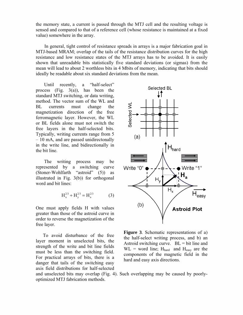
process (Fig. 3(a)), has been the standard MTJ switching, or data writing, method. The vector sum of the WL and BL currents must change the magnetization direction of the free ferromagnetic layer. However, the WL or BL fields alone must not switch the free layers in the half-selected bits. Typically, writing currents range from 5 – 10 mA, and are passed unidirectonally in the write line, and bidirectionally in the bit line.
The writing process may be
represented by a switching curve (Stoner-Wohlfarth “astroid” (5)) as illustrated in Fig. 3(b)) for orthogonal word and bit lines:
2/3 2/3 2/3x y aH H H+ = (3)
One must apply fields H with values greater than those of the astroid curve in order to reverse the magnetization of the free layer.
To avoid disturbance of the free layer moment in unselected bits, the strength of the write and bit line fields must be less than the switching field. For practical arrays of bits, there is a danger that tails of the switching easy axis field distributions for half-selected and unselected bits may overlap (Fig. 4). Such overlapping may be caused by poorly-optimized MTJ fabrication methods.
Figure 3. Schematic representations of a) the half-select writing process, and b) an Astroid switching curve. BL = bit line and WL = word line; Hhard and Heasy are the components of the magnetic field in the hard and easy axis directions.
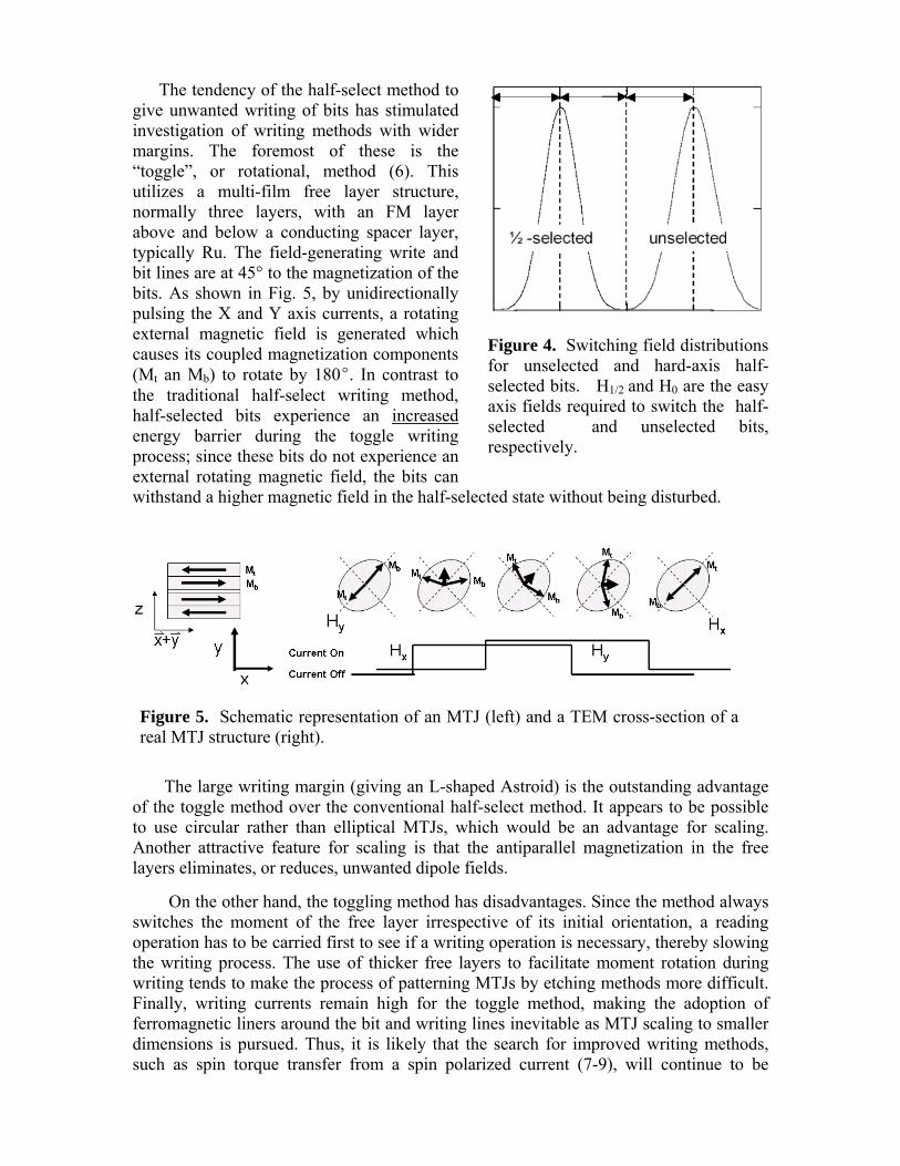
The tendency of the half-select method to give unwanted writing of bits has stimulated investigation of writing methods with wider margins. The foremost of these is the “toggle”, or rotational, method (6). This utilizes a multi-film free layer structure, normally three layers, with an FM layer above and below a conducting spacer layer, typically Ru. The field-generating write and bit lines are at 45° to the magnetization of the bits. As shown in Fig. 5, by unidirectionally pulsing the X and Y axis currents, a rotating external magnetic field is generated which causes its coupled magnetization components (Mt an Mb) to rotate by 180E. In contrast to the traditional half-select writing method, half-selected bits experience an increased energy barrier during the toggle writing process; since these bits do not experience an external rotating magnetic field, the bits can withstand a higher magnetic field in the half-selected state without being disturbed.
Figure 4. Switching field distributions for unselected and hard-axis half-selected bits. H1/2 and H0 are the easy axis fields required to switch the half-selected and unselected bits, respectively.
The large writing margin (giving an L-shaped Astroid) is the outstanding advantage of the toggle method over the conventional half-select method. It appears to be possible to use circular rather than elliptical MTJs, which would be an advantage for scaling. Another attractive feature for scaling is that the antiparallel magnetization in the free layers eliminates, or reduces, unwanted dipole fields.
Figure 5. Schematic representation of an MTJ (left) and a TEM cross-section of a real MTJ structure (right).
On the other hand, the toggling method has disadvantages. Since the method always
switches the moment of the free layer irrespective of its initial orientation, a reading operation has to be carried first to see if a writing operation is necessary, thereby slowing the writing process. The use of thicker free layers to facilitate moment rotation during writing tends to make the process of patterning MTJs by etching methods more difficult. Finally, writing currents remain high for the toggle method, making the adoption of ferromagnetic liners around the bit and writing lines inevitable as MTJ scaling to smaller dimensions is pursued. Thus, it is likely that the search for improved writing methods, such as spin torque transfer from a spin polarized current (7-9), will continue to be
vigorously pursued.
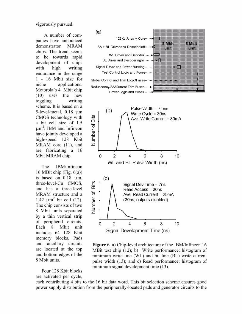
A number of com-panies have announced demonstrator MRAM chips. The trend seems to be towards rapid development of chips with high writing endurance in the range 1 - 16 Mbit size for niche applications. Motorola’s 4 Mbit chip (10) uses the new toggling writing scheme. It is based on a 5-level-metal, 0.18 µm CMOS technology with a bit cell size of 1.5 µm2. IBM and Infineon have jointly developed a high-speed 128 Kbit MRAM core (11), and are fabricating a 16 Mbit MRAM chip. The IBM/Infineon 16 MBit chip (Fig. 6(a)) is based on 0.18 µm, three-level-Cu CMOS, and has a three-level MRAM structure and a 1.42 µm2 bit cell (12). The chip consists of two 8 Mbit units separated by a thin vertical strip of peripheral circuits. Each 8 Mbit unit includes 64 128 Kbit memory blocks. Pads and ancillary circuits are located at the top and bottom edges of the 8 Mbit units. Four 128 Kbit blocks are activated per cycle, each contributing 4 bits to the 16 bit data word. This bit selection scheme ensures good power supply distribution from the peripherally-located pads and generator circuits to the
Figure 6. a) Chip-level architecture of the IBM/Infineon 16 MBit test chip (12); b) Write performance: histogram of minimum write line (WL) and bit line (BL) write current pulse width (13); and c) Read performance: histogram of minimum signal development time (13).
active portion of the memory core, particularly during the writing cycle, which includes a brief, high-peak current pulse. In each 128 Kbit block, a single WL is selected per cycle along with four equally-spaced BLs. In order to minimize magnetic interference during the writing cycle, the selected BLs are separated. A number of novel circuit features involved in the 16 Mbit design are discussed elsewhere (12). Figure 6(b) shows a histogram of the minimum BL and WL current pulse width required for a successful data writing operation (13). The BL and WL write current pulse width affects both write performance and the power used in the process. Most bits were successfully switched with a pulse width of less than 5 ns. The pulse width of 7.5 ns, in which all bits were written, corresponds to an overall write cycle time of 30 ns. Figure 6(c) shows a histogram of the minimum signal development time required for a successful data reading operation (13). Most bits were successfully read with a signal development time of less than 5 ns. The maximum signal development time of 7 ns corresponds to a read access time of 30 ns, and an average read current of 25 mA for the chip at a 30 ns cycle time. MTJ PROCESSING ISSUES
In the past few years, the impressive gains made in MTJ performance, particularly in
TMR, have been in large part fueled by materials research. The fabrication of durable, high-yield MTJ arrays, which include the advances in materials, poses major processing challenges, however. After addressing the issue of potential ferromagnetic material cross-contamination of non-MRAM technology wafers, comes the task of integrating MRAM processing into a line that is typically optimized for Cu BEOL with respect to, e.g., etching tools, and dielectrics (which are often deposited at temperatures approaching 400 °C).
The challenges of fabrication may be glimpsed using, for illustration purposes, an
SEM cross-section of the IBM/Infineon 16 Mbit demonstrator chip shown in Fig. 7. Critical areas include a) the processes associated with fabrication of the VA level, whose thin interlayer dielectric (ILD) (~ 100 nm thick) separates the MTJ from the WL; b) hardmask (HM) and MTJ etching processes; c) completely etching the MA level, yet not etching down to Cu; d) post-etch cleaning, e.g., to minimize corrosion; and e) use of stable low-temperature encapsulating dielectrics in the presence of the MTJ stack to minimize thermal degradation. Finally, a key challenge is seamless integration of the various fabrication processes. Stack Deposition Following preparation of a smooth VA-level ILD surface (a few Ǻ RMS of roughness) by chemical mechanical planarization (CMP), the MTJ stack films are usually deposited using either PVD or IBD methods. The deposition of smooth magnetic layers is critical to minimize Neel coupling effects; here is where advances in tooling play a critical role as well as in obtaining excellent across-wafer film thickness and composition
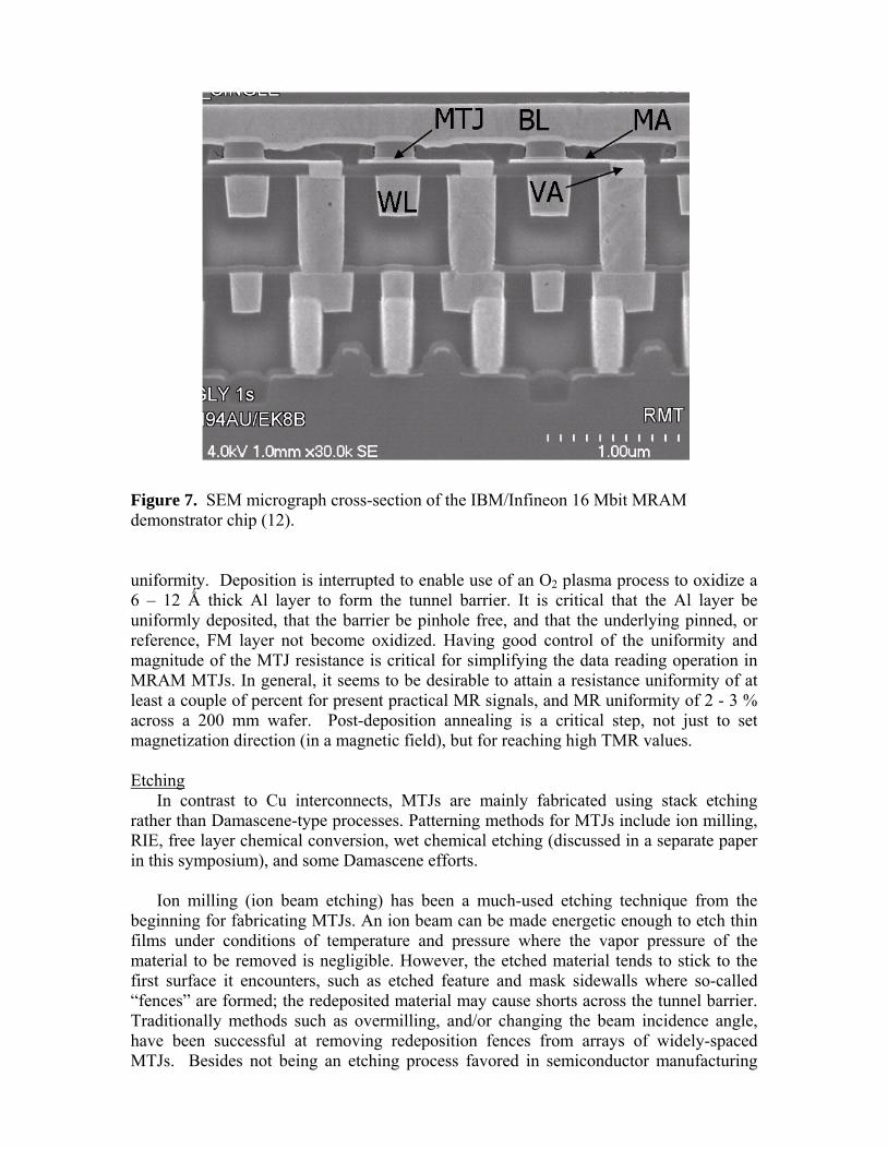
Figure 7. SEM micrograph cross-section of the IBM/Infineon 16 Mbit MRAM demonstrator chip (12). uniformity. Deposition is interrupted to enable use of an O2 plasma process to oxidize a 6 – 12 Ǻ thick Al layer to form the tunnel barrier. It is critical that the Al layer be uniformly deposited, that the barrier be pinhole free, and that the underlying pinned, or reference, FM layer not become oxidized. Having good control of the uniformity and magnitude of the MTJ resistance is critical for simplifying the data reading operation in MRAM MTJs. In general, it seems to be desirable to attain a resistance uniformity of at least a couple of percent for present practical MR signals, and MR uniformity of 2 - 3 % across a 200 mm wafer. Post-deposition annealing is a critical step, not just to set magnetization direction (in a magnetic field), but for reaching high TMR values. Etching In contrast to Cu interconnects, MTJs are mainly fabricated using stack etching rather than Damascene-type processes. Patterning methods for MTJs include ion milling, RIE, free layer chemical conversion, wet chemical etching (discussed in a separate paper in this symposium), and some Damascene efforts.
Ion milling (ion beam etching) has been a much-used etching technique from the beginning for fabricating MTJs. An ion beam can be made energetic enough to etch thin films under conditions of temperature and pressure where the vapor pressure of the material to be removed is negligible. However, the etched material tends to stick to the first surface it encounters, such as etched feature and mask sidewalls where so-called “fences” are formed; the redeposited material may cause shorts across the tunnel barrier. Traditionally methods such as overmilling, and/or changing the beam incidence angle, have been successful at removing redeposition fences from arrays of widely-spaced MTJs. Besides not being an etching process favored in semiconductor manufacturing
plants, it is not clear that ion milling can cleanly pattern dense arrays of MTJs in a high-wafer-throughput environment. Nevertheless, until another MTJ patterning method proves to be successful and widely available, ion milling should continue to play a role in patterning MTJs.
There has been recognition in the MRAM field that developing a RIE-based etching
process is strategically important for integrating MRAM with microelectronic fabrication. However, despite the tremendous success of RIE in microelectronics, when it comes to MTJ etching, it has problems due to the nonvolatility at practical processing temperatures (# 200EC) of the ferromagnetic metal etch products.
The relatively non-selective, halogen-gas-based RIE processes have received
attention in MRAM materials etching; in the 1990s the University of Florida group (14-16) and Hsiao (17) described the use of several types of RIE processes for etching ferromagnetic materials. There seems to be some chemical enhancement in plasma etching ferromagnetic layers (Ni-Fe, Ni-Fe-Co) using Cl2 (and I2 (14)) gases, with ion-assisted desorption of the halogenated, or partially halogenated, etch products overcoming their low volatilities, but with the low etch yield emphasizing the need for high-density plasma conditions to achieve practical etch rates. Despite their potential for formation of volatile ferromagnetic carbonyl etch products, especially in the case of nickel, CO-NH3 based etches (18) are largely physical in nature, and tend to be limited by low etch rates. The Anelva corporation, whose deposition tools have played a major role in the development of high-MR MTJ stacks, reported that they used a methanol (CH3OH) -containing plasma to etch the stack that, in 2003, gave the then record 70.8% MR (19).
While little information has been
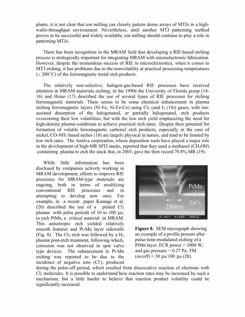
disclosed by companies actively working in MRAM development, efforts to improve RIE processes for MRAM-type materials are ongoing, both in terms of modifying conventional RIE processes and in attempting to develop new ones. For example, in a recent paper Kumagi et al. (20) described the use of a pulsed Cl2 plasma with pulse periods of 10 to 100 µs, to etch PtMn, a critical material in MRAM. This anisotropic etch yielded relatively smooth features and Pt-Mn layer sidewalls (Fig. 8). The Cl2 etch was followed by a H2 plasma post-etch treatment, following which, corrosion was not observed in spin valve type devices. The enhancement in Pt-Mn etching was reported to be due to the incidence of negative ions (Cl-), produced during the pulse-off period, which resulted from dissociative reaction of electrons with Cl2 molecules. It is possible to understand how reaction rates may be increased by such a mechanism, but a little harder to believe that reaction product volatility could be significantly increased.
Figure 8. SEM micrograph showing an example of a profile present after pulse-time-modulated etching of a PtMn layer. ECR power = 1000 W; and gas pressure = 0.27 Pa; TM (on/off) = 30 µs/100 µs (20).
It is likely that RIE etching methods will evolve gradually from the extreme case in which the stack is treated as a monolithic structure, without regard to the individual layers, to the case where each layer in the stack is recognized as having a unique etch rate and properties, and with greater recognition given to etch selectivity, for example, an ability to stop the etching process at the tunnel barrier. If, in the minds of RIE tool manufacturers, MRAM looks like becoming a mainstream technology, one may expect to eventually see a breakthrough in RIE tool technoloy, with tools tailored to MRAM etching in terms of a wider range of etching gases being made available, more appropriate endpointing methods with good signal-to-noise ratios (21), and integrated post-etch solution rinsing capability.
Post-Etch Rinsing
Redeposition of conductive material during dry etching (ion milling or RIE) may create deleterious fences on MTJ sidewalls and either cause shorting, or entrap corrosive materials in the case of RIE. As in semiconductor BEOL processing, RIE etches in MRAM are often followed by a rinse, usually limited to deionized water. Due to the reactivity of the magnetic layers, in particular the threat of Galvanically-enhanced, unwanted etching, the choice of effective, post-etch solutions is limited, there being relatively little effective published work in this area. To remove water-soluble, post-etch residue, e.g. Cl, tool vendors have started to offer integrated post-dry process modules with water rinse capability, even with megasonically-assisted cleaning, so that post-etch rinses can be carried out immediately after etching and in a controlled environment.
The removal by wet cleaning of Pt or Ir-containing, AF-related post-etch residue is a
challenging problem. The best that may be possible is either oxidation or dissolution of highly-energetic, small clusters of these noble metal materials. The dangers of using common acid solutions, such as those of HNO3 and HCl, for post-etch cleaning of stuctures with ferromagnetic layers have been documented, most recently by Song et al. (22).
Free Layer Conversion Methods
The challenges faced in MTJ etching have stimulated work on alternative patterning methods, one of the most important being oxidative conversion of the free layer to a non-magnetic, virtually insulating state. Oxidation of ferromagnetic materials, especially those which are Ni-rich, does not proceed rapidly under mild oxidation conditions, due to surface passivation. Also, in order to avoid oxidation of underlying pinned layer magnetic material, the use of overly aggressive oxidation methods may be impractical. A complicating factor for oxidative conversion of free layers is the extra material in the new trilayer AF-coupled free layer systems needed to enable toggling, or rotational, data writing to be carried out. Also, the thermal stability of this type of MTJ, with a conversion layer-type encapsulant, remains to be determined, e.g., maintenance of critical dimension for smaller MTJs.
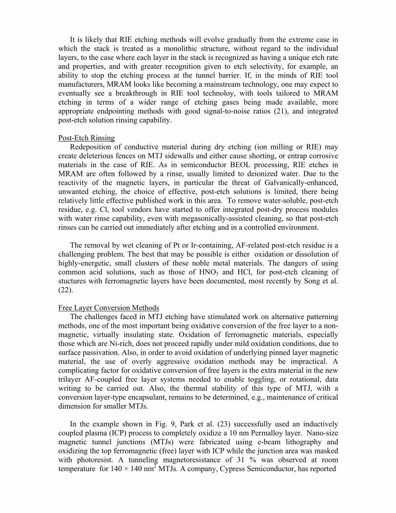
In the example shown in Fig. 9, Park et al. (23) successfully used an inductively
coupled plasma (ICP) process to completely oxidize a 10 nm Permalloy layer. Nano-size magnetic tunnel junctions (MTJs) were fabricated using e-beam lithography and oxidizing the top ferromagnetic (free) layer with ICP while the junction area was masked with photoresist. A tunneling magnetoresistance of 31 % was observed at room temperature for 140 × 140 nm2 MTJs. A company, Cypress Semiconductor, has reported
that it has developed a free layer oxidation process for MRAM MTJ patterning (24). At IBM, Abraham and O’Sullivan investigated fluorination as a means of converting thin Permalloy films (3.5 nm) to magnetically inert films (25).
Thermal Stability
Much attention has been paid to the thermal stability of MTJs, with respect to MR decrease and resistance change (the latter usually increases), due to the desire to integrate MRAM with standard back end of line (BEOL) CMOS processing, and the desire to explore applications for MRAM, such as embedded memory, with its demanding thermal annealing requirements (400 EC). Diffusion of Mn from the AF layer (Pt-Mn or Ir-Mn alloys) and FM layer/barrier interface degradation at elevated temperatures, for instance, have been concerns of several groups. However, there seems to be a lack of understanding in the MRAM field concerning modes of thermal degradation, e.g., mechanisms causing spin polarization degradation at the tunnel barrier/FM layer interfaces. This confusion is probably not helped by the range of conditions in which anneals are probably carried out, for example the presence of traces of O2 gas.
Figure 9. (a) Magnetic moment reduction of a 10 nm Permalloy layer following inductively coupled plasma (ICP) oxidation; (b) Magnetic hysteresis loop for an ebeam-patterned, 140 x 140 nm2 MTJ (23).
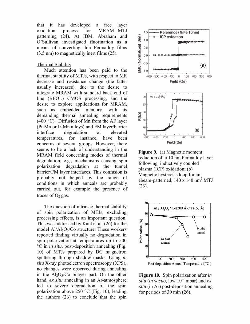
Figure 10. Spin polarization after in situ (in vacuo, low 10-9 mbar) and ex situ (in Ar) post-deposition annealing for periods of 30 min (26).
The question of intrinsic thermal stability of spin polarization of MTJs, excluding processing effects, is an important question. This was addressed by Kant et al. (26) for the model Al/Al2O3/Co structure. These workers reported finding virtually no degradation in spin polarization at temperatures up to 500 °C in in situ, post-deposition annealing (Fig. 10) of MTJs prepared by DC magnetron sputtering through shadow masks. Using in situ X-ray photoelectron spectroscopy (XPS), no changes were observed during annealing in the Al2O3/Co bilayer part. On the other hand, ex situ annealing in an Ar-atmosphere led to severe degradation of the spin polarization above 250 °C (Fig. 10), leading the authors (26) to conclude that the spin
polarization is sensitive to diffusion of impurities (in their case, derived from the Ar gas). The problem of thermal instability in practical MTJ processing is being tackled
through improvements in MTJ stack materials and careful selection of CMOS backend processing conditions and materials, e.g., through the use of low-temperature encapsulants. A number of academic researchers have employed novel, if somewhat impractical, methods to try to improve thermal stability, generally with regard to preservation of spin polarization.
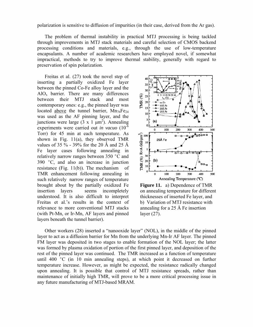
Freitas et al. (27) took the novel step of
inserting a partially oxidized Fe layer between the pinned Co-Fe alloy layer and the AlOx barrier. There are many differences between their MTJ stack and most contemporary ones: e.g., the pinned layer was located above the tunnel barrier, Mn76Fe24 was used as the AF pinning layer, and the junctions were large (3 x 1 µm2). Annealing experiments were carried out in vacuo (10-6 Torr) for 45 min at each temperature. As shown in Fig. 11(a), they observed TMR values of 35 % - 39% for the 20 Ǻ and 25 Å Fe layer cases following annealing in relatively narrow ranges between 350 EC and 390 EC, and also an increase in junction resistance (Fig. 11(b)). The mechanism of TMR enhancement following annealing in such relatively narrow ranges of temperature brought about by the partially oxidized Fe insertion layers seems incompletely understood. It is also difficult to interpret Freitas et al.’s results in the context of relevance to more conventional MTJ stacks (with Pt-Mn, or Ir-Mn, AF layers and pinned layers beneath the tunnel barrier).
Figure 11. a) Dependence of TMR on annealing temperature for different thicknesses of inserted Fe layer, and b) Variation of MTJ resistance with annealing for a 25 Å Fe insertion layer (27).
Other workers (28) inserted a “nanooxide layer” (NOL), in the middle of the pinned
layer to act as a diffusion barrier for Mn from the underlying Mn-Ir AF layer. The pinned FM layer was deposited in two stages to enable formation of the NOL layer; the latter was formed by plasma oxidation of portion of the first pinned layer, and deposition of the rest of the pinned layer was continued. The TMR increased as a function of temperature until 400 EC (in 10 min annealing steps), at which point it decreased on further temperature increase. However, as might be expected, the resistance radically changed upon annealing. It is possible that control of MTJ resistance spreads, rather than maintenance of initially high TMR, will prove to be a more critical processing issue in any future manufacturing of MTJ-based MRAM.
CONCLUSIONS
Magnetic tunnel junction research and development aimed at developing fast, nonvolatile MRAM memory continues to grow at a rapid pace. It seems likely that further significant increases in the TMR signal (now at 220 % at room temperature (4)) will be achieved, driven by improvements in MTJ stack materials and deposition tools. The need to decrease data writing currents is emerging as a strategic focus activity for MTJ-based MRAM, with cladding of bit and word lines with ferromagnetic liners as scaling is pursued being perhaps only a short term solution; the development of alternative writing methods, with lower power requirements than the toggle writing method, such as spin torque transfer is expected to continue.
Future processing enhancements for MTJ-based MRAM will include: further
tweaking of ion milling for stack patterning; developing RIE etch processes, and possibly tools, that are more tailored toward MTJ stack etching, especially improving etch selectivity to individual stack layers; given the present level of uncertainty surrounding MTJ etch patterning, exploring alternative patterning methods to etching, such as chemical conversion of the free layer to a magnetically inert and insulating state; and continued emphasis on improving thermal stability (to around 400 EC).
Competition to MRAM may come from rapidly developing, lower-speed memories
such as phase change (PCM). However, in the longer term, the experience gained from working with MTJ-based MRAM, particularly if further major gains in TMR are achieved, should give impetus to the study of spin-based devices beyond memory.
ACKNOWLEDGEMENTS
The author gratefully acknowledges discussions with, and support of, all the members
of the IBM-Infineon MRAM Development Alliance, and partial financial support from DARPA.
REFERENCES 1. S.S.P. Parkin et al., Proc. IEEE, 91, 661 (2003). 2. M. Julliere, Phys. Lett. A, 54, 225 (1975). 3. S. Yuasa et al., Nature Materials, 3, 868 (2004). 4. S.S.P. Parkin et al., Nature Materials, 3, 862 (2004). 5. E.C. Stoner and E.P. Wohlfarth, Philos. Trans. London A, 240, 599 (1948). 6. M. Durlam et al., IEDM Tech. Digest, 995 (2003). 7. J.C. Slonczewski, J. Magn. Magn. Mater., 59, L1 (1996). 8. L. Berger, Phys. Rev. B, 54, 9353 (1996). 9. J.Z. Sun et al., Proc. SPIE, 5359, 445 (2004). 10. T. Andre et al., IEEE Int. Solid-State Circuits Conf., Feb. 15 – 19, 2004, paper 2.3,
San Francisco, CA.
11. A. Bette et al., VLSI Circuits, 2003, Digest of Tech. Papers, p. 217, (2003). 12. J. DeBrosse et al., VLSI Circuits, 2004, Digest of Technical Papers p. 454, (2004). 13. D. Gogl et al., IEEE J. Solid-State Circuits (in press). 14. K.B. Jung et al., J. Electron. Mater., 27, 972 (1998). 15. K.B. Jung et al., J. Vac.Sci. Tech. A, 15, 1780 (1997). 16. K.B. Jung et al., J. Electrochem. Soc., 146, 1465 (1999). 17. R. Hsiao, IBM J. Res. Develop., 43, 89 (1999). 18. See, e.g., M. Matsui et al., Vacuum, 66, 479 (2002). 19. T. Osada et al., DPS 2004: 26th Int. Symp. Dry Process, paper P-22, Tokyo, Japan,
Nov. 30 – Dec. 1, 2004; see also the World Wide Web page http://www.anelva.co.jp/english/news/products/mram.html; last viewed 12-10-04).
20. S. Kumagi et al., J. Vac. Sci. Tech. A, 22, 1093 (2004)). 21. See, e.g., R.B. Young et al., J. Electron. Mater., 31, 994 (2002). 22. Y.S. Song et al., Electrochem. Solid-State Letts., 7, C66 (2004). 23. S.Y. Park et al., Phys. Stat. Sol. (A), 201(8), 1692 (2004). 24. E. Chen et al., J. Appl. Phys., 93(10), 8379 (2003). 25. D.W. Abraham and E.J. O’Sullivan, unpublished results; US patent applied for. 26. C.H. Kant et al., Appl. Phys. Lett., 84, 1141 (2004). 27. See, e.g., Freitas and coworkers., J. Magn. Magn. Mater., 261, L305-L310 (2003),
and refs. therein. 28. S.Y. Yoon et al., Phys. Stat. Sol. (A), 201, 1716 (2004)

Key Words
MRAM, oxide, passive film, magnetic, Permalloy, etch, selective etch, wet cleans, reactive ion etching, RIE, alumina, MgO, MTJ, magnetic tunnel junction, memory, tantalum, tunneling, hysteresis, alloy, toggle, rotation, halogen, chlorine.