IBM PowerPC 750CX/750CXe RISC Microprocessor User’s...
579
IBM PowerPC ® 750CX/750CXe RISC Microprocessor User’s Manual Version: 1.1 May 9, 2002
Transcript of IBM PowerPC 750CX/750CXe RISC Microprocessor User’s...

User’s Manual
Version: 1.1
May 9, 2002

Copyright and Disclaimer Copyright International Business Machines Corporation 2000-2002All Rights Reserved
Printed in the United States of America May 2002
The following are trademarks of International Business Machines Corporation in the United States, or other countries, or both.IBM IBM LogoPowerPC PowerPC LogoPowerPC Architecture PowerPC 750PowerPC 750CX
Other company, product and service names may be trademarks or service marks of others.
All information contained in this document is subject to change without notice. The products described in this document are NOT intended for use in implantation or other life support, space, nuclear, or military applications where malfunction may result in injury or death to persons. The information contained in this document does not affect or change IBM product specifications or warranties. Nothing in this document shall operate as an express or implied license or indemnity under the intellectual property rights of IBM or third parties. All information contained in this document was obtained in specific environments, and is presented as an illustration. The results obtained in other operating environments may vary.
THE INFORMATION CONTAINED IN THIS DOCUMENT IS PROVIDED ON AN "AS IS" BASIS. In no event will IBM be liable for damages arising directly or indirectly from any use of the information contained in this document.ned in this document.
IBM Microelectronics Division1580 Route 52, Bldg. 504Hopewell Junction, NY 12533-6351
The IBM home page can be found athttp://www.ibm.com
The IBM Microelectronics Division home pagecan be found at http://www.chips.ibm.com
750cx_um_title.fm.1.1May 9, 2002

CONTENTS
Chapter 1 PowerPC 750CX Overview1.1—750CX Microprocessor Overview ................................................................................... 1-11.2—750CX Microprocessor Features ..................................................................................... 1-4
1.2.1—Overview of 750CX Microprocessor Features ..................................................... 1-41.2.2—Instruction Flow.................................................................................................... 1-7
1.2.2.1—Instruction Queue and Dispatch Unit...................................................... 1-71.2.2.2—Branch Processing Unit (BPU) ............................................................... 1-71.2.2.3—Completion Unit ..................................................................................... 1-8
1.2.2.3.1—Independent Execution Units................................................... 1-91.2.2.3.2—Integer Units (IUs) ................................................................... 1-91.2.2.3.3—Floating-Point Unit (FPU) ....................................................... 1-91.2.2.3.4—Load/Store Unit (LSU) .......................................................... 1-101.2.2.3.5—System Register Unit (SRU).................................................. 1-10
1.2.3—Memory Management Units (MMUs) ................................................................ 1-101.2.4—On-Chip Level 1 Instruction and Data Caches ................................................... 1-111.2.5—On-Chip Level 2 Cache Implementation ............................................................ 1-131.2.6—System Interface/Bus Interface Unit (BIU) ........................................................ 1-131.2.7—Signals................................................................................................................. 1-151.2.8—Signal Configuration........................................................................................... 1-171.2.9—Clocking.............................................................................................................. 1-17
1.3—750CX Microprocessor: Implementation ...................................................................... 1-181.4—PowerPC Registers and Programming Model ............................................................... 1-201.5—Instruction Set ................................................................................................................ 1-24
1.5.1—PowerPC Instruction Set ..................................................................................... 1-251.5.2—750CX Microprocessor Instruction Set .............................................................. 1-26
1.6—On-Chip Cache Implementation .................................................................................... 1-261.6.1—PowerPC Cache Model ....................................................................................... 1-261.6.2— 750CX Microprocessor Cache Implementation ................................................ 1-27
1.7—Exception Model ............................................................................................................ 1-271.7.1—PowerPC Exception Model................................................................................. 1-271.7.2—750CX Microprocessor Exception Implementation ........................................... 1-28
1.8—Memory Management .................................................................................................... 1-301.8.1—PowerPC Memory Management Model ............................................................. 1-301.8.2— 750CX Microprocessor Memory Management Implementation....................... 1-31
1.9—Instruction Timing ......................................................................................................... 1-311.10—Power Management ..................................................................................................... 1-331.11—Thermal Management .................................................................................................. 1-341.12—Performance Monitor ................................................................................................... 1-35
Table of Contents 5/9/02 Page iii

Chapter 2 Programming Model2.1—The PowerPC 750CX Processor Register Set .................................................................. 2-1
2.1.1—Register Set ........................................................................................................... 2-12.1.2—PowerPC 750CX-Specific Registers .................................................................... 2-8
2.1.2.1—Instruction Address Breakpoint Register (IABR)................................... 2-82.1.2.2—Hardware Implementation-Dependent Register 0 .................................. 2-82.1.2.3—Hardware Implementation-Dependent Register 1 ................................ 2-132.1.2.4—Performance Monitor Registers ............................................................ 2-13
2.1.2.4.1—Monitor Mode Control Register 0 (MMCR0) ....................... 2-132.1.2.4.2—User Monitor Mode Control Register 0 (UMMCR0)............ 2-152.1.2.4.3—Monitor Mode Control Register 1 (MMCR1) ....................... 2-152.1.2.4.4—User Monitor Mode Control Register 1 (UMMCR1)............ 2-162.1.2.4.5—Performance Monitor Counter Registers (PMC1–PMC4)..... 2-162.1.2.4.6—User Performance Monitor Counter Registers
(UPMC1–UPMC4)....................................................... 2-172.1.2.4.7—Sampled Instruction Address Register (SIA)......................... 2-172.1.2.4.8—User Sampled Instruction Address Register (USIA) ............. 2-172.1.2.4.9—Sampled Data Address Register (SDA) and User Sampled Data
Address Register (USDA) ............................................ 2-172.1.3—Instruction Cache Throttling Control Register (ICTC)....................................... 2-182.1.4—Thermal Management Registers (THRM1–THRM3) ........................................ 2-182.1.5—L2 Cache Control Register (L2CR) .................................................................... 2-21
2.2—Operand Conventions .................................................................................................... 2-222.2.1—Data Organization in Memory and Data Transfers............................................. 2-232.2.2—Alignment and Misaligned Accesses .................................................................. 2-232.2.3—Floating-Point Operand and Execution Models—UISA .................................... 2-24
2.3—Instruction Set Summary ............................................................................................... 2-262.3.1—Classes of Instructions ........................................................................................ 2-27
2.3.1.1—Definition of Boundedly Undefined ..................................................... 2-272.3.1.2—Defined Instruction Class...................................................................... 2-282.3.1.3—Illegal Instruction Class ........................................................................ 2-282.3.1.4—Reserved Instruction Class.................................................................... 2-29
2.3.2—Addressing Modes .............................................................................................. 2-292.3.2.1—Memory Addressing ............................................................................. 2-292.3.2.2—Memory Operands ................................................................................ 2-292.3.2.3—Effective Address Calculation .............................................................. 2-302.3.2.4—Synchronization .................................................................................... 2-30
2.3.2.4.1—Context Synchronization........................................................ 2-302.3.2.4.2—Execution Synchronization .................................................... 2-302.3.2.4.3—Instruction-Related Exceptions.............................................. 2-31
2.3.3—Instruction Set Overview .................................................................................... 2-312.3.4—PowerPC UISA Instructions ............................................................................... 2-32
2.3.4.1—Integer Instructions ............................................................................... 2-322.3.4.1.1—Integer Arithmetic Instructions .............................................. 2-322.3.4.1.2—Integer Compare Instructions................................................. 2-342.3.4.1.3—Integer Logical Instructions ................................................... 2-34
Page iv Version 1.1 IBM PowerPC 750CX/750CXe RISC Microprocessor User’s Manual

2.3.4.1.4—Integer Rotate Instructions..................................................... 2-352.3.4.1.5—Integer Shift Instructions ....................................................... 2-36
2.3.4.2—Floating-Point Instructions ................................................................... 2-362.3.4.2.1—Floating-Point Arithmetic Instructions .................................. 2-372.3.4.2.2—Floating-Point Multiply-Add Instructions ............................. 2-372.3.4.2.3—Floating-Point Rounding and Conversion Instructions ......... 2-382.3.4.2.4—Floating-Point Compare Instructions..................................... 2-382.3.4.2.5—Floating-Point Status and Control Register Instructions ....... 2-382.3.4.2.6—Floating-Point Move Instructions .......................................... 2-39
2.3.4.3—Load and Store Instructions .................................................................. 2-402.3.4.3.1—Self-Modifying Code ............................................................. 2-402.3.4.3.2—Integer Load and Store Address Generation.......................... 2-412.3.4.3.3—Integer Load Instructions ....................................................... 2-412.3.4.3.4—Integer Store Instructions....................................................... 2-422.3.4.3.5—Integer Store Gathering.......................................................... 2-432.3.4.3.6—Integer Load and Store with Byte-Reverse Instructions ........ 2-432.3.4.3.7—Integer Load and Store Multiple Instructions ........................ 2-442.3.4.3.8—Integer Load and Store String Instructions ............................ 2-442.3.4.3.9—Floating-Point Load and Store Address Generation .............. 2-452.3.4.3.10—Floating-Point Load Instructions ......................................... 2-462.3.4.3.11—Floating-Point Store Instructions ......................................... 2-46
2.3.4.4—Branch and Flow Control Instructions.................................................. 2-492.3.4.4.1—Branch Instruction Address Calculation ................................ 2-492.3.4.4.2—Branch Instructions ................................................................ 2-492.3.4.4.3—Condition Register Logical Instructions ................................ 2-502.3.4.4.4—Trap Instructions .................................................................... 2-50
2.3.4.5—System Linkage Instruction—UISA..................................................... 2-512.3.4.6—Processor Control Instructions—UISA ................................................ 2-51
2.3.4.6.1—Move to/from Condition Register Instructions ...................... 2-512.3.4.6.2—Move to/from Special-Purpose Register Instructions (UISA)2-51
2.3.4.7—Memory Synchronization Instructions—UISA .................................... 2-542.3.5—PowerPC VEA Instructions ................................................................................ 2-55
2.3.5.1—Processor Control Instructions—VEA.................................................. 2-562.3.5.2—Memory Synchronization Instructions—VEA ..................................... 2-562.3.5.3—Memory Control Instructions—VEA ................................................... 2-57
2.3.5.3.1—User-Level Cache Instructions—VEA .................................. 2-572.3.5.4—Optional External Control Instructions................................................. 2-59
2.3.6—PowerPC OEA Instructions ................................................................................ 2-602.3.6.1—System Linkage Instructions—OEA .................................................... 2-602.3.6.2—Processor Control Instructions—OEA.................................................. 2-612.3.6.3—Memory Control Instructions—OEA ................................................... 2-61
2.3.6.3.1—Supervisor-Level Cache Management Instruction—(OEA).. 2-622.3.6.3.2—Segment Register Manipulation Instructions (OEA)............. 2-622.3.6.3.3—Translation Lookaside Buffer Management
Instructions—(OEA) .................................................... 2-632.3.7—Recommended Simplified Mnemonics............................................................... 2-63
Table of Contents 5/9/02 Page v

Chapter 3 The 750CX Instruction and Data Cache Operation3.1—Data Cache Organization ................................................................................................. 3-33.2—Instruction Cache Organization ....................................................................................... 3-43.3—Memory and Cache Coherency ........................................................................................ 3-5
3.3.1—Memory/Cache Access Attributes (WIMG Bits).................................................. 3-63.3.2—MEI Protocol......................................................................................................... 3-7
3.3.2.1—MEI Hardware Considerations ............................................................... 3-83.3.3—Coherency Precautions in Single Processor Systems ........................................... 3-93.3.4—Coherency Precautions in Multiprocessor Systems............................................ 3-103.3.5—PowerPC 750CX-Initiated Load/Store Operations............................................. 3-10
3.3.5.1—Performed Loads and Stores ................................................................. 3-103.3.5.2—Sequential Consistency of Memory Accesses ...................................... 3-103.3.5.3—Atomic Memory References ................................................................. 3-11
3.4—Cache Control ................................................................................................................ 3-123.4.1—Cache Control Parameters in HID0 .................................................................... 3-12
3.4.1.1—Data Cache Flash Invalidation.............................................................. 3-123.4.1.2—Data Cache Enabling/Disabling............................................................ 3-123.4.1.3—Data Cache Locking.............................................................................. 3-123.4.1.4—Instruction Cache Flash Invalidation .................................................... 3-133.4.1.5—Instruction Cache Enabling/Disabling .................................................. 3-133.4.1.6—Instruction Cache Locking.................................................................... 3-13
3.4.2—Cache Control Instructions ................................................................................. 3-143.4.2.1—Data Cache Block Touch (dcbt) and Data Cache Block Touch for
Store (dcbtst)............................................................................... 3-143.4.2.2—Data Cache Block Zero (dcbz) ............................................................. 3-143.4.2.3—Data Cache Block Store (dcbst) ........................................................... 3-153.4.2.4—Data Cache Block Flush (dcbf) ............................................................ 3-153.4.2.5—Data Cache Block Invalidate (dcbi) ..................................................... 3-163.4.2.6—Instruction Cache Block Invalidate (icbi)............................................. 3-16
3.5—Cache Operations ........................................................................................................... 3-163.5.1—Cache Block Replacement/Castout Operations .................................................. 3-163.5.2—Cache Flush Operations ...................................................................................... 3-193.5.3—Data Cache-Block-Fill Operations...................................................................... 3-193.5.4—Instruction Cache-Block-Fill Operations............................................................ 3-193.5.5—Data Cache-Block-Push Operation ..................................................................... 3-19
3.6—L1 Caches and 60x Bus Transactions ............................................................................ 3-193.6.1—Read Operations and the MEI Protocol .............................................................. 3-203.6.2—Bus Operations Caused by Cache Control Instructions...................................... 3-213.6.3—Snooping ............................................................................................................. 3-223.6.4—Snoop Response to 60x Bus Transactions .......................................................... 3-233.6.5—Transfer Attributes .............................................................................................. 3-26
3.7—MEI State Transactions .................................................................................................. 3-28
Page vi Version 1.1 IBM PowerPC 750CX/750CXe RISC Microprocessor User’s Manual

Chapter 4 Exceptions4.1—PowerPC 750CX Microprocessor Exceptions ................................................................. 4-24.2—Exception Recognition and Priorities .............................................................................. 4-44.3—Exception Processing ....................................................................................................... 4-7
4.3.1—Enabling and Disabling Exceptions .................................................................... 4-104.3.2—Steps for Exception Processing........................................................................... 4-104.3.3—Setting MSR[RI] ................................................................................................. 4-114.3.4—Returning from an Exception Handler................................................................ 4-11
4.4—Process Switching .......................................................................................................... 4-114.5—Exception Definitions .................................................................................................... 4-12
4.5.1—System Reset Exception (0x00100) .................................................................... 4-134.5.1.1—Soft Reset .............................................................................................. 4-134.5.1.2—Hard Reset............................................................................................. 4-14
4.5.2—Machine Check Exception (0x00200) ................................................................ 4-164.5.2.1—Machine Check Exception Enabled (MSR[ME] = 1)........................... 4-174.5.2.2—Checkstop State (MSR[ME] = 0).......................................................... 4-18
4.5.3—DSI Exception (0x00300) ................................................................................... 4-184.5.4—ISI Exception (0x00400)..................................................................................... 4-184.5.5—External Interrupt Exception (0x00500) ............................................................. 4-194.5.6—Alignment Exception (0x00600) ........................................................................ 4-194.5.7—Program Exception (0x00700)............................................................................ 4-194.5.8—Floating-Point Unavailable Exception (0x00800) .............................................. 4-204.5.9—Decrementer Exception (0x00900) ..................................................................... 4-204.5.10—System Call Exception (0x00C00) ................................................................... 4-204.5.11—Trace Exception (0x00D00).............................................................................. 4-204.5.12—Floating-Point Assist Exception (0x00E00) ..................................................... 4-214.5.13—Performance Monitor Interrupt (0x00F00) ....................................................... 4-214.5.14—Instruction Address Breakpoint Exception (0x01300) ..................................... 4-224.5.15—Thermal Management Interrupt Exception (0x01700) ..................................... 4-23
Chapter 5 Memory Management5.1—MMU Overview ............................................................................................................... 5-1
5.1.1—Memory Addressing ............................................................................................. 5-35.1.2—MMU Organization............................................................................................... 5-35.1.3—Address Translation Mechanisms......................................................................... 5-85.1.4—Memory Protection Facilities.............................................................................. 5-105.1.5—Page History Information.................................................................................... 5-115.1.6—General Flow of MMU Address Translation ...................................................... 5-11
5.1.6.1—Real Addressing Mode and Block Address Translation Selection ....... 5-115.1.6.2—Page Address Translation Selection ..................................................... 5-12
5.1.7—MMU Exceptions Summary ............................................................................... 5-155.1.8—MMU Instructions and Register Summary ......................................................... 5-17
5.2—Real Addressing Mode ................................................................................................... 5-185.3—Block Address Translation ............................................................................................. 5-195.4—Memory Segment Model ............................................................................................... 5-19
Table of Contents 5/9/02 Page vii

5.4.1—Page History Recording ...................................................................................... 5-205.4.1.1—Referenced Bit ...................................................................................... 5-205.4.1.2—Changed Bit .......................................................................................... 5-215.4.1.3—Scenarios for Referenced and Changed Bit Recording ........................ 5-21
5.4.2—Page Memory Protection .................................................................................... 5-225.4.3—TLB Description ................................................................................................. 5-22
5.4.3.1—TLB Organization ................................................................................. 5-235.4.3.2—TLB Invalidation................................................................................... 5-26
5.4.4—Page Address Translation Summary................................................................... 5-265.4.5—Page Table Search Operation.............................................................................. 5-285.4.6—Page Table Updates ............................................................................................ 5-325.4.7—Segment Register Updates .................................................................................. 5-32
Chapter 6 Instruction Timing6.1—Terminology and Conventions ......................................................................................... 6-16.2—Instruction Timing Overview ........................................................................................... 6-36.3—Timing Considerations ..................................................................................................... 6-6
6.3.1—General Instruction Flow ...................................................................................... 6-86.3.2—Instruction Fetch Timing ...................................................................................... 6-9
6.3.2.1—Cache Arbitration.................................................................................... 6-96.3.2.2—Cache Hit ................................................................................................ 6-96.3.2.3—Cache Miss............................................................................................ 6-146.3.2.4—L2 Cache Access Timing Considerations ............................................. 6-166.3.2.5—Instruction Dispatch and Completion Considerations .......................... 6-166.3.2.6—Rename Register Operation .................................................................. 6-176.3.2.7—Instruction Serialization........................................................................ 6-17
6.4—Execution Unit Timings ................................................................................................. 6-186.4.1—Branch Processing Unit Execution Timing ........................................................ 6-18
6.4.1.1—Branch Folding ..................................................................................... 6-186.4.1.2—Branch Instructions and Completion .................................................... 6-206.4.1.3—Branch Prediction and Resolution ........................................................ 6-20
6.4.1.3.1—Static Branch Prediction ........................................................ 6-226.4.1.3.2—Predicted Branch Timing Examples ...................................... 6-22
6.4.2—Integer Unit Execution Timing ........................................................................... 6-246.4.3—Floating-Point Unit Execution Timing ............................................................... 6-246.4.4—Effect of Floating-Point Exceptions on Performance ......................................... 6-246.4.5—Load/Store Unit Execution Timing..................................................................... 6-256.4.6—Effect of Operand Placement on Performance.................................................... 6-256.4.7—Integer Store Gathering....................................................................................... 6-266.4.8—System Register Unit Execution Timing ............................................................ 6-26
6.5—Memory Performance Considerations ........................................................................... 6-276.5.1—Caching and Memory Coherency ....................................................................... 6-276.5.2—Effect of TLB Miss ............................................................................................. 6-28
6.6—Instruction Scheduling Guidelines ................................................................................. 6-286.6.1—Branch, Dispatch, and Completion Unit Resource Requirements...................... 6-29
Page viii Version 1.1 IBM PowerPC 750CX/750CXe RISC Microprocessor User’s Manual

6.6.1.1—Branch Resolution Resource Requirements ......................................... 6-296.6.1.2—Dispatch Unit Resource Requirements ................................................. 6-296.6.1.3—Completion Unit Resource Requirements ............................................ 6-30
6.7—Instruction Latency Summary ........................................................................................ 6-31
Chapter 7 Signal Descriptions7.1—Signal Configuration ........................................................................................................ 7-27.2—Signal Descriptions .......................................................................................................... 7-2
7.2.1—Address Bus Arbitration Signals........................................................................... 7-37.2.1.1—Bus Request (BR)—Output .................................................................... 7-37.2.1.2—Bus Grant (BG)—Input .......................................................................... 7-3
7.2.2—Address Transfer Start Signals ............................................................................. 7-47.2.2.1—Transfer Start (TS).................................................................................. 7-4
7.2.2.1.1—Transfer Start (TS)—Output.................................................... 7-47.2.2.1.2—Transfer Start (TS)—Input ...................................................... 7-4
7.2.3—Address Transfer Signals ...................................................................................... 7-47.2.3.1—Address Bus (A[0–31]) ........................................................................... 7-4
7.2.3.1.1—Address Bus (A[0–31])—Output............................................. 7-57.2.3.1.2—Address Bus (A[0–31])—Input ............................................... 7-5
7.2.3.2—Address Bus Parity (AP[0–3]) (Optional on 750CX)............................. 7-57.2.3.2.1—Address Bus Parity (AP[0–3])—Input (Optional on 750CX) . 7-5
7.2.4—Address Transfer Attribute Signals....................................................................... 7-67.2.4.1—Transfer Type (TT[0–4]) ........................................................................ 7-6
7.2.4.1.1—Transfer Type (TT[0–4])—Output .......................................... 7-67.2.4.1.2—Transfer Type (TT[0–4])—Input ............................................. 7-6
7.2.4.2—Transfer Size (TSIZ[0–2])—Output ....................................................... 7-97.2.4.3—Transfer Burst (TBST) ......................................................................... 7-10
7.2.4.3.1—Transfer Burst (TBST)—Output ........................................... 7-107.2.4.3.2—Transfer Burst (TBST)—Input .............................................. 7-10
7.2.4.4—Cache Inhibit (CI)—Output.................................................................. 7-107.2.4.5—Write-Through (WT)—Output ............................................................. 7-107.2.4.6—Global (GBL)........................................................................................ 7-11
7.2.4.6.1—Global (GBL)—Output.......................................................... 7-117.2.4.6.2—Global (GBL)—Input ............................................................ 7-11
7.2.5—Address Transfer Termination Signals ............................................................... 7-117.2.5.1—Address Acknowledge (AACK)—Input .............................................. 7-117.2.5.2—Address Retry (ARTRY) ...................................................................... 7-12
7.2.5.2.1—Address Retry (ARTRY)—Output ........................................ 7-127.2.5.2.2—Address Retry (ARTRY)—Input........................................... 7-12
7.2.6—Data Bus Arbitration Signals .............................................................................. 7-127.2.6.1—Data Bus Grant (DBG)—Input............................................................. 7-13
7.2.7—Data Transfer Signals.......................................................................................... 7-137.2.7.1—Data Bus (DH[0–31], DL[0–31]).......................................................... 7-13
7.2.7.1.1—Data Bus (DH[0–31], DL[0–31])—Output ........................... 7-147.2.7.1.2—Data Bus (DH[0–31], DL[0–31])—Input .............................. 7-14
Table of Contents 5/9/02 Page ix

7.2.7.2—Data Bus Parity (DP[0–7]) (Optional on 750CX) ................................ 7-147.2.7.2.1—Data Bus Parity (DP[0–7])—Output...................................... 7-147.2.7.2.2—Data Bus Parity (DP[0–7])—Input ........................................ 7-15
7.2.8—Data Transfer Termination Signals..................................................................... 7-157.2.8.1—Transfer Acknowledge (TA)—Input .................................................... 7-157.2.8.2—Data Retry (DRTRY)—Input (Optional on 750CX) ............................ 7-157.2.8.3—Transfer Error Acknowledge (TEA)—Input ........................................ 7-16
7.2.9—System Status Signals ......................................................................................... 7-167.2.9.1—Interrupt (INT)— Input ........................................................................ 7-167.2.9.2—Machine Check Interrupt (MCP)—Input ............................................. 7-177.2.9.3—Checkstop Input (CKSTP_IN)—Input................................................. 7-177.2.9.4—Checkstop Output (CKSTP_OUT)—Output ....................................... 7-177.2.9.5—Reset Signals......................................................................................... 7-18
7.2.9.5.1—Hard Reset (HRESET)—Input .............................................. 7-187.2.9.5.2—Soft Reset (SRESET)—Input ................................................ 7-18
7.2.9.6—Processor Status Signals ....................................................................... 7-197.2.9.6.1—Quiescent Request (QREQ)—Output.................................... 7-197.2.9.6.2—Quiescent Acknowledge (QACK)—Input ............................ 7-197.2.9.6.3—TLBI Sync (TLBISYNC)—Input (Optional on 750CX) ...... 7-19
7.2.10—IEEE 1149.1a-1993 Interface Description........................................................ 7-207.2.11—Clock Signals .................................................................................................... 7-20
7.2.11.1—System Clock (SYSCLK)—Input....................................................... 7-207.2.11.2—Clock Out (CLK_OUT)—Output (N/A on the 750CX)..................... 7-217.2.11.3—PLL Configuration (PLL_CFG[0–3])—Input .................................... 7-21
7.2.12—Power and Ground Signals ............................................................................... 7-21
Chapter 8 Bus Interface Operation8.1—Bus Interface Overview ................................................................................................... 8-2
8.1.1—Operation of the Instruction and Data L1 Caches................................................. 8-38.1.2—Operation of the Bus Interface.............................................................................. 8-68.1.3—Direct-Store Accesses ........................................................................................... 8-6
8.2—Memory Access Protocol ................................................................................................. 8-78.2.1—Arbitration Signals ................................................................................................ 8-98.2.2—Address Pipelining and Split-Bus Transactions.................................................... 8-9
8.3—Address Bus Tenure ....................................................................................................... 8-108.3.1—Address Bus Arbitration ..................................................................................... 8-108.3.2—Address Transfer................................................................................................. 8-13
8.3.2.1—Address Bus Parity (Parity is optional on the 750CX) ......................... 8-148.3.2.2—Address Transfer Attribute Signals....................................................... 8-14
8.3.2.2.1—Transfer Type (TT[0–4]) Signals........................................... 8-148.3.2.2.2—Transfer Size (TSIZ[0–2]) Signals ........................................ 8-148.3.2.2.3—Write-Through (WT) Signal .................................................. 8-158.3.2.2.4—Cache Inhibit (CI) Signal ....................................................... 8-15
8.3.2.3—Burst Ordering During Data Transfers ................................................. 8-158.3.2.4—Effect of Alignment in Data Transfers ................................................. 8-16
Page x Version 1.1 IBM PowerPC 750CX/750CXe RISC Microprocessor User’s Manual

8.3.2.5—Alignment of External Control Instructions ......................................... 8-188.3.3—Address Transfer Termination ............................................................................ 8-18
8.4—Data Bus Tenure ............................................................................................................ 8-198.4.1—Data Bus Arbitration ........................................................................................... 8-208.4.2—Data Transfer ...................................................................................................... 8-218.4.3—Data Transfer Termination.................................................................................. 8-21
8.4.3.1—Normal Single-Beat Termination.......................................................... 8-228.4.3.2—Data Transfer Termination Due to a Bus Error .................................... 8-25
8.4.4—Memory Coherency—MEI Protocol .................................................................. 8-258.5—Timing Examples ........................................................................................................... 8-278.6—No-DRTRY Bus Configuration(DRTRY is optional on the 750CX) ............................ 8-338.7—32-bit Data Bus Mode .................................................................................................... 8-338.8—Interrupt, Checkstop, and Reset Signals ........................................................................ 8-37
8.8.1—External Interrupts .............................................................................................. 8-378.8.2—Checkstops .......................................................................................................... 8-378.8.3—Reset Inputs......................................................................................................... 8-388.8.4—System Quiesce Control Signals......................................................................... 8-38
8.9—Processor State Signals .................................................................................................. 8-398.9.1—Support for the lwarx/stwcx. Instruction Pair .................................................... 8-398.9.2—TLBISYNC Input (Optional on the 750CX)...................................................... 8-39
8.10—IEEE 1149.1a-1993 Compliant Interface ..................................................................... 8-398.10.1—JTAG/COP Interface......................................................................................... 8-39
Chapter 9 L2 Cache9.1—L2 Cache Overview ......................................................................................................... 9-1
9.1.1—L2 Cache Operation .............................................................................................. 9-19.1.2—L2 Cache Control Register (L2CR) ...................................................................... 9-49.1.3—L2 Cache Initialization.......................................................................................... 9-49.1.4—L2 Cache Global Invalidation............................................................................... 9-59.1.5—L2 Cache Test Features and Methods................................................................... 9-5
9.1.5.1—L2CR Support for L2 Cache Testing...................................................... 9-69.1.5.2—L2 Cache Testing .................................................................................... 9-6
9.1.6—L2 Cache Timing .................................................................................................. 9-7
Chapter 10 Power and Thermal Management10.1—Dynamic Power Management ...................................................................................... 10-110.2—Programmable Power Modes ....................................................................................... 10-1
10.2.1—Power Management Modes .............................................................................. 10-210.2.1.1—Full-Power Mode ................................................................................ 10-210.2.1.2—Doze Mode.......................................................................................... 10-210.2.1.3—Nap Mode ........................................................................................... 10-310.2.1.4—Sleep Mode ......................................................................................... 10-4
10.2.2—Power Management Software Considerations .................................................. 10-510.3—Thermal Assist Unit ..................................................................................................... 10-5
10.3.1—Thermal Assist Unit Overview ......................................................................... 10-6
Table of Contents 5/9/02 Page xi

10.3.2—Thermal Assist Unit Operation ......................................................................... 10-810.3.2.1—TAU Single Threshold Mode ............................................................. 10-810.3.2.2—TAU Dual-Threshold Mode................................................................ 10-910.3.2.3—750CX Junction Temperature Determination................................... 10-1010.3.2.4—Power Saving Modes and TAU Operation ....................................... 10-10
10.4—Instruction Cache Throttling ...................................................................................... 10-10
Chapter 11 Performance Monitor11.1—Performance Monitor Interrupt .................................................................................... 11-111.2—Special-Purpose Registers Used by Performance Monitor .......................................... 11-2
11.2.1—Performance Monitor Registers ........................................................................ 11-311.2.1.1—Monitor Mode Control Register 0 (MMCR0) .................................... 11-311.2.1.2—User Monitor Mode Control Register 0 (UMMCR0)......................... 11-511.2.1.3—Monitor Mode Control Register 1 (MMCR1) .................................... 11-511.2.1.4—User Monitor Mode Control Register 1 (UMMCR1)......................... 11-511.2.1.5—Performance Monitor Counter Registers (PMC1–PMC4).................. 11-511.2.1.6—User Performance Monitor Counter Registers (UPMC1–UPMC4) ... 11-911.2.1.7—Sampled Instruction Address Register (SIA).................................... 11-1011.2.1.8—User Sampled Instruction Address Register (USIA) ........................ 11-10
11.3—Event Counting .......................................................................................................... 11-1011.4—Event Selection .......................................................................................................... 11-1111.5—Notes .......................................................................................................................... 11-12
Chapter 12 Instruction Set12.1—Instruction Formats ...................................................................................................... 12-1
12.1.1—Split-Field Notation .......................................................................................... 12-112.1.2—Instruction Fields .............................................................................................. 12-212.1.3—Notation and Conventions ................................................................................ 12-412.1.4—Computation Modes.......................................................................................... 12-7
12.2—PowerPC Instruction Set .............................................................................................. 12-8
Appendix A 750CX Instruction SetA.1—Instructions Sorted by Opcode.................................................................................. A-1A.2—Instructions Grouped by Functional Categories ....................................................... A-7
Revision Log 1
Index
Page xii Version 1.1 IBM PowerPC 750CX/750CXe RISC Microprocessor User’s Manual

TABLES
Chapter 1—PowerPC 750CX OverviewTable 1-2 Architecture-Defined SPRs Implemented .................................................................... 1-23Table 1-3 Implementation-Specific Registers .............................................................................. 1-24Table 1-4 750CX Microprocessor Exception Classifications ....................................................... 1-29Table 1-5 Exceptions and Conditions ........................................................................................... 1-29
Chapter 2—Programming ModelTable 2-1. Additional MSR Bits ..................................................................................................... 2-4Table 2-2. Additional SRR1 Bits .................................................................................................... 2-6Table 2-3. Instruction Address Breakpoint Register Bit Settings ................................................... 2-8Table 2-4. HID0 Bit Functions ....................................................................................................... 2-9Table 2-5. HID0[BCLK] and HID0[ECLK] CKSTP_OUT Configuration ................................. 2-12Table 2-6. HID1 Bit Functions ..................................................................................................... 2-13Table 2-7. MMCR0 Bit Settings ................................................................................................... 2-14Table 2-8. MMCR1 Bits ............................................................................................................... 2-15Table 2-9. PMCn Bits ................................................................................................................... 2-16Table 2-10. ICTC Bit Settings ...................................................................................................... 2-18Table 2-11. THRM1–THRM2 Bit Settings .................................................................................. 2-19Table 2-12. Valid THRM1/THRM2 Bit Settings ......................................................................... 2-20Table 2-13. THRM3 Bit Settings .................................................................................................. 2-21Table 2-14. L2CR Bit Settings ..................................................................................................... 2-22Table 2-15. Memory Operands ..................................................................................................... 2-23Table 2-16. Floating-Point Operand Data Type Behavior ............................................................ 2-25Table 2-17. Floating-Point Result Data Type Behavior ............................................................... 2-26Table 2-18. Integer Arithmetic Instructions ................................................................................. 2-33Table 2-19. Integer Compare Instructions .................................................................................... 2-34Table 2-20. Integer Logical Instructions ....................................................................................... 2-34Table 2-21. Integer Rotate Instructions ........................................................................................ 2-35Table 2-22. Integer Shift Instructions ........................................................................................... 2-36Table 2-23. Floating-Point Arithmetic Instructions ...................................................................... 2-37Table 2-24. Floating-Point Multiply-Add Instructions ................................................................. 2-37Table 2-25. Floating-Point Rounding and Conversion Instructions ............................................. 2-38Table 2-26. Floating-Point Compare Instructions ........................................................................ 2-38Table 2-27. Floating-Point Status and Control Register Instructions ........................................... 2-39Table 2-28. Floating-Point Move Instructions .............................................................................. 2-39Table 2-29. Integer Load Instructions ........................................................................................... 2-41Table 2-30. Integer Store Instructions .......................................................................................... 2-42Table 2-31. Integer Load and Store with Byte-Reverse Instructions ............................................ 2-44Table 2-32. Integer Load and Store Multiple Instructions ............................................................ 2-44Table 2-33. Integer Load and Store String Instructions ................................................................ 2-45Table 2-34. Floating-Point Load Instructions ............................................................................... 2-46
Table of Contents 5/9/02 Page xiii

Table 2-35. Floating-Point Store Instructions ............................................................................... 2-47Table 2-36. Store Floating-Point Single Behavior ........................................................................ 2-47Table 2-37. Store Floating-Point Double Behavior ...................................................................... 2-48Table 2-38. Branch Instructions .................................................................................................... 2-49Table 2-39. Condition Register Logical Instructions .................................................................... 2-50Table 2-40. Trap Instructions ........................................................................................................ 2-50Table 2-41. System Linkage Instruction—UISA ......................................................................... 2-51Table 2-42. Move to/from Condition Register Instructions ......................................................... 2-51Table 2-43. Move to/from Special-Purpose Register Instructions (UISA) ................................... 2-51Table 2-44. PowerPC Encodings .................................................................................................. 2-52Table 2-45. SPR Encodings for 750CX-Defined Registers (mfspr) ............................................ 2-53Table 2-46. Memory Synchronization Instructions—UISA ......................................................... 2-55Table 2-47. Move from Time Base Instruction ............................................................................ 2-56Table 2-48. Memory Synchronization Instructions—VEA .......................................................... 2-57Table 2-49. User-Level Cache Instructions .................................................................................. 2-58Table 2-50. External Control Instructions .................................................................................... 2-60Table 2-51. System Linkage Instructions—OEA ......................................................................... 2-60Table 2-52. Move to/from Machine State Register Instructions ................................................... 2-61Table 2-53. Move to/from Special-Purpose Register Instructions (OEA) .................................... 2-61Table 2-54. Supervisor-Level Cache Management Instruction .................................................... 2-62Table 2-55. Segment Register Manipulation Instructions ............................................................ 2-62Table 2-56. Translation Lookaside Buffer Management Instruction ............................................ 2-63
Chapter 3—The 750CX Instruction and Data Cache OperationTable 3-1. MEI State Definitions .................................................................................................... 3-7Table 3-2. PLRU Bit Update Rules .............................................................................................. 3-18Table 3-3. PLRU Replacement Block Selection .......................................................................... 3-18Table 3-4. Bus Operations Caused by Cache Control Instructions (WIM = 001) ........................ 3-21Table 3-5. Response to Snooped Bus Transactions ..................................................................... 3-23Table 3-6. Address/Transfer Attribute Summary ......................................................................... 3-27Table 3-7. MEI State Transitions .................................................................................................. 3-28
Chapter 4—ExceptionsTable 4-1. PowerPC 750CX Microprocessor Exception Classifications ........................................ 4-2Table 4-2. Exceptions and Conditions ............................................................................................ 4-3Table 4-3. PowerPC 750CX Exception Priorities .......................................................................... 4-5Table 4-4. MSR Bit Settings ........................................................................................................... 4-7Table 4-5. IEEE Floating-Point Exception Mode Bits ................................................................... 4-9Table 4-6. MSR Setting Due to Exception ................................................................................... 4-12Table 4-7. System Reset Exception—Register Settings ............................................................... 4-13Table 4-8. Settings Caused by Hard Reset ................................................................................... 4-15Table 4-9. HID0 Machine Check Enable Bits .............................................................................. 4-16Table 4-10. Machine Check Exception—Register Settings ......................................................... 4-17Table 4-11. Performance Monitor Interrupt Exception—Register Settings ................................. 4-22
Page xiv Version 1.1 IBM PowerPC 750CX/750CXe RISC Microprocessor User’s Manual

Table 4-12. Instruction Address Breakpoint Exception—Register Settings ................................ 4-23Table 4-13. Thermal Management Interrupt Exception—Register Settings ................................ 4-24
Chapter 5—Memory ManagementTable 5-1. MMU Feature Summary ............................................................................................... 5-2Table 5-2. Access Protection Options for Pages ........................................................................... 5-10Table 5-3. Translation Exception Conditions ............................................................................... 5-15Table 5-4. Other MMU Exception Conditions for the 750CX Processor .................................... 5-16Table 5-5. 750CX Microprocessor Instruction Summary—Control MMUs ................................ 5-17Table 5-6. 750CX Microprocessor MMU Registers .................................................................... 5-18Table 5-7. Table Search Operations to Update History Bits—TLB Hit Case .............................. 5-20Table 5-8. Model for Guaranteed R and C Bit Settings ................................................................ 5-22
Chapter 6—Instruction TimingTable 6-1. Performance Effects of Memory Operand Placement ................................................. 6-25Table 6-2. TLB Miss Latencies .................................................................................................... 6-28Table 6-3. Branch Instructions ...................................................................................................... 6-31Table 6-4. System Register Instructions ....................................................................................... 6-31Table 6-5. Condition Register Logical Instructions ...................................................................... 6-32Table 6-6. Integer Instructions ...................................................................................................... 6-33Table 6-7. Floating-Point Instructions .......................................................................................... 6-35Table 6-8. Load and Store Instructions ......................................................................................... 6-36
Chapter 7—Signal DescriptionsTable 7-1. Transfer Type Encodings for PowerPC 750CX Bus Master ......................................... 7-6Table 7-2. PowerPC 750CX Snoop Hit Response .......................................................................... 7-8Table 7-3. Data Transfer Size ......................................................................................................... 7-9Table 7-4. Data Bus Lane Assignments ........................................................................................ 7-13Table 7-5. DP[0–7] Signal Assignments ...................................................................................... 7-14Table 7-6. IEEE Interface Pin Descriptions .................................................................................. 7-20
Chapter 8—Bus Interface OperationTable 8-1. Transfer Size Signal Encodings .................................................................................. 8-14Table 8-2. Burst Ordering ............................................................................................................. 8-15Table 8-3. Aligned Data Transfers ................................................................................................ 8-16Table 8-4. Misaligned Data Transfers (Four-Byte Examples) ...................................................... 8-17Table 8-5. Burst Ordering—32-Bit Bus ....................................................................................... 8-35Table 8-6. Aligned Data Transfers (32-Bit Bus Mode) ................................................................ 8-36Table 8-7. Misaligned 32-Bit Data Bus Transfer (Four-Byte Examples) ..................................... 8-37
Table of Contents 5/9/02 Page xv

Chapter 9—L2 CacheTable 9-8. L2 Cache Control Register ............................................................................................ 9-4
Chapter 10—Power and Thermal ManagementTable 10-1. 750CX Microprocessor Programmable Power Modes .............................................. 10-2Table 10-2. THRM1 and THRM2 Bit Field Settings ................................................................... 10-7Table 10-3. THRM3 Bit Field Settings ........................................................................................ 10-7Table 10-4. Valid THRM1 and THRM2 Bit Settings .................................................................. 10-9Table 10-5. ICTC Bit Field Settings ........................................................................................... 10-11
Chapter 11— Performance MonitorTable 11-1. Performance Monitor SPRs ....................................................................................... 11-2Table 11-2. MMCR0 Bit Settings ................................................................................................. 11-3Table 11-3. MMCR1 Bit Settings ................................................................................................. 11-5Table 11-4. PMCn Bit Settings ..................................................................................................... 11-6Table 11-5. PMC1 Events—MMCR0[19–25] Select Encodings ................................................. 11-6Table 11-6. PMC2 Events—MMCR0[26–31] Select Encodings ................................................. 11-7Table 11-7. PMC3 Events—MMCR1[0–4] Select Encodings ..................................................... 11-8Table 11-8. PMC4 Events—MMCR1[5–9] Select Encodings ..................................................... 11-9
Chapter 12—Instruction SetTable 12-1. Split-Field Notation and Conventions ....................................................................... 12-1Table 12-2. Instruction Syntax Conventions ................................................................................ 12-2Table 12-3. Notation and Conventions ......................................................................................... 12-4Table 12-4. Instruction Field Conventions ................................................................................... 12-6Table 12-5. Precedence Rules ....................................................................................................... 12-7Table 12-6. BO Operand Encodings ........................................................................................... 12-23Table 12-7. BO Operand Encodings ........................................................................................... 12-25Table 12-8. BO Operand Encodings ........................................................................................... 12-27Table 12-9. PowerPC 750CX UISA SPR Encodings for mfspr .............................................. 12-127Table 12-10. PowerPC 750CX OEA SPR Encodings for mfspr ............................................. 12-128Table 12-11. TBR Encodings for mftb .................................................................................... 12-132Table 12-12. PowerPC 750CX UISA SPR Encodings for mtspr ............................................ 12-140Table 12-13. PowerPC 750CX OEA SPR Encodings for mtspr ............................................. 12-141
Appendix A—750CX Instruction SetTable A-1. Complete Instruction List Sorted by Opcode .............................................................. A-1Table A-2. Integer Arithmetic Instructions .................................................................................... A-7Table A-3. Integer Compare Instructions ...................................................................................... A-8Table A-4. Integer Logical Instructions ......................................................................................... A-8Table A-5. Integer Rotate Instructions ........................................................................................... A-8Table A-6. Integer Shift Instructions ............................................................................................. A-9Table A-7. Floating-Point Arithmetic Instructions ........................................................................ A-9Table A-8. Floating-Point Multiply-Add Instructions ................................................................... A-9
Page xvi Version 1.1 IBM PowerPC 750CX/750CXe RISC Microprocessor User’s Manual

Table A-9. Floating-Point Rounding and Conversion Instructions ............................................. A-10Table A-10. Floating-Point Compare Instructions ...................................................................... A-10Table A-11. Floating-Point Status and Control Register Instructions ......................................... A-10Table A-12. Integer Load Instructions ......................................................................................... A-11Table A-13. Integer Store Instructions ........................................................................................ A-12Table A-14. Integer Load and Store with Byte Reverse Instructions .......................................... A-12Table A-15. Integer Load and Store Multiple Instructions .......................................................... A-12Table A-16. Integer Load and Store String Instructions .............................................................. A-13Table A-17. Memory Synchronization Instructions .................................................................... A-13Table A-18. Floating-Point Load Instructions ............................................................................. A-13Table A-19. Floating-Point Store Instructions ............................................................................. A-14Table A-20. Floating-Point Move Instructions ............................................................................ A-14Table A-21. Branch Instructions .................................................................................................. A-14Table A-22. Condition Register Logical Instructions .................................................................. A-15Table A-23. System Linkage Instructions ................................................................................... A-15Table A-24. Trap Instructions ...................................................................................................... A-15Table A-25. Processor Control Instructions ................................................................................ A-16Table A-26. Cache Management Instructions ............................................................................. A-16Table A-27. Segment Register Manipulation Instructions. ......................................................... A-17Table A-28. Lookaside Buffer Management Instructions ........................................................... A-17Table A-29. External Control Instructions .................................................................................. A-17
—Index
Table of Contents 5/9/02 Page xvii
ILLUSTRATIONS
Chapter 1—PowerPC 750CX OverviewFigure 1-1. 750CX Microprocessor Block Diagram ................................................................. 1-3Figure 1-2. Cache Organization................................................................................................ 1-12Figure 1-3. System Interface .................................................................................................... 1-15Figure 1-4. 750CX Microprocessor Signal Groups.................................................................. 1-17Figure 1-5. 750CX Microprocessor Programming Model—Registers .................................... 1-21
Chapter 2—Programming ModelFigure 2-1. Programming Model—PowerPC 750CX Microprocessor Registers ...................... 2-2Figure 2-2. Instruction Address Breakpoint Register ................................................................. 2-8Figure 2-3. Hardware Implementation-Dependent Register 0 (HID0)....................................... 2-9Figure 2-4. Hardware Implementation-Dependent Register 1 (HID1)..................................... 2-13Figure 2-5. Monitor Mode Control Register 0 (MMCR0) ....................................................... 2-13Figure 2-6. Monitor Mode Control Register 1 (MMCR1) ....................................................... 2-15Figure 2-7. Performance Monitor Counter Registers (PMC1–PMC4)..................................... 2-16Figure 2-8. Sampled Instruction Address Registers (SIA) ....................................................... 2-17Figure 2-9. Instruction Cache Throttling Control Register (ICTC).......................................... 2-18Figure 2-10. Thermal Management Registers 1–2 (THRM1–THRM2) .................................... 2-19Figure 2-11. Thermal Management Register 3 (THRM3) ......................................................... 2-20Figure 2-12. L2 Cache Control Register (L2CR) ....................................................................... 2-21
Chapter 3—The 750CX Instruction and Data Cache OperationFigure 3-1. Cache Integration..................................................................................................... 3-2Figure 3-2. Data Cache Organization ......................................................................................... 3-3Figure 3-3. Instruction Cache Organization ............................................................................... 3-5Figure 3-4. MEI Cache Coherency Protocol—State Diagram (WIM = 001)............................. 3-8Figure 3-5. PLRU Replacement Algorithm.............................................................................. 3-17Figure 3-6. 750CX Cache Addresses ...................................................................................... 3-20
Chapter 4—ExceptionsFigure 4-1. Machine Status Save/Restore Register 0 (SRR0) .................................................... 4-7Figure 4-2. Machine Status Save/Restore Register 1 (SRR1) .................................................... 4-7Figure 4-3. Machine State Register (MSR) ................................................................................ 4-7Figure 4-4. SRESET Asserted During HRESET...................................................................... 4-14
Chapter 5—Memory ManagementFigure 5-1. MMU Conceptual Block Diagram........................................................................... 5-5Figure 5-2. PowerPC 750CX Microprocessor IMMU Block Diagram...................................... 5-6Figure 5-3. The 750CX Microprocessor DMMU Block Diagram ............................................. 5-7Figure 5-4. Address Translation Types ...................................................................................... 5-9
Table of Contents 5/9/02 Page xviii

Figure 5-5. General Flow of Address Translation (Real Addressing Mode and Block) .......... 5-12Figure 5-6. General Flow of Page and Direct-Store Interface Address Translation ................ 5-14Figure 5-7. Segment Register and DTLB Organization ........................................................... 5-24Figure 5-8. Page Address Translation Flow—TLB Hit ........................................................... 5-27Figure 5-9. Primary Page Table Search.................................................................................... 5-30Figure 5-10. Secondary Page Table Search Flow....................................................................... 5-31
Chapter 6—Instruction TimingFigure 6-1. Pipelined Execution Unit ......................................................................................... 6-4Figure 6-2. Superscalar/Pipeline Diagram.................................................................................. 6-4Figure 6-3. PowerPC 750CX Microprocessor Pipeline Stages .................................................. 6-7Figure 6-4. Instruction Flow Diagram...................................................................................... 6-10Figure 6-5. Instruction Timing—Cache Hit ............................................................................. 6-12Figure 6-6. Instruction Timing—Cache Miss........................................................................... 6-15Figure 6-7. Branch Taken......................................................................................................... 6-19Figure 6-8. Removal of Fall-Through Branch Instruction ....................................................... 6-19Figure 6-9. Branch Completion ................................................................................................ 6-20Figure 6-10. Branch Instruction Timing..................................................................................... 6-23
Chapter 7—Signal DescriptionsFigure 7-1. PowerPC 750CX Signal Groups.............................................................................. 7-2
Chapter 8—Bus Interface OperationFigure 8-1. Bus Interface Address Buffers ................................................................................ 8-2Figure 8-2. PowerPC 750CX Microprocessor Block Diagram .................................................. 8-5Figure 8-3. Timing Diagram Legend.......................................................................................... 8-7Figure 8-4. Overlapping Tenures on the 750CX Bus for a Single-Beat Transfer ...................... 8-8Figure 8-5. Address Bus Arbitration ........................................................................................ 8-11Figure 8-6. Address Bus Arbitration Showing Bus Parking .................................................... 8-12Figure 8-7. Address Bus Transfer............................................................................................. 8-13Figure 8-8. Snooped Address Cycle with ARTRY .................................................................. 8-19Figure 8-9. Data Bus Arbitration.............................................................................................. 8-20Figure 8-10. Normal Single-Beat Read Termination ................................................................. 8-22Figure 8-11. Normal Single-Beat Write Termination ................................................................ 8-22Figure 8-12. Normal Burst Transaction...................................................................................... 8-23Figure 8-13. Termination with DRTRY............................................................................... 8-24Figure 8-14. Read Burst with TA Wait States and DRTRY................................................... 8-24Figure 8-15. MEI Cache Coherency Protocol—State Diagram (WIM = 001)........................... 8-26Figure 8-16. Fastest Single-Beat Reads...................................................................................... 8-27Figure 8-17. Fastest Single-Beat Writes..................................................................................... 8-28Figure 8-18. Single-Beat Reads Showing Data-Delay Controls ................................................ 8-29Figure 8-19. Single-Beat Writes Showing Data Delay Controls................................................ 8-30Figure 8-20. Burst Transfers with Data Delay Controls............................................................. 8-31Figure 8-21. Use of Transfer Error Acknowledge (TEA) .......................................................... 8-32
Table of Contents 5/9/02 Page xix
Figure 8-22. 32-Bit Data Bus Transfer (Eight-Beat Burst) ........................................................ 8-34Figure 8-23. 32-Bit Data Bus Transfer (Two-Beat Burst with DRTRY) ................................... 8-34Figure 8-24. IEEE 1149.1a-1993 Compliant Boundary Scan Interface ..................................... 8-39
Chapter 9—L2 CacheFigure 9-1. L2 Cache ................................................................................................................. 9-2
Chapter 10—Power and Thermal ManagementFigure 10-1. Thermal Assist Unit Block Diagram ..................................................................... 10-6
Chapter 11— Performance MonitorFigure 11-1. Monitor Mode Control Register 0 (MMCR0) ....................................................... 11-3Figure 11-2. Monitor Mode Control Register 1 (MMCR1) ....................................................... 11-5Figure 11-3. Performance Monitor Counter Registers (PMC1–PMC4)..................................... 11-5Figure 11-4. Sampled instruction Address Registers (SIA) ..................................................... 11-10
Chapter 12—Instruction Set
Appendix A —750CX Instruction Set
—Index
Page xx Version 1.1 IBM PowerPC 750CX/750CXe RISC Microprocessor User’s Manual

Chapter 1 PowerPC 750CX OverviewPowerPC 750CX is an implementation of the PowerPC architecture with enhancements to improvethe floating point performance and the data transfer capability. This chapter provides an overview ofboth the the PowerPC 750CX microprocessor features, including a block diagram showing the majorfunctional components. It also provides information about how 750CX implementation complieswith the PowerPC™ architecture definition.
In this document the term PowerPC 750CX and/or 750CX is used as an abbreviation for the PowerPC750CX and the PowerPC 750CXe SCM RISC Microprocessors.
1.1 750CX Microprocessor OverviewThis section describes the features and general operation of 750CX and provides a block diagramshowing major functional units. The 750CX is an implementation of the PowerPC microprocessorfamily of reduced instruction set computer (RISC) microprocessors with extensions to improve thefloating point performance. The 750CX implements the 32-bit portion of the PowerPC architecture,which provides 32-bit effective addresses, integer data types of 8, 16, and 32 bits, and floating-pointdata types of single and double-precision. The 750CX is a superscalar processor that can completetwo instructions simultaneously. It incorporates the following six execution units:
• Floating-point unit (FPU)
• Branch processing unit (BPU)
• System register unit (SRU)
• Load/store unit (LSU)
• Two integer units (IUs): IU1 executes all integer instructions. IU2 executes all integer instructions except multiply and divide instructions.
The ability to execute several instructions in parallel and the use of simple instructions with rapidexecution times yield high efficiency and throughput for 750CX-based systems. Most integerinstructions execute in one clock cycle. The FPU is pipelined, it breaks the tasks it performs intosubtasks, and then executes in three successive stages. Typically, a floating-point instruction canoccupy only one of the three stages at a time, freeing the previous stage to work on the nextfloating-point instruction. Thus, three single-precision floating-point instructions can be in the FPUexecute stage at a time. Double-precision add instructions have a three-cycle latency;double-precision multiply and multiply-add instructions have a four-cycle latency.
Figure 1-1 on page 3 shows the parallel organization of the execution units (shaded in the diagram).The instruction unit fetches, dispatches, and predicts branch instructions. Note that this is aconceptual model that shows basic features rather than attempting to show how features areimplemented physically.
The 750CX has independent on-chip, 32-Kbyte, eight-way set-associative, physically addressed L1caches for instructions and data and independent instruction and data memory management units(MMUs). Each MMU has a 128-entry, two-way set-associative translation lookaside buffer (DTLBand ITLB) that saves recently used page address translations. Block address translation is donethrough the four-entry instruction and data block address translation (IBAT and DBAT) arrays,defined by the PowerPC architecture. During block translation, effective addresses are comparedsimultaneously with all four BAT entries.
Table of Contents 5/9/02 Page 1
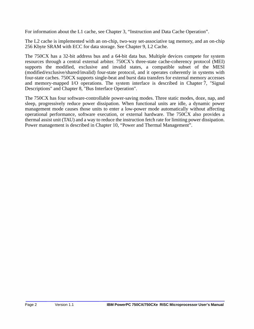
For information about the L1 cache, see Chapter 3, “Instruction and Data Cache Operation”.
The L2 cache is implemented with an on-chip, two-way set-associative tag memory, and an on-chip256 Kbyte SRAM with ECC for data storage. See Chapter 9, L2 Cache.
The 750CX has a 32-bit address bus and a 64-bit data bus. Multiple devices compete for systemresources through a central external arbiter. 750CX’s three-state cache-coherency protocol (MEI)supports the modified, exclusive and invalid states, a compatible subset of the MESI(modified/exclusive/shared/invalid) four-state protocol, and it operates coherently in systems withfour-state caches. 750CX supports single-beat and burst data transfers for external memory accessesand memory-mapped I/O operations. The system interface is described in Chapter 7, "SignalDescriptions" and Chapter 8, "Bus Interface Operation".
The 750CX has four software-controllable power-saving modes. Three static modes, doze, nap, andsleep, progressively reduce power dissipation. When functional units are idle, a dynamic powermanagement mode causes those units to enter a low-power mode automatically without affectingoperational performance, software execution, or external hardware. The 750CX also provides athermal assist unit (TAU) and a way to reduce the instruction fetch rate for limiting power dissipation.Power management is described in Chapter 10, “Power and Thermal Management”.
Page 2 Version 1.1 IBM PowerPC 750CX/750CXe RISC Microprocessor User’s Manual

Preliminary
Fig
ure
1-1.
750
CX
Mic
rop
roce
sso
r B
lock
Dia
gra
m
Add
ition
al F
eatu
res
• T
ime
Bas
e C
ount
er/D
ec-
rem
ente
r
• C
lock
Mul
tiplie
r
• JT
AG
/CO
P In
terf
ace
+
+
Fetc
her
Bran
ch P
roce
ssin
g
BTIC
64 E
ntry
+ x
÷F
PS
CR
CR
FPSC
R
CTR LR
BHT
Data
MM
U
Inst
ruct
ion
MM
U
PAEA
+ x
÷
Inst
ruct
ion
Unit
Unit
Inst
ruct
ion
Que
ue(6
Wor
d)
2 In
stru
ctio
ns
Res
erva
tion
Stat
ion
Res
erva
tion
Stat
ion
Res
erva
tion
Stat
ion
Inte
ger U
nit 1
Syst
em R
egis
ter
Unit
Dis
patc
h U
nit
64-B
it(2
Inst
ruct
ions
)
SRs
ITLB
(Sha
dow
)IB
ATAr
ray
32-K
byte
I Cac
heTa
gs
128-
Bit
(4 In
stru
ctio
ns)
32-B
it
Floa
ting-
Poin
tUn
it
Ren
ame
Buffe
rs(6
)
FPR
File
32-B
it
64-B
it
Res
erva
tion
Stat
ion
(2 E
ntry
)
Load
/Sto
re U
nit
(EA
Cal
cula
tion)
Stor
e Q
ueue
GPR
File
Ren
ame
Buffe
rs(6
)
32-B
it
SRs
(Orig
inal
)
DTL
B
DBA
TAr
ray
64-B
itCo
mpl
etio
n Un
it
Reo
rder
Buf
fer
(6 E
ntry
)
60x
Bus
Inte
rface
Uni
tIn
stru
ctio
n Fe
tch
Que
ue
L1 C
asto
ut Q
ueue
Dat
a Lo
ad Q
ueue
L2 C
ache
32-B
it Ad
dres
s Bu
s64
-Bit
Dat
a Bu
s
Inte
ger U
nit 2
L2C
R
256K
byte
SR
AM
Tags
32-K
byte
D C
ache
Rese
rvat
ion
Stat
ion
L2 T
ag
(2 E
ntry
)
64-B
it
256-
Bit
64-B
it
Pa
ge 3 V ersion 1.1 IBM PowerPC 750CX/750CXe RISC Microprocessor User’s Manual
1.2 750CX Microprocessor FeaturesThis section lists features of 750CX. The interrelationship of these features is shown in Figure 1-1 onpage 3.
1.2.1 Overview of 750CX Microprocessor FeaturesMajor features of 750CX are as follows.
• High-performance, superscalar microprocessor.
— As many as four instructions can be fetched from the instruction cache per clock cycle.
— As many as two instructions can be dispatched per clock.
— As many as six instructions can execute per clock (including two integer instructions).
— Single-clock-cycle execution for most instructions.
• Six independent execution units and two register files.
— BPU featuring both static and dynamic branch prediction.
– 64-entry (16-set, four-way set-associative) branch target instruction cache (BTIC), a cache of branch instructions that have been encountered in branch/loop code sequences. If a target instruction is in the BTIC, it is fetched into the instruction queue a cycle sooner than it can be made available from the instruction cache. Typically, if a fetch access hits the BTIC, it provides the first two instructions in the target stream effectively yielding a zero cycle branch.
– 512-entry branch history table (BHT) with two bits per entry for four levels of prediction—not-taken, strongly not-taken, taken, strongly taken.
– Branch instructions that do not update the count register (CTR) or link register (LR) are removed from the instruction stream.
— Two integer units (IUs) that share thirty-two GPRs for integer operands.
– IU1 can execute any integer instruction.
– IU2 can execute all integer instructions except multiply and divide instructions (multiply, divide, shift, rotate, arithmetic, and logical instructions). Most instructions that execute in the IU2 take one cycle to execute. The IU2 has a single-entry reservation station.
— Three-stage FPU.
– Fully IEEE 754-1985-compliant FPU for both single- and double-precision operations.
– Supports non-IEEE mode for time-critical operations.
– Hardware support for denormalized numbers.
– Two-entry reservation station.
– Thirty-two 64-bit FPRs for single or double-precision operands.
— Two-stage LSU.
– Two-entry reservation station.
– Single-cycle, pipelined cache access.
– Dedicated adder performs EA calculations.
Page 4 Version 1.1 IBM PowerPC 750CX/750CXe RISC Microprocessor User’s Manual

– Performs alignment and precision conversion for floating-point data.
– Performs alignment and sign extension for integer data.
– Three-entry store queue.
– Supports both big and little-endian modes.
— SRU handles miscellaneous instructions.
– Executes CR logical and Move to/Move from SPR instructions (mtspr and mfspr).
– Single-entry reservation station.
• Rename buffers.
– Six GPR rename buffers.
– Six FPR rename buffers.
– Condition register buffering supports two CR writes per clock.
• Completion unit.
— The completion unit retires an instruction from the six-entry reorder buffer (completion queue) when all instructions ahead of it have been completed, the instruction has finished execution, and no exceptions are pending.
— Guarantees sequential programming model and a precise exception model.
— Monitors all dispatched instructions and retires them in order.
— Tracks unresolved branches and flushes instructions from the mispredicted branch path.
— Retires as many as two instructions per clock.
• Separate on-chip L1 instruction and data caches (Harvard architecture).
— 32-Kbyte, eight-way set-associative instruction and data caches.
— Pseudo least-recently-used (PLRU) replacement algorithm.
— 32-byte (eight-word) cache block.
— Physically indexed/physical tags. (Note that the PowerPC architecture refers to physical address space as real address space.)
— Cache write-back or write-through operation programmable on a virtual-page or BAT-block basis.
— Instruction cache can provide four instructions per clock; data cache can provide two words per clock
— Caches can be disabled in software.
— Caches can be locked in software.
— Data cache coherency (MEI) maintained in hardware.
— The critical double word is made available to the requesting unit when it is read into the line-fill buffer. The cache is nonblocking, so it can be accessed during block reload.
• On-chip 1:1 L2 cache.
— 256 Kbyte on-chip ECC SRAMs.
— On-chip 2-way set-associative tag memory.
Table of Contents 5/9/02 Page 5

— ECC error correction for most single bit errors, detection of double bit errors
• Separate memory management units (MMUs) for instructions and data.
— 52-bit virtual address; 32-bit physical address.
— Address translation for virtual pages or variable-sized BAT blocks.
— Memory programmable as write-back/write-through, cacheable/noncacheable, and coherency enforced/coherency not enforced on a virtual page or BAT block basis.
— Separate IBATs and DBATs (four each) arrays for instructions and data, respectively.
— Separate virtual instruction and data translation lookaside buffers (TLBs).
– Both TLBs are 128-entry, two-way set associative, and use LRU replacement algorithm.
– TLBs are hardware-reloadable (the page table search is performed by hardware).
• Bus interface features include the following.
– Selectable bus-to-core clock frequency ratios of 2x, 2.5x, 3x, 3.5x, 4x, 4.5x ... 8x and 10x. (2x to 8x, all half-clock multipliers in-between).
– A 64-bit, split-transaction external data bus with burst transfers.
– Support for address pipelining and limited out-of-order bus transactions.
– Eight word reload buffer for L1 data cache.
– Single-entry instruction fetch queue.
– Two-entry L2 cache castout queue.
– No-DRTRY mode eliminates the DRTRY signal from the qualified bus grant. This allows the forwarding of data during load operations to the internal core one bus cycle sooner than if the use of DRTRY is enabled.
• Multiprocessing support features include the following:
— Hardware-enforced, three-state cache coherency protocol (MEI) for data cache.
— Load/store with reservation instruction pair for atomic memory references, semaphores, and other multiprocessor operations
• Power and thermal management
— Three static modes, doze, nap, and sleep, progressively reduce power dissipation:
– Doze—All the functional units are disabled except for the time base/decrementer registers and the bus snooping logic.
– Nap—The nap mode further reduces power consumption by disabling bus snooping, leaving only the time base register and the PLL in a powered state.
– Sleep—All internal functional units are disabled, after which external system logic may disable the PLL and SYSCLK.
— Thermal management facility provides software-controllable thermal management. Thermal management is performed through the use of three supervisor-level registers and an 750CX-specific thermal management exception.
— Instruction cache throttling provides control to slow instruction fetching to limit power consumption.
Page 6 Version 1.1 IBM PowerPC 750CX/750CXe RISC Microprocessor User’s Manual

• Performance monitor can be used to help debug system designs and improve software efficiency.
• In-system testability and debugging features through JTAG boundary-scan capability.
1.2.2 Instruction FlowAs shown in Figure 1-1 on page 3, the 750CX instruction unit provides centralized control ofinstruction flow to the execution units. The instruction unit contains a sequential fetcher, six-entryinstruction queue (IQ), dispatch unit, and BPU. It determines the address of the next instruction to befetched based on information from the sequential fetcher and from the BPU.
See Chapter 6, “Instruction Timing” for more information.
The sequential fetcher loads instructions from the instruction cache into the instruction queue. TheBPU extracts branch instructions from the sequential fetcher. Branch instructions that cannot beresolved immediately are predicted using either 750CX-specific dynamic branch prediction or thearchitecture-defined static branch prediction.
Branch instructions that do not update the LR or CTR are removed from (folded out) the instructionstream. Instruction fetching continues along the predicted path of the branch instruction.
Instructions issued to execution units beyond a predicted branch can be executed but are not retireduntil the branch is resolved. If branch prediction is incorrect, the completion unit flushes allinstructions fetched on the predicted path, and instruction fetching resumes along the correct path.
1.2.2.1 Instruction Queue and Dispatch UnitThe instruction queue (IQ), shown in Figure 1-1 on page 3, holds as many as six instructions and loadsup to four instructions from the instruction cache during a single processor clock cycle. Theinstruction fetcher continuously attempts to load as many instructions as there were vacancies createdin the IQ in the previous clock cycle. All instructions except branches are dispatched to theirrespective execution units from the bottom two positions in the instruction queue (IQ0 and IQ1) at amaximum rate of two instructions per cycle. Reservation stations are provided for the IU1, IU2, FPU,LSU, and SRU for dispatched instructions. The dispatch unit checks for source and destinationregister dependencies, allocates rename buffers, determines whether a position is available in thecompletion queue, and inhibits subsequent instruction dispatching if these resources are not available.
Branch instructions can be detected, decoded, and predicted from anywhere in the instruction queue.For a more detailed discussion of instruction dispatch, see Section 6.6.1 this manual.
1.2.2.2 Branch Processing Unit (BPU)The BPU receives branch instructions from the sequential fetcher and performs CR lookaheadoperations on conditional branches to resolve them early, achieving the effect of a zero-cycle branchin many cases.
Unconditional branch instructions and conditional branch instructions in which the condition isknown can be resolved immediately. For unresolved conditional branch instructions, the branch pathis predicted using either the architecture-defined static branch prediction or 750CX-specific dynamicbranch prediction. Dynamic branch prediction is enabled if HID0[BHT] = 1.
Table of Contents 5/9/02 Page 7

When a prediction is made, instruction fetching, dispatching, and execution continue along thepredicted path, but instructions can not be retired and write results back to architected registers untilthe prediction is determined to be correct (resolved). When a prediction is incorrect, the instructionsfrom the incorrect path are flushed from the processor and instruction fetching resumes along thecorrect path. 750CX allows a second branch instruction to be predicted; instructions from the secondpredicted branch instruction stream can be fetched but cannot be dispatched. These instructions areheld in the instruction queue.
Dynamic prediction is implemented using a 512-entry branch history table (BHT), a cache thatprovides two bits per entry that together indicate four levels of prediction for a branchinstruction—not-taken, strongly not-taken, taken, strongly taken. When dynamic branch prediction isdisabled, the BPU uses a bit in the instruction encoding to predict the direction of the conditionalbranch. Therefore, when an unresolved conditional branch instruction is encountered, 750CXexecutes instructions from the predicted path although the results are not committed to architectedregisters until the conditional branch is resolved. This execution can continue until a secondunresolved branch instruction is encountered.
When a branch is taken (or predicted as taken), the instructions from the untaken path must be flushedand the target instruction stream must be fetched into the IQ. The BTIC is a 64-entry cache thatcontains the most recently used branch target instructions, typically in pairs. When an instructionfetch hits in the BTIC, the instructions arrive in the instruction queue in the next clock cycle, a clockcycle sooner than they would arrive from the instruction cache. Additional instructions arrive fromthe instruction cache in the next clock cycle. The BTIC reduces the number of missed opportunitiesto dispatch instructions and gives the processor a one-cycle head start on processing the target stream.With the use of the BTIC the 750CX achieves a zero cycle delay for branches taken. Coherency ofthe BTIC table is maintained by table reset on an icache flush invalidate, icbi or rfi instructionexecution or when an exception is taken.
The BPU contains an adder to compute branch target addresses and three user-control registers—thelink register (LR), the count register (CTR), and the CR. The BPU calculates the return pointer forsubroutine calls and saves it into the LR for certain types of branch instructions. The LR also containsthe branch target address for the Branch Conditional to Link Register (bclrx) instruction. The CTRcontains the branch target address for the Branch Conditional to Count Register (bcctrx) instruction.Because the LR and CTR are SPRs, their contents can be copied to or from any GPR. Because theBPU uses dedicated registers rather than GPRs or FPRs, execution of branch instructions is largelyindependent from execution of integer and floating-point instructions.
1.2.2.3 Completion UnitThe completion unit operates closely with the dispatch unit. Instructions are fetched and dispatchedin program order. At the point of dispatch, the program order is maintained by assigning eachdispatched instruction a successive entry in the six-entry completion queue. The completion unittracks instructions from dispatch through execution and retires them in program order from the twobottom entries in the completion queue (CQ0 and CQ1).
Instructions cannot be dispatched to an execution unit unless there is a vacancy in the completionqueue and rename buffers are available. Branch instructions that do not update the CTR or LR areremoved from the instruction stream and do not occupy a space in the completion queue. Instructionsthat update the CTR and LR follow the same dispatch and completion procedures as non-branchinstructions, except that they are not issued to an execution unit.
Page 8 Version 1.1 IBM PowerPC 750CX/750CXe RISC Microprocessor User’s Manual

An instruction is retired when it is removed from the completion queue and it’s results are written toarchitected registers (GPRs, FPRs, LR, and CTR) from the rename buffers. In-order completionensures program integrity and the correct architectural state when 750CX must recover from amispredicted branch or any exception. Also, the rename buffer(s) assigned to it by the dispatch unitare returned to the available rename buffer pool. These rename buffers are reused by the dispatch unitfor subsequent instructions being dispatched.
For a more detailed discussion of instruction completion, see Section 6.6.1 in this manual.
1.2.2.3.1 Independent Execution UnitsIn addition to the BPU, 750CX has the following five execution units.
• Two Integer Units (IUs)
• Floating-Point Unit (FPU)
• Load/Store Unit (LSU)
• System Register Unit (SRU)
Each is described in the following sections.
1.2.2.3.2 Integer Units (IUs)The integer units IU1 and IU2 are shown in Figure 1-1 on page 3. The IU1 can execute any integerinstruction; the IU2 can execute any integer instruction except multiplication and divisioninstructions. Each IU has a single-entry reservation station that can receive instructions from thedispatch unit and operands from the GPRs or the rename buffers. The output of the IU is latched inthe rename buffer assigned to the instruction by the dispatch unit.
Each IU consists of three single-cycle subunits—a fast adder/comparator, a subunit for logicaloperations, and a subunit for performing rotates, shifts, and count-leading-zero operations. Thesesubunits handle all one-cycle arithmetic and logical integer instructions; only one subunit can executean instruction at a time.
The IU1 has a 32-bit integer multiplier/divider as well as the adder, shift, and logical units of the IU2.The multiplier supports early exit for operations that do not require full 32 x 32-bit multiplication.Multiply and divide instructions spend several cycles in the execution stage before the results arewritten to the output rename buffer.
1.2.2.3.3 Floating-Point Unit (FPU)The FPU, shown in Figure 1-1 on page 3, is designed as a three stage pipelined processing unit, wherethe first stage is for multiply, the second stage is for add and the third stage is for normalize. Asingle-precision multiply-add operation is processed with one cycle through put and three cyclelatency. (a single-precision instruction spends one cycle in each stage of the FPU). A double-precisionmultiply requires two cycles in the multiply stage and one cycle in each additional stage. Adouble-precision multiply-add has a two cycle through put and a four cycle latency. As instructionsare dispatched to the FPU’s reservation station, source operand data can be accessed from the FPRsor from the FPR rename buffers. Results in turn are written to the rename buffers and are madeavailable to subsequent instructions. Instructions pass through the reservation station and the pipe linestages in program order. Stalls due to contention for FPRs are minimized by automatic allocation ofthe six floating-point rename buffers. The completion unit writes the contents of the rename buffer tothe appropriate FPR when floating-point instructions are retired.
Table of Contents 5/9/02 Page 9

The 750CX supports all IEEE 754 floating-point data types (normalized, denormalized, NaN, zero,and infinity) in hardware, eliminating the latency incurred by software exception routines. (Note that“exception” is also referred to as “interrupt” in the architecture specification.)
1.2.2.3.4 Load/Store Unit (LSU)The LSU executes all load and store instructions and provides the data transfer interface between theGPRs, FPRs, and the data cache/memory subsystem. The LSU functions as a two stage pipe-linedunit where it calculates effective addresses in the first stage. In second stage the address is translated,the cache is accessed and the data is aligned if necessary. Unless extensive data alignment is required(e.g. crossing double word boundary) the instructions complete in two cycles with a one cycle throughput. The LSU also provides sequencing for load/store string and multiple register transferinstructions.
Load and store instructions are translated and issued in program order; however, some memoryaccesses can occur out of order. Synchronizing instructions can be used to enforce strict ordering ifnecessary. When there are no data dependencies and the guard bit for the page or block is cleared, amaximum of one out-of-order cacheable load operation can execute per cycle, with a two-cycle totallatency on a cache hit. Data returned from the cache is held in a rename buffer until the completionlogic commits the value to a GPR or FPR. Stores cannot be executed out of order and are held in thestore queue until the completion logic signals that the store operation is to be completed to memory.750CX executes store instructions with a maximum throughput of one per cycle and a three-cyclelatency to the data cache. The time required to perform the actual load or store operation depends onthe processor/bus clock ratio and whether the operation involves the L1 cache, the L2 cache, systemmemory, or an I/O device.
1.2.2.3.5 System Register Unit (SRU)The SRU executes various system-level instructions, as well as condition register logical operationsand move to/from special-purpose register instructions. To maintain system state, most instructionsexecuted by the SRU are execution-serialized with other instructions; that is, the instruction is heldfor execution in the SRU until all previously issued instructions have been retired. Results fromexecution-serialized instructions executed by the SRU are not available or forwarded for subsequentinstructions until the instruction completes.
1.2.3 Memory Management Units (MMUs)The 750CX’s MMUs support up to 4 Petabytes (252) of virtual memory and 4 Gigabytes (232) ofphysical memory for instructions and data. The MMUs also control access privileges for these spaceson block and page granularities. Referenced and changed status is maintained by the processor foreach page to support demand-paged virtual memory systems.
The LSU with the aid of the MMU translates effective addresses for data loads and stores; theeffective address is calculated on the first cycle and the MMU translates it to a physical address at thesame time it is accessing the L1 cache on the second cycle. The MMU also provides the necessarycontrol and protection information to complete the access. By the end of the second cycle the data andcontrol information is available if no miss conditions for translate and cache access were encountered.This yields a one cycle through put and a two cycle latency.
The 750CX supports the following types of memory translation.
Page 10 Version 1.1 IBM PowerPC 750CX/750CXe RISC Microprocessor User’s Manual

• Real addressing mode—In this mode, translation is disabled (control bits MSR(IR)=0 for instructions and MSR(DR)=0 for data) and the effective address is used as the physical address to access memory.
• Virtual page address translation—translates from an effective address to a physical address by using the segment registers and the TLB and access data from a 4-Kbyte virtual page. This page is either in physical memory or on disk. If the latter a page-fault exception occurs.
• Block address translation—translates the effective address into a physical address by using the BAT registers and accesses a block (128Kbytes to 256Mbytes) in memory.
If translation is enabled, the appropriate MMU translates the higher-order bits of the effective addressinto physical address bits by either BATs or page translation method. The lower-order address bits(that are untranslated and therefore, considered both logical and physical) are directed to the L1caches where they form the index into the eight-way set-associative tag and data arrays. Aftertranslating the address, the MMU passes the higher-order physical address bits to the cache and thecache lookup completes. For caching-inhibited accesses or accesses that miss in the cache, theuntranslated lower-order address bits are concatenated with the translated higher-order address bits;the resulting 32-bit physical address is used accesses the L2 cache or system memory via the 60x bus.
If the BAT registers are enabled and the address translates via this method, the page translation iscanceled and the high-order physical address bits from the BAT register are forward to thecache/memory access system. There are four 8-byte BAT registers which function like an associativememory. These registers provide cache control and protection information as well as addresstranslation. Only one of the 4 BAT entries should translate a given effective address.
If address relocation is enabled and the effective address doesn’t translate via the BAT method, virtualpage method is used. The 4 high-order bits of the effective address are used to access the 16 entrysegment register array. From this array a 24-bit segment register is accessed and used to form thehigh-order bits of a 52-bit virtual address. The low-order 28-bits of the effective address are used toform the low-order bits of the virtual address. This 52-bit virtual address is translated into a physicaladdress by doing a lookup in the TLB. If the lookup is successful a physical address is formed byusing 16 low-order bits from the virtual address and 16 high-order bits from the TLB. The TLB alsoprovides cache control and protection information to be used by the cache/memory system.
TLBs are 128-entry, two-way set-associative caches that contain information about recentlytranslated virtual addresses. When an address translation is not in a TLB, the 750CX automaticallygenerates a page table search in memory to update the TLB. This search could find the desired entryin the L1 or L2 cache or in the page table in memory. The time to reload a TLB entry depends onwhere it is found and could be completed in just several cycles. If memory is search a maximum of16 bus cycles would be needed before a page fault exception is signaled.
1.2.4 On-Chip Level 1 Instruction and Data CachesThe 750CX implements separate instruction and data caches. Each cache is 32-Kbyte and eight-wayset associative. As defined by the PowerPC architecture, they are physically indexed. Each cacheblock contains eight contiguous words from memory that are loaded from an 8-word boundary (thatis, bits EA[27–31] are zeros); thus, a cache block never crosses a page boundary. A miss in the L1cache causes a block reload from either the L2 if the block is in the L2 or from main memory. Thecritical double word is accessed first and forwarded to the load/store unit and written into an 8 wordbuffer. Subsequent double words are fetch from either the L2 or the system memory and written intothe buffer. Once the total block is in the buffer the line is written into the L1 cache in a single cycle
Table of Contents 5/9/02 Page 11

via a 256 buffer-to-L1 bus. This minimizes write cycles into the L1 leaving more read/write cyclesavailable to the LSU. The L1 is non-blocking and supports hits under misses during this reload.Misaligned accesses across a block or page boundary can incur a performance penalty.
The 750CX L1 cache organization is shown in Figure 1-2 on page 12.
Figure 1-2. Cache Organization
The data cache provides double-word accesses to the LSU each cycle. Like the instruction cache, thedata cache can be invalidated all at once or on a per-cache-block basis. The data cache can be disabledand invalidated by clearing HID0[DCE] and setting HID0[DCFI]. The data cache can be locked bysetting HID0[DLOCK]. To ensure cache coherency, the data cache supports the three-state MEIprotocol. The data cache tags are single-ported, so a simultaneous load or store and a snoop accessrepresent a resource collision and a LSU access is delayed for one cycle. If a snoop hit occurs and acast-out is required, the LSU is blocked internally for one cycle to allow the eight-word block of datato be copied to the write-back buffer.
The data bus width for bus interface unit (BIU) accesses of the L1 data cache array is 64 bits on the750 and cast out or reload of a 32-byte cache line requires four access cycles. On the 750CX, this bushas been expanded to 256 bits with access to an intermediate 32-byte buffer. As a result, cache blockscan be read from or written to the cache array in a single cycle, reducing cache contention betweenthe BIU, the L1 and the load-store unit. See Figure 9-1. on Page 9-2.
The instruction cache provides up to four instructions to the instruction queue in a single cycle. Theinstruction cache can be invalidated entirely or on a cache-block basis. The instruction cache can bedisabled and invalidated by clearing HID0[ICE] and setting HID0[ICFI]. The instruction cache can
8 Words/Way
128 Sets
Way 5
Way 6
Way 7
Way 4 Address Tag 4
Address Tag 5
Address Tag 6
Address Tag 7
Way 1
Way 2
Way 3
Way 0 Address Tag 0
Address Tag 1
Address Tag 2
Address Tag 3
State
State
State
Words [0–7]
State
Words [0–7]
Words [0–7]
Words [0–7]
State
State
State
Words [0–7]
State
Words [0–7]
Words [0–7]
Words [0–7]
Page 12 Version 1.1 IBM PowerPC 750CX/750CXe RISC Microprocessor User’s Manual

be locked by setting HID0[ILOCK]. The instruction cache supports only the valid/invalid states andrequires software to maintain coherency if the underlying program changes.
750CX also implements a 64-entry (16-set, four-way set-associative) branch target instruction cache(BTIC). The BTIC is a cache of branch instructions that have been encountered in branch/loop codesequences. If the target instruction is in the BTIC, it is fetched into the instruction queue a cyclesooner than it can be made available from the instruction cache. Typically the BTIC contains the firsttwo instructions in the target stream. The BTIC can be disabled and invalidated through software.
Coherency of the BTIC is transparent to the running software and is coupled with various functionsin the750CX processor. When the BTIC is enabled and loaded with instruction pairs to support zerocycle delay on branches taken, the table must be invalidated if the underlying program changes. (Thisis also true for the I-cache.) The BTIC is reset on an icache flush invalidate, an icbi or rfi instruction,and any exception.
For more information and timing examples showing cache hit and cache miss latencies, see Section6.3.2, “Instruction Fetch Timings” in this manual.
1.2.5 On-Chip Level 2 Cache Implementation The L2 cache is a unified cache that receives memory requests from both the L1 instruction and datacaches independently. The L2 cache is implemented with a L2 cache control register (L2CR), anon-chip, two-way, set-associative tag array, and with a 256-Kbyte, on-chip SRAM for data storage.The L2 cache normally operates in write-back mode and supports cache coherency through snooping.The access interface to the L2 is 64 bits and requires 4 cycles to read or write a single cache block.The L2 uses ECC on a double word and corrects most single bit errors and detects all double bit errors.See Figure 9.1 in Chapter 9, “L2 Cache”.
The L2 cache is organized with 64-byte lines, which in turn are subdivided into 32-byte blocks, theunit at which cache coherency is maintained. This reduces the size of the tag array and one tagsupports two cache blocks. Each 32-byte cache block has its own valid and modified status bits. Whena cache line is removed, both blocks and the tag are removed from the L2 cache. The cache block isonly written to system memory if the modified bit is set.
Requests from the L1 cache generally result from instruction misses, data load or store misses,write-through operations, or cache management instructions. Misses from the L1 cache are looked upin the L2 tags and serviced by the L2 cache if they hit; they are forwarded to the 60x bus interface ifthey miss.
The L2 cache can accept multiple, simultaneous accesses, however, they are serialized and processedone per cycle. The L1 instruction cache can request an instruction at the same time that the L1 datacache is requesting one load and two store operations. The L2 cache also services snoop requests fromthe bus. If there are multiple pending requests to the L2 cache, snoop requests have highest priority.The next priority consists of load and store requests from the L1 data cache. The next priority consistsof instruction fetch requests from the L1 instruction cache.
1.2.6 System Interface/Bus Interface Unit (BIU)As described in the preface section, the PowerPC 750CX uses a reduced system signal set, whicheliminates some 60X Bus optional protocol pins. The system designer needs to make note of thesedifferences.
Table of Contents 5/9/02 Page 13

The address and data buses operate independently; address and data tenures of a memory access aredecoupled to provide a more flexible control of bus traffic. The primary activity of the systeminterface is transferring data and instructions between the processor and system memory. There aretwo types of memory accesses:
• Single-beat transfers—These memory accesses allow transfer sizes of 8, 16, 24, 32, or 64 bits in one bus clock cycle. Single-beat transactions are caused by uncacheable read and write operations that access memory directly when caches are disabled, for cache-inhibited accesses, and for stores in write-through mode. The two latter accesses are defined by control bits provided by the MMU during address translation.
• Four-beat burst (32 byte) data transfers—Burst transactions, which always transfer an entire cache block (32 bytes), are initiated when an entire cache block is transferred. If the caches on 750CX are enabled and using write-back mode, burst-read operations are the most common memory accesses, followed by burst-write memory operations.
The 750CX also supports address-only operations, variants of the burst and single-beat operations,(for example, atomic memory operations and global memory operations that are snooped), andaddress retry activity (for example, when a snooped read access hits a modified block in the cache).The broadcast of some address-only operations is controlled through HID0[ABE]. I/O accesses usethe same protocol as memory accesses.
Access to the system interface is granted through an external arbitration mechanism that allowsdevices to compete for bus mastership. This arbitration mechanism is flexible, allowing 750CX to beintegrated into systems that implement various fairness and bus parking procedures to avoidarbitration overhead.
Typically, memory accesses are weakly ordered—sequences of operations, including load/store stringand multiple instructions, do not necessarily complete in the order they begin—maximizing theefficiency of the bus without sacrificing data coherency. 750CX allows read operations to go aheadof store operations (except when a dependency exists, or in cases where a noncacheable access isperformed), and provides support for a write operation to go ahead of a previously queued read datatenure (for example, letting a snoop push be enveloped between address and data tenures of a readoperation). Because 750CX can dynamically optimize run-time ordering of load/store traffic, overallperformance is improved.
The system interface is specific for each PowerPC microprocessor implementation.
The 750CX signals are grouped as shown in Figure 1-3. Test and control signals provide diagnosticsfor selected internal circuits.
Page 14 Version 1.1 IBM PowerPC 750CX/750CXe RISC Microprocessor User’s Manual
Figure 1-3. System Interface
The system interface supports address pipelining, which allows the address tenure of one transactionto overlap the data tenure of another. The extent of the pipelining depends on external arbitration andcontrol circuitry. Similarly, the 750CX supports split-bus transactions for systems with multiplepotential bus masters—one device can have mastership of the address bus while another hasmastership of the data bus. Allowing multiple bus transactions to occur simultaneously increases theavailable bus bandwidth for other activity.
The 750CX’s clocking structure supports a wide range of processor-to-bus clock ratios.
1.2.7 SignalsThe 750CX’s signals are grouped as follows.
• Address arbitration signals—The 750CX uses these signals to arbitrate for address bus mastership.
• Address start signals—These signals indicate that a bus master has begun a transaction on the address bus.
• Address transfer signals—These signals include the address bus and are used to transfer the address.
• Transfer attribute signals—These signals provide information about the type of transfer, such as the transfer size and whether the transaction is bursted, write-through, or caching-inhibited.
• Address termination signals—These signals are used to acknowledge the end of the address phase of the transaction. They also indicate whether a condition exists that requires the address phase to be repeated.
• Data arbitration signals—The 750CX uses these signals to arbitrate for data bus mastership.
• Data transfer signals—These signals include the data bus and are used to transfer the data.
• Data termination signals—Data termination signals are required after each data beat in a data transfer. In a single-beat transaction, a data termination signal also indicates the end of the tenure; in burst accesses, data termination signals apply to individual beats and indicate the end of the tenure only after the final data beat.
Address Arbitration
Address Start
Address Transfer
Transfer Attribute
Address Termination Clocks
Data Arbitration
Data Transfer
Data Termination
Processor Status/Control
Test and Control
System Status
VDD VDD (I/O)
750CX
Table of Contents
5/9/02 Page 15
• Interrupt signals—These signals include the interrupt signal, checkstop signals, and both soft reset and hard reset signals. These signals are used to generate interrupt exceptions and, under various conditions, to reset the processor.
• Processor status/control signals—These signals are used to indicate miscellaneous bus functions.
• JTAG/COP interface signals—The common on-chip processor (COP) unit provides a serial interface to the system for performing board-level boundary scan interconnect tests.
• Clock signals—These signals determine the system clock frequency. These signals can also be used to synchronize multiprocessor systems.
NOTE: A bar over a signal name indicates that the signal is active low—for example, ARTRY (address retry) and TS (transfer start). Active-low signals are referred to as asserted (active) when they are low and negated when they are high. Signals that are not active low, such as A[0–31] (address bus signals) and TT[0–4] (transfer type signals) are referred to as asserted when they are high and negated when they are low.
Page 16 Version 1.1 IBM PowerPC 750CX/750CXe RISC Microprocessor User’s Manual

1.2.8 Signal ConfigurationFigure 1-4. shows 750CX’s logical pin configuration. The signals are grouped by function.
Figure 1-4. 750CX Microprocessor Signal Groups
Signal functionality is described in detail in Chapter 7 “Signal Descriptions” and Chapter 8, “BusInterface Operations”.
NOTE: The 750CX has a reduced set of signals from the PowerPC 750 PID8 series of microprocessors. The PowerPC 750CX Datasheet, should be referenced for the complete signal pins present on the PowerPC 750CX.
1.2.9 Clocking750CX requires a single system clock input, SYSCLK, that represents the bus interface frequency.Internally, the processor uses a phase-locked loop (PLL) circuit to generate a master core clock that
DataArbitration
BR
BG
TS
AP[0–3]
GBL
TSIZ[0–2]
AACK
ARTRY
SYSCLKDBG
D[0–63]
DP[0–7]
TA
DRTRY
TEA
INT
JTAG/COP
Factory Test
1
11
1
5
3
4
TBST
WT
PLL_CFG[0–3]
TT[0–4]5
4
1
MCP
SRESET
TLBISYNC
HRESET
QREQ
QACK
CKSTP_IN
CKSTP_OUT
1
3
1
1
1
1
1
8
64
1
1
1
1
1
1
1
1
1
1
CI 1
A[0–31]32
Address Arbitration
AddressBus
AddressTermination
AddressStart
TransferAttributes
DataTransfer
DataTermination
Interrupts/Resets
ProcessorStatus/Control
VDD VDD (I/O)
ClockControl
TestInterface
750CX
AVDD
Data Termination
Data Transfer
Processor/StatusControl
Address Bus
Note: Items in Italics are optional items
Table o
f Contents 5/9 /02 Page 17
is frequency-multiplied and phase-locked to the SYSCLK input. This core frequency is used tooperate the internal circuitry.
The PLL is configured by the PLL_CFG[0–3] signals, which select the multiplier that the PLL usesto multiply the SYSCLK frequency up to the internal core frequency. The feedback in the PLLguarantees that the processor clock is phase locked to the bus clock, regardless of process variations,temperature changes, or parasitic capacitances.
The PLL also ensures a 50% duty cycle for the processor clock.
750CX supports various processor-to-bus clock frequency ratios, although not all ratios are availablefor all frequencies. Configuration of the processor/bus clock ratios is displayed through a750CX-specific register, HID1. For information about supported clock frequencies, see the 750CXDatasheet.
1.3 750CX Microprocessor: ImplementationThe PowerPC architecture is derived from the POWER architecture (Performance Optimized WithEnhanced RISC architecture). The PowerPC architecture shares the benefits of the POWERarchitecture optimized for single-chip implementations. The PowerPC architecture design facilitatesparallel instruction execution and is scalable to take advantage of future technological gains.
This section describes the PowerPC architecture in general, and specific details about theimplementation of 750CX as a low-power, 32-bit member of the PowerPC processor family. Thestructure of this section follows the organization of the user’s manual; each subsection provides anoverview of each chapter.
• Registers and programming model—Section 1.4, ”PowerPC Registers and Programming Model,” on Page 1-20 describes the registers for the operating environment architecture common among PowerPC processors and describes the programming model. It also describes the registers that are unique to 750CX. The information in this section is described more fully in Chapter 2, "Programming Model".
• Instruction set and addressing modes—Section 1.5, ”Instruction Set,” on Page 1-24 describes the PowerPC instruction set and addressing modes for the PowerPC operating environment architecture, defines the PowerPC instructions implemented in 750CX, and describes new instruction set extensions to improve the performance of single-precision floating-point operations and the capability of data transfer. The information in this section is described more fully in Section 1, ”PowerPC 750CX Overview,” on Page 1-1.
• Cache implementation—Section 1.6, ”On-Chip Cache Implementation,” on Page 1-26 describes the cache model that is defined generally for PowerPC processors by the virtual environment architecture. It also provides specific details about 750CX L2 cache implementation.
• Exception model—Section 1.7, ”Exception Model,” on Page 1-27 describes the exception model of the PowerPC operating environment architecture and the differences in 750CX exception model. The information in this section is described more fully in Chapter 4, "Exceptions".
Page 18 Version 1.1 IBM PowerPC 750CX/750CXe RISC Microprocessor User’s Manual

• Memory management—Section 1.8, ”Memory Management,” on Page 1-30 describes generally the conventions for memory management among the PowerPC processors. This section also describes 750CX’s implementation of the 32-bit PowerPC memory management specification. The information in this section is described more fully in Chapter 5, "Memory Management".
• Instruction timing—Section 1.9, ”Instruction Timing,” on Page 1-31 provides a general description of the instruction timing provided by the superscalar, parallel execution supported by the PowerPC architecture and 750CX. The information in this section is described more fully in Chapter 6, "Instruction Timing".
• Power management—Section 1.10, ”Power Management,” on Page 1-33 describes how the power management can be used to reduce power consumption when the processor, or portions of it, are idle. The information in this section is described more fully in Chapter 10, "Power and Thermal Management".
• Thermal management—Section 1.11, ”Thermal Management,” on Page 1-34 describes how the thermal management unit and its associated registers (THRM1–THRM3) and exception can be used to manage system activity in a way that prevents exceeding system and junction temperature thresholds. This is particularly useful in high-performance portable systems, which cannot use the same cooling mechanisms (such as fans) that control overheating in desktop systems. The information in this section is described more fully in Chapter 10, "Power and Thermal Management".
• Performance monitor—Section 1.12, ”Performance Monitor,” on Page 1-35 describes the performance monitor facility, which system designers can use to help bring up, debug, and optimize software performance. The information in this section is described more fully in Chapter 11, "Performance Monitor".
The following sections summarize the features of 750CX, distinguishing those that are defined by thearchitecture from those that are unique to 750CX implementation.
The PowerPC architecture consists of the following layers, and adherence to the PowerPCarchitecture can be described in terms of which of the following levels of the architecture isimplemented.
• PowerPC user instruction set architecture (UISA)—Defines the base user-level instruction set, user-level registers, data types, floating-point exception model, memory models for a uniprocessor environment, and programming model for a uniprocessor environment.
• PowerPC virtual environment architecture (VEA)—Describes the memory model for a multiprocessor environment, defines cache control instructions, and describes other aspects of virtual environments. Implementations that conform to the VEA also adhere to the UISA, but may not necessarily adhere to the OEA.
• PowerPC operating environment architecture (OEA)—Defines the memory management model, supervisor-level registers, synchronization requirements, and the exception model. Implementations that conform to the OEA also adhere to the UISA and the VEA.
The PowerPC architecture allows a wide range of designs for such features as cache and systeminterface implementations. 750CX implementations support the three levels of the architecturedescribed above. For more information about the PowerPC architecture, see the PowerPCMicroprocessor Family: The Programming Environments manual.
Specific features of 750CX are listed in Section 1.2, ”750CX Microprocessor Features,” on Page 1-4.
Table of Contents 5/9/02 Page 19
1.4 PowerPC Registers and Programming ModelThe PowerPC architecture defines register-to-register operations for most computational instructions.Source operands for these instructions are accessed from the registers or are provided as immediatevalues embedded in the instruction itself. The three-register instruction formats allow specification ofa target register distinct from the two source operands. Only load and store instructions transfer databetween registers and memory.
PowerPC processors have two levels of privilege—supervisor mode of operation (typically used bythe operating system) and user mode of operation (used by the application software, it is also calledproblem state). The programming models incorporate 32 GPRs, 32 FPRs, special-purpose registers(SPRs), and several miscellaneous registers. Each PowerPC microprocessor also has its own uniqueset of hardware implementation-dependent (HID) registers.
While running in supervisor mode the operating system is able to execute all instructions and accessall registers defined in the PowerPC architecture. In this mode the operating system establishes alladdress translations and protection mechanisms, loads all processor state registers. and sets up allother control mechanisms defined on the PowerPC 750CX processor. While running in user mode(problem state) many of these registers and facilities are not accessible and any attempt to read orwrite these register results in a program exception.
Figure 1-5 on page 21 shows all the 750CX registers available at the user and supervisor level. Thenumbers to the right of the SPRs indicate the number that is used in the syntax of the instructionoperands to access the register.
For more information, see Chapter 2, "Programming Model".
Page 20 Version 1.1 IBM PowerPC 750CX/750CXe RISC Microprocessor User’s Manual
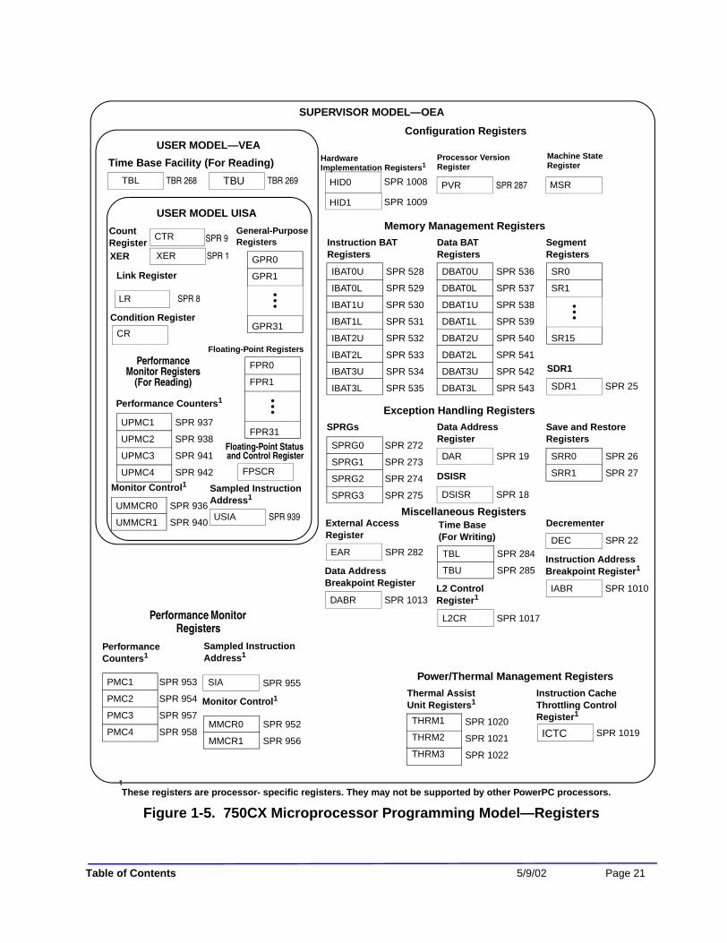
Figure 1-5. 750CX Microprocessor Programming Model—Registers
ICTC SPR 1019SPR 1020
SPR 1021
SPR 1022
SPR 937
SPR 938
SPR 941
SPR 942
PerformanceCounters1
Sampled InstructionAddress1
DSISR
Data AddressRegister
SPRGs
Exception Handling Registers
Save and Restore Registers
Instruction BATRegisters
Data BATRegisters
Memory Management Registers
Machine State Register
MSR
Processor VersionRegister
SPR 287PVR
Configuration Registers
Hardware Implementation Registers1
SPR 1
USER MODEL UISA
FPSCR
Condition Register
General-Purpose Registers
XER XER
SPR 8
Link Register
LR
SUPERVISOR MODEL—OEA
DecrementerExternal AccessRegister
EAR
SDR1
SPR 9Count Register
Miscellaneous Registers
SegmentRegisters
CR
Floating-Point Registers
Performance Monitor Registers
(For Reading)
Performance Counters1
Monitor Control1
SPR 939USIA
Sampled InstructionAddress1
Monitor Control1
Time Base(For Writing)
Power/Thermal Management Registers
Thermal AssistUnit Registers1
Instruction CacheThrottling ControlRegister1
USER MODEL—VEA
TBL TBR 268
Time Base Facility (For Reading)
CTR
GPR0
GPR1
GPR31
TBU TBR 269
IBAT0U
IBAT0L
IBAT1U
IBAT1L
IBAT2U
IBAT2L
IBAT3U
IBAT3L
SPR 528
SPR 529
SPR 530
SPR 531
SPR 532
SPR 533
SPR 534
SPR 535
SPR 536
SPR 537
SPR 538
SPR 539
SPR 540
SPR 541
SPR 542
SPR 543
DBAT0U
DBAT0L
DBAT1U
DBAT1L
DBAT2U
DBAT2L
DBAT3U
DBAT3L
SR0
SR1
SR15
SDR1 SPR 25
HID0
HID1
SPR 1008
SPR 1009
FPR0
FPR1
FPR31UPMC1
UPMC2
UPMC3
UPMC4
UMMCR0
UMMCR1
SPR 936
SPR 940
SPR 953
SPR 954
SPR 957
SPR 958
PMC1
PMC2
PMC3
PMC4
SIA SPR 955
MMCR0
MMCR1
SPR 952
SPR 956
SPRG0
SPRG1
SPRG2
SPRG3
SPR 272
SPR 273
SPR 274
SPR 275
DAR
DSISR
SPR 19
SPR 18
SRR0 SPR 26
SRR1 SPR 27
SPR 282 TBL SPR 284
TBU SPR 285
DEC SPR 22
Data AddressBreakpoint Register
DABR SPR 1013L2 ControlRegister1
L2CR SPR 1017
Instruction Address Breakpoint Register1
IABR SPR 1010
Floating-Point Statusand Control Register
These registers are processor- specific registers. They may not be supported by other PowerPC processors.1
Performance Monitor Registers
THRM1
THRM2
THRM3
Table of Contents 5/9
/02 Page 21
The following tables summarize the PowerPC registers implemented in 750CX; describe registers (excluding SPRs) defined by the architecture.
The OEA defines numerous special-purpose registers that serve a variety of functions, such asproviding controls, indicating status, configuring the processor, and performing special operations.During normal execution, a program can access the registers, shown in Figure 1-5 on page 21,depending on the program’s access privilege (supervisor or user, determined by the privilege-level(PR) bit in the MSR). GPRs and FPRs are accessed through operands that are defined in theinstructions. Access to registers can be explicit (that is, through the use of specific instructions for thatpurpose such as Move to Special-Purpose Register (mtspr) and Move from Special-Purpose Register(mfspr) instructions) or implicit, as the part of the execution of an instruction. Some registers can beaccessed both explicitly and implicitly.
In the 750CX, all SPRs are 32 bits wide. Table “Architecture-Defined SPRs Implemented,” describesthe architecture-defined SPRs implemented by 750CX. In the PowerPC Microprocessor Family: TheProgramming Environments manual, these registers are described in detail, including bit descriptions.Section 2.1.1 on Page 2-1 describes how these registers are implemented in the 750CX. In particular,this section describes which features the PowerPC architecture defines as optional and areimplemented on the 750CX.
Table 1-1 Architecture-Defined Registers (Excluding SPRs)
Register Level Function
CR User The condition register (CR) consists of eight four-bit fields that reflect the results of certain operations, such as move, integer and floating-point compare, arithmetic, and logical instructions, and provide a mechanism for testing and branching.
FPRs User The 32 floating-point registers (FPRs) serve as the data source or destination for floating-point instructions. These 64-bit registers can hold single- or double-precision floating-point values.
FPSCR User The floating-point status and control register (FPSCR) contains the floating-point exception signal bits, exception summary bits, exception enable bits, and rounding control bits needed for compliance with the IEEE-754 standard.
GPRs User The 32 GPRs contain the address and data arguments addressed from source or destination fields in integer instructions. Also floating-point load and store insturctions use GPRs for addressing memory.
MSR Supervisor The machine state register (MSR) defines the processor state. Its contents are saved when an exception is taken and restored when exception handling completes. 750CX implements MSR[POW], (defined by the architecture as optional), which is used to enable the power management feature. 750CX-specific MSR[PM] bit is used to mark a process for the performance monitor.
SR0–SR15 Supervisor The sixteen 32-bit segment registers (SRs) define the 4-Gbyte space as sixteen 256-Mbyte segments. 750CX implements segment registers as two arrays—a main array for data accesses and a shadow array for instruction accesses; see Figure 1-1 on page 3. Loading a segment entry with the Move to Segment Register (mtsr) instruction loads both arrays. The mfsr instruction reads the master register, shown as part of the data MMU in Figure 1-1 on page 3.
Page 22 Version 1.1 IBM PowerPC 750CX/750CXe RISC Microprocessor User’s Manual

Table “Implementation-Specific Registers,” describes the SPRs in 750CX that are not defined by thePowerPC architecture.
Section 2.1.2 on Page 2-8 gives detailed descriptions of these registers, including bit descriptions.
Table 1-2 Architecture-Defined SPRs Implemented
Register Level Function
LR User The link register (LR) can be used to provide the branch target address and to hold the return address after branch and link instructions.
BATs Supervisor The architecture defines 16 block address translation registers (BATs), which operate in pairs. There are four pairs of data BATs (DBATs) and four pairs of instruction BATs (IBATs). BATs are used to define and configure blocks of memory.
CTR User The count register (CTR) is decremented and tested by branch-and-count instructions.
DABR Supervisor The optional data address breakpoint register (DABR) supports the data address breakpoint facility.
DAR User The data address register (DAR) holds the address of an access after an alignment or DSI exception.
DEC Supervisor The decrementer register (DEC) is a 32-bit decrementing counter that provides a way to schedule time delayed exceptions.
DSISR User The DSISR defines the cause of data access and alignment exceptions.
EAR Supervisor The external access register (EAR) controls access to the external access facility through the External Control In Word Indexed (eciwx) and External Control Out Word Indexed (ecowx) instructions.
PVR Supervisor The processor version register (PVR) is a read-only register that identifies the processor version and revision level.
SDR1 Supervisor SDR1 specifies the page table address and size used in virtual-to-physical page address translation.
SRR0 Supervisor The machine status save/restore register 0 (SRR0) saves the address used for restarting an interrupted program when a Return from Interrupt (rfi) instruction executes (a.k.a. exceptions).
SRR1 Supervisor The machine status save/restore register 1 (SRR1) is used to save machine status on exceptions and to restore machine status when an rfi instruction is executed.
SPRG0–SPRG3 Supervisor SPRG0–SPRG3 are provided for operating system use.
TB User: readSupervisor:read/write
The time base register (TB) is a 64-bit register that maintains the time and date variable. The TB consists of two 32-bit fields—time base upper (TBU) and time base lower (TBL).
XER User The XER contains the summary overflow bit, integer carry bit, overflow bit, and a field specifying the number of bytes to be transferred by a Load String Word Indexed (lswx) or Store String Word Indexed (stswx) instruction.
Table of Contents 5/9/02 Page 23

.
1.5 Instruction SetAll PowerPC instructions are encoded as single-word (32-bit) instructions. Instruction formats areconsistent among all instruction types (primary op-code is always 6 bits, register operands alwaysspecified in the same bit fields in the instruction), permitting efficient decoding to occur in parallelwith operand accesses. This fixed instruction length and consistent format greatly simplify instructionpipelining.
For more information, see Chapter 2, "Programming Model".
Table 1-3 Implementation-Specific Registers
Register Level Function
HID0 Supervisor The hardware implementation-dependent register 0 (HID0) provides checkstop enables and other functions.
HID1 Supervisor The hardware implementation-dependent register 1 (HID1) allows software to read the configuration of the PLL configuration signals.
IABR Supervisor The instruction address breakpoint register (IABR) supports instruction address breakpoint exceptions. It can hold an address to compare with instruction addresses in the IQ. An address match causes an instruction address breakpoint exception.
ICTC Supervisor The instruction cache-throttling control register (ICTC) has bits for controlling the interval at which instructions are fetched into the instruction buffer in the instruction unit. This helps control 750CX’s overall junction temperature.
L2CR Supervisor The L2 cache control register (L2CR) is used to configure and operate the L2 cache.
MMCR0–MMCR1 Supervisor The monitor mode control registers (MMCR0–MMCR1) are used to enable various performance monitoring interrupt functions. UMMCR0–UMMCR1 provide user-level read access to MMCR0–MMCR1.
PMC1–PMC4 Supervisor The performance monitor counter registers (PMC1–PMC4) are used to count specified events. UPMC1–UPMC4 provide user-level read access to these registers.
SIA Supervisor The sampled instruction address register (SIA) holds the EA of an instruction executing at or around the time the processor signals the performance monitor interrupt condition. The USIA register provides user-level read access to the SIA.
THRM1, THRM2 Supervisor THRM1 and THRM2 provide a way to compare the junction temperature against two user-provided thresholds. The thermal assist unit (TAU) can be operated so that the thermal sensor output is compared to only one threshold, selected in THRM1 or THRM2.
THRM3 Supervisor THRM3 is used to enable the TAU and to control the output sample time.
UMMCR0–UMMCR1 User The user monitor mode control registers (UMMCR0–UMMCR1) provide user-level read access to MMCR0–MMCR1.
UPMC1–UPMC4 User The user performance monitor counter registers (UPMC1–UPMC4) provide user-level read access to PMC1–PMC4.
USIA User The user sampled instruction address register (USIA) provides user-level read access to the SIA register.
Page 24 Version 1.1 IBM PowerPC 750CX/750CXe RISC Microprocessor User’s Manual
1.5.1 PowerPC Instruction SetThe PowerPC instructions are divided into the following categories.
• Integer instructions—These include computational and logical instructions. — Integer arithmetic instructions
— Integer compare instructions
— Integer logical instructions
— Integer rotate and shift instructions
• Floating-point instructions—These include floating-point computational instructions, as well as instructions that affect the FPSCR.
— Floating-point arithmetic instructions
— Floating-point multiply/add instructions
— Floating-point rounding and conversion instructions
— Floating-point compare instructions
— Floating-point status and control instructions
• Load/store instructions—These include integer and floating-point load and store instructions.
— Integer load and store instructions
— Integer load and store multiple instructions
— Floating-point load and store
— Primitives used to construct atomic memory operations (lwarx and stwcx. instructions)
• Flow control instructions—These include branching instructions, condition register logical instructions, trap instructions, and other instructions that affect the instruction flow.
— Branch and trap instructions
— Condition register logical instructions (sets conditions for branches)
— System Call
• Processor control instructions—These instructions are used for synchronizing memory accesses and management of caches, TLBs, and the segment registers.
— Move to/from SPR instructions
— Move to/from MSR
— Synchronize (processor and memory system)
— Instruction synchronize
— Order loads and stores
• Memory control instructions—To provide control of caches, TLBs, and SRs.
— Supervisor-level cache management instructions
— User-level cache instructions
— Segment register manipulation instructions
— Translation lookaside buffer management instructions
Table of Contents 5/9/02 Page 25

This grouping does not indicate the execution unit that executes a particular instruction or group ofinstructions.
Integer instructions operate on byte, half-word, and word operands. Floating-point instructionsoperate on single-precision (one word) and double-precision (two words) floating-point operands.The PowerPC architecture uses instructions that are four bytes long and word-aligned. It provides forinteger byte, half-word, and word operand loads and stores between memory and a set of 32 GPRs. Italso provides for single and double-precision loads and stores between memory and a set of 32floating-point registers (FPRs).
Computational instructions do not access memory. To use a memory operand in a computation andthen modify the same or another memory location, the memory contents must be loaded into aregister, modified, and then written back to the target location using three or more instructions.
PowerPC processors follow the program flow when they are in the normal execution state; however,the flow of instructions can be interrupted directly by the execution of an instruction or by anasynchronous event. Either type of exception will cause the associated exception handler to beinvoked.
Effective address computations for both data and instruction accesses use 32-bit signed two’scomplement binary arithmetic. A carry from bit 0 and overflow are ignored.
1.5.2 750CX Microprocessor Instruction Set750CX instruction set is defined as follows.
• 750CX provides hardware support for all PowerPC instructions.
• 750CX implements the following instructions optional to the PowerPC architecture.
— External Control In Word Indexed (eciwx).
— External Control Out Word Indexed (ecowx).
— Floating Select (fsel).
— Floating Reciprocal Estimate Single-Precision (fres). *
— Floating Reciprocal Square Root Estimate (frsqrte). *
— Store Floating-Point as Integer Word (stfiw).* (fres and frsqrte have a resolution of <1/4000)
1.6 On-Chip Cache Implementation
The following subsections describe the PowerPC architecture’s treatment of cache in general, and 750CX-specific implementation, respectively. A detailed description of 750CX L1 cache implemen-tation is provided in Chapter 3, "The 750CX Instruction and Data Cache Operation".
1.6.1 PowerPC Cache Model
The PowerPC architecture does not define hardware aspects of cache implementations. For exam-ple, PowerPC processors can have unified caches, separate instruction and data caches (Harvard
Page 26 Version 1.1 IBM PowerPC 750CX/750CXe RISC Microprocessor User’s Manual

architecture), or no cache at all. PowerPC microprocessors control the following memory access modes on a virtual page or block (BAT) basis
• Write-back/write-through mode
• Caching-inhibited mode
• Memory coherency
The caches are physically addressed, and the data cache can operate in either write-back or write-through mode, as specified by the PowerPC architecture.
The PowerPC architecture defines the term ‘cache block’ as the cacheable unit. The VEA and OEA define cache management instructions that a programmer can use to affect cache contents.
1.6.2 750CX Microprocessor Cache Implementation
750CX cache implementation is described in Section 1.2.4, ”On-Chip Level 1 Instruction and Data Caches,” on Page 1-11 and Section 1.2.5, ”On-Chip Level 2 Cache Implementation,” on Page 1-13. The BPU also contains a 64-entry BTIC that provides immediate access to an instruction pair for taken branches. For more information, see Section 1.2.2.2, ”Branch Processing Unit (BPU),” on Page 1-7.
1.7 Exception Model
The following sections describe the PowerPC exception model and 750CX implementation. A detailed description of 750CX exception model is provided in Chapter 4, "Exceptions" in this man-ual.
1.7.1 PowerPC Exception Model
The PowerPC exception mechanism allows the processor to interrupt the instruction flow to handle certain situations caused by external signals, errors, or unusual conditions arising from the instruc-tion execution. When exceptions occur, information about the state of the processor is saved to cer-tain registers, and the processor begins execution at an address (exception vector) predetermined for each exception. System software must complete the saving of the processor state prior to servicing the exception. Exception processing proceeds in supervisor mode.
Although multiple exception conditions can map to a single exception vector, a more specificcondition may be determined by examining a register associated with the exception—for example,the MSR, DSISR and the FPSCR contain status bits which farther identify the exception condition.Additionally, some exception conditions can be explicitly enabled or disabled by software.
The PowerPC architecture requires that exceptions be handled in specific priority and program order;therefore, although a particular implementation may recognize exception conditions out of order, theyare handled in program order. When an instruction-caused exception is recognized, any unexecutedinstructions that appear earlier in the instruction stream, including any that are undispatched, arerequired to complete before the exception is taken, and any exceptions those instructions cause mustalso be handled first; likewise, asynchronous, precise exceptions are recognized when they occur but
Table of Contents 5/9/02 Page 27

are not handled until the instructions currently in the completion queue successfully retire or generatean exception, and the completion queue is emptied.
Unless a catastrophic condition causes a system reset or machine check exception, only one exceptionis handled at a time. For example, if one instruction encounters multiple exception conditions, thoseconditions are handled sequentially in priority order. After the exception handler completes, theinstruction processing continues until the next exception condition is encountered. Recognizing andhandling exception conditions sequentially guarantees system integrity.
When an exception is taken, information about the processor state before the exception was taken issaved in SRR0 and SRR1. Exception handlers must save the information stored in SRR0 and SRR1early to prevent the program state from being lost due to a system reset and machine check exceptionor due to an instruction-caused exception in the exception handler, and before re-enabling externalinterrupts. The exception handler must also save and restore any GPR registers used by the handler.
The PowerPC architecture supports four types of exceptions.
• Synchronous, precise—These are caused by instructions. All instruction-caused exceptions are handled precisely; that is, the machine state at the time the exception occurs is known and can be completely restored. This means that (excluding the trap and system call exceptions) the address of the faulting instruction is provided to the exception handler and that neither the faulting instruction nor subsequent instructions in the code stream will complete execution before the exception is taken. Once the exception is processed, execution resumes at the address of the faulting instruction (or at an alternate address provided by the exception handler). When an exception is taken due to a trap or system call instruction, execution resumes at an address provided by the handler.
• Synchronous, imprecise—The PowerPC architecture defines two imprecise floating-point exception modes, recoverable and nonrecoverable. Even though 750CX provides a means to enable the imprecise modes, it implements these modes identically to the precise mode (that is, enabled floating-point exceptions are always precise).
• Asynchronous, maskable—The PowerPC architecture defines external and decrementer interrupts as maskable, asynchronous exceptions. When these exceptions occur, their handling is postponed until the next instruction, and any exceptions associated with that instruction, completes execution. If no instructions are in the execution units, the exception is taken immediately upon determination of the correct restart address (for loading SRR0). As shown in the Table “750CX Microprocessor Exception Classifications,” the 750CX implements additional asynchronous, maskable exceptions.
• Asynchronous, nonmaskable—There are two nonmaskable asynchronous exceptions: system reset and the machine check exception. These exceptions may not be recoverable, or may provide a limited degree of recoverability. Exceptions report recoverability through the MSR[RI] bit.
1.7.2 750CX Microprocessor Exception ImplementationThe 750CX exception classes described above are shown in the Table “750CX MicroprocessorException Classifications.” Although exceptions have other characteristics, such as priority andrecoverability, Table 1-4 describes categories of exceptions 750CX handles uniquely. Table 1-4includes no synchronous imprecise exceptions; although the PowerPC architecture supportsimprecise handling of floating-point exceptions, 750CX implements these exception modes precisely.
Page 28 Version 1.1 IBM PowerPC 750CX/750CXe RISC Microprocessor User’s Manual

Table 1-5 lists the 750CX exceptions and conditions that cause them. Exceptions specific to 750CXare indicated.
Table 1-4 750CX Microprocessor Exception Classifications
Synchronous/Asynchronous Precise/Imprecise Exception Type
Asynchronous, nonmaskable Imprecise Machine check, system reset
Asynchronous, maskable Precise External, decrementer, system management, performance monitor, and thermal management interrupts
Synchronous Precise Instruction-caused exceptions
Table 1-5 Exceptions and Conditions
Exception TypeVector Offset
(hex)Causing Conditions
Reserved 00000 —
System reset 00100 Assertion of either HRESET or SRESET or at power-on reset
Machine check 00200 Assertion of TEA during a data bus transaction, assertion of MCP, an address, data or L2 double bit error. MSR[ME] must be set.
DSI 00300 As specified in the PowerPC architecture. (e.g., page fault occurs)
ISI 00400 As defined by the PowerPC architecture. (e.g., page fault occurs)
External interrupt 00500 MSR[EE] = 1 and INT is asserted.
Alignment 00600 •A floating-point load/store, stmw, stwcx, lmw, lwarx, eciwx or ecowx instruction operand is not word-aligned.•A multiple/string load/store operation is attempted in little-endian mode. •The operand of dcbz is in memory that is write-through-required or caching-inhibited or the cache is disabled
Program 00700 As defined by the PowerPC architecture.
Floating-point unavailable
00800 As defined by the PowerPC architecture.
Decrementer 00900 As defined by the PowerPC architecture, when the most significant bit of the DEC register changes from 0 to 1 and MSR[EE] = 1.
Reserved 00A00–00BFF —
System call 00C00 Execution of the System Call (sc) instruction.
Trace 00D00 MSR[SE] = 1 or a branch instruction completes and MSR[BE] = 1. Unlike the architecture definition, isync does not cause a trace exception
Reserved 00E00 750CX does not generate an exception to this vector. Other PowerPC processors may use this vector for floating-point assist exceptions.
Reserved 00E10–00EFF —
1. 750CX-specific
Table of Contents 5/9/02 Page 29

1.8 Memory ManagementThe following subsections describe the memory management features of the PowerPC architecture,and the 750CX implementation, respectively. A detailed description of the 750CX MMUimplementation is provided in Chapter 5, "Memory Management".
1.8.1 PowerPC Memory Management ModelThe primary functions of the MMU are to translate logical (effective) addresses to physical addressesfor memory accesses and to provide access protection on blocks and pages of memory. There are twotypes of accesses generated by the 750CX that require address translation—instruction fetches, anddata accesses to memory generated by load, store, and cache control instructions.
The PowerPC architecture defines different resources for 32 and 64-bit processors; 750CXimplements the 32-bit memory management model. The memory-management unit provides twotypes of memory access models: Block Address Translate (BAT) model and a virtual address model.The BAT block sizes range from 128Kbyte to 256Mbyte and are selectable from high order effectiveaddress bits and have priority over the virtual model. The virtual model employs a 52-bit virtualaddress space made up by a 24-bit segment address space and a 28-bit effective address space. Thevirtual model utilizes a demand paging method with a 4Kbyte page size. In both models addresstranslation is done completely by hardware, in parallel with cache accesses, with no additional cyclesincurred.
The 750CX MMU provides independent four-entry BAT arrays for instructions and data that maintainaddress translations for blocks of memory. These entries define blocks that can vary from 128Kbytesto 256Mbytes. The BAT arrays are maintained by system software. Instructions and data share thesame virtual address model but could operate in separate segment spaces.
The PowerPC 750CX MMU and exception model support demand-paged virtual memory. Virtualmemory management permits execution of programs larger than the size of physical memory;demand-paged implies that individual pages for data and instructions are loaded into physical
Performance monitor1
00F00 The limit specified in a PMC register is reached and MMCR0[ENINT] = 1
Instruction address breakpoint1
01300 IABR[0–29] matches EA[0–29] of the next instruction to complete, IABR[TE] matches MSR[IR], and IABR[BE] = 1.
Reserved 01400–016FF —
Thermal management interrupt1
01700 Thermal management is enabled, the junction temperature exceeds the threshold specified in THRM1 or THRM2, and MSR[EE] = 1.
Reserved 01800–02FFF —
Table 1-5 Exceptions and Conditions (Continued)
Exception TypeVector Offset
(hex)Causing Conditions
1. 750CX-specific
Page 30 Version 1.1 IBM PowerPC 750CX/750CXe RISC Microprocessor User’s Manual

memory from system disk only when they are required by an executing program. Infrequently usedpages in memory are returned to disk or discarded if they have not been modified.
The hashed page table is a fixed-sized data structure (size should be determined by the amount ofphysical memory available to the system) that contains 8-byte entries (PTEs) that define the mappingbetween virtual pages and physical pages. The page table size is a power of 2 and is boundary alignedin memory based on the size of the table. The page table contains a number of page table entry groups(PTEGs). A PTEG contains eight page table entries (PTEs) of eight bytes each; therefore, each PTEGis 64 bytes long. PTEG addresses are entry points for table search operations. A given page translationcan be found in one of two possible PTEG’s. The size and location in memory of the page table isdefined in the SDR1 register.
Setting MSR[IR] enables instruction address translations and MSR[DR] enables data addresstranslations. If the bit is cleared, the respective effective address is used as the physical address.
1.8.2 750CX Microprocessor Memory Management ImplementationThe 750CX implements separate MMUs for instructions and data. It implements a copy of thesegment registers in the instruction MMU; however, read and write accesses (mfsr and mtsr) arehandled through the segment registers implemented as part of the data MMU. 750CX MMU isdescribed in Section 1.2.3, ”Memory Management Units (MMUs),” on Page 1-10.
The R (referenced) bit is set in the PTE in memory during a page table search due to a TLB miss.Updates to the changed (C) bit are treated like TLB misses. Again the page table is searched to findthe correct PTE to update when the C bit changes from 0 to 1.
1.9 Instruction TimingThe 750CX is a pipelined, superscalar processor. A pipelined processor is one in which instructionprocessing is divided into discrete stages, allowing work to be done on multiple instructions in eachstage. For example, after an instruction completes one stage, it can pass on to the next stage leavingthe previous stage available to a subsequent instruction. This improves overall instruction throughput.
A superscalar processor is one that issues multiple independent instructions to separate executionunits in a single cycle, allowing multiple instructions to execute in parallel. The 750CX has sixindependent execution units, two for integer instructions, and one each for floating-point instructions,branch instructions, load and store instructions, and system register instructions. Having separateGPRs and FPRs allows integer, floating-point calculations, and load and store operations to occursimultaneously without interference. Additionally, rename buffers are provided to allow operationsto post completed results to be use by subsequent instructions without committing them to thearchitected FPR and GPR register files.
As shown in Figure 1, the common pipeline of the 750CX has four stages through which allinstructions must pass—fetch, decode/dispatch, execute, and complete/write back. Instructions flowsequentially through each stage. However, at dispatch a position is made available in the completionqueue at the same time it enters the execution stage. This simplifies the completion operation wheninstructions are retired in program order. Both the load/store and floating-point units have multiplestages to execute their instructions. An instruction occupies only one stage at a time in all executionunits. At each stage an instruction may proceed without delay or may stall. Stalls are caused by therequirement of additional processing or other events. For example divide instructions require multiple
Table of Contents 5/9/02 Page 31

cycles to complete the operation, load and store instructions may stall waiting for address translation(TLB reload, page fault, etc.).
Figure 1. Pipeline Diagram
NOTE: Figure 1 does not show features, such as reservation stations and rename buffers that reduce stalls and improve instruction throughput.
The instruction pipeline in the 750CX has four major pipeline stages, they are fetch, dispatch,execute, and complete and are described as follows.
• The fetch pipeline stage primarily involves fetching instructions from the memory system and keeping the instruction queue full. The BPU decodes branches after they are fetched and removes (folds out) those that do not update CTR or LR from the instruction stream. If the branch is taken or predicted as taken the fetch unit is informed of the new address and fetching resumes along the taken patch. For branches not taken or predicted as not taken sequential fetching continues.
• The dispatch unit is responsible for taking instructions from the bottom two locations of the instruction queue and delivering them to an execution unit for farther processing. Dispatch is responsible for decoding the instructions and determining which instructions can be dispatched. To qualify for dispatch, a reservation station, a rename buffer and a position in the completion queue all must be available. A branch instruction could be processed by the BPU on the same clock cycle for a maximum of three-instruction dispatch per cycle.
• The dispatch stage accesses operands, assigns a rename buffer for an operand(s) that updates an architected register(s) (GPR, FPR, CR, etc.) and delivers the instruction to the reservation registers of the respective execution units. If a source operand is not available (a previous instruction is updating the item via a rename buffer) dispatch provides a tag that indicates which rename buffer will supply the operand when it becomes available. At the end of the
Fetch
Complete (Write-Back)
Dispatch
Execute Stage
FPU3SRU IU2IU1
Maximum three-instruction dis-patch per clock cycle (includes onebranch instruction)
Maximum two-instruction com-pletion per clock cycle
FPU2
FPU1
LSU1
Maximum four-instruction fetchper clock cycle
LSU2
BPU
Page 32 Version 1.1 IBM PowerPC 750CX/750CX
e RISC Microprocessor User’s Manual
dispatch stage, the instructions are removed from the instructions queue, latched into reservation stations at the appropriate execution unit and assigned positions in the completion buffers in sequential program order.
• The execution units process instructions from their reservations stations using the operands provided from dispatch and notifies the completion stage when the instruction has finished execution. With the exception of multiply and divide integer instructions complete execution in a single cycle.
• FPU has three stages for processing floating-point arithmetic. The FPU stages are multiply, add, and normalize. All single precision arithmetic (add, subtract, multiply and multiply/add) instructions are processed without stalls at each stage. They have a one cycle through put and a three cycle latency. Three different arithmetic instructions can be in execution at one time with one instruction completing execution each cycle. Double-precision arithmetic multiply requires two cycles in the multiply stage and one cycle in add, and one in normalize yielding a two cycle through put and a 4 cycle latency. All divide instructions require multiple cycles in the first stage for processing.
• The load/store unit has two reservation registers and two pipeline stages. The first stage is for effective address calculation and the second stage is for MMU translation and accessing the L1 data cache. Load instructions have a one cycle through put and a two cycle latency.
• In the case of an internal exception, the execution unit reports the exception to the completion pipeline stage and (except for the FPU) discontinues instruction execution until the exception is handled. The exception is not signaled until it is determined that all previous instruction have completed to a point where they will not signal an exception.
• The completion unit retires instruction from the bottom two positions of the completion queue in program order. This maintains the correct architectural machine state and transfers execution results from the rename buffers to the GPRs and FPRs (and CTR and LR, for some instructions) as instructions are retired. If completion logic detects an instruction causing an exception, all following instructions are cancelled, their execution results in rename buffers are discarded, and instructions are fetched from the appropriate exception vector.
Because the PowerPC architecture can be applied to such a wide variety of implementations,instruction timing varies among PowerPC processors.
For a detailed discussion of instruction timing with examples and a table of latencies for eachexecution unit, see Chapter 6 “Instruction Timing.”
1.10 Power Management750CX provides four power modes, selectable by setting the appropriate control bits in the MSR andHID0 registers. The four power modes are as follows.
• Full-power—This is the default power state of the 750CX. The 750CX is fully powered and the internal functional units are operating at the full processor clock speed. If the dynamic power management mode is enabled, functional units that are idle will automatically enter a low-power state without affecting performance, software execution, or external hardware.
• Doze—All the functional units of the 750CX are disabled except for the time base/decrementer registers and the bus snooping logic. When the processor is in doze mode, an external asynchronous interrupt, a system management interrupt, a decrementer exception,
Table of Contents 5/9/02 Page 33

a hard or soft reset, or machine check brings 750CX into the full-power state. The 750CX in doze mode maintains the PLL in a fully powered state and locked to the system external clock input (SYSCLK) so a transition to the full-power state takes only a few processor clock cycles.
• Nap—The nap mode further reduces power consumption by disabling bus snooping, leaving only the time base register and the PLL in a powered state. The 750CX returns to the full-power state upon receipt of an external asynchronous interrupt, a system management interrupt, a decrementer exception, a hard or soft reset, or a machine check input (MCP). A return to full-power state from a nap state takes only a few processor clock cycles. When the processor is in nap mode, if QACK is negated, the processor is put in doze mode to support snooping.
• Sleep—Sleep mode minimizes power consumption by disabling all internal functional units, after which external system logic may disable the PLL and SYSCLK. Returning the 750CX to the full-power state requires the enabling of the PLL and SYSCLK, followed by the assertion of an external asynchronous interrupt, a system management interrupt, a hard or soft reset, or a machine check input (MCP) signal after the time required to relock the PLL.
Chapter 10, "Power and Thermal Management" provides information about power saving and ther-mal management modes for the 750CX.
1.11 Thermal Management The 750CX’s thermal assist unit (TAU) provides a way to control heat dissipation. This ability isparticularly useful in portable computers, which, due to power consumption and size limitations,cannot use desktop cooling solutions such as fans. Therefore, better heat sink designs coupled withintelligent thermal management is of critical importance for high performance portable systems.
Primarily, the thermal management system monitors and regulates the system’s operatingtemperature. For example, if the temperature is about to exceed a set limit, the system can be made toslow down or even suspend operations temporarily in order to lower the temperature.
The thermal management facility also ensures that the processor’s junction temperature does notexceed the operating specification. To avoid the inaccuracies that arise from measuring junctiontemperature with an external thermal sensor, 750CX’s on-chip thermal sensor and logic tightlycouples the thermal management implementation.
The TAU consists of a thermal sensor, digital-to-analog convertor, comparator, control logic, and thededicated SPRs described in Section 1.4, ”PowerPC Registers and Programming Model,” on Page1-20. The TAU does the following.
• Compares the junction temperature against user-programmable thresholds.
• Generates a thermal management interrupt if the temperature crosses the threshold.
• Enables the user to estimate the junction temperature by way of a software successive approximation routine.
The TAU is controlled through the privileged mtspr/mfspr instructions to the three SPRs providedfor configuring and controlling the sensor control logic, which function as follows.
Page 34 Version 1.1 IBM PowerPC 750CX/750CXe RISC Microprocessor User’s Manual

• THRM1 and THRM2 provide the ability to compare the junction temperature against two user-provided thresholds. Having dual thresholds gives the thermal management software finer control of the junction temperature. In single threshold mode, the thermal sensor output is compared to only one threshold in either THRM1 or THRM2.
• THRM3 is used to enable the TAU and to control the comparator output sample time. The thermal management logic manages the thermal management interrupt generation and time multiplexed comparisons in the dual threshold mode as well as other control functions.
Instruction cache throttling provides control of the 750CX’s overall junction temperature bydetermining the interval at which instructions are fetched. This feature is accessed through the ICTCregister.
Chapter 10, "Power and Thermal Management" provides information about power saving andthermal management modes for the 750CX.
1.12 Performance MonitorThe 750CX incorporates a performance monitor facility that system designers can use to help bringup, debug, and optimize software performance. The performance monitor counts events duringexecution of code, relating to dispatch, execution, completion, and memory accesses.
The performance monitor incorporates several registers that can be read and written to bysupervisor-level software. User-level versions of these registers provide read-only access foruser-level applications. These registers are described in Section 1.4, ”PowerPC Registers andProgramming Model,” on Page 1-20. Performance monitor control registers, MMCR0 or MMCR1,can be used to specify which events are to be counted and the conditions for which a performancemonitoring interrupt is taken. Additionally, the sampled instruction address register, SIA (USIA),holds the address of the first instruction to complete after the counter overflowed.
Attempting to write to a user-read-only performance monitor register causes a program exception,regardless of the MSR[PR] setting.
When a performance monitoring interrupt occurs, program execution continues from vector offset0x00F00.
Chapter 11, "Performance Monitor" describes the operation of the performance monitor diagnostictool incorporated in 750CX.
Table of Contents 5/9/02 Page 35

Page 36 Version 1.1 IBM PowerPC 750CX/750CXe RISC Microprocessor User’s Manual

Chapter 2 Programming Model2020
This chapter describes the 750CX programming model, emphasizing those features specific to the750CX processor and summarizing those that are common to PowerPC processors. It consists of threemajor sections, which describe the following topics.
• Registers implemented in the 750CX
• Operand conventions
• The 750CX instruction set
For detailed information about architecture-defined features, see the PowerPC MicroprocessorFamily: The Programming Environments manual.
2.1 The PowerPC 750CX Processor Register Set This section describes the registers implemented in the 750CX. It includes an overview of registersdefined by the PowerPC architecture, highlighting differences in how these registers are implementedin the 750CX, and a detailed description of 750CX-specific registers. Full descriptions of thearchitecture-defined register set are provided in Chapter 2, “PowerPC Register Set" in the PowerPCMicroprocessor Family: The Programming Environments manual.
Registers are defined at all three levels of the PowerPC architecture—user instruction set architecture(UISA), virtual environment architecture (VEA), and operating environment architecture (OEA). ThePowerPC architecture defines register-to-register operations for all computational instructions.Source data for these instructions are accessed from the on-chip registers or are provided asimmediate values embedded in the opcode. The three-register instruction format allows specificationof a target register distinct from the two source registers, thus preserving the original data for use byother instructions and reducing the number of instructions required for certain operations. Data istransferred between memory and registers with explicit load and store instructions only.
2.1.1 Register SetThe registers implemented on the 750CX are shown in Figure 2-1. on Page 2-2. The number to theright of the special-purpose registers (SPRs) indicates the number that is used in the syntax of theinstruction operands to access the register (for example, the number used to access the integerexception register (XER) is SPR 1). These registers can be accessed using the mtspr and mfsprinstructions.
Table of Contents 5/9/02 Page 1

Figure 2-1. Programming Model—PowerPC 750CX Microprocessor Registers
ICTC SPR 1019SPR 1020
SPR 1021
SPR 1022
THRM1
THRM2
THRM3
SPR 937
SPR 938
SPR 941
SPR 942
PerformanceCounters1
SampledInstructionAddress1
DSISR
Data AddressRegister
SPRGs
Exception Handling RegistersSave and Restore Registers
Instruction BATRegisters
Data BATRegisters
Memory Management Registers
Machine StateRegister
MSR
ProcessorVersionRegister
SPR 287PVR
Configuration RegistersHardware Implementation Registers1
SPR 1
USER MODEL UISA
FPSCR
Condition Register
General-PurposeRegisters
XER XER
SPR 8
Link Register
LR
SUPERVISOR MODEL—OEA
DecrementerExternal AccessRegister
EAR
SDR1
SPR 9Count Register
Miscellaneous Registers
SegmentRegisters
CR
Floating-Point Registers
Performance Monitor Registers
(For Reading)Performance Counters1
Monitor Control1
SPR 939USIA
Sampled InstructionAddress1
Monitor Control1
Time Base(For Writing)
Power/Thermal Management RegistersThermal AssistUnit Registers1
Instruction CacheThrottling ControlRegister1
USER MODEL—VEA
TBL TBR 268
Time Base Facility (For Reading)
CTR
GPR0
GPR1
GPR31
TBU TBR 269
IBAT0U
IBAT0L
IBAT1U
IBAT1L
IBAT2U
IBAT2L
IBAT3U
IBAT3L
SPR 528
SPR 529
SPR 530
SPR 531
SPR 532
SPR 533
SPR 534
SPR 535
SPR 536
SPR 537
SPR 538
SPR 539
SPR 540
SPR 541
SPR 542
SPR 543
DBAT0U
DBAT0L
DBAT1U
DBAT1L
DBAT2U
DBAT2L
DBAT3U
DBAT3L
SR0
SR1
SR15
SDR1 SPR 25
HID0
HID1
SPR 1008
SPR 1009
FPR0
FPR1
FPR31UPMC1
UPMC2
UPMC3
UPMC4
UMMCR0
UMMCR1
SPR 936
SPR 940
SPR 953
SPR 954
SPR 957
SPR 958
PMC1
PMC2
PMC3
PMC4
SIA SPR 955
MMCR0
MMCR1
SPR 952
SPR 956
SPRG0
SPRG1
SPRG2
SPRG3
SPR 272
SPR 273
SPR 274
SPR 275
DAR
DSISR
SPR 19
SPR 18
SRR0 SPR 26
SRR1 SPR 27
SPR 282 TBL SPR 284
TBU SPR 285
DEC SPR 22
Data AddressBreakpoint Register
DABR SPR 1013L2 ControlRegister1
L2CR SPR 1017
Instruction AddressBreakpoint Register1
IABR SPR 1010
Floating-Point Statusand Control Register
These registers are processor-specific registers. They may not be supported by other PowerPC processors.1
Performance Monitor Registers
Page 2 Version 1.1 IBM PowerPC 750CX/750CXe RISC Mic
roprocesso r Us er’s Manual
The PowerPC UISA registers are user-level. General-purpose registers (GPRs) and floating-pointregisters (FPRs) are accessed through instruction operands. Access to registers can be explicit (byusing instructions for that purpose such as Move to Special-Purpose Register (mtspr) and Move fromSpecial-Purpose Register (mfspr) instructions) or implicit as part of the execution of an instruction.Some registers are accessed both explicitly and implicitly.
Implementation Note—The 750CX fully decodes the SPR field of the instruction. If the SPRspecified is undefined, the illegal instruction program exception occurs. The PowerPC’s user-levelregisters are described as follows.
• User-level registers (UISA)—The user-level registers can be accessed by all software with either user or supervisor privileges. They include the following registers.
— General-purpose registers (GPRs). The thirty-two GPRs (GPR0–GPR31) serve as data source or destination registers for integer instructions and provide data for generating addresses. See “General Purpose Registers (GPRs)" in Chapter 2, “PowerPC Register Set” of the PowerPC Microprocessor Family: The Programming Environments manual for more information.
— Floating-point registers (FPRs). The thirty-two FPRs (FPR0–FPR31) serve as the data source or destination for all floating-point instructions. See “Floating-Point Registers (FPRs)" in Chapter 2, “PowerPC Register Set” of the PowerPC Microprocessor Family: The Programming Environments manual.
— Condition register (CR). The 32-bit CR consists of eight 4-bit fields, CR0–CR7, that reflect results of certain arithmetic operations and provide a mechanism for testing and branching. See “Condition Register (CR)" in Chapter 2, “PowerPC Register Set” of the PowerPC Microprocessor Family: The Programming Environments manual.
— Floating-point status and control register (FPSCR). The FPSCR contains all floating-point exception signal bits, exception summary bits, exception enable bits, and rounding control bits needed for compliance with the IEEE 754 standard. See “Floating-Point Status and Control Register (FPSCR)" in Chapter 2, “PowerPC Register Set" of the PowerPC Microprocessor Family: The Programming Environments manual.
The remaining user-level registers are SPRs. Note that the PowerPC architecture provides a separate mechanism for accessing SPRs (the mtspr and mfspr instructions). These instructions are commonly used to explicitly access certain registers, while other SPRs may be more typically accessed as the side effect of executing other instructions.
— Integer exception register (XER). The XER indicates overflow and carries for integer operations. See “XER Register (XER)" in Chapter 2, “PowerPC Register Set" of the PowerPC Microprocessor Family: The Programming Environments manual for more information.
Implementation Note—To allow emulation of the lscbx instruction defined by the POWER architecture, XER[16–23] is implemented so that they can be read with mfspr[XER] and written with mtxer[XER] instructions.
— Link register (LR). The LR provides the branch target address for the Branch Conditional to Link Register (bclrx) instruction, and can be used to hold the logical address of the instruction that follows a branch and link instruction, typically used for linking to subroutines. See “Link Register (LR)" in Chapter 2, “PowerPC Register Set" of the PowerPC Microprocessor Family: The Programming Environments manual.
Table of Contents 5/9/02 Page 3

— Count register (CTR). The CTR holds a loop count that can be decremented during execution of appropriately coded branch instructions. The CTR can also provide the branch target address for the Branch Conditional to Count Register (bcctrx) instruction. See “Count Register (CTR)" in Chapter 2, “PowerPC Register Set" of the PowerPC Microprocessor Family: The Programming Environments manual.
• User-level registers (VEA)—The PowerPC VEA defines the time base facility (TB), which consists of two 32-bit registers—time base upper (TBU) and time base lower (TBL). The time base registers can be written to only by supervisor-level instructions but can be read by both user- and supervisor-level software. For more information, see “PowerPC VEA Register Set—Time Base" in Chapter 2, “PowerPC Register Set" of the PowerPC Microprocessor Family: The Programming Environments manual.
• Supervisor-level registers (OEA)—The OEA defines the registers an operating system uses for memory management, configuration, exception handling, and other operating system functions. The OEA defines the following supervisor-level registers for 32-bit implementations:
— Configuration registers
– Machine state register (MSR). The MSR defines the state of the processor. The MSR can be modified by the Move to Machine State Register (mtmsr), System Call (sc), and Return from Exception (rfi) instructions. It can be read by the Move from Machine State Register (mfmsr) instruction. When an exception is taken, the contents of the MSR are saved to the machine status save/restore register 1 (SRR1), which is described below. See “Machine State Register (MSR)" in Chapter 2, “PowerPC Register Set" of the PowerPC Microprocessor Family: The Programming Environments manual for more information.
Implementation Note—Table 2-1 describes MSR bits the 750CX implements that are not required by the PowerPC architecture.
NOTE: Setting MSR[EE] masks not only the architecture-defined external interrupt and decrementer exceptions but also the 750CX-specific system management, performance monitor, and thermal management exceptions.
Table 2-1. Additional MSR Bits
Bit Name Description
13 POW Power management enable. Optional to the PowerPC architecture.0 Power management is disabled.1 Power management is enabled. The processor can enter a power-saving mode when additional
conditions are present. The mode chosen is determined by the DOZE, NAP, and SLEEP bits in the hardware implementation-dependent register 0 (HID0), described in Table 2-4 on Page 2-9.
29 PM Performance monitor marked mode. This bit is specific to 750CX, and is defined as reserved by the PowerPC architecture. See Chapter 11, "Performance Monitor".0 Process is not a marked process.1 Process is a marked process.
Page 4 Version 1.1 IBM PowerPC 750CX/750CXe RISC Microprocessor User’s Manual

– Processor version register (PVR). This register is a read-only register that identifies the version (model) and revision level of the PowerPC processor. For more information, see “Processor Version Register (PVR)" in Chapter 2, “PowerPC Register Set" of the PowerPC Microprocessor Family: The Programming Environments manual.
Implementation Note—The processor version number for the 750CX:
DD2.1 , 8S0 “0008 2201”
DD2.2 , 8SE “0008 2212”
DD2.3 , 8S0 “0008 2203”
— Memory management registers
– Block-address translation (BAT) registers. The PowerPC OEA includes an array of block address translation registers that can be used to specify four blocks of instruction space and four blocks of data space. The BAT registers are implemented in pairs—four pairs of instruction BATs (IBAT0U–IBAT3U and IBAT0L–IBAT3L) and four pairs of data BATs (DBAT0U–DBAT3U and DBAT0L–DBAT3L). Figure 2-1. on Page 2-2 lists the SPR numbers for the BAT registers. For more information, see “BAT Registers" in Chapter 2, “PowerPC Register Set” of the PowerPC Microprocessor Family: The Programming Environments manual. Because BAT upper and lower words are loaded separately, software must ensure that BAT translations are correct during the time that both BAT entries are being loaded.
The 750CX implements the G bit in the IBAT registers; however, attempting to execute code from an IBAT area with G = 1 causes an ISI exception. This complies with the revision of the architecture described in the PowerPC Microprocessor Family: The Programming Environments manual.
– SDR1. The SDR1 register specifies the page table size and base address used in virtual-to-physical address translation. See “SDR1" in Chapter 2, “PowerPC Register Set” of the PowerPC Microprocessor Family: The Programming Environments manual.”
– Segment registers (SR). The PowerPC OEA defines sixteen 32-bit segment registers (SR0–SR15). Note that the SRs are implemented on 32-bit implementations only. The fields in the segment register are interpreted differently depending on the value of bit 0. See “Segment Registers" in Chapter 2, “PowerPC Register Set” of the PowerPC Microprocessor Family: The Programming Environments manual for more information.
Note that the 750CX implements separate memory management units (MMUs) for instruction and data. It associates the architecture-defined SRs with the data MMU (DMMU). It reflects the values of the SRs in separate, so-called ‘shadow’ segment registers in the instruction MMU (IMMU).
— Exception-handling registers
– Data address register (DAR). After a DSI or an alignment exception, DAR is set to the effective address (EA) generated by the faulting instruction. See “Data Address Register (DAR)" in Chapter 2, “PowerPC Register Set” of the PowerPC Microprocessor Family: The Programming Environments manual for more information.
– SPRG0–SPRG3. The SPRG0–SPRG3 registers are provided for operating system use.
Table of Contents 5/9/02 Page 5
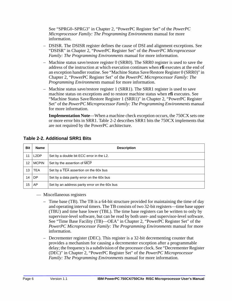
See “SPRG0–SPRG3" in Chapter 2, “PowerPC Register Set” of the PowerPC Microprocessor Family: The Programming Environments manual for more information.
– DSISR. The DSISR register defines the cause of DSI and alignment exceptions. See “DSISR" in Chapter 2, “PowerPC Register Set" of the PowerPC Microprocessor Family: The Programming Environments manual for more information.
– Machine status save/restore register 0 (SRR0). The SRR0 register is used to save the address of the instruction at which execution continues when rfi executes at the end of an exception handler routine. See “Machine Status Save/Restore Register 0 (SRR0)" in Chapter 2, “PowerPC Register Set" of the PowerPC Microprocessor Family: The Programming Environments manual for more information.
– Machine status save/restore register 1 (SRR1). The SRR1 register is used to save machine status on exceptions and to restore machine status when rfi executes. See “Machine Status Save/Restore Register 1 (SRR1)" in Chapter 2, “PowerPC Register Set" of the PowerPC Microprocessor Family: The Programming Environments manual for more information.
Implementation Note—When a machine check exception occurs, the 750CX sets one or more error bits in SRR1. Table 2-2 describes SRR1 bits the 750CX implements that are not required by the PowerPC architecture.
— Miscellaneous registers
– Time base (TB). The TB is a 64-bit structure provided for maintaining the time of day and operating interval timers. The TB consists of two 32-bit registers—time base upper (TBU) and time base lower (TBL). The time base registers can be written to only by supervisor-level software, but can be read by both user- and supervisor-level software. See “Time Base Facility (TB)—OEA" in Chapter 2, “PowerPC Register Set" of the PowerPC Microprocessor Family: The Programming Environments manual for more information.
– Decrementer register (DEC). This register is a 32-bit decrementing counter that provides a mechanism for causing a decrementer exception after a programmable delay; the frequency is a subdivision of the processor clock. See “Decrementer Register (DEC)" in Chapter 2, “PowerPC Register Set" of the PowerPC Microprocessor Family: The Programming Environments manual for more information.
Table 2-2. Additional SRR1 Bits
Bit Name Description
11 L2DP Set by a double bit ECC error in the L2.
12 MCPIN Set by the assertion of MCP
13 TEA Set by a TEA assertion on the 60x bus
14 DP Set by a data parity error on the 60x bus
15 AP Set by an address parity error on the 60x bus
Page 6 Version 1.1 IBM PowerPC 750CX/750CXe RISC Microprocessor User’s Manual

Implementation Note—In the 750CX, the decrementer register is decremented and the time base is incremented at a speed that is one-fourth the speed of the bus clock.
– Data address breakpoint register (DABR)—This optional register is used to cause a breakpoint exception if a specified data address is encountered. See “Data Address Breakpoint Register (DABR)" in Chapter 2, “PowerPC Register Set" of the PowerPC Microprocessor Family: The Programming Environments manual.”
– External access register (EAR). This optional register is used in conjunction with eciwx and ecowx. Note that the EAR register and the eciwx and ecowx instructions are optional in the PowerPC architecture and may not be supported in all PowerPC processors that implement the OEA. See “External Access Register (EAR)" in Chapter 2, “PowerPC Register Set" of the PowerPC Microprocessor Family: The Programming Environments manual for more information.
• 750CX-specific registers—The PowerPC architecture allows implementation-specific SPRs. Those incorporated in the 750CX are described as follows. Note that in the 750CX, these registers are all supervisor-level registers.
— Instruction address breakpoint register (IABR)—This register can be used to cause a breakpoint exception if a specified instruction address is encountered.
— Hardware implementation-dependent register 0 (HID0)—This register controls various functions, such as enabling checkstop conditions, and locking, enabling, and invalidating the instruction and data caches.
— Hardware implementation-dependent register 1 (HID1)—This register reflects the state of PLL_CFG[0–3] clock signals.
— The L2 cache control register (L2CR) is used to configure and operate the L2 cache.
— Performance monitor registers. The following registers are used to define and count events for use by the performance monitor:
– The performance monitor counter registers (PMC1–PMC4) are used to record the number of times a certain event has occurred. UPMC1–UPMC4 provide user-level read access to these registers.
– The monitor mode control registers (MMCR0–MMCR1) are used to enable various performance monitor interrupt functions. UMMCR0–UMMCR1 provide user-level read access to these registers.
– The sampled instruction address register (SIA) contains the effective address of an instruction executing at or around the time that the processor signals the performance monitor interrupt condition. USIA provides user-level read access to the SIA.
– The 750CX does not implement the sampled data address register (SDA) or the user-level, read-only USDA registers. However, for compatibility with processors that do, those registers can be written to by boot code without causing an exception. SDA is SPR 959; USDA is SPR 943.
— The instruction cache throttling control register (ICTC) has bits for enabling the instruction cache throttling feature and for controlling the interval at which instructions are forwarded to the instruction buffer in the fetch unit. This provides control over the processor’s overall junction temperature.
— Thermal management registers (THRM1, THRM2, and THRM3). Used to enable and set thresholds for the thermal management facility.
Table of Contents 5/9/02 Page 7

– THRM1 and THRM2 provide the ability to compare the junction temperature against two user-provided thresholds. The dual thresholds allow the thermal management software differing degrees of action in lowering the junction temperature. The TAU can be also operated in a single threshold mode in which the thermal sensor output is compared to only one threshold in either THRM1 or THRM2.
– THRM3 is used to enable the thermal management assist unit (TAU) and to control the comparator output sample time.
Note that while it is not guaranteed that the implementation of 750CX-specific registers is consistentamong PowerPC processors, other processors may implement similar or identical registers.
2.1.2 PowerPC 750CX-Specific RegistersThis section describes registers that are defined for the 750CX but are not included in the PowerPCarchitecture.
2.1.2.1 Instruction Address Breakpoint Register (IABR)The address breakpoint register (IABR), shown in Figure 2-2, supports the instruction addressbreakpoint exception. When this exception is enabled, instruction fetch addresses are compared withan effective address stored in the IABR. If the word specified in the IABR is fetched, the instructionbreakpoint handler is invoked. The instruction that triggers the breakpoint does not execute before thehandler is invoked. For more information, see Section 4.5.14 on Page 4-22. The IABR can beaccessed with mtspr and mfspr using the SPR1010.
Figure 2-2. Instruction Address Breakpoint Register
The IABR bits are described in Table 2-3.
2.1.2.2 Hardware Implementation-Dependent Register 0The hardware implementation-dependent register 0 (HID0) controls the state of several functionswithin the 750CX. The HID0 register is shown in Figure 2-3.
Table 2-3. Instruction Address Breakpoint Register Bit Settings
Bits Name Description
0–29 Address Word address to be compared
30 BE Breakpoint enabled. Setting this bit indicates that breakpoint checking is to be done.
31 TE Translation enabled. An IABR match is signaled if this bit matches MSR[IR].
0 29 30 31
Address BE TE
Page 8 Version 1.1 IBM PowerPC 750CX/750CXe RISC Microprocessor User’s Manual

Figure 2-3. Hardware Implementation-Dependent Register 0 (HID0)
The HID0 bits are described in Table 2-4.
Table 2-4. HID0 Bit Functions
Bit Name Function
0 EMCP Enable MCP. The primary purpose of this bit is to mask out further machine check exceptions caused by assertion of MCP, similar to how MSR[EE] can mask external interrupts.0 Masks MCP. Asserting MCP does not generate a machine check exception or a checkstop. 1 Asserting MCP causes checkstop if MSR[ME] = 0 or a machine check exception if ME = 1.
1 DBP Disable 60x bus address and data parity generation. 0 Parity generation is enabled.1 Disable parity generation. If the system does not use address or data parity and the respective
parity checking is disabled (HID0[EBA] or HID0[EBD] = 0), input receivers for those signals are disabled, require no pull-up resistors, and thus should be left unconnected. If all parity generation is disabled, all parity checking should also be disabled and parity signals need not be connected.
2 EBA Enable/disable 60x bus address parity checking 0 Prevents address parity checking.1 Allows a address parity error to cause a checkstop if MSR[ME] = 0 or a machine check exception if
MSR[ME] = 1.EBA and EBD allow the processor to operate with memory subsystems that do not generate parity.
3 EBD Enable 60x bus data parity checking0 Parity checking is disabled.1 Allows a data parity error to cause a checkstop if MSR[ME] = 0 or a machine check exception if
MSR[ME] = 1.EBA and EBD allow the processor to operate with memory subsystems that do not generate parity.
4 BCLK CKSTP_OUT enable. Used in conjunction with HID0[ECLK] and the HRESET signal to configure CKSTP_OUT. See Table 2-5 on Page 2-12.
5 — Not used. Defined as EICE on some earlier processors.
6 ECLK CKSTP_OUT enable. Used in conjunction with HID0[BCLK] and the HRESET signal to configure CKSTP_OUT. See Table 2-5 on Page 2-12.
7 PAR Disable precharge of ARTRY.0 Precharge of ARTRY enabled1 Alters bus protocol slightly by preventing the processor from driving ARTRY to high (negated)
state. If this is done, the system must restore the signals to the high state.
8 DOZE Doze mode enable. Operates in conjunction with MSR[POW].0 Doze mode disabled.1 Doze mode enabled. Doze mode is invoked by setting MSR[POW] while this bit is set. In doze
mode, the PLL, time base, and snooping remain active.
EBDEBA PAR NAP DPM NHR ICE DCE DCFI
EMCP BCLK ECLK DOZE SLEEP ILOCKDLOCK
ICFI SPD DCFA BTIC
0 1 2 3 4 5 6 7 8 9 10 11 12 13 14 15 16 17 18 19 20 21 22 23 24 25 26 27 28 29 30 31
Reserved
BHTABE00DBP 00 0IFEM SGE
NOOPTI
0
Table of Contents 5/9/02 Page 9

9 NAP Nap mode enable. Operates in conjunction with MSR[POW]. 0 Nap mode disabled.1 Nap mode enabled. Doze mode is invoked by setting MSR[POW] while this bit is set. In nap mode,
the PLL and the time base remain active.
10 SLEEP Sleep mode enable. Operates in conjunction with MSR[POW]. 0 Sleep mode disabled.1 Sleep mode enabled. Sleep mode is invoked by setting MSR[POW] while this bit is set. QREQ is
asserted to indicate that the processor is ready to enter sleep mode. If the system logic determines that the processor may enter sleep mode, the quiesce acknowledge signal, QACK, is asserted back to the processor. Once QACK assertion is detected, the processor enters sleep mode after several processor clocks. At this point, the system logic may turn off the PLL by first configuring PLL_CFG[0–3] to PLL bypass mode, then disabling SYSCLK.
11 DPM Dynamic power management enable.0 Dynamic power management is disabled.1 Functional units may enter a low-power mode automatically if the unit is idle. This does not affect
operational performance and is transparent to software or any external hardware.
12–14 — Not used
15 NHR Not hard reset (software-use only)—Helps software distinguish a hard reset from a soft reset. 0 A hard reset occurred if software had previously set this bit.1 A hard reset has not occurred. If software sets this bit after a hard reset, when a reset occurs and
this bit remains set, software can tell it was a soft reset.
16 ICE Instruction cache enable0 The instruction cache is neither accessed nor updated. All pages are accessed as if they were
marked cache-inhibited (WIM = X1X). Potential cache accesses from the bus (snoop and cache operations) are ignored. In the disabled state for the L1 caches, the cache tag state bits are ignored and all accesses are propagated to the L2 cache or bus as single-beat transactions. For those transactions, however, CI reflects the original state determined by address translation regardless of cache disabled status. ICE is zero at power-up.
1 The instruction cache is enabled
17 DCE Data cache enable0 The data cache is neither accessed nor updated. All pages are accessed as if they were marked
cache-inhibited (WIM = X1X). Potential cache accesses from the bus (snoop and cache operations) are ignored. In the disabled state for the L1 caches, the cache tag state bits are ignored and all accesses are propagated to the L2 cache or bus as single-beat transactions. For those transactions, however, CI reflects the original state determined by address translation regardless of cache disabled status. DCE is zero at power-up.
1 The data cache is enabled.
18 ILOCK Instruction cache lock0 Normal operation 1 Instruction cache is locked. A locked cache supplies data normally on a hit, but are treated as a
cache-inhibited transaction on a miss. On a miss, the transaction to the bus or the L2 cache is single-beat, however, CI still reflects the original state as determined by address translation independent of cache locked or disabled status.
To prevent locking during a cache access, an isync instruction must precede the setting of ILOCK.
Table 2-4. HID0 Bit Functions (Continued)
Bit Name Function
Page 10 Version 1.1 IBM PowerPC 750CX/750CXe RISC Microprocessor User’s Manual

19 DLOCK Data cache lock. 0 Normal operation1 Data cache is locked. A locked cache supplies data normally on a hit but is treated as a
cache-inhibited transaction on a miss. On a miss, the transaction to the bus or the L2 cache is single-beat, however, CI still reflects the original state as determined by address translation independent of cache locked or disabled status. A snoop hit to a locked L1 data cache performs as if the cache were not locked. A cache block invalidated by a snoop remains invalid until the cache is unlocked.
To prevent locking during a cache access, a sync instruction must precede the setting of DLOCK.
20 ICFI Instruction cache flash invalidate 0 The instruction cache is not invalidated. The bit is cleared when the invalidation operation begins
(usually the next cycle after the write operation to the register). The instruction cache must be enabled for the invalidation to occur.
1 An invalidate operation is issued that marks the state of each instruction cache block as invalid without writing back modified cache blocks to memory. Cache access is blocked during this time. Bus accesses to the cache are signaled as a miss during invalidate-all operations. Setting ICFI clears all the valid bits of the blocks and the PLRU bits to point to way L0 of each set. Once the L1 flash invalidate bits are set through a mtspr operations, hardware automatically resets these bits in the next cycle (provided that the corresponding cache enable bits are set in HID0).
Note, in the PowerPC 603 and PowerPC 603e processors, the proper use of the ICFI and DCFI bits was to set them and clear them in two consecutive mtspr operations. Software that already has this sequence of operations does not need to be changed to run on 750CX.
21 DCFI Data cache flash invalidate 0 The data cache is not invalidated. The bit is cleared when the invalidation operation begins (usually
the next cycle after the write operation to the register). The data cache must be enabled for the invalidation to occur.
1 An invalidate operation is issued that marks the state of each data cache block as invalid without writing back modified cache blocks to memory. Cache access is blocked during this time. Bus accesses to the cache are signaled as a miss during invalidate-all operations. Setting DCFI clears all the valid bits of the blocks and the PLRU bits to point to way L0 of each set. Once the L1 flash invalidate bits are set through a mtspr operations, hardware automatically resets these bits in the next cycle (provided that the corresponding cache enable bits are set in HID0).
Setting this bit clears all the valid bits of the blocks and the PLRU bits to point to way L0 of each set. Note, In the PowerPC 603 and PowerPC 603e processors, the proper use of the ICFI and DCFI bits was to set them and clear them in two consecutive mtspr operations. Software that already has this sequence of operations does not need to be changed to run on the 750CX.
22 SPD Speculative cache access disable0 Speculative bus accesses to nonguarded space (G = 0) from both the instruction and data caches
is enabled 1 Speculative bus accesses to nonguarded space in both caches is disabled
23 IFEM Enable M bit on bus for instruction fetches.0 M bit disabled. Instruction fetches are treated as nonglobal on the bus1 Instruction fetches reflect the M bit from the WIM settings.
24 SGE Store gathering enable0 Store gathering is disabled1 Integer store gathering is performed for write-through to nonguarded space or for cache-inhibited
stores to nonguarded space for 4-byte, word-aligned stores. The LSU combines stores to form a double word that is sent out on the 60x bus as a single-beat operation. Stores are gathered only if successive, eligible stores, are queued and pending. Store gathering is performed regardless of address order or endian mode.
Table 2-4. HID0 Bit Functions (Continued)
Bit Name Function
Table of Contents 5/9/02 Page 11

Table 2-5 shows how HID0[BCLK], HID0[ECLK], and HRESET are used to configureCKSTP_OUT. See Section 7.2.9.4 on Page 7-17 for more information.
25 DCFA Data cache flush assist. (Force data cache to ignore invalid sets on miss replacement selection.)0 The data cache flush assist facility is disabled.1 The miss replacement algorithm ignores invalid entries and follows the replacement sequence
defined by the PLRU bits. This reduces the series of uniquely addressed load or dcbz instructions to eight per set. The bit should be set just before beginning a cache flush routine and should be cleared when the series of instructions is complete.
26 BTIC Branch Target Instruction Cache enable— enables the 64-entry branch instruction cache.0 The BTIC is disabled, the contents are invalidated, and the BTIC behaves as if it was empty. New
entries cannot be added until the BTIC is enabled.1 The BTIC is enabled, and new entries can be added.
27 — Not used. Defined as FBIOB on earlier 603-type processors.
28 ABE Address broadcast enable—controls whether certain address-only operations (such as cache operations, eieio, and sync) are broadcast on the 60x bus. 0 Address-only operations affect only local L1 and L2 caches and are not broadcast. 1 Address-only operations are broadcast on the 60x bus.Affected instructions are eieio, sync, dcbi,
dcbf, and dcbst. A sync instruction completes only after a successful broadcast. Execution of eieio causes a broadcast that may be used to prevent any external devices, such as a bus bridge chip, from store gathering.
Note that dcbz (with M = 1, coherency required) always broadcasts on the 60x bus regardless of the setting of this bit. An icbi is never broadcast. No cache operations, except dcbz, are snooped by the 750CX regardless of whether the ABE is set. Bus activity caused by these instructions results directly from performing the operation on the 750CX cache.
29 BHT Branch history table enable.0 BHT disabled. The 750CX uses static branch prediction as defined by the PowerPC architecture
(UISA) for those branch instructions the BHT would have otherwise used to predict (that is, those that use the CR as the only mechanism to determine direction). For more information on static branch prediction, see “Conditional Branch Control,” in Chapter 4 of the PowerPC Microprocessor Family: The Programming Environments manual.
1 Allows the use of the 512-entry branch history table (BHT). The BHT is disabled at power-on reset. All entries are set to weakly, not-taken.
30 — Not used.
31 NOOPTI No-op the data cache touch instructions. 0 The dcbt and dcbtst instructions are enabled. 1 The dcbt and dcbtst instructions are no-oped globally.
Table 2-5. HID0[BCLK] and HID0[ECLK] CKSTP_OUT Configuration
HRESET HID0[ECLK] HID0[BCLK] CKSTP_OUT
Asserted x x Not Applicable
Negated 0 0 CKSTP_OUT
Negated 0 1 SYSCLK/ 2
Negated 1 0 Processor Core
Negated 1 1 SYSCLK
Table 2-4. HID0 Bit Functions (Continued)
Bit Name Function
Page 12 Version 1.1 IBM PowerPC 750CX/750CXe RISC Microprocessor User’s Manual

HID0 can be accessed with mtspr and mfspr using SPR1008.
2.1.2.3 Hardware Implementation-Dependent Register 1The hardware implementation-dependent register 1 (HID1) reflects the state of the PLL_CFG[0–3]signals. The HID1 bits are shown in Figure 2-4.
Figure 2-4. Hardware Implementation-Dependent Register 1 (HID1)
The HID1 bits are described in Table 2-6.
HID1 can be accessed with mtspr and mfspr using SPR 1009.
2.1.2.4 Performance Monitor RegistersThis section describes the registers used by the performance monitor, which is described inChapter 11, "Performance Monitor".
2.1.2.4.1 Monitor Mode Control Register 0 (MMCR0)The monitor mode control register 0 (MMCR0), shown in Figure 2-5, is a 32-bit SPR provided tospecify events to be counted and recorded. The MMCR0 can be accessed only in supervisor mode.User-level software can read the contents of MMCR0 by issuing an mfspr instruction to UMMCR0,described in the next section.
Figure 2-5. Monitor Mode Control Register 0 (MMCR0)
Table 2-6. HID1 Bit Functions
Bit(s) Name Description
0 PC0 PLL configuration bit 0 (read-only)
1 PC1 PLL configuration bit 1 (read-only)
2 PC2 PLL configuration bit 2 (read-only)
3 PC3 PLL configuration bit 3 (read-only)
4–31 — Reserved
Note: The clock configuration bits reflect the state of the PLL_CFG[0–3] signals.
PC2PC0
0 1 2 3 4 31
PC1
Reserved
PC3 00 00000000000000000000000000
INTONBITTRANS
DISCOUNT
PMC1INTCONTROLENINT
PMC2INTCONTROL
RTCSELECT
PMCTRIGGER
DMSDU PMC1SELECT PMC2SELECT
0 1 2 3 4 5 6 7 8 9 10 15 16 17 18 19 25 26 31
DPDIS DMR THRESHOLD
Table of Contents 5/9/02 Page 13

This register must be cleared at power up. Reading this register does not change its contents. The bitsof the MMCR0 register are described in Table 2-7.
Table 2-7. MMCR0 Bit Settings
Bit Name Description
0 DIS Disables counting unconditionally.0 The values of the PMCn counters can be changed by hardware. 1 The values of the PMCn counters cannot be changed by hardware.
1 DP Disables counting while in supervisor mode. 0 The PMCn counters can be changed by hardware.1 If the processor is in supervisor mode (MSR[PR] is cleared), the counters are not
changed by hardware.
2 DU Disables counting while in user mode. 0 The PMCn counters can be changed by hardware. 1 If the processor is in user mode (MSR[PR] is set), the PMCn counters are not
changed by hardware.
3 DMS Disables counting while MSR[PM] is set.0 The PMCn counters can be changed by hardware.1 If MSR[PM] is set, the PMCn counters are not changed by hardware.
4 DMR Disables counting while MSR(PM) is zero. 0 The PMCn counters can be changed by hardware.1 If MSR[PM] is cleared, the PMCn counters are not changed by hardware.
5 ENINT Enables performance monitor interrupt signaling.0 Interrupt signaling is disabled.1 Interrupt signaling is enabled.Cleared by hardware when a performance monitor interrupt is signaled. To re-enable these interrupt signals, software must set this bit after handling the performance monitor interrupt. The IPL ROM code clears this bit before passing control to the operating system.
6 DISCOUNT Disables counting of PMCn when a performance monitor interrupt is signaled (that is, ((PMCnINTCONTROL = 1) & (PMCn[0] = 1) & (ENINT = 1)) or the occurrence of an enabled time base transition with ((INTONBITTRANS =1) & (ENINT = 1)). 0 Signaling a performance monitor interrupt does not affect counting status of PMCn.1 The signaling of a performance monitor interrupt prevents changing of PMC1
counter. The PMCn counter do not change if PMC2COUNTCTL = 0.Because a time base signal could have occurred along with an enabled counter overflow condition, software should always reset INTONBITTRANS to zero, if the value in INTONBITTRANS was a one.
7–8 RTCSELECT 64-bit time base, bit selection enable.00 Pick bit 63 to count 01 Pick bit 55 to count 10 Pick bit 51 to count 11 Pick bit 47 to count
9 INTONBITTRANS Cause interrupt signaling on bit transition (identified in RTCSELECT) from off to on0 Do not allow interrupt signal if chosen bit transitions.1 Signal interrupt if chosen bit transitions.Software is responsible for setting and clearing INTONBITTRANS.
10–15 THRESHOLD Threshold value. 750CX supports all 6 bits, allowing threshold values from 0–63. The intent of the THRESHOLD support is to characterize L1 data cache misses.
Page 14 Version 1.1 IBM PowerPC 750CX/750CXe RISC Microprocessor User’s Manual

MMCR0 can be accessed with mtspr and mfspr using SPR 952.
2.1.2.4.2 User Monitor Mode Control Register 0 (UMMCR0)The contents of MMCR0 are reflected to UMMCR0, which can be read by user-level software.MMCR0 can be accessed with mfspr using SPR 936.
2.1.2.4.3 Monitor Mode Control Register 1 (MMCR1)The monitor mode control register 1 (MMCR1) functions as an event selector for performancemonitor counter registers 3 and 4 (PMC3 and PMC4). The MMCR1 register is shown in Figure 2-6.
Figure 2-6. Monitor Mode Control Register 1 (MMCR1)
Bits for MMCR1 are shown in Table 2-8; the corresponding events are described in Section 2.1.2.4.5below.
16 PMC1INTCONTROL Enables interrupt signaling due to PMC1 counter overflow.0 Disable PMC1 interrupt signaling due to PMC1 counter overflow1 Enable PMC1 Interrupt signaling due to PMC1 counter overflow
17 PMCINTCONTROL Enable interrupt signaling due to any PMC2–PMC4 counter overflow. Overrides the setting of DISCOUNT. 0 Disable PMC2–PMC4 interrupt signaling due to PMC2–PMC4 counter overflow.1 Enable PMC2–PMC4 interrupt signaling due to PMC2–PMC4 counter overflow.
18 PMCTRIGGER Can be used to trigger counting of PMC2–PMC4 after PMC1 has overflowed or after a performance monitor interrupt is signaled.0 Enable PMC2–PMC4 counting. 1 Disable PMC2–PMC4 counting until either PMC1[0] = 1 or a performance monitor
interrupt is signaled.
19–25 PMC1SELECT PMC1 input selector, 128 events selectable. See Table 2-9.
26–31 PMC2SELECT PMC2 input selector, 64 events selectable. See Table 2-9.
Table 2-8. MMCR1 Bits
Bits Name Description
0–4 PMC3SELECT PMC3 input selector. 32 events selectable. See Table 2-9 for defined selections.
5–9 PMC4SELECT PMC4 input selector. 32 events selectable. See Table 2-9 for defined selections.
10–31 — Reserved.
Table 2-7. MMCR0 Bit Settings (Continued)
Bit Name Description
0 4 5 10 31
PMC3SELECT
Reserved
PMC4SELECT 0 000000000000000000000
9
Table of Contents 5/9/02 Page 15

MMCR1 can be accessed with mtspr and mfspr using SPR 956. User-level software can read thecontents of MMCR1 by issuing an mfspr instruction to UMMCR1, described in the followingsection.
2.1.2.4.4 User Monitor Mode Control Register 1 (UMMCR1)The contents of MMCR1 are reflected to UMMCR1, which can be read by user-level software.MMCR1 can be accessed with mfspr using SPR 940.
2.1.2.4.5 Performance Monitor Counter Registers (PMC1–PMC4)PMC1–PMC4, shown in Figure 2-7, are 32-bit counters that can be programmed to generate interruptsignals when they overflow.
Figure 2-7. Performance Monitor Counter Registers (PMC1–PMC4)
The bits contained in the PMCn registers are described in Table 2-9.
Counters are considered to overflow when the high-order bit (the sign bit) becomes set; that is, theyreach the value 2147483648 (0x8000_0000). However, an interrupt is not signaled unless bothPMCn[INTCONTROL] and MMCR0[ENINT] are also set.
Note that the interrupts can be masked by clearing MSR[EE]; the interrupt signal condition may occurwith MSR[EE] cleared, but the exception is not taken until EE is set. Setting MMCR0[DISCOUNT]forces counters to stop counting when a counter interrupt occurs.
Software is expected to use mtspr to set PMC explicitly to nonoverflow values. If software sets anoverflow value, an erroneous exception may occur. For example, if both PMCn[INTCONTROL] andMMCR0[ENINT] are set and mtspr loads an overflow value, an interrupt signal may be generatedwithout any event counting having taken place.
The event to be monitored by PMC1 can be chosen by setting MMCR0[19–25]. The event to bemonitored by PMC2 can be chosen by setting MMCR0[26-31]. The event to be monitored by PMC3can be chosen by setting MMCR1[0-4]. The event to be monitored by PMC4 can be chosen by settingMMCR1[5-9]. The selected events are counted beginning when MMCR0 is set until either MMCR0is reset or a performance monitor interrupt is generated.
Table 11-5 on Page 11-6, Table 11-6 on Page 11-7, Table 11-7 on Page 11-8, and Table 11-8 on Page11-9 list the selectable events and their encodings.
Table 2-9. PMCn Bits
Bits Name Description
0 OV Overflow. When this bit is set it indicates that this counter has reached its maximum value.
1–31 Counter value Indicates the number of occurrences of the specified event.
OV
0 1 31
Counter Value
Page 16 Version 1.1 IBM PowerPC 750CX/750CXe RISC Microprocessor User’s Manual

The PMC registers can be accessed with mtspr and mfspr using following SPR numbers:
• PMC1 is SPR 953
• PMC2 is SPR 954
• PMC3 is SPR 957
• PMC4 is SPR 958
2.1.2.4.6 User Performance Monitor Counter Registers (UPMC1–UPMC4)The contents of the PMC1–PMC4 are reflected to UPMC1–UPMC4, which can be read by user-levelsoftware. The UPMC registers can be read with mfspr using the following SPR numbers:
• UPMC1 is SPR 937
• UPMC2 is SPR 938
• UPMC3 is SPR 941
• UPMC4 is SPR 942
2.1.2.4.7 Sampled Instruction Address Register (SIA) The sampled instruction address register (SIA) is a supervisor-level register that contains the effectiveaddress of an instruction executing at or around the time that the processor signals the performancemonitor interrupt condition. The SIA is shown in Figure 2-8.
Figure 2-8. Sampled Instruction Address Registers (SIA)
If the performance monitor interrupt is triggered by a threshold event, the SIA contains the exactinstruction (called the sampled instruction) that caused the counter to overflow.
If the performance monitor interrupt was caused by something besides a threshold event, the SIAcontains the address of the last instruction completed during that cycle. SIA can be accessed with themtspr and mfspr instructions using SPR 955.
2.1.2.4.8 User Sampled Instruction Address Register (USIA) The contents of SIA are reflected to USIA, which can be read by user-level software. USIA can beaccessed with the mfspr instructions using SPR 939.
2.1.2.4.9 Sampled Data Address Register (SDA) and User Sampled Data Address Register (USDA)
The 750CX does not implement the sampled data address register (SDA) or the user-level, read-onlyUSDA registers. However, for compatibility with processors that do, those registers can be written toby boot code without causing an exception. SDA is SPR 959; USDA is SPR 943.
0 31
Instruction Address
Table of Contents 5/9/02 Page 17

2.1.3 Instruction Cache Throttling Control Register (ICTC)Reducing the rate of instruction fetching can control junction temperature without the complexity andoverhead of dynamic clock control. System software can control instruction forwarding by writing anonzero value to the ICTC register, a supervisor-level register shown in Figure 2-9. The overalljunction temperature reduction comes from the dynamic power management of each functional unitwhen the 750CX is idle in between instruction fetches. PLL (phase-locked loop) and DLL(delay-locked loop) configurations are unchanged.
Figure 2-9. Instruction Cache Throttling Control Register (ICTC)
Table 2-10 describes the bit fields for the ICTC register.
Instruction cache throttling is enabled by setting ICTC[E] and writing the instruction forwardinginterval into ICTC[FI]. Enabling, disabling, and changing the instruction forwarding interval affectinstruction forwarding immediately.
The ICTC register can be accessed with the mtspr and mfspr instructions using SPR 1019.
2.1.4 Thermal Management Registers (THRM1–THRM3)The on-chip thermal management assist unit provides the following functions:
• Compares the junction temperature against user programmed thresholds
• Generates a thermal management interrupt if the temperature crosses the threshold
• Provides a way for a successive approximation routine to estimate junction temperature
Control and access to the thermal management assist unit is through the privileged mtspr/mfsprinstructions to the three THRM registers. THRM1 and THRM2, shown in Figure 2-10, provide theability to compare the junction temperature against two user-provided thresholds. Having dual
Table 2-10. ICTC Bit Settings
Bits Name Description
0–22 — Reserved
23–30 FI Instruction forwarding interval expressed in processor clocks.0x00 0 clock cycle.0x01 1 clock cycle..0xFF 255 clock cycles
31 E Cache throttling enable0 Disable instruction cache throttling.1 Enable instruction cache throttling.
0 22 23 30 31
EFI0 0000000000000000000000
Reserved
Page 18 Version 1.1 IBM PowerPC 750CX/750CXe RISC Microprocessor User’s Manual

thresholds allows thermal management software differing degrees of action in reducing junctiontemperature. Thermal management can use a single-threshold mode in which the thermal sensoroutput is compared to only one threshold in either THRM1 or THRM2.
Figure 2-10. Thermal Management Registers 1–2 (THRM1–THRM2)
The bits in THRM1 and THRM2 are described in Table 2-11.
If an mtspr affects a THRM register that contains operating parameters for an ongoing comparisonduring operation of the thermal assist unit, the respective TIV bits are cleared and the comparison isrestarted. Changing THRM3 forces the TIV bits of both THRM1 and THRM2 to 0, and restarts thecomparison if THRM3[E] is set.
Examples of valid THRM1/THRM2 bit settings are shown in Table 2-12.
Table 2-11. THRM1–THRM2 Bit Settings
Bits Field Description
0 TIN Thermal management interrupt bit. Read-only. This bit is set if the thermal sensor output crosses the threshold specified in the SPR. The state of TIN is valid only if TIV is set. The interpretation of TIN is controlled by TID. See Table 2-12.
1 TIV Thermal management interrupt valid. Read-only. This bit is set by the thermal assist logic to indicate that the thermal management interrupt (TIN) state is valid. See Table 2-12.
2–8 Threshold Threshold that the thermal sensor output is compared to. The range is 0°—127°C, and each bit represents 1°C. Note that this is not the resolution of the thermal sensor.
9–28 — Reserved. System software should clear these bits when writing to the THRMn SPRs.
29 TID Thermal management interrupt direction bit. Selects the result of the temperature comparison to set TIN and to assert a thermal management interrupt if TIE is set. If TID is cleared, TIN is set and an interrupt occurs if the junction temperature exceeds the threshold. If TID is set, TIN is set and an interrupt is indicated if the junction temperature is below the threshold. See Table 2-12 on Page 2-20.
30 TIE Thermal management interrupt enable. The thermal management interrupt is maskable by the MSR[EE] bit. If TIE is cleared and THRMn is valid, the TIN bit records the status of the junction temperature vs. threshold comparison without causing an exception. This lets system software successively approximate the junction temperature. See Table 2-12 on Page 2-20.
31 V SPR valid bit. Setting this bit indicates the SPR contains a valid threshold, TID and TIE controls bits. THRM1/2[V] = 1 and THRM3[E] = 1 enables the thermal sensor operation. See Table 2-12 on Page 2-20.
TIV THRESHOLD
0 1 2 8 9 28 29 30 31
TIDTIN
Reserved
TIE V0 0000000000000000000
Table of Contents 5/9/02 Page 19

The THRM3 register, shown in Figure 2-11, is used to enable the thermal assist unit and to controlthe comparator output sample time. The thermal assist logic manages the thermal managementinterrupt generation and time-multiplexed comparisons in dual-threshold mode as well as othercontrol functions.
Figure 2-11. Thermal Management Register 3 (THRM3)
The bits in THRM3 are described in Table 2-13.
Table 2-12. Valid THRM1/THRM2 Bit Settings
TIN1
1 TIN and TIV are read-only status bits.
TIV1 TID TIE V Description
x x x x 0 Invalid entry. The threshold in the SPR is not used for comparison.
x x x 0 1 Disable thermal management interrupt assertion.
x x 0 x 1 Set TIN and assert thermal management interrupt if TIE = 1 and the junction temperature exceeds the threshold.
x x 1 x 1 Set TIN and assert thermal management interrupt if TIE = 1 and the junction temperature is less than the threshold.
x 0 x x 1 The state of the TIN bit is not valid.
0 1 0 x 1 The junction temperature is less than the threshold and as a result the thermal management interrupt is not generated for TIE = 1.
1 1 0 x 1 The junction temperature is greater than the threshold and as a result the thermal management interrupt is generated if TIE = 1.
0 1 1 x 1 The junction temperature is greater than the threshold and as a result the thermal management interrupt is not generated for TIE = 1.
1 1 1 x 1 The junction temperature is less than the threshold and as a result the thermal management interrupt is generated if TIE = 1.
Note:
0 17 18 30 31
Reserved
ESampled Interval Timer Value0 00000000000000000
Page 20 Version 1.1 IBM PowerPC 750CX/750CXe RISC Microprocessor User’s Manual

The THRM registers can be accessed with the mtspr and mfspr instructions using the following SPRnumbers:
• THRM1 is SPR 1020
• THRM2 is SPR 1021
• THRM3 is SPR 1022
2.1.5 L2 Cache Control Register (L2CR)The L2 cache control register, shown in Figure 2-12, is a supervisor-level, implementation-specificSPR used to configure and operate the L2 cache. It is cleared by a hard reset or power-on reset.
Figure 2-12. L2 Cache Control Register (L2CR)
The L2 cache interface is described in Chapter 9, "L2 Cache",
The L2CR bits are described in the following table.
Table 2-13. THRM3 Bit Settings
Bits Name Description
0–17 — Reserved for future use. System software should clear these bits when writing to the THRM3.
18–30 SITV Sample interval timer value. Number of elapsed processor clock cycles before a junction temperature vs. threshold comparison result is sampled for TIN bit setting and interrupt generation. This is necessary due to the thermal sensor, DAC, and the analog comparator settling time being greater than the processor cycle time. The value should be configured to allow a sampling interval of 20 microseconds.
31 E Enables the thermal sensor compare operation if either THRM1[V] or THRM2[V] is set.
0 1 2 8 9 10 11 12 13 14 30 31
L2E
L2CE
L2WT
L2I
L2DO L2TS L2IPReserved
00000 0 00 0 0 0 0 0 0 0 0 000000000
Table of Contents 5/9/02 Page 21

The L2CR register can be accessed with the mtspr and mfspr instructions using SPR 1017.
2.2 Operand ConventionsThis section describes the operand conventions as they are represented in two levels of the PowerPCarchitecture—UISA and VEA. Detailed descriptions of conventions used for storing values inregisters and memory, accessing PowerPC registers, and representation of data in these registers canbe found in Chapter 3, “Operand Conventions" in the PowerPC Microprocessor Family: TheProgramming Environments manual.
Table 2-14. L2CR Bit Settings
Bit Name Function
0 L2E L2 enable. Enables L2 cache operation (including snooping) starting with the next transaction the L2 cache unit receives. Before enabling the L2 cache, all other L2CR bits must be set appropriately. The L2 cache may need to be invalidated globally.
1 L2CE L2 Checkstop enable.0 ECC double bit error does not cause a Machine Check.1 ECC double bit error causes a machine check exception.
2–8 — Reserved.
9 L2DO L2 data-only. Setting this bit enables data-only operation in the L2 cache. For this operation, only transactions from the L1 data cache can be cached in the L2 cache, which treats all transactions from the L1 instruction cache as cache-inhibited (bypass L2 cache, no L2 checking done). This bit is provided for L2 testing only.
10 L2I L2 global invalidate. Setting L2I invalidates the L2 cache globally by clearing the L2 bits including status bits. This bit must not be set while the L2 cache is enabled.
11 — Reserved.
12 L2WT L2 write-through. Setting L2WT selects write-through mode (rather than the default write-back mode) so all writes to the L2 cache also write through to the 60x bus. For these writes, the L2 cache entry is always marked as clean (valid unmodified) rather than dirty (valid modified). This bit must never be asserted after the L2 cache has been enabled as previously-modified lines can get remarked as clean during normal operation.
13 L2TS L2 test support. Setting L2TS causes cache block pushes from the L1 data cache that result from dcbf and dcbst instructions to be written only into the L2 cache and marked valid, rather than being written only to the 60x bus and marked invalid in the L2 cache in case of hit. This bit allows a dcbz/dcbf instruction sequence to be used with the L1 cache enabled to easily initialize the L2 cache with any address and data information. This bit also keeps dcbz instructions from being broadcast on the 60x and single-beat cacheable store misses in the L2 from being written to the 60x bus.
14–30 — Reserved.
31 L2IP L2 global invalidate in progress (read only). This read-only bit indicates whether an L2 global invalidate is occurring. It should be monitored after an L2 global invalidate has been initiated by the L2I bit to determine when it has completed.
Page 22 Version 1.1 IBM PowerPC 750CX/750CXe RISC Microprocessor User’s Manual

2.2.1 Data Organization in Memory and Data TransfersBytes in memory are numbered consecutively starting with 0. Each number is the address of thecorresponding byte.
Memory operands may be bytes, half words, words, or double words, or, for the load/store multipleand load/store string instructions, a sequence of bytes or words. The address of a memory operand isthe address of its first byte (that is, of its lowest-numbered byte). Operand length is implicit for eachinstruction.
2.2.2 Alignment and Misaligned AccessesThe operand of a single-register memory access instruction has an alignment boundary equal to itslength. An operand’s address is misaligned if it is not a multiple of its width. Operands forsingle-register memory access instructions have the characteristics shown in Table 2-15. Althoughnot permitted as memory operands, quad words are shown because quad-word alignment is desirablefor certain memory operands.
The concept of alignment is also applied more generally to data in memory. For example, a 12-bytedata item is said to be word-aligned if its address is a multiple of four.
Some instructions require their memory operands to have certain alignment. In addition, alignmentmay affect performance. For single-register memory access instructions, the best performance isobtained when memory operands are aligned.
Instructions are 32 bits (one word) long and must be word-aligned.
The 750CX does not provide hardware support for floating-point memory that is not word-aligned.If a floating-point operand is not aligned, the 750CX invokes an alignment exception, and it is left upto software to break up the offending storage access operation appropriately. In addition, somenon-double-word–aligned memory accesses suffer performance degradation as compared to analigned access of the same type.
In general, floating-point word accesses should always be word-aligned and floating-pointdouble-word accesses should always be double-word–aligned. Frequent use of misaligned accessesis discouraged since they can degrade overall performance.
Table 2-15. Memory Operands
Operand LengthAddr[28-31]If Aligned
Byte 8 bits xxxx
Half word 2 bytes xxx0
Word 4 bytes xx00
Double word 8 bytes x000
Quad word 16 bytes 0000
Note: An “x” in an address bit position indicates that the bit can be 0 or 1 independent of the state of other bits in the address.
Table of Contents 5/9/02 Page 23

2.2.3 Floating-Point Operand and Execution Models—UISAThe IEEE 754 standard defines conventions for 64- and 32-bit arithmetic. The standard requires thatsingle-precision arithmetic be provided for single-precision operands. The standard permitsdouble-precision arithmetic instructions to have either (or both) single-precision or double-precisionoperands, but states that single-precision arithmetic instructions should not accept double-precisionoperands.
The PowerPC UISA follows these guidelines:
• Double-precision arithmetic instructions may have single-precision operands but always produce double-precision results.
• Single-precision arithmetic instructions require all operands to be single-precision and always produce single-precision results.
For arithmetic instructions, conversion from double- to single-precision must be done explicitly bysoftware, while conversion from single- to double-precision is done implicitly by the processor.
All PowerPC implementations provide the equivalent of the execution models described in Section3.3 of the PowerPC Microprocessor Family: The Programming Environments manual to ensure thatidentical results are obtained. The definition of the arithmetic instructions for infinities, denormalizednumbers, and NaNs follow conventions described in that section.
Although the double-precision format specifies an 11-bit exponent, exponent arithmetic uses twoadditional bit positions to avoid potential transient overflow conditions. An extra bit is required whendenormalized double-precision numbers are prenormalized. A second bit is required to permitcomputation of the adjusted exponent value in the following examples when the correspondingexception enable bit is one:
• Underflow during multiplication using a denormalized operand
• Overflow during division using a denormalized divisor
The 750CX provides hardware support for all single- and double-precision floating-point operationsfor most value representations and all rounding modes. This architecture provides for hardware toimplement a floating-point system as defined in ANSI/IEEE standard 754-1985, IEEE Standard forBinary Floating Point Arithmetic. Detailed information about the floating-point execution model canbe found in Chapter 3, “Operand Conventions" in the PowerPC Microprocessor Family: TheProgramming Environments manual.
The 750CX supports non-IEEE mode whenever FPSCR[29] is set. In this mode, denormalizednumbers, NaNs, and some IEEE invalid operations are treated in a non-IEEE conforming manner.This is accomplished by delivering results that approximate the values required by the IEEE standard.
Page 24 Version 1.1 IBM PowerPC 750CX/750CXe RISC Microprocessor User’s Manual

.
Table 2-16. Floating-Point Operand Data Type Behavior
Operand A Data Type
Operand B Data Type
Operand C Data Type
IEEE Mode(NI = 0)
Non-IEEE Mode(NI = 1)
Single denormalizedDouble denormalized
Single denormalizedDouble denormalized
Single denormalizedDouble denormalized
Normalize all three Zero all three
Single denormalizedDouble denormalized
Single denormalizedDouble denormalized
Normalized or zero Normalize A and B Zero A and B
Normalized or zero Single denormalizedDouble denormalized
Single denormalizedDouble denormalized
Normalize B and C Zero B and C
Single denormalizedDouble denormalized
Normalized or zero Single denormalizedDouble denormalized
Normalize A and C Zero A and C
Single denormalizedDouble denormalized
Normalized or zero Normalized or zero Normalize A Zero A
Normalized or zero Single denormalizedDouble denormalized
Normalized or zero Normalize B Zero B
Normalized or zero Normalized or zero Single denormalizedDouble denormalized
Normalize C Zero C
Single QNaNSingle SNaNDouble QNaNDouble SNaN
Don’t care Don’t care QNaN1 QNaN1
Don’t care Single QNaNSingle SNaNDouble QNaNDouble SNaN
Don’t care QNaN1 QNaN1
Don’t care Don’t care Single QNaNSingle SNaNDouble QNaNDouble SNaN
QNaN1 QNaN1
Single normalizedSingle infinitySingle zeroDouble normalizedDouble infinityDouble zero
Single normalizedSingle infinitySingle zeroDouble normalizedDouble infinityDouble zero
Single normalizedSingle infinitySingle zeroDouble normalizedDouble infinityDouble zero
Do the operation Do the operation
1 Prioritize according to Chapter 3, “Operand Conventions,” in the PowerPC Microprocessor Family: The Programming Environments manual.
Table of Contents 5/9/02 Page 25

Table 2-17 summarizes the mode behavior for results.
2.3 Instruction Set SummaryThis chapter describes instructions and addressing modes defined for the 750CX. These instructionsare divided into the following functional categories:
• Integer instructions—These include arithmetic and logical instructions. For more information, see Section 2.3.4.1 on Page 2-32.
• Floating-point instructions—These include floating-point arithmetic instructions (single-precision and double-precision), as well as instructions that affect the floating-point status and control register (FPSCR). For more information, see Section 2.3.4.2 on Page 2-36.
• Load and store instructions—These include integer and floating-point (including quantized) load and store instructions. For more information, see Section 2.3.4.3 on Page 2-40.
• Flow control instructions—These include branching instructions, condition register logical instructions, trap instructions, and other instructions that affect the instruction flow. For more information, see Section 2.3.4.4 on Page 2-49.
• Processor control instructions—These instructions are used for synchronizing memory accesses and managing caches, TLBs, and segment registers. For more information, see Section 2.3.4.6 on Page 2-51, Section 2.3.5.1 on Page 2-56, and Section 2.3.6.2 on Page 2-61.
• Memory synchronization instructions—These instructions are used for memory synchronizing. For more information, see Section 2.3.4.7 on Page 2-54 and Section 2.3.5.2 on Page 2-56.
• Memory control instructions—These instructions provide control of caches, TLBs, and segment registers. For more information, see Section 2.3.5.3 on Page 2-57 and Section 2.3.6.3 on Page 2-61.
Table 2-17. Floating-Point Result Data Type Behavior
Precision Data Type IEEE Mode (NI = 0) Non-IEEE Mode (NI = 1)
Single Denormalized Return single-precision denormalized number with trailing zeros.
Return zero.
Single Normalized, infinity, zero
Return the result. Return the result.
Single QNaN, SNaN Return QNaN. Return QNaN.
Single INT Place integer into low word of FPR. If (Invalid Operation)then
Place (0x8000) into FPR[32–63]else
Place integer into FPR[32–63].
Double Denormalized Return double-precision denormalized number. Return zero.
Double Normalized, infinity, zero
Return the result. Return the result.
Double QNaN, SNaN Return QNaN. Return QNaN.
Double INT Not supported by 750CX Not supported by 750CX
Page 26 Version 1.1 IBM PowerPC 750CX/750CXe RISC Microprocessor User’s Manual

• External control instructions—These include instructions for use with special input/output devices. For more information, see Section 2.3.5.4 on Page 2-59.
NOTE: This grouping of instructions does not necessarily indicate the execution unit that processes a particular instruction or group of instructions. That information, which is useful for scheduling instructions most effectively, is provided in Chapter 6, "Instruction Timing".
Integer instructions operate on word operands. Floating-point instructions operate on single-precisionand double-precision floating-point operands. The PowerPC architecture uses instructions that arefour bytes long and word-aligned. It provides for byte, half-word, and word operand loads and storesbetween memory and a set of 32 general-purpose registers (GPRs). It provides for word anddouble-word operand loads and stores between memory and a set of 32 floating-point registers(FPRs).
Arithmetic and logical instructions do not read or modify memory. To use the contents of a memorylocation in a computation and then modify the same or another memory location, the memorycontents must be loaded into a register, modified, and then written to the target location using loadand store instructions.
The description of each instruction includes the mnemonic and a formatted list of operands. Tosimplify assembly language programming, a set of simplified mnemonics and symbols is providedfor some of the frequently-used instructions; see Appendix F, “Simplified Mnemonics,” in thePowerPC Microprocessor Family: The Programming Environments manual for a complete list ofsimplified mnemonics. Note that the architecture specification refers to simplified mnemonics asextended mnemonics. Programs written to be portable across the various assemblers for the PowerPCarchitecture should not assume the existence of mnemonics not described in that document.
2.3.1 Classes of InstructionsThe 750CX instructions belong to one of the following three classes.
• Defined
• Illegal
• Reserved
Note that while the definitions of these terms are consistent among the PowerPC processors, theassignment of these classifications is not. For example, PowerPC instructions defined for 64-bitimplementations are treated as illegal by 32-bit implementations such as the 750CX.
The class is determined by examining the primary opcode and the extended opcode, if any. If theopcode, or combination of opcode and extended opcode, is not that of a defined instruction or of areserved instruction, the instruction is illegal.
Instruction encodings that are now illegal may become assigned to instructions in the architecture ormay be reserved by being assigned to processor-specific instructions.
2.3.1.1 Definition of Boundedly UndefinedIf instructions are encoded with incorrectly set bits in reserved fields, the results on execution can besaid to be boundedly undefined. If a user-level program executes the incorrectly coded instruction,
Table of Contents 5/9/02 Page 27

the resulting undefined results are bounded in that a spurious change from user to supervisor state isnot allowed, and the level of privilege exercised by the program in relation to memory access andother system resources cannot be exceeded. Boundedly-undefined results for a given instruction mayvary between implementations, and between execution attempts in the same implementation.
2.3.1.2 Defined Instruction ClassDefined instructions are guaranteed to be supported in all PowerPC implementations, except as statedin the instruction descriptions in Chapter 12, "Instruction Set". The 750CX provides hardwaresupport for all instructions defined for 32-bit implementations.
It does not support the optional fsqrt, fsqrts, and tlbia instructions.
A PowerPC processor invokes the illegal instruction error handler (part of the program exception)when the unimplemented PowerPC instructions are encountered so they may be emulated in software,as required. Note that the architecture specification refers to exceptions as interrupts.
A defined instruction can have invalid forms. The 750CX provides limited support for instructionsrepresented in an invalid form.
2.3.1.3 Illegal Instruction ClassIllegal instructions can be grouped into the following categories:
• Instructions not defined in the PowerPC architecture.The following primary opcodes are defined as illegal but may be used in future extensions to the architecture:1, 4, 5, 6, 9, 22, 56, 60, 61
Future versions of the PowerPC architecture may define any of these instructions to perform new functions.
• Instructions defined in the PowerPC architecture but not implemented in a specific PowerPC implementation. For example, instructions that can be executed on 64-bit PowerPC processors are considered illegal by 32-bit processors such as the 750CX.
The following primary opcodes are defined for 64-bit implementations only and are illegal on the 750CX: 2, 30, 58, 62
• All unused extended opcodes are illegal. The unused extended opcodes can be determined from information in Section A.1 and Section 2.3.1.4 on Page 2-29. Notice that extended opcodes for instructions defined only for 64-bit implementations are illegal in 32-bit implementations, and vice versa. The following primary opcodes have unused extended opcodes.
17, 19, 31, 59, 63 (Primary opcodes 30 and 62 are illegal for all 32-bit implementations, but as 64-bit opcodes they have some unused extended opcodes.)
• An instruction consisting of only zeros is guaranteed to be an illegal instruction. This increases the probability that an attempt to execute data or uninitialized memory invokes the system illegal instruction error handler (a program exception). Note that if only the primary opcode consists of all zeros, the instruction is considered a reserved instruction, as described in Section 2.3.1.4.
The 750CX invokes the system illegal instruction error handler (a program exception) when it detectsany instruction from this class or any instructions defined only for 64-bit implementations.
Page 28 Version 1.1 IBM PowerPC 750CX/750CXe RISC Microprocessor User’s Manual

See Section 4.5.7 on Page 4-19 for additional information about illegal and invalid instructionexceptions. Except for an instruction consisting of binary zeros, illegal instructions are available foradditions to the PowerPC architecture.
2.3.1.4 Reserved Instruction ClassReserved instructions are allocated to specific implementation-dependent purposes not defined by thePowerPC architecture. Attempting to execute an unimplemented reserved instruction invokes theillegal instruction error handler (a program exception). See Section 4.5.7 on Page 4-19 forinformation about illegal and invalid instruction exceptions.
The PowerPC architecture defines four types of reserved instructions:
• Instructions in the POWER architecture not part of the PowerPC UISA. For details on POWER architecture incompatibilities and how they are handled by PowerPC processors, see Appendix B, “POWER Architecture Cross Reference" in the PowerPC Microprocessor Family: The Programming Environments manual.
• Implementation-specific instructions required for the processor to conform to the PowerPC architecture (none of these are implemented in the 750CX)
• All other implementation-specific instructions
• Architecturally-allowed extended opcodes
2.3.2 Addressing ModesThis section provides an overview of conventions for addressing memory and for calculating effectiveaddresses as defined by the PowerPC architecture for 32-bit implementations. For more detailedinformation, see “Conventions” in Chapter 4, “Addressing Modes and Instruction Set Summary" ofthe PowerPC Microprocessor Family: The Programming Environments manual.
2.3.2.1 Memory Addressing A program references memory using the effective (logical) address computed by the processor whenit executes a memory access or branch instruction or when it fetches the next sequential instruction.
Bytes in memory are numbered consecutively starting with zero. Each number is the address of thecorresponding byte.
2.3.2.2 Memory OperandsMemory operands may be bytes, half words, words, or double words, or, for the load/store multipleand load/store string instructions, a sequence of bytes or words. The address of a memory operand isthe address of its first byte (that is, of its lowest-numbered byte). Operand length is implicit for eachinstruction. The PowerPC architecture supports both big-endian and little-endian byte ordering. Thedefault byte and bit ordering is big-endian. See “Byte Ordering" in Chapter 3, “Operand Conventions”of the PowerPC Microprocessor Family: The Programming Environments manual for moreinformation about big- and little-endian byte ordering.
The operand of a single-register memory access instruction has a natural alignment boundary equalto the operand length. In other words, the “natural” address of an operand is an integral multiple ofthe operand length. A memory operand is said to be aligned if it is aligned at its natural boundary;otherwise it is misaligned.
Table of Contents 5/9/02 Page 29

For a detailed discussion about memory operands, see Chapter 3, “Operand Conventions” of thePowerPC Microprocessor Family: The Programming Environments manual.
2.3.2.3 Effective Address CalculationAn effective address is the 32-bit sum computed by the processor when executing a memory accessor branch instruction or when fetching the next sequential instruction. For a memory accessinstruction, if the sum of the effective address and the operand length exceeds the maximum effectiveaddress, the memory operand is considered to wrap around from the maximum effective addressthrough effective address 0, as described in the following paragraphs.
Effective address computations for both data and instruction accesses use 32-bit signed 2’scomplement binary arithmetic. A carry from bit 0 and overflow are ignored.
Load and store operations have the following modes of effective address generation:
• EA = (rA|0) + offset (including offset = 0) (register indirect with immediate index)
• EA = (rA|0) + rB (register indirect with index)
Refer to Section 2.3.4.3.2 on Page 2-41 for a detailed description of effective address generation forload and store operations.
Branch instructions have three categories of effective address generation:
• Immediate
• Link register indirect
• Count register indirect
2.3.2.4 Synchronization The synchronization described in this section refers to the state of the processor that is performing thesynchronization.
2.3.2.4.1 Context SynchronizationThe System Call (sc) and Return from Interrupt (rfi) instructions perform context synchronization byallowing previously issued instructions to complete before performing a change in context. Executionof one of these instructions ensures the following:
• No higher priority exception exists (sc).
• All previous instructions have completed to a point where they can no longer cause an exception. If a prior memory access instruction causes direct-store error exceptions, the results are guaranteed to be determined before this instruction is executed.
• Previous instructions complete execution in the context (privilege, protection, and address translation) under which they were issued.
• The instructions following the sc or rfi instruction execute in the context established by these instructions.
2.3.2.4.2 Execution SynchronizationAn instruction is execution synchronizing if all previously initiated instructions appear to havecompleted before the instruction is initiated or, in the case of sync and isync, before the instruction
Page 30 Version 1.1 IBM PowerPC 750CX/750CXe RISC Microprocessor User’s Manual

completes. For example, the Move to Machine State Register (mtmsr) instruction is executionsynchronizing. It ensures that all preceding instructions have completed execution and cannot causean exception before the instruction executes, but does not ensure subsequent instructions execute inthe newly established environment. For example, if the mtmsr sets the MSR[PR] bit, unless an isyncimmediately follows the mtmsr instruction, a privileged instruction could be executed or privilegedaccess could be performed without causing an exception even though the MSR[PR] bit indicates usermode.
2.3.2.4.3 Instruction-Related Exceptions There are two kinds of exceptions in 750CX—those caused directly by the execution of an instructionand those caused by an asynchronous event (or interrupts). Either may cause components of thesystem software to be invoked.
Exceptions can be caused directly by the execution of an instruction as follows:
• An attempt to execute an illegal instruction causes the illegal instruction (program exception) handler to be invoked. An attempt by a user-level program to execute the supervisor-level instructions listed below causes the privileged instruction (program exception) handler to be invoked. The 750CX provides the following supervisor-level instructions: dcbi, mfmsr, mfspr, mfsr, mfsrin, mtmsr, mtspr, mtsr, mtsrin, rfi, tlbie, and tlbsync. Note that the privilege level of the mfspr and mtspr instructions depends on the SPR encoding.
• Any mtspr, mfspr, or mftb instruction with an invalid SPR (or TBR) field causes an illegal type program exception. Likewise, a program exception is taken if user-level software tries to access a supervisor-level SPR. An mtspr instruction executing in supervisor mode (MSR[PR] = 0) with the SPR field specifying HID1 or PVR (read-only registers) executes as a no-op.
• An attempt to access memory that is not available (page fault) causes the ISI or DSI exception handler to be invoked.
• The execution of an sc instruction invokes the system call exception handler that permits a program to request the system to perform a service.
• The execution of a trap instruction invokes the program exception trap handler.
• The execution of an instruction that causes a floating-point exception while exceptions are enabled in the MSR invokes the program exception handler.
A detailed description of exception conditions is provided in Chapter 4, "Exceptions".
2.3.3 Instruction Set OverviewThis section provides a brief overview of the PowerPC instructions implemented in 750CX andhighlights any special information with respect to how 750CX implements a particular instruction.Note that the categories used in this section correspond to those used in Chapter 4, “AddressingModes and Instruction Set Summary” in the PowerPC Microprocessor Family: The ProgrammingEnvironments manual. These categorizations are somewhat arbitrary and are provided for theconvenience of the programmer and do not necessarily reflect the PowerPC architecture specification.
Note that some instructions have the following optional features:
• CR Update—The dot (.) suffix on the mnemonic enables the update of the CR.
• Overflow option—The o suffix indicates that the overflow bit in the XER is enabled.
Table of Contents 5/9/02 Page 31

2.3.4 PowerPC UISA InstructionsThe PowerPC UISA includes the base user-level instruction set (excluding a few user-level cachecontrol, synchronization, and time base instructions), user-level registers, programming model, datatypes, and addressing modes. This section discusses the instructions defined in the UISA.
2.3.4.1 Integer InstructionsThis section describes the integer instructions. These consist of the following:
• Integer arithmetic instructions
• Integer compare instructions
• Integer logical instructions
• Integer rotate and shift instructions
Integer instructions use the content of the GPRs as source operands and place results into GPRs, intothe integer exception register (XER), and into condition register (CR) fields.
2.3.4.1.1 Integer Arithmetic InstructionsTable 2-18 lists the integer arithmetic instructions for the PowerPC processors.
Page 32 Version 1.1 IBM PowerPC 750CX/750CXe RISC Microprocessor User’s Manual

Although there is no Subtract Immediate instruction, its effect can be achieved by using an addiinstruction with the immediate operand negated. Simplified mnemonics are provided that include thisnegation. The subf instructions subtract the second operand (rA) from the third operand (rB).Simplified mnemonics are provided in which the third operand is subtracted from the second operand.See Appendix F, “Simplified Mnemonics,” in the PowerPC Microprocessor Family: TheProgramming Environments manual for examples.
The UISA states that an implementation that executes instructions that set the overflow enable bit(OE) or the carry bit (CA) may either execute these instructions slowly or prevent execution of thesubsequent instruction until the operation completes. Chapter 6 describes how the 750CX handles CRdependencies. The summary overflow bit (SO) and overflow bit (OV) in the integer exception registerare set to reflect an overflow condition of a 32-bit result. This can happen only when OE = 1.
Table 2-18. Integer Arithmetic Instructions
Name Mnemonic Syntax
Add Immediate addi rD,rA,SIMM
Add Immediate Shifted addis rD,rA,SIMM
Add add (add. addo addo.) rD,rA,rB
Subtract From subf (subf. subfo subfo.) rD,rA,rB
Add Immediate Carrying addic rD,rA,SIMM
Add Immediate Carrying and Record addic. rD,rA,SIMM
Subtract from Immediate Carrying subfic rD,rA,SIMM
Add Carrying addc (addc. addco addco.) rD,rA,rB
Subtract from Carrying subfc (subfc. subfco subfco.) rD,rA,rB
Add Extended adde (adde. addeo addeo.) rD,rA,rB
Subtract from Extended subfe (subfe. subfeo subfeo.) rD,rA,rB
Add to Minus One Extended addme (addme. addmeo addmeo.) rD,rA
Subtract from Minus One Extended subfme (subfme. subfmeo subfmeo.) rD,rA
Add to Zero Extended addze (addze. addzeo addzeo.) rD,rA
Subtract from Zero Extended subfze (subfze. subfzeo subfzeo.) rD,rA
Negate neg (neg. nego nego.) rD,rA
Multiply Low Immediate mulli rD,rA,SIMM
Multiply Low mullw (mullw. mullwo mullwo.) rD,rA,rB
Multiply High Word mulhw (mulhw.) rD,rA,rB
Multiply High Word Unsigned mulhwu (mulhwu.) rD,rA,rB
Divide Word divw (divw. divwo divwo.) rD,rA,rB
Divide Word Unsigned divwu divwu. divwuo divwuo. rD,rA,rB
Table of Contents 5/9/02 Page 33

2.3.4.1.2 Integer Compare InstructionsThe integer compare instructions algebraically or logically compare the contents of register rA witheither the zero-extended value of the UIMM operand, the sign-extended value of the SIMM operand,or the contents of register rB. The comparison is signed for the cmpi and cmp instructions, andunsigned for the cmpli and cmpl instructions.
Table 2-19 summarizes the integer compare instructions.
The crfD operand can be omitted if the result of the comparison is to be placed in CR0. Otherwisethe target CR field must be specified in crfD, using an explicit field number.
For information on simplified mnemonics for the integer compare instructions see Appendix F,“Simplified Mnemonics,” in the PowerPC Microprocessor Family: The Programming Environmentsmanual.
2.3.4.1.3 Integer Logical InstructionsThe logical instructions shown in Table 2-20 perform bit-parallel operations on the specifiedoperands. Logical instructions with the CR updating enabled (uses dot suffix) and instructions andi.and andis. set CR field CR0 to characterize the result of the logical operation. Logical instructions donot affect XER[SO], XER[OV], or XER[CA].
See Appendix F, “Simplified Mnemonics,” in the PowerPC Microprocessor Family: TheProgramming Environments manual for simplified mnemonic examples for integer logicaloperations.
Table 2-19. Integer Compare Instructions
Name Mnemonic Syntax
Compare Immediate cmpi crfD,L,rA,SIMM
Compare cmp crfD,L,rA,rB
Compare Logical Immediate cmpli crfD,L,rA,UIMM
Compare Logical cmpl crfD,L,rA,rB
Table 2-20. Integer Logical Instructions
Name Mnemonic Syntax Implementation Notes
AND Immediate andi. rA,rS,UIMM —
AND Immediate Shifted andis. rA,rS,UIMM —
OR Immediate ori rA,rS,UIMM The PowerPC architecture defines ori r0,r0,0 as the preferred form for the no-op instruction. The dispatcher discards this instruction (except for pending trace or breakpoint exceptions).
OR Immediate Shifted oris rA,rS,UIMM —
XOR Immediate xori rA,rS,UIMM —
XOR Immediate Shifted xoris rA,rS,UIMM —
Page 34 Version 1.1 IBM PowerPC 750CX/750CXe RISC Microprocessor User’s Manual

2.3.4.1.4 Integer Rotate InstructionsRotation operations are performed on data from a GPR, and the result, or a portion of the result, isreturned to a GPR. See Appendix F, “Simplified Mnemonics,” in the PowerPC MicroprocessorFamily: The Programming Environments manual for a complete list of simplified mnemonics thatallows simpler coding of often-used functions such as clearing the leftmost or rightmost bits of aregister, left justifying or right justifying an arbitrary field, and simple rotates and shifts.
Integer rotate instructions rotate the contents of a register. The result of the rotation is either insertedinto the target register under control of a mask (if a mask bit is 1 the associated bit of the rotated datais placed into the target register, and if the mask bit is 0 the associated bit in the target register isunchanged), or ANDed with a mask before being placed into the target register.
The integer rotate instructions are summarized in Table 2-21.
AND and (and.) rA,rS,rB —
OR or (or.) rA,rS,rB —
XOR xor (xor.) rA,rS,rB —
NAND nand (nand.) rA,rS,rB —
NOR nor (nor.) rA,rS,rB —
Equivalent eqv (eqv.) rA,rS,rB —
AND with Complement andc (andc.) rA,rS,rB —
OR with Complement orc (orc.) rA,rS,rB —
Extend Sign Byte extsb (extsb.) rA,rS —
Extend Sign Half Word extsh (extsh.) rA,rS —
Count Leading Zeros Word cntlzw (cntlzw.) rA,rS —
Table 2-21. Integer Rotate Instructions
Name Mnemonic Syntax
Rotate Left Word Immediate then AND with Mask rlwinm (rlwinm.) rA,rS,SH,MB,ME
Rotate Left Word then AND with Mask rlwnm (rlwnm.) rA,rS,rB,MB,ME
Rotate Left Word Immediate then Mask Insert rlwimi (rlwimi.) rA,rS,SH,MB,ME
Table 2-20. Integer Logical Instructions (Continued)
Name Mnemonic Syntax Implementation Notes
Table of Contents 5/9/02 Page 35

2.3.4.1.5 Integer Shift InstructionsThe integer shift instructions perform left and right shifts. Immediate-form logical (unsigned) shiftoperations are obtained by specifying masks and shift values for certain rotate instructions. Simplifiedmnemonics (shown in Appendix F, “Simplified Mnemonics,” in the PowerPC MicroprocessorFamily: The Programming Environments manual) are provided to make coding of such shifts simplerand easier to understand.
Multiple-precision shifts can be programmed as shown in Appendix C, “Multiple-Precision Shifts"in the PowerPC Microprocessor Family: The Programming Environments manual. The integer shiftinstructions are summarized in Table 2-22.
2.3.4.2 Floating-Point InstructionsThis section describes the floating-point instructions, which include the following:
• Floating-point arithmetic instructions
• Floating-point multiply-add instructions
• Floating-point rounding and conversion instructions
• Floating-point compare instructions
• Floating-point status and control register instructions
• Floating-point move instructions
See Section 2.3.4.3 on Page 2-40 for information about floating-point loads and stores.
The PowerPC architecture supports a floating-point system as defined in the IEEE 754 standard, butrequires software support to conform with that standard. All floating-point operations conform to theIEEE 754 standard, except if software sets the non-IEEE mode FPSCR[NI].
Table 2-22. Integer Shift Instructions
Name Mnemonic Syntax
Shift Left Word slw (slw.) rA,rS,rB
Shift Right Word srw (srw.) rA,rS,rB
Shift Right Algebraic Word Immediate srawi (srawi.) rA,rS,SH
Shift Right Algebraic Word sraw (sraw.) rA,rS,rB
Page 36 Version 1.1 IBM PowerPC 750CX/750CXe RISC Microprocessor User’s Manual

2.3.4.2.1 Floating-Point Arithmetic InstructionsThe floating-point arithmetic instructions are summarized in Table 2-23.
Double-precision arithmetic instructions, except those involving multiplication (fmul, fmadd,fmsub, fnmadd, fnmsub) execute with the same latency as their single-precision equivalents. Foradditional details on floating-point performance, refer to Chapter 6, "Instruction Timing".
2.3.4.2.2 Floating-Point Multiply-Add InstructionsThese instructions combine multiply and add operations without an intermediate rounding operation.The floating-point multiply-add instructions are summarized in Table 2-24.
Table 2-23. Floating-Point Arithmetic Instructions
Name Mnemonic Syntax
Floating Add (Double-Precision) fadd (fadd.) frD,frA,frB
Floating Add Single fadds (fadds.) frD,frA,frB
Floating Subtract (Double-Precision) fsub (fsub.) frD,frA,frB
Floating Subtract Single fsubs (fsubs.) frD,frA,frB
Floating Multiply (Double-Precision) fmul (fmul.) frD,frA,frC
Floating Multiply Single fmuls (fmuls.) frD,frA,frC
Floating Divide (Double-Precision) fdiv (fdiv.) frD,frA,frB
Floating Divide Single fdivs (fdivs.) frD,frA,frB
Floating Reciprocal Estimate Single 1 fres (fres.) frD,frB
Floating Reciprocal Square Root Estimate 1 frsqrte (frsqrte.) frD,frB
Floating Select 1 fsel (fsel.) frD,frA,frC,frB
Note: 1The fres, frsqrte and fsel instructions are optional in the PowerPC architecture.
Table 2-24. Floating-Point Multiply-Add Instructions
Name Mnemonic Syntax
Floating Multiply-Add (Double-Precision) fmadd (fmadd.) frD,frA,frC,frB
Floating Multiply-Add Single fmadds (fmadds.) frD,frA,frC,frB
Floating Multiply-Subtract (Double-Precision) fmsub (fmsub.) frD,frA,frC,frB
Floating Multiply-Subtract Single fmsubs (fmsubs.) frD,frA,frC,frB
Floating Negative Multiply-Add (Double-Precision) fnmadd (fnmadd.) frD,frA,frC,frB
Floating Negative Multiply-Add Single fnmadds (fnmadds.) frD,frA,frC,frB
Floating Negative Multiply-Subtract (Double-Precision) fnmsub (fnmsub.) frD,frA,frC,frB
Floating Negative Multiply-Subtract Single fnmsubs (fnmsubs.) frD,frA,frC,frB
Table of Contents 5/9/02 Page 37

2.3.4.2.3 Floating-Point Rounding and Conversion InstructionsThe Floating Round to Single-Precision (frsp) instruction is used to truncate a 64-bitdouble-precision number to a 32-bit single-precision floating-point number. The floating-pointconvert instructions convert a 64-bit double-precision floating-point number to a 32-bit signed integernumber.
Examples of uses of these instructions to perform various conversions can be found in Appendix D,“Floating-Point Models,” in the PowerPC Microprocessor Family: The Programming Environmentsmanual.
2.3.4.2.4 Floating-Point Compare InstructionsFloating-point compare instructions compare the contents of two floating-point registers. Thecomparison ignores the sign of zero (that is +0 = –0).
The floating-point compare instructions are summarized in Table 2-26.
The PowerPC architecture allows an fcmpu or fcmpo instruction with the Rc bit set to produce aboundedly-undefined result, which may include an illegal instruction program exception. In the750CX, crfD should be treated as undefined
2.3.4.2.5 Floating-Point Status and Control Register InstructionsEvery FPSCR instruction appears to synchronize the effects of all floating-point instructions executedby a given processor. Executing an FPSCR instruction ensures that all floating-point instructionspreviously initiated by the given processor appear to have completed before the FPSCR instruction isinitiated and that no subsequent floating-point instructions appear to be initiated by the givenprocessor until the FPSCR instruction has completed.
The FPSCR instructions are summarized in Table 2-27.
Table 2-25. Floating-Point Rounding and Conversion Instructions
Name Mnemonic Syntax
Floating Round to Single frsp (frsp.) frD,frB
Floating Convert to Integer Word fctiw (fctiw.) frD,frB
Floating Convert to Integer Word with Round toward Zero fctiwz (fctiwz.) frD,frB
Table 2-26. Floating-Point Compare Instructions
Name Mnemonic Syntax
Floating Compare Unordered fcmpu crfD,frA,frB
Floating Compare Ordered fcmpo crfD,frA,frB
Page 38 Version 1.1 IBM PowerPC 750CX/750CXe RISC Microprocessor User’s Manual

Implementation Note—The PowerPC architecture states that in some implementations, the Move toFPSCR Fields (mtfsf) instruction may perform more slowly when only some of the fields are updatedas opposed to all of the fields. In the 750CX, there is no degradation of performance.
2.3.4.2.6 Floating-Point Move InstructionsFloating-point move instructions copy data from one FPR to another. The floating-point moveinstructions do not modify the FPSCR. The CR update option in these instructions controls theplacing of result status into CR1.
Table 2-28 summarizes the floating-point move instructions.
Table 2-27. Floating-Point Status and Control Register Instructions
Name Mnemonic Syntax
Move from FPSCR mffs (mffs.) frD
Move to Condition Register from FPSCR mcrfs crfD,crfS
Move to FPSCR Field Immediate mtfsfi (mtfsfi.) crfD,IMM
Move to FPSCR Fields mtfsf (mtfsf.) FM,frB
Move to FPSCR Bit 0 mtfsb0 (mtfsb0.) crbD
Move to FPSCR Bit 1 mtfsb1 (mtfsb1.) crbD
Table 2-28. Floating-Point Move Instructions
Name Mnemonic Syntax
Floating Move Register fmr (fmr.) frD,frB
Floating Negate fneg (fneg.) frD,frB
Floating Absolute Value fabs (fabs.) frD,frB
Floating Negative Absolute Value fnabs (fnabs.) frD,frB
Table of Contents 5/9/02 Page 39

2.3.4.3 Load and Store InstructionsLoad and store instructions are issued and translated in program order; however, the accesses canoccur out of order. Synchronizing instructions are provided to enforce strict ordering. This sectiondescribes the load and store instructions, which consist of the following:
• Integer load instructions
• Integer store instructions
• Integer load and store with byte-reverse instructions
• Integer load and store multiple instructions
• Floating-point load instructions, including quantized loads
• Floating-point store instructions, including quantized stores
• Memory synchronization instructions
Implementation Notes—The following describes how the 750CX handles misalignment:
The 750CX provides hardware support for misaligned memory accesses. It performs those accesseswithin a single cycle if the operand lies within a double-word boundary. Misaligned memory accessesthat cross a double-word boundary degrade performance.
For string operations, the hardware makes no attempt to combine register values to reduce the numberof discrete accesses. Combining stores enhances performance if store gathering is enabled and theaccesses meet the criteria described in Section 6.4.7 on Page 6-26. Note that the PowerPC architecturerequires load/store multiple instruction accesses to be aligned. At a minimum, additional cache accesscycles are required.
Although many unaligned memory accesses are supported in hardware, the frequent use of them isdiscouraged since they can compromise the overall performance of the processor.
Accesses that cross a translation boundary may be restarted. That is, a misaligned access that crossesa page boundary is completely restarted if the second portion of the access causes a page fault. Thismay cause the first access to be repeated.
On some processors, such as the 603, a TLB reload would cause an instruction restart. On the 750CX,TLB reloads are done transparently and only a page fault causes a restart.
2.3.4.3.1 Self-Modifying Code When a processor modifies a memory location that may be contained in the instruction cache,software must ensure that memory updates are visible to the instruction fetching mechanism. This canbe achieved by the following instruction sequence:
dcbst ! update memorysync ! wait for update icbi ! remove (invalidate) copy in instruction cacheisync ! remove copy in own instruction buffer
These operations are required because the data cache is a write-back cache. Since instruction fetchingbypasses the data cache, changes to items in the data cache may not be reflected in memory until thefetch operations complete.
Special care must be taken to avoid coherency paradoxes in systems that implement unified secondarycaches, and designers should carefully follow the guidelines for maintaining cache coherency that are
Page 40 Version 1.1 IBM PowerPC 750CX/750CXe RISC Microprocessor User’s Manual
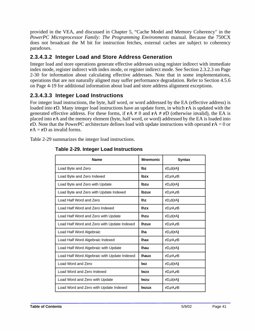
provided in the VEA, and discussed in Chapter 5, “Cache Model and Memory Coherency" in thePowerPC Microprocessor Family: The Programming Environments manual. Because the 750CXdoes not broadcast the M bit for instruction fetches, external caches are subject to coherencyparadoxes.
2.3.4.3.2 Integer Load and Store Address GenerationInteger load and store operations generate effective addresses using register indirect with immediateindex mode, register indirect with index mode, or register indirect mode. See Section 2.3.2.3 on Page2-30 for information about calculating effective addresses. Note that in some implementations,operations that are not naturally aligned may suffer performance degradation. Refer to Section 4.5.6on Page 4-19 for additional information about load and store address alignment exceptions.
2.3.4.3.3 Integer Load InstructionsFor integer load instructions, the byte, half word, or word addressed by the EA (effective address) isloaded into rD. Many integer load instructions have an update form, in which rA is updated with thegenerated effective address. For these forms, if rA ≠ 0 and rA ≠ rD (otherwise invalid), the EA isplaced into rA and the memory element (byte, half word, or word) addressed by the EA is loaded intorD. Note that the PowerPC architecture defines load with update instructions with operand rA = 0 orrA = rD as invalid forms.
Table 2-29 summarizes the integer load instructions.
Table 2-29. Integer Load Instructions
Name Mnemonic Syntax
Load Byte and Zero lbz rD,d(rA)
Load Byte and Zero Indexed lbzx rD,rA,rB
Load Byte and Zero with Update lbzu rD,d(rA)
Load Byte and Zero with Update Indexed lbzux rD,rA,rB
Load Half Word and Zero lhz rD,d(rA)
Load Half Word and Zero Indexed lhzx rD,rA,rB
Load Half Word and Zero with Update lhzu rD,d(rA)
Load Half Word and Zero with Update Indexed lhzux rD,rA,rB
Load Half Word Algebraic lha rD,d(rA)
Load Half Word Algebraic Indexed lhax rD,rA,rB
Load Half Word Algebraic with Update lhau rD,d(rA)
Load Half Word Algebraic with Update Indexed lhaux rD,rA,rB
Load Word and Zero lwz rD,d(rA)
Load Word and Zero Indexed lwzx rD,rA,rB
Load Word and Zero with Update lwzu rD,d(rA)
Load Word and Zero with Update Indexed lwzux rD,rA,rB
Table of Contents 5/9/02 Page 41

Implementation Notes—The following notes describe the 750CX implementation of integer loadinstructions:
• The PowerPC architecture cautions programmers that some implementations of the architecture may execute the load half algebraic (lha, lhax) instructions with greater latency than other types of load instructions. This is not the case for the 750CX; these instructions operate with the same latency as other load instructions.
• The PowerPC architecture cautions programmers that some implementations of the architecture may run the load/store byte-reverse (lhbrx, lbrx, sthbrx, stwbrx) instructions with greater latency than other types of load/store instructions. This is not the case for the 750CX. These instructions operate with the same latency as the other load/store instructions.
• The PowerPC architecture describes some preferred instruction forms for load and store multiple instructions and integer move assist instructions that may perform better than other forms in some implementations. None of these preferred forms affect instruction performance on the 750CX.
• The PowerPC architecture defines the lwarx and stwcx. as a way to update memory atomically. In the 750CX, reservations are made on behalf of aligned 32-byte sections of the memory address space. Executing lwarx and stwcx. to a page marked write-through does not cause a DSI exception if the W bit is set, but as with other memory accesses, DSI exceptions can result for other reasons such as protection violations or page faults.
• In general, because stwcx. always causes an external bus transaction it has slightly worse performance characteristics than normal store operations.
2.3.4.3.4 Integer Store Instructions For integer store instructions, the contents of rS are stored into the byte, half word or word in memoryaddressed by the EA (effective address). Many store instructions have an update form, in which rA isupdated with the EA. For these forms, the following rules apply.
• If rA ≠ 0, the effective address is placed into rA.
• If rS = rA, the contents of register rS are copied to the target memory element, then the generated EA is placed into rA (rS).
The PowerPC architecture defines store with update instructions with rA = 0 as an invalid form. Inaddition, it defines integer store instructions with the CR update option enabled (Rc field, bit 31, inthe instruction encoding = 1) to be an invalid form.
Table 2-30 summarizes the integer store instructions.
Table 2-30. Integer Store Instructions
Name Mnemonic Syntax
Store Byte stb rS,d(rA)
Store Byte Indexed stbx rS,rA,rB
Store Byte with Update stbu rS,d(rA)
Store Byte with Update Indexed stbux rS,rA,rB
Store Half Word sth rS,d(rA)
Page 42 Version 1.1 IBM PowerPC 750CX/750CXe RISC Microprocessor User’s Manual

2.3.4.3.5 Integer Store GatheringThe 750CX performs store gathering for write-through accesses to nonguarded space or tocache-inhibited stores to nonguarded space if the stores are 4 bytes and they are word-aligned. Thesestores are combined in the load/store unit (LSU) to form a double word and are sent out on the 60xbus as a single-beat operation. However, stores can be gathered only if the successive stores that meetthe criteria are queued and pending. Store gathering takes place regardless of the address order of thestores. The store gathering feature is enabled by setting HID0[SGE]. Store gathering is done for bothbig- and little-endian modes.
Store gathering is not done for the following.
• Cacheable stores
• Stores to guarded cache-inhibited or write-through space
• Byte-reverse store
• stwcx. and ecowx accesses
• Floating-point stores
• Store operations attempted during a hardware table search
If store gathering is enabled and the stores do not fall under the above categories, an eieio or syncinstruction must be used to prevent two stores from being gathered.
2.3.4.3.6 Integer Load and Store with Byte-Reverse InstructionsTable 2-31 describes integer load and store with byte-reverse instructions. When used in a PowerPCsystem operating with the default big-endian byte order, these instructions have the effect of loadingand storing data in little-endian order. Likewise, when used in a PowerPC system operating withlittle-endian byte order, these instructions have the effect of loading and storing data in big-endianorder. For more information about big-endian and little-endian byte ordering, see “Byte Ordering" inChapter 3, “Operand Conventions" in the PowerPC Microprocessor Family: The ProgrammingEnvironments manual.
Store Half Word Indexed sthx rS,rA,rB
Store Half Word with Update sthu rS,d(rA)
Store Half Word with Update Indexed sthux rS,rA,rB
Store Word stw rS,d(rA)
Store Word Indexed stwx rS,rA,rB
Store Word with Update stwu rS,d(rA)
Store Word with Update Indexed stwux rS,rA,rB
Table 2-30. Integer Store Instructions (Continued)
Name Mnemonic Syntax
Table of Contents 5/9/02 Page 43

2.3.4.3.7 Integer Load and Store Multiple InstructionsThe load/store multiple instructions are used to move blocks of data to and from the GPRs. The loadmultiple and store multiple instructions may have operands that require memory accesses crossing a4-Kbyte page boundary. As a result, these instructions may be interrupted by a DSI exceptionassociated with the address translation of the second page.
Implementation Notes—The following describes the 750CX implementation of the load/storemultiple instruction.
• For load/store string operations, the hardware does not combine register values to reduce the number of discrete accesses. However, if store gathering is enabled and the accesses fall under the criteria for store gathering the stores may be combined to enhance performance. At a minimum, additional cache access cycles are required.
• The 750CX supports misaligned, single-register load and store accesses in little-endian mode without causing an alignment exception. However, execution of misaligned load/store multiple/string operations causes an alignment exception.
The PowerPC architecture defines the load multiple word (lmw) instruction with rA in the range ofregisters to be loaded as an invalid form.
2.3.4.3.8 Integer Load and Store String InstructionsThe integer load and store string instructions allow movement of data from memory to registers orfrom registers to memory without concern for alignment. These instructions can be used for a shortmove between arbitrary memory locations or to initiate a long move between misaligned memoryfields. However, in some implementations, these instructions are likely to have greater latency andtake longer to execute, perhaps much longer, than a sequence of individual load or store instructionsthat produce the same results.
Table 2-31 summarizes the integer load and store string instructions. In other PowerPCimplementations operating with little-endian byte order, execution of a load or string instruction
Table 2-31. Integer Load and Store with Byte-Reverse Instructions
Name Mnemonic Syntax
Load Half Word Byte-Reverse Indexed lhbrx rD,rA,rB
Load Word Byte-Reverse Indexed lwbrx rD,rA,rB
Store Half Word Byte-Reverse Indexed sthbrx rS,rA,rB
Store Word Byte-Reverse Indexed stwbrx rS,rA,rB
Table 2-32. Integer Load and Store Multiple Instructions
Name Mnemonic Syntax
Load Multiple Word lmw rD,d(rA)
Store Multiple Word stmw rS,d(rA)
Page 44 Version 1.1 IBM PowerPC 750CX/750CXe RISC Microprocessor User’s Manual

invokes the alignment error handler; see “Byte Ordering" in the PowerPC Microprocessor Family:The Programming Environments manual for more information.
Load string and store string instructions may involve operands that are not word-aligned.
As described in Section 4.5.6 on Page 4-19, a misaligned string operation suffers a performancepenalty compared to an aligned operation of the same type.
A non–word-aligned string operation that crosses a 4-Kbyte boundary, or a word-aligned stringoperation that crosses a 256-Mbyte boundary always causes an alignment exception. Anon–word-aligned string operation that crosses a double-word boundary is also slower than aword-aligned string operation.
Implementation Note—The following describes the 750CX implementation of load/store stringinstructions:
• For load/store string operations, the hardware does not combine register values to reduce the number of discrete accesses. However, if store gathering is enabled and the accesses fall under the criteria for store gathering the stores may be combined to enhance performance. At a minimum, additional cache access cycles are required.
• The 750CX supports misaligned, single-register load and store accesses in little-endian mode without causing an alignment exception. However, execution of misaligned load/store multiple/string operations cause an alignment exception.
2.3.4.3.9 Floating-Point Load and Store Address GenerationFloating-point load and store operations generate effective addresses using the register indirect withimmediate index addressing mode and register indirect with index addressing mode. Floating-pointloads and stores are not supported for direct-store accesses. The use of floating-point loads and storesfor direct-store access results in an alignment exception.
Implementation Notes—The 750CX treats exceptions as follows.
• The FPU can be run in two different modes—ignore exceptions mode (MSR[FE0] = MSR[FE1] = 0) and precise mode (any other settings for MSR[FE0,FE1]). For the 750CX, ignore exceptions mode allows floating-point instructions to complete earlier and thus may provide better performance than precise mode.
• The floating-point load and store indexed instructions (lfsx, lfsux, lfdx, lfdux, stfsx, stfsux, stfdx, stfdux) are invalid when the Rc bit is one. In the 750CX, executing one of these invalid instruction forms causes CR0 to be set to an undefined value.
Table 2-33. Integer Load and Store String Instructions
Name Mnemonic Syntax
Load String Word Immediate lswi rD,rA,NB
Load String Word Indexed lswx rD,rA,rB
Store String Word Immediate stswi rS,rA,NB
Store String Word Indexed stswx rS,rA,rB
Table of Contents 5/9/02 Page 45

2.3.4.3.10 Floating-Point Load InstructionsThere are two forms of the floating-point load instruction—single-precision and double-precision.The behavior of double-precision floating-point load instructions, and the behavior ofsingle-precision floating-point load instructions are described here.
Single-precision floating-point load instructions convert single-precision data to double-precisionformat before loading an operand into an FPR.
The PowerPC architecture defines a load with update instruction with rA = 0 as an invalid form.
Table 2-34 summarizes the single- and double-precision floating-point load instructions.
2.3.4.3.11 Floating-Point Store InstructionsThis section describes floating-point store instructions. There are three basic forms of the storeinstruction—single-precision, double-precision, and integer. The integer form is supported by theoptional stfiwx instruction. The behavior of double-precision floating-point store instructions, and thebehavior of single-precision floating-point store instructions are described here. Single-precisionfloating-point store instructions convert double-precision data to single-precision format beforestoring the operands.
Programmers note: After Power-on-reset never store data from the floating-point register file as thefile contains unset data and may have invalid formatted floating-point data. Always initialize thefloating-point register file with valid floating-point data before continuing after a power-on-reset,.
Table 2-35 summarizes the single and double-precision floating-point store and stfiwx instructions.
Table 2-34. Floating-Point Load Instructions
Name Mnemonic Syntax
Load Floating-Point Single lfs frD,d(rA)
Load Floating-Point Single Indexed lfsx frD,rA,rB
Load Floating-Point Single with Update lfsu frD,d(rA)
Load Floating-Point Single with Update Indexed lfsux frD,rA,rB
Load Floating-Point Double lfd frD,d(rA)
Load Floating-Point Double Indexed lfdx frD,rA,rB
Load Floating-Point Double with Update lfdu frD,d(rA)
Load Floating-Point Double with Update Indexed lfdux frD,rA,rB
Page 46 Version 1.1 IBM PowerPC 750CX/750CXe RISC Microprocessor User’s Manual

Some floating-point store instructions require conversions in the LSU.
Table 2-36 shows conversions the LSU makes when executing a Store Floating-Point Singleinstruction.
NOTE: The FPRs are not initialized by HRESET, and they must be initialized with some valid value after POR HRESET and before being stored.
Table 2-35. Floating-Point Store Instructions
Name Mnemonic Syntax
Store Floating-Point Single stfs frS,d(rA)
Store Floating-Point Single Indexed stfsx frS,r B
Store Floating-Point Single with Update stfsu frS,d(rA)
Store Floating-Point Single with Update Indexed stfsux frS,r B
Store Floating-Point Double stfd frS,d(rA)
Store Floating-Point Double Indexed stfdx frS,rB
Store Floating-Point Double with Update stfdu frS,d(rA)
Store Floating-Point Double with Update Indexed stfdux frS,r B
Store Floating-Point as Integer Word Indexed 1 stfiwx frS,rB
Note: 1The stfiwx instruction is optional to the PowerPC architecture.
Table 2-36. Store Floating-Point Single Behavior
FPR Precision Data Type Action
Single Normalized Store
Single Denormalized Store
Single Zero, infinity, QNaN Store
Single SNaN Store
Double Normalized If(exp ð≤ 896)then Denormalize and Storeelse
Store
Double Denormalized Store zero
Double Zero, infinity, QNaN Store
Double SNaN Store
Table of Contents 5/9/02 Page 47

Table 2-37 shows the conversions made when performing a Store Floating-Point Double instruction.Most entries in the table indicate that the floating-point value is simply stored. Only in a few casesare any other actions taken.
Architecturally, all single and double-precision floating-point numbers are represented indouble-precision format within the 750CX. Execution of a store floating-point single (stfs, stfsu,stfsx, stfsux) instruction requires conversion from double to single-precision format. If the exponentis not greater than 896, this conversion requires denormalization. The 750CX supports thisdenormalization by shifting the mantissa one bit at a time. Anywhere from 1 to 23 clock cycles arerequired to complete the denormalization, depending upon the value to be stored.
Because of how floating-point numbers are implemented in the 750CX, there is also a case whenexecution of a store floating-point double (stfd, stfdu, stfdx, stfdux) instruction can require internalshifting of the mantissa. This case occurs when the operand of a store floating-point doubleinstruction is a denormalized single-precision value. The value could be the result of a loadfloating-point single instruction, a single-precision arithmetic instruction, or a floating round tosingle-precision instruction. In these cases, shifting the mantissa takes from 1 to 23 clock cycles,depending upon the value to be stored. These cycles are incurred during the store.
Table 2-37. Store Floating-Point Double Behavior
FPR Precision Data Type Action
Single Normalized Store
Single Denormalized Normalize and Store
Single Zero, infinity, QNaN Store
Single SNaN Store
Double Normalized Store
Double Denormalized Store
Double Zero, infinity, QNaN Store
Double SNaN Store
Page 48 Version 1.1 IBM PowerPC 750CX/750CXe RISC Microprocessor User’s Manual

2.3.4.4 Branch and Flow Control Instructions Some branch instructions can redirect instruction execution conditionally based on the value of bitsin the CR. When the processor encounters one of these instructions, it scans the execution pipelinesto determine whether an instruction in progress may affect the particular CR bit. If no interlock isfound, the branch can be resolved immediately by checking the bit in the CR and taking the actiondefined for the branch instruction.
2.3.4.4.1 Branch Instruction Address Calculation Branch instructions can alter the sequence of instruction execution. Instruction addresses are alwaysassumed to be word aligned; the PowerPC processors ignore the two low-order bits of the generatedbranch target address. Branch instructions compute the EA of the next instruction address using thefollowing addressing modes.
• Branch relative
• Branch conditional to relative address
• Branch to absolute address
• Branch conditional to absolute address
• Branch conditional to link register
• Branch conditional to count register
Note that in 750CX, all branch instructions (b, ba, bl, bla, bc, bca, bcl, bcla, bclr, bclrl, bcctr,bcctrl) and condition register logical instructions (crand, cror, crxor, crnand, crnor, crandc, creqv,crorc, and mcrf) are executed by the BPU. Some of these instructions can redirect instructionexecution conditionally based on the value of bits in the CR. Whenever the CR bits resolve, the branchdirection is either marked as correct or mispredicted. Correcting a mispredicted branch requires thatthe 750CX flush speculatively executed instructions and restore the machine state to immediatelyafter the branch. This correction can be done immediately upon resolution of the condition registersbits.
2.3.4.4.2 Branch Instructions Table 2-38 lists the branch instructions provided by the PowerPC processors. To simplify assemblylanguage programming, a set of simplified mnemonics and symbols is provided for the mostfrequently used forms of branch conditional, compare, trap, rotate and shift, and certain otherinstructions.
See Appendix F, “Simplified Mnemonics" in the PowerPC Microprocessor Family: TheProgramming Environments manual for a list of simplified mnemonic examples.
Table 2-38. Branch Instructions
Name Mnemonic Syntax
Branch b (ba bl bla) target_addr
Branch Conditional bc (bca bcl bcla) BO,BI,target_addr
Branch Conditional to Link Register bclr (bclrl) BO,BI
Branch Conditional to Count Register bcctr (bcctrl) BO,BI
Table of Contents 5/9/02 Page 49

2.3.4.4.3 Condition Register Logical Instructions Condition register logical instructions and the Move Condition Register Field (mcrf) instruction arealso defined as flow control instructions.
Table 2-39 shows these instructions.
NOTE: If the LR update option is enabled for any of these instructions, the PowerPC architecture defines these forms of the instructions as invalid.
2.3.4.4.4 Trap Instructions The trap instructions shown in Table 2-40 are provided to test for a specified set of conditions. If anyof the conditions tested by a trap instruction are met, the system trap type program exception is taken.For more information, see Section 4.5.7 on Page 4-19. If the tested conditions are not met, instructionexecution continues normally.
See Appendix F, “Simplified Mnemonics" in the PowerPC Microprocessor Family: TheProgramming Environments manual for a complete set of simplified mnemonics.
Table 2-39. Condition Register Logical Instructions
Name Mnemonic Syntax
Condition Register AND crand crbD,crbA,crbB
Condition Register OR cror crbD,crbA,crbB
Condition Register XOR crxor crbD,crbA,crbB
Condition Register NAND crnand crbD,crbA,crbB
Condition Register NOR crnor crbD,crbA,crbB
Condition Register Equivalent creqv crbD,crbA, crbB
Condition Register AND with Complement crandc crbD,crbA, crbB
Condition Register OR with Complement crorc crbD,crbA, crbB
Move Condition Register Field mcrf crfD,crfS
Table 2-40. Trap Instructions
Name Mnemonic Syntax
Trap Word Immediate twi TO,rA,SIMM
Trap Word tw TO,rA,rB
Page 50 Version 1.1 IBM PowerPC 750CX/750CXe RISC Microprocessor User’s Manual

2.3.4.5 System Linkage Instruction—UISA The System Call (sc) instruction permits a program to call on the system to perform a service; seeTable 2-41. See also Section 2.3.6.1 on Page 2-60 for additional information.
Executing this instruction causes the system call exception handler to be evoked. For moreinformation, see Section 4.5.10 on Page 4-20.
2.3.4.6 Processor Control Instructions—UISA Processor control instructions are used to read from and write to the condition register (CR), machinestate register (MSR), and special-purpose registers (SPRs).
See Section 2.3.5.1 on Page 2-56 for the mftb instruction and Section 2.3.6.2 on Page 2-61 forinformation about the instructions used for reading from and writing to the MSR and SPRs.
2.3.4.6.1 Move to/from Condition Register Instructions Table 2-42 summarizes the instructions for reading from or writing to the condition register.
Implementation Note—The PowerPC architecture indicates that in some implementations the Moveto Condition Register Fields (mtcrf) instruction may perform more slowly when only a portion of thefields are updated as opposed to all of the fields. The condition register access latency for 750CX isthe same in both cases.
2.3.4.6.2 Move to/from Special-Purpose Register Instructions (UISA) Table 2-43 lists the mtspr and mfspr instructions.
Table 2-41. System Linkage Instruction—UISA
Name Mnemonic Syntax
System Call sc —
Table 2-42. Move to/from Condition Register Instructions
Name Mnemonic Syntax
Move to Condition Register Fields mtcrf CRM,rS
Move to Condition Register from XER mcrxr crfD
Move from Condition Register mfcr rD
Table 2-43. Move to/from Special-Purpose Register Instructions (UISA)
Name Mnemonic Syntax
Move to Special-Purpose Register mtspr SPR,rS
Move from Special-Purpose Register mfspr rD,SPR
Table of Contents 5/9/02 Page 51

Table 2-44 lists the SPR numbers for both user and supervisor-level accesses.
Table 2-44. PowerPC Encodings
Register NameSPR
1
Access mfspr/mtsprDecimal spr[5–9] spr[0–4]
CTR 9 00000 01001 User (UISA) Both
DABR 1013 11111 10101 Supervisor (OEA) Both
DAR 19 00000 10011 Supervisor (OEA) Both
DBAT0L 537 10000 11001 Supervisor (OEA) Both
DBAT0U 536 10000 11000 Supervisor (OEA) Both
DBAT1L 539 10000 11011 Supervisor (OEA) Both
DBAT1U 538 10000 11010 Supervisor (OEA) Both
DBAT2L 541 10000 11101 Supervisor (OEA) Both
DBAT2U 540 10000 11100 Supervisor (OEA) Both
DBAT3L 543 10000 11111 Supervisor (OEA) Both
DBAT3U 542 10000 11110 Supervisor (OEA) Both
DEC 22 00000 10110 Supervisor (OEA) Both
DSISR 18 00000 10010 Supervisor (OEA) Both
EAR 282 01000 11010 Supervisor (OEA) Both
IBAT0L 529 10000 10001 Supervisor (OEA) Both
IBAT0U 528 10000 10000 Supervisor (OEA) Both
IBAT1L 531 10000 10011 Supervisor (OEA) Both
IBAT1U 530 10000 10010 Supervisor (OEA) Both
IBAT2L 533 10000 10101 Supervisor (OEA) Both
IBAT2U 532 10000 10100 Supervisor (OEA) Both
IBAT3L 535 10000 10111 Supervisor (OEA) Both
IBAT3U 534 10000 10110 Supervisor (OEA) Both
LR 8 00000 01000 User (UISA) Both
PVR 287 01000 11111 Supervisor (OEA) mfspr
SDR1 25 00000 11001 Supervisor (OEA) Both
SPRG0 272 01000 10000 Supervisor (OEA) Both
SPRG1 273 01000 10001 Supervisor (OEA) Both
SPRG2 274 01000 10010 Supervisor (OEA) Both
SPRG3 275 01000 10011 Supervisor (OEA) Both
Page 52 Version 1.1 IBM PowerPC 750CX/750CXe RISC Microprocessor User’s Manual

Encodings for the 750CX-specific SPRs are listed in Table 2-45.
SRR0 26 00000 11010 Supervisor (OEA) Both
SRR1 27 00000 11011 Supervisor (OEA) Both
TBL 2 268 01000 01100 User (VEA) mfspr
284 01000 11100 Supervisor (OEA) mtspr
TBU 2 269 01000 01101 User (VEA) mfspr
285 01000 11101 Supervisor (OEA) mtspr
XER 1 00000 00001 User (UISA) Both
Notes: 1 The order of the two 5-bit halves of the SPR number is reversed compared with actual
instruction coding. For mtspr and mfspr instructions, the SPR number coded in assembly language does not appear directly as a 10-bit binary number in the instruction. The number coded is split into two 5-bit halves that are reversed in the instruction, with the high-order five bits appearing in bits 16–20 of the instruction and the low-order five bits in bits 11–15.
2 The TB registers are referred to as TBRs rather than SPRs and can be written to using the mtspr instruction in supervisor mode and the TBR numbers here. The TB registers can be read in user mode using either the mftb or mfspr instruction and specifying TBR 268 for TBL and SPR 269 for TBU.
Table 2-45. SPR Encodings for 750CX-Defined Registers (mfspr)
Register Name
SPR1
Access mfspr/mtsprDecimal spr[5–9] spr[0–4]
DABR 1013 11111 10101 User Both
HID0 1008 11111 10000 Supervisor Both
HID1 1009 11111 10001 Supervisor Both
IABR 1010 11111 10010 Supervisor Both
ICTC 1019 11111 11011 Supervisor Both
L2CR 1017 11111 11001 Supervisor Both
MMCR0 952 11101 11000 Supervisor Both
MMCR1 956 11101 11100 Supervisor Both
PMC1 953 11101 11001 Supervisor Both
PMC2 954 11101 11010 Supervisor Both
Table 2-44. PowerPC Encodings (Continued)
Register NameSPR
1
Access mfspr/mtsprDecimal spr[5–9] spr[0–4]
Table of Contents 5/9/02 Page 53

2.3.4.7 Memory Synchronization Instructions—UISA Memory synchronization instructions control the order in which memory operations are completedwith respect to asynchronous events, and the order in which memory operations are seen by otherprocessors or memory access mechanisms. See Chapter 3, "The 750CX Instruction and Data Cache
PMC3 957 11101 11101 Supervisor Both
PMC4 958 11101 11110 Supervisor Both
SIA 955 11101 11011 Supervisor Both
THRM1 1020 11111 11100 Supervisor Both
THRM2 1021 11111 11101 Supervisor Both
THRM3 1022 11111 11110 Supervisor Both
UMMCR0 936 11101 01000 User mfspr
UMMCR1 940 11101 01100 User mfspr
UPMC1 937 11101 01001 User mfspr
UPMC2 938 11101 01010 User mfspr
UPMC3 941 11101 01101 User mfspr
UPMC4 942 11101 01110 User mfspr
USIA 939 11101 01011 User mfspr
Note: 1Note that the order of the two 5-bit halves of the SPR number is reversed compared with actual instruction coding.
For mtspr and mfspr instructions, the SPR number coded in assembly language does not appear directly as a 10-bit binary number in the instruction. The number coded is split into two 5-bit halves that are reversed in the instruction, with the high-order 5 bits appearing in bits 16–20 of the instruction and the low-order 5 bits in bits 11–15.
Table 2-45. SPR Encodings for 750CX-Defined Registers (mfspr) (Continued)
Register Name
SPR1
Access mfspr/mtsprDecimal spr[5–9] spr[0–4]
Page 54 Version 1.1 IBM PowerPC 750CX/750CXe RISC Microprocessor User’s Manual

Operation" for additional information about these instructions and about related aspects of memorysynchronization. See Table 2-46 for a summary.
System designs with an L2 cache should take special care to recognize the hardware signaling causedby a SYNC bus operation and perform the appropriate actions to guarantee that memory referencesthat may be queued internally to the L2 cache have been performed globally.
See 2.3.5.2, “Memory Synchronization Instructions—VEA" for details about additional memorysynchronization (eieio and isync) instructions.
In the PowerPC architecture, the Rc bit must be zero for most load and store instructions. If Rc is set,the instruction form is invalid for sync and lwarx instructions. If the 750CX encounters one of theseinvalid instruction forms, it sets CR0 to an undefined value.
2.3.5 PowerPC VEA Instructions The PowerPC virtual environment architecture (VEA) describes the semantics of the memory modelthat can be assumed by software processes, and includes descriptions of the cache model, cachecontrol instructions, address aliasing, and other related issues. Implementations that conform to theVEA also adhere to the UISA, but may not necessarily adhere to the OEA.
This section describes additional instructions that are provided by the VEA.
Table 2-46. Memory Synchronization Instructions—UISA
Name Mnemonic Syntax Implementation Notes
Load Word and Reserve Indexed
lwarx rD,rA,rB Programmers can use lwarx with stwcx. to emulate common semaphore operations such as test and set, compare and swap, exchange memory, and fetch and add. Both instructions must use the same EA. Reservation granularity is implementation-dependent. 750CX makes reservations on behalf of aligned 32-byte sections of the memory address space. If the W bit is set, executing lwarx and stwcx. to a page marked write-through does not cause a DSI exception, but DSI exceptions can result for other reasons. If the location is not word-aligned, an alignment exception occurs. The stwcx. instruction is the only load/store instruction with a valid form if Rc is set. If Rc is zero, executing stwcx. sets CR0 to an undefined value. In general, stwcx. always causes a transaction on the external bus and thus operates with slightly worse performance characteristics than normal store operations.
Store Word Conditional Indexed
stwcx. rS,rA,rB
Synchronize sync — Because it delays subsequent instructions until all previous instructions complete to where they cannot cause an exception, sync is a barrier against store gathering. Additionally, all load/store cache/bus activities initiated by prior instructions are completed. Touch load operations (dcbt, dcbtst) must complete address translation, but need not complete on the bus. If HID0[ABE] = 1, sync completes after a successful broadcast. The latency of sync depends on the processor state when it is dispatched and on various system-level situations. Therefore, frequent use of sync may degrade performance.
Table of Contents 5/9/02 Page 55

2.3.5.1 Processor Control Instructions—VEA In addition to the move to condition register instructions (specified by the UISA), the VEA definesthe mftb instruction (user-level instruction) for reading the contents of the time base register; seeChapter 3, "The 750CX Instruction and Data Cache Operation" for more information.
Table 2-47 shows the mftb instruction.
Simplified mnemonics are provided for the mftb instruction so it can be coded with the TBR nameas part of the mnemonic rather than requiring it to be coded as an operand. See Appendix F,“Simplified Mnemonics" in the PowerPC Microprocessor Family: The Programming Environmentsmanual for simplified mnemonic examples and for simplified mnemonics for Move from Time Base(mftb) and Move from Time Base Upper (mftbu), which are variants of the mftb instruction ratherthan of mfspr. The mftb instruction serves as both a basic and simplified mnemonic. Assemblersrecognize an mftb mnemonic with two operands as the basic form, and an mftb mnemonic with oneoperand as the simplified form. Note that 750CX ignores the extended opcode differences betweenmftb and mfspr by ignoring bit 25 and treating both instructions identically.
Implementation Notes—The following information is useful with respect to using the time baseimplementation in the 750CX:
• The 750CX allows user-mode read access to the time base counter through the use of the Move from Time Base (mftb) and the Move from Time Base Upper (mftbu) instructions. As a 32-bit PowerPC implementation, the 750CX can access TBU and TBL only separately, whereas 64-bit implementations can access the entire TB register at once.
• The time base counter is clocked at a frequency that is one-fourth that of the bus clock.
2.3.5.2 Memory Synchronization Instructions—VEA Memory synchronization instructions control the order in which memory operations are completedwith respect to asynchronous events, and the order in which memory operations are seen by otherprocessors or memory access mechanisms. See Chapter 3, "The 750CX Instruction and Data CacheOperation" for more information about these instructions and about related aspects of memorysynchronization.
In addition to the sync instruction (specified by UISA), the VEA defines the Enforce In-OrderExecution of I/O (eieio) and Instruction Synchronize (isync) instructions. The number of cyclesrequired to complete an eieio instruction depends on system parameters and on the processor's statewhen the instruction is issued. As a result, frequent use of this instruction may degrade performanceslightly.
Table 2-47. Move from Time Base Instruction
Name Mnemonic Syntax
Move from Time Base mftb rD, TBR
Page 56 Version 1.1 IBM PowerPC 750CX/750CXe RISC Microprocessor User’s Manual

Table 2-48 describes the memory synchronization instructions defined by the VEA.
2.3.5.3 Memory Control Instructions—VEA Memory control instructions can be classified as follows:
• Cache management instructions (user-level and supervisor-level)
• Segment register manipulation instructions (OEA)
• Translation lookaside buffer management instructions (OEA)
This section describes the user-level cache management instructions defined by the VEA. See Section2.3.6.3 on Page 2-61 for information about supervisor-level cache, segment register manipulation,and translation lookaside buffer management instructions.
2.3.5.3.1 User-Level Cache Instructions—VEA The instructions summarized in this section help user-level programs manage on-chip caches if theyare implemented. See Chapter 3, "The 750CX Instruction and Data Cache Operation" for moreinformation about cache topics. The following sections describe how these operations are treated withrespect to the 750CX’s cache.
As with other memory-related instructions, the effects of cache management instructions on memoryare weakly-ordered. If the programmer must ensure that cache or other instructions have beenperformed with respect to all other processors and system mechanisms, a sync instruction must beplaced after those instructions.
Note that the 750CX interprets cache control instructions (icbi, dcbi, dcbf, dcbz, and dcbst) as if theypertain only to the local L1 and L2 cache. A dcbz (with M set) is always broadcast on the 60x bus.The dcbi, dcbf, and dcbst operations are broadcast if HID0[ABE] is set.
Table 2-48. Memory Synchronization Instructions—VEA
Name Mnemonic Syntax Implementation Notes
Enforce In-Order Execution of I/O
eieio — The eieio instruction is dispatched to the LSU and executes after all previous cache-inhibited or write-through accesses are performed; all subsequent instructions that generate such accesses execute after eieio. If HID0[ABE] = 1 an EIEIO operation is broadcast on the external bus to enforce ordering in the external memory system. The eieio operation bypasses the L2 cache and is forwarded to the bus unit. If HID0[ABE] = 0, the operation is not broadcast.Because the 750CX does not reorder noncacheable accesses, eieio is not needed to force ordering. However, if store gathering is enabled and an eieio is detected in a store queue, stores are not gathered. If HID0[ABE] = 1, broadcasting eieio prevents external devices, such as a bus bridge chip, from gathering stores. .
Instruction Synchronize
isync — The isync instruction is refetch serializing; that is, it causes the 750CX to purge its instruction queue and wait for all prior instructions to complete before refetching the next instruction, which is not executed until all previous instructions complete to the point where they cannot cause an exception. The isync instruction does not wait for all pending stores in the store queue to complete. Any instruction after an isync sees all effects of prior instructions.
Table of Contents 5/9/02 Page 57

The 750CX never broadcasts an icbi. Of the broadcast cache operations, the 750CX snoops onlydcbz, regardless of the HID0[ABE] setting. Any bus activity caused by other cache instructionsresults directly from performing the operation on the 750CX cache. All cache control instructions toT = 1 space are no-ops. For information on how cache control instructions affect the L2, seeChapter 9, "L2 Cache".
Table 2-49 summarizes the cache instructions defined by the VEA. Note that these instructions areaccessible to user-level programs.
Table 2-49. User-Level Cache Instructions
Name Mnemonic Syntax Implementation Notes
Data Cache Block Touch 1
dcbt rA,rB The VEA defines this instruction to allow for potential system performance enhancements through the use of software-initiated prefetch hints. Implementations are not required to take any action based on execution of this instruction, but they may prefetch the cache block corresponding to the EA into their cache. When dcbt executes, the 750CX checks for protection violations (as for a load instruction). This instruction is treated as a no-op for the following cases:• A valid translation is not found either in BAT or TLB• The access causes a protection violation.• The page is mapped cache-inhibited, G = 1 (guarded), or T = 1.• The cache is locked or disabled• HID0[NOOPTI] = 1Otherwise, if no data is in the cache location, the 750CX requests a cache line fill (with intent to modify). Data brought into the cache is validated as if it were a load instruction. The memory reference of a dcbt sets the reference bit.
Data Cache Block Touch for Store 1
dcbtst rA,rB This instruction behaves like dcbt.
Data Cache Block Set to Zero
dcbz rA,rB The EA is computed, translated, and checked for protection violations. For cache hits, four beats of zeros are written to the cache block and the tag is marked M. For cache misses with the replacement block marked E, the zero line fill is performed and the cache block is marked M. However, if the replacement block is marked M, the contents are written back to memory first. The instruction executes regardless of whether the cache is locked; if the cache is disabled, an alignment exception occurs. If M = 1 (coherency enforced), the address is broadcast to the bus before the zero line fill.The exception priorities (from highest to lowest) are as follows:1 Cache disabled—Alignment exception 2 Page marked write-through or cache Inhibited—Alignment exception3 BAT protection violation—DSI exception4 TLB protection violation—DSI exceptiondcbz is the only cache instruction that broadcasts even if HID0[ABE] = 0.
Page 58 Version 1.1 IBM PowerPC 750CX/750CXe RISC Microprocessor User’s Manual

2.3.5.4 Optional External Control Instructions The PowerPC architecture defines an optional external control feature that, if implemented, issupported by the two external control instructions, eciwx and ecowx. These instructions allow auser-level program to communicate with a special-purpose device. These instructions are providedand are summarized in Table 2-50.
Data Cache Block Store
dcbst rA,rB The EA is computed, translated, and checked for protection violations. • For cache hits with the tag marked E, no further action is taken. • For cache hits with the tag marked M, the cache block is written back
to memory and marked E. A dcbst is not broadcast unless HID0[ABE] = 1 regardless of WIMG settings. The instruction acts like a load with respect to address translation and memory protection. It executes regardless of whether the cache is disabled or locked. The exception priorities (from highest to lowest) for dcbst are as follows:1 BAT protection violation—DSI exception2 TLB protection violation—DSI exception.
Data Cache Block Flush
dcbf rA,rB The EA is computed, translated, and checked for protection violations. • For cache hits with the tag marked M, the cache block is written back
to memory and the cache entry is invalidated. • For cache hits with the tag marked E, the entry is invalidated. • For cache misses, no further action is taken. A dcbf is not broadcast unless HID0[ABE] = 1 regardless of WIMG settings. The instruction acts like a load with respect to address translation and memory protection. It executes regardless of whether the cache is disabled or locked. The exception priorities (from highest to lowest) for dcbf are as follows:1 BAT protection violation—DSI exception2 TLB protection violation—DSI exception.
Instruction Cache Block Invalidate
icbi rA,rB This instruction performs a virtual lookup into the instruction cache (index only). The address is not translated, so it cannot cause an exception. All ways of a selected set are invalidated regardless of whether the cache is disabled or locked. The 750CX never broadcasts icbi onto the 60x bus.
Note:1 A program that uses dcbt and dcbtst instructions improperly performs less efficiently. To improve performance, HID0[NOOPTI] may be set, which causes dcbt and dcbtst to be no-oped at the cache. They do not cause bus activity and cause only a 1-clock execution latency. The default state of this bit is zero which enables the use of these instructions.
Table 2-49. User-Level Cache Instructions (Continued)
Name Mnemonic Syntax Implementation Notes
Table of Contents 5/9/02 Page 59

The eciwx/ecowx instructions let a system designer map special devices in an alternative way. TheMMU translation of the EA is not used to select the special device, as it is used in most instructionssuch as loads and stores. Rather, it is used as an address operand that is passed to the device over theaddress bus. Four other signals (the burst and size signals on the 60x bus) are used to select the device;these four signals output the 4-bit resource ID (RID) field located in the EAR. The eciwx instructionalso loads a word from the data bus that is output by the special device. For more information aboutthe relationship between these instructions and the system interface, refer to Chapter 7, "SignalDescriptions".
2.3.6 PowerPC OEA Instructions The PowerPC operating environment architecture (OEA) includes the structure of the memorymanagement model, supervisor-level registers, and the exception model. Implementations thatconform to the OEA also adhere to the UISA and the VEA. This section describes the instructionsprovided by the OEA.
2.3.6.1 System Linkage Instructions—OEA This section describes the system linkage instructions (see Table 2-51). The user-level sc instructionlets a user program call on the system to perform a service and causes the processor to take a systemcall exception. The supervisor-level rfi instruction is used for returning from an exception handler.
Table 2-50. External Control Instructions
Name Mnemonic Syntax Implementation Notes
External Control In Word Indexed
eciwx rD,rA,rB A transfer size of 4 bytes is implied; the TBST and TSIZ[0–2] signals are redefined to specify the Resource ID (RID), copied from bits EAR[28–31]. For these operations, TBST carries the EAR[28] data. Misaligned operands for these instructions cause an alignment exception. Addressing a location where SR[T] = 1 causes a DSI exception. If MSR[DR] = 0 a programming error occurs and the physical address on the bus is undefined. Note: These instructions are optional to the PowerPC architecture.
External Control Out Word Indexed
ecowx rS,rA,rB
Table 2-51. System Linkage Instructions—OEA
Name Mnemonic Syntax Implementation Notes
System Call sc — The sc instruction is context-synchronizing.
Return from Interrupt
rfi — The rfi instruction is context-synchronizing. For the 750CX, this means the rfi instruction works its way to the final stage of the execution pipeline, updates architected registers, and redirects the instruction flow.
Page 60 Version 1.1 IBM PowerPC 750CX/750CXe RISC Microprocessor User’s Manual

2.3.6.2 Processor Control Instructions—OEA This section describes the processor control instructions used to access the MSR and the SPRs.Table 2-52 lists instructions for accessing the MSR.
The OEA defines encodings of mtspr and mfspr to provide access to supervisor-level registers. Theinstructions are listed in Table 2-53.
Encodings for the architecture-defined SPRs are listed in Table 2-44 on Page 2-52. Encodings for750CX-specific, supervisor-level SPRs are listed in Table 2-45 on Page 2-53. Simplified mnemonicsare provided for mtspr and mfspr in Appendix F, “Simplified Mnemonics" in the PowerPCMicroprocessor Family: The Programming Environments manual.
For a discussion of context synchronization requirements when altering certain SPRs, refer toAppendix E, “Synchronization Programming Examples" in the PowerPC Microprocessor Family:The Programming Environments manual.
2.3.6.3 Memory Control Instructions—OEA Memory control instructions include the following.
• Cache management instructions (supervisor-level and user-level).
• Segment register manipulation instructions.
• Translation lookaside buffer management instructions.
This section describes supervisor-level memory control instructions. Section 2.3.5.3 on Page 2-57describes user-level memory control instructions.
Table 2-52. Move to/from Machine State Register Instructions
Name Mnemonic Syntax
Move to Machine State Register mtmsr rS
Move from Machine State Register mfmsr rD
Table 2-53. Move to/from Special-Purpose Register Instructions (OEA)
Name Mnemonic Syntax
Move to Special-Purpose Register mtspr SPR,rS
Move from Special-Purpose Register mfspr rD,SPR
Table of Contents 5/9/02 Page 61

2.3.6.3.1 Supervisor-Level Cache Management Instruction—(OEA)Table 2-54 lists the only supervisor-level cache management instruction.
See Section 2.3.5.3.1 on Page 2-57 for cache instructions that provide user-level programs the abilityto manage the on-chip caches. If the effective address references a direct-store segment, theinstruction is treated as a no-op.
2.3.6.3.2 Segment Register Manipulation Instructions (OEA)The instructions listed in Table 2-55 provide access to the segment registers for 32-bitimplementations. These instructions operate completely independently of the MSR[IR] andMSR[DR] bit settings. Refer to “Synchronization Requirements for Special Registers and forLookaside Buffers" in Chapter 2, “PowerPC Register Set" of the PowerPC Microprocessor Family:The Programming Environments manual for serialization requirements and other recommendedprecautions to observe when manipulating the segment registers. Be sure to execute an isync afterexecution of a mtsr instruction.
Table 2-54. Supervisor-Level Cache Management Instruction
Name Mnemonic Syntax Implementation Notes
Data Cache Block Invalidate
dcbi rA,rB The EA is computed, translated, and checked for protection violations. For cache hits, the cache block is marked I regardless of whether it was marked E or M. A dcbi is not broadcast unless HID0[ABE] = 1, regardless of WIMG settings. The instruction acts like a store with respect to address translation and memory protection. It executes regardless of whether the cache is disabled or locked. The exception priorities (from highest to lowest) for dcbi are as follows:1 BAT protection violation—DSI exception 2 TLB protection violation—DSI exception.
Table 2-55. Segment Register Manipulation Instructions
Name Mnemonic Syntax Implementation Notes
Move to Segment Register mtsr SR,rS —execute isync after mtsr
Move to Segment Register Indirect mtsrin rS,rB —execute isync after mtsrin
Move from Segment Register mfsr rD,SR The shadow SRs in the instruction MMU can be read by setting HID0[RISEG] before executing mfsr.
Move from Segment Register Indirect mfsrin rD,rB —
Page 62 Version 1.1 IBM PowerPC 750CX/750CXe RISC Microprocessor User’s Manual

2.3.6.3.3 Translation Lookaside Buffer Management Instructions—(OEA)The address translation mechanism is defined in terms of the segment descriptors and page tableentries (PTEs) PowerPC processors use to locate the logical-to-physical address mapping for aparticular access. These segment descriptors and PTEs reside in segment registers and page tables inmemory, respectively.
See Chapter 7, "Signal Descriptions" for more information about TLB operations.
Table 2-56 summarizes the operation of the TLB instructions in the 750CX.
Implementation Note—The tlbia instruction is optional for an implementation if its effects can beachieved through some other mechanism. Therefore, it is not implemented on the 750CX. Asdescribed above, tlbie can be used to invalidate a particular index of the TLB based on EA[14–19]—asequence of 64 tlbie instructions followed by a tlbsync instruction invalidates all the TLB structures(for EA[14–19] = 0, 1, 2,..., 63). Attempting to execute tlbia causes an illegal instruction programexception.
The presence and exact semantics of the TLB management instructions areimplementation-dependent. To minimize compatibility problems, system software should incorporateuses of these instructions into subroutines.
2.3.7 Recommended Simplified Mnemonics To simplify assembly language coding, a set of alternative mnemonics is provided for somefrequently used operations (such as no-op, load immediate, load address, move register, andcomplement register). Programs written to be portable across the various assemblers for the PowerPCarchitecture should not assume the existence of mnemonics not described in this document.
For a complete list of simplified mnemonics, see Appendix F, “Simplified Mnemonics" in thePowerPC Microprocessor Family: The Programming Environments manual.
Table 2-56. Translation Lookaside Buffer Management Instruction
Name Mnemonic Syntax Implementation Notes
TLB Invalidate Entry
tlbie rB Invalidates both ways in both instruction and data TLB entries at the index provided by EA[14–19]. It executes regardless of the MSR[DR] and MSR[IR] settings.To invalidate all entries in both TLBs, the programmer should issue 64 tlbie instructions that each successively increment this field.
TLB Synchronize
tlbsync — On the 750CX, the only function tlbsync serves is to wait for the TLBISYNC signal to go inactive.
Table of Contents 5/9/02 Page 63

Page 64 Version 1.1 IBM PowerPC 750CX/750CXe RISC Microprocessor User’s Manual

Chapter 3 The 750CX Instruction and Data Cache Operation
3030
The 750CX microprocessor contains separate 32-Kbyte, eight-way set associative instruction anddata caches to allow the execution units and registers rapid access to instructions and data. Thischapter describes the organization of the on-chip instruction and data caches, the MEI cachecoherency protocol, cache control instructions, various cache operations, and the interaction betweenthe caches, the load/store unit (LSU), the instruction unit, and the bus interface unit (BIU).
Note that in this chapter, the term ‘multiprocessor’ is used in the context of maintaining cachecoherency. These multiprocessor devices could be actual processors or other devices that can accesssystem memory, maintain their own caches, and function as bus masters requiring cache coherency.If the L2 cache is enabled, read Chapter 9, "L2 Cache" before reading this chapter.
The 750CX L1 cache implementation has the following characteristics.
• There are two separate 32-Kbyte instruction and data caches (Harvard architecture).
• Both instruction and data caches are eight-way set associative.
• The caches implement a pseudo least-recently-used (PLRU) replacement algorithm within each set.
• The cache directories are physically addressed. The physical (real) address tag is stored in the cache directory.
• Both the instruction and data caches have 32-byte cache blocks. A cache block is the block of memory that a coherency state describes, also referred to as a cache line.
• Two coherency state bits for each data cache block allow encoding for three states:
— Modified (Exclusive) (M)
— Exclusive (Unmodified) (E)
— Invalid (I)
• A single coherency state bit for each instruction cache block allows encoding for two possible states:
— Invalid (INV)
— Valid (VAL)
• Each cache can be invalidated or locked by setting the appropriate bits in the hardware implementation-dependent register 0 (HID0), a special-purpose register (SPR) specific to the 750CX.
The 750CX supports a fully-coherent 4-Gbyte physical memory address space. Bus snooping is usedto drive the MEI three-state cache coherency protocol that ensures the coherency of global memorywith respect to the processor’s data cache. The MEI protocol is described in Section 3.3.2 on Page 3-7.
On a cache miss, the 750CX’s cache blocks are filled in four beats of 64 bits each. The burst fill isperformed as a critical-double-word-first operation; the critical double word is simultaneously writtento the cache and forwarded to the requesting unit, thus minimizing stalls due to cache fill latency. Thedata cache line is first loaded into a 32-byte re-load buffer and when it is full, it is written into the data
Table of Contents 5/9/02 Page 1

cache in one cycle. This minimizes the contention between load-store unit and the line reloadfunction. See Figure 9-1 on Page 9-2.
The instruction and data caches are integrated into the 750CX as shown in Figure 3-1.
Figure 3-1. Cache Integration
Both caches are tightly coupled into the 750CX’s bus interface unit to allow efficient access to thesystem memory controller and other bus masters. The bus interface unit receives requests for busoperations from the instruction and data caches, and executes the operations per the 60x bus protocol.The BIU provides address queues, prioritizing logic, and bus control logic. The BIU captures snoopaddresses for data cache, address queue, and memory reservation (lwarx and stwcx. instruction)operations. In the 750CX a L1 cache miss first accesses the L2 cache to find the desired cache blockbefore accessing the BIU.
The data cache provides buffers for load and store bus operations. All the data for the correspondingaddress queues (load and store data queues) is located in the data cache. The data queues areconsidered temporary storage for the cache and not part of the BIU. The data cache also providesstorage for the cache tags required for memory coherency and performs the cache block replacementPLRU function. The data cache is supported by two cache block re-load/write-back buffers. Thisallows a cache block to be loaded or unloaded from the cache in a single cycle. See Figure 9-1 onPage 9-2.
The data cache supplies data to the GPRs and FPRs by means of the load/store unit. The 750CX’sLSU is directly coupled to the data cache to allow efficient movement of data to and from thegeneral-purpose and floating-point registers. The load/store unit provides all logic required tocalculate effective addresses, handles data alignment to and from the data cache, and providessequencing for load and store string and multiple operations. Write operations to the data cache canbe performed on a byte, half-word, word, or double-word basis.
The instruction cache provides a 128-bit interface to the instruction unit, so four instructions can bemade available to the instruction unit in a single clock cycle. The instruction unit accesses the
Instruction UnitLoad/Store Unit
Cache Tags
(LSU)
Instructions (0–127)
Instructions (0–63)
I-Cache32-Kbyte
8-Way Set Associative
Cache Logic
EA (20–26)
PA (0–19)
PA (0–31)
Cache Tags
Cache Logic
D-Cache
32-Kbyte8-Way Set Associative
Data (0–63)
Data (0–63)
EA: Effective AddressPA: Physical Address
MMU/L2/60x BIU
Page 2 Version 1.1 IBM PowerPC 750CX/750CXe RISC Microprocessor User’s Manual

instruction cache frequently in order to sustain the high throughput provided by the six-entryinstruction queue.
3.1 Data Cache OrganizationThe data cache is organized as 128 sets of eight ways as shown in Figure 3-2. Each way consists of32 bytes, two state bits, and an address tag. Note that in the PowerPC architecture, the term ‘cacheblock,’ or simply ‘block,’ when used in the context of cache implementations, refers to the unit ofmemory at which coherency is maintained. For the 750CX, this is the eight-word (32 byte) cache line.This value may be different for other PowerPC implementations.
Each cache block contains eight contiguous words from memory that are loaded from an eight-wordboundary (that is, bits A[27–31] of the logical (effective) addresses are zero); as a result, cache blocksare aligned with page boundaries. Note that address bits A[20–26] provide the index to select a cacheset. Bits A[27–31] select a byte within a block. The two state bits implement a three-state MEI(modified/exclusive/invalid) protocol, a coherent subset of the standard four-state MESI(modified/exclusive/shared/invalid) protocol. The MEI protocol is described in Section 3.3.2. Thetags consist of bits PA[0–19]. Address translation occurs in parallel with set selection (fromA[20–26]), and the higher-order address bits (the tag bits in the cache) are physical.
The 750CX’s on-chip data cache tags are single-ported, and load or store operations must bearbitrated with snoop accesses to the data cache tags. Load or store operations can be performed tothe cache on the clock cycle immediately following a snoop access if the snoop misses; snoop hitsmay block the data cache for two or more cycles, depending on whether a copy-back to main memoryis required.
Figure 3-2. Data Cache Organization
8 Words/Block
128 Sets
Way 5
Way 6
Way 7
Way 4 Address Tag 4
Address Tag 5
Address Tag 6
Address Tag 7
Way 1
Way 2
Way 3
Way 0 Address Tag 0
Address Tag 1
Address Tag 2
Address Tag 3
State
State
State
Words [0–7]
State
Words [0–7]
Words [0–7]
Words [0–7]
State
State
State
Words [0–7]
State
Words [0–7]
Words [0–7]
Words [0–7]
Table of Contents 5/9/02 Page 3

3.2 Instruction Cache OrganizationThe instruction cache also consists of 128 sets of eight ways, as shown in Figure 3-3 on Page 3-5.Each way consists of 32 bytes, a single state bit, and an address tag. As with the data cache, eachinstruction cache block contains eight contiguous words from memory that are loaded from aneight-word boundary (that is, bits A[27–31] of the logical (effective) addresses are zero); as a result,cache blocks are aligned with page boundaries. Also, address bits A[20–26] provide the index toselect a set, and bits A[27–29] select a word within a block.
The tags consist of bits PA[0–19]. Address translation occurs in parallel with set selection (fromA[20–26]), and the higher order address bits (the tag bits in the cache) are physical.
The instruction cache differs from the data cache in that it does not implement MEI cache coherencyprotocol, and a single state bit is implemented that indicates only whether a cache block is valid orinvalid. The instruction cache is not snooped, so if a processor modifies a memory location that maybe contained in the instruction cache, software must ensure that such memory updates are visible tothe instruction fetching mechanism. This can be achieved with the following instruction sequence:
dcbst # update memorysync # wait for updateicbi # remove (invalidate) copy in instruction cachesync # wait for ICBI operation to be globally performedisync # remove copy in own instruction buffer
These operations are necessary because the processor does not maintain instruction memory coherentwith data memory. Software is responsible for enforcing coherency of instruction caches and datamemory.
Since instruction fetching may bypass the data cache, changes made to items in the data cache maynot be reflected in memory until after the instruction fetch completes.
Page 4 Version 1.1 IBM PowerPC 750CX/750CXe RISC Microprocessor User’s Manual

Figure 3-3. Instruction Cache Organization
3.3 Memory and Cache CoherencyThe primary objective of a coherent memory system is to provide the same image of memory to alldevices using the system. Coherency allows synchronization and cooperative use of shared resources.Otherwise, multiple copies of a memory location, some containing stale values, could exist in asystem resulting in errors when the stale values are used. Each potential bus master must follow rulesfor managing the state of its cache. This section describes the coherency mechanisms of the PowerPCarchitecture and the three-state cache coherency protocol of the 750CX’s data cache.
Note that unless specifically noted, the discussion of coherency in this section applies to the 750CX’sdata cache only. The instruction cache is not snooped. Instruction cache coherency must bemaintained by software. However, the 750CX does support a fast instruction cache invalidatecapability as described in Section 3.4.1.4.
8 Words/Block
128 Sets
Way 5
Way 6
Way 7
Way 4 Address Tag 4
Address Tag 5
Address Tag 6
Address Tag 7
Way 1
Way 2
Way 3
Way 0 Address Tag 0
Address Tag 1
Address Tag 2
Address Tag 3
Valid
Valid
Valid
Words [0–7]
Valid
Words [0–7]
Words [0–7]
Words [0–7]
Valid
Valid
Valid
Words [0–7]
Valid
Words [0–7]
Words [0–7]
Words [0–7]
Table of Contents 5/9/02 Page 5

3.3.1 Memory/Cache Access Attributes (WIMG Bits)Some memory characteristics can be set on either a block or page basis by using the WIMG bits inthe BAT registers or page table entry (PTE), respectively. The WIMG attributes control the followingfunctionality.
• Write-through (W bit)• Caching-inhibited (I bit)• Memory coherency (M bit)• Guarded memory (G bit)
These bits allow both uniprocessor and multiprocessor system designs to exploit numeroussystem-level performance optimizations.
The WIMG attributes are programmed by the operating system for each page and block. The W andI attributes control how the processor performing an access uses its own cache. The M attributeensures that coherency is maintained for all copies of the addressed memory location. The G attributeprevents out-of-order loading and prefetching from the addressed memory location.
The WIMG attributes occupy four bits in the BAT registers for block address translation and in thePTEs for page address translation. The WIMG bits are programmed as follows.
• The operating system uses the mtspr instruction to program the WIMG bits in the BAT registers for block address translation. The IBAT register pairs do not have a G bit and all accesses that use the IBAT register pairs are considered not guarded.
• The operating system writes the WIMG bits for each page into the PTEs in system memory as it sets up the page tables.
When an access requires coherency, the processor performing the access must inform the coherencymechanisms throughout the system that the access requires memory coherency. The M attributedetermines the kind of access performed on the bus (global or local).
Software must exercise care with respect to the use of these bits if coherent memory support isdesired. Careless specification of these bits may create situations that present coherency paradoxes tothe processor. In particular, this can happen when the state of these bits is changed without appropriateprecautions (such as flushing the pages that correspond to the changed bits from the caches of allprocessors in the system) or when the address translations of aliased real addresses specify differentvalues for any of the WIMG bits. These coherency paradoxes can occur within a single processor oracross several processors. It is important to note that in the presence of a paradox, the operatingsystem software is responsible for correctness.
For real addressing mode (that is, for accesses performed with address translationdisabled—MSR[IR] = 0 or MSR[DR] = 0 for instruction or data access, respectively), the WIMG bitsare automatically generated as 0b0011 (the data is write-back, caching is enabled, memory coherencyis enforced, and memory is guarded).
Page 6 Version 1.1 IBM PowerPC 750CX/750CXe RISC Microprocessor User’s Manual

3.3.2 MEI ProtocolThe 750CX data cache coherency protocol is a coherent subset of the standard MESI four-state cacheprotocol that omits the shared state. The 750CX’s data cache characterizes each 32-byte block itcontains as being in one of three MEI states. Addresses presented to the cache are indexed into thecache directory with bits A[20–26], and the upper-order 20 bits from the physical address translation(PA[0–19]) are compared against the indexed cache directory tags. If neither of the indexed tagsmatches, the result is a cache miss. If a tag matches, a cache hit occurred and the directory indicatesthe state of the cache block through two state bits kept with the tag. The three possible states for acache block in the cache are the modified state (M), the exclusive state (E), and the invalid state (I).The three MEI states are defined in Table 3-1.
The 750CX provides dedicated hardware to provide memory coherency by snooping bus transactions.Figure 3-4 on Page 3-8 shows the MEI cache coherency protocol, as enforced by the 750CX. Theinformation in this figure assumes that the WIM bits for the page or block are set to 001; that is,write-back, caching-not-inhibited, and memory coherency enforced.
Since data cannot be shared, the 750CX signals all cache block fills as if they were write misses(read-with-intent-to-modify), which flushes the corresponding copies of the data in all cachesexternal to the 750CX prior to the cache-block-fill operation. Following the cache block load, the750CX is the exclusive owner of the data and may write to it without a bus broadcast transaction.
To maintain the three-state coherency, all global reads observed on the bus by the 750CX are snoopedas if they were writes, causing the 750CX to flush the cache block (write the cache block back tomemory and invalidate the cache block if it is modified, or simply invalidate the cache block if it isunmodified). The exception to this rule occurs when a snooped transaction is a caching-inhibited read(either burst or single-beat, where TT[0–4] = X1010; see Table 7-1 on Page 7-6 for clarification), inwhich case the 750CX does not invalidate the snooped cache block. If the cache block is modified,the block is written back to memory, and the cache block is marked exclusive. If the cache block ismarked exclusive, no bus action is taken, and the cache block remains in the exclusive state.
This treatment of caching-inhibited reads decreases the possibility of data thrashing by allowingnoncaching devices to read data without invalidating the entry from the 750CX’s data cache.
Table 3-1. MEI State Definitions
MEI State Definition
Modified (M) The addressed cache block is present in the cache, and is modified with respect to system memory—that is, the modified data in the cache block has not been written back to memory. The cache block may be present in 750CX’s L2 cache, but it is not present in any other coherent cache.
Exclusive (E) The addressed cache block is present in the cache, and this cache has exclusive ownership of the addressed block. The addressed block may be present in 750CX’s L2 cache, but it is not present in any other processor’s cache. The data in this cache block is consistent with system memory.
Invalid (I) This state indicates that the address block does not contain valid data or that the addressed cache block is not resident in the cache.
Table of Contents 5/9/02 Page 7
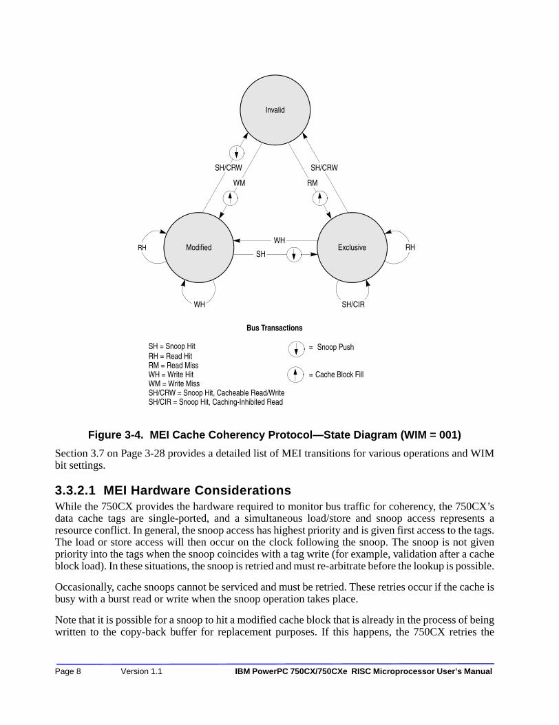
Figure 3-4. MEI Cache Coherency Protocol—State Diagram (WIM = 001)
Section 3.7 on Page 3-28 provides a detailed list of MEI transitions for various operations and WIMbit settings.
3.3.2.1 MEI Hardware ConsiderationsWhile the 750CX provides the hardware required to monitor bus traffic for coherency, the 750CX’sdata cache tags are single-ported, and a simultaneous load/store and snoop access represents aresource conflict. In general, the snoop access has highest priority and is given first access to the tags.The load or store access will then occur on the clock following the snoop. The snoop is not givenpriority into the tags when the snoop coincides with a tag write (for example, validation after a cacheblock load). In these situations, the snoop is retried and must re-arbitrate before the lookup is possible.
Occasionally, cache snoops cannot be serviced and must be retried. These retries occur if the cache isbusy with a burst read or write when the snoop operation takes place.
Note that it is possible for a snoop to hit a modified cache block that is already in the process of beingwritten to the copy-back buffer for replacement purposes. If this happens, the 750CX retries the
Bus Transactions
SH = Snoop Hit = Snoop PushRH = Read HitRM = Read MissWH = Write Hit = Cache Block FillWM = Write MissSH/CRW = Snoop Hit, Cacheable Read/WriteSH/CIR = Snoop Hit, Caching-Inhibited Read
SH/CRW
WM RM
SH/CRW
Invalid
ExclusiveModifiedRH RH
SH/CIRWH
WH
SH
Page 8 Versio
n 1.1 IBM PowerPC 750CX/750CXe RISC Microprocessor User’s Manual
snoop, and raises the priority of the castout operation to allow it to go to the bus before the cache blockfill.
Another consideration is page table aliasing. If a store hits to a modified cache block but the pagetable entry is marked write-through (WIMG = 1xxx), then the page has probably been aliased throughanother page table entry which is marked write-back (WIMG = 0xxx). If this occurs, the 750CXignores the modified bit in the cache tag. The cache block is updated during the write-throughoperation and the block remains in the modified state.
The global (GBL) signal, asserted as part of the address attribute field during a bus transaction,enables the snooping hardware of the 750CX. Address bus masters assert GBL to indicate that thecurrent transaction is a global access (that is, an access to memory shared by more than one device).If GBL is not asserted for the transaction, that transaction is not snooped by the 750CX. Note that theGBL signal is not asserted for instruction fetches, and that GBL is asserted for all data read or writeoperations when using real addressing mode (that is, address translation is disabled).
Normally, GBL reflects the M-bit value specified for the memory reference in the correspondingtranslation descriptor(s). Care should be taken to minimize the number of pages marked as global,because the retry protocol enforces coherency and can use considerable bus bandwidth if much datais shared. Therefore, available bus bandwidth decreases as more memory is marked as global.
The 750CX snoops a transaction if the transfer start (TS) and GBL signals are asserted together in thesame bus clock (this is a qualified snooping condition). No snoop update to the 750CX cache occursif the snooped transaction is not marked global. Also, because cache block castouts and snoop pushesdo not require snooping, the GBL signal is not asserted for these operations.
When the 750CX detects a qualified snoop condition, the address associated with the TS signal iscompared with the cache tags. Snooping finishes if no hit is detected. If, however, the address hits inthe cache, the 750CX reacts according to the MEI protocol shown in Figure 3-4 on Page 3-8.
3.3.3 Coherency Precautions in Single Processor SystemsThe following coherency paradoxes can be encountered within a single-processor system.
• Load or store to a caching-inhibited page (WIMG = x1xx) and a cache hit occurs.
The 750CX ignores any hits to a cache block in a memory space marked caching-inhibited (WIMG = x1xx). The access is performed on the external bus as if there were no hit. The data in the cache is not pushed, and the cache block is not invalidated.
• Store to a page marked write-through (WIMG = 1xxx) and a cache hit occurs to a modified cache block.
The 750CX ignores the modified bit in the cache tag. The cache block is updated during the write-through operation but the block remains in the modified state (M).
Note that when WIM bits are changed in the page tables or BAT registers, it is critical that the cachecontents reflect the new WIM bit settings. For example, if a block or page that had allowed cachingbecomes caching-inhibited, software should ensure that the appropriate cache blocks are flushed tomemory and invalidated.
Table of Contents 5/9/02 Page 9

3.3.4 Coherency Precautions in Multiprocessor SystemsThe 750CX’s three-state coherency protocol permits no data sharing between the 750CX and othercaches. All burst reads initiated by the 750CX are performed as read with intent to modify. Burstsnoops are interpreted as read with intent to modify or read with no intent to cache. This effectivelyplaces all caches in the system into a three-state coherency scheme. Four-state caches may share dataamongst themselves but not with the 750CX.
3.3.5 PowerPC 750CX-Initiated Load/Store Operations Load and store operations are assumed to be weakly ordered on the 750CX. The load/store unit (LSU)can perform load operations that occur later in the program ahead of store operations, even when thedata cache is disabled (see 3.3.5.2). However, strongly ordered load and store operations can beenforced through the setting of the I bit (of the page WIMG bits) when address translation is enabled.Note that when address translation is disabled (real addressing mode), the default WIMG bits causethe I bit to be cleared (accesses are assumed to be cacheable), and thus the accesses are weaklyordered. Refer to Section 5.2 on Page 5-18 for a description of the WIMG bits when addresstranslation is disabled.
The 750CX does not provide support for direct-store segments. Operations attempting to access adirect-store segment will invoke a DSI exception. For additional information about DSI exceptions,refer to Section 4.5.3 on Page 4-18.
3.3.5.1 Performed Loads and StoresThe PowerPC architecture defines a performed load operation as one that has the addressed memorylocation bound to the target register of the load instruction. The architecture defines a performed storeoperation as one where the stored value is the value that any other processor will receive whenexecuting a load operation (that is of course, until it is changed again). With respect to the 750CX,caching-allowed (WIMG = x0xx) loads and caching-allowed, write-back (WIMG = 00xx) stores areperformed when they have arbitrated to address the cache block. Note that in the event of a cachemiss, these storage operations may place a memory request into the processor’s memory queue, butsuch operations are considered an extension to the state of the cache with respect to snooping busoperations. Caching-inhibited (WIMG = x1xx) loads, caching-inhibited (WIMG = x1xx) stores, andwrite-through (WIMG = 1xxx) stores are performed when they have been successfully presented tothe external 60x bus.
3.3.5.2 Sequential Consistency of Memory AccessesThe PowerPC architecture requires that all memory operations executed by a single processor besequentially consistent with respect to that processor. This means that all memory accesses appear tobe executed in program order with respect to exceptions and data dependencies.
The 750CX achieves sequential consistency by operating a single pipeline to the cache/MMU. Allmemory accesses are presented to the MMU in exact program order and therefore exceptions aredetermined in order. Loads are allowed to bypass stores once exception checking has been performedfor the store, but data dependency checking is handled in the load/store unit so that a load will notbypass a store with an address match. Note that although memory accesses that miss in the cache areforwarded to the memory queue for future arbitration for the external bus, all potential synchronousexceptions have been resolved before the cache. In addition, although subsequent memory accessescan address the cache, full coherency checking between the cache and the memory queue is providedto avoid dependency conflicts.
Page 10 Version 1.1 IBM PowerPC 750CX/750CXe RISC Microprocessor User’s Manual

3.3.5.3 Atomic Memory ReferencesThe PowerPC architecture defines the Load Word and Reserve Indexed (lwarx) and the Store WordConditional Indexed (stwcx.) instructions to provide an atomic update function for a single, alignedword of memory. These instructions can be used to develop a rich set of multiprocessorsynchronization primitives.
NOTE: Atomic memory references constructed using lwarx/stwcx. instructions depend on the presence of a coherent memory system for correct operation. These instructions should not be expected to provide atomic access to noncoherent memory. For detailed information on these instructions, refer to Chapter 2, "Programming Model" and Chapter 12, "Instruction Set" in this book.
The lwarx instruction performs a load word from memory operation and creates a reservation for the32-byte section of memory that contains the accessed word. The reservation granularity is 32 bytes.The lwarx instruction makes a nonspecific reservation with respect to the executing processor and aspecific reservation with respect to other masters. This means that any subsequent stwcx. executed bythe same processor, regardless of address, will cancel the reservation. Also, any bus write or invalidateoperation from another processor to an address that matches the reservation address will cancel thereservation.
The stwcx. instruction does not check the reservation for a matching address. The stwcx. instructionis only required to determine whether a reservation exists. The stwcx. instruction performs a storeword operation only if the reservation exists. If the reservation has been cancelled for any reason, thenthe stwcx. instruction fails and clears the CR0[EQ] bit in the condition register. The architecturalintent is to follow the lwarx/stwcx. instruction pair with a conditional branch which checks to seewhether the stwcx. instruction failed.
If the page table entry is marked caching-allowed (WIMG = x0xx), and an lwarx access misses in thecache, then the 750CX performs a cache block fill. If the page is marked caching-inhibited (WIMG= x1xx) or the cache is locked, and the access misses, then the lwarx instruction appears on the busas a single-beat load. All bus operations that are a direct result of either an lwarx instruction or anstwcx. instruction are placed on the bus with a special encoding. Note that this does not force alllwarx instructions to generate bus transactions, but rather provides a means for identifying when anlwarx instruction does generate a bus transaction. If an implementation requires that all lwarxinstructions generate bus transactions, then the associated pages should be marked ascaching-inhibited.
The 750CX’s data cache treats all stwcx. operations as write-through independent of the WIMGsettings. However, if the stwcx. operation hits in the 750CX’s L2 cache, then the operation completeswith the reservation intact in the L2 cache. See Chapter 9, "L2 Cache" for more information.Otherwise, the stwcx. operation continues to the bus interface unit for completion. When thewrite-through operation completes successfully, either in the L2 cache or on the 60x bus, then the datacache entry is updated (assuming it hits), and CR0[EQ] is modified to reflect the success of theoperation. If the reservation is not intact, the stwcx. completes in the bus interface unit withoutperforming a bus transaction, and without modifying either of the caches.
Table of Contents 5/9/02 Page 11

3.4 Cache ControlThe 750CX’s L1 caches are controlled by programming specific bits in the HID0 special-purposeregister and by issuing dedicated cache control instructions. Section 3.4.1 describes the HID0 cachecontrol bits, and Section 3.4.2 on Page 3-14 describes the cache control instructions.
3.4.1 Cache Control Parameters in HID0The HID0 special-purpose register contains several bits that invalidate, disable, and lock theinstruction and data caches. The following sections describe these facilities.
3.4.1.1 Data Cache Flash InvalidationThe data cache is automatically invalidated when the 750CX is powered up and during a hard reset.However, a soft reset does not automatically invalidate the data cache. Software must use the HID0data cache flash invalidate bit (HID0[DCFI]) if data cache invalidation is desired after a soft reset.Once HID0[DCFI] is set through an mtspr operation, the 750CX automatically clears this bit in thenext clock cycle (provided that the data cache is enabled in the HID0 register).
Note that some PowerPC microprocessors accomplish data cache flash invalidation by setting andclearing HID0[DCFI] with two consecutive mtspr instructions (that is, the bit is not automaticallycleared by the microprocessor). Software that has this sequence of operations does not need to bechanged to run on the 750CX.
3.4.1.2 Data Cache Enabling/DisablingThe data cache may be enabled or disabled by using the data cache enable bit, HID0[DCE].HID0[DCE] is cleared on power-up, disabling the data cache.
When the data cache is in the disabled state (HID0[DCE] = 0), the cache tag state bits are ignored,and all accesses are propagated to the L2 cache or 60x bus as single-beat transactions. Note that theCI (cache inhibit) signal always reflects the state of the caching-inhibited memory/cache accessattribute (the I bit) independent of the state of HID0[DCE]. Also note that disabling the data cachedoes not affect the translation logic; translation for data accesses is controlled by MSR[DR].
The setting of the DCE bit must be preceded by a sync instruction to prevent the cache from beingenabled or disabled in the middle of a data access. In addition, the cache must be globally flushedbefore it is disabled to prevent coherency problems when it is re-enabled.
Snooping is not performed when the data cache is disabled.
The dcbz instruction will cause an alignment exception when the data cache is disabled. The touchload (dcbt and dcbtst) instructions are no-ops when the data cache is disabled. Other cacheoperations (caused by the dcbf, dcbst, and dcbi instructions) are not affected by disabling the cache.This can potentially cause coherency errors. For example, a dcbf instruction that hits a modified cacheblock in the disabled cache will cause a copyback to memory of potentially stale data.
3.4.1.3 Data Cache LockingThe contents of the data cache can be locked by setting the data cache lock bit, HID0[DLOCK]. Adata access that hits in a locked data cache is serviced by the cache. However, all accesses that missin the locked cache are propagated to the L2 cache or 60x bus as single-beat transactions. Note that
Page 12 Version 1.1 IBM PowerPC 750CX/750CXe RISC Microprocessor User’s Manual

the CI signal always reflects the state of the caching-inhibited memory/cache access attribute (the Ibit) independent of the state of HID0[DLOCK].
The 750CX treats snoop hits to a locked data cache the same as snoop hits to an unlocked data cache.However, any cache block invalidated by a snoop hit remains invalid until the cache is unlocked.
The setting of the DLOCK bit must be preceded by a sync instruction to prevent the data cache frombeing locked during a data access.
3.4.1.4 Instruction Cache Flash InvalidationThe instruction cache is automatically invalidated when the 750CX is powered up and during a hardreset. However, a soft reset does not automatically invalidate the instruction cache. Software must usethe HID0 instruction cache flash invalidate bit (HID0[ICFI]) if instruction cache invalidation isdesired after a soft reset. Once HID0[ICFI] is set through an mtspr operation, the 750CXautomatically clears this bit in the next clock cycle (provided that the instruction cache is enabled inthe HID0 register).
NOTE: Some PowerPC microprocessors accomplish instruction cache flash invalidation by setting and clearing HID0[ICFI] with two consecutive mtspr instructions (that is, the bit is not automatically cleared by the microprocessor). Software that has this sequence of operations does not need to be changed to run on the 750CX.
3.4.1.5 Instruction Cache Enabling/DisablingThe instruction cache may be enabled or disabled through the use of the instruction cache enable bit,HID0[ICE]. HID0[ICE] is cleared on power-up, disabling the instruction cache.
When the instruction cache is in the disabled state (HID[ICE] = 0), the cache tag state bits are ignored,and all instruction fetches are propagated to the L2 cache or 60x bus as single-beat transactions. Notethat the CI signal always reflects the state of the caching-inhibited memory/cache access attribute (theI bit) independent of the state of HID0[ICE]. Also note that disabling the instruction cache does notaffect the translation logic; translation for instruction accesses is controlled by MSR[IR].
The setting of the ICE bit must be preceded by an isync instruction to prevent the cache from beingenabled or disabled in the middle of an instruction fetch. In addition, the cache must be globallyflushed before it is disabled to prevent coherency problems when it is re-enabled. The icbi instructionis not affected by disabling the instruction cache.
3.4.1.6 Instruction Cache LockingThe contents of the instruction cache can be locked by setting the instruction cache lock bit,HID0[ILOCK]. An instruction fetch that hits in a locked instruction cache is serviced by the cache.However, all accesses that miss in the locked cache are propagated to the L2 cache or 60x bus assingle-beat transactions. Note that the CI signal always reflects the state of the caching-inhibitedmemory/cache access attribute (the I bit) independent of the state of HID0[ILOCK].
The setting of the ILOCK bit must be preceded by an isync instruction to prevent the instruction cachefrom being locked during an instruction fetch.
Table of Contents 5/9/02 Page 13

3.4.2 Cache Control InstructionsThe PowerPC architecture defines instructions for controlling both the instruction and data caches(when they exist). The cache control instructions, dcbt, dcbtst, dcbz, dcbst, dcbf, dcbi, and icbi, areintended for the management of the local L1 and L2 caches. The 750CX interprets the cache controlinstructions as if they pertain only to its own L1 or L2 caches. These instructions are not intended formanaging other caches in the system (except to the extent necessary to maintain coherency).
The 750CX does not snoop cache control instruction broadcasts, except for dcbz when M = 1. Thedcbz instruction is the only cache control instruction that causes a broadcast on the 60x bus (when M= 1) to maintain coherency. All other data cache control instructions (dcbi, dcbf, dcbst and dcbz) arenot broadcast, unless broadcast is enabled through the HID0[ABE] configuration bit. Note that dcbi,dcbf, dcbst and dcbz do broadcast to the 750CX’s L2 cache, regardless of HID0[ABE]. The icbiinstruction is never broadcast.
3.4.2.1 Data Cache Block Touch (dcbt) and Data Cache Block Touch for Store (dcbtst)
The Data Cache Block Touch (dcbt) and Data Cache Block Touch for Store (dcbtst) instructionsprovide potential system performance improvement through the use of software-initiated prefetchhints. The 750CX treats these instructions identically (that is, a dcbtst instruction behaves exactly thesame as a dcbt instruction on the 750CX). Note that PowerPC implementations are not required totake any action based on the execution of these instructions, but they may choose to prefetch the cacheblock corresponding to the effective address into their cache.
The 750CX loads the data into the cache when the address hits in the TLB or the BAT, is permittedload access from the addressed page, is not directed to a direct-store segment, and is directed at acacheable page. Otherwise, the 750CX treats these instructions as no-ops. The data brought into thecache as a result of this instruction is validated in the same manner that a load instruction would be(that is, it is marked as exclusive). The memory reference of a dcbt (or dcbtst) instruction causes thereference bit to be set. Note also that the successful execution of the dcbt (or dcbtst) instructionaffects the state of the TLB and cache LRU bits as defined by the PLRU algorithm.
3.4.2.2 Data Cache Block Zero (dcbz) The effective address is computed, translated, and checked for protection violations as defined in thePowerPC architecture. The dcbz instruction is treated as a store to the addressed byte with respect toaddress translation and protection.
If the block containing the byte addressed by the EA is in the data cache, all bytes are cleared, and thetag is marked as modified (M). If the block containing the byte addressed by the EA is not in the datacache and the corresponding page is caching-allowed, the block is established in the data cachewithout fetching the block from main memory, and all bytes of the block are cleared, and the tag ismarked as modified (M).
If the contents of the cache block are from a page marked memory coherence required (M = 1), anaddress-only bus transaction is run prior to clearing the cache block. The dcbz instruction is the onlycache control instruction that causes a broadcast on the 60x bus (when M = 1) to maintain coherency.The other cache control instructions are not broadcast unless broadcasting is specifically enabledthrough the HID0[ABE] configuration bit. The dcbz instruction executes regardless of whether thecache is locked, but if the cache is disabled, an alignment exception is generated. If the page
Page 14 Version 1.1 IBM PowerPC 750CX/750CXe RISC Microprocessor User’s Manual

containing the byte addressed by the EA is caching-inhibited or write-through, then the systemalignment exception handler is invoked. BAT and TLB protection violations generate DSI exceptions.
Note: If the target address of a dcbz instruction hits in the L1 cache, the 750CX requires four internalclock cycles to rewrite the cache block to zeros. On the first clock, the block is remarked asvalid-unmodified, and on the last clock the block is marked as valid-modified. If a snoop request tothat address is received during the middle two clocks of the dcbz operation, the 750CX does notproperly react to the snoop operation or generate an address retry (by an ARTRY assertion) to theother master. The other bus master continues reading the data from system memory, and both the750CX and the other bus master end up with different copies of the data. In addition, if the other busmaster has a cache, the cache block is marked valid in both caches, which is not allowed in the750CX’s three-state cache environment.
For this reason, avoid using dcbz for data that is shared in real time and that is not protected duringwriting through higher-level software synchronization protocols (such as semaphores). Use of dcbzmust be avoided for managing semaphores themselves. An alternative solution could be to preventdcbz from hitting in the L1 cache by performing a dcbf to that address beforehand.
3.4.2.3 Data Cache Block Store (dcbst)The effective address is computed, translated, and checked for protection violations as defined in thePowerPC architecture. This instruction is treated as a load with respect to address translation andmemory protection.
If the address hits in the cache and the cache block is in the exclusive (E) state, no action is taken. Ifthe address hits in the cache and the cache block is in the modified (M) state, the modified block iswritten back to memory and the cache block is placed in the exclusive (E) state.
The execution of a dcbst instruction does not broadcast on the 60x bus unless broadcast is enabledthrough the HID0[ABE] bit. The function of this instruction is independent of the WIMG bit settingsof the block containing the effective address. The dcbst instruction executes regardless of whether thecache is disabled or locked; however, a BAT or TLB protection violation generates a DSI exception.
3.4.2.4 Data Cache Block Flush (dcbf)The effective address is computed, translated, and checked for protection violations as defined in thePowerPC architecture. This instruction is treated as a load with respect to address translation andmemory protection.
If the address hits in the cache, and the block is in the modified (M) state, the modified block is writtenback to memory and the cache block is placed in the invalid (I) state. If the address hits in the cache,and the cache block is in the exclusive (E) state, the cache block is placed in the invalid (I) state. Ifthe address misses in the cache, no action is taken.
The execution of dcbf does not broadcast on the 60x bus unless broadcast is enabled through theHID0[ABE] bit. The function of this instruction is independent of the WIMG bit settings of the blockcontaining the effective address. The dcbf instruction executes regardless of whether the cache isdisabled or locked; however, a BAT or TLB protection violation generates a DSI exception.
Table of Contents 5/9/02 Page 15

3.4.2.5 Data Cache Block Invalidate (dcbi)The effective address is computed, translated, and checked for protection violations as defined in thePowerPC architecture. This instruction is treated as a store with respect to address translation andmemory protection.
If the address hits in the cache, the cache block is placed in the invalid (I) state, regardless of whetherthe data is modified. Because this instruction may effectively destroy modified data, it is privileged(that is, dcbi is available to programs at the supervisor privilege level, MSR[PR] = 0). The executionof dcbi does not broadcast on the 60x bus unless broadcast is enabled through the HID0[ABE] bit.The function of this instruction is independent of the WIMG bit settings of the block containing theeffective address. The dcbi instruction executes regardless of whether the cache is disabled or locked;however, a BAT or TLB protection violation generates a DSI exception.
3.4.2.6 Instruction Cache Block Invalidate (icbi)For the icbi instruction, the effective address is not computed or translated, so it cannot generate aprotection violation or exception. This instruction performs a virtual lookup into the instruction cache(index only). All ways of the selected instruction cache set are invalidated.
The icbi instruction is not broadcast on the 60x bus. The icbi instruction invalidates the cache blocksindependent of whether the cache is disabled or locked.
3.5 Cache OperationsThis section describes the 750CX’s cache operations.
3.5.1 Cache Block Replacement/Castout OperationsBoth the instruction and data cache use a pseudo least-recently-used (PLRU) replacement algorithmwhen a new block needs to be placed in the cache. When the data to be replaced is in the modified(M) state, that data is written into a castout buffer while the missed data is being accessed on the bus.When the load completes, the 750CX then pushes the replaced cache block from the castout buffer tothe L2 cache (if L2 is enabled) or to main memory (if L2 is disabled).
The replacement logic first checks to see if there are any invalid blocks in the set and chooses thelowest-order, invalid block (L[0–7]) as the replacement target. If all eight blocks in the set are valid,the PLRU algorithm is used to determine which block should be replaced. The PLRU algorithm isshown in Figure 3-5 on Page 3-17.
Each cache is organized as eight blocks per set by 128 sets. There is a valid bit for each block in thecache, L[0–7]. When all eight blocks in the set are valid, the PLRU algorithm is used to select thereplacement target. There are seven PLRU bits, B[0–6] for each set in the cache. For every hit in thecache, the PLRU bits are updated using the rules specified in Table 3-2 on Page 3-18.
Page 16 Version 1.1 IBM PowerPC 750CX/750CXe RISC Microprocessor User’s Manual

Figure 3-5. PLRU Replacement Algorithm
ReplaceL0
ReplaceL1
ReplaceL2
ReplaceL3
ReplaceL4
ReplaceL5
ReplaceL6
ReplaceL7
B0 = 0
B4 = 0
B1 = 0 B1 = 1 B2 = 1B2 = 0
B0 = 1
B3 = 0 B3 = 1 B4 = 1 B5 = 0 B5 = 1 B6 = 0 B6 = 1
AllocateL0L0 invalid
AllocateL2L2 invalid
AllocateL1L1 invalid
AllocateL3L3 invalid
AllocateL4L4 invalid
AllocateL5L5 invalid
AllocateL6L6 invalid
AllocateL7L7 invalid
L7 valid
L0 valid
L1 valid
L2 valid
L3 valid
L4 valid
L5 valid
L6 valid
Table of Contents 5/9/02 Page 17

If all eight blocks are valid, then a block is selected for replacement according to the PLRU bitencodings shown in Table 3-3.
During power-up or hard reset, all the valid bits of the blocks are cleared and the PLRU bits clearedto point to block L0 of each set. Note that this is also the state of the data or instruction cache aftersetting their respective flash invalidate bit (HID0[DCFI] or HID0[ICFI]).
Table 3-2. PLRU Bit Update Rules
If the Current
Access is To:
Then the PLRU bits are Changed to:1
B0 B1 B2 B3 B4 B5 B6
L0 1 1 x 1 x x x
L1 1 1 x 0 x x x
L2 1 0 x x 1 x x
L3 1 0 x x 0 x x
L4 0 x 1 x x 1 x
L5 0 x 1 x x 0 x
L6 0 x 0 x x x 1
L7 0 x 0 x x x 0
Note: 1x = Does not change
Table 3-3. PLRU Replacement Block Selection
If the PLRU Bits Are:
Then the Block
Selected for Replacement
Is:
B0
0
B1
0B3
0 L0
0 0 1 L1
0 1B4
0 L2
0 1 1 L3
1
B2
0B5
0 L4
1 0 1 L5
1 1B6
0 L6
1 1 1 L7
Page 18 Version 1.1 IBM PowerPC 750CX/750CXe RISC Microprocessor User’s Manual

3.5.2 Cache Flush OperationsThe instruction cache can be invalidated by executing a series of icbi instructions or by settingHID0[ICFI]. The data cache can be invalidated by executing a series of dcbi instructions or by settingHID0[DCFI].
Any modified entries in the data cache can be copied back to memory (flushed) by using the dcbfinstruction or by executing a series of 12 uniquely addressed load or dcbz instructions to each of the128 sets. The address space should not be shared with any other process to prevent snoop hitinvalidations during the flushing routine. Exceptions should be disabled during this time so that thePLRU algorithm does not get disturbed.
The data cache flush assist bit, HID0[DCFA], simplifies the software flushing process. When set,HID0[DCFA] forces the PLRU replacement algorithm to ignore the invalid entries and follow thereplacement sequence defined by the PLRU bits. This reduces the series of uniquely addressed loador dcbz instructions to eight per set. HID0[DCFA] should be set just prior to the beginning of thecache flush routine and cleared after the series of instructions is complete.
3.5.3 Data Cache-Block-Fill OperationsThe 750CX’s data cache blocks are filled in four beats of 64 bits each, with the critical double wordloaded first. The data cache is not blocked to internal accesses while the load (caused by a cache miss)completes. This functionality is sometimes referred to as ‘hits under misses,’ because the cache canservice a hit while a cache miss fill is waiting to complete. The critical-double-word read frommemory is simultaneously written to the data cache and forwarded to the requesting unit, thusminimizing stalls due to cache fill latency.
A cache block is filled after a read miss or write miss (read-with-intent-to-modify) occurs in thecache. The cache block that corresponds to the missed address is updated by a burst transfer of thedata from the L2 or system memory. Note that if a read miss occurs in a system with multiple busmasters, and the data is modified in another cache, the modified data is first written to externalmemory before the cache fill occurs.
3.5.4 Instruction Cache-Block-Fill OperationsThe 750CX’s instruction cache blocks are loaded in four beats of 64 bits each, with the critical doubleword loaded first. The instruction cache is not blocked to internal accesses while the fetch (caused bya cache miss) completes. On a cache miss, the critical and following double words read from memoryare simultaneously written to the instruction cache and forwarded to the instruction queue, thusminimizing stalls due to cache fill latency. There is no snooping of the instruction cache.
3.5.5 Data Cache-Block-Push OperationWhen a cache block in the 750CX is snooped and hit by another bus master and the data is modified,the cache block must be written to memory and made available to the snooping device. The cacheblock is said to be pushed out onto the 60x bus.
3.6 L1 Caches and 60x Bus TransactionsThe 750CX transfers data to and from the cache in single-beat transactions of two words, or infour-beat transactions of eight words which fill a cache block. Single-beat bus transactions can
Table of Contents 5/9/02 Page 19

transfer from one to eight bytes to or from the 750CX, and can be misaligned. Single-beat transactionscan be caused by cache write-through accesses, caching-inhibited accesses (WIMG = x1xx), accesseswhen the cache is disabled (HID0[DCE] bit is cleared), or accesses when the cache is locked(HID0[DLOCK] bit is cleared).
Burst transactions on the 750CX always transfer eight words of data at a time, and are aligned to adouble-word boundary. The 750CX transfer burst (TBST) output signal indicates to the systemwhether the current transaction is a single-beat transaction or four-beat burst transfer. Bursttransactions have an assumed address order. For cacheable read operations, instruction fetches, orcacheable, non-write-through write operations that miss the cache, the 750CX presents thedouble-word-aligned address associated with the load/store instruction or instruction fetch thatinitiated the transaction.
As shown in Figure 3-6, the first quad word contains the address of the load/store or instruction fetchthat missed the cache. This minimizes latency by allowing the critical code or data to be forwardedto the processor before the rest of the block is filled. For all other burst operations, however, the entireblock is transferred in order (oct-word-aligned). Critical-double-word-first fetching on a cache missapplies to both the data and instruction cache.
Figure 3-6. 750CX Cache Addresses
3.6.1 Read Operations and the MEI ProtocolThe MEI coherency protocol affects how the 750CX data cache performs read operations on the 60xbus. All reads (except for caching-inhibited reads) are encoded on the bus asread-with-intent-to-modify (RWITM) to force flushing of the addressed cache block from othercaches in the system.
The MEI coherency protocol also affects how the 750CX snoops read operations on the 60x bus. Allreads snooped from the 60x bus (except for caching-inhibited reads) are interpreted as RWITM tocause flushing from the 750CX’s cache. Single-beat reads (TBST negated) are interpreted by the750CX as caching inhibited.
If the address requested is in double-word A, the address placed on the bus is that of double-word A, andthe four data beats are ordered in the following manner:
If the address requested is in double-word C, the address placed on the bus will be that of double-word C,and the four data beats are ordered in the following manner:
A B C D
111000 01
A B C D
320 1Beat
Bits (27... 28)
C D A B
320 1Beat
750CX Cache Address
Page
20 Version 1.1 IBM PowerPC 750CX/750CXe RISC Microprocessor User’s Manual
These actions for read operations allow the 750CX to operate successfully (coherently) on the buswith other bus masters that implement either the three-state MEI or a four-state MESI cachecoherency protocol.
3.6.2 Bus Operations Caused by Cache Control InstructionsThe cache control, TLB management, and synchronization instructions supported by the 750CX mayaffect or be affected by the operation of the 60x bus. The operation of the instructions may alsoindirectly cause bus transactions to be performed, or their completion may be linked to the bus.
The dcbz instruction is the only cache control instruction that causes an address-only broadcast onthe 60x bus. All other data cache control instructions (dcbi, dcbf, dcbst, and dcbz) are not broadcastunless specifically enabled through the HID0[ABE] configuration bit. Note that dcbi, dcbf, dcbst,and dcbz do broadcast to the 750CX’s L2 cache, regardless of HID0[ABE]. HID0[ABE] also controlsthe broadcast of the sync and eieio instructions.
The icbi instruction is never broadcast. No broadcasts by other masters are snooped by the 750CX(except for dcbz kill block transactions). For detailed information on the cache control instructions,refer to Chapter 2, "Programming Model" and Chapter 12, "Instruction Set" in this book.
Table 3-4 provides an overview of the bus operations initiated by cache control instructions. Note thatthe information in this table assumes that the WIM bits are set to 001; that is, the cache is operatingin write-back mode, caching is permitted and coherency is enforced.
Table 3-4. Bus Operations Caused by Cache Control Instructions (WIM = 001)
InstructionCurrent
Cache StateNext Cache State Bus Operation Comment
sync Don’t care No change sync (if enabled in HID0[ABE])
Waits for memory queues to complete bus activity
tlbie — — None —
tlbsync — — None Waits for the negation of the TLBSYNC input signal to complete
eieio Don’t care No change eieio (if enabled in HID0[ABE])
Address-only bus operation
icbi Don’t care I None —
dcbi Don’t care I Kill block (if enabled in HID0[ABE])
Address-only bus operation
dcbf I, E I Flush block(if enabled in HID0[ABE])
Address-only bus operation
dcbf M I Write with kill Block is pushed
dcbst I, E No change Clean block(if enabled in HID0[ABE])
Address-only bus operation
dcbst M E Write with kill Block is pushed
dcbz I M Write with kill —
Table of Contents 5/9/02 Page 21

For additional details about the specific bus operations performed by the 750CX, see Chapter 8, "BusInterface Operation" in this manual.
3.6.3 SnoopingThe 750CX maintains data cache coherency in hardware by coordinating activity between the datacache, the bus interface logic, the L2 cache, and the memory system. The 750CX has a copy-backcache which relies on bus snooping to maintain cache coherency with other caches in the system. Forthe 750CX, the coherency size of the bus is the size of a cache block, 32 bytes. This means that anybus transactions that cross an aligned 32-byte boundary must present a new address onto the bus atthat boundary for proper snoop operation by the 750CX, or they must operate noncoherently withrespect to the 750CX.
As bus operations are performed on the bus by other bus masters, the 750CX’s bus snooping logicmonitors the addresses and transfer attributes that are referenced. The 750CX snoops the bustransactions during the cycle that TS is asserted for any of the following qualified snoop conditions:
• The global signal (GBL) is asserted indicating that coherency enforcement is required.
• A reservation is currently active in the 750CX as the result of an lwarx instruction, and the transfer type attributes (TT[0–4]) indicate a write or kill operation. These transactions are snooped regardless of whether GBL is asserted to support reservations in the MEI cache protocol.
All transactions snooped by the 750CX are checked for correct address bus parity. Every assertion ofTS detected by the 750CX (whether snooped or not) must be followed by an accompanying assertionof AACK.
Once a qualified snoop condition is detected on the bus, the snooped address associated with TS iscompared against the data cache tags, memory queues, and/or other storage elements as appropriate.The L1 data cache tags and L2 cache tags are snooped for standard data cache coherency support. Nosnooping is done in the instruction cache for coherency.
The memory queues are snooped for pipeline collisions and memory coherency collisions. A pipelinecollision is detected when another bus master addresses any portion of a line that this 750CX’s datacache is currently in the process of loading (L1 loading from L2, or L1/L2 loading from memory). Amemory coherency collision occurs when another bus master addresses any portion of a line that the750CX has currently queued to write to memory from the data cache (castout or copy-back), but hasnot yet been granted bus access to perform.
dcbz E, M M Kill block Writes over modified data
dcbt I E Read-with-intent-to-modify
Fetched cache block is stored in the cache
dcbt E, M No change None —
dcbtst I E Read-with-intent-to-modify
Fetched cache block is stored in the cache
dcbtst E,M No change None —
Table 3-4. Bus Operations Caused by Cache Control Instructions (WIM = 001)
InstructionCurrent
Cache StateNext Cache State Bus Operation Comment
Page 22 Version 1.1 IBM PowerPC 750CX/750CXe RISC Microprocessor User’s Manual

If a snooped transaction results in a cache hit or pipeline collision or memory queue collision, the750CX asserts ARTRY on the 60x bus. The current bus master, detecting the assertion of the ARTRYsignal, should abort the transaction and retry it at a later time, so that the 750CX can first perform awrite operation back to memory from its cache or memory queues. The 750CX may also retry a bustransaction if it is unable to snoop the transaction on that cycle due to internal resource conflicts.Additional snoop action may be forwarded to the cache as a result of a snoop hit in some cases (acache push of modified data, or a cache block invalidation). There is no immediate way for anotherCPU bus agent to determine the cause of the 750CX ARTRY.
Implementation Note: Snooping of the memory queues for pipeline collisions, as described above,is performed for burst read operations in progress only. In this case, the read address has completedon the bus, however, the data tenure may be either in-progress or not yet started by the processor.During this time the 750CX will retry any other global access to that line by another bus master untilall data has been received in it’s L1 cache. Pipeline collisions, however, do not apply for burst writeoperations in progress. If the 750CX has completed an address tenure for a burst write, and iscurrently waiting for a data bus grant or is currently transferring data to memory, it will not generatean address retry to another bus master that addresses the line. It is the responsibility of the memorysystem to handle this collision (usually by keeping the data transactions to memory in order). Notealso that all burst writes by the 750CX are performed as non-global, and hence do not normally enablesnooping, even for address collision purposes. (Snooping may still occur for reservation cancellingpurposes.)
3.6.4 Snoop Response to 60x Bus TransactionsThere are several bus transaction types defined for the 60x bus. The transactions in Table 3-5correspond to the transfer type signals TT[0–4], which are described in Section 7.2.4.1 on Page 7-6.
The 750CX never retries a transaction in which GBL is not asserted, even if the tags are busy or thereis a tag hit. Reservations are snooped regardless of the state of GBL.
Table 3-5. Response to Snooped Bus Transactions
Snooped Transaction TT[0–4] 750CX Response
Clean block 00000 No action is taken.
Flush block 00100 No action is taken.
SYNC 01000 No action is taken.
Kill block 01100 The kill block operation is an address-only bus transaction initiated when a dcbz or dcbi instruction is executed• If the addressed cache block is in the exclusive (E) state, the cache
block is placed in the invalid (I) state. • If the addressed cache block is in the modified (M) state, the 750CX
asserts ARTRY and initiates a push of the modified block out of the cache and the cache block is placed in the invalid (I) state.
• If the address misses in the cache, no action is taken. Any reservation associated with the address is canceled.
EIEIO 10000 No action is taken.
External control word write
10100 No action is taken.
Table of Contents 5/9/02 Page 23

TLB invalidate 11000 No action is taken.
External control word read
11100 No action is taken.
lwarx reservation set 00001 No action is taken.
Reserved 00101 —
TLBSYNC 01001 No action is taken.
ICBI 01101 No action is taken.
Reserved 1XX01 —
Write-with-flush 00010 A write-with-flush operation is a single-beat or burst transaction initiated when a caching-inhibited or write-through store instruction is executed. • If the addressed cache block is in the exclusive (E) state, the cache
block is placed in the invalid (I) state. • If the addressed cache block is in the modified (M) state, the 750CX
asserts ARTRY and initiates a push of the modified block out of the cache and the cache block is placed in the invalid (I) state.
• If the address misses in the cache, no action is taken. Any reservation associated with the address is canceled.
Write-with-kill 00110 A write-with-kill operation is a burst transaction initiated due to a castout, caching-allowed push, or snoop copy -back. • If the address hits in the cache, the cache block is placed in the
invalid (I) state (killing modified data that may have been in the block).
• If the address misses in the cache, no action is taken. Any reservation associated with the address is canceled.
Read 01010 A read operation is used by most single-beat and burst load transactions on the bus.For single-beat, caching-inhibited read transaction: • If the addressed cache block is in the exclusive (E) state, the cache
block remains in the exclusive (E) state. • If the addressed cache block is in the modified (M) state, the 750CX
asserts ARTRY and initiates a push of the modified block out of the cache and the cache block is placed in the exclusive (E) state.
• If the address misses in the cache, no action is taken. For burst read transactions: • If the addressed cache block is in the exclusive (E) state, the cache
block is placed in the invalid (I) state. • If the addressed cache block is in the modified (M) state, the 750CX
asserts ARTRY and initiates a push of the modified block out of the cache and the cache block is placed in the invalid (I) state.
• If the address misses in the cache, no action is taken.
Table 3-5. Response to Snooped Bus Transactions (Continued)
Snooped Transaction TT[0–4] 750CX Response
Page 24 Version 1.1 IBM PowerPC 750CX/750CXe RISC Microprocessor User’s Manual

Read-with-intent-to-modify (RWITM)
01110 A RWITM operation is issued to acquire exclusive use of a memory location for the purpose of modifying it. • If the addressed cache block is in the exclusive (E) state, the cache
block is placed in the invalid (I) state. • If the addressed cache block is in the modified (M) state, the 750CX
asserts ARTRY and initiates a push of the modified block out of the cache and the cache block is placed in the invalid (I) state.
• If the address misses in the cache, no action is taken.
Write-with-flush-atomic 10010 Write-with-flush-atomic operations occur after the processor issues an stwcx. instruction. • If the addressed cache block is in the exclusive (E) state, the cache
block is placed in the invalid (I) state. • If the addressed cache block is in the modified (M) state, the 750CX
asserts ARTRY and initiates a push of the modified block out of the cache and the cache block is placed in the invalid (I) state.
• If the address misses in the cache, no action is taken. Any reservation is canceled, regardless of the address.
Reserved 10110 —
Read-atomic 11010 Read atomic operations appear on the bus in response to lwarx instructions and generate the same snooping responses as read operations.
Read-with-intent-to-modify-atomic
11110 The RWITM atomic operations appear on the bus in response to stwcx. instructions and generate the same snooping responses as RWITM operations.
Reserved 00011 —
Reserved 00111 —
Read-with-no-intent-to-cache (RWNITC)
01011 A RWNITC operation is issued to acquire exclusive use of a memory location with no intention of modifying the location. • If the addressed cache block is in the exclusive (E) state, the cache
block remains in the exclusive (E) state. • If the addressed cache block is in the modified (M) state, the 750CX
asserts ARTRY and initiates a push of the modified block out of the cache and the cache block is placed in the exclusive (E) state.
• If the address misses in the cache, no action is taken.
Reserved 01111 —
Reserved 1XX11 —
Table 3-5. Response to Snooped Bus Transactions (Continued)
Snooped Transaction TT[0–4] 750CX Response
Table of Contents 5/9/02 Page 25

3.6.5 Transfer AttributesIn addition to the address and transfer type signals, the 750CX supports the transfer attribute signalsTBST, TSIZ[0–2], WT, CI, and GBL. The TBST and TSIZ[0–2] signals indicate the data transfer sizefor the bus transaction.
The WT signal reflects the write-through status (the complement of the W bit) for the transaction asdetermined by the MMU address translation during write operations. WT is asserted for burst writesdue to dcbf (flush) and dcbst (clean) instructions, and for snoop pushes; WT is negated for ecowxtransactions. Since the write-through status is not meaningful for reads, the 750CX uses the WTsignal during read transactions to indicate that the transaction is an instruction fetch (WT negated),or not an instruction fetch (WT asserted).
The CI signal reflects the caching-inhibited/allowed status (the complement of the I bit) of thetransaction as determined by the MMU address translation even if the L1 caches are disabled orlocked. CI is always asserted for eciwx/ecowx bus transactions independent of the address translation.
The GBL signal reflects the memory coherency requirements (the complement of the M bit) of thetransaction as determined by the MMU address translation. Castout and snoop copy-back operations(TT[0–4] = 00110) are generally marked as nonglobal (GBL negated) and are not snooped (exceptfor reservation monitoring). Other masters, however, may perform DMA write operations with thisencoding but marked global (GBL asserted) and thus must be snooped.
Table 3-6 summarizes the address and transfer attribute information presented on the bus by the750CX for various master or snoop-related transactions.
Page 26 Version 1.1 IBM PowerPC 750CX/750CXe RISC Microprocessor User’s Manual

Table 3-6. Address/Transfer Attribute Summary
Bus Transaction A[0–31] TT[0–4] TBST TSIZ[0–2] GBL WT CI
Instruction fetch operations:
Burst (caching-allowed) PA[0–28] || 0b000 0 1 1 1 0 0 0 1 0 ¬ M 1 1*
Single-beat read (caching-inhibited or cache disabled)
PA[0–28] || 0b000 0 1 0 1 0 1 0 0 0 ¬ M 1 ¬ I
Data cache operations:
Cache block fill (due to load or store miss)
PA[0–28] || 0b000 A 1 1 1 0 0 0 1 0 ¬ M 0 1*
Castout (normal replacement)
CA[0–26] || 0b00000 0 0 1 1 0 0 0 1 0 1 1 1*
Push (cache block push due to dcbf/dcbst)
PA[0–26] || 0b00000 0 0 1 1 0 0 0 1 0 1 0 1*
Snoop copyback CA[0–26] || 0b00000 0 0 1 1 0 0 0 1 0 1 0 1*Data cache bypass operations:
Single-beat read (caching-inhibited or cache disabled)
PA[0–31] A 1 0 1 0 1 S S S ¬ M 0 ¬ I
Single-beat write (caching-inhibited, write-through, or cache disabled)
PA[0–31] 0 0 0 1 0 1 S S S ¬ M ¬W ¬ I
Special instructions:
dcbz (addr-only) PA[0–28] || 0b000 0 1 1 0 0 0 0 1 0 0* 0 1*dcbi (if HID0[ABE] = 1, addr-only)
PA[0–26] || 0b00000 0 1 1 0 0 0 0 1 0 ¬ M 0 1*
dcbf (if HID0[ABE] = 1, addr-only)
PA[0–26] || 0b00000 0 0 1 0 0 0 0 1 0 ¬ M 0 1*
dcbst (if HID0[ABE] = 1, addr-only)
PA[0–26] || 0b00000 0 0 0 0 0 0 0 1 0 ¬ M 0 1*
sync (if HID0[ABE] = 1, addr-only)
0x0000_0000 0 1 0 0 0 0 0 1 0 0 0 0
eieio (if HID0[ABE] = 1, addr-only)
0x0000_0000 1 0 0 0 0 0 0 1 0 0 0 0
stwcx. (always single-beat write) PA[0–29] || 0b00 1 0 0 1 0 1 1 0 0 ¬ M ¬ W ¬ I
eciwx PA[0–29] || 0b00 1 1 1 0 0 EAR[28–31] 1 0 0
ecowx PA[0–29] || 0b00 1 0 1 0 0 EAR[28–31] 1 1 0Notes:PA = Physical address, CA = Cache address.W,I,M = WIM state from address translation; ¬ = complement; 0*or 1* = WIM state implied by transaction type in tableFor instruction fetches, reflection of the M bit must be enabled through HID0[IFEM].A = Atomic; high if lwarx, low otherwiseS = Transfer sizeSpecial instructions listed may not generate bus transactions depending on cache state.
Table of Contents 5/9/02 Page 27

3.7 MEI State TransactionsTable 3-7 shows MEI state transitions for various operations. Bus operations are described inTable 3-4 on Page 3-21.
Table 3-7. MEI State Transitions
OperationCache
Operation Bus sync
WIMCurrent Cache State
Next Cache State
Cache ActionsBus
Operation
Load(T = 0)
Read No x0x I Same 1 Cast out of modified block (as required)
Write-with-kill
2 Pass four-beat read to memory queue
Read
Load(T = 0)
Read No x0x E,M Same Read data from cache —
Load (T = 0) Read No x1x I Same Pass single-beat read to memory queue
Read
Load (T = 0) Read No x1x E I CRTRY read —
Load (T = 0) Read No x1x M I CRTRY read (push sector to write queue)
Write-with-kill
lwarx Read Acts like other reads but bus operation uses special encoding
Store(T = 0)
Write No 00x I Same Cast out of modified block (if necessary)
Write-with-kill
Pass RWITM to memory queue
RWITM
Store(T = 0)
Write No 00x E,M M Write data to cache —
Store ¦ stwcx.(T = 0)
Write No 10x I Same Pass single-beat write to memory queue
Write-with-flush
Store ¦ stwcx.(T = 0)
Write No 10x E Same Write data to cache —
Pass single-beat write to memory queue
Write-with-flush
Store ¦ stwcx.(T = 0)
Write No 10x M Same CRTRY write —
Push block to write queue
Write-with-kill
Store (T = 0)or stwcx. (WIM = 10x)
Write No x1x I Same Pass single-beat write to memory queue
Write-with-flush
Store (T = 0)or stwcx. (WIM = 10x)
Write No x1x E I CRTRY write —
Page 28 Version 1.1 IBM PowerPC 750CX/750CXe RISC Microprocessor User’s Manual

Store (T = 0)or stwcx. (WIM = 10x)
Write No x1x M I CRTRY write —
Push block to write queue
Write-with-kill
stwcx. Conditional write
If the reserved bit is set, this operation is like other writes except the bus operation uses a special encoding.
dcbf Data cache block flush
No xxx I,E Same CRTRY dcbf —
Pass flush Flush
Same I State change only —
dcbf Data cache block flush
No xxx M I Push block to write queue
Write-with-kill
dcbst Data cache block store
No xxx I,E Same CRTRY dcbst —
Pass clean Clean
Same Same No action —
dcbst Data cache block store
No xxx M E Push block to write queue
Write-with-kill
dcbz Data cache block set to zero
No x1x x x Alignment trap —
dcbz Data cache block set to zero
No 10x x x Alignment trap —
dcbz Data cache block set to zero
Yes 00x I Same CRTRY dcbz —
Cast out of modified block
Write-with-kill
Pass kill Kill
Same M Clear block —
dcbz Data cache block set to zero
No 00x E,M M Clear block —
dcbt Data cache block touch
No x1x I Same Pass single-beat read to memory queue
Read
dcbt Data cache block touch
No x1x E I CRTRY read —
dcbt Data cache block touch
No x1x M I CRTRY read —
Push block to write queue
Write-with-kill
Table 3-7. MEI State Transitions (Continued)
OperationCache
Operation Bus sync
WIMCurrent Cache State
Next Cache State
Cache ActionsBus
Operation
Table of Contents 5/9/02 Page 29

NOTE: Single-beat writes are not snooped in the write queue.
dcbt Data cache block touch
No x0x I Same Cast out of modified block (as required)
Write-with-kill
Pass four-beat read to memory queue
Read
dcbt Data cache block touch
No x0x E,M Same No action —
Single-beat read
Reload dump 1
No xxx I Same Forward data_in —
Four-beat read (double-word-aligned)
Reload dump
No xxx I E Write data_in to cache —
Four-beat write (double-word-aligned)
Reload dump
No xxx I M Write data_in to cache —
E→I Snoopwrite or kill
No xxx E I State change only (committed)
—
M→I Snoopkill
No xxx M I State change only (committed)
—
PushM→I
Snoopflush
No xxx M I Conditionally push Write-with-kill
PushM→E
Snoopclean
No xxx M E Conditionally push Write-with-kill
tlbie TLB invalidate
No xxx x x CRTRY TLBI —
Pass TLBI —
No action —
sync Synchroni-zation
No xxx x x CRTRY sync —
Pass sync —
No action —
Table 3-7. MEI State Transitions (Continued)
OperationCache
Operation Bus sync
WIMCurrent Cache State
Next Cache State
Cache ActionsBus
Operation
Page 30 Version 1.1 IBM PowerPC 750CX/750CXe RISC Microprocessor User’s Manual

Chapter 4 Exceptions4040
The OEA portion of the PowerPC architecture defines the mechanism by which PowerPC processorsimplement exceptions (referred to as interrupts in the architecture specification). Exceptionconditions may be defined at other levels of the architecture. For example, the UISA definesconditions that may cause floating-point exceptions; the OEA defines the mechanism by which theexception is taken.
The PowerPC exception mechanism allows the processor to change to supervisor state as a result ofunusual conditions arising in the execution of instructions and from external signals, bus errors, orvarious internal conditions. When exceptions occur, information about the state of the processor issaved to certain registers and the processor begins execution at an address (exception vector)predetermined for each exception. Processing of exceptions begins in supervisor mode.
Although multiple exception conditions can map to a single exception vector, often a more specificcondition may be determined by examining a register associated with the exception—for example,the DSISR and the floating-point status and control register (FPSCR). The high order bits of the MSRare also set for some exceptions. Also, software can explicitly enable or disable some exceptionconditions.
The PowerPC architecture requires that exceptions be taken in program order; therefore, although aparticular implementation may recognize exception conditions out of order, they are handled strictlyin order with respect to the instruction stream. When an instruction-caused exception is recognized,any unexecuted instructions that appear earlier in the instruction stream, including any that have notyet entered the execute state, are required to complete before the exception is taken. For example, ifa single instruction encounters multiple exception conditions, those exceptions are taken and handledbased on the priority of the exception. Likewise, exceptions that are asynchronous and precise arerecognized when they occur, but are not handled until all instructions currently in the execute stagesuccessfully complete execution and report their results.
To prevent loss of state information, exception handlers must save the information stored in themachine status save/restore registers, SRR0 and SRR1, soon after the exception is taken to preventthis information from being lost due to another exception being taken. Because exceptions can occurwhile an exception handler routine is executing, multiple exceptions can become nested. It is up tothe exception handler to save the necessary state information if control is to return to the exceptingprogram.
In many cases, after the exception handler returns, there is an attempt to execute the instruction thatcaused the exception (e.g., page fault). Instruction execution continues until the next exceptioncondition is encountered. Recognizing and handling exception conditions sequentially guaranteesthat the machine state is recoverable and processing can resume without losing instruction results.
In this book, the following terms are used to describe the stages of exception processing.
Recognition Exception recognition occurs when the condition that can cause an exception is identified by the processor.
Taken An exception is said to be taken when control of instruction execution is passed to the exception handler; that is, the context is saved and the instruction at the appropriate vector offset is fetched and the exception handler routine is begun in supervisor mode.
Table of Contents 5/9/02 Page 1

Handling Exception handling is performed by the software linked to the appropriate vector offset. Exception handling is begun in supervisor mode (referred to as privileged state in the architecture specification).
NOTE: The PowerPC architecture documentation refers to exceptions as interrupts. In this book, the term ‘interrupt’ is reserved to refer to asynchronous exceptions and sometimes to the event that causes the exception. Also, the PowerPC architecture uses the word ‘exception’ to refer to IEEE-defined floating-point exception conditions that may cause a program exception to be taken; see Section 4.5.7. The occurrence of these IEEE exceptions may not cause an exception to be taken. IEEE-defined exceptions are referred to as IEEE floating-point exceptions or floating-point exceptions.
4.1 PowerPC 750CX Microprocessor ExceptionsAs specified by the PowerPC architecture, exceptions can be either precise or imprecise and eithersynchronous or asynchronous. Asynchronous exceptions are caused by events external to theprocessor’s execution; synchronous exceptions are caused by instructions.
The types of exceptions are shown in Table 4-1.
NOTE: All exceptions except for the thermal management, and performance monitor exception are defined, at least to some extent, by the PowerPC architecture.
These classifications are discussed in greater detail in Section 4.2, “Exception Recognition andPriorities" on Page 4-4.
For a better understanding of how the 750CX implements precise exceptions, see Chapter 6,“Exceptions” of the PowerPC Microprocessor Family: The Programming Environments manual.Exceptions implemented in 750CX, and conditions that cause them, are listed in Table 4-2.
Table 4-1. PowerPC 750CX Microprocessor Exception Classifications
Synchronous/Asynchronous Precise/Imprecise Exception Types
Asynchronous, nonmaskable Imprecise Machine check, system reset
Asynchronous, maskable Precise External interrupt, decrementer, performance monitor interrupt, thermal management interrupt
Synchronous Precise Instruction-caused exceptions
Page 2 Version 1.1 IBM PowerPC 750CX/750CXe RISC Microprocessor User’s Manual

Table 4-2. Exceptions and Conditions
Exception TypeVector Offset
(hex)Causing Conditions
Reserved 00000 —
System reset 00100 Assertion of either HRESET or SRESET or at power-on reset.
Machine check 00200 Assertion of TEA during a data bus transaction, assertion of MCP, an address, data or L2 double bit error, MSR[ME] must be set.
DSI 00300 As specified in the PowerPC architecture. If a page fault occurs.
ISI 00400 As defined by the PowerPC architecture. If a page fault occurs.
External interrupt 00500 MSR[EE] = 1 and INT is asserted.
Alignment 00600 • A floating-point load/store, stmw, stwcx., lmw, lwarx, eciwx, or ecowx instruction operand is not word-aligned.
• A multiple/string load/store operation is attempted in little-endian mode• An operand of a dcbz instruction is on a page that is write-through or
cache-inhibited for a virtual mode access.• An attempt to execute a dcbz instruction occurs when the cache is
disabled.
Program 00700 As defined by the PowerPC architecture. e.g. instruction opcode error.
Floating-point unavailable
00800 As defined by the PowerPC architecture. MSR[FP] =0 and a floating-point instruction is executed.
Decrementer 00900 As defined by the PowerPC architecture, when the most-significant bit of the DEC register changes from 0 to 1 and MSR[EE] = 1.
Reserved 00A00–00BFF —
System call 00C00 Execution of the System Call (sc) instruction.
Trace 00D00 MSR[SE] =1 or a branch instruction is completing and MSR[BE] =1. The 750CX differs from the OEA by not taking this exception on an isync.
Reserved 00E00 The 750CX does not generate an exception to this vector. Other PowerPC processors may use this vector for floating-point assist exceptions.
Reserved 00E10–00EFF —
Performance monitor 00F00 The limit specified in PMCn is met and MMCR0[ENINT] = 1 (750CX-specific).
Instruction address breakpoint
01300 IABR[0–29] matches EA[0–29] of the next instruction to complete, IABR[TE] matches MSR[IR], and IABR[BE] = 1 (750CX-specific).
Reserved 01400–016FF —
Thermal management interrupt
01700 Thermal management is enabled, junction temperature exceeds the threshold specified in THRM1 or THRM2, and MSR[EE] = 1 (750CX-specific).
Reserved 01800–02FFF —
Table of Contents 5/9/02 Page 3

4.2 Exception Recognition and PrioritiesExceptions are roughly prioritized by exception class, as follows.
1. Nonmaskable, asynchronous exceptions have priority over all other exceptions—system reset and machine check exceptions (although the machine check exception condition can be disabled so the condition causes the processor to go directly into the checkstop state). These exceptions cannot be delayed and do not wait for completion of any precise exception handling.
2. Synchronous, precise exceptions are caused by instructions and are taken in strict program order.
3. Imprecise exceptions (imprecise mode floating-point enabled exceptions) are caused by instructions and they are delayed until higher priority exceptions are taken. Note that the 750CX does not implement an exception of this type.
4. Maskable asynchronous exceptions (external, decrementer, thermal management, performance monitor, and interrupt exceptions) are delayed if higher priority exceptions are taken.
The following list of exception categories describes how the 750CX handles exceptions up to thepoint of signaling the appropriate interrupt to occur. Note that a recoverable state is reached if thecompleted store queue is empty (drained, not cancelled) and any instruction that is next in programorder and has been signaled to complete has completed. If MSR[RI] = 0, the 750CX is in anonrecoverable state. Also, instruction completion is defined as updating all architectural registersassociated with that instruction, and then removing that instruction from the completion buffer.
• Exceptions caused by asynchronous events (interrupts). These exceptions are further distinguished by whether they are maskable and recoverable.
— Asynchronous, nonmaskable, nonrecoverable
System reset for assertion of HRESET—Has highest priority and is taken immediately regardless of other pending exceptions or recoverability. (Includes power-on reset)
— Asynchronous, maskable, nonrecoverable
Machine check exception—Has priority over any other pending exception except system reset for assertion of HRESET. Taken immediately regardless of recoverability.
— Asynchronous, nonmaskable, recoverable
System reset for SRESET—Has priority over any other pending exception except system reset for HRESET (or power-on reset), or machine check. Taken immediately when a recoverable state is reached.
— Asynchronous, maskable, recoverable
Performance monitor, thermal management, external, and decrementer interrupts—Before handling this type of exception, the next instruction in program order must complete. If that instruction causes another type of exception, that exception is taken and the asynchronous, maskable recoverable exception remains pending, until the instruction completes. Further instruction completion is halted. The asynchronous, maskable recoverable exception is taken when a recoverable state is reached.
• Instruction-related exceptions. These exceptions are further organized into the point in instruction processing in which they generate an exception.
Page 4 Version 1.1 IBM PowerPC 750CX/750CXe RISC Microprocessor User’s Manual

— Instruction fetch
ISI exceptions—Once this type of exception is detected, dispatching stops and the current instruction stream is allowed to drain out of the machine. If completing any of the instructions in this stream causes an exception, that exception is taken and the instruction fetch exception is discarded (but may be encountered again when instruction processing resumes). Otherwise, once all pending instructions have executed and a recoverable state is reached, the ISI exception is taken.
— Instruction dispatch/execution
Program, DSI, alignment, floating-point unavailable, system call, and instruction address breakpoint—This type of exception is determined during dispatch or execution of an instruction. The exception remains pending until all instructions before the exception-causing instruction in program order complete. The exception is then taken without completing the exception-causing instruction. If completing these previous instructions causes an exception, that exception takes priority over the pending instruction dispatch/execution exception, which is then discarded (but may be encountered again when instruction processing resumes).
— Post-instruction execution
Trace—Trace exceptions are generated following execution and completion of an instruction while trace mode is enabled. If executing the instruction produces conditions for another type of exception, that exception is taken and the post-instruction exception is forgotten for that instruction.
NOTE: These exception classifications correspond to how exceptions are prioritized, as described in Table 4-3.
Table 4-3. PowerPC 750CX Exception Priorities
Priority Exception Cause
Asynchronous Exceptions (Interrupts)
0 System reset Power on reset, assertion of HRESET and TRST (hard reset).
1 Machine check Any enabled machine check condition (address or data parity error (optional on 750CX), L2 data double bit error, assertion of TEA or MCP).
2 System reset Assertion of SRESET (soft reset).
3 External interrupt Assertion of INT.
4 Performance monitor Any programmer-specified performance monitor condition.
5 Decrementer Decrementer passes through zero.
6 Thermal management Any programmer-specified thermal management condition.
Instruction Fetch Exceptions
0 ISI Any ISI exception condition.
Instruction Dispatch/Execution Exceptions
0 Instruction address breakpoint
Any instruction address breakpoint exception condition.
Table of Contents 5/9/02 Page 5

System reset and machine check exceptions may occur at any time and are not delayed even if anexception is being handled. As a result, state information for an interrupted exception may be lost;therefore, these exceptions are typically nonrecoverable. An exception may not be taken immediatelywhen it is recognized.
1 Program Occurrence of an illegal instruction, privileged instruction, or trap exception condition. Note that floating-point enabled program exceptions have lower priority.
2 System call System Call (sc) instruction.
3 Floating-point unavailable
Any floating-point unavailable exception condition.
4 Program A floating-point enabled exception condition (lowest-priority program exception).
5 DSI DSI exception due to eciwx, ecowx with EAR[E] = 0 (DSISR[11]). Lower priority DSI exception conditions are shown below.
6 Alignment Any alignment exception condition, prioritized as follows:1 Floating-point access not word-aligned.2 lmw, stmw, lwarx, stwcx. not word-aligned.3 eciwx or ecowx not word-aligned.4 Multiple or string access with MSR[LE] set.5 dcbz to write-through or cache-inhibited page or cache is disabled.
7 DSI BAT page protection violation.
8 DSI Any access except cache operations to a segment where SR[T] = 1 (DSISR[5]) or an access crosses from a T = 0 segment to one where T = 1 (DSISR[5]).
9 DSI TLB page protection violation or page fault.
10 DSI DABR address match.
Post-Instruction Execution Exceptions
11 Trace MSR[SE] = 1 (or MSR[BE] = 1 for branches).
Table 4-3. PowerPC 750CX Exception Priorities (Continued)
Priority Exception Cause
Page 6 Version 1.1 IBM PowerPC 750CX/750CXe RISC Microprocessor User’s Manual

4.3 Exception ProcessingWhen an exception is taken, the processor uses SRR0 and SRR1 to save the contents of the MSR forthe current context and to identify where instruction execution should resume after the exception ishandled.
When an exception occurs, the address saved in SRR0 determines where instruction processingshould resume when the exception handler returns control to the interrupted process. Depending onthe exception, this may be the address in SRR0 or at the next address in the program flow. Allinstructions in the program flow preceding this one will have completed execution and no subsequentinstruction will have begun execution. This may be the address of the instruction that caused theexception or the next one (as in the case of a system call, trace, or trap exception). The SRR0 registeris shown in Figure 4-1.
Figure 4-1. Machine Status Save/Restore Register 0 (SRR0)
SRR1 is used to save machine status (selected MSR bits and possibly other status bits as well) onexceptions and to restore those values when an rfi instruction is executed. SRR1 is shown in Figure4-2.
Figure 4-2. Machine Status Save/Restore Register 1 (SRR1)
For most exceptions, bits 2–4 and 10–12 of SRR1 are loaded with exception-specific information andMSR[5–9, 16–31] are placed into the corresponding bit positions of SRR1.
The 750CX’s MSR is shown in Figure 4-3.
Figure 4-3. Machine State Register (MSR)
The MSR bits are defined in Table 4-4.
Table 4-4. MSR Bit Settings
Bit(s) Name Description
0 — Reserved. Full function.1
1–4 — Reserved. Partial function.1
SRR0 (Holds EA for Instruction in Interrupted Program Flow)
0 31
Exception-Specific Information and MSR Bit Values
0 31
ILE EE PR SEFE0 BE IP IR
0 12 13 14 15 16 17 18 19 20 21 22 23 24 25 26 27 28 29 30 31
PM0
Reserved
LERIDR0FE1MEFP0POW0 000000000000
Table of Contents 5/9/02 Page 7

5–9 — Reserved. Full function.1
10–12 — Reserved. Partial function.1
13 POW Power management enable0 Power management disabled (normal operation mode).1 Power management enabled (reduced power mode).Power management functions are implementation-dependent. See Chapter 10, "Power and Thermal Management".
14 — Reserved. Implementation-specific
15 ILE Exception little-endian mode. When an exception occurs, this bit is copied into MSR[LE] to select the endian mode for the context established by the exception.
16 EE External interrupt enable 0 The processor delays recognition of external interrupts and decrementer exception conditions. 1 The processor is enabled to take an external interrupt or the decrementer exception.
17 PR Privilege level 0 The processor can execute both user- and supervisor-level instructions.1 The processor can only execute user-level instructions.
18 FP Floating-point available 0 The processor prevents dispatch of floating-point instructions, including floating-point loads,
stores, and moves.1 The processor can execute floating-point instructions and can take floating-point enabled
program exceptions.
19 ME Machine check enable 0 Machine check exceptions are disabled. If one occurs system enters checkstop.1 Machine check exceptions are enabled.
20 FE0 IEEE floating-point exception mode 0 (see Table 4-5).
21 SE Single-step trace enable0 The processor executes instructions normally. 1 The processor generates a single-step trace exception upon the successful execution of every
instruction except rfi, isync, and sc. Successful execution means that the instruction caused no other exception.
22 BE Branch trace enable0 The processor executes branch instructions normally. 1 The processor generates a branch type trace exception when a branch instruction executes
successfully.
23 FE1 IEEE floating-point exception mode 1 (see Table 4-5).
24 — Reserved. This bit corresponds to the AL bit of the POWER architecture.
25 IP Exception prefix. The setting of this bit specifies whether an exception vector offset is prepended with Fs or 0s. In the following description, nnnnn is the offset of the exception. 0 Exceptions are vectored to the physical address 0x000n_nnnn.1 Exceptions are vectored to the physical address 0xFFFn_nnnn.
Table 4-4. MSR Bit Settings (Continued)
Bit(s) Name Description
Page 8 Version 1.1 IBM PowerPC 750CX/750CXe RISC Microprocessor User’s Manual

The IEEE floating-point exception mode bits (FE0 and FE1) together define whether floating-pointexceptions are handled precisely, imprecisely, or whether they are taken at all. As shown in Table 4-5,if either FE0 or FE1 are set, the 750CX treats exceptions as precise. MSR bits are guaranteed to bewritten to SRR1 when the first instruction of the exception handler is encountered. For further details,see Chapter 6, “Exceptions” of the PowerPC Microprocessor Family: The ProgrammingEnvironments manual.
26 IR Instruction address translation 0 Instruction address translation is disabled. 1 Instruction address translation is enabled.For more information see Chapter 5, "Memory Management".
27 DR Data address translation 0 Data address translation is disabled. 1 Data address translation is enabled.For more information see Chapter 5, "Memory Management".
28 — Reserved. Full function1
29 PM Performance monitor marked mode0 Process is not a marked process.1 Process is a marked process.750CX–specific; defined as reserved by the PowerPC architecture. For more information about the performance monitor, see Section 4.5.13, “Performance Monitor Interrupt (0x00F00)" on Page 4-21.
30 RI Indicates whether system reset or machine check exception is recoverable.0 Exception is not recoverable. 1 Exception is recoverable.The RI bit indicates whether from the perspective of the processor, it is safe to continue (that is, processor state data such as that saved to SRR0 is valid), but it does not guarantee that the interrupted process is recoverable.Exceptions handlers must look at SRR1[RI] for determination.
31 LE Little-endian mode enable0 The processor runs in big-endian mode. 1 The processor runs in little-endian mode.
Note: Full function reserved bits are saved in SRR1 when an exception occurs; partial function reserved bits are not saved.
Table 4-5. IEEE Floating-Point Exception Mode Bits
FE0 FE1 Mode
0 0 Floating-point exceptions disabled
0 1 Imprecise nonrecoverable. For this setting, the 750CX operates in floating-point precise mode.
1 0 Imprecise recoverable. For this setting, the 750CX operates in floating-point precise mode.
1 1 Floating-point precise mode
Table 4-4. MSR Bit Settings (Continued)
Bit(s) Name Description
Table of Contents 5/9/02 Page 9

4.3.1 Enabling and Disabling ExceptionsWhen a condition exists that may cause an exception to be generated, it must be determined whetherthe exception is enabled for that condition.
• IEEE floating-point enabled exceptions (a type of program exception) are ignored when both MSR[FE0] and MSR[FE1] are cleared. If either bit is set, all IEEE enabled floating-point exceptions are taken and cause a program exception.
• Asynchronous, maskable exceptions (such as the external and decrementer interrupts) are enabled by setting MSR[EE]. When MSR[EE] = 0, recognition of these exception conditions is delayed. MSR[EE] is cleared automatically when an exception is taken to delay recognition of conditions causing those exceptions.
• A machine check exception can occur only if the machine check enable bit, MSR[ME], is set. If MSR[ME] is cleared, the processor goes directly into checkstop state when a machine check exception condition occurs. Individual machine check exceptions can be enabled and disabled through bits in the HID0 register, which is described in Table 4-9.
• System reset exceptions cannot be masked.
4.3.2 Steps for Exception Processing After it is determined that the exception can be taken (by confirming that any instruction-causedexceptions occurring earlier in the instruction stream have been handled, and by confirming that theexception is enabled for the exception condition), the processor does the following:
1. SRR0 is loaded with an instruction address that depends on the type of exception. Normally, this is the instruction that would have completed next had the exception not been taken. See the individual exception description for details about how this register is used for specific exceptions.
2. SRR1[1–4, 10–15] are loaded with information specific to the exception type.
3. SRR1[5–9, 16–31] are loaded with a copy of the corresponding MSR bits. Depending on the implementation, reserved bits may not be copied.
4. The MSR is set as described in Table 4-4. The new values take effect as the first instruction of the exception-handler routine is fetched.
5. Note that MSR[IR] and MSR[DR] are cleared for all exception types; therefore, address translation is disabled for both instruction fetches and data accesses beginning with the first instruction of the exception-handler routine.
6. Instruction fetch and execution resumes, using the new MSR value, at a location specific to the exception type. The location is determined by adding the exception's vector (see Table 4-2 on Page 4-3) to the base address determined by MSR[IP]. If IP is cleared, exceptions are vectored to the physical address 0x000n_nnnn. If IP is set, exceptions are vectored to the physical address 0xFFFn_nnnn. For a machine check exception that occurs when MSR[ME] = 0 (machine check exceptions are disabled), the checkstop state is entered (the machine stops executing instructions).
Page 10 Version 1.1 IBM PowerPC 750CX/750CXe RISC Microprocessor User’s Manual

4.3.3 Setting MSR[RI]The RI bit in the MSR was designed to indicate to the exception handler whether the exception isrecoverable. When an exception occurs the RI bit is copied from the MSR to SRR1 and cleared in theMSR. All interrupts are disabled except machine check. If a machine check exception occurs whileMSR[RI] is clear, a 0 value is found in SRR1[RI] to indicate that the machine state is definitely notrecoverable. When this bit is a one the exception is recoverable as far as the current state of themachine and all programs are concerned including non critical machine checks. An operating systemmay handle MSR[RI] as follows:
• In all exceptions—If SRR1[RI] is cleared, the machine state is not recoverable. If it is set, the exception is recoverable with respect to the processor and all programs.
• Use the SPRG0-SPRG3 registers to aid in saving the machine state. Suggestions: Have SPRG0 pointing to a stack-save area in memory, save three GRPs in SPRG1-3. Move SPRG0 into one of the GRPs that was saved. This GPR now points to the save area in memory. Move the GPRs, SRR0, SRR1, SPRG1-3 and other registers to be used by the exception routine into the stack save area. Update SPGR0 to point to a new save area. Set MSR[RI] to indicate that machine state has been saved. Also set MSR[EE] if you wish to re-enable external interrupts.
• When exception processing is complete, clear MSR[EE] and MSR[RI]. Adjust SPRG0 to point to the stack saved area, restore the GPRs, SRR0 and SRR1 and any other register that you may have saved, execute rfi. This returns the processor to the interrupted program.
4.3.4 Returning from an Exception HandlerThe Return from Interrupt (rfi) instruction performs context synchronization by allowingpreviously-issued instructions to complete before returning to the interrupted process. In general,execution of the rfi instruction ensures the following:
• All previous instructions have completed to a point where they can no longer cause an exception. If a previous instruction causes a direct-store interface error exception, the results must be determined before this instruction is executed.
• Previous instructions complete execution in the context (privilege, protection, and address translation) under which they were issued.
• The rfi instruction copies SRR1 bits back into the MSR.
• Instructions fetched after this instruction execute in the context established by this instruction.
• Program execution resumes at the instruction indicated by SRR0
For a complete description of context synchronization, refer to Chapter 6, “Exceptions” of thePowerPC Microprocessor Family: The Programming Environments manual.
4.4 Process SwitchingThe following instructions are useful for restoring proper context during process switching:
• The sync instruction orders the effects of instruction execution. All instructions previously initiated appear to have completed before the sync instruction completes, and no subsequent instructions appear to be initiated until the sync instruction completes. For an example showing use of sync, see Chapter 2, “PowerPC Register Set” of the PowerPC Microprocessor Family: The Programming Environments manual.
Table of Contents 5/9/02 Page 11

• The isync instruction waits for all previous instructions to complete and then discards any fetched instructions, causing subsequent instructions to be fetched (or refetched) from memory and to execute in the context (privilege, translation, and protection) established by the previous instructions.
• The stwcx. instruction clears any outstanding reservations, ensuring that an lwarx instruction in an old process is not paired with an stwcx. instruction in a new one.
The operating system should set MSR[RI] as described in Section 4.3.3.
4.5 Exception DefinitionsTable 4-6 shows all the types of exceptions that can occur with the 750CX and MSR settings whenthe processor goes into supervisor mode due to an exception. Depending on the exception, certain ofthese bits are stored in SRR1 when an exception is taken.
The setting of the exception prefix bit (IP) determines how exceptions are vectored. If the bit iscleared, exceptions are vectored to the physical address 0x000n_nnnn (where nnnnn is the vectoroffset); if IP is set, exceptions are vectored to physical address 0xFFFn_nnnn. Table 4-2 on Page 4-3shows the exception vector offset of the first instruction of the exception handler routine for eachexception type.
Table 4-6. MSR Setting Due to Exception
Exception Type MSR Bit1
POW ILE EE PR FP ME FE0 SE BE FE1 IP IR DR PM RI LE
System reset 0 — 0 0 0 — 0 0 0 0 — 0 0 0 0 ILE
Machine check 0 — 0 0 0 0 0 0 0 0 — 0 0 0 0 ILE
DSI 0 — 0 0 0 — 0 0 0 0 — 0 0 0 0 ILE
ISI 0 — 0 0 0 — 0 0 0 0 — 0 0 0 0 ILE
External interrupt 0 — 0 0 0 — 0 0 0 0 — 0 0 0 0 ILE
Alignment 0 — 0 0 0 — 0 0 0 0 — 0 0 0 0 ILE
Program 0 — 0 0 0 — 0 0 0 0 — 0 0 0 0 ILE
Floating-point unavailable 0 — 0 0 0 — 0 0 0 0 — 0 0 0 0 ILE
Decrementer interrupt 0 — 0 0 0 — 0 0 0 0 — 0 0 0 0 ILE
System call 0 — 0 0 0 — 0 0 0 0 — 0 0 0 0 ILE
Trace exception 0 — 0 0 0 — 0 0 0 0 — 0 0 0 0 ILE
Performance monitor 0 — 0 0 0 — 0 0 0 0 — 0 0 0 0 ILE
Thermal management 0 — 0 0 0 — 0 0 0 0 — 0 0 0 0 ILE
Note:1. 0 Bit is cleared.
ILEBit is copied from the MSR[ILE].— Bit is not alteredReserved bits are read as if written as 0.
Page 12 Version 1.1 IBM PowerPC 750CX/750CXe RISC Microprocessor User’s Manual

4.5.1 System Reset Exception (0x00100)The 750CX implements the system reset exception as defined in the PowerPC architecture (OEA).The system reset exception is a nonmaskable, asynchronous exception signaled to the processorthrough the assertion of system-defined signals. In the 750CX, the exception is signaled by theassertion of either the soft reset (SRESET) or hard reset (HRESET) inputs, described more fully inChapter 7, "Signal Descriptions"
The 750CX implements HID0[NHR], which helps software distinguish a hard reset from a soft reset.Because this bit is cleared by a hard reset, but not by a soft reset, software can set this bit after a hardreset and tell whether a subsequent reset is a hard or soft reset by examining whether this bit is still set.
The first bus operation following the negation of HRESET or the assertion of SRESET will be asingle-beat instruction fetch (caching will be inhibited) to x00100.
Table 4-7 lists register settings when a system reset exception is taken.
4.5.1.1 Soft ResetIf SRESET is asserted, the processor is first put in a recoverable state. To do this, the 750CX allowsany instruction at the point of completion to either complete or take an exception, blocks completionof any following instructions, and allows the completion queue to drain. The state before theexception occurred is then saved as specified in the PowerPC architecture and instruction fetchingbegins at the system reset interrupt vector offset, 0x00100. The vector address on a soft reset dependson the setting of MSR[IP] (either 0x0000_0100 or 0xFFF0_0100). Soft resets are third in priority,after hard reset and machine check. This exception is recoverable provided attaining a recoverablestate does not generate a machine check.
SRESET is an effectively edge-sensitive signal that can be asserted and deasserted asynchronously,provided the minimum pulse width specified in the hardware specifications is met. AssertingSRESET causes the 750CX to take a system reset exception. This exception modifies the MSR,SRR0, and SRR1, as described in the PowerPC Microprocessor Family: The ProgrammingEnvironments manual. Unlike hard reset, soft reset does not directly affect the states of output signals.Attempts to use SRESET during a hard reset sequence or while the JTAG logic is non-idle cause
Table 4-7. System Reset Exception—Register Settings
Register Setting Description
SRR0 Set to the effective address of the instruction that the processor would have attempted to execute next if no exception conditions were present.
SRR1 0 Loaded with equivalent MSR bits1–4 Cleared5–9 Loaded with equivalent MSR bits10–15 Cleared16–31 Loaded with equivalent MSR bitsNote that if the processor state is corrupted to the extent that execution cannot resume reliably, MSR[RI] (SRR1[30]) is cleared.
MSR POW 0ILE —EE 0PR 0
FP 0ME —FE0 0SE 0
BE 0FE1 0IP —IR 0
DR 0PM 0RI 0LE Set to value of ILE
Table of Contents 5/9/02 Page 13

unpredictable results (see Section 7.2.9.5.2, “Soft Reset (SRESET)—Input" on Page 7-18 for moreinformation on soft reset).
SRESET can be asserted during HRESET assertion (see Figure 4-4). In all three cases shown inFigure 4-4, the SRESET assertion and deassertion have no effect on the operation or state of themachine. SRESET asserted coincident to, or after the assertion of, HRESET will also have no effecton the operation or state of the machine.
Figure 4-4. SRESET Asserted During HRESET
4.5.1.2 Hard ResetA hard reset is initiated by asserting HRESET. Hard reset is used primarily for power-on reset (POR)(in which case TRST must also be asserted), but it can also be used to restart a running processor. TheHRESET signal must be asserted during power up and must remain asserted for a period that allowsthe PLL to achieve lock and the internal logic to be reset. This period is specified in the hardwarespecifications. The 750CX tri-states all IO drivers within five clocks of HRESET assertion. The750CX’s internal state after the hard reset interval is defined in Table 4-8. If HRESET is asserted forless than this amount of time, the results are not predictable. If HRESET is asserted during normaloperation, all operations cease, and the machine state is lost (see Section 7.2.9.5.1, “Hard Reset(HRESET)—Input" on Page 7-18 for more information on a hard reset).
The hard reset exception is a nonrecoverable, nonmaskable asynchronous exception. When HRESETis asserted or at power-on reset (POR), the 750CX immediately branches to 0xFFF0_0100 withoutattempting to reach a recoverable state. A hard reset has the highest priority of any exception. It isalways nonrecoverable. Table 4-8 shows the state of the machine just before it fetches the firstinstruction of the system reset handler after a hard reset. In Table 4-8, the term “Unknown” meansthat the content may have been disordered. These facilities must be properly initialized before use.The FPRs, BATs, and TLBs may have been disordered. To initialize the BATs, first set them all tozero, then to the correct values before any address translation occurs. FPR registers also should beinitialized before processing continues.
HRESETSRESET
HRESETSRESET
HRESETSRESET
OK
OK
OK
Page 14 Version 1.1 IBM PowerPC 750CX/750CXe RISC Microprocessor User’s Manual

Table 4-8. Settings Caused by Hard Reset
Register Setting Register Setting
GPRs Unknown PVR see the PowerPC 750CX Microprocessor Data Sheet
FPRs Unknown HID0 00000000
FPSCR 00000000 HID1 00000000
CR All 0s IABR All 0s (break point disabled)
SRs Unknown GQRn 00000000
MSR 00000040 (only IP set) WPAR 00000000
XER 00000000
TBU 00000000 DSISR 00000000
TBL 00000000 DAR 00000000
LR 00000000 DEC FFFFFFFF
CTR 00000000 DMAU 00000000
SDR1 00000000 DMAL 00000000
SRR0 00000000 TLBs Unknown
SRR1 00000000 ReservationAddress
Unknown (reservation flag-cleared)
SPRGs 00000000 BATs Unknown
Tag directory,Icache, andDcache
All entries are marked invalid,all LRU bits are set to 0, andcaches are disabled.
Cache, Icache,and Dcache
All blocks are unchanged frombefore HRESET.
DABR Breakpoint is disabled.Address is unknown.
L2CR 00000000
MMCRn 00000000
THRMn 00000000
UMMCRn 00000000
UPMCn 00000000
USIA 00000000
XER 00000000
PMCn Unknown
ICTC 00000000
Table of Contents 5/9/02 Page 15

The following is also true after a hard reset operation:
• External checkstops are enabled.
• The on-chip test interface has given control of the I/Os to the rest of the chip for functional use.
• Since the reset exception has data and instruction translation disabled (MSR[DR] and MSR[IR] both cleared), the chip operates in direct address translation mode (referred to as the real addressing mode in the architecture specification).
• Time from HRESET deassertion until the 750CX asserts the first TS (bus parked on the 750CX) or BG is 8 to 12 bus clocks (SYSCLK).
4.5.2 Machine Check Exception (0x00200)The 750CX implements the machine check exception as defined in the PowerPC architecture (OEA).It conditionally initiates a machine check exception after an address or data parity error occurred onthe bus or in either the L1 or L2 cache, after receiving a qualified transfer error acknowledge (TEA)indication on the 750CX bus, or after the machine check interrupt (MCP) signal had been asserted.As defined in the OEA, the exception is not taken if MSR[ME] is cleared, in which case the processorenters checkstop state.
Certain machine check conditions can be enabled and disabled using HID0 bits, as described inTable 4-9.
Table 4-9. HID0 Machine Check Enable Bits
Bit Name Function
0 EMCP Enable MCP. The primary purpose of this bit is to mask out further machine check exceptions caused by assertion of MCP, similar to how MSR[EE] can mask external interrupts.0 Masks MCP. Asserting MCP does not generate a machine check exception or a checkstop. 1 Asserting MCP causes a checkstop if MSR[ME] = 0 or a machine check exception if MSR[ME] = 1.
1 DBP Enable/disable 60x bus address and data parity generation. (parity is optional on 750CX)0 If address or data parity is not used by the system and the respective parity checking is disabled
(HID0[EBA] or HID0[EBD] = 0), input receivers for those signals are disabled, do not require pull-up resistors, and therefore should be left unconnected. If all parity generation is disabled, all parity checking should also be disabled and parity signals need not be connected.
1 Parity generation is enabled.
2 EBA Enable/disable 60x bus address parity checking.0 Prevents address parity checking.1 Allows a address parity error to cause a checkstop if MSR[ME] = 0 or a machine check exception if
MSR[ME] = 1.EBA and EBD allow the processor to operate with memory subsystems that do not generate parity.
3 EBD Enable 60x bus data parity checking (parity is optional on 750CX)0 Parity checking is disabled.1 Allows a data parity error to cause a checkstop if MSR[ME] = 0 or a machine check exception if
MSR[ME] = 1.EBA and EBD allow the processor to operate with memory subsystems that do not generate parity.
15 NHR Not hard reset (software use only)0 A hard reset occurred if software had previously set this bit1 A hard reset has not occurred.
Page 16 Version 1.1 IBM PowerPC 750CX/750CXe RISC Microprocessor User’s Manual

A TEA indication on the bus can result from any load or store operation initiated by the processor. Ingeneral, TEA is expected to be used by a memory controller to indicate that a memory parity error oran uncorrectable memory ECC error has occurred. Note that the resulting machine check exceptionis imprecise and unordered with respect to the instruction that originated the bus operation.
If MSR[ME] and the appropriate HID0 bits are set, the exception is recognized and handled;otherwise, the processor generates an internal checkstop condition. When the exception isrecognized, all incomplete stores are discarded. The bus protocol operates normally.
A machine check exception may result from referencing a nonexistent physical address, eitherdirectly (with MSR[DR] = 0) or through an invalid translation. If a dcbz instruction introduces ablock into the cache associated with a nonexistent physical address, a machine check exception canbe delayed until an attempt is made to store that block to main memory. Not all PowerPC processorsprovide the same level of error checking. Checkstop sources are implementation-dependent.
Machine check exceptions are enabled when MSR[ME] = 1; this is described in the next section. IfMSR[ME] = 0 and a machine check occurs, the processor enters the checkstop state.
Checkstop state is described in Section 4.5.2.2, “Checkstop State (MSR[ME] = 0)" on Page 4-18.
4.5.2.1 Machine Check Exception Enabled (MSR[ME] = 1)Machine check exceptions are enabled when MSR[ME] = 1. When a machine check exception istaken, registers are updated as shown in Table 4-10.
The machine check exception is usually unrecoverable in the sense that execution cannot resume inthe context that existed before the exception (see 4.3.3, "Setting MSR[RI]"). If the condition thatcaused the machine check does not otherwise prevent continued execution, MSR[ME] is set to allowthe processor to continue execution at the machine check exception vector address and prevent theprocessor from entering checkstop state if another machine check occurs. Typically, earlier processes
Table 4-10. Machine Check Exception—Register Settings
Register Setting Description
SRR0 On a best-effort basis the 750CX can set this to an EA of some instruction that was executing or about to be executing when the machine check condition occurred.
SRR1 0–10 Cleared.11 Set when an L2 data cache double bit error is detected, otherwise zero.12 Set when MCP signal is asserted, otherwise zero.13 Set when TEA signal is asserted, otherwise zero.14 Set when a data bus parity error is detected, otherwise zero.15 Set when an address bus parity error is detected, otherwise zero.16–31 MSR[16–31].
MSR POW 0ILE —EE 0PR 0
FP 0ME 0FE0 0SE 0
BE 0FE1 0IP —IR 0
DR 0PM 0RI 0LE Set to value of ILE
To handle another machine check exception, the exception handler should set MSR[ME] as soonas it is practical after a machine check exception is taken. Otherwise, subsequent machine checkexceptions cause the processor to enter the checkstop state.
Table of Contents 5/9/02 Page 17
cannot resume; however, operating systems can use the machine check exception handler to try toidentify and log the cause of the machine check condition.
When a machine check exception is taken, instruction fetching resumes at offset 0x00200 from thephysical base address indicated by MSR[IP].
4.5.2.2 Checkstop State (MSR[ME] = 0)If MSR[ME] = 0 and a machine check occurs, the processor enters the checkstop state. The 750CXprocessor can also be forced into the checkstop state by the assertion of the CKSTP_IN primary inputsignal.
When a processor is in checkstop state, instruction processing is suspended and generally cannotresume without the processor being reset. The contents of all latches are frozen within two cyclesupon entering checkstop state.
4.5.3 DSI Exception (0x00300)A DSI exception occurs when no higher priority exception exists and an error condition related to adata memory access occurs. The DSI exception is implemented as it is defined in the PowerPCarchitecture (OEA). In case of a TLB miss for a load, store, or cache operation, a DSI exception istaken if the resulting hardware table search causes a page fault.
On the 750CX, a DSI exception is taken when a load or store is attempted to a direct-store segment (SR[T] = 1). In the 750CX, a floating-point load or store to a direct-store segment causes a DSIexception rather than an alignment exception, as specified by the PowerPC architecture.
The 750CX also implements the data address breakpoint facility, which is defined as optional in thePowerPC architecture and is supported by the optional data address breakpoint register (DABR).Although the architecture does not strictly prescribe how this facility must be implemented, the750CX follows the recommendations provided by the architecture and described in the Chapter 2,"Programming Model" and Chapter 6, “Exceptions” in the PowerPC Microprocessor Family: TheProgramming Environments manual.
4.5.4 ISI Exception (0x00400)An ISI exception occurs when no higher priority exception exists and an attempt to fetch the nextinstruction fails. This exception is implemented as it is defined by the PowerPC architecture (OEA),and is taken for the following conditions:
• The effective address cannot be translated.
• The fetch access is to a no-execute segment (SR[N] = 1).
• The fetch access is to guarded storage and MSR[IR] = 1.
• The fetch access is to a segment for which SR[T] is set.
• The fetch access violates memory protection.
When an ISI exception is taken, instruction fetching resumes at offset 0x00400 from the physical baseaddress indicated by MSR[IP].
Page 18 Version 1.1 IBM PowerPC 750CX/750CXe RISC Microprocessor User’s Manual

4.5.5 External Interrupt Exception (0x00500)An external interrupt is signaled to the processor by the assertion of the external interrupt signal(INT). The INT signal is expected to remain asserted until the 750CX takes the external interruptexception. If INT is negated early, recognition of the interrupt request is not guaranteed. After the750CX begins execution of the external interrupt handler, the system can safely negate the INT. Whenthe 750CX detects assertion of INT, it stops dispatching and waits for all pending instructions tocomplete. This allows any instructions in progress that need to take an exception to do so before theexternal interrupt is taken. After all instructions have vacated the completion buffer, the 750CX takesthe external interrupt exception as defined in the PowerPC architecture (OEA).
An external interrupt may be delayed by other higher priority exceptions or if MSR[EE] is clearedwhen the exception occurs. Register settings for this exception are described in Chapter 6,“Exceptions” in the PowerPC Microprocessor Family: The Programming Environments manual.
When an external interrupt exception is taken, instruction fetching resumes at offset 0x00500 fromthe physical base address indicated by MSR[IP].
4.5.6 Alignment Exception (0x00600)The 750CX implements the alignment exception as defined by the PowerPC architecture (OEA). Analignment exception is initiated when any of the following occurs:
• The operand of a floating-point load or store is not word-aligned.
• The operand of lmw, stmw, lwarx, or stwcx. is not word-aligned.
• The operand of dcbz is in a page which is write-through or cache-inhibited.
• An attempt is made to execute dcbz when the data cache is disabled.
• An eciwx or ecowx is not word-aligned.
• A multiple or string access is attempted with MSR[LE] set.
NOTE: In the 750CX, a floating-point load or store to a direct-store segment causes a DSI exception rather than an alignment exception, as specified by the PowerPC architecture. For more information, see Section 4.5.3, “DSI Exception (0x00300)" on Page 4-18.
4.5.7 Program Exception (0x00700)The 750CX implements the program exception as it is defined by the PowerPC architecture (OEA).A program exception occurs when no higher priority exception exists and one or more of theexception conditions defined in the OEA occur.
The 750CX invokes the system illegal instruction program exception when it detects any instructionfrom the illegal instruction class. The 750CX fully decodes the SPR field of the instruction. If anundefined SPR is specified, a program exception is taken.
The UISA defines mtspr and mfspr with the record bit (Rc) set as causing a program exception orgiving a boundedly-undefined result. In the 750CX, the appropriate condition register (CR) should betreated as undefined. Likewise, the PowerPC architecture states that the Floating ComparedUnordered (fcmpu) or Floating Compared Ordered (fcmpo) instruction with the record bit set caneither cause a program exception or provide a boundedly-undefined result. In the 750CX, an the BFfield in an instruction encoding for these cases is considered undefined.
Table of Contents 5/9/02 Page 19

The 750CX does not support either of the two floating-point imprecise modes defined by thePowerPC architecture. Unless exceptions are disabled (MSR[FE0] = MSR[FE1] = 0), allfloating-point exceptions are treated as precise.
When a program exception is taken, instruction fetching resumes at offset 0x00700 from the physicalbase address indicated by MSR[IP]. Chapter 6, “Exceptions” in the PowerPC MicroprocessorFamily: The Programming Environments manual describes register settings for this exception.
4.5.8 Floating-Point Unavailable Exception (0x00800)The floating-point unavailable exception is implemented as defined in the PowerPC architecture. Afloating-point unavailable exception occurs when no higher priority exception exists, an attempt ismade to execute a floating-point instruction (including floating-point load, store, or moveinstructions), and the floating-point available bit in the MSR is disabled, (MSR[FP] = 0). Registersettings for this exception are described in Chapter 6, “Exceptions” in the PowerPC MicroprocessorFamily: The Programming Environments manual.
When a floating-point unavailable exception is taken, instruction fetching resumes at offset 0x00800from the physical base address indicated by MSR[IP].
4.5.9 Decrementer Exception (0x00900)The decrementer exception is implemented in the 750CX as it is defined by the PowerPC architecture.The decrementer exception occurs when no higher priority exception exists, a decrementer exceptioncondition occurs (for example, the decrementer register has completed decrementing), and MSR[EE]= 1. In the 750CX, the decrementer register is decremented at one fourth the bus clock rate. Registersettings for this exception are described in Chapter 6, “Exceptions” in the PowerPC MicroprocessorFamily: The Programming Environments manual.
When a decrementer exception is taken, instruction fetching resumes at offset 0x00900 from thephysical base address indicated by MSR[IP].
4.5.10 System Call Exception (0x00C00)A system call exception occurs when a System Call (sc) instruction is executed. In the 750CX, thesystem call exception is implemented as it is defined in the PowerPC architecture. Register settingsfor this exception are described in Chapter 6, “Exceptions” in the PowerPC Microprocessor Family:The Programming Environments manual.
When a system call exception is taken, instruction fetching resumes at offset 0x00C00 from thephysical base address indicated by MSR[IP].
4.5.11 Trace Exception (0x00D00)The trace exception is taken if MSR[SE] = 1 or if MSR[BE] = 1 and the currently completinginstruction is a branch. Each instruction considered during trace mode completes before a traceexception is taken.
Implementation Note—The 750CX processor diverges from the PowerPC architecture in that it doesnot take trace exceptions on the isync instruction.
Page 20 Version 1.1 IBM PowerPC 750CX/750CXe RISC Microprocessor User’s Manual

When a trace exception is taken, instruction fetching resumes as offset 0x00D00 from the baseaddress indicated by MSR[IP].
4.5.12 Floating-Point Assist Exception (0x00E00)The optional floating-point assist exception defined by the PowerPC architecture is not implementedin the 750CX.
4.5.13 Performance Monitor Interrupt (0x00F00)The 750CX microprocessor provides a performance monitor facility to monitor and count predefinedevents such as processor clocks, misses in either the instruction cache or the data cache, instructionsdispatched to a particular execution unit, mispredicted branches, and other occurrences. The count ofsuch events can be used to trigger the performance monitor exception. The performance monitorfacility is not defined by the PowerPC architecture.
The performance monitor can be used for the following situations.
• To increase system performance with efficient software, especially in a multiprocessing system. Memory hierarchy behavior must be monitored and studied to develop algorithms that schedule tasks (and perhaps partition them) and that structure and distribute data optimally.
• To help system developers bring up and debug their systems.
The performance monitor uses the following SPRs.
• The performance monitor counter registers (PMC1–PMC4) are used to record the number of times a certain event has occurred. UPMC1–UPMC4 provide user-level read access to these registers.
• The monitor mode control registers (MMCR0–MMCR1) are used to enable various performance monitor interrupt functions. UMMCR0–UMMCR1 provide user-level read access to these registers.
• The sampled instruction address register (SIA) contains the effective address of an instruction executing at or around the time that the processor signals the performance monitor interrupt condition. The USIA register provides user-level read access to the SIA.
Table 4-11 lists register settings when a performance monitor interrupt exception is taken.
Table of Contents 5/9/02 Page 21

As with other PowerPC exceptions, the performance monitor interrupt follows the normal PowerPCexception model with a defined exception vector offset (0x00F00). The priority of the performancemonitor interrupt lies between the external interrupt and the decrementer interrupt (see Table 4-3).The contents of the SIA are described in 2.1.2.4. The performance monitor is described in Chapter 11,"Performance Monitor".
4.5.14 Instruction Address Breakpoint Exception (0x01300)An instruction address breakpoint interrupt occurs when the following conditions are met:
• The instruction breakpoint address IABR[0–29] matches EA[0–29] of the next instruction to complete in program order. The instruction that triggers the instruction address breakpoint exception is not executed before the exception handler is invoked.
• The translation enable bit (IABR[TE]) matches MSR[IR].
• The breakpoint enable bit (IABR[BE]) is set. The address match is also reported to the JTAG/COP block, which may subsequently generate a soft or hard reset. The instruction tagged with the match does not complete before the breakpoint exception is taken.
Table 4-12 lists register settings when an instruction address breakpoint exception is taken.
Table 4-11. Performance Monitor Interrupt Exception—Register Settings
Register Setting Description
SRR0 Set to the effective address of the instruction that the processor would have attempted to execute next if no exception conditions were present.
SRR1 0 Loaded with equivalent MSR bits.1–4 Cleared.5–9 Loaded with equivalent MSR bits.10–15 Cleared.16–31 Loaded with equivalent MSR bits.
MSR POW 0ILE —EE 0PR 0
FP 0ME —FE0 0SE 0
BE 0FE1 0IP —IR 0
DR 0PM 0RI 0LE Set to value of ILE
Page 22 Version 1.1 IBM PowerPC 750CX/750CXe RISC Microprocessor User’s Manual

The 750CX requires that an mtspr to the IABR be followed by a context-synchronizing instruction.The 750CX cannot generate a breakpoint response for that context-synchronizing instruction if thebreakpoint is enabled by the mtspr(IABR) immediately preceding it. The 750CX also cannot blocka breakpoint response on the context-synchronizing instruction if the breakpoint was disabled by themtspr(IABR) instruction immediately preceding it. The format of the IABR register is shown inSection 2.1.2.1, “Instruction Address Breakpoint Register (IABR)" on Page 2-8.
When an instruction address breakpoint exception is taken, instruction fetching resumes as offset0x01300 from the base address indicated by MSR[IP].
4.5.15 Thermal Management Interrupt Exception (0x01700)A thermal management interrupt is generated when the junction temperature crosses a thresholdprogrammed in either THRM1 or THRM2. The exception is enabled by the TIE bit of either THRM1or THRM2, and can be masked by setting MSR[EE].
Table 4-13 lists register settings when a thermal management interrupt exception is taken.
Table 4-12. Instruction Address Breakpoint Exception—Register Settings
Register Setting Description
SRR0 Set to the effective address of the instruction that the processor would have attempted to execute next if no exception conditions were present.
SRR1 0 Loaded with equivalent MSR bits.1–4 Cleared.5–9 Loaded with equivalent MSR bits.10–15 Cleared.16–31 Loaded with equivalent MSR bits.
MSR POW 0ILE —EE 0PR 0
FP 0ME —FE0 0SE 0
BE 0FE1 0IP —IR 0
DR 0PM 0RI 0LE Set to value of ILE
Table of Contents 5/9/02 Page 23

The thermal management interrupt is similar to the external interrupt. The 750CX requires the nextinstruction in program order to complete or take an exception, blocks completion of any followinginstructions, and allows the completed store queue to drain. Any exceptions encountered in thisprocess are taken first and the thermal management interrupt exception is delayed until a recoverablehalt is achieved, at which point the 750CX saves the machine state, as shown in Table 4-13. When athermal management interrupt exception is taken, instruction fetching resumes as offset 0x01700from the base address indicated by MSR[IP].
Chapter 10, "Power and Thermal Management" gives the details about thermal management.
Table 4-13. Thermal Management Interrupt Exception—Register Settings
Register Setting Description
SRR0 Set to the effective address of the instruction that the processor would have attempted to execute next if no exception conditions were present.
SRR1 0 Loaded with equivalent MSR bits1–4 Cleared5–9 Loaded with equivalent MSR bits10–15 Cleared16–31 Loaded with equivalent MSR bits
MSR POW 0ILE —EE 0PR 0
FP 0ME —FE0 0SE 0
BE 0FE1 0IP —IR 0
DR 0PM 0RI 0LE Set to value of ILE
Page 24 Version 1.1 IBM PowerPC 750CX/750CXe RISC Microprocessor User’s Manual

Chapter 5 Memory Management5050
This chapter describes the 750CX microprocessor’s implementation of the memory management unit(MMU) specifications provided by the operating environment architecture (OEA) for PowerPCprocessors. The primary function of the MMU in a PowerPC processor is the translation of logical(effective) addresses to physical addresses (referred to as real addresses in the architecturespecification) for memory accesses and I/O accesses (I/O accesses are assumed to bememory-mapped). In addition, the MMU provides access protection on a segment, block, or pagebasis. This chapter describes the specific hardware used to implement the MMU model of the OEAin the 750CX. Refer to Chapter 7, “Memory Management,” in the PowerPC Microprocessor Family:The Programming Environments manual for a complete description of the conceptual model. Notethat the 750CX does not implement the optional direct-store facility and it is not likely to be supportedin future devices.
Two general types of memory accesses generated by PowerPC processors require addresstranslation—instruction accesses and data accesses generated by load and store instructions.Generally, the address translation mechanism is defined in terms of the segment descriptors and pagetables PowerPC processors use to locate the effective-to-physical address mapping for memoryaccesses. The segment information translates the effective address to an interim virtual address, andthe page table information translates the interim virtual address to a physical address.
The segment descriptors, used to generate the interim virtual addresses, are stored as on-chip segmentregisters on 32-bit implementations (such as the 750CX). In addition, two translation lookasidebuffers (TLBs) are implemented on the 750CX to keep recently-used page address translationson-chip. Although the PowerPC OEA describes one MMU (conceptually), the 750CX hardwaremaintains separate TLBs and table search resources for instruction and data accesses that can beperformed independently (and simultaneously). Therefore, the 750CX is described as having twoMMUs, one for instruction accesses (IMMU) and one for data accesses (DMMU).
The block address translation (BAT) mechanism is a software-controlled array that stores theavailable block address translations on-chip. BAT array entries are implemented as pairs of BATregisters that are accessible as supervisor special-purpose registers (SPRs). There are separateinstruction and data BAT mechanisms, and in the 750CX, they reside in the instruction and dataMMUs, respectively.
The MMUs, together with the exception processing mechanism, provide the necessary support for theoperating system to implement a paged virtual memory environment and for enforcing protection ofdesignated memory areas.
Exception processing is described in Chapter 4, "Exceptions" specifically, Section 4.3 on Page 4-7describes the MSR, which controls some of the critical functionality of the MMUs.
5.1 MMU OverviewThe 750CX implements the memory management specification of the PowerPC OEA for 32-bitimplementations. Thus, it provides 4 Gbytes of effective address space accessible to supervisor anduser programs, with a 4-Kbyte page size and 256-Mbyte segment size. In addition, the MMUs of32-bit PowerPC processors use an interim virtual address (52 bits) and hashed page tables in thegeneration of 32-bit physical addresses. PowerPC processors also have a BAT mechanism for
Table of Contents 5/9/02 Page 1

mapping large blocks of memory. Block sizes range from 128 Kbyte to 256 Mbyte and aresoftware-programmable.
Basic features of the 750CX MMU implementation defined by the OEA are as follows:
• Support for real addressing mode—Effective-to-physical address translation can be disabled separately for data and instruction accesses.
• Block address translation—Each of the BAT array entries (four IBAT entries and four DBAT entries) provides a mechanism for translating blocks as large as 256 Mbytes from the 32-bit effective address space into the physical memory space. This can be used for translating large address ranges whose mappings do not change frequently.
• Segmented address translation—The 32-bit effective address is extended to a 52-bit virtual address by substituting 24 bits of upper address bits from the segment register, for the 4 upper bits of the EA, which are used as an index into the segment register file. This 52-bit virtual address space is divided into 4-Kbyte pages, each of which can be mapped to a physical page.
The 750CX also provides the following features that are not required by the PowerPC architecture:
• Separate translation lookaside buffers (TLBs)—The 128-entry, two-way set-associative ITLBs and DTLBs keep recently-used page address translations on-chip.
• Table search operations performed in hardware—The 52-bit virtual address is formed and the MMU attempts to fetch the PTE, which contains the physical address, from the appropriate TLB on-chip. If the translation is not found in a TLB (that is, a TLB miss occurs), the hardware performs a table search operation (using a hashing function) to search for the PTE.
• TLB invalidation— The 750CX implements the optional TLB Invalidate Entry (tlbie) and TLB Synchronize (tlbsync) instructions, which can be used to invalidate TLB entries. For more information on the tlbie and tlbsync instructions, see 5.4.3.2.”
Table 5-1 summarizes the 750CX MMU features, including those defined by the PowerPCarchitecture (OEA) for 32-bit processors and those specific to the 750CX.
Table 5-1. MMU Feature Summary
Feature CategoryArchitecturally Defined/
750CX-SpecificFeature
Address ranges Architecturally defined 232 bytes of effective address
252 bytes of virtual address
232 bytes of physical address
Page size Architecturally defined 4 Kbytes
Segment size Architecturally defined 256 Mbytes
Block address translation
Architecturally defined Range of 128 Kbyte–256 Mbyte sizes
Implemented with IBAT and DBAT registers in BAT array
Page 2 Version 1.1 IBM PowerPC 750CX/750CXe RISC Microprocessor User’s Manual

5.1.1 Memory AddressingA program references memory using the effective (logical) address computed by the processor whenit executes a load, store, branch, or cache instruction, and when it fetches the next instruction. Theeffective address is translated to a physical address according to the procedures described inChapter 7, “Memory Management” in the PowerPC Microprocessor Family: The ProgrammingEnvironments manual, augmented with information in this chapter. The memory subsystem uses thephysical address for the access.
For a complete discussion of effective address calculation, see Section 2.3.2.3 on Page 2-30.
5.1.2 MMU OrganizationFigure 5-1 shows the conceptual organization of a PowerPC MMU in a 32-bit implementation; notethat it does not describe the specific hardware used to implement the memory management functionfor a particular processor. Processors may optionally implement on-chip TLBs, hardware support forthe automatic search of the page tables for PTEs, and other hardware features (invisible to the systemsoftware) not shown.
The 750CX maintains two on-chip TLBs with the following characteristics:
• 128 entries, two-way set associative (64 x 2), LRU replacement
• Data TLB supports the DMMU; instruction TLB supports the IMMU
• Hardware TLB update
• Hardware update of referenced (R) and changed (C) bits in the translation table
Memory protection Architecturally defined Segments selectable as no-execute
Pages selectable as user/supervisor and read-only or guarded
Blocks selectable as user/supervisor and read-only or guarded
Page history Architecturally defined Referenced and changed bits defined and maintained
Page address translation
Architecturally defined Translations stored as PTEs in hashed page tables in memory
Page table size determined by mask in SDR1 register
TLBs Architecturally defined Instructions for maintaining TLBs (tlbie and tlbsync instructions in the 750CX)
750CX-specific 128-entry, two-way set associative ITLB128-entry, two-way set associative DTLBLRU replacement algorithm
Segment descriptors Architecturally defined Stored as segment registers on-chip (two identical copies maintained)
Page table search support
750CX-specific The 750CX performs the table search operation in hardware.
Table 5-1. MMU Feature Summary (Continued)
Feature CategoryArchitecturally Defined/
750CX-SpecificFeature
Table of Contents 5/9/02 Page 3

In the event of a TLB miss, the hardware attempts to load the TLB based on the results of a translationtable search operation.
Figure 5-2 and Figure 5-3 show the conceptual organization of the 750CX’s instruction and dataMMUs, respectively. The instruction addresses shown in Figure 5-2 are generated by the processorfor sequential instruction fetches and addresses that correspond to a change of program flow. Dataaddresses shown in Figure 5-3 are generated by load, store, and cache instructions.
As shown in the figures, after an address is generated, the high-order bits of the effective address,EA[0–19] (or a smaller set of address bits, EA[0–n], in the cases of blocks), are translated intophysical address bits PA[0–19]. The low-order address bits, A[20–31], are untranslated and aretherefore identical for both effective and physical addresses. After translating the address, the MMUspass the resulting 32-bit physical address to the memory subsystem. The MMUs record whether thetranslation is for an instruction or data access, whether the processor is in user or supervisor modeand, for data accesses, whether the access is a load or a store operation.
The MMUs use this information to appropriately direct the address translation and to enforce theprotection hierarchy programmed by the operating system. Section 4.3 on Page 4-7 describes theMSR, which controls some of the critical functionality of the MMUs.
The figures show how address bits A[20–26] index into the on-chip instruction and data caches toselect a cache set. The remaining physical address bits are then compared with the tag fields(comprised of bits PA[0–19]) of the eight selected cache blocks to determine if a cache hit hasoccurred. In the case of a cache miss on the 750CX, the instruction or data access is then forwardedto the L2 tags to check for an L2 cache hit. In case of a miss the access is forwarded to the bus interfaceunit which initiates an external memory access.
Page 4 Version 1.1 IBM PowerPC 750CX/750CXe RISC Microprocessor User’s Manual

Figure 5-1. MMU Conceptual Block Diagram
Optional
InstructionAccesses
DataAccesses
EA[0–19]
Segment Registers
•••
On-ChipTLBs
(Optional)
Page TableSearch Logic
(Optional)
SDR1 SPR 25
PA[0–14]
X
PA[0–19]
PA[15–19]
PA[0–31]
A[20–31]
IBAT0UIBAT0L
IBAT3UIBAT3L
••
DBAT0UDBAT0L
DBAT3UDBAT3L
••
EA[0–14]
EA[15–19]
EA[0–14]
EA[15–19]
A[20–31]
BATHit
Upper 24-Bitsof Virtual Address
0
15
MMU(32-Bit)
EA[0–3]
EA[4–19]
EA[0–19]
X
X
X
Table of Contents 5/9/02 Page 5

Figure 5-2. PowerPC 750CX Microprocessor IMMU Block Diagram
BPU
ITLB
IBAT Array
0
63
127
Tag
PA[0–19]
I Cache
Select
I Cache
Compare
CompareCompare0
7
InstructionUnit A[20–31]
Hit/Miss
Segment Registers
•••
0
15
IBAT0UIBAT0L
IBAT3UIBAT3L
••
X
PA[0–31]
SDR1 SPR25
EA[0–14]
EA[0–3]
Select
EA[4–19]
EA[0–19]
Page TableSearch Logic
EA[0–19]
A[20–26]
PA[0–19]
IMMU
7
0
Page 6 Version 1.1 IBM PowerPC 750CX/750CXe RISC Microprocessor User’s Manual

Figure 5-3. The 750CX Microprocessor DMMU Block Diagram
DTLB
DBAT Array
0
63
127
Tag
PA[0–19]
D Cache
Select
D Cache
Compare
CompareCompare0
7
A[20–31]
Hit/Miss
Segment Registers
•••
0
15
DBAT0UDBAT0L
DBAT3UDBAT3L
••
X
PA[0–31]
SDR1 SPR 25
EA[0–14]
EA[0–3]
Select
EA[4–19]
EA[0–19]
Page TableSearch Logic
EA[0–19]
A[20–26]
PA[0–19]
DMMU
Load/StoreUnit
7
0
Table of Contents 5/9/02 Page 7

5.1.3 Address Translation MechanismsPowerPC processors support the following three types of address translation:
• Page address translation—translates the page frame address for a 4-Kbyte page size
• Block address translation—translates the block number for blocks that range in size from 128Kbytes to 256Mbytes.
• Real addressing mode address translation—when address translation is disabled, the physical address is identical to the effective address.
Figure 5-4 shows the three address translation mechanisms provided by the MMUs. The segmentdescriptors shown in the figure control the page address translation mechanism. When an access usespage address translation, the appropriate segment descriptor is required. In 32-bit implementations,the appropriate segment descriptor is selected from the 16 on-chip segment registers by the fourhighest-order effective address bits.
A control bit in the corresponding segment descriptor then determines if the access is to memory(memory-mapped) or to the direct-store interface space. Note that the direct-store interface waspresent in the architecture only for compatibility with existing I/O devices that used this interface.However, it is being removed from the architecture, and the 750CX does not support it. When anaccess is determined to be to the direct-store interface space, the 750CX takes a DSI exception if it isa data access (see Section 4.5.3 on Page 4-18), and takes an ISI exception if it is an instruction access(see Section 4.5.4 on Page 4-18).
For memory accesses translated by a segment descriptor, the interim virtual address is generated usingthe information in the segment descriptor. Page address translation corresponds to the conversion ofthis virtual address into the 32-bit physical address used by the memory subsystem. In most cases, thephysical address for the page resides in an on-chip TLB and is available for quick access. However,if the page address translation misses in the on-chip TLB, the MMU causes a search of the page tablesin memory (using the virtual address information and a hashing function) to locate the requiredphysical address.
Because blocks are larger than pages, there are fewer upper-order effective address bits to betranslated into physical address bits (more low-order address bits (at least 17) are untranslated to formthe offset into a block) for block address translation. Also, instead of segment descriptors and a TLB,block address translations use the on-chip BAT registers as a BAT array. If an effective addressmatches the corresponding field of a BAT register, the information in the BAT register is used togenerate the physical address; in this case, the results of the page translation (occurring in parallel)are ignored.
Page 8 Version 1.1 IBM PowerPC 750CX/750CXe RISC Microprocessor User’s Manual

Figure 5-4. Address Translation Types
When the processor generates an access, and the corresponding address translation enable bit in MSRis cleared, the resulting physical address is identical to the effective address and all other translationmechanisms are ignored. Instruction address translation and data address translation are enabled bysetting MSR[IR] and MSR[DR], respectively.
(T = 1)
0 31Physical Address
0 31
Physical Address
0 31
Physical Address
(T = 0)
0 31
Effective Address
0 51
Virtual Address
Segment DescriptorLocated
Match with BATRegisters
Look Up inPage Table
Address Translation Dis-
Page AddressTranslation
Direct-Store InterfaceTranslation
(MSR[IR] = 0, or MSR[DR] = 0)
Real Addressing ModeEffective Address = Physical Address
(See Section 5.2 on Page 5-18)
Block AddressTranslation
(See Section 5.3 on Page 5-19)
DSI/ISI Exception
Table of Conte
nts 5/ 9/02 Page 9
5.1.4 Memory Protection FacilitiesIn addition to the translation of effective addresses to physical addresses, the MMUs provide accessprotection of supervisor areas from user access and can designate areas of memory as read-only aswell as no-execute or guarded. Table 5-2 shows the protection options supported by the MMUs forpages.
The no-execute option provided in the segment register lets the operating system program determinewhether instructions can be fetched from an area of memory. The remaining options are enforcedbased on a combination of information in the segment descriptor and the page table entry. Thus, thesupervisor-only option allows only read and write operations generated while the processor isoperating in supervisor mode (MSR[PR] = 0) to access the page. User accesses that map into asupervisor-only page cause an exception.
Finally, a facility in the VEA and OEA allows pages or blocks to be designated as guarded, preventingout-of-order accesses that may cause undesired side effects. For example, areas of the memory mapused to control I/O devices can be marked as guarded so accesses do not occur unless they areexplicitly required by the program.
For more information on memory protection, see “Memory Protection Facilities,” in Chapter 7,“Memory Management,” in the PowerPC Microprocessor Family: The Programming Environmentsmanual.
Table 5-2. Access Protection Options for Pages
OptionUser Read
User Write
Supervisor ReadSupervisor
WriteI-Fetch Data I-Fetch Data
Supervisor-only — — — Ð Ð Ð
Supervisor-only-no-execute — — — — Ð Ð
Supervisor-write-only Ð Ð — Ð Ð Ð
Supervisor-write-only-no-execute — Ð — — Ð Ð
Both (user/supervisor) Ð Ð Ð Ð Ð Ð
Both (user-/supervisor) no-execute — Ð Ð — Ð Ð
Both (user-/supervisor) read-only Ð Ð — Ð Ð —
Both (user/supervisor) read-only-no-execute
— Ð — — Ð —
Ð Access permitted — Protection violation
Page 10 Version 1.1 IBM PowerPC 750CX/750CXe RISC Microprocessor User’s Manual

5.1.5 Page History InformationThe MMUs of PowerPC processors also define referenced (R) and changed (C) bits in the pageaddress translation mechanism that can be used as history information relevant to the page. Theoperating system can use these bits to determine which areas of memory to write back to disk whennew pages must be allocated in main memory. While these bits are initially programmed by theoperating system into the page table, the architecture specifies that they can be maintained either bythe processor hardware (automatically) or by some software-assist mechanism.
Implementation Note—When loading the TLB, the 750CX checks the state of the changed andreferenced bits for the matched PTE. If the referenced bit is not set and the table search operation isinitially caused by a load operation or by an instruction fetch, the 750CX automatically sets thereferenced bit in the translation table. Similarly, if the table search operation is caused by a storeoperation and either the referenced bit or the changed bit is not set, the hardware automatically setsboth bits in the translation table. In addition, when the address translation of a store operation hits inthe DTLB, the 750CX checks the state of the changed bit. If the bit is not already set, the hardwareautomatically updates the DTLB and the translation table in memory to set the changed bit. For moreinformation, see Section 5.4.1 on Page 5-20.
5.1.6 General Flow of MMU Address TranslationThe following sections describe the general flow used by PowerPC processors to translate effectiveaddresses to virtual and then physical addresses.
5.1.6.1 Real Addressing Mode and Block Address Translation SelectionWhen an instruction or data access is generated and the corresponding instruction or data translationis disabled (MSR[IR] = 0 or MSR[DR] = 0), real addressing mode is used (physical address equalseffective address) and the access continues to the memory subsystem as described in Section 5.2 onPage 5-18.
Figure 5-5 shows the flow the MMUs use in determining whether to select real addressing mode,block address translation, or the segment descriptor to select page address translation.
Table of Contents 5/9/02 Page 11

Figure 5-5. General Flow of Address Translation (Real Addressing Mode and Block)
NOTE: If the BAT array search results in a hit, the access is qualified with the appropriate protection bits. If the access violates the protection mechanism, an exception (either ISI or DSI) is generated.
5.1.6.2 Page Address Translation Selection If address translation is enabled and the effective address information does not match a BAT arrayentry, the segment descriptor must be located. When the segment descriptor is located, the T bit in thesegment descriptor selects whether the translation is to a page or to a direct-store segment as shownin Figure 5-6 on page 5-14.
For 32-bit implementations, the segment descriptor for an access is contained in one of 16 on-chipsegment registers; effective address bits EA[0–3] select one of the 16 segment registers.
Note that the 750CX does not implement the direct-store interface, and accesses to these segmentscause a DSI or ISI exception. In addition, Figure 5-6 also shows the way in which the no-executeprotection is enforced; if the N bit in the segment descriptor is set and the access is an instructionfetch, the access is faulted as described in Chapter 7, “Memory Management,” in the PowerPC
Perform AddressTranslation with Segment
Descriptor
Access Faulted
Compare Address withInstruction or Data BAT Array
(As Appropriate)
Translate Address
Perform RealAddressing Mode
Translation
Effective AddressGenerated
Continue Accessto Memory Subsystem
(See The ProgrammingEnvironments Manual)
(See Figure 5-6 on page 5-14)
InstructionTranslation Disabled
(MSR[IR] = 0)
BAT ArrayMiss
I-Access
AccessProtected
AccessPermitted
InstructionTranslation Enabled
(MSR[IR] = 1)
DataTranslation Enabled
(MSR[DR] = 1)
DataTranslation Disabled
(MSR[DR] = 0)
D-Access
BAT ArrayHit
Perform RealAddressing Mode
Translation
Page 12 Version
1.1 IB M PowerPC 750CX/750CXe RISC Microp r ocessor User’s Manual
Microprocessor Family: The Programming Environments manual. Note that the figure shows the flowfor these cases as described by the PowerPC OEA, and so the TLB references are shown as optional.Because the 750CX implements TLBs, these branches are valid and are described in more detailthroughout this chapter.
Table of Contents 5/9/02 Page 13

Figure 5-6. General Flow of Page and Direct-Store Interface Address Translation
If SR[T] = 0, page address translation is selected. The information in the segment descriptor is thenused to generate the 52-bit virtual address. The virtual address is then used to identify the pageaddress translation information (stored as page table entries (PTEs) in a page table in memory). Forincreased performance, the 750CX has two on-chip TLBs to cache recently-used translations on-chip.
Address Translation with
Access Faulted
Access Faulted
Perform Page TableSearch Operation
Continue Access toMemory Subsystem
Translate Address
*In the case ofinstruction accesses,causes ISI exception
Load TLB Entry
(See Figure 5-8 on page 5-27)
(See Figure 5-9 on page 5-30)
Otherwise
Check T-Bit in Segment Descriptor
Use EA[0–3] toSelect One of 16 On-Chip
Segment Registers
Page AddressTranslation
(T = 0)
Direct-StoreSegment Address
(T = 1)*
I-Fetch with N-Bit Set inSegment Descriptor
(No-Execute)
PTE Not Found PTE Found
AccessProtectedAccess
Permitted
Optional to the PowerPC architecture. Implemented in the 750CX.
DSI/ISI Exception
Compare Virtual Address with TLB Entries
Generate 52-Bit Virtual Address from Segment Descriptor
TLBHit
TLBMiss
Page 14 Version 1.1 IBM Power
PC 750CX/750CXe RISC Microproc essor User’s Manual
If an access hits in the appropriate TLB, page translation succeeds and the physical address bits areforwarded to the memory subsystem. If the required translation is not resident, the MMU performs asearch of the page table. If the required PTE is found, a TLB entry is allocated and the page translationis attempted again. This time, the TLB is guaranteed to hit. When the translation is located, the accessis qualified with the appropriate protection bits. If the access causes a protection violation, either anISI or DSI exception is generated.
If the PTE is not found by the table search operation, a page fault condition exists, and an ISI or DSIexception occurs so software can handle the page fault.
5.1.7 MMU Exceptions SummaryTo complete any memory access, the effective address must be translated to a physical address. Asspecified by the architecture, an MMU exception condition occurs if this translation fails for one ofthe following reasons:
• Page fault—there is no valid entry in the page table for the page specified by the effective address (and segment descriptor) and there is no valid BAT translation.
• An address translation is found but the access is not allowed by the memory protection mechanism.
The translation exception conditions defined by the OEA for 32-bit implementations cause either theISI or the DSI exception to be taken as shown in Table 5-3. I
Table 5-3. Translation Exception Conditions
Condition Description Exception
Page fault (no PTE found) No matching PTE found in page tables (and no matching BAT array entry)
I access: ISI exceptionSRR1[1] = 1
D access: DSI exception DSISR[1] =1
Block protection violation Conditions described for block in “Block Memory Protection” in Chapter 7, “Memory Management,” in the PowerPC Microprocessor Family: The Programming Environments manual.“
I access: ISI exceptionSRR1[4] = 1
D access: DSI exceptionDSISR[4] =1
Page protection violation Conditions described for page in “Page Memory Protection” in Chapter 7, “Memory Management,” in the PowerPC Microprocessor Family: The Programming Environments manual.
I access: ISI exceptionSRR1[4] = 1
D access: DSI exceptionDSISR[4] =1
No-execute protection violation Attempt to fetch instruction when SR[N] = 1 ISI exception SRR1[3] = 1
Instruction fetch from direct-store segment
Attempt to fetch instruction when SR[T] = 1 ISI exception SRR1[3] =1
Data access to direct-store segment (including floating-point accesses)
Attempt to perform load or store (including FP load or store) when SR[T] = 1
DSI exceptionDSISR[5] =1
Table of Contents 5/9/02 Page 15

The state saved by the processor for each of these exceptions contains information that identifies theaddress of the failing instruction. Refer to Chapter 4, "Exceptions" in this manual for a more detaileddescription of exception processing.
In addition to the translation exceptions, there are other MMU-related conditions (some of themdefined as implementation-specific, and therefore not required by the architecture) that can cause anexception to occur.
These exception conditions map to processor exceptions as shown in Table 5-4 on Page 5-16. Theonly MMU exception conditions that occur when MSR[DR] = 0 are those that cause an alignmentexception for data accesses. For more detailed information about the conditions that cause analignment exception (in particular for string/multiple instructions), see Section 4.5.6 on Page 4-19.
NOTE: Some exception conditions depend upon whether the memory area is set up as write-though (W = 1) or cache-inhibited (I = 1).
These bits are described fully in “Memory/Cache Access Attributes,” in Chapter 5, “Cache Model and Memory Coherency,” of the PowerPC Microprocessor Family: The Programming Environments manual.
Also refer to Chapter 4, "Exceptions" in this manual and to Chapter 6, “Exceptions,” in the PowerPC Microprocessor Family: The Programming Environments manual for a complete description of the SRR1 and DSISR bit settings for these exceptions.
Instruction fetch from guarded memory
Attempt to fetch instruction when MSR[IR] = 1 and either matching xBAT[G] = 1, or no matching BAT entry and PTE[G] = 1
ISI exception SRR1[3] =1
Table 5-4. Other MMU Exception Conditions for the 750CX Processor
Condition Description Exception
dcbz with W = 1 or I = 1 dcbz instruction to write-through or cache-inhibited segment or block
Alignment exception (not required by architecture for this condition)
lwarx, stwcx., eciwx, or ecowx instruction to direct-store segment
Reservation instruction or external control instruction when SR[T] =1
DSI exceptionDSISR[5] =1
Floating-point load or store to direct-store segment
FP memory access when SR[T] =1 See data access to direct-store segment in Table 5-3 on Page 5-15.
Load or store that results in a direct-store error
Does not occur in the 750CX Does not apply
eciwx or ecowx attempted when external control facility disabled
eciwx or ecowx attempted with EAR[E] = 0 DSI exceptionDSISR[11] = 1
Table 5-3. Translation Exception Conditions (Continued)
Condition Description Exception
Page 16 Version 1.1 IBM PowerPC 750CX/750CXe RISC Microprocessor User’s Manual

5.1.8 MMU Instructions and Register SummaryThe MMU instructions and registers allow the operating system to set up the block address translationareas and the page tables in memory.
NOTE: Because the implementation of TLBs is optional, the instructions that refer to these structures are also optional. However, as these structures serve as caches of the page table, the architecture specifies a software protocol for maintaining coherency between these caches and the tables in memory whenever the tables in memory are modified. When the tables in memory are changed, the operating system purges these caches of the corresponding entries, allowing the translation caching mechanism to refetch from the tables when the corresponding entries are required.
Also note that the 750CX implements all TLB-related instructions except tlbia, which is treated as an illegal instruction.
Because the MMU specification for PowerPC processors is so flexible, it is recommended that thesoftware that uses these instructions and registers be encapsulated into subroutines to minimize theimpact of migrating across the family of implementations.
Table 5-5 summarizes the 750CX’s instructions that specifically control the MMU. For more detailedinformation about the instructions, refer to Chapter 2, "Programming Model" in this manual andChapter 8, “Instruction Set,” in the PowerPC Microprocessor Family: The ProgrammingEnvironments manual.
lmw, stmw, lswi, lswx, stswi, or stswx instruction attempted in little-endian mode
lmw, stmw, lswi, lswx, stswi, or stswx instruction attempted while MSR[LE] = 1
Alignment exception
Operand misalignment Translation enabled and a floating-point load/store, stmw, stwcx., lmw, lwarx, eciwx, or ecowx instruction operand is not word-aligned
Alignment exception (some of these cases areimplementation-specific)
Table 5-5. 750CX Microprocessor Instruction Summary—Control MMUs
Instruction Description
mtsr SR,rS Move to Segment RegisterSR[SR#]← rS
mtsrin rS,rB Move to Segment Register IndirectSR[rB[0–3]]←rS
mfsr rD,SR Move from Segment RegisterrD←SR[SR#]
mfsrin rD,rB Move from Segment Register IndirectrD←SR[rB[0–3]]
Table 5-4. Other MMU Exception Conditions for the 750CX Processor
Condition Description Exception
Table of Contents 5/9/02 Page 17

Table 5-6 summarizes the registers that the operating system uses to program the 750CX’s MMUs.These registers are accessible to supervisor-level software only.
These registers are described in Chapter 2, "Programming Model" in this manual.
5.2 Real Addressing ModeIf address translation is disabled (MSR[IR] = 0 or MSR[DR] = 0) for a particular access, the effectiveaddress is treated as the physical address and is passed directly to the memory subsystem as describedin Chapter 7, “Memory Management,” in the PowerPC Microprocessor Family: The ProgrammingEnvironments manual.
Note that the default WIMG bits (0b0011) cause data accesses to be considered cacheable (I = 0) andthus load and store accesses are weakly ordered. This is the case even if the data cache is disabled inthe HID0 register (as it is out of hard reset). If I/O devices require load and store accesses to occur instrict program order (strongly ordered), translation must be enabled so that the corresponding I bit can
tlbie rB* TLB Invalidate EntryFor effective address specified by rB, TLB[V]←0The tlbie instruction invalidates all TLB entries indexed by the EA, and operates on both the instruction and data TLBs simultaneously invalidating four TLB entries. The index corresponds to bits 14–19 of the EA. Software must ensure that instruction fetches or memory references to the virtual pages specified by the tlbie instruction have been completed prior to executing the tlbie instruction.
tlbsync* TLB SynchronizeSynchronizes the execution of all other tlbie instructions in the system. In the 750CX, when the TLBISYNC signal is negated, instruction execution may continue or resume after the completion of a tlbsync instruction. When the TLBISYNC signal is asserted, instruction execution stops after the completion of a tlbsync instruction.
*These instructions are defined by the PowerPC architecture, but are optional.
Table 5-6. 750CX Microprocessor MMU Registers
Register Description
Segment registers(SR0–SR15)
The sixteen 32-bit segment registers are present only in 32-bit implementations of the PowerPC architecture. The fields in the segment register are interpreted differently depending on the value of bit 0. The segment registers are accessed by the mtsr, mtsrin, mfsr, and mfsrin instructions.
BAT registers (IBAT0U–IBAT3U, IBAT0L–IBAT3L, DBAT0U–DBAT3U, and DBAT0L–DBAT3L)
There are 16 BAT registers, organized as four pairs of instruction BAT registers (IBAT0U–IBAT3U paired with IBAT0L–IBAT3L) and four pairs of data BAT registers (DBAT0U–DBAT3U paired with DBAT0L–DBAT3L). The BAT registers are defined as 32-bit registers in 32-bit implementations. These are special-purpose registers that are accessed by the mtspr and mfspr instructions.
SDR1 The SDR1 register specifies the variables used in accessing the page tables in memory. SDR1 is defined as a 32-bit register for 32-bit implementations. This special-purpose register is accessed by the mtspr and mfspr instructions.
Table 5-5. 750CX Microprocessor Instruction Summary—Control MMUs
Instruction Description
Page 18 Version 1.1 IBM PowerPC 750CX/750CXe RISC Microprocessor User’s Manual

be set. Note also, that the G bit must be set to ensure that the accesses are strongly ordered. Forinstruction accesses, the default memory access mode bits (WIMG) are also 0b0011. That is,instruction accesses are considered cacheable (I = 0), and the memory is guarded. Again, instructionaccesses are considered cacheable even if the instruction cache is disabled in the HID0 register (as itis out of hard reset). The W and M bits have no effect on the instruction cache.
For information on the synchronization requirements for changes to MSR[IR] and MSR[DR], referto Section 2.3.2.4, "Synchronization" on Page 2-30 in this manual and the section “SynchronizationRequirements for Special Registers and for Lookaside Buffers” in Chapter 2 of the PowerPCMicroprocessor Family: The Programming Environments manual.
5.3 Block Address TranslationThe block address translation (BAT) mechanism in the OEA provides a way to map ranges ofeffective addresses larger than a single page into contiguous areas of physical memory. Such areascan be used for data that is not subject to normal virtual memory handling (paging), such as amemory-mapped display buffer or an extremely large array of numerical data.
Block address translation in the 750CX is described in Chapter 7, “Memory Management,” in thePowerPC Microprocessor Family: The Programming Environments manual for 32-bitimplementations.
Implementation Note— The 750CX’s BAT registers are not initialized by the hardware after thepower-up or reset sequence. Consequently, all valid bits in both instruction and data BATs must becleared before setting any BAT for the first time. This is true regardless of whether address translationis enabled. Also, software must avoid overlapping blocks while updating a BAT or areas. Even iftranslation is disabled, multiple BAT hits are treated as programming errors and can corruptthe BAT registers and produce unpredictable results. Always re-zero during the reset ISR. Afterzeroing all BATs, set them (in order) to the desired values. HRESET disorders the BATs.SRESET does not.
5.4 Memory Segment ModelThe 750CX adheres to the memory segment model as defined in Chapter 7, “Memory Management,”in the PowerPC Microprocessor Family: The Programming Environments manual for 32-bitimplementations. Memory in the PowerPC OEA is divided into 256-Mbyte segments. Thissegmented memory model provides a way to map 4-Kbyte pages of effective addresses to 4-Kbytepages in physical memory (page address translation), while providing the programming flexibilityafforded by a large virtual address space (52 bits).
The segment/page address translation mechanism may be superseded by the block address translation(BAT) mechanism described Section 5.3, "Block Address Translation". If not, the translationproceeds in the following two steps.
1. From effective address to the virtual address (which never exists as a specific entity but can be considered to be the concatenation of the virtual page number and the byte offset within a page), and
2. From virtual address to physical address.
This section highlights those areas of the memory segment model defined by the OEA that arespecific to the 750CX.
Table of Contents 5/9/02 Page 19

5.4.1 Page History Recording Referenced (R) and changed (C) bits in each PTE keep history information about the page. They aremaintained by a combination of the 750CX’s table search hardware and the system software. Theoperating system uses this information to determine which areas of memory to write back to diskwhen new pages must be allocated in main memory. Referenced and changed recording is performedonly for accesses made with page address translation and not for translations made with the BATmechanism or for accesses that correspond to direct-store (T = 1) segments. Furthermore, R and Cbits are maintained only for accesses made while address translation is enabled (MSR[IR] = 1 orMSR[DR] = 1).
In the 750CX, the referenced and changed bits are updated as follows.
• For TLB hits, the C bit is updated according to Table 5-7.
• For TLB misses, when a table search operation is in progress to locate a PTE. The R and C bits are updated (set, if required) to reflect the status of the page based on this access.
The table shows that the status of the C bit in the TLB entry (in the case of a TLB hit) is what causesthe processor to update the C bit in the PTE (the R bit is assumed to be set in the page tables if thereis a TLB hit). Therefore, when software clears the R and C bits in the page tables in memory, it mustinvalidate the TLB entries associated with the pages whose referenced and changed bits were cleared.
The dcbt and dcbtst instructions can execute if there is a TLB/BAT hit or if the processor is in realaddressing mode. In case of a TLB or BAT miss, these instructions are treated as no-ops; they do notinitiate a table search operation and they do not set either the R or C bits.
As defined by the PowerPC architecture, the referenced and changed bits are updated as if addresstranslation were disabled (real addressing mode). If these update accesses hit in the data cache, theyare not seen on the external bus. If they miss in the data cache, they are performed as typical cacheline fill accesses on bus (assuming the data cache is enabled).
5.4.1.1 Referenced BitThe referenced (R) bit of a page is located in the PTE in the page table. Every time a page isreferenced (with a read or write access) and the R bit is zero, the 750CX sets the R bit in the pagetable. The OEA specifies that the referenced bit may be set immediately, or the setting may be delayeduntil the memory access is determined to be successful. Because the reference to a page is what causesa PTE to be loaded into the TLB, the referenced bit in all TLB entries is effectively always set. Theprocessor never automatically clears the referenced bit.
Table 5-7. Table Search Operations to Update History Bits—TLB Hit Case
R and C bits in TLB Entry
Processor Action
00 Combination doesn’t occur
01 Combination doesn’t occur
10 Read: No special actionWrite: 750CX initiates a table search operation to update C.
11 No special action for read or write
Page 20 Version 1.1 IBM PowerPC 750CX/750CXe RISC Microprocessor User’s Manual

The referenced bit is only a hint to the operating system about the activity of a page. At times, thereferenced bit may be set although the access was not logically required by the program or even if theaccess was prevented by memory protection. Examples of this in PowerPC systems include thefollowing.
• Fetching of instructions not subsequently executed.
• A memory reference caused by a speculatively executed instruction that is mispredicted.
• Accesses generated by an lswx or stswx instruction with a zero length.
• Accesses generated by an stwcx. instruction when no store is performed because a reservation does not exist.
• Accesses that cause exceptions and are not completed.
5.4.1.2 Changed BitThe changed bit of a page is located both in the PTE in the page table and in the copy of the PTEloaded into the TLB (if a TLB is implemented, as in the 750CX). Whenever a data store instructionis executed successfully, if the TLB search (for page address translation) results in a hit, the changedbit in the matching TLB entry is checked. If it is already set, it is not updated. If the TLB changed bitis 0, the 750CX initiates the table search operation to set the C bit in the corresponding PTE in thepage table. The 750CX then reloads the TLB (with the C bit set).
The changed bit (in both the TLB and the PTE in the page tables) is set only when a store operationis allowed by the page memory protection mechanism and the store is guaranteed to be in theexecution path (unless an exception, other than those caused by the sc, rfi, or trap instructions,occurs). Furthermore, the following conditions may cause the C bit to be set:
• The execution of an stwcx. instruction is allowed by the memory protection mechanism but a store operation is not performed.
• The execution of an stswx instruction is allowed by the memory protection mechanism but a store operation is not performed because the specified length is zero.
• The store operation is not performed because an exception occurs before the store is performed.
Again, note that although the execution of the dcbt and dcbtst instructions may cause the R bit to beset, they never cause the C bit to be set.
5.4.1.3 Scenarios for Referenced and Changed Bit RecordingThis section provides a summary of the model (defined by the OEA) that is used by PowerPCprocessors for maintaining the referenced and changed bits. In some scenarios, the bits are guaranteedto be set by the processor, in some scenarios, the architecture allows that the bits may be set (notabsolutely required), and in some scenarios, the bits are guaranteed to not be set. Note that when the750CX updates the R and C bits in memory, the accesses are performed as if MSR[DR] = 0 and G =0 (that is, as nonguarded cacheable operations in which coherency is required).
Table 5-8 defines a prioritized list of the R and C bit settings for all scenarios. The entries in the tableare prioritized from top to bottom, such that a matching scenario occurring closer to the top of thetable takes precedence over a matching scenario closer to the bottom of the table. For example, if anstwcx. instruction causes a protection violation and there is no reservation, the C bit is not altered, asshown for the protection violation case. Note that in the table, load operations include those generated
Table of Contents 5/9/02 Page 21
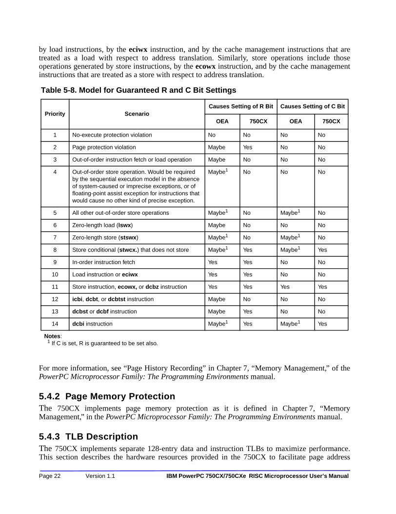
by load instructions, by the eciwx instruction, and by the cache management instructions that aretreated as a load with respect to address translation. Similarly, store operations include thoseoperations generated by store instructions, by the ecowx instruction, and by the cache managementinstructions that are treated as a store with respect to address translation.
For more information, see “Page History Recording” in Chapter 7, “Memory Management,” of thePowerPC Microprocessor Family: The Programming Environments manual.
5.4.2 Page Memory ProtectionThe 750CX implements page memory protection as it is defined in Chapter 7, “MemoryManagement,” in the PowerPC Microprocessor Family: The Programming Environments manual.
5.4.3 TLB Description The 750CX implements separate 128-entry data and instruction TLBs to maximize performance.This section describes the hardware resources provided in the 750CX to facilitate page address
Table 5-8. Model for Guaranteed R and C Bit Settings
Priority ScenarioCauses Setting of R Bit Causes Setting of C Bit
OEA 750CX OEA 750CX
1 No-execute protection violation No No No No
2 Page protection violation Maybe Yes No No
3 Out-of-order instruction fetch or load operation Maybe No No No
4 Out-of-order store operation. Would be required by the sequential execution model in the absence of system-caused or imprecise exceptions, or of floating-point assist exception for instructions that would cause no other kind of precise exception.
Maybe1 No No No
5 All other out-of-order store operations Maybe1 No Maybe1 No
6 Zero-length load (lswx) Maybe No No No
7 Zero-length store (stswx) Maybe1 No Maybe1 No
8 Store conditional (stwcx.) that does not store Maybe1 Yes Maybe1 Yes
9 In-order instruction fetch Yes Yes No No
10 Load instruction or eciwx Yes Yes No No
11 Store instruction, ecowx, or dcbz instruction Yes Yes Yes Yes
12 icbi, dcbt, or dcbtst instruction Maybe No No No
13 dcbst or dcbf instruction Maybe Yes No No
14 dcbi instruction Maybe1 Yes Maybe1 Yes
Notes: 1 If C is set, R is guaranteed to be set also.
Page 22 Version 1.1 IBM PowerPC 750CX/750CXe RISC Microprocessor User’s Manual

translation. Note that the hardware implementation of the MMU is not specified by the architecture,and while this description applies to the 750CX, it does not necessarily apply to other PowerPCprocessors.
5.4.3.1 TLB OrganizationBecause the 750CX has two MMUs (IMMU and DMMU) that operate in parallel, some of the MMUresources are shared, and some are actually duplicated (shadowed) in each MMU to maximizeperformance. For example, although the architecture defines a single set of segment registers for theMMU, the 750CX maintains two identical sets of segment registers, one for the IMMU and one forthe DMMU; when an instruction that updates the segment register executes, the 750CX automaticallyupdates both sets.
Each TLB contains 128 entries organized as a two-way set-associative array with 64 sets as shown inFigure 5-7 for the DTLB (the ITLB organization is the same). When an address is being translated, aset of two TLB entries is indexed in parallel with the access to a segment register. If the address inone of the two TLB entries is valid and matches the 40-bit virtual page number, that TLB entrycontains the translation. If no match is found, a TLB miss occurs.
Table of Contents 5/9/02 Page 23

Figure 5-7. Segment Register and DTLB Organization
T
0 7 8 31
0
15 T VSID
Segment Registers
VDTLB
0
63
V
EA[0–31]
EA[0–3]
EA[14–19]
VSID
Select
Compare
Compare
EA[4–13]
Line 1
Line 0
MUX
RPNLine1/Line 0 Hit
PA[0–19]
Page 24 Version 1.1 IBM PowerPC 750CX/750CXe RISC Microprocessor User’s Manual

Unless the access is the result of an out-of-order access, a hardware table search operation begins ifthere is a TLB miss. If the access is out of order, the table search operation is postponed until theaccess is required, at which point the access is no longer out of order. When the matching PTE isfound in memory, it is loaded into the TLB entry selected by the least-recently-used (LRU)replacement algorithm, and the translation process begins again, this time with a TLB hit.
To uniquely identify a TLB entry as the required PTE, the TLB entry also contains four more bits ofthe page index, EA[10–13] (in addition to the API bits in of the PTE).
Software cannot access the TLB arrays directly, except to invalidate an entry with the tlbieinstruction.
Each set of TLB entries has one associated LRU bit. The LRU bit for a set is updated any time eitherentry is used, even if the access is speculative. Invalid entries are always the first to be replaced.
Although both MMUs can be accessed simultaneously (both sets of segment registers and TLBs canbe accessed in the same clock), only one exception condition can be reported at a time. ITLB missexception conditions are reported when there are no more instructions to be dispatched or retired (thepipeline is empty), and DTLB miss exception conditions are reported when the load or storeinstruction is ready to be retired. Refer to Chapter 6, "Instruction Timing" in this manual for moredetailed information about the internal pipelines and the reporting of exceptions.
When an instruction or data access occurs, the effective address is routed to the appropriate MMU.EA0–EA3 select one of the 16 segment registers and the remaining effective address bits and theVSID field from the segment register is passed to the TLB. EA[14–19] then select two entries in theTLB; the valid bits are checked and the 40-bit virtual page number (24-bit VSID and EA[4–19]) mustmatch the VSID, EAPI, and API fields of the TLB entries. If one of the entries hits, the PP bits arechecked for a protection violation. If these bits don’t cause an exception, the C bit is checked and atable search operation is initiated if C must be updated. If C does not require updating, the RPN valueis passed to the memory subsystem and the WIMG bits are then used as attributes for the access.
Although address translation is disabled on a reset condition, the valid bits of TLB entries are notautomatically cleared. Thus, TLB entries must be explicitly cleared by the system software (with thetlbie instruction) before the valid entries are loaded and address translation is enabled. Also, note thatthe segment registers do not have a valid bit, and so they should also be initialized before translationis enabled.
Table of Contents 5/9/02 Page 25

5.4.3.2 TLB InvalidationThe 750CX implements the optional tlbie and tlbsync instructions, which are used to invalidate TLBentries. The execution of the tlbie instruction always invalidates four entries—both the ITLB andDTLB entries indexed by EA[14–19].
The architecture allows tlbie to optionally enable a TLB invalidate signaling mechanism in hardwareso that other processors also invalidate their resident copies of the matching PTE. The 750CX doesnot signal the TLB invalidation to other processors nor does it perform any action when a TLBinvalidation is performed by another processor.
The tlbsync instruction causes instruction execution to stop if the TLBISYNC signal is asserted. IfTLBISYNC is negated, instruction execution may continue or resume after the completion of atlbsync instruction. Section 8.9.2 on Page 8-39 describes the TLB synchronization mechanism infurther detail.
The tlbia instruction is not implemented on the 750CX and when its opcode is encountered, an illegalinstruction program exception is generated. To invalidate all entries of both TLBs, 64 tlbieinstructions must be executed, incrementing the value in EA14–EA19 by one each time.
(See Chapter 8, "Instruction Set" in the the PowerPC Microprocessor Family: The ProgrammingEnvironments manual for detailed information about this instruction.)
Software must ensure that instruction fetches or memory references to the virtual pages specified bythe tlbie have been completed prior to executing the tlbie instruction.
Other than the possible TLB miss on the next instruction prefetch, the tlbie instruction does not affectthe instruction fetch operation—that is, the prefetch buffer is not purged and does not cause theseinstructions to be refetched.
5.4.4 Page Address Translation SummaryFigure 5-8 provides the detailed flow for the page address translation mechanism.
The figure includes the checking of the N bit in the segment descriptor and then expands on the ‘TLBHit’ branch of Figure 5-6.
The detailed flow for the ‘TLB Miss’ branch of Figure 5-6 is described in Section 5.4.5 on Page 5-28.
NOTE: As in the case of block address translation, if an attempt is made to execute a dcbz instruction to a page marked either write-through or caching-inhibited (W = 1 or I = 1), an alignment exception is generated. The checking of memory protection violation conditions is described in Chapter 7, “Memory Management” in the PowerPC Microprocessor Family: The Programming Environments manual.
Page 26 Version 1.1 IBM PowerPC 750CX/750CXe RISC Microprocessor User’s Manual

Figure 5-8. Page Address Translation Flow—TLB Hit
(See The ProgrammingEnvironments
Manual)
(See Figure 5-9 on page 5-30)
(See The ProgrammingEnvironments Manual)
TLB Hit Case
Alignment Exception
Effective AddressGenerated
Continue Access to Memory Sub-system with WIMG-Bits from PTE
Page TableSearch Operation
PA[0–31]←RPN||A[20–31]
Page AddressTranslation
Check Page Memory Protection Violation Conditions
Instruction Fetch with N-BitSet in Segment Descriptor
(No-Execute)
Page Memory Protection Violation
Access Permitted
OtherwiseStore Access with
PTE [C] = 0
Otherwisedcbz Instructionwith W or I = 1
Otherwise
(See Figure 5-6 on page 5-14)
Generate 52-Bit Virtual Addressfrom Segment Descriptor
Compare Virtual Addresswith TLB Entries
Access Prohibited
Table of Contents 5/9/02
Page 27
5.4.5 Page Table Search OperationIf the translation is not found in the TLBs (a TLB miss), the 750CX initiates a table search operationwhich is described in this section. Formats for the PTE are given in “PTE Format for 32-BitImplementations,” in Chapter 7, “Memory Management” of the PowerPC Microprocessor Family:The Programming Environments manual.
The following is a summary of the page table search process performed by the 750CX.
1. The 32-bit physical address of the primary PTEG is generated as described in “Page Table Addresses” in Chapter 7, “Memory Management” of the PowerPC Microprocessor Family: The Programming Environments manual.
2. The first PTE (PTE0) in the primary PTEG is read from memory. PTE reads occur with an implied WIM memory/cache mode control bit setting of 0b001. Therefore, they are considered cacheable and read (burst) from memory and placed in the cache.
3. The PTE in the selected PTEG is tested for a match with the virtual page number (VPN) of the access. The VPN is the VSID concatenated with the page index field of the virtual address. For a match to occur, the following must be true:
— PTE[H] = 0
— PTE[V] = 1
— PTE[VSID] = VA[0–23]
— PTE[API] = VA[24–29]
4. If a match is not found, step 3 is repeated for each of the other seven PTEs in the primary PTEG. If a match is found, the table search process continues as described in step 8. If a match is not found within the 8 PTEs of the primary PTEG, the address of the secondary PTEG is generated.
5. The first PTE (PTE0) in the secondary PTEG is read from memory. Again, because PTE reads have a WIM bit combination of 0b001, an entire cache line is read into the on-chip cache.
6. The PTE in the selected secondary PTEG is tested for a match with the virtual page number (VPN) of the access. For a match to occur, the following must be true:
— PTE[H] = 1
— PTE[V] = 1
— PTE[VSID] = VA[0–23]
— PTE[API] = VA[24–29]
7. If a match is not found, step 6 is repeated for each of the other seven PTEs in the secondary PTEG. If it is never found, an exception is taken (step 9).
8. If a match is found, the PTE is written into the on-chip TLB and the R bit is updated in the PTE in memory (if necessary). If there is no memory protection violation, the C bit is also updated in memory (if the access is a write operation) and the table search is complete.
9. If a match is not found within the eight PTEs of the secondary PTEG, the search fails, and a page fault exception condition occurs (either an ISI exception or a DSI exception).
Page 28 Version 1.1 IBM PowerPC 750CX/750CXe RISC Microprocessor User’s Manual

Figure 5-9 and Figure 5-10 show how the conceptual model for the primary and secondary page tablesearch operations, described in the PowerPC Microprocessor Family: The ProgrammingEnvironments manual, are realized in the 750CX.
Figure 5-9 shows the case of a dcbz instruction that is executed with W = 1 or I = 1, and that the Rbit may be updated in memory (if required) before the operation is performed or the alignmentexception occurs. The R bit may also be updated if memory protection is violated.
Table of Contents 5/9/02 Page 29

Figure 5-9. Primary Page Table Search
(From Figure 5-10 on page 5-31)
Fetch PTE from PTEG
Otherwise
Perform SecondaryPage Table Search
Alignment ExceptionTLB[PTE[C]] ← 1
Generate PA Using Primary Hash FunctionPA ← Base PA of PTEG
PA ← PA+ 8(Fetch Next PTE in PTEG)
Fetch PTE (64-Bits)from PA
PTE [VSID, API, H, V] = Segment Descriptor [VSID], EA[API], 0, 1
PTE[C] ←1(Update PTE[C] in Memory)
Also Update PTE[R]in Memory if R_Flag = 1
PTE[R] ←1(Update PTE[R] in
Memory)
Last PTE in PTEG PTE[R] = 0
R_Flag = 1
Store Operationwith PTE[C] = 0
Otherwise
R_Flag = 1
PTE[R] ←1 (Update PTE[R] in Memory)
Primary PageTable Search
Write PTE into TLB
Otherwise
Secondary Page Table Search Hit
PTE[R] = 1
dcbz Instructionwith W or I = 1
Check Memory ProtectionViolation Conditions
R_Flag = 1
PTE[R] ←1 (Update PTE[R]
in Memory)
Otherwise
PTE[R] ← 1R_Flag ← 1
Memory ProtectionViolation
Page TableSearch Complete
Page TableSearch Complete
OtherwiseOtherwise
Access PermittedAccess Prohibited
Otherwise
Page 30 Version 1.1 IBM PowerPC 750CX/750CXe RISC Microproc
essor User’s Manual
Figure 5-10. Secondary Page Table Search Flow
The LSU initiates out-of-order accesses without knowledge of whether it is legal to do so. Therefore,the MMU does not perform hardware table search due to TLB misses until the request is required bythe program flow. In these out-of-order cases, the MMU does detect protection violations and whethera dcbz instruction specifies a page marked as write-through or cache-inhibited. The MMU alsodetects alignment exceptions caused by the dcbz instruction and prevents the changed bit in the PTEfrom being updated erroneously in these cases.
If an MMU register is being accessed by an instruction in the instruction stream, the IMMU stalls forone translation cycle to perform that operation. The sequencer serializes instructions to ensure thedata correctness. For updating the IBATs and SRs, the sequencer classifies those operations as fetchserializing. After such an instruction is dispatched, the instruction buffer is flushed and the fetch stallsuntil the instruction completes. However, for reading from the IBATs, the operation is classified asexecution serializing. As long as the LSU ensures that all previous instructions can be executed,subsequent instructions can be fetched and dispatched.
Page Fault (See Figure 5-10 on page 5-31)
Fetch PTE from PTEG
Otherwise
Generate PA Using Primary Hash FunctionPA ← Base PA of PTEG
PA ← PA+ 8(Fetch Next PTE in PTEG)
Fetch PTE (64-Bits)from PA
PTE [VSID, API, H, V] = Segment Descriptor [VSID], EA[API], 1, 1
Last PTE in PTEG
Secondary PageTable Search
Otherwise
Secondary Page Table Search Hit
ISI Exception DSI Exception
Set SRR1[1] = 1 Set DSISR[1] = 1
Instruction Access Data Access
Table of Contents
5/9/02 Page 31
5.4.6 Page Table UpdatesWhen TLBs are implemented (as in the 750CX) they are defined as noncoherent caches of the pagetables. TLB entries must be flushed explicitly with the TLB invalidate entry instruction (tlbie)whenever the corresponding PTE is modified. As the 750CX is intended primarily for uniprocessorenvironments, it does not provide coherency of TLBs between multiple processors. If the 750CX isused in a multiprocessor environment where TLB coherency is required, all synchronization must beimplemented in software.
Processors may write referenced and changed bits with unsynchronized, atomic byte store operations.Note that the V, R, and C bits each reside in a distinct byte of a PTE. Therefore, extreme care must betaken to use byte writes when updating only one of these bits.
Explicitly altering certain MSR bits (using the mtmsr instruction), or explicitly altering PTEs, orcertain system registers, may have the side effect of changing the effective or physical addresses fromwhich the current instruction stream is being fetched. This kind of side effect is defined as an implicitbranch. Implicit branches are not supported and an attempt to perform one causesboundedly-undefined results. Therefore, PTEs must not be changed in a manner that causes animplicit branch.
Chapter 2, “PowerPC Register Set” in the PowerPC Microprocessor Family: The ProgrammingEnvironments manual, lists the possible implicit branch conditions that can occur when systemregisters and MSR bits are changed.
5.4.7 Segment Register Updates Synchronization requirements for using the move to segment register instructions are described in“Synchronization Requirements for Special Registers and for Lookaside Buffers” in Chapter 2,“PowerPC Register Set” in the PowerPC Microprocessor Family: The Programming Environmentsmanual.
Page 32 Version 1.1 IBM PowerPC 750CX/750CXe RISC Microprocessor User’s Manual

Chapter 6 Instruction Timing6060
This chapter describes how the PowerPC 750CX microprocessor fetches, dispatches, and executesinstructions and how it reports the results of instruction execution. It gives detailed descriptions ofhow the 750CX’s execution units work, and how those units interact with other parts of the processor,such as the instruction fetching mechanism, register files, and caches. It gives examples of instructionsequences, showing potential bottlenecks and how to minimize their effects. Finally, it includes tablesthat identify the unit that executes each instruction implemented on the 750CX, the latency for eachinstruction, and other information that is useful for the assembly language programmer.
6.1 Terminology and ConventionsThis section provides an alphabetical glossary of terms used in this chapter. These definitions areprovided as a review of commonly used terms and as a way to point out specific ways these terms areused in this chapter.
• Branch prediction—The process of guessing whether a branch will or will not be taken. Such predictions can be correct or incorrect; the term ‘predicted’ as it is used here does not imply that the prediction is correct (successful). Instructions along the predicted path are fetch and dispatched to their respective execution units conditionally and can reach the completion unit. However, these instructions must first be validated by the branch resolution process before they can be retired. The PowerPC architecture defines a means for static branch prediction as part of the instruction encoding. The 750CX processor implements two types of dynamic branch prediction. See 6.4.1.2, "Branch Instructions and Completion".
• Branch resolution—The determination of the path that a branch instruction must take. If a branch prediction and branch resolution occur on the same cycle, it’s a no-brainer, the processor simply fetches instructions on the correct path as determined by the branch instruction. For predicted branches, branch resolution must determine if the prediction was correct. If the prediction was correct all speculatively fetched instructions that have been passed to their execution units are validated. If the prediction was wrong, the speculatively fetched instructions must be invalidated (flushed) and instruction fetching must resume along the other path for the branch instruction.
• Completion—Completion occurs when an instruction has finished executing and it results are stored in a rename register that had been allocated to it by the dispatch unit. These results are available to subsequent instructions or previously predicted branches.
• Dispatch—the process of moving an instruction from the instruction queue to an execution unit. In the 750CX processor the dispatch unit can process up to three instruction in a single cycle if one of the three is a branch. For the non-branch type instructions the dispatch must do a partial decode to determine the type of instruction inorder to pass it to it respective execution unit. Also, a rename register and a place in the completion queue must be reserved, otherwise a stall occurs. If a branch updates either LR or CTR register it also must be allocated to a completion queue entry.
• Fall-through —A not-taken branch.
• Fetch—The process of bringing instructions from the system memory (such as a cache or the main memory) into the instruction queue.
Table of Contents 5/9/02 Page 1

• Folding (branch folding)— On the 750CX, a branch is expunged from (folded out) the instruction queue via the dispatch mechanism, without either being passed to an execution unit and or given a position in the completion queue. Subsequent instructions are fetched from the target address calculated by the branch instruction, for branches taken or sequential instructions following the branch for a branch-not-taken, placed into a reservation register to which the instruction is dispatched.
• Finish—Finishing occurs in the last cycle of execution. (This could also be the first cycle of execution for instruction that only require one cycle for execution) In this cycle, the output rename register and the completion queue entry are updated to indicate that the instruction has finished executing.
• Latency— The number of clock cycles necessary to execute an instruction and make ready the results of that execution for a subsequent instruction.
• Pipeline—In the context of instruction timing, the term ‘pipeline’ refers to the interconnection of the stages. The events necessary to process an instruction are broken into several cycle-length tasks to allow work to be performed on several instructions simultaneously—analogous to an assembly line. As an instruction is processed, it passes from one stage to the next. When it does, the stage becomes available for the next instruction.
• Although an individual instruction may take many cycles to complete (the number of cycles is called instruction latency), pipelining makes it possible to overlap the processing so that the throughput (number of instructions completed per cycle) is greater than if pipelining were not implemented.
• Program order—The order of instructions in an executing program. More specifically, this term is used to refer to the original order in which program instructions are fetched into the instruction queue from the system memory.
• Rename register—Temporary buffers used to hold either source or destination values for instructions that are in a stage of execution. This simplifies the passing of data outside of the general purpose register file (GPR) between instructions during execution.
• Reservation station—A buffer between the dispatch and execute units where instructions await execution.
• Retirement—Removal of a completed instruction from the completion queue. At this time any output from the completed instruction is written to the appropriate architected destination register. This may be a GPR, FPR, or a CR field.
• Stage—The processing of instructions in the 750CX is done in stages. They are: fetch, decode/dispatch, execute, complete and retirement. The fetch unit brings instructions from the memory system into the instruction queue. Once in the instruction queue the dispatch unit must do a partial decode on the instruction to determine it’s type. If the instruction is an integer it is passed to the integer execution unit, if it is a floating-point type, it is passed to the floating-point execution unit, if it is a branch it is processed immediately by branch folding and branch prediction functions. Instructions spend one or more cycles in each stage as they are being processed by the 750CX processor.
• Stall—An occurrence when an instruction cannot proceed to the next stage. An instruction can spend multiple cycles in one stage. An integer multiply, for example, takes multiple cycles in the execute stage. When this occurs, subsequent instructions may stall.
Page 2 Version 1.1 IBM PowerPC 750CX/750CXe RISC Microprocessor User’s Manual

• Superscalar—A superscalar processor is one that has multiple execution units. The 750CX processor has one floating-point unit, two integer units, one load/store unit, and a system unit for miscellaneous instructions. PowerPC instructions are processed in parallel by these execution units.
• Throughput—A measure of the total number of instructions that are processed by all execution units per unit of time.
• Write-back—Write-back (in the context of instruction handling) occurs when a result is written into the architectural registers (typically the GPRs and FPRs). Results are written back at retirement time from rename registers for most instructions. The instruction is also removed from the completion queue at this time.
6.2 Instruction Timing OverviewThe 750CX design minimizes average instruction execution latency, the number of clock cycles ittakes to fetch, decode, dispatch, and execute instructions and make the results available for asubsequent instruction. Some instructions, such as loads and stores, access memory and requireadditional clock cycles between the execute phase and the write-back phase. These latencies varydepending on whether the access is to cacheable or noncacheable memory, whether it hits in the L1or L2 cache, whether the cache access generates a write-back to memory, whether the access causesa snoop hit from another device that generates additional activity, and other conditions that affectmemory accesses.
The 750CX implements many features to improve throughput, such as pipelining, superscalarinstruction issue, branch folding, two-level speculative branch handling, two types of branchprediction and multiple execution units that operate independently and in parallel.
As an instruction passes from stage to stage in a pipelined system, multiple instruction are in variousstages of execution at any given time. Also, with multiple execution units operating in parallel, morethen one instruction can be completed in a single cycle.
The 750CX contains the following execution units that operate independently and in parallel:
• Branch processing unit (BPU)
• Integer unit 1 (IU1)—executes all integer instructions
• Integer unit 2 (IU2)—executes all integer instructions except multiplies and divides
• 64-bit floating-point unit (FPU)
• Load/store unit (LSU)
• System register unit (SRU)
Figure 6-1 represents a generic pipelined execution unit.
Table of Contents 5/9/02 Page 3

Figure 6-1. Pipelined Execution Unit
The 750CX can retire two instructions on every clock cycle. In general, the 750CX processesinstructions in four stages—fetch, decode/dispatch, execute, and complete as shown in Figure 6-2.Note that the example of a pipelined execution unit in Figure 6-1 is similar to the three-stage FPUpipeline in Figure 6-2.
Figure 6-2. Superscalar/Pipeline Diagram
The instruction pipeline stages are described as follows.
• The instruction fetch stage includes the clock cycles necessary to request instructions from the memory system and the time the memory system takes to respond to the request. Instruction fetch timing depends on many variables, such as whether the instruction is in the branch target instruction cache, the L1 instruction cache, or the L2 cache. Those factors increase when it is necessary to fetch instructions from system memory, and include the processor-to-bus clock ratio, the amount of bus traffic, and whether any cache coherency operations are required.
Clock 0
Clock 1
Clock 2
Clock 3
Instruction A — —
Instruction B
Instruction C
Instruction D
Instruction A
Instruction B
Instruction C
—
Instruction A
Instruction B
Stage 1 Stage 2 Stage 3
Fetch
Complete (Write-back)
Decode/Dispatch
Execute Stage
FPU3SRU IU2IU1
Maximum three-instruction dispatchper clock cycle (includes one branchinstruction)
Maximum two -instruction completion per clock cycle
FPU2
FPU1
LSU1
Maximum four-instruction fetchper clock cycle
LSU2
BPU
Page 4 Version 1.1 IBM PowerPC 750CX/750CX
e RISC Microprocessor User’s Manual
Because there are so many variables, unless otherwise specified, the instruction timing examples below assume optimal performance, that the instructions are available in the instruction queue in the same clock cycle that they are requested. The fetch stage ends when the instruction is dispatched.
• The decode/dispatch stage consists of the time it takes to decode the instruction and dispatch it from the instruction queue to the appropriate execution unit. Instruction dispatch requires the following:
— Instructions can be dispatched only from the two lowest instruction queue entries, IQ0 and IQ1.
— A maximum of two instructions can be dispatched per clock cycle and one additional branch instruction can be handled by the BPU.
— Only one instruction can be dispatched to each execution unit per clock cycle.
— There must be a vacancy in the specified execution unit reservation station.
— A rename register must be available for each destination operand specified by the instruction.
— For an instruction to dispatch, the appropriate execution unit reservation station must be available and there must be an open position in the completion queue. If no entry is available, the instruction remains in the IQ.
• The execute stage consists of the time between dispatch to the execution unit (or reservation station) and the point at which the instruction vacates the execution unit.
Most integer instructions have a one-cycle latency; results of these instructions can be used in the clock cycle after an instruction enters the execution unit. However, integer multiply and divide instructions take multiple clock cycles to complete. The IU1 can process all integer instructions; the IU2 can process all integer instructions except multiply and divide instructions.
The LSU and FPU are pipelined (as shown in Figure 6-2).
• The complete (complete/write-back) pipeline stage maintains the correct architectural machine state and commits it to the architectural registers at the proper time. If the completion logic detects an instruction containing an exception status, all following instructions are cancelled, their execution results in rename registers are discarded, and the correct instruction stream is fetched.
The complete stage ends when the instruction is retired. Two instructions can be retired per cycle. Instructions are retired only from the two lowest completion queue entries, CQ0 and CQ1.
The notation conventions used in the instruction timing examples are as follows.
Fetch—The fetch stage includes the time between when an instruction is requested andwhen it is brought into the instruction queue. This latency can vary, depending upon whether theinstruction is in the BTIC, the L1 instruction cache, the L2 cache, or system memory (in which caselatency can be affected by bus speed and traffic on the system bus, and address translation issues).Therefore, in the examples in this chapters, the fetch stage is usually idealized, that is, an instructionis usually shown to be in the fetch stage when it is a valid instruction in the instruction queue. Theinstruction queue has six entries, IQ0–IQ5.
Table of Contents 5/9/02 Page 5

In dispatch entry (IQ0/IQ1)—Instructions can be dispatched from IQ0 and IQ1.Because dispatch is instantaneous, it is perhaps more useful to describe it as an event that marks thepoint in time between the last cycle in the fetch stage and the first cycle in the execute stage.
Execute—The operations specified by an instruction are being performed by theappropriate execution unit. The black stripe is a reminder that the instruction occupies an entry in thecompletion queue, described in Figure 6-3.
Complete—The instruction is in the completion queue. In the final stage, the results ofthe executed instruction are written back and the instruction is retired. The completion queue has sixentries, CQ0–CQ5.
In retirement entry—Completed instructions can be retired from CQ0 and CQ1. Likedispatch, retirement is an event that in this case occurs at the end of the final cycle of the completestage.
Figure 6-3 shows the stages of the 750CX’s execution units.
6.3 Timing ConsiderationsThe 750CX is a superscalar processor; as many as three instructions can be issued to the executionunits (one branch instruction to the branch processing unit, and two instructions issued from thedispatch queue to the other execution units) during each clock cycle. Only one instruction can bedispatched to each execution unit.
Although instructions appear to the programmer to execute in program order, the 750CX improvesperformance by executing multiple instructions at a time, using hardware to manage dependencies.When an instruction is dispatched, the register file or a rename register from a previous instructionprovides the source data to the execution unit. The register files and rename register have sufficientbandwidth to allow dispatch of two instructions per clock under most conditions.
Page 6 Version 1.1 IBM PowerPC 750CX/750CXe RISC Microprocessor User’s Manual

Figure 6-3. PowerPC 750CX Microprocessor Pipeline Stages
Fetch In Dispatch Execute1 Complete/Retire
Fetch In Dispatch Complete/RetireEA
Fetch In Dispatch Complete/Retire
IU1/IU2/SRU Instructions
LSU Instructions
FPU Instructions
NormalizeMultiply Add Round/
1 Several integer instructions, such as multiply and divide instructions, require multiple cycles in
Execute
Execute
CalculationCache Align
Entry
Entry
Entry
the execute stage.
BPU Instructions
Fetch FetchPredict
Complete/Retire2In DispatchEntry
In CompletionQueue2
2 Only those branch instructions that update the LR or CTR take an entry in the completion queue.
Table of Contents 5/9/02 Page 7

The 750CX’s BPU decodes and executes branches immediately after they are fetched. When aconditional branch cannot be resolved due to a CR data (or any) dependency, the branch direction ispredicted and execution continues on the predicted path. If the prediction is incorrect, the followingsteps are taken:
1. The instruction queue is purged and fetching continues from the correct path.
2. Any instructions behind (in program order) the predicted branch in the completion queue are allowed to complete.
3. Instructions fetched on the mispredicted path of the branch are purged.
4. Fetching resumes along the correct (other) path.
After an execution unit finishes executing an instruction, it places resulting data into the appropriateGPR or FPR rename register. The results are then stored into the correct GPR or FPR during thewrite-back stage (retirement). If a subsequent instruction needs the result as a source operand, it ismade available simultaneously to the appropriate execution unit, which allows a data-dependentinstruction to be decoded and dispatched without waiting to read the data from the register file.Branch instructions that update either the LR or CTR write back their results in a similar fashion.
The following section describes this process in greater detail.
6.3.1 General Instruction FlowAs many as four instructions can be fetched into the instruction queue (IQ) in a single clock cycle.Instructions enter the IQ and are issued to the various execution units from the dispatch queue. The750CX tries to keep the IQ full at all times, unless instruction cache throttling is operating.
The number of instructions requested in a clock cycle is determined by the number of vacant spacesin the IQ during the previous clock cycle. This is shown in the examples in this chapter. Although theinstruction queue can accept as many as four new instructions in a single clock cycle, if only one IQentry is vacant, only one instruction is fetched. Typically instructions are fetched from the L1instruction cache, but they may also be fetched from the branch target instruction cache (BTIC) if abranch is taken. If the branch taken instruction request hits in the BTIC, it can usually present the firsttwo instructions of the new instruction stream in the next clock cycle, giving enough time for the nextpair of instructions to be fetched from the instruction L1 cache resulting in no idle cycles in theinstruction stream (a.k.a., zero cycle branch). If instructions are not in the BTIC or the L1 instructioncache, they are fetched from the L2 cache or from system memory.
The 750CX’s instruction cache throttling feature, managed through the instruction cache throttlingcontrol (ICTC) register, can lower the processor’s overall junction temperature by slowing theinstruction fetch rate. See Chapter 10, "Power and Thermal Management" for more information.
Branch instructions are identified by the fetcher, and forwarded to the BPU directly, bypassing thedispatch queue. If the branch is unconditional or if the specified conditions are already known, thebranch can be resolved immediately. That is, the branch direction is known and instruction fetchingcan continue along the correct path. Otherwise, the branch direction must be predicted. The 750CXoffers several resources to aid in quick resolution of branch instructions and for improving theaccuracy of branch predictions. These include the following.
Page 8 Version 1.1 IBM PowerPC 750CX/750CXe RISC Microprocessor User’s Manual

• Branch target instruction cache—The 64-entry (four-way-associative) branch target instruction cache (BTIC) holds branch target instructions so when a branch is encountered in a repeated loop, usually the first two instructions in the target stream can be fetched into the instruction queue on the next clock cycle. The BTIC can be disabled and invalidated through bits in HID0. Coherency of the BTIC table is maintained by table reset on an icache flush invalidate, icbi or rfi instruction execution or when an exception is taken.
• Dynamic branch prediction—The 512-entry branch history table (BHT) is implemented with two bits per entry for four degrees of prediction—not-taken, strongly not-taken, taken, strongly taken. Whether a branch instruction is taken or not-taken can change the strength of the next prediction. This dynamic branch prediction is not defined by the PowerPC architecture.
To reduce aliasing, only predicted branches update the BHT entries. Dynamic branch prediction is enabled by setting HID0[BHT]; otherwise, static branch prediction is used.
• Static branch prediction—Static branch prediction is defined by the PowerPC architecture and involves encoding the branch instructions. See 6.4.1.3.1.”
Branch instructions that do not update the LR or CTR are removed from the instruction stream bybranch folding, as described in 6.4.1.1.” Branch instructions that update the LR or CTR are treated asif they require dispatch (even through they are not issued to an execution unit in the process). Theyare assigned a position in the completion queue to ensure that the CTR and LR are updated in correctprogram order.
All other instructions are issued from the IQ0 and IQ1. The dispatch rate depends upon theavailability of resources such as the execution units, rename registers, and completion queue entries,and upon the serializing behavior of some instructions. Instructions are dispatched in program order;an instruction in IQ1 cannot be dispatched ahead of one in IQ0.
6.3.2 Instruction Fetch TimingInstruction fetch latency depends on whether the fetch hits the BTIC, the L1 instruction cache, or theL2 cache. If no cache hit occurs, a memory transaction is required in which case fetch latency isaffected by bus traffic, bus clock speed, and memory translation. These issues are discussed furtherin the following sections.
6.3.2.1 Cache ArbitrationWhen the instruction fetcher requests instructions from the instruction cache, two things may happen.If the instruction cache is idle and the requested instructions are present, they are provided on the nextclock cycle. However, if the instruction cache is busy due to a cache-line-reload operation,instructions cannot be fetched until that operation completes.
6.3.2.2 Cache Hit If the instruction fetch hits the instruction cache, it takes only one clock cycle after the request for asmany as four instructions to enter the instruction queue. Note that the cache is not blocked to internalaccesses during a cache reload completes (hits under misses). The critical double word is writtensimultaneously to the cache and forwarded to the requesting unit, minimizing stalls due to loaddelays.
Table of Contents 5/9/02 Page 9

Figure 6-4 shows the paths taken by instructions.
Figure 6-4. Instruction Flow Diagram
SRUIU2
FPU
Complete (Retire)
Fetch
LSU
DispatchBranch
Instruction Queue
Completion Queue
Completion Queue
IU1
Store Queue
Processing Unit
(In program order)
Assignment
(In program order)
CQ5 CQ4 CQ3 CQ2 CQ1 CQ0
IQ5 IQ4 IQ3 IQ2 IQ1 IQ0
(Maximum 2 instructions per clock cycle; 1 instruction per unit)
(Maximum four instructions per clock cycle)
ReservationStations
Page 10 Version 1.1 IBM PowerPC 750CX/750CXe RISC Microprocessor User’s Manual

Figure 6-5 shows a simple example of instruction fetching that hits in the L1 cache. This example usesa series of integer add and double-precision floating-point add instructions to show how the numberof instructions to be fetched is determined, how program order is maintained by the instruction andcompletion queues, how instructions are dispatched and retired in pairs (maximum), and how theFPU, IU1, and IU2 pipelines function. The following instruction sequence is examined.
1 add2 fadd3 add4 fadd5 br 66 fsub7 fadd8 fadd9 add10 add11 add12 add13 fadd14 add15 fadd16 .17 .18 .
Table of Contents 5/9/02 Page 11

Figure 6-5. Instruction Timing—Cache Hit
The instruction timing for this example is described cycle-by-cycle as follows.
6 fadd
1 fadd
0 add
10 11
8 add
1 2 3 4 5 6 7 80
Fetch (in IQ)
In dispatch entry (IQ0/IQ1)
Execute2 add
3 fadd
9 add
4 b
10 add
11 add
12 fadd
9
7 fadd
•••
Complete (In CQ)
13 add
14 fadd
3
2
1
0
7
6
11
10
9
8
7
12
11
10
9
14
13
12
11
10
9
14
13
12
11
(16)
(15)
14
13
12
(17)
(16)
(15)
14
13
(18)
(17)
(16)
(15)
5
4
3
2
3
2
1
0
6
3
2
1
8
7
6
3
2
1
8
7
6
3
10
9
8
7
6
11
10
9
8
7
12
11
10
9
14
13
12
11
14
13
12
14
13
12
1
0
InstructionQueue
CompletionQueue
5 fsub
In retirement entry (CQ0/CQ1)
Page 12
Version 1 .1 IBM P owerPC 750CX/7 50CXe RISC Mic roproce ssor Use r’s Manual
1. In cycle 0, instructions 0–3 are fetched from the instruction cache. Instructions 0 and 1 are placed in the two entries in the instruction queue from which they can be dispatched on the next clock cycle.
2. In cycle 1, instructions 0 and 1 are dispatched to the IU2 and FPU, respectively. Notice that for instructions to be dispatched they must be assigned positions in the completion queue. In this case, since the completion queue was empty, instructions 0 and 1 take the two lowest entries in the completion queue. Instructions 2 and 3 drop into the two dispatch positions in the instruction queue. Because there were two positions available in the instruction queue in clock cycle 0, two instructions (4 and 5) are fetched into the instruction queue. Instruction 4 is a branch unconditional instruction, which resolves immediately as taken. Because the branch is taken, it can therefore be folded from the instruction queue.
3. In cycle 2, assume a BTIC hit occurs and target instructions 6 and 7 are fetched into the instruction queue, replacing the folded b instruction (4) and instruction 5. Instruction 0 completes, writes back its results and vacates the completion queue by the end of the clock cycle. Instruction 1 enters the second FPU execute stage, instruction 2 is dispatched to the IU2, and instruction 3 is dispatched into the first FPU execute stage. Because the taken branch instruction (4) does not update either CTR or LR, it does not require a position in the completion queue and can be folded.
4. In cycle 3, target instructions (6 and 7) are fetched, replacing instructions 4 and 5 in IQ0 and IQ1. This replacement on taken branches is called branch folding. Instruction 1 proceeds through the last of the three FPU execute stages. Instruction 2 has executed but must remain in the completion queue until instruction 1 completes. Instruction 3 replaces instruction 1 in the second stage of the FPU, and instruction 6 replaces instruction 3 in the first stage.
Because there were four vacancies in the instruction queue in the previous clock cycle, instructions 8–11 are fetched in this clock cycle.
5. Instruction 1 completes in cycle 4, allowing instruction 2 to complete. Instructions 3 and 6 continue through the FPU pipeline. Because there were two openings in the completion queue in the previous cycle, instructions 7 and 8 are dispatched to the FPU and IU2, respectively, filling the completion queue. Similarly, because there was one opening in the instruction queue in clock cycle 3, one instruction is fetched.
6. In cycle 5, instruction 3 completes, and instructions 13 and 14 are fetched. Instructions 6 and 7 continue through the FPU pipeline. No instructions are dispatched in this clock cycle because there were no vacant CQ entries in cycle 4.
7. In cycle 6, instruction 6 completes, instruction 7 is in stage 3 of the FPU execute stage, and although instruction 8 has executed, it must wait for instruction 7 to complete. The two integer instructions, 9 and 10, are dispatched to the IU2 and IU1, respectively. No instructions are fetched because the instruction queue was full on the previous cycle.
8. In cycle 7, instruction 7 completes, allowing instruction 8 to complete as well. Instructions 9 and 10 remain in the completion stage, since at most two instructions can complete in a cycle. Because there was one opening in the completion queue in cycle 6, instructions 11 is dispatched to the IU2. Two more instructions (15 and 16, which are shown only in the instruction queue) are fetched.
Table of Contents 5/9/02 Page 13

9. In cycle 8, instructions 9–11 are through executing. Instructions 9 and 10 complete, write back, and vacate the completion queue. Instruction 11 must wait to complete on the following cycle. Because the completion queue had one opening in the previous cycle, instruction 12 can be dispatched to the FPU. Similarly, the instruction queue had one opening in the previous cycle, so one additional instruction, 17, can be fetched.
10. In cycle 9, instruction 11 completes, instruction 12 continues through the FPU pipeline, and instructions 13 and 14 are dispatched. One new instruction, 18, can be fetched on this cycle because the instruction queue had one opening on the previous clock cycle.
6.3.2.3 Cache MissFigure 6-6 shows an instruction fetch that misses both the L1 cache and L2 cache. A processor/busclock ratio is 1:2 is used. The same instruction sequence is used as in Section 6.3.2.2, "Cache Hit",however in this example, the branch target instruction is not in either the L1 or L2 cache.
A cache miss, extends the latency of the fetch stage, so in this example, the fetch stage shownrepresents not only the time the instruction spends in the IQ, but the time required for the instructionto be loaded from system memory, beginning in clock cycle 2.
During clock cycle 3, the target instruction for the b instruction is not in the BTIC, the instructioncache or the L2 cache; therefore, a memory access must occur. During clock cycle 5, the address ofthe block of instructions is sent to the system bus. During clock cycle 7, two instructions (64 bits) arereturned from memory on the first beat and are forwarded both to the cache and the instruction fetcher.
Page 14 Version 1.1 IBM PowerPC 750CX/750CXe RISC Microprocessor User’s Manual

Figure 6-6. Instruction Timing—Cache Miss
6 fadd *
7 fadd *
1 fadd
0 add
10 11
8 add *
1 2 3 4 5 6 7 80
2 add
3 fadd
9 add *
4 b
10 add *
11 add *
12 fadd *
9
•••
3
2
1
0 7
9
8
5
4
3
2
3
2
1
0
3
2
1
3
2
1 3 6
7
6
9
8
7
6
1
0
InstructionQueue
CompletionQueue
5 fsubAddress
Data
Fetch *
In dispatch entry (IQ0/IQ1)
Execute
Complete (In CQ)
In retirement entry (CQ0/CQ1)
7
6
13 fadd *
* Instructions 5 and 6 are not in the IQ in clock cycle 5. Here, the fetch stage shows cache latency.
Table of C
ontents 5/9/02 Page 15
6.3.2.4 L2 Cache Access Timing Considerations If an instruction fetch misses both the BTIC and the L1 instruction cache, the 750CX next looks inthe L2 cache. If the requested instructions are there, they are burst into the 750CX in much the sameway as shown in Figure 6-6. The formula for the L2 cache latency for instruction accesses is asfollows.
1 processor clock + 3 L2 clocks + 1 processor clock
Therefore, since the L2 is operating in 1:1 mode, the instruction fetch takes 5 processor clock cycles.
6.3.2.5 Instruction Dispatch and Completion ConsiderationsSeveral factors affect the 750CX’s ability to dispatch instructions at a peak rate of two per cycle—theavailability of the execution unit, destination rename registers, and completion queue, as well as thehandling of completion-serialized instructions. Several of these limiting factors are illustrated in theprevious instruction timing examples.
To reduce dispatch unit stalls due to instruction data dependencies, the 750CX provides a single-entryreservation station for the FPU, SRU, and each IU, and a two-entry reservation station for the LSU.If a data dependency keeps an instruction from starting execution, that instruction is dispatched to thereservation station associated with its execution unit (and the rename registers are assigned), therebyfreeing the positions in the instruction queue so instructions can be dispatched to other executionunits. Execution begins during the same clock cycle that the rename buffer is updated with the datathe instruction is dependent on.
If both instructions in IQ0 and IQ1 require the same execution unit they must be executed sequentiallywhere IQ1 follows IQ0 through the execution unit. If these instructions require different executionunits, they can be dispatched on the same cycle, execute in parallel on separate execution units andcould complete together and be retired together on the same cycle.
The completion unit maintains program order after instructions are dispatched from the instructionqueue, guaranteeing in-order completion and a precise exception model. Completing an instructionimplies committing execution results to the architected destination registers. In-order completionensures the correct architectural state when the 750CX must recover from a mispredicted branch oran exception.
Instruction state and all information required for completion is kept in the six-entry, first-in/first-outcompletion queue. A completion queue entry is allocated for each instruction when it is dispatchedto an execute unit; if no entry is available, the dispatch unit stalls. A maximum of two instructions percycle may be completed and retired from the completion queue, and the flow of instructions can stallwhen a longer-latency instruction reaches the last position in the completion queue. Subsequentinstructions cannot be completed and retired until that longer-latency instruction completes andretires. Examples of this are shown in 6.3.2.2,” and 6.3.2.3.”
The 750CX can execute instructions out-of-order, but in-order completion by the completion unitensures a precise exception mechanism. Program-related exceptions are signaled when the instructioncausing the exception reaches the last position in the completion queue. By this time previousinstructions are retired.
Page 16 Version 1.1 IBM PowerPC 750CX/750CXe RISC Microprocessor User’s Manual

6.3.2.6 Rename Register OperationTo avoid contention for a given register file location in the course of out-of-order execution, the750CX provides rename registers for holding instruction results before the completion commits themto the architected register. There are six GPR rename registers, six FPR rename registers, and oneeach for the CR, LR, and CTR.
When the dispatch unit dispatches an instruction to its execution unit, it allocates a rename register(or registers) for the results of that instruction. If an instruction is dispatched to a reservation stationassociated with an execution unit due to a data dependency, the dispatcher also provides a tag to theexecution unit identifying the rename register that forwards the required data at completion. Whenthe source data reaches the rename register, execution can begin.
Instruction results are transferred from the rename registers to the architected registers by thecompletion unit when an instruction is retired from the completion queue, providing no exceptionsproceed it and also any predicted branch conditions have been resolved correctly. If a branchprediction was incorrect, the instructions fetched along the predicted path are flushed from thecompletion queue, and any results of those instructions are flushed from the rename registers.
6.3.2.7 Instruction SerializationAlthough the 750CX can dispatch and complete two instructions per cycle, so-called serializinginstructions limit dispatch and completion to one instruction per cycle. There are three types ofinstruction serialization:
• Execution serialization—Execution-serialized instructions are dispatched, held in the functional unit and do not execute until all prior instructions have completed. A functional unit holding an execution-serialized instruction will not accept further instructions from the dispatcher. For example, execution serialization is used for instructions that modify nonrenamed resources. Results from these instructions are generally not available or forwarded to subsequent instructions until the instruction completes (using mtspr to write to LR or CTR does provide forwarding to branch instructions).
• Completion serialization (also referred to as post-dispatch or tail serialization)—Completion-serialized instructions inhibit dispatching of subsequent instructions until the serialized instruction completes. Completion serialization is used for instructions that bypass the normal rename mechanism.
• Refetch serialization (flush serialization)—Refetch-serialized instructions inhibit dispatch of subsequent instructions and force refetching of subsequent instructions after completion.
Table of Contents 5/9/02 Page 17

6.4 Execution Unit TimingsThe following sections describe instruction timing considerations within each of the respectiveexecution units in the 750CX.
6.4.1 Branch Processing Unit Execution TimingFlow control operations (conditional branches, unconditional branches, and traps) are typicallyexpensive to execute in most machines because they disrupt normal flow in the instruction stream.When a change in program flow occurs, the IQ must be reloaded with the target instruction stream.Previously issued instructions will continue to execute while the new instruction stream makes itsway into the IQ, but depending on whether the target instruction is in the BTIC, instruction L1 cache,L2 cache, or in system memory, some opportunities may be missed to execute instructions, as theexample in Section 6.3.2.3, "Cache Miss" shows.
Performance features such as the branch folding, BTIC, dynamic branch prediction (implemented inthe BHT), two-level branch prediction, and the implementation of nonblocking caches minimize thepenalties associated with flow control operations on the 750CX. The timing for branch instructionexecution is determined by many factors including the following:
• Whether the branch is taken
• Whether instructions in the target stream, typically the first two instructions in the target stream, are in the branch target instruction cache (BTIC)
• Whether the target instruction stream is in the L1 cache
• Whether the branch is predicted
• Whether the prediction is correct
6.4.1.1 Branch Folding When a branch instruction is encountered by the fetcher, the BPU immediately begins to decode itand tries to resolve it. Branch folding is the removal of branches from the instruction stream. This isindependent of whether the branch is taken or not taken. However, if the branch instruction updateseither the LR or CTR it can not be removed and must be allocated a position in the completion queue.If a branch cannot be resolved, immediately, it is predicted and instruction fetching resumes along thepredicted path and those instructions are conditionally fed into the instruction queue. Later, if theprediction is finally resolved correct, the fetched instructions are validated and allowed to completeand be retired. If the prediction is resolved incorrect, instructions fetched are invalidated andinstruction fetching resumes along the other path of the branch.
Figure 6-7 shows branch folding. Here a br instruction is encountered in a series of add instructions.The branch is resolved as taken. What happens on the next clock cycle depends on whether the targetinstruction stream is in the BTIC, the instruction L1 cache, or if it must be fetched from the L2 cacheor from system memory.
Figure 6-7 shows cases where there is a BTIC hit, and when there is a BTIC miss (and instructioncache hit).
If there is a BTIC hit on the next clock cycle the b instruction is replaced by the target instruction,and1, that was found in the BTIC; the second and instruction is also fetched from the BTIC. On the
Page 18 Version 1.1 IBM PowerPC 750CX/750CXe RISC Microprocessor User’s Manual

next clock cycle, the next four and instructions from the target stream are fetched from the instructioncache.
If the target instruction is not in the BTIC, there is an idle cycle while the fetcher attempts to fetch thefirst four instructions from the instruction cache (on the next clock cycle). In the example in Figure6-7, the first four target instruction are fetched on the next clock.
If it misses in the BTIC or L1 caches, an L2 cache or memory access is required, the latency of whichis dependent on several factors, such as processor/bus clock ratios. In most cases, new instructionsarrive in the IQ before the execution units become idle.
Figure 6-7. Branch Taken
Figure 6-8 shows the removal of fall-through branch instructions, which occurs when a branch is nottaken or is predicted as not taken.
Figure 6-8. Removal of Fall-Through Branch Instruction
When a branch instruction is detected before it reaches a dispatch position, and if the branch iscorrectly predicted as taken, folding the branch instruction (and any instructions from the incorrectpath) reduces the latency required for flow control to zero; instruction execution proceeds as thoughthe branch was never there.
The advantage of removing the fall-through branch instructions at dispatch is only marginally lessthan that of branch folding. Because the branch is not taken, only the branch instruction needs to bediscarded. The only cost of expelling the branch instruction from one of the dispatch entries ratherthan folding it is missing a chance to dispatch an executable instruction from that position.
IQ5 add5
IQ4 add4
IQ3 add3IQ2 b
IQ1 add2
IQ0 add1
and2
and1
and6
and5
and4and3
Branch Folding(Taken Branch/BTIC Hit)
IQ5 add5IQ4 add4
IQ3 add3
IQ2 bIQ1 add2
IQ0 add1
and4
and3
and2and1
Branch Folding(Taken Branch/BTIC Miss)
Clock 0 Clock 1 Clock 2 Clock 0 Clock 1 Clock 2
IQ5 add5
IQ4 add4
IQ3 add3IQ2 b
IQ1 add2
IQ0 add1
add8
add7
add6add5
add4
add3
etc.
add9
add8add7
add6
add5
Branch Fall-Through(Not-Taken Branch)
Clock 0 Clock 1 Clock 2
Table of
Contents 5/9/02 Page 19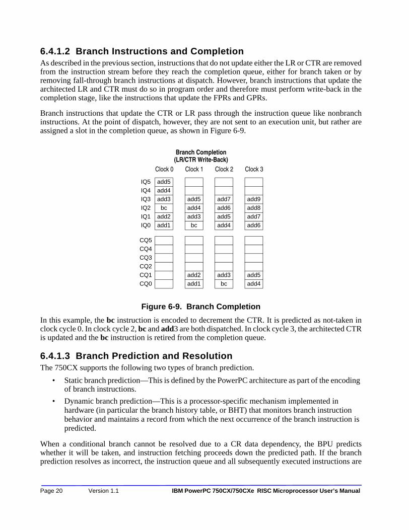
6.4.1.2 Branch Instructions and CompletionAs described in the previous section, instructions that do not update either the LR or CTR are removedfrom the instruction stream before they reach the completion queue, either for branch taken or byremoving fall-through branch instructions at dispatch. However, branch instructions that update thearchitected LR and CTR must do so in program order and therefore must perform write-back in thecompletion stage, like the instructions that update the FPRs and GPRs.
Branch instructions that update the CTR or LR pass through the instruction queue like nonbranchinstructions. At the point of dispatch, however, they are not sent to an execution unit, but rather areassigned a slot in the completion queue, as shown in Figure 6-9.
Figure 6-9. Branch Completion
In this example, the bc instruction is encoded to decrement the CTR. It is predicted as not-taken inclock cycle 0. In clock cycle 2, bc and add3 are both dispatched. In clock cycle 3, the architected CTRis updated and the bc instruction is retired from the completion queue.
6.4.1.3 Branch Prediction and Resolution The 750CX supports the following two types of branch prediction.
• Static branch prediction—This is defined by the PowerPC architecture as part of the encoding of branch instructions.
• Dynamic branch prediction—This is a processor-specific mechanism implemented in hardware (in particular the branch history table, or BHT) that monitors branch instruction behavior and maintains a record from which the next occurrence of the branch instruction is predicted.
When a conditional branch cannot be resolved due to a CR data dependency, the BPU predictswhether it will be taken, and instruction fetching proceeds down the predicted path. If the branchprediction resolves as incorrect, the instruction queue and all subsequently executed instructions are
IQ5 add5
IQ4 add4IQ3 add3
IQ2 bc
IQ1 add2IQ0 add1
add5
add4
add3bc
Branch Completion(LR/CTR Write-Back)
CQ5CQ4
CQ3
CQ2CQ1
CQ0
add2
add1
Clock 0 Clock 1
add7
add6
add5add4
add3
bc
Clock 2
add9
add8
add7add6
add5
add4
Clock 3
Page 20 Version 1.1
IBM PowerPC 750CX/75 0CXe RISC Microprocessor User’s Manual
purged, instructions executed prior to the predicted branch are allowed to complete, and instructionfetching resumes down the correct path.
The 750CX executes through two levels of prediction. Instructions from the first unresolved branchcan execute, but they cannot be retired until the branch is resolved. If a second branch instruction isencountered in the predicted instruction stream, it can be predicted and instructions can be fetched,but not executed, from the second branch. No action can be taken for a third branch instruction untilat least one of the two previous branch instructions is resolved.
The number of instructions that can be executed after the issue of a predicted branch instruction islimited by the fact that no instruction executed after a predicted branch may actually update (beretired) the register files or memory until the branch is resolved. That is, instructions may be issuedand executed, but cannot be retired from the completion unit. When an instruction following apredicted branch completes execution, it does not write back its results to the architected registers,instead, it stalls in the completion queue. Of course, when the completion queue is full, no additionalinstructions can be dispatched, even if an execution unit is idle.
In the case of a misprediction, the 750CX can easily redirect the instruction stream because theprogramming model has not been updated. When a branch is mispredicted, all instructions that weredispatched after the predicted branch instruction are flushed from the completion queue and anyresults are flushed from the rename registers.
The BTIC is a cache of two recently used instructions at the target (branch to address) of branchinstructions. If a taken-branch hits in the BTIC, two instructions are fed into the instruction queue onthe next cycle. If a taken-branch misses in the BTIC instruction fetching is done from the L1instruction cache. Coherency of the BTIC table is maintained by table reset on an icache flushinvalidate, icbi or rfi instruction execution or when an exception is taken.
In some situations, an instruction sequence creates dependencies that keep a branch instruction frombeing predicted because the address for the target of the branch is not available. This delays executionof the subsequent instruction stream. The instruction sequences and the resulting action of the branchinstruction are described as follows.
• An mtspr(LK) followed by a bclr—Fetching stops and the branch waits for the mtspr to execute.
• An mtspr(CTR) followed by a bcctr—Fetching stops and the branch waits for the mtspr to execute.
• An mtspr(CTR) followed by a bc (CTR decrement)—Fetching stops and the branch waits for the mtspr to execute.
• A third bc(based-on-CR) is encountered while there are two unresolved bc(based-on-CR). The third bc(based-on-CR) is not executed and fetching stops until one of the previous bc(based-on-CR) is resolved. (Note that branch conditions can be a function of the CTR and the CR; if the CTR condition is sufficient to resolve the branch, then a CR-dependency is ignored.)
Table of Contents 5/9/02 Page 21

6.4.1.3.1 Static Branch PredictionThe PowerPC architecture provides a field in branch instructions (the BO field) to allow software tospeculate (hint) whether a branch is likely to be taken. Rather than delaying instruction processinguntil the condition is known, the 750CX uses the instruction encoding to predict whether the branchis likely to be taken and begins fetching and executing along that path. When the branch condition isknown, the prediction is evaluated. If the prediction was correct, program flow continues along thatpath; otherwise, the processor flushes any instructions and their results from the mispredicted path,and program flow resumes along the correct path.
Static branch prediction is used when HID0[BHT] is cleared. That is, the branch history table, whichis used for dynamic branch prediction, is disabled.
For information about static branch prediction, see “Conditional Branch Control,” in Chapter 4,“Addressing Modes and Instruction Set Summary” in the PowerPC Microprocessor Family: TheProgramming Environments manual.
6.4.1.3.2 Predicted Branch Timing ExamplesFigure 6-10 shows cases where branch instructions are predicted. It shows how both taken andnot-taken branches are handled and how the 750CX handles both correct and incorrect predictions.The example shows the timing for the following instruction sequence:
0 add1 add2 bc3 mulhw4 bc T05 fadd 6 and
addT7 addT8 addT9 addT10 addT11 or
Page 22 Version 1.1 IBM PowerPC 750CX/750CXe RISC Microprocessor User’s Manual

Figure 6-10. Branch Instruction Timing
5 fadd
T3 add
4 bc
1 2 3 4 5 6 7 80 9 10
•••
•••
Fetch
In dispatch entry (IQ0/IQ1)
Predict
Execute
Complete (In CQ)
In retirement entry (CQ0/CQ1)
1 add
T2 add
3
2 (bc)
1
0
T1
T0
T5
T4
T3
T2
T5
T4
T3
T2
(8)
(7)
6
5
5
4
3
2
3
2
1
0
T1
T0
3
2
T1
T0
3
6
5
(8)
(7)
6
5
(8)
(7)
6
5
(8)
(7)
6
5
1
0
InstructionQueue
CompletionQueue
0 add
T1 add
T0 add
2 bc
3 mulhw
T5 or
T4 and
5 fadd *
6 and*
* Instructions 5 and 6 are not in the IQ in clock cycle 5. Here, the fetch stage shows cache latency.
Table of Con
tents 5/9 /02 Page 23
1. During clock cycle 0, instructions 0 and 1 are dispatched to their respective execution units. Instruction 2 is a branch instruction that updates the CTR. It is predicted as not taken in clock cycle 0. Instruction 3 is a mulhw instruction on which instruction 4 depends.
2. In clock cycle 1, instructions 2 and 3 enter the dispatch entries in the IQ. Instruction 4 (a second bc instruction) and 5 are fetched. The second bc instruction is predicted as taken. It can be folded, but it cannot be resolved until instruction 3 writes back.
3. In clock cycle 2, instruction 4 has been folded and instruction 5 has been flushed from the IQ. The two target instructions, T0 and T1, are both in the BTIC, so they are fetched in this cycle. Note that even though the first bc instruction may not have resolved by this point (we can assume it has), the 750CX allows fetching from a second predicted branch stream. However, these instructions could not be dispatched until the previous branch has resolved.
4. In clock cycle 3, target instructions T2–T5 are fetched as T0 and T1 are dispatched.
5. In clock cycle 4, instruction 3, on which the second branch instruction depended, writes back and the branch prediction is proven incorrect. Even though T0 is in CQ1, from which it could be written back, it is not written back because the branch prediction was incorrect. All target instructions are flushed from their positions in the pipeline at the end of this clock cycle, as are any results in the rename registers.
After one clock cycle required to refetch the original instruction stream, instruction 5, the sameinstruction that was fetched in clock cycle 1, is brought back into the IQ from the instruction cache,along with three others (not all of which are shown).
6.4.2 Integer Unit Execution TimingThe 750CX has two integer units. The IU1 can execute all integer instructions; and the IU2 canexecute all integer instructions except multiply and divide instructions. As shown in Figure 6-2, eachinteger unit has one execute pipeline stage, thus when a multicycle (e.g., divide) integer instruction isbeing executed, no additional integer instruction can begin to execute in that unit. However, the otherunit IU2 can continue to execute integer instructions. Table 6-6 lists integer instruction latencies.
Most integer instructions have an execution latency of one clock cycle.
6.4.3 Floating-Point Unit Execution TimingThe floating-point unit on the 750CX executes all floating-point instructions. Execution of mostfloating-point instructions is pipelined within the FPU, allowing up to three instructions to beexecuting in the FPU concurrently. While most floating-point instructions execute with three- orfour-cycle latency, and one- or two-cycle throughput, two instructions (fdivs and fdiv) execute withlatencies of 11 to 33 cycles. The fdivs, fdiv, mtfsb0, mtfsb1, mtfsfi, mffs, and mtfsf instructionsblock the floating-point unit pipeline until they complete execution, and thereby inhibit the dispatchof additional floating-point instructions. See Table 6-7 for floating-point instruction execution timing.
6.4.4 Effect of Floating-Point Exceptions on PerformanceFor the fastest and most predictable floating-point performance, all exceptions should be disabled inthe FPSCR and MSR.
Page 24 Version 1.1 IBM PowerPC 750CX/750CXe RISC Microprocessor User’s Manual

6.4.5 Load/Store Unit Execution TimingThe execution of most load and store instructions is pipelined. The LSU has two pipeline stages. Thefirst is for effective address calculation and MMU translation and the second is for accessing data inthe cache. Load and store instructions have a two-cycle latency and one-cycle throughput. Forinstructions that store FPR values (stfd, stfs, and their variations), the data to be stored is prefetchedfrom the source register during the first pipeline stage. In cases where this register is updated thatsame cycle, the instruction will stall to get the correct data, resulting in one additional cycle of latency.
If operands are misaligned, additional latency may be required either for an alignment exception tobe taken or for additional bus accesses. Load instructions that miss in the cache, block subsequentcache accesses during the cache line refill. Table 6-8 gives load and store instruction executionlatencies.
6.4.6 Effect of Operand Placement on PerformanceThe PowerPC VEA states that the placement (location and alignment) of operands in memory mayaffect the relative performance of memory accesses, and in some cases affect it significantly. Theeffects memory operand placement has on performance are shown in Table 6-1.
The best performance is guaranteed if memory operands are aligned on natural boundaries. For thebest performance across the widest range of implementations, the programmer should assume theperformance model described in Chapter 3, “Operand Conventions” in the PowerPC MicroprocessorFamily: The Programming Environments manual.
The effect of misalignment on memory access latency is the same for big- and little-endian addressingmodes except for multiple and string operations that cause an alignment exception in little-endianmode.
Table 6-1. Performance Effects of Memory Operand Placement
Operand Boundary Crossing
Size Byte Alignment None 8 Byte Cache Block Protection Boundary
Integer
4 byte 4 Optimal1 — — —
< 4 Optimal Good Good Good
2 byte 2 Optimal — — —
< 2 Optimal Good Good Good
1 byte 1 Optimal — — —
lmw,stmw2
4 Good 3 Good Good Good
< 4 Poor 4 Poor Poor Poor
String 2 — Good Good Good Good
Floating-Point
Table of Contents 5/9/02 Page 25

6.4.7 Integer Store GatheringThe 750CX performs store gathering for write-through operations to nonguarded space. It performscache-inhibited stores to nonguarded space for 4-byte, word-aligned stores. These stores arecombined in the LSU to form a double word and are sent out on the 60x bus as a single-beat operation.However, stores are gathered only if the successive stores meet the criteria and are queued andpending. Store gathering occurs regardless of the address order of the stores. Store gathering isenabled by setting HID0[SGE]. Stores can be gathered in both endian modes.
Store gathering is not done for the following:
• Cacheable store operations
• Stores to guarded cache-inhibited or write-through space
• Byte-reverse store operations
• stwcx. instructions
• ecowx instructions
• A store that occurs during a table search operation
• Floating-point store operations
If store gathering is enabled and the stores do not fall under the above categories, an eieio or syncinstruction must be used to prevent two stores from being gathered.
6.4.8 System Register Unit Execution TimingMost instructions executed by the SRU either directly access renamed registers or access or modifynonrenamed registers. They generally execute in a serial manner. Results from these instructions arenot available to subsequent instructions until the instruction completes and is retired. See 6.3.2.7,” formore information on serializing instructions executed by the SRU, and refer to Table 6-4 andTable 6-5 for SRU instruction execution timings.
8 byte 8 Optimal — — —
4 — Good Good Good
< 4 — Poor Poor Poor
4 byte 4 Optimal — — —
< 4 Poor Poor Poor Poor
Notes:1 Optimal means one EA calculation occurs.2 Not supported in little-endian mode, causes an alignment exception.3 Good means multiple EA calculations occur that may cause additional bus activities with multiple bus transfers.4 Poor means that an alignment exception occurs.
Table 6-1. Performance Effects of Memory Operand Placement
Operand Boundary Crossing
Size Byte Alignment None 8 Byte Cache Block Protection Boundary
Page 26 Version 1.1 IBM PowerPC 750CX/750CXe RISC Microprocessor User’s Manual

6.5 Memory Performance ConsiderationsBecause the 750CX can have a maximum instruction throughput of three instructions per clock cycle,lack of memory bandwidth can affect performance. For the 750CX to maximize performance, it mustbe able to read and write data efficiently. If a system has multiple bus devices, one of them mayexperience long memory latencies while another bus master (for example, a direct-memory accesscontroller) is using the external bus.
6.5.1 Caching and Memory CoherencyTo minimize the effect of bus contention, the PowerPC architecture defines WIM bits that are used toconfigure memory regions as caching-enforced or caching-inhibited. Accesses to such memorylocations never update the L1 cache. If a cache-inhibited access hits the L1 cache, the cache block isinvalidated. If the cache block is marked modified, it is copied back to memory before beinginvalidated. Where caching is permitted, memory is configured as either write-back or write-through,which are described as follows:
• Write-back— Configuring a memory region as write-back lets a processor modify data in the cache without updating system memory. For such locations, memory updates occur only on modified cache block replacements, cache flushes, or when one processor needs data that is modified in another’s cache. Therefore, configuring memory as write-back can help when bus traffic could cause bottlenecks, especially for multiprocessor systems and for regions in which data, such as local variables, is used often and is coupled closely to a processor.
If multiple devices use data in a memory region marked write-through, snooping must be enabled to allow the copy-back and cache invalidation operations necessary to ensure cache coherency. The 750CX’s snooping hardware keeps other devices from accessing invalid data. For example, when snooping is enabled, the 750CX monitors transactions of other bus devices. For example, if another device needs data that is modified on the 750CX’s cache, the access is delayed so the 750CX can copy the modified data to memory.
• Write-through—Store operations to memory marked write-through always update both system memory and the L1 cache on cache hits. Because valid cache contents always match system memory marked write-through, cache hits from other devices do not cause modified data to be copied back as they do for locations marked write-back. However, all write operations are passed to the bus, which can limit performance. Load operations that miss the L1 cache must wait for the external store operation.
Write-through configuration is useful when cached data must agree with external memory (for example, video memory), when shared (global) data may be needed often, or when it is undesirable to allocate a cache block on a cache miss.
Chapter 3, "The 750CX Instruction and Data Cache Operation" describes the caches, memoryconfiguration, and snooping in detail.
Table of Contents 5/9/02 Page 27

6.5.2 Effect of TLB Miss If a page address translation is not in a TLB, the 750CX hardware searches the page tables andupdates the TLB when a translation is found. Table 6-2 shows the estimated latency for the hardwareTLB load for different cache configurations and conditions.
The PTE table search assumes a hit in the first entry of the primary PTEG.
6.6 Instruction Scheduling GuidelinesThe performance of the 750CX can be improved by avoiding resource conflicts and schedulinginstructions to take fullest advantage of the parallel execution units. Instruction scheduling on the750CX can be improved by observing the following guidelines.
• To reduce mispredictions, separate the instruction that sets CR bits from the branch instruction that evaluates them. Because there can be no more than 12 instructions in the processor (with the instruction that sets CR in CQ0 and the dependent branch instruction in IQ5), there is no advantage to having more than 10 instructions between them.
• Likewise, when branching to a location specified by the CTR or LR, separate the mtspr instruction that initializes the CTR or LR from the dependent branch instruction. This ensures the register values are available sooner to the branch instruction.
• Schedule instructions such that two can be dispatched at a time.
• Schedule instructions to minimize stalls due to execution units being busy.
• Avoid scheduling high-latency instructions close together. Interspersing single-cycle latency integer instructions between longer-latency instructions minimizes the effect that instructions such as integer divide and multiply can have on throughput.
• Avoid using serializing instructions.
• Schedule instructions to avoid dispatch stalls.
— Six instructions can be tracked in the completion queue; therefore, only six instructions can be in the execute stages at any one time.
— There are six GPR rename registers; therefore only six GPRs can be specified as destination operands at any time. If no rename registers are available, instructions cannot enter the execute stage and remain in the reservation station or instruction queue until they become available.
NOTE: Load with update address instructions use two rename registers.
Table 6-2. TLB Miss Latencies
L1 Condition (Instruction and Data)
L2 Condition Processor/System Bus
Clock RatioEstimated Latency
(Cycles)
100% cache hit — — 7
100% cache miss 100% cache hit — 13
100% cache miss 100% cache miss 2.5:1 (6:3:3:3 memory) 62
100% cache miss 100% cache miss 4:1 (5:2:2:2 memory) 77
Page 28 Version 1.1 IBM PowerPC 750CX/750CXe RISC Microprocessor User’s Manual

— Similarly, there are six FPR rename registers, so only six FPR destination operands can be in the execute and complete stages at any time.
6.6.1 Branch, Dispatch, and Completion Unit Resource RequirementsThis section describes the specific resources required to avoid stalls during branch resolution,instruction dispatching, and instruction completion.
6.6.1.1 Branch Resolution Resource RequirementsThe following is a list of branch instructions and the resources required to avoid stalling the fetch unitin the course of branch resolution:
• The bclr instruction requires LR availability.
• The bcctr instruction requires CTR availability.
• Branch and link instructions require shadow LR availability.
• The “branch conditional on counter decrement and the CR” condition requires CTR availability or the CR condition must be false, and the 750CX cannot execute instructions after an unresolved predicted branch when the BPU encounters a branch.
• A branch conditional on CR condition cannot be executed following an unresolved predicted branch instruction.
6.6.1.2 Dispatch Unit Resource RequirementsThe following is a list of resources required to avoid stalls in the dispatch unit. IQ[0] and IQ[1] arethe two dispatch entries in the instruction queue:
• Requirements for dispatching from IQ[0] are as follows.
— Needed execution unit available
— Needed GPR rename registers available
— Needed FPR rename registers available
— Completion queue is not full.
— A completion-serialized instruction is not being executed.
• Requirements for dispatching from IQ[1] are as follows.
— Instruction in IQ[0] must dispatch.
— Instruction dispatched by IQ[0] is not completion- or refetch-serialized.
— Needed execution unit is available (after dispatch from IQ[0]).
— Needed GPR rename registers are available (after dispatch from IQ[0]).
— Needed FPR rename register is available (after dispatch from IQ[0]).
— Completion queue is not full (after dispatch from IQ[0]).
Table of Contents 5/9/02 Page 29

6.6.1.3 Completion Unit Resource RequirementsThe following is a list of resources required to avoid stalls in the completion unit; note that the twocompletion entries are described as CQ[0] and CQ[1], where CQ[0] is the completion queue locatedat the end of the completion queue (see Figure 6-4).
• Requirements for completing an instruction from CQ[0] are as follows:
— Instruction in CQ[0] must be finished.
— Instruction in CQ[0] must not follow an unresolved predicted branch.
— Instruction in CQ[0] must not cause an exception.
• Requirements for completing an instruction from CQ[1] are as follows:
— Instruction in CQ[0] must complete in same cycle.
— Instruction in CQ[1] must be finished.
— Instruction in CQ[1] must not follow an unresolved predicted branch.
— Instruction in CQ[1] must not cause an exception.
— Instruction in CQ[1] must be an integer or load instruction.
— Number of CR updates from both CQ[0] and CQ[1] must not exceed two.
— Number of GPR updates from both CQ[0] and CQ[1] must not exceed two.
— Number of FPR updates from both CQ[0] and CQ[1] must not exceed two.
Page 30 Version 1.1 IBM PowerPC 750CX/750CXe RISC Microprocessor User’s Manual

6.7 Instruction Latency SummaryTable 6-3 through Table 6-8 on Page 6-36 list the latencies associated with instructions executed byeach execution unit. Table 6-3 describes branch instruction latencies.
Table 6-4 lists system register instruction latencies.
Table 6-3. Branch Instructions
Mnemonic Primary Extended Latency
b[l][a] 18 — Unless these instructions update either the CTR or the LR, branch operations are folded if they are either taken or predicted as taken. They fall through if they are not taken or predicted as not taken.bc[l][a] 16 —
bcctr[l] 19 528
bclr[l] 19 16
Table 6-4. System Register Instructions
Mnemonic Primary Extended Unit Cycles Serialization
eieio 31 854 SRU 1 —
isync 19 150 SRU 2 Completion, refetch
mfmsr 31 83 SRU 1 —
mfspr (DBATs) 31 339 SRU 3 Execution
mfspr (IBATs) 31 339 SRU 3 —
mfspr (not I/DBATs) 31 339 SRU 1 Execution
mfsr 31 595 SRU 3 —
mfsrin 31 659 SRU 3 Execution
mftb 31 371 SRU 1 —
mtmsr 31 146 SRU 1 Execution
mtspr (DBATs) 31 467 SRU 2 Execution
mtspr (IBATs) 31 467 SRU 2 Execution
mtspr (not I/DBATs) 31 467 SRU 2 Execution
mtsr 31 210 SRU 2 Execution
mtsrin 31 242 SRU 2 Execution
mttb 31 467 SRU 1 Execution
rfi 19 50 SRU 2 Completion, refetch
sc 17 - -1 SRU 2 Completion, refetch
sync 31 598 SRU 31
1 This assumes no pending stores in the store queue. If there are, the sync completes after they complete to memory. If broadcast is enabled on the 60x bus, sync completes only after a successful broadcast.
—
tlbsync 2 31 566 — —
Notes:
Table of Contents 5/9/02 Page 31

Table 6-5 lists condition register logical instruction latencies.
Table 6-6 shows integer instruction latencies. Note that the IU1 executes all integer arithmeticinstructions—multiply, divide, shift, rotate, add, subtract, and compare. The IU2 executes all integerinstructions except multiply and divide (that is, shift, rotate, add, subtract, and compare).
2 tlbsync is dispatched only to the completion buffer (not to any execution unit) and is marked finished as it is dispatched. Upon retirement, it waits for an external TLBISYNC signal to be asserted. In most systems TLBISYNC is always asserted so the instruction is a no-op.
Table 6-5. Condition Register Logical Instructions
Mnemonic Primary Extended Unit Cycles Serialization
crand 19 257 SRU 1 Execution
crandc 19 129 SRU 1 Execution
creqv 19 289 SRU 1 Execution
crnand 19 225 SRU 1 Execution
crnor 19 33 SRU 1 Execution
cror 19 449 SRU 1 Execution
crorc 19 417 SRU 1 Execution
crxor 19 193 SRU 1 Execution
mcrf 19 0 SRU 1 Execution
mcrxr 31 512 SRU 1 Execution
mfcr 31 19 SRU 1 Execution
mtcrf 31 144 SRU 1 Execution
Page 32 Version 1.1 IBM PowerPC 750CX/750CXe RISC Microprocessor User’s Manual

Table 6-6. Integer Instructions
Mnemonic Primary Extended Unit Cycles Serialization
addc[o][.] 31 10 IU1/IU2 1 —
adde[o][.] 31 138 IU1/IU2 1 Execution
addi 14 — IU1/IU2 1 —
addic 12 — IU1/IU2 1 —
addic. 13 — IU1/IU2 1 —
addis 15 — IU1/IU2 1 —
addme[o][.] 31 234 IU1/IU2 1 Execution
addze[o][.] 31 202 IU1/IU2 1 Execution
add[o][.] 31 266 IU1/IU2 1 —
andc[.] 31 60 IU1/IU2 1 —
andi. 28 — IU1/IU2 1 —
andis. 29 — IU1/IU2 1 —
and[.] 31 28 IU1/IU2 1 —
cmp 31 0 IU1/IU2 1 —
cmpi 11 — IU1/IU2 1 —
cmpl 31 32 IU1/IU2 1 —
cmpli 10 — IU1/IU2 1 —
cntlzw[.] 31 26 IU1/IU2 1 —
divwu[o][.] 31 459 IU1 19 —
divw[o][.] 31 491 IU1 19 —
eqv[.] 31 284 IU1/IU2 1 —
extsb[.] 31 954 IU1/IU2 1 —
extsh[.] 31 922 IU1/IU2 1 —
mulhwu[.] 31 11 IU1 2,3,4,5,6 —
mulhw[.] 31 75 IU1 2,3,4,5 —
mulli 7 — IU1 2,3 —
mullw[o][.] 31 235 IU1 2,3,4,5 —
nand[.] 31 476 IU1/IU2 1 —
neg[o][.] 31 104 IU1/IU2 1 —
nor[.] 31 124 IU1/IU2 1 —
Table of Contents 5/9/02 Page 33

Table 6-7 shows latencies for floating-point instructions. Pipelined floating-point instructions areshown with number of clocks in each pipeline stage separated by dashes. Floating-point instructionswith a single entry in the cycles column are not pipelined; when the FPU executes these nonpipelinedinstructions, it remains busy for the full duration of the instruction execution and is not available forsubsequent instructions.
orc[.] 31 412 IU1/IU2 1 —
ori 24 — IU1/IU2 1 —
oris 25 — IU1/IU2 1 —
or[.] 31 444 IU1/IU2 1 —
rlwimi[.] 20 — IU1/IU2 1 —
rlwinm[.] 21 — IU1/IU2 1 —
rlwnm[.] 23 — IU1/IU2 1 —
slw[.] 31 24 IU1/IU2 1 —
srawi[.] 31 824 IU1/IU2 1 —
sraw[.] 31 792 IU1/IU2 1 —
srw[.] 31 536 IU1/IU2 1 —
subfc[o][.] 31 8 IU1/IU2 1 —
subfe[o][.] 31 136 IU1/IU2 1 Execution
subfic 8 — IU1/IU2 1 —
subfme[o][.] 31 232 IU1/IU2 1 Execution
subfze[o][.] 31 200 IU1/IU2 1 Execution
subf[.] 31 40 IU1/IU2 1 —
tw 31 4 IU1/IU2 2 —
twi 3 — IU1/IU2 2 —
xori 26 — IU1/IU2 1 —
xoris 27 — IU1/IU2 1 —
xor[.] 31 316 IU1/IU2 1 —
Table 6-6. Integer Instructions (Continued)
Mnemonic Primary Extended Unit Cycles Serialization
Page 34 Version 1.1 IBM PowerPC 750CX/750CXe RISC Microprocessor User’s Manual

Table 6-7. Floating-Point Instructions
Mnemonic Primary Extended Unit Cycles Serialization
fabs[.] 63 264 FPU 1-1-1 —
fadds[.] 59 21 FPU 1-1-1 —
fadd[.] 63 21 FPU 1-1-1 —
fcmpo 63 32 FPU 1-1-1 —
fcmpu 63 0 FPU 1-1-1 —
fctiwz[.] 63 15 FPU 1-1-1 —
fctiw[.] 63 14 FPU 1-1-1 —
fdivs[.] 59 18 FPU 17 —
fdiv[.] 63 18 FPU 31 —
fmadds[.] 59 29 FPU 1-1-1 —
fmadd[.] 63 29 FPU 2-1-1 —
fmr[.] 63 72 FPU 1-1-1 —
fmsubs[.] 59 28 FPU 1-1-1 —
fmsub[.] 63 28 FPU 2-1-1 —
fmuls[.] 59 25 FPU 1-1-1 —
fmul[.] 63 25 FPU 2-1-1 —
fnabs[.] 63 136 FPU 1-1-1 —
fneg[.] 63 40 FPU 1-1-1 —
fnmadds[.] 59 31 FPU 1-1-1 —
fnmadd[.] 63 31 FPU 2-1-1 —
fnmsubs[.] 59 30 FPU 1-1-1 —
fnmsub[.] 63 30 FPU 2-1-1 —
fres[.] 59 24 FPU 2-1-1 —
frsp[.] 63 12 FPU 1-1-1 —
frsqrte[.] 63 26 FPU 2-1-1 —
fsel[.] 63 23 FPU 1-1-1 —
fsubs[.] 59 20 FPU 1-1-1 —
fsub[.] 63 20 FPU 1-1-1 —
mcrfs 63 64 FPU 1-1-1 Execution
mffs[.] 63 583 FPU 1-1-1 Execution
Table of Contents 5/9/02 Page 35

Table 6-8 shows load and store instruction latencies. Pipelined load/store instructions are shown withcycles of total latency and throughput cycles separated by a colon.
mtfsb0[.] 63 70 FPU 3 —
mtfsb1[.] 63 38 FPU 3 —
mtfsfi[.] 63 134 FPU 3 —
mtfsf[.] 63 711 FPU 3 —
Table 6-8. Load and Store Instructions
Mnemonic Primary Extended Unit Cycles Serialization
dcbf 31 86 LSU 3:51 Execution
dcbi 31 470 LSU 3:31 Execution
dcbst 31 54 LSU 3:51 Execution
dcbt 31 278 LSU 2:1 —
dcbtst 31 246 LSU 2:1 —
dcbz 31 1014 LSU 3:61, 2 Execution
eciwx 31 310 LSU 2:1 —
ecowx 31 438 LSU 2:1 —
icbi 31 982 LSU 3:41 Execution
lbz 34 — LSU 2:1 —
lbzu 35 — LSU 2:1 —
lbzux 31 119 LSU 2:1 —
lbzx 31 87 LSU 2:1 —
lfd 50 — LSU 2:1 —
lfdu 51 — LSU 2:1 —
lfdux 31 631 LSU 2:1 —
lfdx 31 599 LSU 2:1 —
lfs 48 — LSU 2:1 —
lfsu 49 — LSU 2:1 —
lfsux 31 567 LSU 2:1 —
lfsx 31 535 LSU 2:1 —
lha 42 — LSU 2:1 —
Table 6-7. Floating-Point Instructions (Continued)
Mnemonic Primary Extended Unit Cycles Serialization
Page 36 Version 1.1 IBM PowerPC 750CX/750CXe RISC Microprocessor User’s Manual

lhau 43 — LSU 2:1 —
lhaux 31 375 LSU 2:1 —
lhax 31 343 LSU 2:1 —
lhbrx 31 790 LSU 2:1 —
lhz 40 — LSU 2:1 —
lhzu 41 — LSU 2:1 —
lhzux 31 311 LSU 2:1 —
lhzx 31 279 LSU 2:1 —
lmw 46 — LSU 2 + n 3 Completion, execution
lswi 31 597 LSU 2 + n 3 Completion, execution
lswx 31 533 LSU 2 + n 3 Completion, execution
lwarx 31 20 LSU 3:1 Execution
lwbrx 31 534 LSU 2:1 —
lwz 32 — LSU 2:1 —
lwzu 33 — LSU 2:1 —
lwzux 31 55 LSU 2:1 —
lwzx 31 23 LSU 2:1 —
stb 38 — LSU 2:1 —
stbu 39 — LSU 2:1 —
stbux 31 247 LSU 2:1 —
stbx 31 215 LSU 2:1 —
stfd 54 — LSU 2:1 —
stfdu 55 — LSU 2:1 —
stfdux 31 759 LSU 2:1 —
stfdx 31 727 LSU 2:1 —
stfiwx 31 983 LSU 2:1 —
stfs 52 — LSU 2:1 —
stfsu 53 — LSU 2:1 —
stfsux 31 695 LSU 2:1 —
stfsx 31 663 LSU 2:1 —
sth 44 — LSU 2:1 —
Table 6-8. Load and Store Instructions (Continued)
Mnemonic Primary Extended Unit Cycles Serialization
Table of Contents 5/9/02 Page 37

sthbrx 31 918 LSU 2:1 —
sthu 45 — LSU 2:1 —
sthux 31 439 LSU 2:1 —
sthx 31 407 LSU 2:1 —
stmw 47 — LSU 2 + n 3 Execution
stswi 31 725 LSU 2 + n 3 Execution
stswx 31 661 LSU 2 + n 3 Execution
stw 36 — LSU 2:1 —
stwbrx 31 662 LSU 2:1 —
stwcx. 31 150 LSU 8:8 Execution
stwu 37 — LSU 2:1 —
stwux 31 183 LSU 2:1 —
stwx 31 151 LSU 2:1 —
tlbie 31 306 LSU 3:41 Execution
Notes:1 For cache-ops, the first number indicates the latency in finishing a single instruction; the second indicates the
throughput for back-to-back cache-ops. Throughput may be larger than the initial latency as more cycles may beneeded to complete the instruction to the cache, which stays busy keeping subsequent cache-ops from executing.
2 The throughput number of 6 cycles for dcbz assumes it is to nonglobal (M = 0) address space. For global addressspace, throughput is at least 11 cycles
3 Load/store multiple/string instruction cycles are represented as a fixed number of cycles plus a variable number ofcycles, where n is the number of words accessed by the instruction.
Table 6-8. Load and Store Instructions (Continued)
Mnemonic Primary Extended Unit Cycles Serialization
Page 38 Version 1.1 IBM PowerPC 750CX/750CXe RISC Microprocessor User’s Manual

Chapter 7 Signal Descriptions7070
This chapter describes the 750CX microprocessor’s external signals. It contains a concise descriptionof individual signals, showing behavior when the signal is asserted and negated and when the signalis an input and an output.
NOTEA bar over a signal name indicates that the signal is active low—forexample, ARTRY (address retry) and TS (transfer start). Active-lowsignals are referred to as asserted (active) when they are low andnegated when they are high. Signals that are not active low, such asA[0–31] (address bus signals) and TT[0–4] (transfer type signals) arereferred to as asserted when they are high and negated when they arelow.
The 750CX’s signals are grouped as follows:
• Address arbitration— The 750CX uses these signals to arbitrate for address bus mastership.
• Address transfer start—These signals indicate that a bus master has begun a transaction on the address bus.
• Address transfer—These signals include the address bus. They are used to transfer the address.
• Transfer attribute—These signals provide information about the type of transfer, such as the transfer size and whether the transaction is bursted, write-through, or cache-inhibited.
• Address transfer termination—These signals are used to acknowledge the end of the address phase of the transaction. They also indicate whether a condition exists that requires the address phase to be repeated.
• Data arbitration— The 750CX uses these signals to arbitrate for data bus mastership.
• Data transfer—These signals, which consist of the data bus are used to transfer the data.
• Data transfer termination—Data termination signals are required after each data beat in a data transfer. In a single-beat transaction, the data termination signals also indicate the end of the tenure; while in burst accesses, the data termination signals apply to individual beats and indicate the end of the tenure only after the final data beat. They also indicate whether a condition exists that requires the data phase to be repeated.
• Interrupts/resets—These signals include the external interrupt signal, checkstop signals, and both soft reset and hard reset signals. They are used to interrupt and, under various conditions, to reset the processor.
• Processor status and control—These signals are used to set the reservation coherency bit, enable the time base, and other functions. They are also used in conjunction with such resources as secondary caches and the time base facility.
• Clock control—These signals determine the system clock frequency. They can also be used to synchronize multiprocessor systems.
• Test interface—The JTAG (IEEE 1149.1a-1993) interface and the common on-chip processor (COP) unit provide a serial interface to the system for performing board-level boundary-scan interconnect tests.
Table of Contents 5/9/02 Page 1

7.1 Signal ConfigurationFigure 7-1. illustrates the 750CX’s signal configuration, showing how the signals are grouped. Apinout showing pin numbers is included in the 750CX hardware specifications
Figure 7-1. PowerPC 750CX Signal Groups
7.2 Signal DescriptionsThis section describes individual signals on the 750CX, grouped according to Figure 7-1.
NOTE: These sections summarize signal functions; Chapter 8, "Bus Interface Operation" describes many of these signals in greater detail, both with respect to how individual signals function and to how the groups of signals interact.
DataArbitration
BR
BG
TS
AP[0–3]
GBL
TSIZ[0–2]
AACK
ARTRY
SYSCLKDBG
D[0–63]
DP[0–7]
TA
DRTRY
TEA
INT
JTAG/COP
Factory Test
1
11
1
5
3
4
TBST
WT
PLL_CFG[0–3]
TT[0–4]5
4
1
MCP
SRESET
TLBISYNC
HRESET
QREQ
QACK
CKSTP_IN
CKSTP_OUT (*)
1
3
1
1
1
1
1
8
64
1
1
1
1
1
1
1
1
1
1
CI 1
A[0–31]32
Address Arbitration
AddressBus
AddressTermination
AddressStart
TransferAttributes
DataTransfer
DataTermination
Interrupts/Resets
ProcessorStatus/Control
VDD VDD (I/O)
ClockControl
TestInterface
750CX
AVDD
Data Termination
Data Transfer
Processor/StatusControl
Address Bus
Note: Items in Italics are optional items
NOTE: (*) See Table 2-5 on Page 2-12 for more information
Page 2
Version 1.1 IBM PowerPC 750CX/750CXe RISC Micropr o cessor User’s Manual
7.2.1 Address Bus Arbitration SignalsThe address arbitration signals are the input and output signals the 750CX uses to request the addressbus, recognize when the request is granted, and indicate to other devices when mastership is granted.
For a detailed description of how these signals interact, see Section 8.3.1, “Address Bus Arbitration"on Page 8-10.
7.2.1.1 Bus Request (BR)—OutputFollowing are the state meaning and timing comments for the BR output signal.
State Meaning Asserted—Indicates that the 750CX is requesting mastership of the address bus. Note that BR may be asserted for one or more cycles, and then de-asserted due to an internal cancellation of the bus request (for example, due to a load hit in the touch load buffer). See Section 8.3.1, “Address Bus Arbitration" on Page 8-10.
Negated—Indicates that the 750CX is not requesting the address bus. The 750CX may have no bus operation pending, it may be parked, or the ARTRY input was asserted on the previous bus clock cycle.
Timing Comments Assertion—Occurs when the 750CX is not parked and a bus transaction is needed. This may occur even if the two possible pipeline accesses have occurred. BR will also be asserted for one cycle during the execution of a dcbz instruction, and during the execution of a load instruction which hits in the touch load buffer.
Negation—Occurs for at least one bus clock cycle after an accepted, qualified bus grant (see BG), even if another transaction is pending. It is also negated for at least one bus clock cycle when the assertion of ARTRY is detected on the bus.
7.2.1.2 Bus Grant (BG)—Input Following are the state meaning and timing comments for the BG input signal.
State Meaning Asserted—Indicates that the 750CX may, with proper qualification, assume mastership of the address bus. A qualified bus grant occurs when BG is asserted and ARTRY is not asserted the bus cycle following the assertion of AACK. The ARTRY signal is driven by the 750CX or other bus masters. If the 750CX is parked, BR need not be asserted for the qualified bus grant. See Section 8.3.1, “Address Bus Arbitration" on Page 8-10.
Negated—Indicates that the 750CX is not the next potential address bus master.
Timing Comments Assertion—May occur at any time to indicate the 750CX can use the address bus. After the 750CX assumes bus mastership, it does not check for a qualified bus grant again until the cycle during which the address bus tenure completes (assuming it has another transaction to run). The 750CX does not accept a BG in the cycles between the assertion of any TS and AACK.
Negation—May occur at any time to indicate the 750CX cannot use the bus. The 750CX may still assume bus mastership on the bus clock cycle of the
Table of Contents 5/9/02 Page 3

negation of BG because during the previous cycle BG indicated to the 750CX that it could take mastership (if qualified).
7.2.2 Address Transfer Start SignalsAddress transfer start signals are input and output signals that indicate that an address bus transfer hasbegun. The transfer start (TS) signal identifies the operation as a memory transaction.
For detailed information about how TS interacts with other signals, refer to Section 8.3.2, “AddressTransfer" on Page 8-13.
7.2.2.1 Transfer Start (TS)The TS signal is both an input and an output signal on the 750CX.
7.2.2.1.1 Transfer Start (TS)—OutputFollowing are the state meaning and timing comments for the TS output signal.
State Meaning Asserted—Indicates that the 750CX has begun a memory bus transaction and that the address bus and transfer attribute signals are valid. When asserted with the appropriate TT[0–4] signals it is also an implied data bus request for a memory transaction (unless it is an address-only operation).
Negated—Indicates that no bus transaction is occurring during normal operation.
Timing Comments Assertion—May occur in a bus cycle following a qualified bus grant. Negation—Occurs one bus clock cycle after TS is asserted.High Impedance—Occurs the bus cycle following AACK.
7.2.2.1.2 Transfer Start (TS)—InputFollowing are the state meaning and timing comments for the TS input signal.
State Meaning Asserted—Indicates that another master has begun a bus transaction and that the address bus and transfer attribute signals are valid for snooping (see GBL).
Negated—Indicates that no bus transaction is occurring.
Timing Comments Assertion—May occur in a bus cycle following a qualified bus grant.Negation—Must occur one bus clock cycle after TS is asserted.
7.2.3 Address Transfer SignalsThe address transfer signals are used to transmit the address and to generate and monitor parity forthe address transfer. For a detailed description of how these signals interact, refer to Section 8.3.2,“Address Transfer" on Page 8-13. Address parity is optional on the 750CX.
7.2.3.1 Address Bus (A[0–31])The address bus (A[0–31]) consists of 32 signals that are both input and output signals.
Page 4 Version 1.1 IBM PowerPC 750CX/750CXe RISC Microprocessor User’s Manual

7.2.3.1.1 Address Bus (A[0–31])—Output Following are the state meaning and timing comments for the A[0–31] output signals.
State Meaning Asserted/Negated—Represents the physical address (real address in the architecture specification) of the data to be transferred. On burst transfers, the address bus presents the double-word-aligned address containing the critical code/data that missed the cache on a read operation, or the first double word of the cache line on a write operation. Note that the address output during burst operations is not incremented. See Section 8.3.2, “Address Transfer" on Page 8-13.
Timing Comments Assertion/Negation—Occurs on the bus clock cycle after a qualified bus grant (coincides with assertion of TS).
High Impedance—Occurs one bus clock cycle after AACK is asserted.
7.2.3.1.2 Address Bus (A[0–31])—Input Following are the state meaning and timing comments for the A[0–31] input signals.
State Meaning Asserted/Negated—Represents the physical address of a snoop operation.
Timing Comments Assertion/Negation—Must occur on the same bus clock cycle as the assertion of TS; is sampled by the 750CX only on this cycle.
7.2.3.2 Address Bus Parity (AP[0–3]) (Optional on 750CX)The address bus parity (AP[0–3]) signals are both input and output signals reflecting one bit ofodd-byte parity for each of the 4 bytes of address when a valid address is on the bus. Address BusParity (AP[0–3])—Output
Following are the state meaning and timing comments for the AP[0–3] output signals.
State MeaningAsserted/Negated—Represents odd parity for each of the 4 bytes of the physicaladdress for a transaction. Odd parity means that an odd number of bits, including the parity bit, aredriven high. The signal assignments correspond to the following:
AP0 A[0–7]AP1 A[8–15]AP2 A[16–23]AP3 A[24–31]
Timing Comments Assertion/Negation—The same as A[0–31].High Impedance—The same as A[0–31].
7.2.3.2.1 Address Bus Parity (AP[0–3])—Input (Optional on 750CX)Following are the state meaning and timing comments for the AP[0–3] input signal.
State Meaning Asserted/Negated—Represents odd parity for each of the 4 bytes of the physical address for snooping operations. Detected even parity causes the processor to take a machine check exception or enter the checkstop state if address parity checking is enabled in the HID0 register; see Section 2.1.2.2, “Hardware Implementation-Dependent Register 0" on Page 2-8.
Timing Comments Assertion/Negation—The same as A[0–31].
Table of Contents 5/9/02 Page 5

7.2.4 Address Transfer Attribute SignalsThe transfer attribute signals are a set of signals that further characterize the transfer—such as the sizeof the transfer, whether it is a read or write operation, and whether it is a burst or single-beat transfer.For a detailed description of how these signals interact, see Section 8.3.2, “Address Transfer" on Page8-13.
NOTE: Some signal functions vary depending on whether the transaction is a memory access or an I/O access.
7.2.4.1 Transfer Type (TT[0–4])The transfer type (TT[0–4]) signals consist of five input/output signals on the 750CX. For a completedescription of TT[0–4] signals and for transfer type encodings, see Table 7-1.
7.2.4.1.1 Transfer Type (TT[0–4])—OutputFollowing are the state meaning and timing comments for the TT[0–4] output signals on the 750CX.
State Meaning Asserted/Negated—Indicates the type of transfer in progress.
Timing Comments Assertion/Negation/High Impedance—The same as A[0–31].
7.2.4.1.2 Transfer Type (TT[0–4])—InputFollowing are the state meaning and timing comments for the TT[0–4] input signals on the 750CX.
State Meaning Asserted/Negated—Indicates the type of transfer in progress (see Table 7-2 on Page 7-8).
Timing Comments Assertion/Negation—The same as A[0–31].
Table 7-1 describes the transfer encodings for an the 750CX bus master.
Table 7-1. Transfer Type Encodings for PowerPC 750CX Bus Master
750CX Bus Master
Transaction
Transaction Source
TT0 TT1 TT2 TT3 TT460x Bus Specification
CommandTransaction
Address only1 dcbst 0 0 0 0 0 Clean block Address only
Address only1 dcbf 0 0 1 0 0 Flush block Address only
Address only1 sync 0 1 0 0 0 sync Address only
Address only1 dcbz or dcbi 0 1 1 0 0 Kill block Address only
Address only1 eieio 1 0 0 0 0 eieio Address only
Single-beat write (nonGBL)
ecowx 1 0 1 0 0 External control word write
Single-beat write
N/A N/A 1 1 0 0 0 TLB invalidate Address only
Single-beat read (nonGBL)
eciwx 1 1 1 0 0 External control word read
Single-beat read
Page 6 Version 1.1 IBM PowerPC 750CX/750CXe RISC Microprocessor User’s Manual

N/A N/A 0 0 0 0 1 lwarx reservation set
Address only
N/A N/A 0 0 1 0 1 Reserved —
N/A N/A 0 1 0 0 1 tlbsync Address only
N/A N/A 0 1 1 0 1 icbi Address only
N/A N/A 1 X X 0 1 Reserved —
Single-beat write
Caching-inhibited or write-through store
0 0 0 1 0 Write-with-flush Single-beat write or burst
Burst (nonGBL)
Cast-out, or snoop copyback
0 0 1 1 0 Write-with-kill Burst
Single-beat read
Caching-inhibited load or instruction fetch
0 1 0 1 0 Read Single-beat read or burst
Burst Load miss, store miss, or instruction fetch
0 1 1 1 0 Read-with-intent-to-modify
Burst
Single-beat write
stwcx. 1 0 0 1 0 Write-with-flush-atomic Single-beat write
N/A N/A 1 0 1 1 0 Reserved N/A
Single-beat read
lwarx (caching-inhibited load)
1 1 0 1 0 Read-atomic Single-beat read or burst
Burst lwarx (load miss)
1 1 1 1 0 Read-with-intent-to-modify-atomic
Burst
N/A N/A 0 0 0 1 1 Reserved —
N/A N/A 0 0 1 1 1 Reserved —
N/A DMA 0 1 0 1 1 Read-with-no-intent-to-cache
Single-beat read or burst
N/A N/A 0 1 1 1 1 Reserved —
N/A N/A 1 X X 1 1 Reserved —
Note: 1Address-only transaction occurs if enabled by setting HID0[ABE] bit to 1.
Table 7-1. Transfer Type Encodings for PowerPC 750CX Bus Master (Continued)
750CX Bus Master
Transaction
Transaction Source
TT0 TT1 TT2 TT3 TT460x Bus Specification
CommandTransaction
Table of Contents 5/9/02 Page 7

Table 7-2 describes the 60x bus specification transfer encodings and the 750CX bus snoop responseon an address hit.
Table 7-2. PowerPC 750CX Snoop Hit Response
60x Bus Specification Command
Transaction TT0 TT1 TT2 TT3 TT4PowerPC 750CX Bus Snooper;Action on Hit
Clean block Address only 0 0 0 0 0 N/A
Flush block Address only 0 0 1 0 0 N/A
sync Address only 0 1 0 0 0 N/A
Kill block Address only 0 1 1 0 0 Flush, cancel reservation
eieio Address only 1 0 0 0 0 N/A
External control word write Single-beat write 1 0 1 0 0 N/A
TLB Invalidate Address only 1 1 0 0 0 N/A
External control word read Single-beat read 1 1 1 0 0 N/A
lwarx reservation set
Address only 0 0 0 0 1 N/A
Reserved — 0 0 1 0 1 N/A
tlbsync Address only 0 1 0 0 1 N/A
icbi Address only 0 1 1 0 1 N/A
Reserved — 1 X X 0 1 N/A
Write-with-flush Single-beat write or burst 0 0 0 1 0 Flush, cancel reservation
Write-with-kill Single-beat write or burst 0 0 1 1 0 Kill, cancel reservation
Read Single-beat read or burst 0 1 0 1 0 Clean or flush
Read-with-intent-to-modify Burst 0 1 1 1 0 Flush
Write-with-flush-atomic Single-beat write 1 0 0 1 0 Flush, cancel reservation
Reserved N/A 1 0 1 1 0 N/A
Read-atomic Single-beat read or burst 1 1 0 1 0 Clean or flush
Read-with-intent-to modify-atomic
Burst 1 1 1 1 0 Flush
Reserved — 0 0 0 1 1 N/A
Reserved — 0 0 1 1 1 N/A
Read-with-no-intent-to-cache Single-beat read or burst 0 1 0 1 1 Clean
Reserved — 0 1 1 1 1 N/A
Page 8 Version 1.1 IBM PowerPC 750CX/750CXe RISC Microprocessor User’s Manual

7.2.4.2 Transfer Size (TSIZ[0–2])—OutputFollowing are the state meaning and timing comments for the transfer size (TSIZ[0–2]) output signalson the 750CX.
State Meaning Asserted/Negated—For memory accesses, these signals along with TBST, indicate the data transfer size for the current bus operation, as shown in Table 7-3.Table 8-6 shows how the transfer size signals are used with the address signals for aligned transfers.Table 8-4 shows how the transfer size signals are used with the address signals for misaligned transfers.
NOTE: The 750CX does not generate all possible TSIZ[0–2] encodings.
For external control instructions (eciwx and ecowx), TSIZ[0–2] are used to output bits 29–31 of the external access register (EAR), which are used to form the resource ID (TBST||TSIZ0–TSIZ2).
Timing Comments Assertion/Negation—The same as A[0–31].High Impedance—The same as A[0–31].
Reserved — 1 X X 1 1 N/A
Table 7-3. Data Transfer Size
TBST TSIZ[0–2] Transfer Size
Asserted 010 Burst (32 bytes)
Negated 000 8 bytes
Negated 001 1 byte
Negated 010 2 bytes
Negated 011 3 bytes
Negated 100 4 bytes
Negated 101 5 bytes1
Negated 110 6 bytes1
Negated 111 7 bytes1
Note: 1Not generated by the 750CX.
Table 7-2. PowerPC 750CX Snoop Hit Response (Continued)
60x Bus Specification Command
Transaction TT0 TT1 TT2 TT3 TT4PowerPC 750CX Bus Snooper;Action on Hit
Table of Contents 5/9/02 Page 9

7.2.4.3 Transfer Burst (TBST)The transfer burst (TBST) signal is an input/output signal on the 750CX.
7.2.4.3.1 Transfer Burst (TBST)—OutputFollowing are the state meaning and timing comments for the TBST output signal.
State Meaning Asserted—Indicates that a burst transfer is in progress.
Negated—Indicates that a burst transfer is not in progress.
For external control instructions (eciwx and ecowx), TBST is used to output bit 28 of the EAR, which is used to form the resource ID (TBST||TSIZ0–TSIZ2).
Timing Comments Assertion/Negation—The same as A[0–31].High Impedance—The same as A[0–31].
7.2.4.3.2 Transfer Burst (TBST)—InputFollowing are the state meaning and timing comments for the TBST input signal.
State Meaning Asserted/Negated—Used when snooping for single-beat reads (read with no intent to cache).
Timing Comments Assertion/Negation—The same as A[0–31].
7.2.4.4 Cache Inhibit (CI)—OutputThe cache inhibit (CI) signal is an output signal on the 750CX. Following are the state meaning andtiming comments for the CI signal.
State Meaning Asserted—Indicates that a single-beat transfer will not be cached, reflecting the setting of the I bit for the block or page that contains the address of the current transaction.
Negated—Indicates that a burst transfer will allocate an the 750CX data cache block.
Timing Comments Assertion/Negation—The same as A[0–31].High Impedance—The same as A[0–31].
7.2.4.5 Write-Through (WT)—OutputThe write-through (WT) signal is an output signal on the 750CX. Following are the state meaning andtiming comments for the WT signal.
State Meaning Asserted—Indicates that a single-beat write transaction is write-through, reflecting the value of the W bit for the block or page that contains the address of the current transaction. Assertion during a read operation indicates instruction fetching.
Negated—Indicates that a write transaction is not write-through; during a read operation negation indicates a data load.
Timing Comments Assertion/Negation—The same as A[0–31].High Impedance—The same as A[0–31].
Page 10 Version 1.1 IBM PowerPC 750CX/750CXe RISC Microprocessor User’s Manual

7.2.4.6 Global (GBL)The global (GBL) signal is an input/output signal on the 750CX.
7.2.4.6.1 Global (GBL)—OutputFollowing are the state meaning and timing comments for the GBL output signal.
State Meaning Asserted—Indicates that a transaction is global, reflecting the setting of the M bit for the block or page that contains the address of the current transaction (except in the case of copy-back operations and instruction fetches, which are nonglobal.)
Negated—Indicates that a transaction is not global.
Timing Comments Assertion/Negation—The same as A[0–31].High Impedance—The same as A[0–31].
7.2.4.6.2 Global (GBL)—InputFollowing are the state meaning and timing comments for the GBL input signal.
State Meaning Asserted—Indicates that a transaction must be snooped by the 750CX.
Negated—Indicates that a transaction is not snooped by the 750CX.
Timing Comments Assertion/Negation—The same as A[0–31].
7.2.5 Address Transfer Termination SignalsThe address transfer termination signals are used to indicate either that the address phase of thetransaction has completed successfully or must be repeated, and when it should be terminated. Fordetailed information about how these signals interact, see Chapter 8.
7.2.5.1 Address Acknowledge (AACK)—InputThe address acknowledge (AACK) signal is an input-only signal on the 750CX. Following are thestate meaning and timing comments for the AACK signal.
State Meaning Asserted—Indicates that the address phase of a transaction is complete. The address bus will go to a high-impedance state on the next bus clock cycle. The 750CX samples ARTRY on the bus clock cycle following the assertion of AACK.
Negated—(During address bus tenure) indicates that the address bus and the transfer attributes must remain driven.
Timing Comments Assertion—May occur as early as the bus clock cycle after TS is asserted; assertion can be delayed to allow adequate address access time for slow devices. For example, if an implementation supports slow snooping devices, an external arbiter can postpone the assertion of AACK.
Negation—Must occur one bus clock cycle after the assertion of AACK.
Table of Contents 5/9/02 Page 11

7.2.5.2 Address Retry (ARTRY)The address retry (ARTRY) signal is both an input and output signal on 750CX.
7.2.5.2.1 Address Retry (ARTRY)—OutputFollowing are the state meaning and timing comments for the ARTRY output signal.
State Meaning Asserted—Indicates that the 750CX detects a condition in which a snooped address tenure must be retried. If the 750CX needs to update memory as a result of the snoop that caused the retry, the 750CX asserts BR the second cycle after AACK if ARTRY is asserted.
High Impedance—Indicates that the 750CX does not need the snooped address tenure to be retried.
Timing Comments Assertion—Asserted the third bus cycle following the assertion of TS if a retry is required.
Negation—Occurs the second bus cycle after the assertion of AACK. Since this signal may be simultaneously driven by multiple devices, it negates in a unique fashion. First the buffer goes to high impedance for a minimum of one-half processor cycle (dependent on the clock mode), then it is driven negated for one-half bus cycle before returning to high impedance.
This special method of negation may be disabled by setting precharge disable in HID0.
7.2.5.2.2 Address Retry (ARTRY)—InputFollowing are the state meaning and timing comments for the ARTRY input signal.
State Meaning Asserted—If the 750CX is the address bus master, ARTRY indicates that the 750CX must retry the preceding address tenure and immediately negate BR (if asserted). If the associated data tenure has already started, the 750CX also aborts the data tenure immediately, even if the burst data has been received. If the 750CX is not the address bus master, this input indicates that the 750CX should immediately negate BR to allow an opportunity for a copy-back operation to main memory after a snooping bus master asserts ARTRY. Note that the subsequent address presented on the address bus may not be the same one associated with the assertion of the ARTRY signal.
Negated/High Impedance—Indicates that the 750CX does not need to retry the last address tenure.
Timing Comments Assertion—May occur as early as the second cycle following the assertion of TS, and must occur by the bus clock cycle immediately following the assertion of AACK if an address retry is required.
Negation—Must occur two bus clock cycles after the assertion of AACK.
7.2.6 Data Bus Arbitration SignalsLike the address bus arbitration signals, data bus arbitration signals maintain an orderly process fordetermining data bus mastership. Note that there is no data bus arbitration signal equivalent to theaddress bus arbitration signal BR (bus request), because, except for address-only transactions, TSimplies data bus requests. For a detailed description on how these signals interact, see Section 8.4.1,“Data Bus Arbitration" on Page 8-20.
Page 12 Version 1.1 IBM PowerPC 750CX/750CXe RISC Microprocessor User’s Manual

7.2.6.1 Data Bus Grant (DBG)—InputThe data bus grant (DBG) signal is an input-only signal on the 750CX. Following are the statemeaning and timing comments for the DBG signal.
State Meaning Asserted—Indicates that the 750CX may, with the proper qualification, assume mastership of the data bus. The 750CX derives a qualified data bus grant when DBG is asserted and ARTRY is negated; that is, there is no outstanding attempt to perform an ARTRY of the associated address tenure.
Negated—Indicates that the 750CX must hold off its data tenures.
Timing Comments Assertion—May occur any time to indicate the 750CX is free to take data bus mastership. It is not sampled until TS is asserted.
Negation—May occur at any time to indicate the 750CX cannot assume data bus mastership.
7.2.7 Data Transfer SignalsLike the address transfer signals, the data transfer signals are used to transmit data and to generateand monitor parity for the data transfer. For a detailed description of how the data transfer signalsinteract, see Chapter 8. Data parity is optional on the 750CX.
7.2.7.1 Data Bus (DH[0–31], DL[0–31]) The data bus (DH[0–3]1 and DL[0–31]) consists of 64 signals that are both inputs and outputs on the750CX. Following are the state meaning and timing comments for the DH and DL signals.
State Meaning The data bus has two halves—data bus high (DH) and data bus low (DL). See Table 7-4 for the data bus lane assignments.
Timing Comments The data bus is driven once for noncached transactions and four times for cache transactions (bursts).
Table 7-4. Data Bus Lane Assignments
Data Bus Signals Byte Lane
DH[0–7] 0
DH[8–15] 1
DH[16–23] 2
DH[24–31] 3
DL[0–7] 4
DL[8–15] 5
DL[16–23] 6
DL[24–31] 7
Table of Contents 5/9/02 Page 13
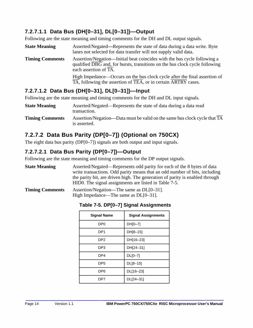
7.2.7.1.1 Data Bus (DH[0–31], DL[0–31])—OutputFollowing are the state meaning and timing comments for the DH and DL output signals.
State Meaning Asserted/Negated—Represents the state of data during a data write. Byte lanes not selected for data transfer will not supply valid data.
Timing Comments Assertion/Negation—Initial beat coincides with the bus cycle following a qualified DBG and, for bursts, transitions on the bus clock cycle following each assertion of TA.
High Impedance—Occurs on the bus clock cycle after the final assertion of TA, following the assertion of TEA, or in certain ARTRY cases.
7.2.7.1.2 Data Bus (DH[0–31], DL[0–31])—InputFollowing are the state meaning and timing comments for the DH and DL input signals.
State Meaning Asserted/Negated—Represents the state of data during a data read transaction.
Timing Comments Assertion/Negation—Data must be valid on the same bus clock cycle that TA is asserted.
7.2.7.2 Data Bus Parity (DP[0–7]) (Optional on 750CX)The eight data bus parity (DP[0–7]) signals are both output and input signals.
7.2.7.2.1 Data Bus Parity (DP[0–7])—OutputFollowing are the state meaning and timing comments for the DP output signals.
State Meaning Asserted/Negated—Represents odd parity for each of the 8 bytes of data write transactions. Odd parity means that an odd number of bits, including the parity bit, are driven high. The generation of parity is enabled through HID0. The signal assignments are listed in Table 7-5.
Timing Comments Assertion/Negation—The same as DL[0–31].High Impedance—The same as DL[0–31].
Table 7-5. DP[0–7] Signal Assignments
Signal Name Signal Assignments
DP0 DH[0–7]
DP1 DH[8–15]
DP2 DH[16–23]
DP3 DH[24–31]
DP4 DL[0–7]
DP5 DL[8–15]
DP6 DL[16–23]
DP7 DL[24–31]
Page 14 Version 1.1 IBM PowerPC 750CX/750CXe RISC Microprocessor User’s Manual

7.2.7.2.2 Data Bus Parity (DP[0–7])—InputFollowing are the state meaning and timing comments for the DP input signals.
State Meaning Asserted/Negated—Represents odd parity for each byte of read data. Parity is checked on all data byte lanes, regardless of the size of the transfer. Detected even parity causes a checkstop if data parity errors are enabled in the HID0 register.
Timing Comments Assertion/Negation—The same as DL[0–31].
7.2.8 Data Transfer Termination SignalsData termination signals are required after each data beat in a data transfer. Note that in a single-beattransaction, the data termination signals also indicate the end of the tenure, while in burst accesses,the data termination signals apply to individual beats and indicate the end of the tenure only after thefinal data beat.
For a detailed description of how these signals interact, see Chapter 8.
7.2.8.1 Transfer Acknowledge (TA)—InputFollowing are the state meaning and timing comments for the TA signal.
State Meaning Asserted— Indicates that a single-beat data transfer completed successfully or that a data beat in a burst transfer completed successfully. Note that TA must be asserted for each data beat in a burst transaction. For more information, see Chapter 8.
Negated—If the 750CX is the data bus master, then the 750CX must continue to drive the data for the current write or must wait to sample the data for reads until TA is asserted.
Timing Comments Assertion—Must not occur before AACK for the current transaction (if the address retry mechanism is to be used to prevent invalid data from being used by the processor); otherwise, assertion may occur at any time the 750CX while the 750CX is the data bus master. The system can withhold assertion of TA to indicate that the 750CX should insert wait states to extend the duration of the data beat.
Negation—Must occur after the bus clock cycle of the final (or only) data beat of the transfer. For a burst transfer, the system can assert TA for one bus clock cycle and then negate it to advance the burst transfer to the next beat and insert wait states during the next beat.
7.2.8.2 Data Retry (DRTRY)—Input (Optional on 750CX)Following are the state meaning and timing comments for the DRTRY signal.
State Meaning Asserted—Indicates that the 750CX must invalidate the data from the previous read operation.
Negated—Indicates that data presented with TA on the previous read operation is valid. Note that DRTRY is ignored for write transactions.
Timing Comments Assertion—Must occur during the bus clock cycle immediately after TA is asserted if a retry is required. The DRTRY signal may be held asserted for
Table of Contents 5/9/02 Page 15

multiple bus clock cycles. When DRTRY is negated, data must have been valid on the previous clock with TA asserted.
Negation—Must occur during the bus clock cycle after a valid data beat. This may occur several cycles effectively extending the data bus tenure.
Start-up—The DRTRY signal is sampled at the negation of HRESET; if DRTRY is asserted, no-DRTRY mode is selected. If DRTRY is negated at start-up, DRTRY is enabled.
7.2.8.3 Transfer Error Acknowledge (TEA)—InputFollowing are the state meaning and timing comments for the TEA signal.
State Meaning Asserted—Indicates that a bus error occurred. Causes a machine check exception (and possibly causes the processor to enter checkstop state if machine check enable bit is cleared (MSR[ME] = 0)). For more information, see Section 4.5.2.2, “Checkstop State (MSR[ME] = 0)" on Page 4-18. Assertion terminates the current transaction; that is, assertion of TA is ignored. The assertion of TEA causes data bus tenure to be dropped. However, data entering the GPR or the cache are not invalidated. (Note that the term ‘exception’ is also referred to as ‘interrupt’ in the architecture specification.)
Negated—Indicates that no bus error was detected.
Timing Comments Assertion—May be asserted while the 750CX is the data bus master, and the cycle after TA during a read operation. TEA should be asserted for one cycle only.
Negation—TEA must be negated no later than the end of the data bus tenure.
7.2.9 System Status SignalsMost system status signals are input signals that indicate when exceptions are received, whencheckstop conditions have occurred, and when the 750CX must be reset.
7.2.9.1 Interrupt (INT)— InputFollowing are the state meaning and timing comments for the INT signal.
State Meaning Asserted— The 750CX initiates an interrupt if MSR[EE] is set; otherwise, the 750CX ignores the interrupt. To guarantee that the 750CX will take the external interrupt, INT must be held active until the 750CX takes the interrupt; otherwise, whether the 750CX takes an external interrupt depends on whether the MSR[EE] bit was set while the INT signal was held active.
Negated—Indicates that normal operation should proceed. See Chapter 8.
Timing Comments Assertion—May occur at any time and may be asserted asynchronously to the input clocks. The INT input is level-sensitive.Negation—Should not occur until interrupt is taken.
Page 16 Version 1.1 IBM PowerPC 750CX/750CXe RISC Microprocessor User’s Manual

7.2.9.2 Machine Check Interrupt (MCP)—InputFollowing are the state meaning and timing comments for the MCP signal.
State Meaning Asserted—The 750CX initiates a machine check interrupt operation if MSR[ME] and HID0[EMCP] are set; if MSR[ME] is cleared and HID0[EMCP] is set, the 750CX must terminate operation by internally gating off all clocks, and releasing all outputs to the high-impedance state. If HID0[EMCP] is cleared, the 750CX ignores the interrupt condition. The MCP signal must be held asserted for two bus clock cycles.
Negated—Indicates that normal operation should proceed. See Section 8.8.1, “External Interrupts" on Page 8-37.
Timing Comments Assertion—May occur at any time and may be asserted asynchronously to the input clocks. The MCP input is negative edge-sensitive.
Negation—May be negated two bus cycles after assertion.
7.2.9.3 Checkstop Input (CKSTP_IN)—Input Following are the state meaning and timing comments for the CKSTP_IN signal.
State Meaning Asserted—Indicates that the 750CX must terminate operation by internally gating off all clocks, and release all outputs to the high-impedance state. Once CKSTP_IN has been asserted it must remain asserted until the system has been reset.
Negated—Indicates that normal operation should proceed. See Chapter 8.
Timing Comments Assertion—May occur at any time and may be asserted asynchronously to the input clocks.
Negation—May occur any time after the system reset.
7.2.9.4 Checkstop Output (CKSTP_OUT)—OutputNote that the CKSTP_OUT signal is an open-drain type output, and requires an external pull-upresistor (for example, 10 k¾ to Vdd) to assure proper de-assertion of the CKSTP_OUT signal.Following are the state meaning and timing comments for the CKSTP_OUT signal.
State Meaning Asserted—Indicates that a checkstop condition has been detected and the processor has ceased operation.
Negated—Indicates that the processor is operating normally.See Chapter 8.
Timing Comments Assertion—May occur at any time and may be asserted asynchronously to input clocks.
Negation—Is negated upon assertion of HRESET.
Table of Contents 5/9/02 Page 17

7.2.9.5 Reset SignalsThere are two reset signals on the 750CX—hard reset (HRESET) and soft reset (SRESET).Descriptions of the reset signals are as follows:
7.2.9.5.1 Hard Reset (HRESET)—InputThe hard reset (HRESET) signal must be used at power-on in conjunction with the TRST signal toproperly reset the processor. Following are the state meaning and timing comments for the HRESETsignal.
State Meaning Asserted—Initiates a complete hard reset operation when this input transitions from asserted to negated. Causes a reset exception as described in Section 4.5.1, “System Reset Exception (0x00100)" on Page 4-13 Output drivers are released to high impedance within five clocks after the assertion of HRESET.
Negated—Indicates that normal operation should proceed. See Section 8.8.3, “Reset Inputs" on Page 8-38.
Timing Comments Assertion—May occur at any time and may be asserted asynchronously to the 750CX input clock; must be held asserted for a minimum of 255 clock cycles after the PLL lock time has been met. Refer to the 750CX hardware specifications for further timing comments.
Negation—May occur any time after the minimum reset pulse width has been met.
This input has additional functionality in certain test modes.
7.2.9.5.2 Soft Reset (SRESET)—InputFollowing are the state meaning and timing comments for the SRESET signal.
State Meaning Asserted— Initiates processing for a reset exception as described in Section 4.5.1, “System Reset Exception (0x00100)" on Page 4-13.
Negated—Indicates that normal operation should proceed. See Section 8.8.3, “Reset Inputs" on Page 8-38.
Timing Comments Assertion—May occur at any time and may be asserted asynchronously to the 750CX input clock. The SRESET input is negative edge-sensitive.
Negation—May be negated two bus cycles after assertion.
This input has additional functionality in certain test modes.
Page 18 Version 1.1 IBM PowerPC 750CX/750CXe RISC Microprocessor User’s Manual
7.2.9.6 Processor Status SignalsProcessor status signals indicate the state of the processor. This includes the machine quiesce controlsignals, and TLBISYNC signal. The latter is optional on the 750CX.
7.2.9.6.1 Quiescent Request (QREQ)—OutputFollowing are the state meaning and timing comments for QREQ.
State Meaning Asserted—Indicates that the 750CX is requesting all bus activity normally required to be snooped to terminate or to pause so 750CX may enter a quiescent (low power) state. When the 750CX has entered a quiescent state, it no longer snoops bus activity.
Negated—Indicates that the 750CX is not making a request to enter the quiescent state.
Timing Comments Assertion/Negation—May occur on any cycle. QREQ will remain asserted for the duration of the quiescent state.
7.2.9.6.2 Quiescent Acknowledge (QACK)—InputFollowing are the state meaning and timing comments for the QACK signal.
State Meaning Asserted—Indicates that all bus activity that requires snooping has terminated or paused, and that the 750CX may enter the quiescent (or low power) state.
Negated—Indicates that the 750CX may not enter a quiescent state, and must continue snooping the bus.
Timing Comments Assertion/Negation—May occur on any cycle following the assertion of QREQ, and must be held asserted for at least one bus clock cycle.
Start-Up—QACK is sampled at the negation of HRESET to select 32-bit bus mode; if QACK is de-asserted at start-up, 32-bit bus mode is selected.
7.2.9.6.3 TLBI Sync (TLBISYNC)—Input (Optional on 750CX)The TLBI Sync (TLBISYNC) signal is an input-only signal. Following are the state meaning andtiming comments for the TLBISYNC signal.
State Meaning Asserted—Indicates that instruction execution stops after execution of a tlbsync instruction.
Negated—Indicates that the instruction execution may continue or resume after the completion of a tlbsync instruction.
Timing Comments Assertion/Negation—May occur on any cycle. The TLBISYNC signal must be held negated during HRESET.
Start-Up—TLBISYNC is sampled at the negation of HRESET to select 32-bit data bus mode; if TLBISYNC is negated at start-up, 32-bit mode is disabled, and the default 64-bit mode is selected.
Timing Comments Assertion/Negation—Refer to the hardware specifications for timing comments.
Table of Contents 5/9/02 Page 19

7.2.10 IEEE 1149.1a-1993 Interface DescriptionThe 750CX has five dedicated JTAG signals which are described in Table 7-6. The test data input(TDI) and test data output (TDO) scan ports are used to scan instructions as well as data into thevarious scan registers for JTAG operations. The scan operation is controlled by the
test access port (TAP) controller which in turn is controlled by the test mode select (TMS) inputsequence. The scan data is latched in at the rising edge of test clock (TCK).
Test reset (TRST) is a JTAG optional signal which is used to reset the TAP controller asynchronously.The TRST signal assures that the JTAG logic does not interfere with the normal operation of the chip,and must be asserted and deasserted coincident with the assertion of the HRESET signal.
7.2.11 Clock SignalsThe 750CX clock signal inputs determine the system clock frequency and provide a flexible clockingscheme that allows the processor to operate at an integer multiple of the system clock frequency.
Refer to the 750CX hardware specifications for exact timing relationships of the clock signals.
7.2.11.1 System Clock (SYSCLK)—InputThe 750CX requires a single system clock (SYSCLK) input. This input sets the frequency ofoperation for the bus interface. Internally, the 750CX uses a phase-locked loop (PLL) circuit togenerate a master clock for all of the CPU circuitry (including the bus interface circuitry) which isphase-locked to the SYSCLK input. The master clock may be set to an integer or half-integer multiple(2:1, 3:1, 3.5:1, 4:1, 4.5:1, 5:1, 5.5:1, 6:1, 6.5:1, 7:1, 7.5:1, 8:1 or 10:1) of the SYSCLK frequencyallowing the CPU core to operate at an equal or greater frequency than the bus interface.
State Meaning Asserted/Negated—The SYSCLK input is the primary clock input for the 750CX, and represents the bus clock frequency for the 750CX bus operation. Internally, the 750CX may be operating at an integer or half-integer multiple of the bus clock frequency.
Timing Comments Duty cycle—Refer to the 750CX hardware specifications for timing comments. Note: SYSCLK is used as the frequency reference for the internal PLL clock generator, and must not be suspended or varied during normal operation to ensure proper PLL operation.
Table 7-6. IEEE Interface Pin Descriptions
Signal Name Input/OutputWeak Pullup
ProvidedIEEE 1149.1a Function
TDI Input Yes Serial scan input signal
TDO Output No Serial scan output signal
TMS Input Yes TAP controller mode signal
TCK Input Yes Scan clock
TRST Input Yes TAP controller reset
Page 20 Version 1.1 IBM PowerPC 750CX/750CXe RISC Microprocessor User’s Manual

7.2.11.2 Clock Out (CLK_OUT)—Output (N/A on the 750CX)The clock out (CLK_OUT) signal is an output signal (output-only). Following are the state meaningand timing comments for the CLK_OUT signal.
State Meaning Asserted/Negated—Provides PLL clock output for PLL testing and monitoring. The configuration of the HID0[SBCLK] and HID0[ECLK] bits determines whether the CLK_OUT signal clocks at either the processor clock frequency, the bus clock frequency, or half of the bus clock frequency. See Table 2-6 on Page 2-13 for HID0 register configuration of the CLK_OUT signal. The CLK_OUT signal defaults to a high-impedance state following the assertion of HRESET. The CLK_OUT signal is provided for testing only.
Timing Comments Assertion/Negation—Refer to the 750CX hardware specifications for timing comments.
7.2.11.3 PLL Configuration (PLL_CFG[0–3])—InputThe PLL (phase-locked loop) is configured by the PLL_CFG[0–3] signals. For a given SYSCLK(bus) frequency, the PLL configuration signals set the internal CPU frequency of operation. Refer tothe 750CX hardware specifications for PLL configuration.
Following are the state meaning and timing comments for the PLL_CFG[0–3] signals.
State Meaning Asserted/Negated— Configures the operation of the PLL and the internal processor clock frequency. Settings are based on the desired bus and internal frequency of operation.
Timing Comments Assertion/Negation—Must remain stable during operation; should only be changed during the assertion of HRESET or during sleep mode. These bits may be read through the PC[0–3] bits in the HID1 register.
7.2.12 Power and Ground SignalsThe 750CX provides the following connections for power and ground:
• VDD—The VDD signals provide the supply voltage connection for the processor core.
• OVDD—The OVDD signals provide the supply voltage connection for the system interface drivers.
• AVDD—The AVDD power signal provides power to the clock generation phase-locked loop. See the 750CX hardware specifications for information on how to use this signal.
• GND and OGND—The GND and OGND signals provide the connection for grounding the 750CX. On the 750CX, there is no electrical distinction between the GND and OGND signals.
Table of Contents 5/9/02 Page 21

Page 22 Version 1.1 IBM PowerPC 750CX/750CXe RISC Microprocessor User’s Manual

Chapter 8 Bus Interface OperationThis chapter describes the 750CX microprocessor bus interface and its operation. It shows how the750CX signals, defined in Chapter 7, "Signal Descriptions" interact to perform address and datatransfers.
The bus interface buffers bus requests from the instruction and data caches, and executes the requestsper the 60x bus protocol. It includes address register queues, prioritizing logic, and bus control logic.It captures snoop addresses for snooping in the cache and in the address register queues. It also snoopsfor reservations and holds the touch load address for the cache. All data storage for the addressregister buffers (load and store data buffers) are located in the cache section. The data buffers areconsidered temporary storage for the cache and not part of the bus interface.
The general functions and features of the bus interface are as follows:• Seven address register buffers that include the following:
— Instruction cache load address buffer— Data cache load address buffer — Two data cache castout/store address buffers — Data cache snoop copy-back address buffer (associated data block buffer located in cache)— Reservation address buffer for snoop monitoring
• Pipeline collision detection for data cache buffers• Reservation address snooping for lwarx/stwcx. instructions• One-level address pipelining• Load ahead of store capability
A conceptual block diagram of the bus interface is shown in Figure 8-1. The address register queuesin the figure hold transaction requests that the bus interface may issue on the bus independently of theother requests. The bus interface may have up to two transactions operating on the bus at any giventime through the use of address pipelining.
Table of Contents 5/9/02 Page 1

Figure 8-1. Bus Interface Address Buffers
8.1 Bus Interface Overview The bus interface prioritizes requests for bus operations from the instruction and data caches, andperforms bus operations in accordance with the protocol described in the PowerPC MicroprocessorFamily: The Bus Interface for 32-Bit Microprocessors. It includes address register queues,prioritization logic, and bus control unit. The bus interface latches snoop addresses for snooping inthe data cache and in the address register queues, and for reservations controlled by the Load Wordand Reserve Indexed (lwarx) and Store Word Conditional Indexed (stwcx.) instructions, andmaintains the touch load address for the cache. The interface allows one level of pipelining; that is,with certain restrictions discussed later, there can be two outstanding transactions at any given time.Accesses are prioritized with load operations preceding store operations.
Instructions are automatically fetched from the memory system into the instruction unit (a maximumof four per cycle) where they are dispatched to the execution units at a peak rate of two instructionsper clock. Conversely, load and store instructions explicitly specify the movement of operands to andfrom the integer and floating-point register files and the memory system.
When the 750CX encounters an instruction or data access, it calculates the logical address (effectiveaddress in the architecture specification) and uses the low-order address bits to check for a hit in theL1, 32-Kbyte instruction and data caches.
During cache lookup, the instruction and data memory management units (MMUs) use thehigher-order address bits to calculate the virtual address from which they calculate the physicaladdress (real address in the architecture specification). The physical address bits are then comparedwith the corresponding cache tag bits to determine if a cache hit occurred in the L1 instruction or datacache. If the access misses in the corresponding cache, the physical address is used to access the L2
Snoop
Control Addr Addr Data
System Bus
I-Cache
D-Cache
D-CacheCST/ST Addr 1
D-CacheSNP Addr
D-CacheCST/ST Addr 0
I-CacheLD Addr
D-CacheLD Addr
Data
BIUControl
Data
Page 2 Version 1.1 IBM PowerPC 750CX/750CXe RISC Microprocessor User’s Manual

cache tags (if the L2 cache is enabled). If no match is found in the L2 cache tags, the physical addressis used to access system memory.
In addition to the loads, stores, and instruction fetches, the 750CX performs hardware table searchoperations following TLB misses, L2 cache cast-out operations when least-recently used cache linesare written to memory after a cache miss, and cache-line snoop push-out operations when a modifiedcache line experiences a snoop hit from another bus master.
Figure 8-2 on page 8-5 shows the address path from the execution units and instruction fetcher,through the translation logic to the caches and bus interface logic.
The 750CX uses separate address and data buses and a variety of control and status signals forperforming reads and writes. The address bus is 32 bits wide and the data bus is 64 bits wide. Theinterface is synchronous—all the 750CX inputs are sampled at and all outputs are driven from therising edge of the bus clock. The processor runs at a multiple of the bus-clock speed.
8.1.1 Operation of the Instruction and Data L1 Caches The 750CX provides independent instruction and data L1 caches. Each cache is aphysically-addressed, 32-Kbyte cache with eight-way set associativity. Both caches consist of 128sets of eight cache lines, with eight words in each cache line.
Because the data cache on the 750CX is an on-chip, write-back primary cache, the predominant typeof transaction for most applications is burst-read memory operations, followed by burst-writememory operations and single-beat (noncacheable or write-through) memory read and writeoperations. Additionally, there can be address-only operations, variants of the burst and single-beatoperations (global memory operations that are snooped, and atomic memory operations, forexample), and address retry activity (for example, when a snooped read access hits a modified line inthe cache).
Since the 750CX’s data cache tags are single ported, simultaneous load or store, and snoop accessescause resource contention. Snoop accesses have the highest priority and are given first access to thetags, unless the snoop access coincides with a tag write, in which case the snoop is retried and mustre-arbitrate for access to the cache. Loads or stores that are deferred due to snoop accesses areperformed on the clock cycle following the snoop.
The 750CX supports a three-state coherency protocol that supports the modified, exclusive, andinvalid (MEI) cache states. The protocol is a subset of the MESI (modified/exclusive/shared/invalid)four-state protocol and operates coherently in systems that contain four-state caches.
With the exception of the dcbz instruction (and the dcbi, dcbst, and dcbf instructions, if HID0[ABE]is enabled), the 750CX does not broadcast cache control instructions. The cache control instructionsare intended for the management of the local cache but not for other caches in the system.
Instruction cache lines in the 750CX are loaded in four beats of 64 bits each. The burst load isperformed as critical double word first. The critical double word is simultaneously written to thecache and forwarded to the instruction pre-fetch unit, thus minimizing stalls due to load delays. Ifsubsequent loads follow in sequential order, the instructions will be forwarded to the requesting unitas the cache block is written.
Table of Contents 5/9/02 Page 3

Data cache lines in the 750CX are loaded into the cache in one cycle for 256 bits. For cache line loaddue to the cache miss of a load instruction, the critical double word is simultaneously written to the256 bit line fill buffer and forwarded to the requesting load/store unit. If subsequent loads follow insequential order, the data will be forwarded to the load/store unit as the cache block is written into thecache.
Cache lines are selected for replacement based on a pseudo least-recently-used (PLRU) algorithm.Each time a cache line is accessed, it is tagged as the most-recently-used line of the set. When a missoccurs, and all eight lines in the set are marked as valid, the least recently used line is replaced withthe new data. When data to be replaced is in the modified state, the modified data is written into awrite-back buffer while the missed data is being read from memory. When the load completes, the750CX then pushes the replaced line from the write-back buffer to the L2 cache (if enabled), or tomain memory in a burst write operation.
Page 4 Version 1.1 IBM PowerPC 750CX/750CXe RISC Microprocessor User’s Manual

Preliminary
Fig
ure
8-2.
Po
wer
PC
750
CX
Mic
rop
roce
sso
r B
lock
Dia
gra
m
Add
ition
al F
eatu
res
• T
ime
Bas
e C
ount
er/D
ec-
rem
ente
r
• C
lock
Mul
tiplie
r
• JT
AG
/CO
P In
terf
ace
+
+
Fetc
her
Bran
ch P
roce
ssin
g
BTIC
64 E
ntry
+ x
÷F
PS
CR
CR
FPSC
R
CTR LR
BHT
Data
MM
U
Inst
ruct
ion
MM
U
PAEA
+ x
÷
Inst
ruct
ion
Unit
Unit
Inst
ruct
ion
Que
ue(6
Wor
d)
2 In
stru
ctio
ns
Res
erva
tion
Stat
ion
Res
erva
tion
Stat
ion
Res
erva
tion
Stat
ion
Inte
ger U
nit 1
Syst
em R
egis
ter
Unit
Dis
patc
h U
nit
64-B
it(2
Inst
ruct
ions
)
SRs
ITLB
(Sha
dow
)IB
ATAr
ray
32-K
byte
I Cac
heTa
gs
128-
Bit
(4 In
stru
ctio
ns)
32-B
it
Floa
ting-
Poin
tUn
itR
enam
e Bu
ffers
(6)
FPR
File
32-B
it64
-Bit
64-B
it
Res
erva
tion
Stat
ion
(2 E
ntry
)
Load
/Sto
re U
nit
(EA
Cal
cula
tion)
Stor
e Q
ueue
GPR
File
Ren
ame
Buffe
rs(6
)
32-B
it
SRs
(Orig
inal
)
DTL
B
DBA
TAr
ray
64-B
itCo
mpl
etio
n Un
it
Reo
rder
Buf
fer
(6 E
ntry
)
60x
Bus
Inte
rface
Uni
tIn
stru
ctio
n Fe
tch
Que
ue
L1 C
asto
ut Q
ueue
Dat
a Lo
ad Q
ueue
L2 C
ache
32-B
it Ad
dres
s Bu
s64
-Bit
Dat
a Bu
s
Inte
ger U
nit 2
L2C
R
256K
byte
SR
AM
Tags
32-K
byte
D C
ache
Rese
rvat
ion
Stat
ion
L2 T
ag
(2 E
ntry
)
Table of Cont
ents 5/9/02 Page 5
8.1.2 Operation of the Bus Interface Memory accesses can occur in single-beat (1, 2, 3, 4, and 8 bytes) and four-beat (32 bytes) burst datatransfers. The address and data buses are independent for memory accesses to support pipelining andsplit transactions. The 750CX can pipeline as many as two transactions and has limited support forout-of-order split-bus transactions.
Access to the bus interface is granted through an external arbitration mechanism that allows devicesto compete for bus mastership. This arbitration mechanism is flexible, allowing the 750CX to beintegrated into systems that implement various fairness and bus-parking procedures to avoidarbitration overhead. Typically, memory accesses are weakly ordered to maximize the efficiency ofthe bus without sacrificing coherency of the data. The 750CX allows load operations to bypass storeoperations (except when a dependency exists). In addition, the 750CX can be configured to reorderhigh-priority store operations ahead of lower-priority store operations. Because the processor candynamically optimize run-time ordering of load/store traffic, overall performance is improved.
NOTE: The synchronize (sync) and enforce in-order execution of IO (eieio) instructions can be used to enforce strong ordering.
The following sections describe how the 750CX interface operates, providing detailed timingdiagrams that illustrate how the signals interact. A collection of more general timing diagrams areincluded as examples of typical bus operations.
Figure 8-3 on page 8-7 is a legend of the conventions used in the timing diagrams.
This is a synchronous interface—all the 750CX input signals are sampled and output signals aredriven on the rising edge of the bus clock cycle (see the 750CX Datasheet for exact timinginformation).
8.1.3 Direct-Store AccessesThe 750CX does not support the extended transfer protocol for accesses to the direct-store storagespace. The transfer protocol used for any given access is selected by the T bit in the MMU segmentregisters; if the T bit is set, the memory access is a direct-store access. An attempt to accessinstructions or data in a direct-store segment will result in the 750CX taking an ISI or DSI exception.
Page 6 Version 1.1 IBM PowerPC 750CX/750CXe RISC Microprocessor User’s Manual

Figure 8-3. Timing Diagram Legend
8.2 Memory Access Protocol Memory accesses are divided into address and data tenures. Each tenure has three phases—busarbitration, transfer, and termination. The 750CX also supports address-only transactions. Note thataddress and data tenures can overlap, as shown in Figure 8-4 on page 8-8.
Figure 8-4 shows that the address and data tenures are distinct from one another and that both consistof three phases—arbitration, transfer, and termination. Address and data tenures are independent(indicated in Figure 8-4 by the fact that the data tenure begins before the address tenure ends), whichallows split-bus transactions to be implemented at the system level in multiprocessor systems.
Figure 8-4 shows a data transfer that consists of a single-beat transfer of as many as 64 bits. Four-beatburst transfers of 32-byte cache lines require data transfer termination signals for each beat of data.
750CX input (while 750CX is a bus master)
750CX output (while 750CX is a bus master)
750CX output (grouped: here, address plus attributes)
750CX internal signal (inaccessible to the user, but usedin diagrams to clarify operations)
Compelling dependency—event will occur on thenext clock cycle
Prerequisite dependency—event will occur on anundetermined subsequent clock cycle
750CX three-state output or input
750CX nonsampled input
Signal with sample point
A sampled condition (dot on high or low state) with multiple dependencies
Timing for a signal had it been asserted (it is notactually asserted)
Bar over signal name indicates active low
ap0
BR
ADDR+
qual BG
Table of Contents
5/9/02 Page 7
Figure 8-4. Overlapping Tenures on the 750CX Bus for a Single-Beat Transfer
The basic functions of the address and data tenures are as follows.• Address tenure
— Arbitration: During arbitration, address bus arbitration signals are used to gain mastership of the address bus.
— Transfer: After the 750CX is the address bus master, it transfers the address on the address bus. The address signals and the transfer attribute signals control the address transfer. The address parity and address parity error signals ensure the integrity of the address transfer. (Parity is optional on the 750CX)
— Termination: After the address transfer, the system signals that the address tenure is complete or that it must be repeated.
• Data tenure— Arbitration: To begin the data tenure, the 750CX arbitrates for mastership of the data bus.— Transfer: After the 750CX is the data bus master, it samples the data bus for read
operations or drives the data bus for write operations. The data parity and data parity error signals ensure the integrity of the data transfer. (Parity is optional on the 750CX)
— Termination: Data termination signals are required after each data beat in a data transfer. Note that in a single-beat transaction, the data termination signals also indicate the end of the tenure, while in burst accesses, the data termination signals apply to individual beats and indicate the end of the tenure only after the final data beat.
The 750CX generates an address-only bus transfer during the execution of the dcbz instruction (andfor the dcbi, dcbf, dcbst, sync, and eieio instructions, if HID0[ABE] is enabled), which uses only theaddress bus with no data transfer involved. Additionally, the 750CX’s retry capability provides anefficient snooping protocol for systems with multiple memory systems (including caches) that mustremain coherent.
ARBITRATION TRANSFER TERMINATION
ADDRESS TENURE
ARBITRATION SINGLE-BEAT TRANSFER TERMINATION
DATA TENURE
INDEPENDENT ADDRESS AND DATA
Page 8
Version 1.1 IBM P owerPC 750CX/750CXe RIS C Microprocessor User’s Manual
8.2.1 Arbitration Signals Arbitration for both address and data bus mastership is performed by a central, external arbiter and,minimally, by the arbitration signals shown in Section 7.2.1 on Page 7-3. Most arbiterimplementations require additional signals to coordinate bus master/slave/snooping activities.
NOTE: Address bus busy (ABB) and data bus busy (DBB) signals are not supported on the 750CX. The 750CX uses internally generated signals, iABB and iDBB to determine the status of the bus transactions. The 750CX does not support the DRTRY signal pin which is internally configured as a pull-up. All the references to the DRTRY signal shall be considered as a permanently negated signal.
The following list describes the address arbitration signals:
• BR (bus request)—Assertion indicates that the 750CX is requesting mastership of the address bus.
• BG (bus grant)—Assertion indicates that the 750CX may, with the proper qualification, assume mastership of the address bus. A qualified bus grant occurs when BG is asserted and when iABB and ARTRY are negated.If the 750CX is parked, BR need not be asserted for the qualified bus grant.
The following list describes the data arbitration signals:• DBG (data bus grant)—Indicates that the 750CX may, with the proper qualification, assume
mastership of the data bus. A qualified data bus grant occurs when DBG is asserted while DRTRY, iDBB and ARTRY are negated.The ARTRY signal is driven from the bus and is only for the address bus tenure associated with the current data bus tenure (that is, not from another address tenure).The 750CX always assumes data bus mastership if it needs the data bus and is given a qualified data bus grant.For more detailed information on the arbitration signals, refer to Section 7.2.1 on Page 7-3 and Section 7.2.6 on Page 7-12.
8.2.2 Address Pipelining and Split-Bus Transactions The 750CX protocol provides independent address and data bus capability to support pipelined andsplit-bus transaction system organizations. Address pipelining allows the address tenure of a new bustransaction to begin before the data tenure of the current transaction has finished. Split-bustransaction capability allows other bus activity to occur (either from the same master or from differentmasters) between the address and data tenures of a transaction.
While this capability does not inherently reduce memory latency, support for address pipelining andsplit-bus transactions can greatly improve effective bus/memory throughput. For this reason, thesetechniques are most effective in shared-memory multimaster implementations where bus bandwidthis an important measurement of system performance.
External arbitration is required in systems in which multiple devices must compete for the system bus.The design of the external arbiter affects pipelining by regulating address bus grant (BG), data busgrant (DBG), and address acknowledge (AACK) signals. For example, a one-level pipeline is enabledby asserting AACK to the current address bus master and granting mastership of the address bus to
Table of Contents 5/9/02 Page 9

the next requesting master before the current data bus tenure has completed. Two address tenures canoccur before the current data bus tenure completes.
The 750CX can pipeline its own transactions to a depth of one level (intraprocessor pipelining);however, the 750CX bus protocol does not constrain the maximum number of levels of pipeliningthat can occur on the bus between multiple masters (interprocessor pipelining). The external arbitermust control the pipeline depth and synchronization between masters and slaves.
In a pipelined implementation, data bus tenures are kept in strict order with respect to address tenures.However, external hardware can further decouple the address and data buses, allowing the datatenures to occur out of order with respect to the address tenures. This requires some form of systemtag to associate the out-of-order data transaction with the proper originating address transaction (notdefined for the 750CX interface). Individual bus requests and data bus grants from each processor canbe used by the system to implement tags to support interprocessor, out-of-order transactions.
NOTE: The 750CX drops out of pipeline mode between consecutive burst data reads and between consecutive burst instruction fetches. No other sequences of operations cause this effect. In this case, the address tenure of the second transaction will not begin until one to three bus clocks after the end of the data tenure of the first transaction.
8.3 Address Bus TenureThis section describes the three phases of the address tenure—address bus arbitration, addresstransfer, and address termination.
8.3.1 Address Bus Arbitration The 750CX replaces the ABB signal with an internal signal, iABB, which is asserted on TS and isnegated the cycle after AACK.
When the 750CX needs access to the external bus and it is not parked (BG is negated), it asserts busrequest (BR) until it is granted mastership of the bus and the bus is available (see Figure 8-5 on page8-11). The external arbiter must grant master-elect status to the potential master by asserting the busgrant (BG) signal. The 750CX determines that the address bus is not busy by monitoring the TS andthe AACK input signals. The 750CX determines that the bus is available when the address bus is notbusy, BG is asserted and the address retry (ARTRY) input is negated. This is referred to as a qualifiedbus grant and the 750CX can assume address bus mastership.
Page 10 Version 1.1 IBM PowerPC 750CX/750CXe RISC Microprocessor User’s Manual

Figure 8-5. Address Bus Arbitration
External arbiters must allow only one device at a time to be the address bus master. Forimplementations in which no other device can be a master, BG can be grounded (always asserted) tocontinually grant mastership of the address bus to 750CX.
If the 750CX asserts BR before the external arbiter asserts BG, 750CX is considered to be unparked,as shown in Figure 8-5. Figure 8-6 on page 8-12 shows the parked case, where a qualified bus grantexists on the clock edge following a need_bus condition. Notice that the bus clock cycle required forarbitration is eliminated if the 750CX is parked, reducing overall memory latency for a transaction.The 750CX always negates iABB for at least one bus clock cycle after AACK is asserted, even if itis parked and has another transaction pending.
Typically, bus parking is provided to the device that was the most recent bus master; however, systemdesigners may choose other schemes such as providing unrequested bus grants in situations where itis easy to correctly predict the next device requesting bus mastership.
-101
need_bus
BR
bg
artry
qual BG
iABB
Logical Bus Clock
Table of Contents
5/9/02 Page 11
Figure 8-6. Address Bus Arbitration Showing Bus Parking
When the 750CX receives a qualified bus grant, it assumes address bus mastership by negating theBR output signal. Meanwhile, the 750CX drives the address for the requested access onto the addressbus and asserts TS to indicate the start of a new transaction.
When designing external bus arbitration logic, note that the 750CX may assert BR without using thebus after it receives the qualified bus grant. For example, in a system using bus snooping, if the750CX asserts BR to perform a replacement copy-back operation, another device can invalidate thatline before the 750CX is granted mastership of the bus. In these instances, the 750CX asserts BR forat least one clock cycle.
System designers should note that the 750CX does not support the ABB signal. The memorycontroller must monitor the TS and AACK input signals to determine the status of the address bus.The 750CX allows this operation by using an internal version of ABB to determine if a qualified busgrant state exists.
The 750CX will not qualify a bus grant during the cycle that TS is asserted on the bus by any master.Address bus arbitration requires that every assertion of TS be acknowledged by an assertion ofAACK while the processor is not in sleep mode.
-101
need_bus
BR
bg
artry
qual BG
iABB
Page 12 Version 1.1
IBM PowerPC 750CX/750CXe RISC Microprocessor User’s Manual
8.3.2 Address Transfer During the address transfer, the physical address and all attributes of the transaction are transferredfrom the bus master to the slave device(s). Snooping logic may monitor the transfer to enforce cachecoherency; see discussion about snooping in Section 8.3.3 on Page 8-18. The signals used in theaddress transfer include the following signal groups:
• Address transfer start signal: transfer start (TS) • Address transfer signals: address bus (A[0–31]), and address parity (AP[0–3]) (Parity is
optional on the 750CX)• Address transfer attribute signals: transfer type (TT[0–4]), transfer size (TSIZ[0–2]), transfer
burst (TBST), cache inhibit (CI), write-through (WT), and global (GBL).
Figure 8-7 shows that the timing for all of these signals, except TS, is identical. All of the addresstransfer and address transfer attribute signals are combined into the ADDR+ grouping in Figure 8-7.The TS signal indicates that the 750CX has begun an address transfer and that the address and transferattributes are valid (within the context of a synchronous bus).
In Figure 8-7, the address transfer occurs during bus clock cycles 1 and 2 (arbitration occurs in busclock cycle 0 and the address transfer is terminated in bus clock 3). In this diagram, the address bustermination input, AACK, is asserted to the 750CX on the bus clock following assertion of TS (asshown by the dependency line). This is the minimum duration of the address transfer for the 750CX;the duration can be extended by delaying the assertion of AACK for one or more bus clocks.
Figure 8-7. Address Bus Transfer
01234
qual BG
TS
iABB
ADDR+
aack
artry_in
Table of Contents
5/9/02 Page 13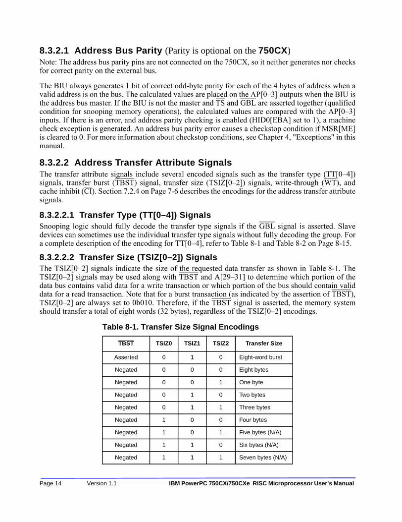
8.3.2.1 Address Bus Parity (Parity is optional on the 750CX)Note: The address bus parity pins are not connected on the 750CX, so it neither generates nor checksfor correct parity on the external bus.
The BIU always generates 1 bit of correct odd-byte parity for each of the 4 bytes of address when avalid address is on the bus. The calculated values are placed on the AP[0–3] outputs when the BIU isthe address bus master. If the BIU is not the master and TS and GBL are asserted together (qualifiedcondition for snooping memory operations), the calculated values are compared with the AP[0–3]inputs. If there is an error, and address parity checking is enabled (HID0[EBA] set to 1), a machinecheck exception is generated. An address bus parity error causes a checkstop condition if MSR[ME]is cleared to 0. For more information about checkstop conditions, see Chapter 4, "Exceptions" in thismanual.
8.3.2.2 Address Transfer Attribute SignalsThe transfer attribute signals include several encoded signals such as the transfer type (TT[0–4])signals, transfer burst (TBST) signal, transfer size (TSIZ[0–2]) signals, write-through (WT), andcache inhibit (CI). Section 7.2.4 on Page 7-6 describes the encodings for the address transfer attributesignals.
8.3.2.2.1 Transfer Type (TT[0–4]) SignalsSnooping logic should fully decode the transfer type signals if the GBL signal is asserted. Slavedevices can sometimes use the individual transfer type signals without fully decoding the group. Fora complete description of the encoding for TT[0–4], refer to Table 8-1 and Table 8-2 on Page 8-15.
8.3.2.2.2 Transfer Size (TSIZ[0–2]) SignalsThe TSIZ[0–2] signals indicate the size of the requested data transfer as shown in Table 8-1. TheTSIZ[0–2] signals may be used along with TBST and A[29–31] to determine which portion of thedata bus contains valid data for a write transaction or which portion of the bus should contain validdata for a read transaction. Note that for a burst transaction (as indicated by the assertion of TBST),TSIZ[0–2] are always set to 0b010. Therefore, if the TBST signal is asserted, the memory systemshould transfer a total of eight words (32 bytes), regardless of the TSIZ[0–2] encodings.
Table 8-1. Transfer Size Signal Encodings
TBST TSIZ0 TSIZ1 TSIZ2 Transfer Size
Asserted 0 1 0 Eight-word burst
Negated 0 0 0 Eight bytes
Negated 0 0 1 One byte
Negated 0 1 0 Two bytes
Negated 0 1 1 Three bytes
Negated 1 0 0 Four bytes
Negated 1 0 1 Five bytes (N/A)
Negated 1 1 0 Six bytes (N/A)
Negated 1 1 1 Seven bytes (N/A)
Page 14 Version 1.1 IBM PowerPC 750CX/750CXe RISC Microprocessor User’s Manual

The basic coherency size of the bus is defined to be 32 bytes (corresponding to one cache line). Datatransfers that cross an aligned, 32-byte boundary either must present a new address onto the bus atthat boundary (for coherency consideration) or must operate as noncoherent data with respect to the750CX. The 750CX never generates a bus transaction with a transfer size of 5 bytes, 6 bytes, or 7bytes.
8.3.2.2.3 Write-Through (WT) SignalThe 750CX provides the WT signal to indicate a write-through operation as determined by the WIMbit settings during address translation by the MMU. The WT signal is also asserted for burst writesdue to the execution of the dcbf and dcbst instructions, and snoop push operations. The WT signal isdeasserted for accesses caused by the execution of the ecowx instruction. During read operations the750CX uses the WT signal to indicate whether the transaction is an instruction fetch (WT set to 1),or a data read operation (WT cleared to 0).
8.3.2.2.4 Cache Inhibit (CI) SignalThe 750CX indicates the caching-inhibited status of a transaction (determined by the setting of theWIM bits by the MMU) through the use of the CI signal. The CI signal is asserted even if the L1caches are disabled or locked. This signal is also asserted for bus transactions caused by the executionof eciwx and ecowx instructions independent of the address translation.
8.3.2.3 Burst Ordering During Data TransfersDuring burst data transfer operations, 32 bytes of data (one cache line) are transferred to or from thecache in order. Burst write transfers are always performed zero double word first, but since burst readsare performed critical double word first, a burst read transfer may not start with the first double wordof the cache line, and the cache line fill may wrap around the end of the cache line.
Table 8-2 describes the data bus burst ordering.
Table 8-2. Burst Ordering
Data TransferFor Starting Address:
A[27–28] = 00 A[27–28] = 01 A[27–28] = 10 A[27–28] = 11
First data beat DW0 DW1 DW2 DW3
Second data beat DW1 DW2 DW3 DW0
Third data beat DW2 DW3 DW0 DW1
Fourth data beat DW3 DW0 DW1 DW2
Note: A[29–31] are always 0b000 for burst transfers by 750CX.
Table of Contents 5/9/02 Page 15

8.3.2.4 Effect of Alignment in Data TransfersTable 8-3 lists the aligned transfers that can occur on the 750CX bus. These are transfers in which thedata is aligned to an address that is an integral multiple of the size of the data. For example, Table 8-3shows that 1-byte data is always aligned; however, for a 4-byte word to be aligned, it must be orientedon an address that is a multiple of 4.
The 750CX supports misaligned memory operations, although their use may substantially degradeperformance. Misaligned memory transfers address memory that is not aligned to the size of the databeing transferred (such as, a word read of an odd byte address). Although most of these operationshit in the primary cache (or generate burst memory operations if they miss), the 750CX interfacesupports misaligned transfers within a word (32-bit aligned) boundary, as shown in Table 8-4 on Page8-17.
Table 8-3. Aligned Data Transfers
Transfer Size TSIZ0 TSIZ1 TSIZ2 A[29–31]Data Bus Byte Lane(s)
0 1 2 3 4 5 6 7
Byte 0 0 1 000 x — — — — — — —
0 0 1 001 — x — — — — — —
0 0 1 010 — — x — — — — —
0 0 1 011 — — — x — — — —
0 0 1 100 — — — — x — — —
0 0 1 101 — — — — — x — —
0 0 1 110 — — — — — — x —
0 0 1 111 — — — — — — — x
Half word 0 1 0 000 x x — — — — — —
0 1 0 010 — — x x — — — —
0 1 0 100 — — — — x x — —
0 1 0 110 — — — — — — x x
Word 1 0 0 000 x x x x — — — —
1 0 0 100 — — — — x x x x
Double word 0 0 0 000 x x x x x x x x
Note: The entries with an “x” indicate the byte portions of the requested operand which are read or written during a bus transaction.The entries with a “–” are not required and are ignored during read transactions, and they are driven with undefined data during all write transactions.
Page 16 Version 1.1 IBM PowerPC 750CX/750CXe RISC Microprocessor User’s Manual

NOTE: The 4-byte transfer in Table 8-4 is only one example of misalignment. As long as the attempted transfer does not cross a word boundary, 750CX can transfer the data on the misaligned address (for example, a half-word read from an odd byte-aligned address). An attempt to address data that crosses a word boundary requires two bus transfers to access the data.
Due to the performance degradations associated with misaligned memory operations, they are bestavoided. In addition to the double-word straddle boundary condition, the address translation logic cangenerate substantial exception overhead when the load/store multiple and load/store stringinstructions access misaligned data. It is strongly recommended that software attempt to align datawhere possible.
Table 8-4. Misaligned Data Transfers (Four-Byte Examples)
Transfer Size(Four Bytes)
TSIZ[0–2] A[29–31]Data Bus Byte Lanes
0 1 2 3 4 5 6 7
Aligned 1 0 0 0 0 0 A A A A — — — —
Misaligned—first access
second access
0 1 1 0 0 1 A A A — — — —
0 0 1 1 0 0 — — — — A — — —
Misaligned—first access
second access
0 1 0 0 1 0 — — A A — — — —
0 1 1 1 0 0 — — — — A A — —
Misaligned—first access
second access
0 0 1 0 1 1 — — — A — — — —
0 1 1 1 0 0 — — — — A A A —
Aligned 1 0 0 1 0 0 — — — — A A A A
Misaligned—first access
second access
0 1 1 1 0 1 — — — — — A A A
0 0 1 0 0 0 A — — — — — — —
Misaligned—first access
second access
0 1 0 1 1 0 — — — — — — A A
0 1 0 0 0 0 A A — — — — — —
Misaligned—first access
second access
0 0 1 1 1 1 — — — — — — — A
0 1 1 0 0 0 A A A — — — — —
Notes:
A: Byte lane used—: Byte lane not used
Table of Contents 5/9/02 Page 17

8.3.2.5 Alignment of External Control InstructionsThe size of the data transfer associated with the eciwx and ecowx instructions is always 4 bytes. Ifthe eciwx or ecowx instruction is misaligned and crosses any word boundary, the 750CX willgenerate an alignment exception.
8.3.3 Address Transfer TerminationThe address tenure of a bus operation is terminated when completed with the assertion of AACK, orretried with the assertion of ARTRY. The 750CX does not terminate the address transfer until theAACK (address acknowledge) input is asserted; therefore, the system can extend the address transferphase by delaying the assertion of AACK to the 750CX. The assertion of AACK can be as early asthe bus clock cycle following TS (see Figure 8-8 on page 8-19), which allows a minimum addresstenure of two bus cycles. As shown in Figure 8-8, these signals are asserted for one bus clock cycle,three-stated for half of the next bus clock cycle, driven high till the following bus cycle, and finallythree-stated. Note that AACK must be asserted for only one bus clock cycle.
The address transfer can be terminated with the requirement to retry if ARTRY is asserted anytimeduring the address tenure and through the cycle following AACK. The assertion causes the entiretransaction (address and data tenure) to be rerun. As a snooping device, the 750CX asserts ARTRYfor a snooped transaction that hits modified data in the data cache that must be written back tomemory, or if the snooped transaction could not be serviced. As a bus master, the 750CX responds toan assertion of ARTRY by aborting the bus transaction and re-requesting the bus. Note that afterrecognizing an assertion of ARTRY and aborting the transaction in progress, the 750CX is notguaranteed to run the same transaction the next time it is granted the bus due to internal reordering ofload and store operations.
If an address retry is required, the ARTRY response will be asserted by a bus snooping device as earlyas the second cycle after the assertion of TS. Once asserted, ARTRY must remain asserted throughthe cycle after the assertion of AACK. The assertion of ARTRY during the cycle after the assertionof AACK is referred to as a qualified ARTRY. An earlier assertion of ARTRY during the addresstenure is referred to as an early ARTRY.
As a bus master, the 750CX recognizes either an early or qualified ARTRY and prevents the datatenure associated with the retried address tenure. If the data tenure has already begun, the 750CXaborts and terminates the data tenure immediately even if the burst data has been received. If theassertion of ARTRY is received up to or on the bus cycle following the first (or only) assertion of TAfor the data tenure, the 750CX ignores the first data beat, and if it is a load operation, does not forwarddata internally to the cache and execution units. If ARTRY is asserted after the first (or only) assertionof TA, improper operation of the bus interface may result.
During the clock of a qualified ARTRY, the 750CX also determines if it should negate BR and ignoreBG on the following cycle. On the following cycle, only the snooping master that asserted ARTRYand needs to perform a snoop copy-back operation is allowed to assert BR. This guarantees thesnooping master an opportunity to request and be granted the bus before the just-retried master canrestart its transaction. Note that a nonclocked bus arbiter may detect the assertion of address busrequest by the bus master that asserted ARTRY, and return a qualified bus grant one cycle earlier thanshown in Figure 8-8.
Note that if the 750CX asserts ARTRY due to a snoop operation, and asserts BR in the bus cyclefollowing ARTRY in order to perform a snoop push to memory it may be several bus cycles later
Page 18 Version 1.1 IBM PowerPC 750CX/750CXe RISC Microprocessor User’s Manual

before the 750CX will be able to accept a BG. (The delay in responding to the assertion of BG onlyoccurs during snoop pushes from the L2 cache.) The bus arbiter should keep BG asserted until itdetects BR negated or TS asserted from the 750CX indicating that the snoop copy-back has begun.The system should ensure that no other address tenures occur until the current snoop push from the750CX is completed. Snoop push delays can also be avoided by operating the L2 cache inwrite-through mode so no snoop pushes are required by the L2 cache.
Figure 8-8. Snooped Address Cycle with ARTRY
8.4 Data Bus TenureThis section describes the data bus arbitration, transfer, and termination phases defined by the 750CXmemory access protocol. The phases of the data tenure are identical to those of the address tenure,underscoring the symmetry in the control of the two buses.
The 750CX does not support the DBB signal, typically found on a 60x PowerPC processor. Instead,the 750CX uses an internal signal, iDBB. The iDBB signal is asserted on the bus clock cyclefollowing a qualified DBG and is negated at least one bus clock cycle after the assertion of the finalTA. Also, the 750CX is configured to operate in no-DRTRY mode, so the state of the DRTRY signalas described in the following sections is ignored by the processor.(DRTRY is optional on the 750CX)
1234567
ts
addr
aack
ARTRY
BR
qualBG
iABB
8
Table of Conte
nts 5/9/02 Page 19
8.4.1 Data Bus ArbitrationData bus arbitration uses the data arbitration signal group—DBG and iDBB. Additionally, thecombination of TS and TT[0–4] provides information about the data bus request to external logic.
The TS signal is an implied data bus request from the 750CX. The arbiter must qualify TS with thetransfer type (TT) encodings to determine if the current address transfer is an address-only operation,which does not require a data bus transfer. If the data bus is needed, the arbiter grants data busmastership by asserting the DBG input to the 750CX. As with the address bus arbitration phase, the750CX must qualify the DBG input with a number of input signals before assuming bus mastership,as shown in Figure 8-9.
Figure 8-9. Data Bus Arbitration
A qualified data bus grant can be expressed as the following.QDBG = DBG asserted while DRTRY, iDBB and ARTRY (associated with the data bus operation) are negated.
When a data tenure overlaps with its associated address tenure, a qualified ARTRY assertioncoincident with a data bus grant signal does not result in data bus mastership Otherwise, the 750CXalways becomes the bus master on the bus clock cycle after recognition of a qualified data bus grant.Since the 750CX can pipeline transactions, there may be an outstanding data bus transaction when anew address transaction is retried. In this case, the 750CX becomes the data bus master to completethe outstanding transaction.
The 750CX does not support the DBB signal. The memory system must track the start and end of thedata tenure and control data tenure scheduling directly with DBG. The DBG signal is only asserted tothe next bus master the cycle before the cycle that the next bus master may actually begin its datatenure. The 750CX always requires one cycle after data tenure completion before recognizing aqualified data bus grant for another data tenure.
0123
TS
dbg
drtry
qual DBG
iDBB
Page 20 Version 1.1
IBM PowerPC 750CX/750CXe RISC Microprocessor User’s Manual
8.4.2 Data TransferThe data transfer signals include DH[0–31], DL[0–31], and DP[0–7]. For memory accesses, the DHand DL signals form a 64-bit data path for read and write operations.
The 750CX transfers data in either single- or four-beat burst transfers. Single-beat operations cantransfer from 1 to 8 bytes at a time and can be misaligned; see Section 8.3.2.4 on Page 8-16. Burstoperations always transfer eight words and are aligned on eight-word address boundaries. Bursttransfers can achieve significantly higher bus throughput than single-beat operations.
The type of transaction initiated by the 750CX depends on whether the code or data is cacheable and,for store operations whether the cache is in write-back or write-through mode, which softwarecontrols on either a page or block basis. Burst transfers support cacheable operations only; that is,memory structures must be marked as cacheable (and write-back for data store operations) in therespective page or block descriptor to take advantage of burst transfers.
The 750CX output TBST indicates to the system whether the current transaction is a single- orfour-beat transfer (except during eciwx/ecowx transactions, when it signals the state of EAR[28]). Aburst transfer has an assumed address order. For load or store operations that miss in the cache (andare marked as cacheable and, for stores, write-back in the MMU), the 750CX uses thedouble-word-aligned address associated with the critical code or data that initiated the transaction.This minimizes latency by allowing the critical code or data to be forwarded to the processor beforethe rest of the cache line is filled. For all other burst operations, however, the cache line is transferredbeginning with the eight-word-aligned data.
8.4.3 Data Transfer TerminationThree signals are used to terminate data bus transactions—TA, TEA (transfer error acknowledge),and ARTRY.
The TA signal indicates normal termination of data transactions. It must always be asserted on thebus cycle coincident with the data that it is qualifying. It may be withheld by the slave for any numberof clocks until valid data is ready to be supplied or accepted. Upon receiving a final (or only)termination condition, the 750CX always negates iDBB for one cycle.
The TEA signal is used to signal a nonrecoverable error during the data transaction. It may be assertedon any cycle during a data bus tenure. The assertion of TEA terminates the data tenure immediatelyeven if in the middle of a burst; however, it does not prevent incorrect data that has just beenacknowledged with TA from being written into the 750CX’s cache or GPRs. The assertion of TEAinitiates either a machine check exception or a checkstop condition based on the setting of theMSR[ME] bit.
An assertion of ARTRY causes the data tenure to be terminated immediately if the ARTRY is for theaddress tenure associated with the data tenure in operation. If ARTRY is connected for the 750CX,the earliest allowable assertion of TA to the 750CX is directly dependent on the earliest possibleassertion of ARTRY to the 750CX; see Section 8.3.3 on Page 8-18.
Table of Contents 5/9/02 Page 21

8.4.3.1 Normal Single-Beat TerminationNormal termination of a single-beat data read operation occurs when TA is asserted by a respondingslave. The TEA and DRTRY signals must remain negated during the transfer (see Figure 8-10).
Figure 8-10. Normal Single-Beat Read Termination
The DRTRY signal is not sampled during data writes, as shown in Figure 8-11.
Figure 8-11. Normal Single-Beat Write Termination
01234
TS
qual DBG
iDBB
data
ta
drtry
AACK
0123
TS
qual DBG
iDBB
data
ta
drtry
AACK
Page 22 Version 1.
1 IBM PowerPC 750CX/750CXe RISC Microprocessor User’s Manual
Normal termination of a burst transfer occurs when TA is asserted for four bus clock cycles, as shownin Figure 8-12. The bus clock cycles in which TA is asserted need not be consecutive, thus allowingpacing of the data transfer beats. For read bursts to terminate successfully, TEA and DRTRY mustremain negated during the transfer. For write bursts, TEA must remain negated for a successfultransfer. DRTRY is ignored during data writes.
Figure 8-12. Normal Burst Transaction
For read bursts, DRTRY may be asserted one bus clock cycle after TA is asserted to signal that thedata presented with TA is invalid and that the processor must wait for the negation of DRTRY beforeforwarding data to the processor (see Figure 8-13). Thus, a data beat can be terminated by a predictedbranch with TA and then one bus clock cycle later confirmed with the negation of DRTRY. TheDRTRY signal is valid only for read transactions. TA must be asserted on the bus clock cycle beforethe first bus clock cycle of the assertion of DRTRY; otherwise the results are undefined.
The DRTRY signal extends data bus mastership such that other processors cannot use the data busuntil DRTRY is negated. Therefore, in the example in Figure 8-13, data bus tenure for the nexttransaction cannot begin until bus clock cycle 6. This is true for both read and write operations eventhough DRTRY does not extend bus mastership for write operations.
1234567
TS
qual DBG
iDBB
data
ta
drtry
Table of Contents
5/9/02 Page 23
Figure 8-13. Termination with DRTRY
Figure 8-14 shows the effect of using DRTRY during a burst read. It also shows the effect of usingTA to pace the data transfer rate. Notice that in bus clock cycle 3 of Figure 8-15 on page 8-26, TA isnegated for the second data beat. The 750CX data pipeline does not proceed until bus clock cycle 4when the TA is reasserted.
Figure 8-14. Read Burst with TA Wait States and DRTRY
NOTE: DRTRY is useful for systems that implement predicted forwarding of data such as those with direct-mapped, third-level caches where hit/miss is determined on the following bus clock cycle, or for parity- or ECC-checked memory systems. Also note that DRTRY may not be implemented on other PowerPC processors.
12345
TS
qual DBG
iDBB
data
ta
drtry
S
al DBG
BB
ta
try
123456789
Page 24 Version 1.1
IBM PowerPC 750CX/750CXe RISC Microprocessor User’s Manual
8.4.3.2 Data Transfer Termination Due to a Bus ErrorThe TEA signal indicates that a bus error occurred. It may be asserted during data bus tenure.Asserting TEA to the 750CX terminates the transaction; that is, further assertions of TA are ignoredand the data bus tenure is terminated.
Assertion of the TEA signal causes a machine check exception (and possibly a checkstop conditionwithin the 750CX). The hard reset exception is a nonrecoverable, nonmaskable asynchronousexception. When HRESET is asserted or at power-on reset (POR), the 750CX immediately branchesto 0xFFF0_0100 without attempting to reach a recoverable state. A hard reset has the highest priorityof any exception. It is always nonrecoverable.
Table 4-9 on Page 4-16 shows the state of the machine just before it fetches the first instruction of thesystem reset handler after a hard reset. In Table 4-9, the term “Unknown” means that the content mayhave been disordered. These facilities must be properly initialized before use. The FPRs, BATs, andTLBs may have been disordered. To initialize the BATs, first set them all to zero, then to the correctvalues before any address translation occurs.” Note also that the 750CX does not implement asynchronous error capability for memory accesses. This means that the exception instruction pointersaved into the SRR0 register does not point to the memory operation that caused the assertion of TEA,but to the instruction about to be executed (perhaps several instructions later). However, assertion ofTEA does not invalidate data entering the GPR or the cache. Additionally, the address correspondingto the access that caused TEA to be asserted is not latched by the 750CX. To recover, the exceptionhandler must determine and remedy the cause of the TEA, or the 750CX must be reset; therefore, thisfunction should only be used to indicate fatal system conditions to the processor.
After the 750CX has committed to run a transaction, that transaction must eventually complete.Address retry causes the transaction to be restarted; TA wait states and DRTRY assertion for readsdelay termination of individual data beats. Eventually, however, the system must either terminate thetransaction or assert the TEA signal. For this reason, care must be taken to check for the end ofphysical memory and the location of certain system facilities to avoid memory accesses that result inthe assertion of TEA.
Note that TEA generates a machine check exception depending on MSR[ME]. Clearing the machinecheck exception enable control bits leads to a true checkstop condition (instruction execution haltedand processor clock stopped).
8.4.4 Memory Coherency—MEI ProtocolThe 750CX provides dedicated hardware to provide memory coherency by snooping bustransactions. The address retry capability enforces the three-state, MEI cache-coherency protocol (seeFigure 8-15).
The global (GBL) output signal indicates whether the current transaction must be snooped by othersnooping devices on the bus. Address bus masters assert GBL to indicate that the current transactionis a global access (that is, an access to memory shared by more than one device). If GBL is notasserted for the transaction, that transaction is not snooped. When other devices detect the GBL inputasserted, they must respond by snooping the broadcast address.
Normally, GBL reflects the M bit value specified for the memory reference in the correspondingtranslation descriptor(s). Note that care must be taken to minimize the number of pages marked as
Table of Contents 5/9/02 Page 25

global, because the retry protocol discussed in the previous section is used to enforce coherency andcan require significant bus bandwidth.
When the 750CX is not the address bus master, GBL is an input. The 750CX snoops a transaction ifTS and GBL are asserted together in the same bus clock cycle (this is a qualified snooping condition).No snoop update to the 750CX cache occurs if the snooped transaction is not marked global. Thisincludes invalidation cycles.
When the 750CX detects a qualified snoop condition, the address associated with the TS is comparedagainst the data cache tags. Snooping completes if no hit is detected. If, however, the address hits inthe cache, the 750CX reacts according to the MEI protocol shown in Figure 8-15, assuming the WIMbits are set to write-back, caching-allowed, and coherency-enforced modes (WIM = 001).
Figure 8-15. MEI Cache Coherency Protocol—State Diagram (WIM = 001)
BUS TRANSACTIONS
SH=Snoop Hit=Snoop Push
RH=Read Hit
WH=Write Hit=Cache Line Fill
WM=Write Miss
RHRH
MODIFIEDWH
SHEXCLUSIVE
INVALID
Page 26 V
ersion 1.1 IBM PowerPC 750CX/750CXe RISC M icroprocessor User’s Manual
8.5 Timing ExamplesThis section shows timing diagrams for various scenarios. Figure 8-16 illustrates the fastestsingle-beat reads possible for the 750CX. This figure shows both minimal latency and maximumsingle-beat throughput. By delaying the data bus tenure, the latency increases, but, because ofsplit-transaction pipelining, the overall throughput is not affected unless the data bus latency causesthe third address tenure to be delayed.
Note that all bidirectional signals are three-stated between bus tenures.
Figure 8-16. Fastest Single-Beat Reads
BR
BG
iABB
TS
A[0–31]
TT[0–4]
TBST
GBL
AACK
ARTRY
DBG
iDBB
D[0–63]
TA
DRTRY
TEA
1 2 3 4 5 6 7 8 9 10 11 12
1 2 3 4 5 6 7 8 9 10 11 12
CPU A CPU A CPU A
Read Read Read
In In In
Table
of Contents 5/9/02 Page 27
Figure 8-17 illustrates the fastest single-beat writes supported by the 750CX. All bidirectional signalsare three-stated between bus tenures.
Figure 8-17. Fastest Single-Beat Writes
Figure 8-18 on Page 8-29 shows three ways to delay single-beat reads showing data-delay controls.• The TA signal can remain negated to insert wait states in clock cycles 3 and 4.• For the second access, DBG could have been asserted in clock cycle 6.• In the third access, DRTRY is asserted in clock cycle 11 to flush the previous data.
BR
BG
iABB
TS
A[0–31]
TT[0–4]
TBST
GBL
AACK
ARTRY
DBG
iDBB
D[0–63]
TA
DRTRY
TEA
1 2 3 4 5 6 7 8 9 10 11 12
1 2 3 4 5 6 7 8 9 10 11 12
CPU A CPU A CPU A
SBW SBW SBW
Out Out Out
Page 2
8 Vers ion 1.1 IBM PowerPC 750CX/750C Xe R ISC Microprocessor User’s Manual
NOTE: All bidirectional signals are three-stated between bus tenures. The pipelining shown in Figure 8-18 can occur if the second access is not another load (for example, an instruction fetch).
Figure 8-18. Single-Beat Reads Showing Data-Delay Controls
BR
BG
iABB
TS
A[0–31]
TT[0–4]
TBST
GBL
AACK
ARTRY
DBG
iDBB
D[0–63]
TA
DRTRY
TEA
CPU A CPU A CPU A
Read Read Read
In In Bad
1 2 3 4 5 6 7 8 9 10 11 12 13 14
1 2 3 4 5 6 7 8 9 10 11 12 13 14
In
Table of Contents
5/9/02 Page 29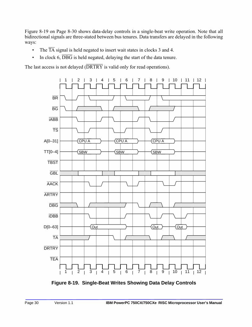
Figure 8-19 on Page 8-30 shows data-delay controls in a single-beat write operation. Note that allbidirectional signals are three-stated between bus tenures. Data transfers are delayed in the followingways:
• The TA signal is held negated to insert wait states in clocks 3 and 4.• In clock 6, DBG is held negated, delaying the start of the data tenure.
The last access is not delayed (DRTRY is valid only for read operations).
Figure 8-19. Single-Beat Writes Showing Data Delay Controls
BR
BG
iABB
TS
A[0–31]
TT[0–4]
TBST
GBL
AACK
ARTRY
DBG
iDBB
D[0–63]
TA
DRTRY
TEA
1 2 3 4 5 6 7 8 9 10 11 12
1 2 3 4 5 6 7 8 9 10 11 12
CPU A CPU A CPU A
SBW SBW SBW
Out Out Out
Page 3
0 Vers ion 1.1 IBM PowerPC 750CX/750 CXe RISC Mic roprocessor User’s Manual
Figure 8-20 on Page 8-31 shows the use of data-delay controls with burst transfers. Note that allbidirectional signals are three-stated between bus tenures. Note the following:
• The first data beat of bursted read data (clock 0) is the critical quad word.• The write burst shows the use of TA signal negation to delay the third data beat.• The final read burst shows the use of DRTRY on the third data beat.• The address for the third transfer is delayed until the first transfer completes.
Figure 8-20. Burst Transfers with Data Delay Controls
BR
BG
iABB
TS
A[0–31]
TT[0–4]
TBST
GBL
AACK
ARTRY
DBG
iDBB
D[0–63]
TA
DRTRY
TEA
CPU A
In
1 2 3 4 5 6 7 8 9 10 11 12 13 14 15 16 17 18 19 20
1 2 3 4 5 6 7 8 9 10 11 12 13 14 15 16 17 18 19 20
CPU A CPU A
Read Write Read
In In In Out Out Out 2 Out In In In InIn
Ta
ble of Contents 5/9/02 Page 31
Figure 8-21 on Page 8-32 shows the use of the TEA signal. Note that all bidirectional signals arethree-stated between bus tenures. Note the following:
• The first data beat of the read burst (in clock 0) is the critical quad word.• The TEA signal truncates the burst write transfer on the third data beat.• The 750CX eventually causes an exception to be taken on the TEA event.
Figure 8-21. Use of Transfer Error Acknowledge (TEA)
BR
BG
iABB
TS
A[0–31]
TT[0–4]
TBST
GBL
AACK
ARTRY
DBG
iDBB
D[0–63]
TA
DRTRY
TEA
CPU A
In
1 2 3 4 5 6 7 8 9 10 11 12 13 14 15 16 17
CPU A CPU A
Read Write Read
In In In Out Out Out In In InIn
1 2 3 4 5 6 7 8 9 10 11 12 13 14 15 16 17
Page 32
Version 1.1 IBM PowerPC 750 CX/750CX e R ISC Micro processor User’s Manual
8.6 No-DRTRY Bus Configuration(DRTRY is optional on the 750CX)
The 750CX is internally configured for the no-DRTRY mode. The no-DRTRY mode allows theforwarding of data during load operations to the internal CPU one bus cycle sooner than in the normalbus protocol.
The 60x bus protocol specifies that, during load operations, the memory system normally has thecapability to cancel data that was read by the master on the bus cycle after TA was asserted. This latecancellation protocol requires the 750CX to hold any loaded data at the bus interface for oneadditional bus clock to verify that the data is valid before forwarding it to the internal CPU. The750CX uses the no-DRTRY mode that eliminates this one-cycle stall during all load operations, andallows for the forwarding of data to the internal CPU immediately when TA is recognized.
The data can no longer be cancelled the cycle after it is acknowledged by an assertion of TA. Data isimmediately forwarded to the CPU internally, and any attempt at late cancellation by the system maycause improper operation by the 750CX.
When a typical 60x PowerPC processor is following normal bus protocol, data may be cancelled thebus cycle after TA by either of two means—late cancellation by DRTRY, or late cancellation byARTRY. For the 750CX, due to the default no-DRTRY mode, both late cancellation cases must bedisallowed in the system design for the bus protocol. The system must also ensure that an assertionof ARTRY by a snooping device must occur before or coincident with the first assertion of TA to the750CX, but not on the cycle after the first assertion of TA.
8.7 32-bit Data Bus ModeThe 750CX supports an optional 32-bit data bus mode. The 32-bit data bus mode operates the sameas the 64-bit data bus mode with the exception of the byte lanes involved in the transfer and thenumber of data beats that are performed. When in 32-bit data bus mode, only byte lanes 0 through 3are used corresponding to DH0–DH31 and DP0–DP3. Byte lanes 4 through 7 corresponding toDL0–DL31 and DP4–DP7 are never used in this mode. The unused data bus signals are not sampledby the 750CX during read operations, and they are driven low during write operations.
The number of data beats required for a data tenure in the 32-bit data bus mode is one, two, or eightbeats depending on the size of the program transaction and the cache mode for the address. Datatransactions of one or two data beats are performed for caching-inhibited load/store or write-throughstore operations. These transactions do not assert the TBST signal even though a two-beat burst maybe performed (having the same TBST and TSIZ[0–2] encodings as the 64-bit data bus mode).Single-beat data transactions are performed for bus operations of 4 bytes or less, and double-beat datatransactions are performed for 8-byte operations only. The 750CX only generates an 8-byte operationfor a double-word-aligned load or store double operation to or from the floating-point registers. Allcache-inhibited instruction fetches are performed as word (single-beat) operations.
Data transactions of eight data beats are performed for burst operations that load into or store fromthe 750CX’s internal caches. These transactions transfer 32 bytes in the same way as in 64-bit databus mode, asserting the TBST signal, and signaling a transfer size of 2 (TSIZ(0–2) = 0b010).
The same bus protocols apply for arbitration, transfer, and termination of the address and data tenuresin the 32-bit data bus mode as they apply to the 64-bit data bus mode. Late ARTRY cancellation ofthe data tenure applies on the bus clock after the first data beat is acknowledged (after the first TA)for word or smaller transactions, or on the bus clock after the second data beat is acknowledged (after
Table of Contents 5/9/02 Page 33

the second TA) for double-word or burst operations (or coincident with respective TA if no-DRTRYmode is selected).
An example of an eight-beat data transfer while the 750CX is in 32-bit data bus mode is shown inFigure 8-22.
Figure 8-22. 32-Bit Data Bus Transfer (Eight-Beat Burst)
An example of a two-beat data transfer is shown in Figure 8-23.
Figure 8-23. 32-Bit Data Bus Transfer (Two-Beat Burst with DRTRY)
TS
ABB
ADDR
TBST
AACK
ARTRY
DBB
DH[0–31]
TA
DRTRY
TEA
0 1 2 3 4 5 6 7
TS
ABB
ADDR
TBST
AACK
ARTRY
DBB
DH[0–31]
TA
DRTRY
TEA
0 1
Page 34 Version 1.1 IBM PowerPC 750CX/750CXe RISC Microprocessor User’s Manual

The 750CX selects 64-bit or 32-bit data bus mode at start-up by sampling the state of the QACKsignal at the negation of HRESET. If the QACK signal is asserted at the negation of HRESET, 64-bitdata mode is selected by the 750CX. If QACK is de-asserted at the negation of HRESET, 32-bit datamode is selected. Table 8-5 describes the burst ordering when the 750CX is in 32-bit mode.
The aligned data transfer cases for 32-bit data bus mode are shown in Table 8-6. All of the transfersrequire a single data beat (if caching-inhibited or write-through) except for double-word cases whichrequire two data beats. The double-word case is only generated by the 750CX for load or store doubleoperations to/from the floating-point registers. All caching-inhibited instruction fetches areperformed as word operations.
Table 8-5. Burst Ordering—32-Bit Bus
Data TransferFor Starting Address
A[27–28] = 00 A[27–28] = 01 A[27–28] = 10 A[27–28] = 11
First data beat DW0-U DW1-U DW2-U DW3-U
Second data beat DW0-L DW1-L DW2-L DW3-L
Third data beat DW1-U DW2-U DW3-U DW0-U
Fourth data beat DW1-L DW2-L DW3-L DW0-L
Fifth data beat DW2-U DW3-U DW0-U DW1-U
Sixth data beat DW2-L DW3-L DW0-L DW1-L
Seventh data beat DW3-U DW0-U DW1-U DW2-U
Eighth data beat DW3-L DW0-L DW1-L DW2-L
Notes: A[29–31] are always 0b000 for burst transfers by the 750CX.
“U” and “L” represent the upper and lower word of the double word respectively.
Table of Contents 5/9/02 Page 35

Misaligned data transfers in the 32-bit bus mode is the same as in the 64-bit bus mode with theexception that only DH[0-31] data lines are used. Table 8-7 on Page 8-37 shows examples of 4-bytemisaligned transfers starting at each possible byte address within a double word.
Table 8-6. Aligned Data Transfers (32-Bit Bus Mode)
Transfer Size TSIZ0 TSIZ1 TSIZ2 A[29–31]Data Bus Byte Lane(s)
0 1 2 3 4 5 6 7
Byte 0 0 1 000 A — — — x x x x
0 0 1 001 — A x — x x x x
0 0 1 010 — — A — x x x x
0 0 1 011 — — — A x x x x
0 0 1 100 A — — — x x x x
0 0 1 101 — A — — x x x x
0 0 1 110 — — A — x x x x
0 0 1 111 — — — A x x x x
Half word 0 1 0 000 A A — — x x x x
0 1 0 010 — — A A x x x x
0 1 0 100 A A — — x x x x
0 1 0 110 — — A A x x x x
Word 1 0 0 000 A A A A x x x x
1 0 0 100 A A A A x x x x
Double word
Second beat
0 0 0 000 A A A A x x x x
0 0 0 000 A A A A x x x x
Notes:
A: Byte lane used—: Byte lane not usedx: Byte lane not used in 32-bit bus mode
Page 36 Version 1.1 IBM PowerPC 750CX/750CXe RISC Microprocessor User’s Manual

8.8 Interrupt, Checkstop, and Reset SignalsThis section describes external interrupts, checkstop operations, and hard and soft reset inputs.
8.8.1 External InterruptsThe external interrupt input signals (INT and MCP) of the 750CX eventually force the processor totake the external interrupt vector if the MSR[EE] is set, or the machine check interrupt if theMSR[ME] and the HID0[EMCP] bits are set.
8.8.2 CheckstopsA checkstop causes the processor to halt. Once the 750CX enters a checkstop state, only a hard resetcan clear the processor from the checkstop state.
Table 8-7. Misaligned 32-Bit Data Bus Transfer (Four-Byte Examples)
Transfer Size(Four Bytes)
TSIZ[0–2] A[29–31]Data Bus Byte Lanes
0 1 2 3 4 5 6 7
Aligned 1 0 0 0 0 0 A A A A x x x x
Misaligned—first access
second access
0 1 1 0 0 1 A A A x x x x
0 0 1 1 0 0 A — — — x x x x
Misaligned—first access
second access
0 1 0 0 1 0 — — A A x x x x
0 1 0 1 0 0 A A — x x x x x
Misaligned—first access
second access
0 0 1 0 1 1 — — — A x x x x
0 1 1 1 0 0 A A A — x x x x
Aligned 1 0 0 1 0 0 A A A A x x x x
Misaligned—first access
second access
0 1 1 1 0 1 — A A A x x x x
0 0 1 0 0 0 A — — — x x x x
Misaligned—first access
second access
0 1 0 1 1 0 — — A A x x x x
0 1 0 0 0 0 A A — — x x x x
Misaligned—first access
second access
0 0 1 1 1 1 — — — A x x x x
0 1 1 0 0 0 A A A — x x x x
Notes:
A: Byte lane used—: Byte lane not usedx: Byte lane not used in 32-bit bus mode
Table of Contents 5/9/02 Page 37

The 750CX has two checkstop input signals—CKSTP_IN (nonmaskable) and MCP (enabled whenMSR[ME] is cleared, and HID0[EMCP] is set). If CKSTP_IN or MCP is asserted, the 750CX haltsoperations by gating off all internal clocks.
Following is the list of checkstop sources.
• Machine Check with MSR(ME)=0. If MSR(ME)=0 when a machine check interrupt occurs, then the checkstop state is entered. The machine check sources are as follows. — TEA_ assertion on the 60X bus — Address parity error on the 60X bus — Data parity error on the 60X bus — Data double bit error on the L2 bus
• Machine check input pin (MCP_) • Checkstop input pin (CKSTP_IN_)
8.8.3 Reset InputsThe 750CX has two reset inputs, described as follows:
• HRESET (hard reset)—The HRESET signal is used for power-on reset sequences, or for situations in which the 750CX must go through the entire cold start sequence of internal hardware initialization.
• SRESET (soft reset)—The soft reset input provides warm reset capability. This input can be used to avoid forcing the 750CX to complete the cold start sequence.
When either HRESET is negated or SRESET transitions to asserted, the processor attempts to fetchcode from the system reset exception vector. The vector is located at offset 0x00100 from theexception prefix (all zeros or ones, depending on the setting of the exception prefix bit in the machinestate register (MSR[IP]). The MSR[IP] bit is set for HRESET.
8.8.4 System Quiesce Control SignalsThe system quiesce control signals (QREQ and QACK) allow the processor to enter the nap or sleeplow-power states, and bring bus activity to a quiescent state in an orderly fashion.
Prior to entering the nap or sleep power state, the 750CX asserts the QREQ signal. This signal allowsthe system to terminate or pause any bus activities that are normally snooped. When the system isready to enter the system quiesce state, it asserts the QACK signal. At this time the 750CX may entera quiescent (low power) state. When the 750CX is in the quiescent state, it stops snooping busactivity. While the 750CX is in the nap power state, the system power controller can enable snoopingby the 750CX by deasserting the QACK signal for at least eight bus clock cycles, after which the750CX is capable of snooping bus transactions. The reassertion of QACK following the snooptransactions will cause the 750CX to reenter the nap power state.
Page 38 Version 1.1 IBM PowerPC 750CX/750CXe RISC Microprocessor User’s Manual

8.9 Processor State SignalsThis section describes the 750CX's support for atomic update and memory through the use of thelwarx/stwcx. opcode pair, and includes a description of the TLBISYNC input.
8.9.1 Support for the lwarx/stwcx. Instruction PairThe Load Word and Reserve Indexed (lwarx) and the Store Word Conditional Indexed (stwcx.)instructions provide a means for atomic memory updating. Memory can be updated atomically bysetting a reservation on the load and checking that the reservation is still valid before the store isperformed. In the 750CX, the reservations are made on behalf of aligned, 32-byte sections of thememory address space.
8.9.2 TLBISYNC Input (Optional on the 750CX)Note: The TLBISYNC pin is not connected in the 750CX, so the corresponding MMUsynchronization function is effectively disabled.
8.10 IEEE 1149.1a-1993 Compliant InterfaceThe 750CX boundary-scan interface is a fully-compliant implementation of the IEEE 1149.1a-1993standard. This section describes the 750CX’s IEEE 1149.1a-1993 (JTAG) interface.
8.10.1 JTAG/COP InterfaceThe 750CX has extensive on-chip test capability including the following:
• Debug control/observation (COP)• Boundary scan (standard IEEE 1149.1a-1993 (JTAG) compliant interface)• Support for manufacturing test
The COP and boundary scan logic are not used under typical operating conditions. Detaileddiscussion of the 750CX test functions is beyond the scope of this document; however, sufficientinformation has been provided to allow the system designer to disable the test functions that wouldimpede normal operation.
The JTAG/COP interface is shown in Figure 8-24. For more information, refer to IEEE Standard TestAccess Port and Boundary Scan Architecture IEEE STD 1149-1a-1993.
Figure 8-24. IEEE 1149.1a-1993 Compliant Boundary Scan Interface
TDI (Test Data Input)
TMS (Test Mode Select)
TCK (Test Clock Input)
TDO (Test Data Output)
TRST (Test Reset)
Table of Contents 5/9/02 Page 39

Page 40 Version 1.1 IBM PowerPC 750CX/750CXe RISC Microprocessor User’s Manual

Chapter 9 L2 Cache This chapter describes 750CX microprocessor‘s implementation of 256K byte, L2 cache.
9.1 L2 Cache OverviewThe 750CX’s L2 cache is implemented with an on-chip, two-way set-associative tag memory with2048 tags per way, and an on-chip 256 Kbyte SRAM for data storage. The tags are sectored to supporttwo cache blocks per tag entry (two sectors, 64 bytes). Each sector (32-byte L1 cache block) in theL2 cache has its own valid and modified bits. In addition, the SRAM includes an 8-bit ECC for everydouble word. The ECC logic corrects most single-bit errors and detects double bit errors as data isread from the SRAM. The L2 cache maintains cache coherency through snooping and is normallyconfigured to operate in copy-back mode.
The L2 cache control register (L2CR) allows control of:
• L2 cache configuration
• Double bit error machine check
• Global invalidation of L2 contents
• Write-through operation
• L2 test support
9.1.1 L2 Cache OperationThe 750CX’s L2 cache is a combined instruction and data cache that receives memory requests fromboth L1 instruction and L1 data caches independently. The L1 requests are generally the result ofinstruction fetch misses, data load or store misses, write-through operations, or cache managementinstructions. Each L1 request generates an address lookup in the L2 tags. If a hit occurs, theinstructions or data are forwarded to the L1 cache. A miss in the L2 tags causes the L1 request to beforwarded to the 60x bus interface. The cache block received from the bus is forwarded to the L1cache immediately, and is also loaded into the L2 cache with the tag marked valid and unmodified. Ifthe cache block loaded into the L2 causes a new tag entry to be allocated and the current tag entry ismarked valid modified, the modified sectors of the tag to be replaced are castout from the L2 cacheto the 60x bus.
At any given time the L1 instruction cache may have one instruction fetch request, and the L1 datacache may have one load and two stores requesting L2 cache access. The L2 cache also services snooprequests from the 60x bus. When there are multiple pending requests to the L2 cache, snoop requestshave highest priority, followed by data load and store requests (serviced on a first-in, first-out basis).Instruction fetch requests have the lowest priority in accessing the L2 cache when there are multipleaccesses pending.
If read requests from both the L1 instruction and L1 data caches are pending, the L2 cache canperform hit-under-miss and supplies the available instruction or data while a bus transaction for theprevious L2 cache miss is being performed. The L2 cache does not support miss-under-miss, and thesecond instruction fetch or data load stalls until the bus operation resulting from the first L2 misscompletes
Table of Contents 5/9/02 Page 1
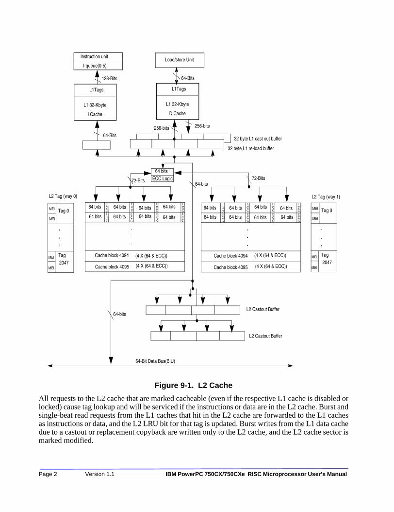
Figure 9-1. L2 Cache
All requests to the L2 cache that are marked cacheable (even if the respective L1 cache is disabled orlocked) cause tag lookup and will be serviced if the instructions or data are in the L2 cache. Burst andsingle-beat read requests from the L1 caches that hit in the L2 cache are forwarded to the L1 cachesas instructions or data, and the L2 LRU bit for that tag is updated. Burst writes from the L1 data cachedue to a castout or replacement copyback are written only to the L2 cache, and the L2 cache sector ismarked modified.
Load/store Unit
72-Bits
L2 Castout Buffer
64-Bit Data Bus(BIU)
64 bits
L1Tags
L1 32-Kbyte
D Cache
L2 Tag (way 0)
Tag 0
Tag
2047
.
..
MEI
MEI
MEI
MEI
Cache block 4095
Cache block 4094
.
.
.
L2 Tag (way 1)
Tag 0
Tag
2047
.
MEI
MEI
MEI
MEI
Cache block 4095
Cache block 4094
.
.
.
ECC Logic
256-bits
64-bits
L2 Castout Buffer
ECC
ECCECC
ECC
ECC
ECCECC
ECC
ECC
64 bits
64 bits
64 bits
64 bits
64 bits
64 bits
64 bits 64 bits
ECC
64 bits ECC
64 bits ECC
64 bits
ECC
64 bits ECC
64 bits ECC
64 bits
ECC64 bits
(4 X (64 & ECC))
(4 X (64 & ECC))
(4 X (64 & ECC))
(4 X (64 & ECC))
72-Bits
64-Bits
L1Tags
L1 32-Kbyte
I Cache
Instruction unit
I-queue(0-5)
64 bits
128-Bits
64-Bits
64-bits
.
.
32 byte L1 cast out buffer
256-bits
32 byte L1 re-load buffer
Page 2 Version 1.1 IBM PowerPC 750CX/750CXe RISC Microprocessor User’s Manual

If the L2 cache is configured as write-through, the L2 sector is marked unmodified, and the write isforwarded to the 60x bus. If the L1 castout requires a new L2 tag entry to be allocated and the currenttag is marked modified, any modified sectors of the tag to be replaced are cast out of the L2 cache tothe 60x bus.
Single-beat read requests from the L1 caches that miss in the L2 cache do not cause any state changesin the L2 cache and are forwarded on the 60x bus interface. Cacheable single-beat store requestsmarked copy-back that hit in the L2 are allowed to update the L2 cache sector, but do not cause L2cache sector allocation or deallocation. Cacheable, single-beat store requests that miss in the L2 areforwarded to the 60x bus. Single-beat store requests marked write-through (through addresstranslation or through the configuration of L2CR[L2WT]) are written to the L2 cache if they hit andare written to the 60x bus independent of the L2 hit/miss status. If the store hits in the L2 cache, themodified/unmodified status of the tag remains unchanged. All requests to the L2 cache that aremarked cache-inhibited by address translation (through either the MMU or by default WIMGconfiguration) bypass the L2 cache and do not cause any L2 cache tag state change.
The execution of the stwcx. instruction results in single-beat writes from the L1 data cache. Thesesingle-beat writes are processed by the L2 cache according to hit/miss status, L1 and L2 write-throughconfiguration, and reservation-active status. If the address associated with the stwcx. instructionmisses in the L2 cache or if the reservation is no longer active, the stwcx. instruction bypasses the L2cache and is forwarded to the 60x bus interface. If the stwcx. hits in the L2 cache and the reservationis still active, one of the following actions occurs:
• If the stwcx. hits a modified sector in the L2 cache (independent of write-through status), or if the stwcx. hits both the L1 and L2 caches in copy-back mode, the stwcx. is written to the L2 and the reservation completes.
• If the stwcx. hits an unmodified sector in the L2 cache, and either the L1 or L2 is in write-through mode, the stwcx. is forwarded to the 60x bus interface and the sector hit in the L2 cache is invalidated.
L1 cache-block-push operations generated by the execution of dcbf and dcbst instructions writethrough to the 60x bus interface and invalidate the L2 cache sector if they hit. The execution of dcbfand dcbst instructions that do not cause a cache-block-push from the L1 cache are forwarded to theL2 cache to perform a sector invalidation and/or push from the L2 cache to the 60x bus as required.If the dcbf and dcbst instructions do not cause a sector push from the L2 cache, they are forwardedto the 60x bus interface for address-only broadcast if HID0[ABE] is set to 1.
The L2 flush mechanism is similar to the L1 data cache flush mechanism. L2 flush requires that theentire L1 data cache be flushed prior to flushing the L2 cache. Also, interrupts must be disabledduring the L2 flush so that the LRU algorithm does not get disturbed. The L2 can be flushed byexecuting uniquely addressed load instructions to each of the 32 byte blocks of the L2 cache. Thisrequires a load to each of the 2 sets (2-way set associative) of the 32-byte block (sector) within each64-byte line of the L2 cache. The loads must not hit in the L1 cache in order to effect a flush of theL2 cache.
The dcbi instruction is always forwarded to the L2 cache and causes a segment invalidation if a hitoccurs. The instruction is also forwarded to the 60x bus interface for broadcast if HID0[ABE] is setto 1. The icbi instruction invalidates only L1 cache blocks and is never forwarded to the L2 cache.
Table of Contents 5/9/02 Page 3

Any dcbz instructions marked global do not affect the L2 cache state. If an instruction hits in the L1and L2 caches, the L1 data cache block is cleared and the instruction completes. If an instructionmisses in the L2 cache, it is forwarded to the 60x bus interface for broadcast. Any dcbz instructionsthat are marked nonglobal act only on the L1 data cache without reference to the state of the L2.
The sync and eieio instructions bypass the L2 cache and are forwarded to the 60x bus.
9.1.2 L2 Cache Control Register (L2CR)The L2 cache control register is used to configure and enable the L2 cache. The L2CR is asupervisor-level read/write, implementation-specific register that is accessed as SPR 1017. Thecontents of the L2CR are cleared during power-on reset. Table 9-8 describes the L2CR bits. Foradditional information about the configuration of the L2CR, refer to Section 2.1.5 on Page 2-21.
9.1.3 L2 Cache InitializationFollowing a power-on or hard reset, the L2 cache is disabled initially. Before enabling the L2 cache,other configuration parameters must be set in the L2CR, and the L2 tags must be globally invalidated.The L2 cache should be initialized during system start-up.
Table 9-8. L2 Cache Control Register
Bit Name Function Notes
0 L2E L2 enable
1 L2CE L2 double bit error checkstop enable.
2-8 Reserved. 1
9 L2DO L2 data-only. Setting this bit inhibits the caching of instructions in the L2 cache. All accesses from the L1 instruction cache are treated as cache-inhibited by the L2 cache (bypass L2 cache, no L2 tag look-up performed).
10 L2I L2 global invalidate. Setting L2I invalidates the L2 cache globally by clearing the L2 status bits.
11 Reserved 1
12 L2WT L2 write-through. Setting L2WT selects write-through mode (rather than the default copy-back mode) so all writes to the L2 cache also write through to the 60x bus.
13 L2TS L2 test support. Setting L2TS causes cache block pushes from the L1 data cache that result from dcbf and dcbst instructions to be written only into the L2 cache and marked valid, rather than being written only to the 60x bus and marked invalid in the L2 cache in case of hit. If L2TS is set, causes single-beat store operations that miss in the L2 cache to be discarded.
14-30 Reserved. 1
31 L2IP L2 global invalidate in progress (read only)—This read-only bit indicates whether an L2 global invalidate is occurring.
Notes:1. The reserved bits are considered as “don’t care” even though these bits can be written and read.
Page 4 Version 1.1 IBM PowerPC 750CX/750CXe RISC Microprocessor User’s Manual

The sequence for initializing the L2 cache is as follows.
1. Power-on reset (automatically performed by the assertion of HRESET signal).
2. Disable interrupts and Dynamic Power Management (DPM).
3. Disable L2 cache by clearing L2CR[L2E].
4. Perform an L2 global invalidate as described in the next section.
5. After the L2 global invalidate has been performed, and the other L2 configuration bits have been set, enable the L2 cache for normal operation by setting the L2CR[L2E] bit to 1.
9.1.4 L2 Cache Global InvalidationThe L2 cache supports a global invalidation function in which all bits of the L2 tags (tag data bits, tagstatus bits, and LRU bit) are cleared. It is performed by an on-chip hardware state machine thatsequentially cycles through the L2 tags. The global invalidation function is controlled through theL2CR[L2I], and it must be performed only while the L2 cache is disabled. The 750CX can continueoperation during a global invalidation provided the L2 cache has been properly disabled before theglobal invalidation operation starts.
The sequence for performing a global invalidation of the L2 cache is as follows:
1. Execute a sync instruction to finish any pending store operations in the load/store unit, disable the L2 cache by clearing L2CR[L2E], and execute an additional sync instruction after disabling the L2 cache to ensure that any pending operations in the L2 cache unit have completed.
2. Initiate the global invalidation operation by setting the L2CR[L2I] bit to 1.
3. Monitor the L2CR[L2IP] bit to determine when the global invalidation operation is complete (indicated by the clearing of L2CR[L2IP]). The global invalidation requires approximately 32K core clock cycles to complete.
4. After detecting the clearing of L2CR[L2IP], clear L2CR[L2I] and re-enable the L2 cache for normal operation by setting L2CR[L2E].
5. Never perform a global invalidation of the L2 cache while in dynamic power management enable mode. Be sure the HID0[DPM] bit is zero. Also ensure that the processor is in a tight uninterruptable software loop monitoring the end of the global invalidate, so that an L1 data cache miss cannot occur that would initiate a reload from system memory during the global invalidate operation.
9.1.5 L2 Cache Test Features and MethodsIn the course of system power-up, testing may be required to verify the proper operation of the L2 tagmemory, SRAM, and overall L2 cache system. The following sections describe the 750CX’s featuresand methods for testing the L2 cache. The L2 cache address space should be marked as guarded (G= 1) so spurious load operations are not forwarded to the 60x bus interface before branch resolutionduring L2 cache testing.
Table of Contents 5/9/02 Page 5

9.1.5.1 L2CR Support for L2 Cache TestingL2CR[DO] and L2CR[TS] support the testing of the L2 cache. L2CR[DO] prevents instructions frombeing cached in the L2. This allows the L1 instruction cache to remain enabled during the testingprocess without having L1 instruction misses affect the contents of the L2 cache and allows all L2cache activity to be controlled by program-specified load and store operations.
L2CR[TS] is used with the dcbf and dcbst instructions to push data into the L2 cache. WhenL2CR[TS] is set, and the L1 data cache is enabled, an instruction loop containing a dcbf instructioncan be used to store any address or data pattern to the L2 cache. Additionally, 60x bus broadcastingis inhibited when a dcbz instruction is executed. This allows the use of a dcbz instruction to clear anL1 cache block, followed by a dcbf instruction to push the cache block into the L2 cache andinvalidate the L1 cache block.
When the L2 cache is enabled, cacheable single-beat read operations are allowed to hit in the L2 cacheand cacheable write operations are allowed to modify the contents of the L2 cache when a hit occurs.Cacheable single-beat read and writes occur when address translation is disabled (invoking the use ofthe default WIMG bits (0b0011)), or when address translation is enabled and accesses are marked ascacheable through the page table entries or the BATs, and the L1 data cache is disabled or locked.When the L2 cache has been initialized and the L1 cache has been disabled or locked, load or storeinstructions then bypass the L1 cache and hit in the L2 cache directly. When L2CR[TS] is set,cacheable single-beat writes are inhibited from accessing the 60x bus interface after an L2 cache miss.
During L2 cache testing, the performance monitor can be used to count L2 cache hits and misses,thereby providing a numerical signature for test routines and a way to verify proper L2 cacheoperation.
9.1.5.2 L2 Cache TestingA typical test for verifying the proper operation of the 750CX’s L2 cache memory would perform thefollowing steps.
1. Initialize the L2 test sequence by disabling address translation to invoke the default WIMG setting (0b0011). Set L2CR[DO] and L2CR[TS] and perform a global invalidation of the L1 data cache and the L2 cache. The L1 instruction cache can remain enabled to improve execution efficiency.
2. Test the L2 cache SRAM by enabling the L1 data cache and executing a sequence of dcbz, stw, and dcbf instructions to initialize the L2 cache with a desired range of consecutive addresses and with cache data consisting of zeros. Once the L2 cache holds a sequential range of addresses, disable the L1 data cache and execute a series of single-beat load and store operations employing a variety of bit patterns to test for stuck bits and pattern sensitivities in the L2 cache SRAM. The performance monitor can be used to verify whether the number of L2 cache hits or misses corresponds to the tests performed.
3. Test the L2 cache tag memory by enabling the L1 data cache and executing a sequence of dcbz, stw, and dcbf instructions to initialize the L2 cache with a wide range of addresses and cache data. Once the L2 cache is populated with a known range of addresses and data, disable the L1 data cache and execute a series of store operations to addresses not previously in the L2 cache. These store operations should miss in every case. Note that setting the L2CR[TS] inhibits L2 cache misses from being forwarded to the 60x bus interface, thereby avoiding the potential for bus errors due to addressing hardware or nonexistent memory. The L2 cache then
Page 6 Version 1.1 IBM PowerPC 750CX/750CXe RISC Microprocessor User’s Manual

can be further verified by reading the previously loaded addresses and observing whether all the tags hit, and that the associated data compares correctly. The performance monitor can also be used to verify whether the proper number of L2 cache hits and misses correspond to the test operations performed.
4. The entire L2 cache can be tested by clearing L2CR[DO] and L2CR[TS], restoring the L1 and L2 caches to their normal operational state, and executing a comprehensive test program designed to exercise all the caches. The test program should include operations that cause L2 hit, reload, and castout activity that can be subsequently verified through the performance monitor.
9.1.6 L2 Cache TimingThere is a 64-bit bus to access the L2 SRAM. Accesses to the L2 cache are controlled by a three cyclefinite state machine. To write into the L2 cache the address is presented on the first cycle while correctECC codes are being generated for the data. On the second cycle the data and ECC codes are writteninto the L2 SRAMS and the third cycle is not used. For read access to the L2 data cache the addressis presented on the first cycle. On the second cycle the SRAMS are accessed. On the third cycle theECC codes are checked and data corrected for most single bit errors. On the fourth cycle the data isforwarded to the requesting unit. If data is uncorrectable by the ECC code a parity error and machinecheck is generated.
Cache line transfers from the L2 to the L1 are pipelined and require a total of seven cycles. The criticaldouble word is transferred first with wrap around to complete the transfer of the cache line. Theaddress of the critical double is presented on the first cycle. This double word is transferred on theforth cycle and the next three double words are transfer during the next three cycles.
Individual (separate) accesses to the L2 cache are not pipelined.
Table of Contents 5/9/02 Page 7

Page 8 Version 1.1 IBM PowerPC 750CX/750CXe RISC Microprocessor User’s Manual

Chapter 10 Power and Thermal Management100100
The 750CX microprocessor is specifically designed for low-power operation. It provides bothautomatic and program-controlled power reduction modes for progressive reduction of powerconsumption. It also provides a thermal assist unit (TAU) to allow on-chip thermal measurement,allowing sophisticated thermal management for high-performance portable systems. This chapterdescribes the hardware support provided by the 750CX for power and thermal management.
10.1 Dynamic Power ManagementIMPLEMENTATION NOTE:
The Dynamic Power Management (DPM) feature, using HID0[DPM], is only supported in the DD2.4 and DD3.1 revisions of the 750CX. The HID0[DM] setting is not used by the other 750CX revisions. Please refer to the specific Errata document for revision level data.
Dynamic power management (DPM) automatically powers up and down the individual executionunits of the 750CX, based upon the contents of the instruction stream. For example, if nofloating-point instructions are being executed, the floating-point unit is automatically powered down.Power is not actually removed from the execution unit; instead, each execution unit has anindependent clock input, which is automatically controlled on a clock-by-clock basis. Since CMOScircuits consume negligible power when they are not switching, stopping the clock to an executionunit effectively eliminates its power consumption. The operation of DPM is completely transparentto software or any external hardware. Dynamic power management is enabled by setting HID0[DPM]to 1.
10.2 Programmable Power ModesThe 750CX provides four programmable power states—full power, doze, nap, and sleep. Softwareselects these modes by setting one (and only one) of the three power saving mode bits in the HID0register.
Hardware can enable a power management state through external asynchronous interrupts. Such ahardware interrupt causes the transfer of program flow to interrupt handler code that then invokes theappropriate power saving mode. The 750CX also contains a decrementer which allows it to enter thenap or doze mode for a predetermined amount of time and then return to full power operation througha decrementer interrupt.
NOTE: The 750CX cannot switch from one power management mode to another without first returning to full-power mode.
The sleep mode disables bus snooping; therefore, a hardware handshake is provided to ensurecoherency before the 750CX enters this power management mode.
Table of Contents 5/9/02 Page 1

Table 10-1 summarizes the four power states.
10.2.1 Power Management ModesThe following sections describe the characteristics of the 750CX’s power management modes, therequirements for entering and exiting the various modes, and the system capabilities provided by the750CX while the power management modes are active.
10.2.1.1 Full-Power ModeFull-power mode is selected when the POW bit in MSR is cleared.
• Default state following power-up and HRESET
• All functional units are operating at full processor speed at all times.
10.2.1.2 Doze ModeDoze mode disables most functional units but maintains cache coherency by enabling the businterface unit and snooping. A snoop hit causes the 750CX to enable the data cache, copy the databack to memory, disable the cache, and fully return to the doze state.
• Most functional units disabled
• Bus snooping and time base/decrementer still enabled
• Doze mode sequence
— Set doze bit (HID0[8] = 1), clear nap and sleep bits (HID0[9] and HID0[10] = 0)
— 750CX enters doze mode after several processor clocks
• Several methods of returning to full-power mode
— Assert INT, MCP, decrementer, performance monitor, machine check, or thermal management interrupts
— Assert hard reset or soft reset
Table 10-1. 750CX Microprocessor Programmable Power Modes
PM Mode Functioning Units Activation Method Full-Power Wake Up Method
Full power All units active — —
Doze • Bus snooping• Data cache as needed• Decrementer timer
Controlled by SW External asynchronous exceptions*Decrementer interruptPerformance monitor interruptThermal management interruptHard or soft reset
Nap • Bus snooping — enabled by deassertion
of QACK• Decrementer timer
Controlled by hardware and software
External asynchronous exceptions*Decrementer interruptHard or soft reset
Sleep None Controlled by hardware and software
External asynchronous exceptions*Hard or soft reset
Note: * Exceptions are referred to as interrupts in the architecture specification.
Page 2 Version 1.1 IBM PowerPC 750CX/750CXe RISC Microprocessor User’s Manual

• Transition to full-power state takes no more than a few processor cycles
• PLL running and locked to SYSCLK
10.2.1.3 Nap ModeThe nap mode disables the 750CX but still maintains the phase-locked loop (PLL), and the timebase/decrementer. The time base can be used to restore the 750CX to full-power state after aprogrammed amount of time. To maintain data coherency, bus snooping is disabled for nap and sleepmodes through a hardware handshake sequence using the quiesce request (QREQ) and quiesceacknowledge (QACK) signals. The 750CX asserts the QREQ signal to indicate that it is ready todisable bus snooping. When the system has ensured that snooping is no longer necessary, it will assertQACK and the 750CX will enter the nap mode. If the system determines that a bus snoop cycle isrequired, QACK is deasserted to the 750CX for at least eight bus clock cycles, and the 750CX willthen be able respond to a snoop cycle. Assertion of QACK following the snoop cycle will againdisable the 750CX’s snoop capability. The 750CX’s power dissipation while in nap mode with QACKdeasserted is the same as the power dissipation while in doze mode.
The 750CX also allows dynamic switching between nap and doze modes to allow the use of nap modewithout sacrificing hardware snoop coherency. For this operation, negating QACK at any time for atleast 8 bus cycles guarantees that the 750CX has transitioned from nap mode to doze mode in orderto snoop. Reasserting QACK then allows the 750CX to return to nap mode. This sequencing could beused by the system at any time with knowledge of what power management mode, if any, that the750CX is currently in.
• Time base/decrementer still enabled
• Thermal management unit enabled
• Most functional units disabled
• All nonessential input receivers disabled
• Nap mode sequence
— Set nap bit (HID0[9] = 1), clear doze and sleep bits (HID0[8] and HID0[10] = 0)
— 750CX asserts quiesce request (QREQ) signal
— System asserts quiesce acknowledge (QACK) signal
— 750CX enters nap mode after several processor clocks
• Nap mode bus snoop sequence
— System deasserts QACK signal for eight or more bus clock cycles
— 750CX snoops address tenure(s) on bus
— System asserts QACK signal to restore full nap mode
• Several methods of returning to full-power mode
— Assert INT, MCP, machine check, or decrementer interrupts
— Assert hard reset or soft reset
• Transition to full-power takes no more than a few processor cycles
• PLL running and locked to SYSCLK.
Table of Contents 5/9/02 Page 3

10.2.1.4 Sleep ModeSleep mode consumes the least amount of power of the four modes since all functional units aredisabled. To conserve the maximum amount of power, the PLL may be disabled by placing thePLL_CFG signals in the PLL bypass mode, and disabling SYSCLK.
NOTE: Forcing the SYSCLK signal into a static state does not disable the 750CX’s PLL, which will continue to operate internally at an undefined frequency unless placed in PLL bypass mode.
Due to the fully static design of the 750CX, internal processor state is preserved when no internalclock is present. Because the time base and decrementer are disabled while the 750CX is in sleepmode, the 750CX’s time base contents will have to be updated from an external time base after exitingsleep mode if maintaining an accurate time-of-day is required. Before entering the sleep mode, the750CX asserts the QREQ signal to indicate that it is ready to disable bus snooping.
When the system has ensured that snooping is no longer necessary, it asserts QACK and the 750CXwill enter sleep mode.
• All functional units disabled (including bus snooping and time base)
• All nonessential input receivers disabled
— Internal clock regenerators disabled
— PLL still running (see below)
• Sleep mode sequence
— Set sleep bit (HID0[10] = 1), clear doze and nap bits (HID0[8] and HID0[9])
— 750CX asserts quiesce request (QREQ)
— System asserts quiesce acknowledge (QACK)
— 750CX enters sleep mode after several processor clocks
• Several methods of returning to full-power mode
— Assert INT or MCP interrupts
— Assert hard reset or soft reset
• PLL and DLL may be disabled and SYSCLK may be removed while in sleep mode
• Return to full-power mode after PLL and SYSCLK are disabled in sleep mode
— Enable SYSCLK
— Reconfigure PLL into desired processor clock mode
— System logic waits for PLL start-up and relock time (100 µsecond)
— System logic asserts one of the sleep recovery signals (for example, INT)
Page 4 Version 1.1 IBM PowerPC 750CX/750CXe RISC Microprocessor User’s Manual

10.2.2 Power Management Software ConsiderationsSince the 750CX is a dual-issue processor with out-of-order execution capability, care must be takenin how the power management mode is entered. Furthermore, nap and sleep modes require alloutstanding bus operations to be completed before these power management modes are entered.Normally, during system configuration time, one of the power management modes would be selectedby setting the appropriate HID0 mode bit. Later on, the power management mode is invoked bysetting the MSR[POW] bit. To ensure a clean transition into and out of a power management mode,set the MSR[EE] bit to 1 and execute the following code sequence:
syncmtmsr[POW = 1]isynccontinue
10.3 Thermal Assist UnitWith the increasing power dissipation of high-performance processors and operating conditions thatspan a wider range of temperatures than desktop systems, thermal management becomes an essentialpart of system design to ensure reliable operation of portable systems. One key aspect of thermalmanagement is ensuring that the junction temperature of the microprocessor does not exceed theoperating specification. While the case temperature can be measured with an external thermal sensor,the thermal constant from the junction to the case can be large, and accuracy can be a problem. Thismay lead to lower overall system performance due to the necessary compensation to alleviatemeasurement deficiencies.
The 750CX provides the system designer an efficient means of monitoring junction temperaturethrough the incorporation of an on-chip thermal sensor and programmable control logic to enable athermal management implementation tightly coupled to the processor for improved performance andreliability.
Table of Contents 5/9/02 Page 5
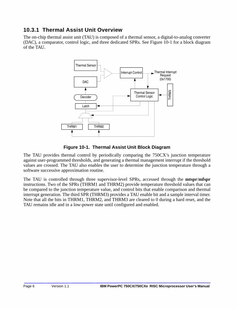
10.3.1 Thermal Assist Unit OverviewThe on-chip thermal assist unit (TAU) is composed of a thermal sensor, a digital-to-analog converter(DAC), a comparator, control logic, and three dedicated SPRs. See Figure 10-1 for a block diagramof the TAU.
Figure 10-1. Thermal Assist Unit Block Diagram
The TAU provides thermal control by periodically comparing the 750CX’s junction temperatureagainst user-programmed thresholds, and generating a thermal management interrupt if the thresholdvalues are crossed. The TAU also enables the user to determine the junction temperature through asoftware successive approximation routine.
The TAU is controlled through three supervisor-level SPRs, accessed through the mtspr/mfsprinstructions. Two of the SPRs (THRM1 and THRM2) provide temperature threshold values that canbe compared to the junction temperature value, and control bits that enable comparison and thermalinterrupt generation. The third SPR (THRM3) provides a TAU enable bit and a sample interval timer.Note that all the bits in THRM1, THRM2, and THRM3 are cleared to 0 during a hard reset, and theTAU remains idle and in a low-power state until configured and enabled.
Thermal Sensor
Thermal SensorControl Logic
DAC
Decoder
Latch
Interrupt Control
THRM1 THRM2
THR
M3
Thermal InterruptRequest(0x1700)
Page 6 Version 1.1 IBM PowerPC 750CX/750CXe RISC Microprocessor User’s Manual

The bit fields in the THRM1 and THRM2 SPRs are described in Table 10-2
.
The bit fields in the THRM3 SPR are described in Table 10-3.
Table 10-2. THRM1 and THRM2 Bit Field Settings
Bits Field Description
0 TIN Thermal management interrupt bit. Read only. This bit is set if the thermal sensor output crosses the threshold specified in the SPR. The state of this bit is valid only if TIV is set. The interpretation of the TIN bit is controlled by the TID bit.
1 TIV Thermal management interrupt valid. Read only. This bit is set by the thermal assist logic to indicate that the thermal management interrupt (TIN) state is valid.
2–8 Threshold Threshold value that the output of the thermal sensor is compared to. The threshold range is between 0° and 127° C, and each bit represents 1° C. Note that this is not the resolution of the thermal sensor.
9–28 — Reserved. System software should clear these bits to 0.
29 TID Thermal management interrupt direction bit. Selects the result of the temperature comparison to set TIN. If TID is cleared to 0, TIN is set and an interrupt occurs if the junction temperature exceeds the threshold. If TID is set to 1, TIN is set and an interrupt is indicated if the junction temperature is below the threshold.
30 TIE Thermal management interrupt enable. Enables assertion of the thermal management interrupt signal. The thermal management interrupt is maskable by the MSR[EE] bit. If TIE is cleared to 0 and THRMn is valid, the TIN bit records the status of the junction temperature vs. threshold comparison without asserting an interrupt signal. This feature allows system software to make a successive approximation to estimate the junction temperature.
31 V SPR valid bit. This bit is set to indicate that the SPR contains a valid threshold, TID, and TIE controls bits. Setting THRM1/2[V] and THRM3[E] to 1 enables operation of the thermal sensor.
Table 10-3. THRM3 Bit Field Settings
Bits Name Description
0–17 — Reserved for future use. System software should clear these bits to 0.
18–30 SITV Sample interval timer value. Number of elapsed processor clock cycles before a junction temperature vs. threshold comparison result is sampled for TIN bit setting and interrupt generation. This is necessary due to the thermal sensor, DAC, and the analog comparator settling time being greater than the processor cycle time. The value should be configured to allow a sampling interval of 20 microseconds.
31 E Enables the thermal sensor compare operation if either THRM1[V] or THRM2[V] is set to 1.
Table of Contents 5/9/02 Page 7

10.3.2 Thermal Assist Unit OperationThe TAU can be programmed to operate in single or dual threshold modes, which results in the TAUgenerating a thermal management interrupt when one or both threshold values are crossed. Inaddition, with the appropriate software routine, the TAU can also directly determine the junctiontemperature. The following sections describe the configuration of the TAU to support these modes ofoperation.
10.3.2.1 TAU Single Threshold ModeWhen the TAU is configured for single threshold mode, either THRM1 or THRM2 can be used tocontain the threshold value, and a thermal management interrupt is generated when the thresholdvalue is crossed. To configure the TAU for single threshold operation, set the desired temperaturethreshold, TID, TIE, and V bits for either THRM1 or THRM2. The unused THRMn threshold SPRshould be disabled by clearing the V bit to 0. In this discussion THRMn refers to the THRM thresholdSPR (THRM1 or THRM2) selected to contain the active threshold value.
After setting the desired operational parameters, the TAU is enabled by setting the THRM3[E] bit to1, and placing a value allowing a sample interval of 20 microseconds or greater in the THRM3[SITV]field. The THRM3[SITV] setting determines the number of processor clock cycles between input tothe DAC and sampling of the comparator output; accordingly, the use of a value smaller thanrecommended in the THRM3[SITV] field can cause inaccuracies in the sensed temperature.
If the junction temperature does not cross the programmed threshold, the THRMn[TIN] bit is clearedto 0 to indicate that no interrupt is required, and the THRMn[TIV] bit is set to 1 to indicate that theTIN bit state is valid. If the threshold value has been crossed, the THRMn[TIN] and THRMn[TIV]bits are set to 1, and a thermal management interrupt is generated if both the THRMn[TIE] andMSR[EE] bits are set to 1.
A thermal management interrupt is held asserted internally until recognized by the 750CX’s interruptunit. Once a thermal management interrupt is recognized, further temperature sampling is suspended,and the THRMn[TIN] and THRMn[TIV] values are held until an mtspr instruction is executed toTHRMn.
The execution of an mtspr instruction to THRMn anytime during TAU operation will clear theTHRMn[TIV] bit to 0 and restart the temperature comparison. Executing an mtspr instruction toTHRM3 will clear both THRM1[TIV] and THRM2[TIV] bits to 0, and restart temperaturecomparison in THRMn if the THRM3[E] bit is set to 1.
Examples of valid THRM1 and THRM2 bit settings are shown in Table 10-4.
Page 8 Version 1.1 IBM PowerPC 750CX/750CXe RISC Microprocessor User’s Manual

10.3.2.2 TAU Dual-Threshold ModeThe configuration and operation of the TAU’s dual-threshold mode is similar to single thresholdmode, except both THRM1 and THRM2 are configured with desired threshold and TID values, andthe TIE and V bits are set to 1. When the THRM3[E] bit is set to 1 to enable temperature measurementand comparison, the first comparison is made with THRM1. If no thermal management interruptresults from the comparison, the number of processor cycles specified in THRM3[SITV] elapses, andthe next comparison is made with THRM2. If no thermal management interrupt results from theTHRM2 comparison, the time specified by THRM3[SITV] again elapses, and the comparison returnsto THRM1.
This sequence of comparisons continues until a thermal management interrupt occurs, or the TAU isdisabled. When a comparison results in an interrupt, the comparison with the threshold SPR causingthe interrupt is halted, but comparisons continue with the other threshold SPR. Following a thermalmanagement interrupt, the interrupt service routine must read both THRM1 and THRM2 to determinewhich threshold was crossed. Note that it is possible for both threshold values to have been crossed,in which case the TAU ceases making temperature comparisons until an mtspr instruction is executedto one or both of the threshold SPRs.
Table 10-4. Valid THRM1 and THRM2 Bit Settings
TIN1 TIV1 TID TIE V Description
x x x x 0 The threshold in the SPR will not be used for comparison.
x x x 0 1 Threshold is used for comparison, thermal management interrupt assertion is disabled.
x x 0 0 1 Set TIN and do not assert thermal management interrupt if the junction temperature exceeds the threshold.
x x 0 1 1 Set TIN and assert thermal management interrupt if the junction temperature exceeds the threshold.
x x 1 0 1 Set TIN and do not assert thermal management interrupt if the junction temperature is less than the threshold.
x x 1 1 1 Set TIN and assert thermal management interrupt if the junction temperature is less than the threshold.
x 0 x x 1 The state of the TIN bit is not valid.
0 1 0 x 1 The junction temperature is less than the threshold and as a result the thermal management interrupt is not generated for TIE = 1.
1 1 0 x 1 The junction temperature is greater than the threshold and as a result the thermal management interrupt is generated if TIE = 1.
0 1 1 x 1 The junction temperature is greater than the threshold and as a result the thermal management interrupt is not generated for TIE = 1.
1 1 1 x 1 The junction temperature is less than the threshold and as a result the thermal management interrupt is generated if TIE = 1.
Note: 1The TIN and TIV bits are read-only status bits.
Table of Contents 5/9/02 Page 9

10.3.2.3 750CX Junction Temperature DeterminationWhile the 750CX’s TAU does not implement an analog-to-digital converter to enable the directdetermination of the junction temperature, system software can execute a simple successiveapproximation routine to find the junction temperature.
The TAU configuration used to approximate the junction temperature is the same required forsingle-threshold mode, except that the threshold SPR selected has its TIE bit cleared to 0 to disablethermal management interrupt generation. Once the TAU is enabled, the successive approximationroutine loads a threshold value into the active threshold SPR, and then continuously polls thethreshold SPRs TIV bit until it is set to 1, indicating a valid TIN bit. The successive approximationroutine can then evaluate the TIN bit value, and then increment or decrement the threshold value foranother comparison. This process is continued until the junction temperature is determined.
10.3.2.4 Power Saving Modes and TAU OperationThe static power saving modes provided by the 750CX (the nap, doze, and sleep modes) allow thetemperature of the processor to be lowered quickly, and can be invoked through the use of the TAUand associated thermal management interrupt. The TAU remains operational in the nap and dozemodes, and in sleep mode as long as the SYSCLK signal input remains active. If the SYSCLK signalis made static when sleep mode is invoked, the TAU is rendered inactive. If the 750CX is enteringsleep mode with SYSCLK disabled, the TAU should be configured to disable thermal managementinterrupts to avoid an unwanted thermal management interrupt when the SYSCLK input signal isrestored.
10.4 Instruction Cache ThrottlingNOTE: The 750CX does not implement dynamic power management (DPM), and therefore does
not provide thermal reduction through instruction cache throttling.
The 750CX provides an instruction cache throttling mechanism to effectively reduce the instructionexecution rate without the complexity and overhead of dynamic clock control. Instruction cachethrottling, when used in conjunction with the TAU and the dynamic power management capability,provides the system designer with a flexible means of controlling device temperature while allowingthe processor to continue operating.
The instruction cache throttling mechanism simply reduces the instruction forwarding rate from theinstruction cache to the instruction dispatcher. Normally, the instruction cache forwards fourinstructions to the instruction dispatcher every clock cycle if all the instructions hit in the cache. Forthermal management the 750CX provides a supervisor-level instruction cache throttling control(ICTC) SPR. The instruction forwarding rate is reduced by writing a nonzero value into the ICTC[FI]field, and enabling instruction cache throttling by setting the ICTC[E] bit to 1. An overall junctiontemperature reduction can result in processors that implement dynamic power management byreducing the power to the execution units while waiting for instructions to be forwarded from theinstruction cache; thus, instruction cache throttling does not provide thermal reduction unlessHID0[DPM] is set to 1.
NOTE: During instruction cache throttling the configuration of the PLL remains unchanged.
Page 10 Version 1.1 IBM PowerPC 750CX/750CXe RISC Microprocessor User’s Manual

The bit field settings of the ICTC SPR are shown in Table 10-5.
Table 10-5. ICTC Bit Field Settings
Bits Name Description
23–30 FI Instruction forwarding interval expressed in processor clocks.0x00—0 clock cycle0x01—1 clock cycle..0xFF—255 clock cycles
31 E Cache throttling enable0 Disable instruction cache throttling.1 Enable instruction cache throttling.
Table of Contents 5/9/02 Page 11

Page 12 Version 1.1 IBM PowerPC 750CX/750CXe RISC Microprocessor User’s Manual

Chapter 11 Performance Monitor110110
The performance monitor facility provides the ability to monitor and count predefined events such asprocessor clocks, misses in the instruction cache, data cache, or L2 cache, types of instructionsdispatched, mispredicted branches, and other occurrences. The count of such events (which may bean approximation) can be used to trigger the performance monitor exception. The performancemonitor facility is not defined by the PowerPC architecture.
The performance monitor can be used for the following:
• To increase system performance with efficient software, especially in a multiprocessing system. Memory hierarchy behavior may be monitored and studied in order to develop algorithms that schedule tasks (and perhaps partition them) and that structure and distribute data optimally.
• To improve processor architecture, the detailed behavior of the PowerPC 750CX’s structure must be known and understood in many software environments. Some environments may not be easily characterized by a benchmark or trace.
• To help system developers bring up, debug, and tune their systems.
The performance monitor uses the following 750CX-specific special-purpose registers (SPRs).
• The performance monitor counter registers (PMC1–PMC4) are used to record the number of times a certain event has occurred. UPMC1–UPMC4 provide user-level read access to these registers.
• The monitor mode control registers (MMCR0–MMCR1) are used to enable various performance monitor interrupt functions and select events to count. UMMCR0–UMMCR1 provide user-level read access to these registers.
• The sampled instruction address register (SIA) contains the effective address of an instruction executing at or around the time that the processor signals the performance monitor interrupt condition. USIA provides user-level read access to the SIA.
Four 32-bit counters in the 750CX count occurrences of software-selectable events. Two controlregisters (MMCR0 and MMCR1) are used to control performance monitor operation. The countersand the control registers are supervisor-level SPRs; however, in the 750CX, the contents of theseregisters can be read by user-level software using separate SPRs (UMMCR0 and UMMCR1). Controlfields in the MMCR0 and MMCR1 select the events to be counted, can enable a counter overflow toinitiate a performance monitor exception, and specify the conditions under which counting is enabled.
As with other PowerPC exceptions, the performance monitor interrupt follows the normal PowerPCexception model with a defined exception vector offset (0x00F00). Its priority is below the externalinterrupt and above the decrementer interrupt.
11.1 Performance Monitor Interrupt The performance monitor provides the ability to generate a performance monitor interrupt triggeredby a counter overflow condition in one of the performance monitor counter registers (PMC1–PMC4),shown in Figure 11-3. A counter is considered to have overflowed when its most-significant bit is set.A performance monitor interrupt may also be caused by the flipping from 0 to 1 of certain bits in thetime base register, which provides a way to generate a time reference-based interrupt.
Table of Contents 5/9/02 Page 1

Although the interrupt signal condition may occur with MSR[EE] = 0, the actual exception cannot betaken until MSR[EE] = 1.
As a result of a performance monitor exception being taken, the action taken depends on theprogrammable events, as follows: To help track which part of the code was being executed when anexception was signaled, the address of the last completed instruction during that cycle is saved in theSIA. The SIA is not updated if no instruction completed the cycle in which the exception was taken.
Exception handling for the Performance Monitor Interrupt Exception is described in Section 4.5.13on Page 4-21.
11.2 Special-Purpose Registers Used by Performance MonitorThe performance monitor incorporates the SPRs listed in Table 11-1. All of these supervisor-levelregisters are accessed through mtspr and mfspr instructions. The following table shows moreinformation about all performance monitor SPRs.
Table 11-1. Performance Monitor SPRs
SPR Number spr[5-9] || spr[0-4] Register Name Access Level
952 0b11101 11000 MMCR0 Supervisor
953 0b11101 11001 PMC1 Supervisor
954 0b11101 11010 PMC2 Supervisor
955 0b11101 11011 SIA Supervisor
956 0b11101 11100 MMCR1 Supervisor
957 0b11101 11101 PMC3 Supervisor
958 0b11101 11110 PMC4 Supervisor
936 0b11101 01000 UMMCR0 User (read only)
937 0b11101 01001 UPMC1 User (read only)
938 0b11101 01010 UPMC2 User (read only)
939 0b11101 01011 USIA User (read only)
940 0b11101 01100 UMMCR1 User (read only)
941 0b11101 01101 UPMC3 User (read only)
942 0b11101 01110 UPMC4 User (read only)
Page 2 Version 1.1 IBM PowerPC 750CX/750CXe RISC Microprocessor User’s Manual
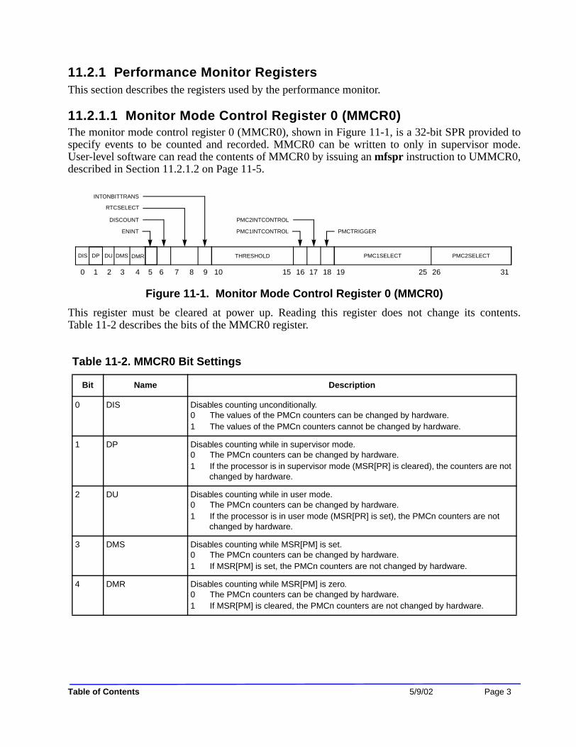
11.2.1 Performance Monitor RegistersThis section describes the registers used by the performance monitor.
11.2.1.1 Monitor Mode Control Register 0 (MMCR0)The monitor mode control register 0 (MMCR0), shown in Figure 11-1, is a 32-bit SPR provided tospecify events to be counted and recorded. MMCR0 can be written to only in supervisor mode.User-level software can read the contents of MMCR0 by issuing an mfspr instruction to UMMCR0,described in Section 11.2.1.2 on Page 11-5.
Figure 11-1. Monitor Mode Control Register 0 (MMCR0)
This register must be cleared at power up. Reading this register does not change its contents.Table 11-2 describes the bits of the MMCR0 register.
Table 11-2. MMCR0 Bit Settings
Bit Name Description
0 DIS Disables counting unconditionally. 0 The values of the PMCn counters can be changed by hardware. 1 The values of the PMCn counters cannot be changed by hardware.
1 DP Disables counting while in supervisor mode. 0 The PMCn counters can be changed by hardware.1 If the processor is in supervisor mode (MSR[PR] is cleared), the counters are not
changed by hardware.
2 DU Disables counting while in user mode. 0 The PMCn counters can be changed by hardware. 1 If the processor is in user mode (MSR[PR] is set), the PMCn counters are not
changed by hardware.
3 DMS Disables counting while MSR[PM] is set.0 The PMCn counters can be changed by hardware.1 If MSR[PM] is set, the PMCn counters are not changed by hardware.
4 DMR Disables counting while MSR[PM] is zero. 0 The PMCn counters can be changed by hardware.1 If MSR[PM] is cleared, the PMCn counters are not changed by hardware.
0 1 2 3 4 5 6 7 8 9 10 15 16 17 18 19 25 26 31
DMSDU THRESHOLD
INTONBITTRANS
DISCOUNT
PMC1SELECTDP PMC2SELECTDIS DMR
PMC1INTCONTROLENINT
PMC2INTCONTROL
RTCSELECT
PMCTRIGGER
Table of Contents 5/9/02 Page 3

MMCR0 can be accessed with the mtspr and mfspr instructions using SPR 952.
5 ENINT Enables performance monitor interrupt signaling.0 Interrupt signaling is disabled.1 Interrupt signaling is enabled.Cleared by hardware when a performance monitor interrupt is taken. To re-enable these interrupt signals, software must set this bit after servicing the performance monitor interrupt. The IPL ROM code clears this bit before passing control to the operating system.
6 DISCOUNT Disables counting of PMCn when a performance monitor interrupt is signaled (that is, ((PMCnINTCONTROL = 1) & (PMCn[0] = 1) & (ENINT = 1)) or the occurrence of an enabled time base transition with ((INTONBITTRANS =1) & (ENINT = 1)). 0 Signaling a performance monitor interrupt does not affect counting status of
PMCn.1 The signaling of a performance monitor interrupt prevents changing of PMC1
counter. The PMCn counter does not change if PMC2COUNTCTL = 0.Because a time base signal could have occurred along with an enabled counter overflow condition, software should always reset INTONBITTRANS to zero, if the value in INTONBITTRANS was a one.
7–8 RTCSELECT Time base lower (TBL) bit selection enable 00 Pick bit 31 to count01 Pick bit 23 to count10 Pick bit 19 to count11 Pick bit 15 to count
9 INTONBITTRANS Causes interrupt signaling on bit transition (identified in RTCSELECT) from off to on.0 Do not allow interrupt signal on the transition of a chosen bit.1 Signal interrupt on the transition of a chosen bit.Software is responsible for setting and clearing INTONBITTRANS.
10–15 THRESHOLD Threshold value. All 6 bits are supported by the 750CX; allowing threshold values from 0 to 63. The intent of the THRESHOLD support is to characterize L1 data cache misses.
16 PMC1INTCONTROL Enables interrupt signaling due to PMC1 counter overflow.0 Disable PMC1 interrupt signaling due to PMC1 counter overflow.1 Enable PMC1 Interrupt signaling due to PMC1 counter overflow.
17 PMCINTCONTROL Enable interrupt signaling due to any PMC2–PMC4 counter overflow. Overrides the setting of DISCOUNT. 0 Disable PMC2–PMC4 interrupt signaling due to PMC2–PMC4 counter overflow.1 Enable PMC2–PMC4 interrupt signaling due to PMC2–PMC4 counter overflow.
18 PMCTRIGGER Can be used to trigger counting of PMC2–PMC4 after PMC1 has overflowed or after a performance monitor interrupt is signaled.0 Enable PMC2–PMC4 counting. 1 Disable PMC2–PMC4 counting until either PMC1[0] = 1 or a performance monitor
interrupt is signaled.
19–25 PMC1SELECT PMC1 input selector, 128 events selectable; 25 defined. See Table 11-5.
26–31 PMC2SELECT PMC2 input selector, 64 events selectable; 21 defined. See Table 11-6.
Table 11-2. MMCR0 Bit Settings (Continued)
Bit Name Description
Page 4 Version 1.1 IBM PowerPC 750CX/750CXe RISC Microprocessor User’s Manual

11.2.1.2 User Monitor Mode Control Register 0 (UMMCR0)The contents of MMCR0 are reflected to UMMCR0, which can be read by user-level software.UMMCR0 can be accessed with the mfspr instructions using SPR 936.
11.2.1.3 Monitor Mode Control Register 1 (MMCR1)The monitor mode control register 1 (MMCR1) functions as an event selector for performancemonitor counter registers 3 and 4 (PMC3 and PMC4). The MMCR1 register is shown in Figure 11-2.
Figure 11-2. Monitor Mode Control Register 1 (MMCR1)
Bit settings for MMCR1 are shown in Table 11-3. The corresponding events are described inSection 11.2.1.5, "Performance Monitor Counter Registers (PMC1–PMC4)".
MMCR1 can be accessed with the mtspr and mfspr instructions using SPR 956. User-level softwarecan read the contents of MMCR1 by issuing an mfspr instruction to UMMCR1, described inSection 11.2.1.4, "User Monitor Mode Control Register 1 (UMMCR1)"
11.2.1.4 User Monitor Mode Control Register 1 (UMMCR1)The contents of MMCR1 are reflected to UMMCR1, which can be read by user-level software.UMMCR1 can be accessed with the mfspr instructions using SPR 940.
11.2.1.5 Performance Monitor Counter Registers (PMC1–PMC4)PMC1–PMC4, shown in Figure 11-3, are 32-bit counters that can be programmed to generateinterrupt signals when they overflow.
Figure 11-3. Performance Monitor Counter Registers (PMC1–PMC4)
Table 11-3. MMCR1 Bit Settings
Bits Name Description
0–4 PMC3SELECT PMC3 input selector. 32 events selectable. See Table 11-7 for defined selections.
5–9 PMC4SELECT PMC4 input selector. 32 events selectable. See Table 11-8 for defined selections.
10–31 — Reserved
0 4 5 9 10 31
Reserved
PMC3SELECT PMC4SELECT 0 0 þþ0 0 0 0 þþ0 0 0 0 þþ0 0 0 0 þþ0 0 0 0 þþ0 0 0 0 þþ
0 1 31
OV Counter Value
Tab
le of Contents 5/9/02 Page 5
The bits contained in the PMC registers are described in Table 11-4.
Counters overflow when the high-order bit (the sign bit) becomes set; that is, they reach the value2147483648 (0x8000_0000). However, an interrupt is not signaled unless both MMCR0[ENINT] andeither PMC1INTCONTROL or PMCINTCONTROL in the MMCR0 register are also set asappropriate.
NOTE: The interrupts can be masked by clearing MSR[EE]; the interrupt signal condition may occur with MSR[EE] cleared, but the exception is not taken until MSR[EE] is set. Setting MMCR0[DISCOUNT] forces counters to stop counting when a counter interrupt occurs.
Software is expected to use the mtspr instruction to explicitly set PMC to non-overflowed values.Setting an overflowed value may cause an erroneous exception. For example, if bothMMCR0[ENINT] and either PMC1INTCONTROL or PMCINTCONTROL are set and the mtsprinstruction loads an overflow value, an interrupt signal may be generated without an event countinghaving taken place.
The event to be monitored can be chosen by setting MMCR0[19–31]. The selected events are countedbeginning when MMCR0 is set until either MMCR0 is reset or a performance monitor interrupt isgenerated. Table 11-5 lists the selectable events and their encodings.
Table 11-4. PMCn Bit Settings
Bits Name Description
0 OV Overflow. When this bit is set, it indicates this counter has reached its maximum value.
1–31 Counter value Indicates the number of occurrences of the specified event.
Table 11-5. PMC1 Events—MMCR0[19–25] Select Encodings
Encoding Description
000 0000 Register holds current value.
000 0001 Number of processor cycles.
000 0010 Number of instructions that have completed. Does not include folded branches.
0000011 Number of transitions from 0 to 1 of specified bits in the time base lower (TBL) register. Bits are specified through RTCSELECT, MMCR0[7–8]. 00 = 31, 01 = 23, 10 = 19, 11 = 15
0000100 Number of instructions dispatched—0, 1, or 2 instructions per cycle.
0000101 Number of eieio instructions completed.
0000110 Number of cycles spent performing table search operations for the ITLB.
0000111 Number of accesses that hit the L2. This event includes cache ops (i.e., dcbz).
0001000 Number of valid instruction EAs delivered to the memory subsystem.
0001001 Number of times the address of an instruction being completed matches the address in the IABR.
0001010 Number of loads that miss the L1 with latencies that exceeded the threshold value.
0001011 Number of branches that are unresolved when processed.
0001100 Number of cycles the dispatcher stalls due to a second unresolved branch in the instruction stream.
All others Reserved. May be used in a later revision.
Page 6 Version 1.1 IBM PowerPC 750CX/750CXe RISC Microprocessor User’s Manual

Bits MMCR0[26–31] specify events associated with PMC2, as shown in Table 11-6.
Table 11-6. PMC2 Events—MMCR0[26–31] Select Encodings
Encoding Description
00 0000 Register holds current value.
00 0001 Counts processor cycle.
00 0010 Counts completed instructions. Does not include folded branches.
00 0011 Counts transitions from 0 to 1 of TBL bits specified through MMRC0[RTCSELECT], 00 = 47, 01 = 51, 10 = 55, 11 = 63
00 0100 Counts instructions dispatched: 0, 1, or 2 instructions per cycle.
00 0101 Counts L1 instruction cache misses.
00 0110 Counts ITLB misses.
00 0111 Counts L2 instruction misses.
00 1000 Counts branches predicted or resolved not taken.
00 1001 Counts MSR[PR] bit toggles.
00 1010 Counts times a reserved load operations completes.
00 1011 Counts completed load and store instructions.
00 1100 Counts snoops to the L1 and the L2.
001101 Counts the L1 castout to the L2.
001110 Counts completed system unit instructions.
001111 Counts instruction fetch misses in the L1.
010000 Counts branches allowing out-of-order execution that resolved correctly.
All others Reserved.
Table of Contents 5/9/02 Page 7

Bits MMCR1[0–4] specify events associated with PMC3, as shown in Table 11-7.
Table 11-7. PMC3 Events—MMCR1[0–4] Select Encodings
Encoding Description
0 0000 Register holds current value.
0 0001 Number of processor cycles.
0 0010 Number of completed instructions, not including folded branches.
0 0011 Number of transitions from 0 to 1 of specified bits in the time base lower (TBL) register. Bits are specified through RTCSELECT, MMCR0[7–8]. 00 = 31, 01 = 23, 10 = 19, 11 = 15
0 0100 Number of instructions dispatched. 0, 1, or 2 per cycle.
0 0101 Number of L1 data cache misses. Does not include cache ops.
0 0110 Number of DTLB misses.
0 0111 Number of L2 data misses.
0 1000 Number of predicted branches that were taken.
0 1001 Reserved.
0 1010 Number of store conditional instructions completed.
0 1011 Number of instructions completed from the FPU.
0 1100 Number of L2 castouts caused by snoops to modified lines.
0 1101 Number of cache operations that hit in the L2 cache.
0 1110 Reserved.
0 1111 Number of cycles generated by L1 load misses.
1 0000 Number of branches in the second speculative stream that resolve correctly.
1 0001 Number of cycles the BPU stalls due to LR or CR unresolved dependencies.
All others Reserved. May be used in a later revision.
Page 8 Version 1.1 IBM PowerPC 750CX/750CXe RISC Microprocessor User’s Manual

Bits MMCR1[5–9] specify events associated with PMC4, as shown in Table 11-8.
The PMC registers can be accessed with the mtspr and mfspr instructions using the following SPRnumbers:
• PMC1 is SPR 953
• PMC2 is SPR 954
• PMC3 is SPR 957
• PMC4 is SPR 958
11.2.1.6 User Performance Monitor Counter Registers (UPMC1–UPMC4)The contents of the PMC1–PMC4 are reflected to UPMC1–UPMC4, which can be read by user-levelsoftware. The UPMC registers can be read with the mfspr instructions using the following SPRnumbers:
• UPMC1 is SPR 937
• UPMC2 is SPR 938
• UPMC3 is SPR 941
Table 11-8. PMC4 Events—MMCR1[5–9] Select Encodings
Encoding Comments
00000 Register holds current value
00001 Number of processor cycles
00010 Number of completed instructions, not including folded branches
00011 Number of transitions from 0 to 1 of specified bits in the time base lower (TBL) register. Bits are specified through RTCSELECT, MMCR0[7–8]. 00 = 31, 01 = 23, 10 = 19, 11 = 15
00100 Number of instructions dispatched. 0, 1, or 2 per cycle
00101 Number of L2 castouts
00110 Number of cycles spent performing table searches for DTLB accesses.
00111 Reserved. May be used in a later revision.
01000 Number of mispredicted branches. Reserved for future use.
01001 Reserved. May be used in a later revision.
01010 Number of store conditional instructions completed with reservation intact
01011 Number of completed sync instructions
01100 Number of snoop request retries
01101 Number of completed integer operations
01110 Number of cycles the BPU cannot process new branches due to having two unresolved branches
All others Reserved. May be used in a later revision.
Table of Contents 5/9/02 Page 9

• UPMC4 is SPR 942
11.2.1.7 Sampled Instruction Address Register (SIA) The sampled instruction address register (SIA) is a supervisor-level register that contains the effectiveaddress of an instruction executing at or around the time that the processor signals the performancemonitor interrupt condition. The SIA is shown in Figure 11-4.
Figure 11-4. Sampled instruction Address Registers (SIA)
If the performance monitor interrupt is triggered by a threshold event, the SIA contains the addressof the exact instruction (called the sampled instruction) that caused the counter to overflow.
If the performance monitor interrupt was caused by something besides a threshold event, the SIAcontains the address of the last instruction completed during that cycle. SIA can be accessed with themtspr and mfspr instructions using SPR 955.
11.2.1.8 User Sampled Instruction Address Register (USIA) The contents of SIA are reflected to USIA, which can be read by user-level software. USIA can beaccessed with the mfspr instructions using SPR 939.
11.3 Event CountingCounting can be enabled if conditions in the processor state match a software-specified condition.Because a software task scheduler may switch a processor’s execution among multiple processes andbecause statistics on only a particular process may be of interest, a facility is provided to mark aprocess. The performance monitor (PM) bit, MSR[29] is used for this purpose. System software mayset this bit when a marked process is running. This enables statistics to be gathered only during theexecution of the marked process. The states of MSR[PR] and MSR[PM] together define a state thatthe processor (supervisor or program) and the process (marked or unmarked) may be in at any time.If this state matches a state specified by the MMCR, the state for which monitoring is enabled,counting is enabled.
The following are states that can be monitored:
• (Supervisor) only
• (User) only
• (Marked and user) only
• (Not marked and user) only
• (Marked and supervisor) only
• (Not marked and supervisor) only
• (Marked) only
• (Not marked) only
0 31
Instruction Address
Page 10 Version 1.1 IBM PowerPC 750CX/750CXe RISC Microprocessor User’s Manual

In addition, one of two unconditional counting modes may be specified:
• Counting is unconditionally enabled regardless of the states of MSR[PM] and MSR[PR]. This can be accomplished by clearing MMCR0[0–4].
• Counting is unconditionally disabled regardless of the states of MSR[PM] and MSR[PR]. This is done by setting MMCR0[0].
The performance monitor counters count specified events and are used to generate performancemonitor exceptions when an overflow (most-significant bit is a 1) situation occurs. The 750CXperformance monitor has four, 32-bit registers that can count up to 0x7FFFFFFF (2,147,483,648 indecimal) before overflowing. Bit 0 of the registers is used to determine when an interrupt conditionexists.
11.4 Event SelectionEvent selection is handled through MMCR0 and MMCR1, described in Table 11-2 on Page 11-3 andTable 11-3 on Page 11-5, respectively. Event selection is described as follows:
• The four event-select fields in MMCR0 and MMCR1 are as follows.
— MMCR0[19–25] PMC1SELECT—PMC1 input selector, 128 events selectable; 25 defined. See Table 11-5.
— MMCR0[26–31] PMC2SELECT—PMC2 input selector, 64 events selectable; 21 defined. See Table 11-6.
— MMCR0[0–4] PMC3SELECT—PMC3 input selector. 32 events selectable, defined. See Table 11-7.
— MMCR0[5–9] PMC4SELECT—PMC4 input selector. 32 events selectable. See Table 11-8.
• In the tables, a correlation is established between each counter, events to be traced, and the pattern required for the desired selection.
• The first five events are common to all four counters and are considered to be reference events. These are as follows.
— 00000—Register holds current value
— 00001—Number of processor cycles
— 00010—Number of completed instructions, not including folded branches
— 00011—Number of transitions from 0 to 1 of specified bits in the time base lower (TBL) register. Bits are specified through RTCSELECT, MMCR0[7–8]. 00 = 31, 01 = 23, 10 = 19, 11 = 15
— 00100—Number of instructions dispatched. 0, 1, or 2 per cycle
• Some events can have multiple occurrences per cycle, and therefore need two or three bits to represent them.
Table of Contents 5/9/02 Page 11

11.5 Notes The following warnings should be noted.
• Only those load and store in queue position 0 of their respective load/store queues are monitored when a threshold event is selected in PMC1.
• The 750CX cannot accurately track threshold events with respect to the following types of loads and stores.
— Unaligned load and store operations that cross a word boundary.
— Load and store multiple operations.
— Load and store string operations.
Page 12 Version 1.1 IBM PowerPC 750CX/750CXe RISC Microprocessor User’s Manual

Chapter 12 Instruction Set120
This chapter lists the PowerPC instruction set in alphabetical order by mnemonic. Note that each entryincludes the instruction formats and a quick reference ‘legend’ that provides such information as thelevel(s) of the PowerPC architecture in which the instruction may be found—user instruction setarchitecture (UISA), virtual environment architecture (VEA), and operating environment architecture(OEA); and the privilege level of the instruction—user or supervisor-level (an instruction is assumedto be user-level unless the legend specifies that it is supervisor-level); and the instruction formats. Theformat diagrams show, horizontally, all valid combinations of instruction fields; for a graphicalrepresentation of these instruction formats.
A description of the instruction fields and pseudocode conventions are also provided.
NOTE: The architecture specification refers to user-level and supervisor-level as problem state and privileged state, respectively.
12.1 Instruction Formats Instructions are four bytes long and word-aligned, so when instruction addresses are presented to theprocessor (as in branch instructions) the two low-order bits are ignored. Similarly, whenever theprocessor develops an instruction address, its two low-order bits are zero.
Bits 0–5 always specify the primary opcode. Many instructions also have an extended opcode. Theremaining bits of the instruction contain one or more fields for the different instruction formats.
Some instruction fields are reserved, or must contain a predefined value as shown in the individualinstruction layouts. If a reserved field does not have all bits cleared, or if a field that must contain aparticular value does not contain that value, the instruction form is invalid and the results aredescribed in Chapter 4, “Addressing Modes and Instruction Set Summary” in the PowerPCMicroprocessor Family: The Programming Environments manual.
Within the instruction format diagram the instruction operation code and extended operation code (ifextended form) are specified in decimal. These fields have been converted to hexadecimal and areshown on line two for each instruction definition.
12.1.1 Split-Field NotationSome instruction fields occupy more than one contiguous sequence of bits or occupy a contiguoussequence of bits used in permuted order. Such a field is called a split field. Split fields that representthe concatenation of the sequences from left to right are shown in lowercase letters. These splitfields— spr and tbr—are described in Table 12-1.
Table 12-1. Split-Field Notation and Conventions
Field Description
spr (11–20) This field is used to specify a special-purpose register for the mtspr and mfspr instructions. The encoding is described in Section 4.4.2.2, “Move to/from Special-Purpose Register Instructions (OEA)”, in the PowerPC Microprocessor Family: The Programming Environments manual.
tbr (11–20) This field is used to specify either the time base lower (TBL) or time base upper (TBU).
Table of Contents 5/9/02 Page 1

12.1.2 Instruction Fields Table 12-2 describes the instruction fields used in the various instruction formats.
Table 12-2. Instruction Syntax Conventions
Field Description
AA (30) Absolute address bit.0 The immediate field represents an address relative to the current instruction address (CIA). (For
more information on the CIA, see Table 12-3.) The effective (logical) address of the branch is either the sum of the LI field sign-extended to 32 bits and the address of the branch instruction or the sum of the BD field sign-extended to 32 bits and the address of the branch instruction.
1 The immediate field represents an absolute address. The effective address (EA) of the branch is the LI field sign-extended to 32 bits or the BD field sign-extended to 32 bits.
Note: The LI and BD fields are sign-extended to 32 bits.
BD (16–29) Immediate field specifying a 14-bit signed two's complement branch displacement that is concatenated on the right with 0b00 and sign-extended to 32 bits.
BI (11–15) This field is used to specify a bit in the CR to be used as the condition of a branch conditional instruction.
BO (6–10) This field is used to specify options for the branch conditional instructions. The encoding is described in Section 4.2.4.2, “Conditional Branch Control” in the PowerPC Microprocessor Family: The Programming Environments manual.
crbA (11–15) This field is used to specify a bit in the CR to be used as a source.
crbB (16–20) This field is used to specify a bit in the CR to be used as a source.
crbD (6–10) This field is used to specify a bit in the CR, or in the FPSCR, as the destination of the result of an instruction.
crfD (6–8) This field is used to specify one of the CR fields, or one of the FPSCR fields, as a destination.
crfS (11–13) This field is used to specify one of the CR fields, or one of the FPSCR fields, as a source.
CRM (12–19) This field mask is used to identify the CR fields that are to be updated by the mtcrf instruction.
d (16–31, or20-31)
Immediate field specifying a signed two's complement integer that is sign-extended to 32 bits.
FM (7–14) This field mask is used to identify the FPSCR fields that are to be updated by the mtfsf instruction.
frA (11–15) This field is used to specify an FPR as a source.
frB (16–20) This field is used to specify an FPR as a source.
frC (21–25) This field is used to specify an FPR as a source.
frD (6–10) This field is used to specify an FPR as the destination.
frS (6–10) This field is used to specify an FPR as a source.
IMM (16–19) Immediate field used as the data to be placed into a field in the FPSCR.
LI (6–29) Immediate field specifying a 24-bit signed two's complement integer that is concatenated on the right with 0b00 and sign-extended to 32 bits.
Page 2 Version 1.1 IBM PowerPC 750CX/750CXe RISC Microprocessor User’s Manual

LK (31) Link bit.0 Does not update the link register (LR).1 Updates the LR. If the instruction is a branch instruction, the address of the instruction following
the branch instruction is placed into the LR.
MB (21–25) and ME (26–30)
These fields are used in rotate instructions to specify a 32-bit mask in the PowerPC Microprocessor Family: The Programming Environments manual.
NB (16–20) This field is used to specify the number of bytes to move in an immediate string load or store.
OE (21) This field is used for extended arithmetic to enable setting OV and SO in the XER.
OPCD (0–5) Primary opcode field
rA (11–15) This field is used to specify a GPR to be used as a source or destination.
rB (16–20) This field is used to specify a GPR to be used as a source.
Rc (31) Record bit.0 Does not update the condition register (CR).1 Updates the CR to reflect the result of the operation.
For integer instructions, CR bits 0–2 are set to reflect the result as a signed quantity and CR bit 3 receives a copy of the summary overflow bit, XER[SO]. The result as an unsigned quantity or a bit string can be deduced from the EQ bit. For floating-point instructions, CR bits 4–7 are set to reflect floating-point exception, floating-point enabled exception, floating-point invalid operation exception, and floating-point overflow exception.
(Note that exceptions are referred to as interrupts in the architecture specification.)
rD (6–10) This field is used to specify a GPR to be used as a destination.
rS (6–10) This field is used to specify a GPR to be used as a source.
SH (16–20) This field is used to specify a shift amount.
SIMM (16–31) This immediate field is used to specify a 16-bit signed integer.
SR (12–15) This field is used to specify one of the 16 segment registers.
TO (6–10) This field is used to specify the conditions on which to trap. The encoding is described in Section 4.2.4.6, “Trap Instructions” in the PowerPC Microprocessor Family: The Programming Environments manual.
UIMM (16–31) This immediate field is used to specify a 16-bit unsigned integer.
XO (21–30, 22–30, 25-30 or 26–30)
Extended opcode field.
Table 12-2. Instruction Syntax Conventions (Continued)
Field Description
Table of Contents 5/9/02 Page 3

12.1.3 Notation and ConventionsThe operation of some instructions is described by a semiformal language (pseudocode). SeeTable 12-3 for a list of pseudocode notation and conventions used throughout this ¼¼³chapter.
Table 12-3. Notation and Conventions
Notation/Convention Meaning
← Assignment
←iea Assignment of an 32-bit instruction effective address.
¬ NOT logical operator
∗ Multiplication
÷ Division (yielding quotient)
+ Two’s-complement addition
– Two’s-complement subtraction, unary minus
=,≠ Equals and Not Equals relations
<,≤,≥, >, Signed comparison relations
. (period) Update. When used as a character of an instruction mnemonic, a period (.) means that the instruction updates the condition register field.
c Carry. When used as a character of an instruction mnemonic, a ‘c’ indicates a carry out in XER[CA].
e Extended Precision.When used as the last character of an instruction mnemonic, an ‘e’ indicates the use of XER[CA] as an operand in the instruction and records a carry out in XER[CA].
o Overflow. When used as a character of an instruction mnemonic, an ‘o’ indicates the record of an overflow in XER[OV] and CR0[SO] for integer instructions or CR1[SO] for floating-point instructions.
<U, >U Unsigned comparison relations
? Unordered comparison relation
&, | AND, OR logical operators
|| Used to describe the concatenation of two values (that is, 010 || 111 is the same as 010111)
⊕ , ≡ Exclusive-OR, Equivalence logical operators (for example, (a ≡ b) = (a ⊕ ¬ b))
0bnnnn A number expressed in binary format.
0xnnnn orx’nnnn nnnn’
A number expressed in hexadecimal format.
(n)x The replication of x, n times (that is, x concatenated to itself n – 1 times).(n)0 and (n)1 are special cases. A description of the special cases follows:
• (n)0 means a field of n bits with each bit equal to 0. Thus (5)0 is equivalent to 0b00000.
• (n)1 means a field of n bits with each bit equal to 1. Thus (5)1 is equivalent to0b11111.
Page 4 Version 1.1 IBM PowerPC 750CX/750CXe RISC Microprocessor User’s Manual

(rA|0) The contents of rA if the rA field has the value 1–31, or the value 0 if the rA field is 0.
(rX) The contents of rX
x[n] n is a bit or field within x, where x is a register
xn x is raised to the nth power
ABS(x) Absolute value of x
CEIL(x) Least integer x
Characterization Reference to the setting of status bits in a standard way that is explained in the text.
CIA Current instruction address.The 32-bit address of the instruction being described by a sequence of pseudocode. Used by relative branches to set the next instruction address (NIA) and by branch instructions with LK = 1 to set the link register. Does not correspond to any architected register.
Clear Clear the leftmost or rightmost n bits of a register to 0. This operation is used for rotate and shift instructions.
Clear left and shift left Clear the leftmost b bits of a register, then shift the register left by n bits. This operation can be used to scale a known non-negative array index by the width of an element. These operations are used for rotate and shift instructions.
Cleared Bits are set to 0.
Do Do loop.• Indenting shows range. • “To” and/or “by” clauses specify incrementing an iteration variable.• “While” clauses give termination conditions.
DOUBLE(x) Result of converting x from floating-point single-precision format to floating-point double-precision format.
Extract Select a field of n bits starting at bit position b in the source register, right or left justify this field in the target register, and clear all other bits of the target register to zero. This operation is used for rotate and shift instructions.
EXTS(x) Result of extending x on the left with sign bits
GPR(x) General-purpose register x
if...then...else... Conditional execution, indenting shows range, else is optional.
Insert Select a field of n bits in the source register, insert this field starting at bit position b of the target register, and leave other bits of the target register unchanged. (No simplified mnemonic is provided for insertion of a field when operating on double words; such an insertion requires more than one instruction.) This operation is used for rotate and shift instructions. (Note that simplified mnemonics are referred to as extended mnemonics in the architecture specification.)
Leave Leave innermost do loop, or the do loop described in leave statement.
MASK(x, y) Mask having ones in positions x through y (wrapping if x > y) and zeros elsewhere.
MEM(x, y) Contents of y bytes of memory starting at address x
Table 12-3. Notation and Conventions (Continued)
Notation/Convention Meaning
Table of Contents 5/9/02 Page 5

Table 12-4 describes instruction field notation conventions used throughout this chapter.
NIA Next instruction address, which is the32-bit address of the next instruction to be executed (the branch destination) after a successful branch. In pseudocode, a successful branch is indicated by assigning a value to NIA. For instructions which do not branch, the next instruction address is CIA + 4. Does not correspond to any architected register.
OEA PowerPC operating environment architecture
Rotate Rotate the contents of a register right or left n bits without masking. This operation is used for rotate and shift instructions.
reserved
ROTL(x, y) Result of rotating the value x left y positions, where x is 32 bits long
Set Bits are set to 1.
Shift Shift the contents of a register right or left n bits, clearing vacated bits (logical shift). This operation is used for rotate and shift instructions.
SINGLE(x) Result of converting x from floating-point double-precision format to floating-point single-precision format.
SPR(x) Special-purpose register x
TRAP Invoke the system trap handler.
Undefined An undefined value. The value may vary from one implementation to another, and from one execution to another on the same implementation.
UISA PowerPC user instruction set architecture
VEA PowerPC virtual environment architecture
Table 12-4. Instruction Field Conventions
The Architecture Specification
Equivalent to:
BA, BB, BT crbA, crbB, crbD (respectively)
BF, BFA crfD, crfS (respectively)
D d
DS ds
FLM FM
FRA, FRB, FRC, FRT, FRS frA, frB, frC, frD, frS (respectively)
FXM CRM
RA, RB, RT, RS rA, rB, rD, rS (respectively)
SI SIMM
Table 12-3. Notation and Conventions (Continued)
Notation/Convention Meaning
Page 6 Version 1.1 IBM PowerPC 750CX/750CXe RISC Microprocessor User’s Manual

Precedence rules for pseudocode operators are summarized in Table 12-5.
Operators higher in Table 12-5 are applied before those lower in the table. Operators at the same levelin the table associate from left to right, from right to left, or not at all, as shown. For example, “–”(unary minus) associates from left to right, so a – b – c = (a – b) – c. Parentheses are used to overridethe evaluation order implied by Table 12-5, or to increase clarity; parenthesized expressions areevaluated before serving as operands.Note that the all pseudocode examples provided in this chapterare for 32-bit implementations.PowerPC Instruction Set
12.1.4 Computation ModesThe PowerPC architecture is defined for 32-bit implementations, in which all registers except theFPRs are 32 bits long, and effective addresses are 32 bits long. The FPR registers are 64 bits long. Formore information on computation modes see Section 4.1.1, “Computation Modes,” in the PowerPCMicroprocessor Family: The Programming Environments manual.
U IMM
UI UIMM
/, //, /// 0...0 (shaded)
Table 12-5. Precedence Rules
Operators Associativity
x[n], function evaluation Left to right
(n)x or replication, x(n) or exponentiation
Right to left
unary –, ¬ Right to left
∗ , ÷ Left to right
+, – Left to right
|| Left to right
=, ≠,≤, <, >, ≥, <U, >U, ? Left to right
&, ⊕ , ≡ Left to right
| Left to right
– (range) None
←, ←iea None
Table 12-4. Instruction Field Conventions (Continued)
The Architecture Specification
Equivalent to:
Table of Contents 5/9/02 Page 7

12.2 PowerPC Instruction SetThe remainder of this chapter lists and describes the instruction set for the PowerPC architecture. Theinstructions are listed in alphabetical order by mnemonic. Figure 12-1 shows the format for eachinstruction description page.
Instruction Description
NOTE: The execution unit that executes the instruction may not be the same for all PowerPC processors.
addx addxAdd (x’7C00 0214’)
add rD,rA,rB (OE = 0 Rc = 0)add. rD,rA,rB (OE = 0 Rc = 1) addo rD,rA,rB (OE = 1 Rc = 0) addo. rD,rA,rB (OE = 1 Rc = 1)
rD ← (rA) + (rB)
The sum (rA) + (rB) is placed into rD.
Other registers altered:•Condition Register (CR0 field):Affected: LT, GT, EQ, SO (If Rc = 1)•XER:Affected: SO, OV (If OE = 1)
B OE266 Rc0 5 6 1011151620 21 22 30 31
31 D A
Instruction name
name (Instruction operation codes in hexadecimal)
Instruction syntax
Instruction encoding
Pseudocode description of instruction operation
Text description ofinstruction operation
Registers altered by instruction
Quick reference legendPowerPC Architecture Level Supervisor Level PowerPC Optional Form
UISA XO
Page 8 Version 1.1
IBM PowerPC 750 CX/750CXe RISC Microprocessor User’s Manual
addx addxAdd (x’7C00 0214’)
add rD,rA,rB (OE = 0 Rc = 0)add. rD,rA,rB (OE = 0 Rc = 1) addo rD,rA,rB (OE = 1 Rc = 0) addo. rD,rA,rB (OE = 1 Rc = 1)
rD ← (rA) + (rB)
The sum (rA) + (rB) is placed into rD.
The add instruction is preferred for addition because it sets few status bits.
Other registers altered:
• Condition Register (CR0 field):
Affected: LT, GT, EQ, SO (if Rc = 1)
NOTE: CR0 field may not reflect the infinitely precise result if overflow occurs (see XER below).
• XER:
Affected: SO, OV (if OE = 1)
NOTE: For more information on condition codes see Section 2.1.3, “Condition Register,” in the PowerPC Microprocessor Family: The Programming Environments manual and Section 2.1.5, “XER Register,” in the PowerPC Microprocessor Family: The Programming Environments manual.
0 5 6 10 11 15 16 20 21 22 30 31
31 D A B OE 266 Rc
PowerPC Architecture Level Supervisor Level PowerPC Optional Form
UISA XO
T
able of Contents 5/9/02 Page 9
addcx addcxAdd Carrying (x’7C00 0014’)
addc rD,rA,rB (OE = 0 Rc = 0)addc. rD,rA,rB (OE = 0 Rc = 1)addco rD,rA,rB (OE = 1 Rc = 0)addco. rD,rA,rB (OE = 1 Rc = 1)
rD ← (rA) + (rB)
The sum (rA) + (rB) is placed into rD.
Other registers altered:
• Condition Register (CR0 field)
Affected: LT, GT, EQ, SO (if Rc = 1)
NOTE: CR0 field may not reflect the infinitely precise result if overflow occurs (see XER below).
• XER
Affected: CA
Affected: SO, OV (if OE = 1)
NOTE: For more information on condition codes see Section 2.1.3, “Condition Register,” and Section 2.1.5, “XER Register,” in the PowerPC Microprocessor Family: The Programming Environments manual.
0 5 6 10 11 15 16 20 21 22 30 31
31 D A B OE 10 Rc
PowerPC Architecture Level Supervisor Level PowerPC Optional Form
UISA XO
P
age 10 Version 1.1 IBM PowerPC 750CX/750CXe RISC Microprocessor User’s Manual
addex addexAdd Extended (x’7C00 0114’)
adde rD,rA,rB (OE = 0 Rc = 0) adde. rD,rA,rB (OE = 0 Rc = 1) addeo rD,rA,rB (OE = 1 Rc = 0) addeo. rD,rA,rB (OE = 1 Rc = 1)
rD ← (rA) + (rB) + XER[CA]
The sum (rA) + (rB) + XER[CA] is placed into rD.
Other registers altered:
• Condition Register (CR0 field)
Affected: LT, GT, EQ, SO (if Rc = 1)
NOTE: CR0 field may not reflect the infinitely precise result if overflow occurs (see XER below).
• XER
Affected: CA
Affected: SO, OV (if OE = 1)
NOTE: For more information on condition codes see Section 2.1.3, “Condition Register,” and Section 2.1.5, “XER Register,” in the PowerPC Microprocessor Family: The Programming Environments manual.
0 5 6 10 11 15 16 20 21 22 30 31
31 D A B OE 138 Rc
PowerPC Architecture Level Supervisor Level PowerPC Optional Form
UISA XO
T
able of Contents 5/9/02 Page 11
addi addiAdd Immediate (x’3800 0000’)
addi rD,rA,SIMM
if rA = 0 then rD ← EXTS(SIMM)else rD ← (rA) + EXTS(SIMM)
The sum (rA|0) + sign extended SIMM is placed into rD.
The addi instruction is preferred for addition because it sets few status bits. Note that addi uses thevalue 0, not the contents of GPR0, if rA = 0.
Other registers altered:
• None
0 5 6 10 11 15 16 31
14 D A SIMM
PowerPC Architecture Level Supervisor Level PowerPC Optional Form
UISA D
P
age 12 Version 1.1 IBM PowerPC 750CX/750CXe RISC Microprocessor User’s Manual
addic addicAdd Immediate Carrying (x’3000 0000’)
addic rD,rA,SIMM
rD ← (rA) + EXTS(SIMM)
The sum (rA) + sign extended SIMM is placed into rD.
Other registers altered:
• XER:
NOTE: Affected: CAFor more information see Section 2.1.5, “XER Register,” in the PowerPC Microprocessor Family: The Programming Environments manual.
Simplified mnemonics:
subicrD,rA,value equivalent to addic rD,rA,–value
0 5 6 10 11 15 16 31
12 D A SIMM
PowerPC Architecture Level Supervisor Level PowerPC Optional Form
UISA D
T
able of Contents 5/9/02 Page 13
addic. addic.Add Immediate Carrying and Record (x’3400 0000’)
addic. rD,rA,SIMM
rD ← (rA) + EXTS(SIMM)
The sum (rA) + the sign extended SIMM is placed into rD.
Other registers altered:
• Condition Register (CR0 field)
Affected: LT, GT, EQ, SO
NOTE: CR0 field may not reflect the infinitely precise result if overflow occurs (see XER below).
• XER
Affected: CA
NOTE: For more information on condition codes see Section 2.1.3, “Condition Register,” and Section 2.1.5, “XER Register,” in the PowerPC Microprocessor Family: The Programming Environments manual.
Simplified mnemonics:
subic.rD,rA,value equivalent toaddic. rD,rA,–value
0 5 6 10 11 15 16 31
13 D A SIMM
PowerPC Architecture Level Supervisor Level PowerPC Optional Form
UISA D
P
age 14 Version 1.1 IBM PowerPC 750CX/750CXe RISC Microprocessor User’s Manual
addis addis Add Immediate Shifted (x’3C00 0000’)
addis rD,rA,SIMM
if rA = 0 then rD ← (SIMM || (16)0)else rD ← (rA) + (SIMM || (16)0)
The sum (rA|0) + (SIMM || 0x0000) is placed into rD.
The addis instruction is preferred for addition because it sets few status bits. Note that addis uses thevalue 0, not the contents of GPR0, if rA = 0.
Other registers altered:
• None
Simplified mnemonics:
lis rD, value equivalent toaddis rD,0,valuesubisrD,rA, value equivalent toaddis rD,rA,–value
0 5 6 10 11 15 16 31
15 D A SIMM
PowerPC Architecture Level Supervisor Level PowerPC Optional Form
UISA D
T
able of Contents 5/9/02 Page 15
addmex addmexAdd to Minus One Extended (x’7C00 01D4’)
addme rD,rA (OE = 0 Rc = 0)addme. rD,rA (OE = 0 Rc = 1)addmeo rD,rA (OE = 1 Rc = 0)addmeo. rD,rA (OE = 1 Rc = 1)
rD ← (rA) + XER[CA] – 1
The sum (rA) + XER[CA] + 0xFFFF_FFFF is placed into rD.
Other registers altered:
• Condition Register (CR0 field)
Affected: LT, GT, EQ, SO (if Rc = 1)
NOTE: CR0 field may not reflect the infinitely precise result if overflow occurs (see XER below).
• XER
Affected: CA
Affected: SO, OV (if OE = 1)
NOTE: For more information on condition codes see Section 2.1.3, “Condition Register,” and Section 2.1.5, “XER Register,” in the PowerPC Microprocessor Family: The Programming Environments manual.
0 5 6 10 11 15 16 20 21 22 30 31
Reserved
31 D A 0 0 0 0 0 OE 234 Rc
PowerPC Architecture Level Supervisor Level PowerPC Optional Form
UISA XO
P
age 16 Version 1.1 IBM PowerPC 750CX/750CXe RISC Microprocessor U ser’s Manual
addzex addzexAdd to Zero Extended (x’7C00 0194’)
addze rD,rA (OE = 0 Rc = 0)addze. rD,rA (OE = 0 Rc = 1)addzeo rD,rA (OE = 1 Rc = 0)addzeo. rD,rA (OE = 1 Rc = 1)
rD ← (rA) + XER[CA]
The sum (rA) + XER[CA] is placed into rD.
Other registers altered:
• Condition Register (CR0 field)
Affected: LT, GT, EQ, SO (if Rc = 1)
NOTE: CR0 field may not reflect the infinitely precise result if overflow occurs (see XER below).
• XER
Affected: CA
Affected: SO, OV (if OE = 1)
NOTE: For more information on condition codes see Section 2.1.3, “Condition Register,” and Section 2.1.5, “XER Register,” in the PowerPC Microprocessor Family: The Programming Environments manual.
0 5 6 10 11 15 16 20 21 22 30 31
Reserved
31 D A 0 0 0 0 0 OE 202 Rc
PowerPC Architecture Level Supervisor Level PowerPC Optional Form
UISA XO
T
able of Contents 5/9/02 Page 17
andx andxAND (x’7C00 0038’)
and rA,rS,rB (Rc = 0)and. rA,rS,rB (Rc = 1)
rA ← (rS) & (rB)
The contents of rS are ANDed with the contents of rB and the result is placed into rA.
Other registers altered:
• Condition Register (CR0 field)
Affected: LT, GT, EQ, SO (if Rc = 1)
0 5 6 10 11 15 16 20 21 30 31
31 S A B 28 Rc
PowerPC Architecture Level Supervisor Level PowerPC Optional Form
UISA X
P
age 18 Version 1.1 IBM PowerPC 750CX/750CXe RISC Microprocessor User’s Manual
andcx andcxAND with Complement (x’7C00 0078’)
andc rA,rS,rB (Rc = 0)andc. rA,rS,rB (Rc = 1)
rA ← (rS) & ¬ (rB)
The contents of rS are ANDed with the one’s complement of the contents of rB and the result isplaced into rA.
Other registers altered:
• Condition Register (CR0 field)
Affected: LT, GT, EQ, SO (if Rc = 1)
0 5 6 10 11 15 16 20 21 30 31
31 S A B 60 Rc
PowerPC Architecture Level Supervisor Level PowerPC Optional Form
UISA X
T
able of Contents 5/9/02 Page 19
andi. andi.AND Immediate (x’7000 0000’)
andi. rA,rS,UIMM
rA ← (rS) & ((16)0 || UIMM)
The contents of rS are ANDed with 0x000 || UIMM and the result is placed into rA.
Other registers altered:
• Condition Register (CR0 field)
Affected: LT, GT, EQ, SO
0 5 6 10 11 15 16 31
28 S A UIMM
PowerPC Architecture Level Supervisor Level PowerPC Optional Form
UISA D
P
age 20 Version 1.1 IBM PowerPC 750CX/750CXe RISC Microprocessor User’s Manual
andis. andis. AND Immediate Shifted (x’7400 0000’)
andis. rA,rS,UIMM
rA ← (rS) & (UIMM || (16)0)
The contents of rS are ANDed with UIMM || 0x0000 and the result is placed into rA.
Other registers altered:
• Condition Register (CR0 field)
Affected: LT, GT, EQ, SO
0 5 6 10 11 15 16 31
29 S A UIMM
PowerPC Architecture Level Supervisor Level PowerPC Optional Form
UISA D
T
able of Contents 5/9/02 Page 21
bx bxBranch (x’4800 0000’)
b target_addr (AA = 0 LK = 0)ba target_addr (AA = 1 LK = 0)bl target_addr (AA = 0 LK = 1)bla target_addr (AA = 1 LK = 1)
if AA = 1then NIA ←iea EXTS(LI || 0b00)else NIA ←iea CIA + EXTS(LI || 0b00)
if LK = 1then LR ←iea CIA + 4
target_addr specifies the branch target address.
If AA = 1, then the branch target address is the value LI || 0b00 sign-extended.
If AA = 0, then the branch target address is the sum of LI || 0b00 sign-extended plus the address ofthis instruction.
If LK = 1, then the effective address of the instruction following the branch instruction is placed intothe link register.
Other registers altered:
• Link Register (LR) (if LK = 1)
0 5 6 29 30 31
18 LI AA LK
PowerPC Architecture Level Supervisor Level PowerPC Optional Form
UISA I
P
age 22 Version 1.1 IBM PowerPC 750CX/750CXe RISC Microprocessor User’s Manual
bcx bcxBranch Conditional (x’4000 0000’)
bc BO,BI,target_addr (AA = 0 LK = 0)bca BO,BI,target_addr (AA = 1 LK = 0)bcl BO,BI,target_addr (AA = 0 LK = 1)bcla BO,BI,target_addr (AA = 1 LK = 1)
if ¬ BO[2] then CTR ← CTR – 1
ctr_ok ← BO[2] | ((CTR ≠ 0) ⊕ BO[3])cond_ok ← BO[0] | (CR[BI] ≡ BO[1])if ctr_ok & cond_ok
thenif AA = 1
then NIA ←iea EXTS(BD || 0b00)else NIA ←iea CIA + EXTS(BD || 0b00)
if LK then LR ←iea CIA + 4
target_addr specifies the branch target address.
The BI field specifies the bit in the condition register (CR) to be used as the condition of the branch.The BO field is encoded as described in Table 12-6.
Additional information about BO field encoding is provided in Section 4.2.4.2, “Conditional BranchControl,” in the PowerPC Microprocessor Family: The Programming Environments manual.
NOTE: In this table, z indicates a bit that is ignored. The z bits should be cleared, as they may be assigned a meaning in some future version of the PowerPC architecture.The y bit provides a hint about whether a conditional branch is likely to be taken, and may be used by some PowerPC implementations to improve performance.
Table 12-6. BO Operand Encodings
BO Description
0000y Decrement the CTR, then branch if the decremented CTR ¦ 0 and the condition is FALSE.
0001y Decrement the CTR, then branch if the decremented CTR = 0 and the condition is FALSE.
001zy Branch if the condition is FALSE.
0100y Decrement the CTR, then branch if the decremented CTR ¦ 0 and the condition is TRUE.
0101y Decrement the CTR, then branch if the decremented CTR = 0 and the condition is TRUE.
011zy Branch if the condition is TRUE.
1z00y Decrement the CTR, then branch if the decremented CTR ¦ 0.
1z01y Decrement the CTR, then branch if the decremented CTR = 0.
1z1zz Branch always.
0 5 6 10 11 15 16 29 30 31
16 BO BI BD AA LK
T
able of Contents 5/9/02 Page 23
If AA = 0, the branch target address is the sum of BD || 0b00 sign-extended and the address of thisinstruction.
If AA = 1, the branch target address is the value BD || 0b00 sign-extended.
If LK = 1, the effective address of the instruction following the branch instruction is placed into thelink register.
Other registers altered:
Affected: Count Register (CTR) (if BO[2] = 0)
Affected: Link Register (LR) (if LK = 1)
Simplified mnemonics:
blt target equivalent to bc 12,0,targetbne cr2,target equivalent tobc 4,10,targetbdnz target equivalent tobc 16,0,target
PowerPC Architecture Level Supervisor Level PowerPC Optional Form
UISA D
P
age 24 Version 1.1 IBM PowerPC 750CX/750CXe RISC Microprocessor User’s Manual
bcctrx bcctrxBranch Conditional to Count Register (x’4C00 0420’)
bcctr BO,BI (LK = 0)bcctrl BO,BI (LK = 1)
cond_ok ← BO[0] | (CR[BI] ≡ BO[1])if cond_ok
thenNIA ←iea CTR || 0b00if LK then LR ←iea CIA + 4
The BI field specifies the bit in the condition register to be used as the condition of the branch. TheBO field is encoded as described in Table 12-7. Additional information about BO field encoding isprovided in Section 4.2.4.2, “Conditional Branch Control,” in the PowerPC Microprocessor Family:The Programming Environments manual.
Table 12-7. BO Operand Encodings
The branch target address is CTR[0–29] || 0b00.
BO Description
0000y Decrement the CTR, then branch if the decremented CTR ¦ 0 and the condition is FALSE.
0001y Decrement the CTR, then branch if the decremented CTR = 0 and the condition is FALSE.
001zy Branch if the condition is FALSE.
0100y Decrement the CTR, then branch if the decremented CTR ¦ 0 and the condition is TRUE.
0101y Decrement the CTR, then branch if the decremented CTR = 0 and the condition is TRUE.
011zy Branch if the condition is TRUE.
1z00y Decrement the CTR, then branch if the decremented CTR ¦ 0.
1z01y Decrement the CTR, then branch if the decremented CTR = 0.
1z1zz Branch always.
In this table, z indicates a bit that is ignored. Note that the z bits should be cleared, as they may be assigned a meaning in some future version of the PowerPC architecture.
The y bit provides a hint about whether a conditional branch is likely to be taken, and may be used by some PowerPC implementations to improve performance.
0 5 6 10 11 15 16 20 21 30 31
Reserved
19 BO BI 0 0 0 0 0 528 LK
T
able of Contents 5/9/02 Page 25
If LK = 1, the effective address of the instruction following the branch instruction is placed into thelink register.
If the “decrement and test CTR” option is specified (BO[2] = 0), the instruction form is invalid.
Other registers altered:
• Link Register (LR) (if LK = 1)
Simplified mnemonics:
bltctr equivalent to bcctr 12,0bnectrcr2 equivalent to bcctr 4,10
PowerPC Architecture Level Supervisor Level PowerPC Optional Form
UISA XL
P
age 26 Version 1.1 IBM PowerPC 750CX/750CXe RISC Microprocessor User’s Manual
bclrx bclrxBranch Conditional to Link Register (x’4C00 0020’)
bclr BO,BI (LK = 0)bclrl BO,BI (LK = 1)
if ¬ BO[2] then CTR ← CTR – 1
ctr_ok ← BO[2] | ((CTR ≠ ¦ 0) ⊕ BO[3])cond_ok ← BO[0] | (CR[BI] ≡ BO[1])if ctr_ok & cond_ok
thenNIA ←iea LR[0–29] || 0b00if LK then LR ←iea CIA + 4
The BI field specifies the bit in the condition register to be used as the condition of the branch. TheBO field is encoded as described in Table 12-8. Additional information about BO field encoding isprovided in Section 4.2.4.2, “Conditional Branch Control,” in the PowerPC Microprocessor Family:The Programming Environments manual.
Table 12-8. BO Operand Encodings
BO Description
0000y Decrement the CTR, then branch if the decremented CTR ¦ 0 and the condition is FALSE.
0001y Decrement the CTR, then branch if the decremented CTR = 0 and the condition is FALSE.
001zy Branch if the condition is FALSE.
0100y Decrement the CTR, then branch if the decremented CTR¦ 0 and the condition is TRUE.
0101y Decrement the CTR, then branch if the decremented CTR = 0 and the condition is TRUE.
011zy Branch if the condition is TRUE.
1z00y Decrement the CTR, then branch if the decremented CTR ¦ 0.
1z01y Decrement the CTR, then branch if the decremented CTR = 0.
1z1zz Branch always.
If the BO field specifies that the CTR is to be decremented, the entire 32-bit CTR is decremented.
In this table, z indicates a bit that is ignored. Note that the z bits should be cleared, as they may be assigned a meaning in some future version of the PowerPC architecture.
The y bit provides a hint about whether a conditional branch is likely to be taken, and may be used by some PowerPC implementations to improve performance.
0 5 6 10 11 15 16 20 21 30 31
Reserved
19 BO BI 0 0 0 0 0 16 LK
T
able of Contents 5/9/02 Page 27
The branch target address is LR[0–29] || 0b00.
If LK = 1, then the effective address of the instruction following the branch instruction is placed intothe link register.
Other registers altered:
• Count Register (CTR) (if BO[2] = 0)
• Link Register (LR) (if LK = 1)
Simplified mnemonics:
bltlr equivalent to bclr 12,0bnelr cr2 equivalent to bclr 4,10 bdnzlr equivalent tobclr 16,0
PowerPC Architecture Level Supervisor Level PowerPC Optional Form
UISA XL
P
age 28 Version 1.1 IBM PowerPC 750CX/750CXe RISC Microprocessor User’s Manual
cmp cmp Compare (x’7C00 0000’)
cmp crfD,L,rA,rB
a ← (rA)b ← (rB)if a < b
then c ← 0b100else if a > b
then c ← 0b010else c ← 0b001
CR[(4 ∗ crfD)–(4 ∗ crfD + 3)] ← c || XER[SO]
The contents of rA are compared with the contents of rB, treating the operands as signed integers.The result of the comparison is placed into CR field crfD.
If L = 1 the instruction form is invalid.
Other registers altered:
• Condition Register (CR field specified by operand crfD)
Affected: LT, GT, EQ, SO
Simplified mnemonics:
cmpdrA,rB equivalent to cmp 0,1,rA,rBcmpwcr3,rA,rB equivalent to cmp 3,0,rA,rB
0 5 6 8 9 10 11 15 16 20 21 30 31
Reserved
B 0 0 0 0 0 0 0 0 0 0 031 crfD 0 L A
PowerPC Architecture Level Supervisor Level PowerPC Optional Form
UISA X
T
able of Contents 5/9/02 Page 29
cmpi cmpiCompare Immediate (x’2C00 0000’)
cmpi crfD,L,rA,SIMM
a ← (rA)if a < EXTS(SIMM)
then c ← 0b100else if a > EXTS(SIMM)
then c ← 0b010else c ← 0b001
CR[(4 ∗ crfD)–(4 ∗ crfD + 3)] ← c || XER[SO]
The contents of rA are compared with the sign-extended value of the SIMM field, treating theoperands as signed integers. The result of the comparison is placed into CR field crfD.
If L = 1 the instruction form is invalid.
Other registers altered:
• Condition Register (CR field specified by operand crfD)
Affected: LT, GT, EQ, SO
Simplified mnemonics:
cmpdirA,value equivalent tocmpi 0,1,rA,valuecmpwi cr3,rA,value equivalent tocmpi 3,0,rA,value
0 5 6 8 9 10 11 15 16 31
Reserved
SIMM11 crfD 0 L A
PowerPC Architecture Level Supervisor Level PowerPC Optional Form
UISA D
P
age 30 Version 1.1 IBM PowerPC 750CX/750CXe RISC Microprocessor U ser’s Manual
cmpl cmplCompare Logical (x’7C00 0040’)
cmpl crfD,L,rA,rB
a ← (rA)b ← (rB)if a <U b
then c ← 0b100else if a >U b
then c ← 0b010else c ← 0b001
CR[(4 ∗ crfD)–(4 ∗ crfD + 3)] ← c || XER[SO]
The contents of rA are compared with the contents of rB, treating the operands as unsigned integers.The result of the comparison is placed into CR field crfD.
If L = 1 the instruction form is invalid.
Other registers altered:
• Condition Register (CR field specified by operand crfD)
Affected: LT, GT, EQ, SO
Simplified mnemonics:
cmpldrA,rB equivalent tocmpl 0,1,rA,rBcmplw cr3,rA,rB equivalent tocmpl 3,0,rA,rB
0 5 6 8 9 10 11 15 16 20 21 31
Reserved
31 crfD 0 L A B 32 0
PowerPC Architecture Level Supervisor Level PowerPC Optional Form
UISA X
T
able of Contents 5/9/02 Page 31
cmpli cmpli Compare Logical Immediate (x’2800 0000’)
cmpli crfD,L,rA,UIMM
a ← (rA)if a <U ((16)0 || UIMM)
then c ← 0b100else if a >U ((16)0 || UIMM)
then c ← 0b010else c ← 0b001
CR[(4 ∗ crfD)-(4 ∗ crfD + 3)] ← c || XER[SO]
The contents of rA are compared with 0x0000 || UIMM, treating the operands as unsigned integers.The result of the comparison is placed into CR field crfD.
If L = 1 the instruction form is invalid.
Other registers altered:
• Condition Register (CR field specified by operand crfD)
Affected: LT, GT, EQ, SO
Simplified mnemonics:
cmpldir A,value equivalent tocmpli 0,1,rA,valuecmplwi cr3,rA,value equivalent tocmpli 3,0,rA,value
0 5 6 8 9 10 11 15 16 31
Reserved
UIMM10 crfD 0 L A
PowerPC Architecture Level Supervisor Level PowerPC Optional Form
UISA D
P
age 32 Version 1.1 IBM PowerPC 750CX/750CXe RISC Microprocessor U ser’s Manual
cntlzwx cntlzwxCount Leading Zeros Word (x’7C00 0034’)
cntlzw rA,rS (Rc = 0)cntlzw. rA,rS (Rc = 1)
n ← 0do while n < 32
if rS[n] = 1 then leaven ← n + 1
rA ← n
A count of the number of consecutive zero bits starting at bit 0 of rS is placed into rA. This numberranges from 0 to 32, inclusive.
Other registers altered:
• Condition Register (CR0 field)
Affected: LT, GT, EQ, SO (if Rc = 1)
NOTE: If Rc = 1, then LT is cleared in the CR0 field.
0 5 6 10 11 15 16 20 21 30 31
Reserved
31 S A 0 0 0 0 0 26 Rc
PowerPC Architecture Level Supervisor Level PowerPC Optional Form
UISA X
T
able of Contents 5/9/02 Page 33
crand crandCondition Register AND (x’4C00 0202’)
crand crbD,crbA,crbB
CR[crbD] ← CR[crbA] & CR[crbB]
The bit in the condition register specified by crbA is ANDed with the bit in the condition registerspecified by crbB. The result is placed into the condition register bit specified by crbD.
Other registers altered:
• Condition Register
Affected: Bit specified by operand crbD
0 5 6 10 11 15 16 20 21 30 31
Reserved
19 crbD crbA crbB 257 0
PowerPC Architecture Level Supervisor Level PowerPC Optional Form
UISA XL
P
age 34 Version 1.1 IBM PowerPC 750CX/750CXe RISC Microprocessor U ser’s Manual
crandc crandcCondition Register AND with Complement (x’4C00 0102’)
crandc crbD,crbA,crbB
CR[crbD] ← CR[crbA] & ¬ CR[crbB]
The bit in the condition register specified by crbA is ANDed with the complement of the bit in thecondition register specified by crbB and the result is placed into the condition register bit specifiedby crbD.
Other registers altered:
• Condition Register
Affected: Bit specified by operand crbD
0 5 6 10 11 15 16 20 21 30 31
Reserved
19 crbD crbA crbB 129 0
PowerPC Architecture Level Supervisor Level PowerPC Optional Form
UISA XL
T
able of Contents 5/9/02 Page 35
creqv creqvCondition Register Equivalent (x’4C00 0242’)
creqv crbD,crbA,crbB
CR[crbD] ← CR[crbA] ≡ CR[crbB]
The bit in the condition register specified by crbA is XORed with the bit in the condition registerspecified by crbB and the complemented result is placed into the condition register bit specified bycrbD.
Other registers altered:
• Condition Register
Affected: Bit specified by operand crbD
Simplified mnemonics:
crse crbD equivalent tocreqv crbD,crbD,crbD
0 5 6 10 11 15 16 20 21 30 31
Reserved
19 crbD crbA crbB 289 0
PowerPC Architecture Level Supervisor Level PowerPC Optional Form
UISA XL
P
age 36 Version 1.1 IBM PowerPC 750CX/750CXe RISC Microprocessor U ser’s Manual
crnand crnandCondition Register NAND (x’4C00 01C2’)
crnand crbD,crbA,crbB
CR[crbD] ← ¬ (CR[crbA] & CR[crbB])
The bit in the condition register specified by crbA is ANDed with the bit in the condition registerspecified by crbB and the complemented result is placed into the condition register bit specified bycrbD.
Other registers altered:
• Condition Register
Affected: Bit specified by operand crbD
0 5 6 10 11 15 16 20 21 30 31
Reserved
19 crbD crbA crbB 225 0
PowerPC Architecture Level Supervisor Level PowerPC Optional Form
UISA XL
T
able of Contents 5/9/02 Page 37
crnor crnorCondition Register NOR (x’4C00 0042’)
crnor crbD,crbA,crbB
CR[crbD] ← ¬ (CR[crbA] | CR[crbB])
The bit in the condition register specified by crbA is ORed with the bit in the condition registerspecified by crbB and the complemented result is placed into the condition register bit specified bycrbD.
Other registers altered:
• Condition Register
Affected: Bit specified by operand crbD
Simplified mnemonics:
crnot crbD,crbA equivalent to crnor crbD,crbA,crbA
0 5 6 10 11 15 16 20 21 30 31
Reserved
19 crbD crbA crbB 33 0
PowerPC Architecture Level Supervisor Level PowerPC Optional Form
UISA XL
P
age 38 Version 1.1 IBM PowerPC 750CX/750CXe RISC Microprocessor U ser’s Manual
cror crorCondition Register OR (x’4C00 0382’)
cror crbD,crbA,crbB
CR[crbD] ← CR[crbA] | CR[crbB]
The bit in the condition register specified by crbA is ORed with the bit in the condition registerspecified by crbB. The result is placed into the condition register bit specified by crbD.
Other registers altered:
• Condition Register
Affected: Bit specified by operand crbD
Simplified mnemonics:
crmove crbD,crbA equivalent tocror crbD,crbA,crbA
0 5 6 10 11 15 16 20 21 30 31
Reserved
19 crbD crbA crbB 449 0
PowerPC Architecture Level Supervisor Level PowerPC Optional Form
UISA XL
T
able of Contents 5/9/02 Page 39
crorc crorcCondition Register OR with Complement (x’4C00 0342’)
crorc crbD,crbA,crbB
CR[crbD] ← CR[crbA] | ¬ CR[crbB]
The bit in the condition register specified by crbA is ORed with the complement of the conditionregister bit specified by crbB and the result is placed into the condition register bit specified by crbD.
Other registers altered:
• Condition Register
Affected: Bit specified by operand crbD
0 5 6 10 11 15 16 20 21 30 31
Reserved
19 crbD crbA crbB 417 0
PowerPC Architecture Level Supervisor Level PowerPC Optional Form
UISA XL
P
age 40 Version 1.1 IBM PowerPC 750CX/750CXe RISC Microprocessor U ser’s Manual
crxor crxorCondition Register XOR (x’4C00 0182’)
crxor crbD,crbA,crbB
CR[crbD] ← CR[crbA] ⊕ CR[crbB]
The bit in the condition register specified by crbA is XORed with the bit in the condition registerspecified by crbB and the result is placed into the condition register specified by crbD.
Other registers altered:
• Condition Register
Affected: Bit specified by crbD
Simplified mnemonics:
crclr crbD equivalent tocrxor crbD,crbD,crbD
0 5 6 10 11 15 16 20 21 30 31
Reserved
19 crbD crbA crbB 193 0
PowerPC Architecture Level Supervisor Level PowerPC Optional Form
UISA XL
T
able of Contents 5/9/02 Page 41
dcbf dcbfData Cache Block Flush (x’7C00 00AC’)
dcbf rA,rB
EA is the sum (rA|0) + (rB).The dcbf instruction invalidates the block in the data cache addressed by EA, copying the block tomemory first, if there is any dirty data in it. If the processor is a multiprocessor implementation andthe block is marked coherency-required, the processor will, if necessary, send an address-onlybroadcast to other processors. The broadcast of the dcbf instruction causes another processor to copythe block to memory, if it has dirty data, and then invalidate the block from the cache.The action taken depends on the memory mode associated with the block containing the byteaddressed by EA and on the state of that block. The list below describes the action taken for thevarious states of the memory coherency attribute (M bit).
• Coherency required
— Unmodified block—Invalidates copies of the block in the data caches of all processors.— Modified block—Copies the block to memory. Invalidates copies of the block in the data
caches of all processors.— Absent block—If modified copies of the block are in the data caches of other processors,
causes them to be copied to memory and invalidated in those data caches. If unmodified copies are in the data caches of other processors, causes those copies to be invalidated in those data caches.
• Coherency not required
— Unmodified block—Invalidates the block in the processor’s data cache.— Modified block—Copies the block to memory. Invalidates the block in the processor’s
data cache.— Absent block (target block not in cache)—No action is taken.
The function of this instruction is independent of the write-through, write-back andcaching-inhibited/allowed modes of the block containing the byte addressed by EA.This instruction is treated as a load from the addressed byte with respect to address translation andmemory protection. It is also treated as a load for referenced and changed bit recording except thatreferenced and changed bit recording may not occur.Other registers altered:
• None
0 5 6 10 11 15 16 20 21 30 31
Reserved
B 86 031 0 0 0 0 0 A
PowerPC Architecture Level Supervisor Level PowerPC Optional Form
VEA X
P
age 42 Version 1.1 IBM PowerPC 750CX/750CXe RISC Microprocessor U ser’s Manual
dcbi dcbi Data Cache Block Invalidate (x’7C00 03AC’)
dcbi rA,rB
EA is the sum (rA|0) + (rB).
The action taken is dependent on the memory mode associated with the block containing the byteaddressed by EA and on the state of that block. The list below describes the action taken if the blockcontaining the byte addressed by EA is or is not in the cache.
• Coherency required
— Unmodified block—Invalidates copies of the block in the data caches of all processors.
— Modified block—Invalidates copies of the block in the data caches of all processors. (Discards the modified contents.)
— Absent block—If copies of the block are in the data caches of any other processor, causes the copies to be invalidated in those data caches. (Discards any modified contents.)
• Coherency not required
— Unmodified block—Invalidates the block in the processor’s data cache.
— Modified block—Invalidates the block in the processor’s data cache. (Discards the modified contents.)
— Absent block (target block not in cache)—No action is taken.
When data address translation is enabled, MSR[DR] = 1, and the virtual address has no translation, aDSI exception occurs.
The function of this instruction is independent of the write-through and caching-inhibited/allowedmodes of the block containing the byte addressed by EA. This instruction operates as a store to theaddressed byte with respect to address translation and protection. The referenced and changed bits aremodified appropriately.
This is a supervisor-level instruction.
Other registers altered:
• None
0 5 6 10 11 15 16 20 21 30 31
Reserved
B 470 031 0 0 0 0 0 A
PowerPC Architecture Level Supervisor Level PowerPC Optional Form
VEA Yes X
T
able of Contents 5/9/02 Page 43
dcbst dcbstData Cache Block Store (x’7C00 006C’)
dcbst rA,rB
EA is the sum (rA|0) + (rB).
The dcbst instruction executes as follows.
• If the block containing the byte addressed by EA is in coherency-required mode, and a block containing the byte addressed by EA is in the data cache of any processor and has been modified, the writing of it to main memory is initiated.
• If the block containing the byte addressed by EA is in coherency-not-required mode, and a block containing the byte addressed by EA is in the data cache of this processor and has been modified, the writing of it to main memory is initiated.
The function of this instruction is independent of the write-through and caching-inhibited/allowedmodes of the block containing the byte addressed by EA.
The processor treats this instruction as a load from the addressed byte with respect to addresstranslation and memory protection. It is also treated as a load for referenced and changed bit recordingexcept that referenced and changed bit recording may not occur.
Other registers altered:
• None
0 5 6 10 11 15 16 20 21 30 31
Reserved
B 54 031 0 0 0 0 0 A
PowerPC Architecture Level Supervisor Level PowerPC Optional Form
VEA X
P
age 44 Version 1.1 IBM PowerPC 750CX/750CXe RISC Microprocessor U ser’s Manual
dcbt dcbtData Cache Block Touch (x’7C00 022C’)
dcbt rA,rB
EA is the sum (rA|0) + (rB).
This instruction is a hint that performance will possibly be improved if the block containing the byteaddressed by EA is fetched into the data cache, because the program will probably soon load from theaddressed byte. If the block is caching-inhibited, the hint is ignored and the instruction is treated as ano-op. Executing dcbt does not cause the system alignment error handler to be invoked.
This instruction is treated as a load from the addressed byte with respect to address translation,memory protection, and reference and change recording except that referenced and changed bitrecording may not occur. Additionally, no exception occurs in the case of a translation fault orprotection violation.
The program uses the dcbt instruction to request a cache block fetch before it is actually needed bythe program. The program can later execute load instructions to put data into registers. However, theprocessor is not obliged to load the addressed block into the data cache. Note that this instruction isdefined architecturally to perform the same functions as the dcbtst instruction. Both are defined inorder to allow implementations to differentiate the bus actions when fetching into the cache for thecase of a load and for a store.
Other registers altered:
• None
0 5 6 10 11 15 16 20 21 30 31
Reserved
B 278 031 0 0 0 0 0 A
PowerPC Architecture Level Supervisor Level PowerPC Optional Form
VEA X
T
able of Contents 5/9/02 Page 45
dcbtst dcbtstData Cache Block Touch for Store (x’7C00 01EC’)
dcbtst rA,rB
EA is the sum (rA|0) + (rB).
This instruction is a hint that performance will possibly be improved if the block containing the byteaddressed by EA is fetched into the data cache, because the program will probably soon store fromthe addressed byte. If the block is caching-inhibited, the hint is ignored and the instruction is treatedas a no-op. Executing dcbtst does not cause the system alignment error handler to be invoked.
This instruction is treated as a load from the addressed byte with respect to address translation,memory protection, and reference and change recording except that referenced and changed bitrecording may not occur. Additionally, no exception occurs in the case of a translation fault orprotection violation.
The program uses dcbtst to request a cache block fetch to potentially improve performance for asubsequent store to that EA, as that store would then be to a cached location. However, the processoris not obliged to load the addressed block into the data cache. Note that this instruction is definedarchitecturally to perform the same functions as the dcbt instruction. Both are defined in order toallow implementations to differentiate the bus actions when fetching into the cache for the case of aload and for a store.
Other registers altered:
• None
0 5 6 10 11 15 16 20 21 30 31
Reserved
B 246 031 0 0 0 0 0 A
PowerPC Architecture Level Supervisor Level PowerPC Optional Form
VEA X
P
age 46 Version 1.1 IBM PowerPC 750CX/750CXe RISC Microprocessor U ser’s Manual
dcbz dcbzData Cache Block Clear to Zero (x’7C00 07EC’)
dcbz rA,rB
EA is the sum (rA|0) + (rB).
The dcbz instruction executes as follows.
• If the cache block containing the byte addressed by EA is in the data cache, all bytes are cleared.
• If the cache block containing the byte addressed by EA is not in the data cache and the corresponding memory page or block is caching-allowed, the cache block is allocated (and made valid) in the data cache without fetching the block from main memory, and all bytes are cleared.
• If the page containing the byte addressed by EA is in caching-inhibited or write-through mode, either all bytes of main memory that correspond to the addressed cache block are cleared or the alignment exception handler is invoked. The exception handler can then clear all bytes in main memory that correspond to the addressed cache block.
• If the cache block containing the byte addressed by EA is in coherency-required mode, and the cache block exists in the data cache(s) of any other processor(s), it is kept coherent in those caches (i.e., the processor performs the appropriate bus transactions to enforce this).
This instruction is treated as a store to the addressed byte with respect to address translation, memoryprotection, referenced and changed recording. It is also treated as a store with respect to the orderingenforced by eieio and the ordering enforced by the combination of caching-inhibited and guardedattributes for a page (or block).
Other registers altered:
• None
0 5 6 10 11 15 16 20 21 30 31
Reserved
B 1014 031 0 0 0 0 0 A
PowerPC Architecture Level Supervisor Level PowerPC Optional Form
VEA X
T
able of Contents 5/9/02 Page 47
divwx divwxDivide Word (x’7C00 03D6’)
divw rD,rA,rB (OE = 0 Rc = 0)divw. rD,rA,rB (OE = 0 Rc = 1) divwo rD,rA,rB (OE = 1 Rc = 0) divwo. rD,rA,rB (OE = 1 Rc = 1)
dividend ← (rA)divisor ← rB)rD ← dividend ÷/ divisor
The dividend is the contents of rA. The divisor is the contents of rB. The remainder is not suppliedas a result. Both the operands and the quotient are interpreted as signed integers. The quotient is theunique signed integer that satisfies the equation—dividend = (quotient * divisor) + r where 0 ð r <|divisor| (if the dividend is non-negative), and –|divisor| < r ð 0 (if the dividend is negative).
If an attempt is made to perform either of the divisions—0x8000_0000 ÷ –1 or <anything> ÷ 0, then the contents of rD are undefined, as are the contents of the LT, GT, and EQ bitsof the CR0 field (if Rc = 1). In this case, if OE = 1 then OV is set.
The 32-bit signed remainder of dividing the contents of rA by the contents of rB can be computed asfollows, except in the case that the contents of rA = –231 and the contents of rB = –1.
divw rD,rA,rB # rD = quotientmullw rD,rD,rB # rD = quotient ∗ divisorsubf rD,rD,rA # rD = remainder
Other registers altered:
• Condition Register (CR0 field)
Affected: LT, GT, EQ, SO (if Rc = 1)
• XER
Affected: SO, OV (if OE = 1)
NOTE: For more information on condition codes see Section 2.1.3, “Condition Register,” and Section 2.1.5, “XER Register,” in the PowerPC Microprocessor Family: The Programming Environments manual.
0 5 6 10 11 15 16 20 21 22 30 31
31 D A B OE 491 Rc
PowerPC Architecture Level Supervisor Level PowerPC Optional Form
UISA XO
P
age 48 Version 1.1 IBM PowerPC 750CX/750CXe RISC Microprocessor User’s Manual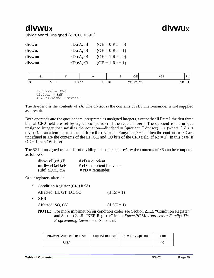
divwux divwuxDivide Word Unsigned (x’7C00 0396’)
divwu rD,rA,rB (OE = 0 Rc = 0)divwu. rD,rA,rB (OE = 0 Rc = 1)divwuo rD,rA,rB (OE = 1 Rc = 0)divwuo. rD,rA,rB (OE = 1 Rc = 1)
dividend ← (rA)divisor ← (rB)rD← dividend ÷ divisor
The dividend is the contents of rA. The divisor is the contents of rB. The remainder is not suppliedas a result.
Both operands and the quotient are interpreted as unsigned integers, except that if Rc = 1 the first threebits of CR0 field are set by signed comparison of the result to zero. The quotient is the uniqueunsigned integer that satisfies the equation—dividend = (quotient ∗ divisor) + r (where 0 ð r <divisor). If an attempt is made to perform the division—<anything> ÷ 0—then the contents of rD areundefined as are the contents of the LT, GT, and EQ bits of the CR0 field (if Rc = 1). In this case, ifOE = 1 then OV is set.
The 32-bit unsigned remainder of dividing the contents of rA by the contents of rB can be computedas follows:
divwurD,rA,rB # rD = quotientmullw rD,rD,rB # rD = quotient ∗ divisorsubf rD,rD,rA # rD = remainder
Other registers altered:
• Condition Register (CR0 field)
Affected: LT, GT, EQ, SO (if Rc = 1)
• XER
Affected: SO, OV (if OE = 1)
NOTE: For more information on condition codes see Section 2.1.3, “Condition Register,” and Section 2.1.5, “XER Register,” in the PowerPC Microprocessor Family: The Programming Environments manual.
0 5 6 10 11 15 16 20 21 22 30 31
31 D A B OE 459 Rc
PowerPC Architecture Level Supervisor Level PowerPC Optional Form
UISA XO
T
able of Contents 5/9/02 Page 49
eciwx eciwxExternal Control In Word Indexed (x’7C00 026C’)
eciwx rD,rA,rB
The eciwx instruction and the EAR register can be very efficient when mapping special devices suchas graphics devices that use addresses as pointers.
if rA = 0 then b ← 0else b← (rA)
EA ← b + (rB)paddr ← address translation of EAsend load word request for paddr to device identified by EAR[RID]rD ← word from device
EA is the sum (rA|0) + (rB).A load word request for the physical address (referred to as real address in the architecturespecification) corresponding to EA is sent to the device identified by EAR[RID], bypassing the cache.The word returned by the device is placed in rD. EAR[E] must be 1. If it is not, a DSI exception is generated. EA must be a multiple of four. If it is not, one of the following occurs:
• A system alignment exception is generated.• A DSI exception is generated (possible only if EAR[E] = 0).• The results are boundedly undefined.
The eciwx instruction is supported for EAs that reference memory segments in which SR[T] = 1(orSTE[T] = 1) and for EAs mapped by the DBAT registers. If the EA references a direct-store segment(SR[T] = 1 or STE[T] = 1), either a DSI exception occurs or the results are boundedly undefined.However, note that the direct-store facility is being phased out of the architecture and will not likelybe supported in future devices. Thus, software should not depend on its effects.If this instruction is executed when MSR[DR] = 0 (real addressing mode), the results are boundedlyundefined. This instruction is treated as a load from the addressed byte with respect to address translation,memory protection, referenced and changed bit recording, and the ordering performed by eieio.This instruction is optional in the PowerPC architecture.Other registers altered:
• None
0 5 6 10 11 15 16 20 21 30 31
Reserved
31 D A B 310 0
PowerPC Architecture Level Supervisor Level PowerPC Optional Form
VEA X X
P
age 50 Version 1.1 IBM PowerPC 750CX/750CXe RISC Microprocessor U ser’s Manual
ecowx ecowxExternal Control Out Word Indexed (x’7C00 036C’)
ecowx rS,rA,rB
The ecowx instruction and the EAR register can be very efficient when mapping special devices suchas graphics devices that use addresses as pointers.
if rA = 0 then b ← 0else b ← (rA)
EA ← b + (rB)paddr ← address translation of EAsend store word request for paddr to device identified by EAR[RID]send rS to device
EA is the sum (rA|0) + (rB).A store word request for the physical address corresponding to EA and the contents of rS are sent tothe device identified by EAR[RID], bypassing the cache. EAR[E] must be 1, if it is not, a DSI exception is generated.EA must be a multiple of four. If it is not, one of the following occurs:
• A system alignment exception is generated.• A DSI exception is generated (possible only if EAR[E] = 0).• The results are boundedly undefined.
The ecowx instruction is supported for effective addresses that reference memory segments in whichSR[T] = 0 or STE[T] = 0), and for EAs mapped by the DBAT registers. If the EA references adirect-store segment (SR[T] = 1 or STE[T] = 1), either a DSI exception occurs or the results areboundedly undefined. However, note that the direct-store facility is being phased out of thearchitecture and will not likely be supported in future devices. Thus, software should not depend onits effects.If this instruction is executed when MSR[DR] = 0 (real addressing mode), the results are boundedlyundefined.This instruction is treated as a store from the addressed byte with respect to address translation,memory protection, and referenced and changed bit recording, and the ordering performed by eieio.Note that software synchronization is required in order to ensure that the data access is performed inprogram order with respect to data accesses caused by other store or ecowx instructions, even thoughthe addressed byte is assumed to be caching-inhibited and guarded.This instruction is optional in the PowerPC architecture.Other registers altered: None
0 5 6 10 11 15 16 20 21 30 31
Reserved
31 S A B 438 0
PowerPC Architecture Level Supervisor Level PowerPC Optional Form
VEA X X
T
able of Contents 5/9/02 Page 51
eieio eieioEnforce In-Order Execution of I/O (x’7C00 06AC’)
The eieio instruction provides an ordering function for the effects of load and store instructionsexecuted by a processor. These loads and stores are divided into two sets, which are orderedseparately. The memory accesses caused by a dcbz or a dcba instruction are ordered like a store. Thetwo sets follow:
1. Loads and stores to memory that is both caching-inhibited and guarded, and stores to memory that is write-through required.
The eieio instruction controls the order in which the accesses are performed in main memory. It ensures that all applicable memory accesses caused by instructions preceding the eieio instruction have completed with respect to main memory before any applicable memory accesses caused by instructions following the eieio instruction access main memory. It acts like a barrier that flows through the memory queues and to main memory, preventing the reordering of memory accesses across the barrier. No ordering is performed for dcbz if the instruction causes the system alignment error handler to be invoked.
All accesses in this set are ordered as a single set—that is, there is not one order for loads and stores to caching-inhibited and guarded memory and another order for stores to write-through required memory.
2. Stores to memory that have all of the following attributes—caching-allowed, write-through not required, and memory-coherency required.
The eieio instruction controls the order in which the accesses are performed with respect to coherent memory. It ensures that all applicable stores caused by instructions preceding the eieio instruction have completed with respect to coherent memory before any applicable stores caused by instructions following the eieio instruction complete with respect to coherent memory.
With the exception of dcbz and dcba, eieio does not affect the order of cache operations (whethercaused explicitly by execution of a cache management instruction, or implicitly by the cachecoherency mechanism). For more information, refer to Chapter 5, “Cache Model and MemoryCoherency” of the PowerPC Microprocessor Family: The Programming Environments manual. Theeieio instruction does not affect the order of accesses in one set with respect to accesses in the otherset.
The eieio instruction may complete before memory accesses caused by instructions preceding theeieio instruction have been performed with respect to main memory or coherent memory asappropriate.
The eieio instruction is intended for use in managing shared data structures, in accessingmemory-mapped I/O, and in preventing load/store combining operations in main memory. For the
0 5 6 10 11 15 16 20 21 30 31
Reserved
31 0 0 0 0 0 0 0 0 0 0 0 0 0 0 0 854 0
P
age 52 Version 1.1 IBM PowerPC 750CX/750CXe RISC Microprocessor U ser’s Manual
first use, the shared data structure and the lock that protects it must be altered only by stores that arein the same set (1 or 2; see previous discussion). For the second use, eieio can be thought of as placinga barrier into the stream of memory accesses issued by a processor, such that any given memoryaccess appears to be on the same side of the barrier to both the processor and the I/O device.
Because the processor performs store operations in order to memory that is designated as bothcaching-inhibited and guarded (refer to Section 5.1.1, “Memory Access Ordering” in the PowerPCMicroprocessor Family: The Programming Environments manual), the eieio instruction is needed forsuch memory only when loads must be ordered with respect to stores or with respect to other loads.
Note that the eieio instruction does not connect hardware considerations to it such as multiprocessorimplementations that send an eieio address-only broadcast (useful in some designs). For example, ifa design has an external buffer that re-orders loads and stores for better bus efficiency, the eieiobroadcast signals to that buffer that previous loads/stores (marked caching-inhibited, guarded, orwrite-through required) must complete before any following loads/stores (marked caching-inhibited,guarded, or write-through required).
Other registers altered:
• None
PowerPC Architecture Level Supervisor Level PowerPC Optional Form
VEA X
T
able of Contents 5/9/02 Page 53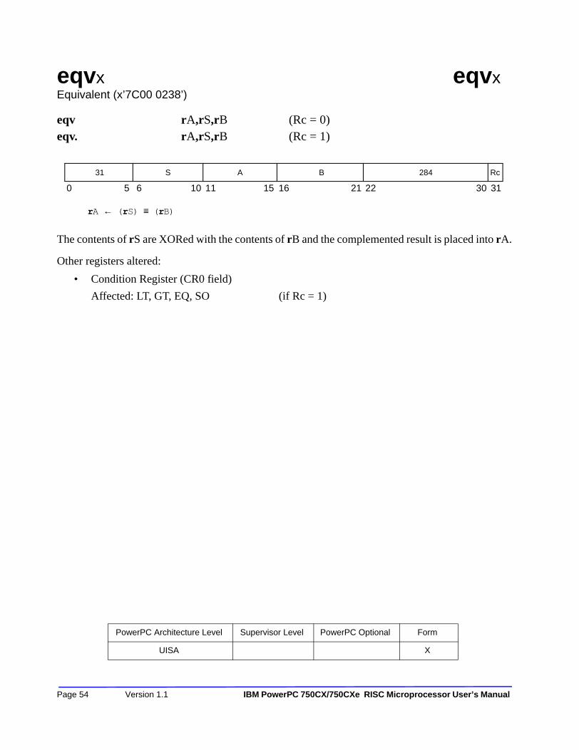
eqvx eqvxEquivalent (x’7C00 0238’)
eqv rA,rS,rB (Rc = 0)eqv. rA,rS,rB (Rc = 1)
rA ← (rS) ≡ (rB)
The contents of rS are XORed with the contents of rB and the complemented result is placed into rA.
Other registers altered:
• Condition Register (CR0 field)
Affected: LT, GT, EQ, SO (if Rc = 1)
0 5 6 10 11 15 16 21 22 30 31
31 S A B 284 Rc
PowerPC Architecture Level Supervisor Level PowerPC Optional Form
UISA X
P
age 54 Version 1.1 IBM PowerPC 750CX/750CXe RISC Microprocessor User’s Manual
extsbx extsbxExtend Sign Byte (x’7C00 0774’)
extsb rA,rS (Rc = 0)extsb. rA,rS (Rc = 1)
S ← rS[24]rA[24-31] ← rS[24-31]rA[0–23] ← (24)S
The contents of the low-order eight bits of rS are placed into the low-order eight bits of rA.
Bit 24 of rS is placed into the remaining bits of rA.
Other registers altered:
• Condition Register (CR0 field)
Affected: LT, GT, EQ, SO (if Rc = 1)
0 5 6 10 11 15 16 20 21 30 31
Reserved
31 S A 0 0 0 0 0 954 Rc
PowerPC Architecture Level Supervisor Level PowerPC Optional Form
UISA X
T
able of Contents 5/9/02 Page 55
extshx extshxExtend Sign Half Word (x’7C00 0734’)
extsh rA,rS (Rc = 0)extsh. rA,rS (Rc = 1)
S ← rS[16]rA[16-31] ← rS[16-31]rA[0–15] ← (16)S
The contents of the low-order 16 bits of rS are placed into the low-order 16 bits of rA[16-31]. Bit 48of rS is placed into the remaining bits of rA.
Other registers altered:
• Condition Register (CR0 field)
Affected: LT, GT, EQ, SO (if Rc = 1)
0 5 6 10 11 15 16 20 21 30 31
Reserved
31 S A 0 0 0 0 0 922 Rc
PowerPC Architecture Level Supervisor Level PowerPC Optional Form
UISA X
P
age 56 Version 1.1 IBM PowerPC 750CX/750CXe RISC Microprocessor U ser’s Manual
fabsx fabsxFloating Absolute Value (x’FC00 0210’)
fabs frD,frB (Rc = 0)fabs. frD,frB (Rc = 1)
The contents of frB with bit 0 cleared are placed into frD.
Note that the fabs instruction treats NaNs just like any other kind of value. That is, the sign bit of aNaN may be altered by fabs. This instruction does not alter the FPSCR.
Other registers altered:
• Condition Register (CR1 field)
Affected: FX, FEX, VX, OX (if Rc = 1)
B 264 Rc
0 5 6 10 11 15 16 20 21 30 31
Reserved
63 D 0 0 0 0 0
PowerPC Architecture Level Supervisor Level PowerPC Optional Form
UISA X
Table of Contents
5/9/02 Page 57
faddx faddxFloating Add (Double-Precision) (x’FC00 002A’)
fadd frD,frA,frB (Rc = 0)fadd. frD,frA,frB (Rc = 1)
The floating-point operand in frA is added to the floating-point operand in frB. If the most-significant bit of the resultant significand is not a one, the result is normalized. The result is roundedto double-precision under control of the floating-point rounding control field RN of the FPSCR andplaced into frD.
Floating-point addition is based on exponent comparison and addition of the two significands. Theexponents of the two operands are compared, and the significand accompanying the smaller exponentis shifted right, with its exponent increased by one for each bit shifted, until the two exponents areequal. The two significands are then added or subtracted as appropriate, depending on the signs of theoperands. All 53 bits in the significand as well as all three guard bits (G, R, and X) enter into thecomputation.
If a carry occurs, the sum's significand is shifted right one bit position and the exponent is increasedby one. FPSCR[FPRF] is set to the class and sign of the result, except for invalid operation exceptionswhen FPSCR[VE] = 1.
Other registers altered:
• Condition Register (CR1 field)
Affected: FX, FEX, VX, OX (if Rc = 1)
• Floating-Point Status and Control Register
Affected: FPRF, FR, FI, FX, OX, UX, XX,VXSNAN, VXISI
0 5 6 10 11 15 16 20 21 25 26 30 31
Reserved
63 D A B 0 0 0 0 0 21 Rc
PowerPC Architecture Level Supervisor Level PowerPC Optional Form
UISA A
P
age 58 Version 1.1 IBM PowerPC 750CX/750CXe RISC Microprocessor U ser’s Manual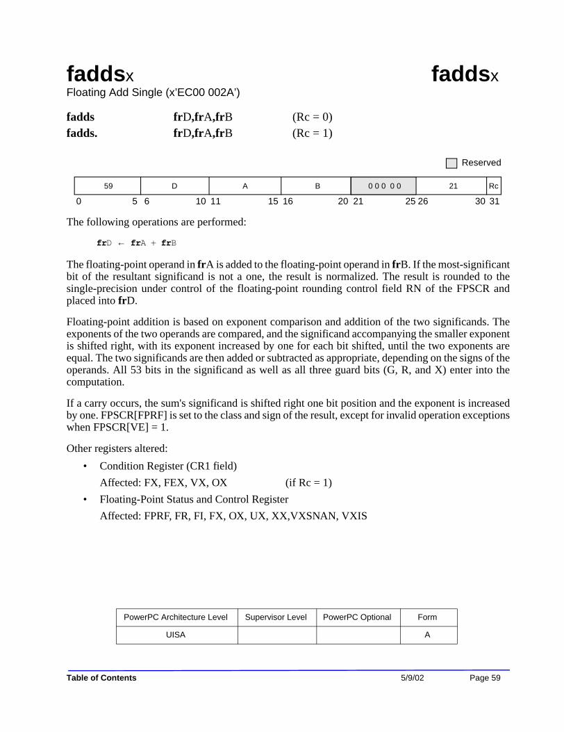
faddsx faddsxFloating Add Single (x’EC00 002A’)
fadds frD,frA,frB (Rc = 0)fadds. frD,frA,frB (Rc = 1)
The following operations are performed:
frD ← frA + frB
The floating-point operand in frA is added to the floating-point operand in frB. If the most-significantbit of the resultant significand is not a one, the result is normalized. The result is rounded to thesingle-precision under control of the floating-point rounding control field RN of the FPSCR andplaced into frD.
Floating-point addition is based on exponent comparison and addition of the two significands. Theexponents of the two operands are compared, and the significand accompanying the smaller exponentis shifted right, with its exponent increased by one for each bit shifted, until the two exponents areequal. The two significands are then added or subtracted as appropriate, depending on the signs of theoperands. All 53 bits in the significand as well as all three guard bits (G, R, and X) enter into thecomputation.
If a carry occurs, the sum's significand is shifted right one bit position and the exponent is increasedby one. FPSCR[FPRF] is set to the class and sign of the result, except for invalid operation exceptionswhen FPSCR[VE] = 1.
Other registers altered:
• Condition Register (CR1 field)
Affected: FX, FEX, VX, OX (if Rc = 1)
• Floating-Point Status and Control Register
Affected: FPRF, FR, FI, FX, OX, UX, XX,VXSNAN, VXIS
0 5 6 10 11 15 16 20 21 25 26 30 31
Reserved
59 D A B 0 0 0 0 0 21 Rc
PowerPC Architecture Level Supervisor Level PowerPC Optional Form
UISA A
T
able of Contents 5/9/02 Page 59
fcmpo fcmpo Floating Compare Ordered (x’FC00 0040’)
fcmpo crfD,frA,frB
if ((frA) is a NaN or (frB) is a NaN) then c ← 0b0001else if (frA)< (frB)
then c ← 0b1000else if (frA)> (frB)
then c ← 0b0100else c ← 0b0010
FPCC ← cCR[(4 * crfD)–(4 * crfD + 3)] ← c
if ((frA) is an SNaN or (frB) is an SNaN)then VXSNAN ← 1
if VE = 0 then VXVC ← 1else if ((frA) is a QNaN or (frB) is a QNaN)
then VXVC ← 1
The floating-point operand in frA is compared to the floating-point operand in frB. The result of thecompare is placed into CR field crfD and the FPCC.
If one of the operands is a NaN, either quiet or signaling, then CR field crfD and the FPCC are set toreflect unordered. If one of the operands is a signaling NaN, then VXSNAN is set, and if invalidoperation is disabled (VE = 0) then VXVC is set. Otherwise, if one of the operands is a QNaN, thenVXVC is set.
Other registers altered:
• Condition Register (CR field specified by operand crfD)
Affected: LT, GT, EQ, UN
• Floating-Point Status and Control Register
Affected: FPCC, FX, VXSNAN, VXVC
0 5 6 8 9 10 11 15 16 20 21 30 31
Reserved
B 32 063 crfD 0 0 A
PowerPC Architecture Level Supervisor Level PowerPC Optional Form
UISA X
P
age 60 Version 1.1 IBM PowerPC 750CX/750CXe RISC Microprocessor U ser’s Manual
fcmpu fcmpu Floating Compare Unordered (x’FC00 0000’)
fcmpu crfD,frA,frB
if ((frA) is a NaN or (frB) is a NaN)then c ← 0b0001else if (frA) < (frB)
then c ← 0b1000else if (frA) > (frB)
then c ← 0b0100else c ← 0b0010
FPCC ← cCR[(4 ∗ crfD)-(4 ∗ crfD + 3)] ← c
if ((frA) is an SNaN or (frB) is an SNaN)then VXSNAN ← 1
The floating-point operand in register frA is compared to the floating-point operand in register frB.The result of the compare is placed into CR field crfD and the FPCC.
If one of the operands is a NaN, either quiet or signaling, then CR field crfD and the FPCC are set toreflect unordered. If one of the operands is a signaling NaN, then VXSNAN is set.
Other registers altered:
• Condition Register (CR field specified by operand crfD)
Affected: LT, GT, EQ, UN
0 5 6 8 9 10 11 15 16 20 21 30 31
Reserved
B 0 0 0 0 0 0 0 0 0 0 063 crfD 0 0 A
PowerPC Architecture Level Supervisor Level PowerPC Optional Form
UISA X
T
able of Contents 5/9/02 Page 61
fctiwx fctiwxFloating Convert to Integer Word (x’FC00 001C’)
fctiw frD,frB (Rc = 0)fctiw. frD,frB (Rc = 1)
The floating-point operand in register frB is converted to a 32-bit signed integer, using the roundingmode specified by FPSCR[RN], and placed in bits 32–63 of frD. Bits 0–31 of frD are undefined.
If the operand in frB are greater than 231 – 1, bits 32–63 of frD are set to 0x7FFF_FFFF.
If the operand in frB are less than –231, bits 32–63 of frD are set to 0x8000_0000.
The conversion is described fully in Section D.4.2, “Floating-Point Convert to Integer Model,” in thePowerPC Microprocessor Family: The Programming Environments manual.
Except for trap-enabled invalid operation exceptions, FPSCR[FPRF] is undefined. FPSCR[FR] is setif the result is incremented when rounded. FPSCR[FI] is set if the result is inexact.
(programmers note: A stiwz instruction should be used to store the 32 bit resultant integer becausebits 0–31 of frD are undefined. A store double-precision instruction, e.g., stfd, will store the 64 bitresult but 4 superfluous bytes are stored (bits frD[0-31]). This may cause wasted bus traffic.)
Other registers altered:
• Condition Register (CR1 field)
Affected: FX, FEX, VX, OX (if Rc = 1)
• Floating-Point Status and Control Register
Affected: FPRF (undefined), FR, FI, FX, XX, VXSNAN, VXCVI
0 5 6 10 11 15 16 20 21 30 31
Reserved
B 14 Rc63 D 0 0 0 0 0
PowerPC Architecture Level Supervisor Level PowerPC Optional Form
UISA X
P
age 62 Version 1.1 IBM PowerPC 750CX/750CXe RISC Microprocessor U ser’s Manual
fctiwzx fctiwzxFloating Convert to Integer Word with Round toward Zero (x’FC00 001E’)
fctiwz frD,frB (Rc = 0)fctiwz. frD,frB (Rc = 1)
The floating-point operand in register frB is converted to a 32-bit signed integer, using the roundingmode round toward zero, and placed in bits 32–63 of frD. Bits 0–31 of frD are undefined.
If the operand in frB is greater than 231 – 1, bits 32–63 of frD are set to 0x7FFF_FFFF.
If the operand in frB is less than –231, bits 32–63 of frD are set to 0x 8000_0000.
The conversion is described fully in Section D.4.2, “Floating-Point Convert to Integer Model” in thePowerPC Microprocessor Family: The Programming Environments manual.
Except for trap-enabled invalid operation exceptions, FPSCR[FPRF] is undefined. FPSCR[FR] is setif the result is incremented when rounded. FPSCR[FI] is set if the result is inexact.
(Programmers Note: A stiwz instruction should be used to store the 32 bit resultant integer becausebits 0–31 of frD are undefined. A store double-precision instruction, e.g., stfd, will store the 64 bitresult but 4 superfluous bytes are stored (bits frD[0-31]). This may cause wasted bus traffic.)
Other registers altered:
• Condition Register (CR1 field)
Affected: FX, FEX, VX, OX (if Rc = 1)
• Floating-Point Status and Control Register
Affected: FPRF (undefined), FR, FI, FX, XX, VXSNAN, VXCVI
0 5 6 10 11 15 16 20 21 30 31
Reserved
B 15 Rc63 D 0 0 0 0 0
PowerPC Architecture Level Supervisor Level PowerPC Optional Form
UISA X
T
able of Contents 5/9/02 Page 63
fdivx fdivxFloating Divide (Double-Precision),(x’FC00 0024’)
fdiv frD,frA,frB (Rc = 0)fdiv. frD,frA,frB (Rc = 1)
The floating-point operand in register frA is divided by the floating-point operand in register frB. Theremainder is not supplied as a result.
If the most-significant bit of the resultant significand is not a one, the result is normalized. The resultis rounded to double-precision under control of the floating-point rounding control field RN of theFPSCR and placed into frD.
Floating-point division is based on exponent subtraction and division of the significands.
FPSCR[FPRF] is set to the class and sign of the result, except for invalid operation exceptions whenFPSCR[VE] = 1 and zero divide exceptions when FPSCR[ZE] = 1.
Other registers altered:
• Condition Register (CR1 field)
Affected: FX, FEX, VX, OX (if Rc = 1)
• Floating-Point Status and Control Register
Affected: FPRF, FR, FI, FX, OX, UX, ZX, XX, VXSNAN, VXIDI, VXZDZ
0 5 6 10 11 15 16 20 21 25 26 30 31
Reserved
B 0 0 0 0 0 18 Rc63 D A
PowerPC Architecture Level Supervisor Level PowerPC Optional Form
UISA A
P
age 64 Version 1.1 IBM PowerPC 750CX/750CXe RISC Microprocessor U ser’s Manual
fdivsx fdivsxFloating Divide Single (x’EC00 0024’)
fdivs frD,frA,frB (Rc = 0)fdivs. frD,frA,frB (Rc = 1)
The floating-point operand in register frA is divided by the floating-point operand in register frB. Theremainder is not supplied as a result.
If the most-significant bit of the resultant significand is not a one, the result is normalized. The resultis rounded to single-precision under control of the floating-point rounding control field RN of theFPSCR and placed into frD.
Floating-point division is based on exponent subtraction and division of the significands.
FPSCR[FPRF] is set to the class and sign of the result, except for invalid operation exceptions whenFPSCR[VE] = 1 and zero divide exceptions when FPSCR[ZE] = 1.
Other registers altered:
• Condition Register (CR1 field):
Affected: FX, FEX, VX, OX (if Rc = 1)
• Floating-Point Status and Control Register:
Affected: FPRF, FR, FI, FX, OX, UX, ZX, XX, VXSNAN, VXIDI, VXZDZ
0 5 6 10 11 15 16 20 21 25 26 30 31
Reserved
B 0 0 0 0 0 18 Rc59 D A
PowerPC Architecture Level Supervisor Level PowerPC Optional Form
UISA A
T
able of Contents 5/9/02 Page 65
fmaddx fmaddxFloating Multiply-Add (Double-Precision),(x’FC00 003A’)
fmadd frD,frA,frC,frB (Rc = 0)fmadd. frD,frA,frC,frB (Rc = 1)
The following operation is performed:
frD ← (frA ∗ frC) + frB
The floating-point operand in register frA is multiplied by the floating-point operand in register frC.The floating-point operand in register frB is added to this intermediate result.
If the most-significant bit of the resultant significand is not a one, the result is normalized. The resultis rounded to double-precision under control of the floating-point rounding control field RN of theFPSCR and placed into frD.
FPSCR[FPRF] is set to the class and sign of the result, except for invalid operation exceptions whenFPSCR[VE] = 1.
Other registers altered:
• Condition Register (CR1 field):
Affected: FX, FEX, VX, OX (if Rc = 1)
• Floating-Point Status and Control Register:
Affected: FPRF, FR, FI, FX, OX, UX, XX, VXSNAN, VXISI, VXIMZ
0 5 6 10 11 15 16 20 21 25 26 30 31
B C 29 Rc63 D A
PowerPC Architecture Level Supervisor Level PowerPC Optional Form
UISA A
P
age 66 Version 1.1 IBM PowerPC 750CX/750CXe RISC Microprocessor User’s Manual
fmaddsx fmaddsxFloating Multiply-Add Single (x’EC00 003A’)
fmadds frD,frA,frC,frB (Rc = 0) fmadds. frD,frA,frC,frB (Rc = 1)
The followings operation are performed:
frD ← (frA ∗ frC) + frB
The floating-point operand in register frA is multiplied by the floating-point operand in register frC.The floating-point operand in register frB is added to this intermediate result.
If the most-significant bit of the resultant significand is not a one, the result is normalized. The resultis rounded to single-precision under control of the floating-point rounding control field RN of theFPSCR and placed into frD.
FPSCR[FPRF] is set to the class and sign of the result, except for invalid operation exceptions whenFPSCR[VE] = 1.
Other registers altered:
• Condition Register (CR1 field):
Affected: FX, FEX, VX, OX (if Rc = 1)
• Floating-Point Status and Control Register:
Affected: FPRF, FR, FI, FX, OX, UX, XX, VXSNAN, VXISI, VXIMZ
0 5 6 10 11 15 16 20 21 25 26 30 31
B C 29 Rc59 D A
PowerPC Architecture Level Supervisor Level PowerPC Optional Form
UISA A
T
able of Contents 5/9/02 Page 67
fmrx fmrxFloating Move Register(Double-Precision),(x’FC00 0090’)
fmr frD,frB (Rc = 0)fmr. frD,frB (Rc = 1)
The content of register frB is placed into frD.
Other registers altered:
• Condition Register (CR1 field):
Affected: FX, FEX, VX, OX (if Rc = 1)
0 5 6 10 11 15 16 20 21 30 31
Reserved
B 72 Rc63 D 0 0 0 0 0
PowerPC Architecture Level Supervisor Level PowerPC Optional Form
UISA X
P
age 68 Version 1.1 IBM PowerPC 750CX/750CXe RISC Microprocessor U ser’s Manual
fmsubx fmsubxFloating Multiply-Subtract (Double-Precision),(x’FC00 0038’)
fmsub frD,frA,frC,frB (Rc = 0)fmsub. frD,frA,frC,frB (Rc = 1)
The following operation is performed:
frD ← [frA ∗ frC] – frB
The floating-point operand in register frA is multiplied by the floating-point operand in register frC.The floating-point operand in register frB is subtracted from this intermediate result.
If the most-significant bit of the resultant significand is not a one, the result is normalized. The resultis rounded to double-precision under control of the floating-point rounding control field RN of theFPSCR and placed into frD.
FPSCR[FPRF] is set to the class and sign of the result, except for invalid operation exceptions whenFPSCR[VE] = 1.
Other registers altered:
• Condition Register (CR1 field):
Affected: FX, FEX, VX, OX (if Rc = 1)
• Floating-Point Status and Control Register:
Affected: FPRF, FR, FI, FX, OX, UX, XX, VXSNAN, VXISI, VXIMZ
0 5 6 10 11 15 16 20 21 25 26 30 31
B C 28 Rc63 D A
PowerPC Architecture Level Supervisor Level PowerPC Optional Form
UISA A
T
able of Contents 5/9/02 Page 69
fmsubsx fmsubsxFloating Multiply-Subtract Single (x’EC00 0038’)
fmsubs frD,frA,frC,frB (Rc = 0)fmsubs. frD,frA,frC,frB (Rc = 1)
The following operations are performed:
frD ← [frA ∗ frC] – frB
The floating-point operand in register frA is multiplied by the floating-point operand in register frC.The floating-point operand in register frB is subtracted from this intermediate result.
If the most-significant bit of the resultant significand is not a one, the result is normalized. The resultis rounded to single-precision under control of the floating-point rounding control field RN of theFPSCR and placed into frD.
FPSCR[FPRF] is set to the class and sign of the result, except for invalid operation exceptions whenFPSCR[VE] = 1.
Other registers altered:
• Condition Register (CR1 field):
Affected: FX, FEX, VX, OX (if Rc = 1)
• Floating-Point Status and Control Register:
Affected: FPRF, FR, FI, FX, OX, UX, XX, VXSNAN, VXISI, VXIMZ
0 5 6 10 11 15 16 20 21 25 26 30 31
B C 28 Rc59 D A
PowerPC Architecture Level Supervisor Level PowerPC Optional Form
UISA A
P
age 70 Version 1.1 IBM PowerPC 750CX/750CXe RISC Microprocessor User’s Manual
fmulx fmulxFloating Multiply (Double-Precision),(x’FC00 0032’)
fmul frD,frA,frC (Rc = 0)fmul. frD,frA,frC (Rc = 1)
The floating-point operand in register frA is multiplied by the floating-point operand in register frC.
If the most-significant bit of the resultant significand is not a one, the result is normalized. The resultis rounded to double-precision under control of the floating-point rounding control field RN of theFPSCR and placed into frD.
Floating-point multiplication is based on exponent addition and multiplication of the significands.
FPSCR[FPRF] is set to the class and sign of the result, except for invalid operation exceptions whenFPSCR[VE] = 1.
Other registers altered:
• Condition Register (CR1 field):
Affected: FX, FEX, VX, OX (if Rc = 1)
• Floating-Point Status and Control Register:
Affected: FPRF, FR, FI, FX, OX, UX, XX, VXSNAN, VXIMZ
0 5 6 10 11 15 16 20 21 25 26 30 31
Reserved
0 0 0 0 0 C 25 Rc63 D A
PowerPC Architecture Level Supervisor Level PowerPC Optional Form
UISA A
T
able of Contents 5/9/02 Page 71
fmulsx fmulsxFloating Multiply Single (x’EC00 0032’)
fmuls frD,frA,frC (Rc = 0)fmuls. frD,frA,frC (Rc = 1)
The following operations are performed:
frD ← frA ∗ frC
The floating-point operand in register frA is multiplied by the floating-point operand in register frC.
If the most-significant bit of the resultant significand is not a one, the result is normalized. The resultis rounded to single-precision under control of the floating-point rounding control field RN of theFPSCR and placed into frD.
Floating-point multiplication is based on exponent addition and multiplication of the significands.
FPSCR[FPRF] is set to the class and sign of the result, except for invalid operation exceptions whenFPSCR[VE] = 1.
Other registers altered:
• Condition Register (CR1 field):
Affected: FX, FEX, VX, OX (if Rc = 1)
• Floating-Point Status and Control Register:
Affected: FPRF, FR, FI, FX, OX, UX, XX, VXSNAN, VXIMZ
0 5 6 10 11 15 16 20 21 25 26 30 31
Reserved
0 0 0 0 0 C 25 Rc59 D A
PowerPC Architecture Level Supervisor Level PowerPC Optional Form
UISA A
P
age 72 Version 1.1 IBM PowerPC 750CX/750CXe RISC Microprocessor U ser’s Manual
fnabsx fnabsxFloating Negative Absolute Value (x’FC00 0110’)
fnabs frD,frB (Rc = 0)fnabs. frD,frB (Rc = 1)
The contents of register frB with bit 0 set are placed into frD.
Note that the fnabs instruction treats NaNs just like any other kind of value. That is, the sign bit of aNaN may be altered by fnabs. This instruction does not alter the FPSCR.
Other registers altered:
• Condition Register (CR1 field):
Affected: FX, FEX, VX, OX (if Rc = 1)
0 5 6 10 11 15 16 20 21 30 31
Reserved
B 136 Rc63 D 0 0 0 0 0
PowerPC Architecture Level Supervisor Level PowerPC Optional Form
UISA X
T
able of Contents 5/9/02 Page 73
fnegx fnegxFloating Negate (x’FC00 0050’)
fneg frD,frB (Rc = 0)fneg. frD,frB (Rc = 1)
The contents of register frB with bit 0 inverted are placed into frD.
Note that the fneg instruction treats NaNs just like any other kind of value. That is, the sign bit of aNaN may be altered by fneg. This instruction does not alter the FPSCR.
Other registers altered:
• Condition Register (CR1 field):
Affected: FX, FEX, VX, OX (if Rc = 1)
0 5 6 10 11 15 16 20 21 30 31
Reserved
B 40 Rc63 D 0 0 0 0 0
PowerPC Architecture Level Supervisor Level PowerPC Optional Form
UISA X
P
age 74 Version 1.1 IBM PowerPC 750CX/750CXe RISC Microprocessor U ser’s Manual
fnmaddx fnmaddx Floating Negative Multiply-Add (Double-Precision),(x’FC00 003E’)
fnmadd frD,frA,frC,frB (Rc = 0)fnmadd. frD,frA,frC,frB (Rc = 1)
The following operation is performed:
frD ← – ([frA ∗ frC] + frB)
The floating-point operand in register frA is multiplied by the floating-point operand in register frC.The floating-point operand in register frB is added to this intermediate result. If the most-significantbit of the resultant significand is not a one, the result is normalized. The result is rounded todouble-precision under control of the floating-point rounding control field RN of the FPSCR, thennegated and placed into frD.
This instruction produces the same result as would be obtained by using the Floating Multiply-Add(fmaddx) instruction and then negating the result, with the following exceptions:
• QNaNs propagate with no effect on their sign bit.
• QNaNs that are generated as the result of a disabled invalid operation exception have a sign bit of zero.
• SNaNs that are converted to QNaNs as the result of a disabled invalid operation exception retain the sign bit of the SNaN.
FPSCR[FPRF] is set to the class and sign of the result, except for invalid operation exceptions whenFPSCR[VE] = 1.
Other registers altered:
• Condition Register (CR1 field):
Affected: FX, FEX, VX, OX (if Rc = 1)
• Floating-Point Status and Control Register:
Affected: FPRF, FR, FI, FX, OX, UX, XX, VXSNAN, VXISI, VXIMZ
0 5 6 10 11 15 16 20 21 25 26 30 31
B C 31 Rc63 D A
PowerPC Architecture Level Supervisor Level PowerPC Optional Form
UISA A
T
able of Contents 5/9/02 Page 75
fnmaddsx fnmaddsx Floating Negative Multiply-Add Single (x’EC00 003E’)
fnmadds frD,frA,frC,frB (Rc = 0)fnmadds. frD,frA,frC,frB (Rc = 1)
The following operations are performed:
frD ← -([frA ∗ frC] + frB)
The floating-point operand in register frA is multiplied by the floating-point operand in register frC.The floating-point operand in register frB is added to this intermediate result. If the most-significantbit of the resultant significand is not a one, the result is normalized. The result is rounded tosingle-precision under control of the floating-point rounding control field RN of the FPSCR, thennegated and placed into frD.
This instruction produces the same result as would be obtained by using the Floating Multiply-AddSingle (fmaddsx) instruction and then negating the result, with the following exceptions:
• QNaNs propagate with no effect on their sign bit.
• QNaNs that are generated as the result of a disabled invalid operation exception have a sign bit of zero.
• SNaNs that are converted to QNaNs as the result of a disabled invalid operation exception retain the sign bit of the SNaN.
FPSCR[FPRF] is set to the class and sign of the result, except for invalid operation exceptions whenFPSCR[VE] = 1.
Other registers altered:
• Condition Register (CR1 field):
Affected: FX, FEX, VX, OX (if Rc = 1)
• Floating-Point Status and Control Register:
Affected: FPRF, FR, FI, FX, OX, UX, XX, VXSNAN, VXISI, VXIMZ
0 5 6 10 11 15 16 20 21 25 26 30 31
B C 31 Rc59 D A
PowerPC Architecture Level Supervisor Level PowerPC Optional Form
UISA A
P
age 76 Version 1.1 IBM PowerPC 750CX/750CXe RISC Microprocessor User’s Manual
fnmsubx fnmsubxFloating Negative Multiply-Subtract (Double-Precision),(x’FC00 003C’)
fnmsub frD,frA,frC,frB (Rc = 0)fnmsub. frD,frA,frC,frB (Rc = 1)
]
The following operation is performed:
frD ← – ([frA ∗ frC] – frB)The floating-point operand in register frA is multiplied by the floating-point operand in register frC.The floating-point operand in register frB is subtracted from this intermediate result.
If the most-significant bit of the resultant significand is not one, the result is normalized. The resultis rounded to double-precision under control of the floating-point rounding control field RN of theFPSCR, then negated and placed into frD.
This instruction produces the same result obtained by negating the result of a FloatingMultiply-Subtract (fmsubx) instruction with the following exceptions:
• QNaNs propagate with no effect on their sign bit.
• QNaNs that are generated as the result of a disabled invalid operation exception have a sign bit of zero.
• SNaNs that are converted to QNaNs as the result of a disabled invalid operation exception retain the sign bit of the SNaN.
FPSCR[FPRF] is set to the class and sign of the result, except for invalid operation exceptions whenFPSCR[VE] = 1.
Other registers altered:
• Condition Register (CR1 field)
Affected: FX, FEX, VX, OX (if Rc = 1)
• Floating-Point Status and Control Register
Affected: FPRF, FR, FI, FX, OX, UX, XX, VXSNAN, VXISI, VXIMZ
0 5 6 10 11 15 16 20 21 25 26 30 31
B C 30 Rc63 D A
PowerPC Architecture Level Supervisor Level PowerPC Optional Form
UISA A
T
able of Contents 5/9/02 Page 77
fnmsubsx fnmsubsxFloating Negative Multiply-Subtract Single (x’EC00 003C’)
fnmsubs frD,frA,frC,frB (Rc = 0)fnmsubs. frD,frA,frC,frB (Rc = 1)
)
The following operations are performed:
frD ← -([frA ∗ frC] - frB)
The floating-point operand in register frA is multiplied by the floating-point operand in register frC.The floating-point operand in register frB is subtracted from this intermediate result.
If the most-significant bit of the resultant significand is not one, the result is normalized. The resultis rounded to single-precision under control of the floating-point rounding control field RN of theFPSCR, then negated and placed into frD.
This instruction produces the same result obtained by negating the result of a FloatingMultiply-Subtract Single (fmsubsx) instruction with the following exceptions:
• QNaNs propagate with no effect on their sign bit.
• QNaNs that are generated as the result of a disabled invalid operation exception have a sign bit of zero.
• SNaNs that are converted to QNaNs as the result of a disabled invalid operation exception retain the sign bit of the SNaN.
FPSCR[FPRF] is set to the class and sign of the result, except for invalid operation exceptions whenFPSCR[VE] = 1.
Other registers altered:
• Condition Register (CR1 field)
Affected: FX, FEX, VX, OX (if Rc = 1)
• Floating-Point Status and Control Register
Affected: FPRF, FR, FI, FX, OX, UX, XX, VXSNAN, VXISI, VXIMZ
0 5 6 10 11 15 16 20 21 25 26 30 31
B C 30 Rc59 D A
PowerPC Architecture Level Supervisor Level PowerPC Optional Form
UISA A
P
age 78 Version 1.1 IBM PowerPC 750CX/750CXe RISC Microprocessor User’s Manual
fresx fresxFloating Reciprocal Estimate Single (x’EC00 0030’)
fres frD,frB (Rc = 0)fres. frD,frB (Rc = 1)
frD ← estimate[1/frB]
A single-precision estimate of the reciprocal of the floating-point operand in register frB is placedinto register frD. The estimate placed into register frD is correct to a precision of one part in 4096 ofthe reciprocal of frB. That is,
where x is the initial value in frB. Note that the value placed into register frD may vary betweenimplementations, and between different executions on the same implementation.
Operation with various special values of the operand is summarized below:
Operand Result Exception
–× –0 None
–0 –×* ZX
+0 +×* ZX
+× +0 None
SNaN QNaN** VXSNAN
QNaN QNaN None
Notes: * No result if FPSCR[ZE] = 1
** No result if FPSCR[VE] = 1
FPSCR[FPRF] is set to the class and sign of the result, except for invalid operation exceptions whenFPSCR[VE] = 1 and zero divide exceptions when FPSCR[ZE] = 1.
NOTE: The PowerPC architecture makes no provision for a double-precision version of the fresx instruction. This is because graphics applications are expected to need only the single-precision version, and no other important performance-critical applications are expected to require a double-precision version of the fresx instruction.
B 0 0 0 0 0 24 Rc
0 5 6 10 11 15 16 20 21 25 26 30 31
Reserved
59 D 0 0 0 0 0
ABSestimate 1
x--- –
1x---
-------------------------------------
14096( )
------------------≤
Table of Contents
5/9/02 Page 79
This instruction is optional in the PowerPC architecture. Other registers altered:
• Condition Register (CR1 field)
Affected: FX, FEX, VX, OX (if Rc = 1)
• Floating-Point Status and Control Register
Affected: FPRF, FR (undefined), FI (undefined), FX, OX, UX, ZX, VXSNAN
PowerPC Architecture Level Supervisor Level PowerPC Optional Form
UISA YES A
P
age 80 Version 1.1 IBM PowerPC 750CX/750CXe RISC Microprocessor User’s Manual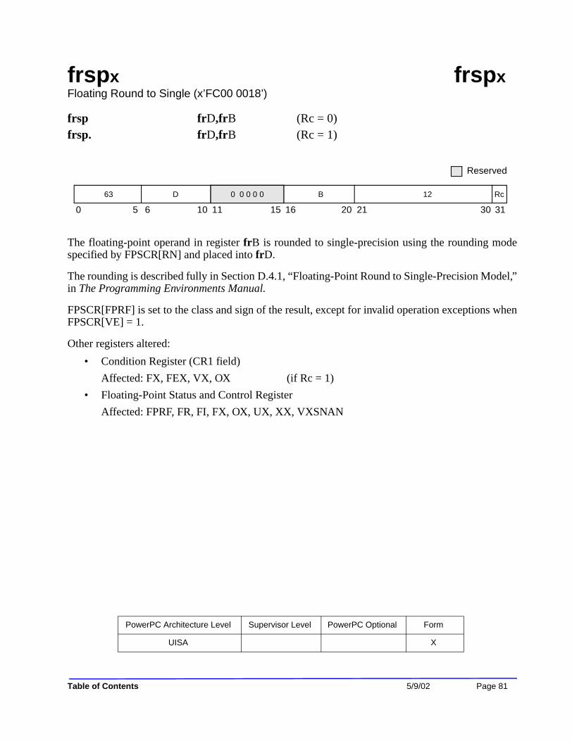
frspx frspxFloating Round to Single (x’FC00 0018’)
frsp frD,frB (Rc = 0)frsp. frD,frB (Rc = 1)
The floating-point operand in register frB is rounded to single-precision using the rounding modespecified by FPSCR[RN] and placed into frD.
The rounding is described fully in Section D.4.1, “Floating-Point Round to Single-Precision Model,”in The Programming Environments Manual.
FPSCR[FPRF] is set to the class and sign of the result, except for invalid operation exceptions whenFPSCR[VE] = 1.
Other registers altered:
• Condition Register (CR1 field)
Affected: FX, FEX, VX, OX (if Rc = 1)
• Floating-Point Status and Control Register
Affected: FPRF, FR, FI, FX, OX, UX, XX, VXSNAN
0 5 6 10 11 15 16 20 21 30 31
Reserved
B 12 Rc63 D 0 0 0 0 0
PowerPC Architecture Level Supervisor Level PowerPC Optional Form
UISA X
T
able of Contents 5/9/02 Page 81
frsqrtex frsqrtexFloating Reciprocal Square Root Estimate (x’FC00 0034’)
frsqrte frD,frB (Rc = 0)frsqrte. frD,frB (Rc = 1)
A double-precision estimate of the reciprocal of the square root of the floating-point operand inregister frB is placed into register frD. The estimate placed into register frD is correct to a precisionof one part in 4096 of the reciprocal of the square root of frB. That is,
where x is the initial value in frB. Note that the value placed into register frD may vary betweenimplementations, and between different executions on the same implementation.
Operation with various special values of the operand is summarized below:
Operand Result Exception
–× QNaN** VXSQRT
<0 QNaN** VXSQRT
–0 –×* ZX
+0 +×* ZX
+× +0 None
SNaN QNaN** VXSNAN
QNaN QNaN None
Notes: * No result if FPSCR[ZE] = 1
** No result if FPSCR[VE] = 1
FPSCR[FPRF] is set to the class and sign of the result, except for invalid operation exceptions whenFPSCR[VE] = 1 and zero divide exceptions when FPSCR[ZE] = 1.
NOTE: No single-precision version of the frsqrte instruction is provided; however, both frB and frD are representable in single-precision format.
This instruction is optional in the PowerPC architecture.
0 5 6 10 11 15 16 20 21 25 26 30 31
Reserved
63 D 0 0 0 0 0 B 0 0 0 0 0 26 Rc
ABS
estimate 1
x------- –
1
x-------
-----------------------------------------
14096-------------≤
P
age 82 Version 1.1 IBM PowerPC 750CX/750CXe RISC Microprocessor U ser’s Manual
Other registers altered:
• Condition Register (CR1 field)
Affected: FX, FEX, VX, OX (if Rc = 1)
• Floating-Point Status and Control Register
Affected: FPRF, FR (undefined), FI (undefined), FX, ZX, VXSNAN, VXSQRT
PowerPC Architecture Level Supervisor Level PowerPC Optional Form
UISA Yes A
T
able of Contents 5/9/02 Page 83
fselx fselxFloating Select (x’FC00 002E’)
fsel frD,frA,frC,frB (Rc = 0)fsel. frD,frA,frC,frB (Rc = 1)
if (frA) ≥ 0.0 then frD ← (frC)else frD ← (frB)
The floating-point operand in register frA is compared to the value zero. If the operand is greater thanor equal to zero, register frD is set to the contents of register frC. If the operand is less than zero oris a NaN, register frD is set to the contents of register frB. The comparison ignores the sign of zero(that is, regards +0 as equal to –0).
Care must be taken in using fsel if IEEE compatibility is required, or if the values being tested can beNaNs or infinities.
For examples of uses of this instruction, see Section D.3, “Floating-Point Conversions,” andSection D.5, “Floating-Point Selection,” in The Programming Environments Manual.
This instruction is optional in the PowerPC architecture.
Other registers altered:
• Condition Register (CR1 field)
Affected: FX, FEX, VX, OX (if Rc = 1)
B C 23 Rc
0 5 6 10 11 15 16 20 21 25 26 30 31
63 D A
PowerPC Architecture Level Supervisor Level PowerPC Optional Form
UISA Yes A
Page 84 Version 1.1
IBM PowerPC 750CX/750CXe RISC Microprocessor User’s Manual
fsubx fsubxFloating Subtract (Double-Precision),(x’FC00 0028’)
fsub frD,frA,frB (Rc = 0)fsub. frD,frA,frB (Rc = 1)
The floating-point operand in register frB is subtracted from the floating-point operand in registerfrA. If the most-significant bit of the resultant significand is not a one, the result is normalized. Theresult is rounded to double-precision under control of the floating-point rounding control field RN ofthe FPSCR and placed into frD.
The execution of the fsub instruction is identical to that of fadd, except that the contents of frBparticipate in the operation with its sign bit (bit 0) inverted.
FPSCR[FPRF] is set to the class and sign of the result, except for invalid operation exceptions whenFPSCR[VE] = 1.
Other registers altered:
• Condition Register (CR1 field)
Affected: FX, FEX, VX, OX (if Rc = 1)
• Floating-Point Status and Control Register
Affected: FPRF, FR, FI, FX, OX, UX, XX, VXSNAN, VXISI
0 5 6 10 11 15 16 20 21 25 26 30 31
Reserved
B 0 0 0 0 0 20 Rc63 D A
PowerPC Architecture Level Supervisor Level PowerPC Optional Form
UISA A
T
able of Contents 5/9/02 Page 85
fsubsx fsubsxFloating Subtract Single (x’EC00 0028’)
fsubs frD,frA,frB (Rc = 0)fsubs. frD,frA,frB (Rc = 1)
The following operations are performed:
frD ← frA – frB
The floating-point operand in register frB is subtracted from the floating-point operand in registerfrA. If the most-significant bit of the resultant significand is not a one, the result is normalized. Theresult is rounded to single-precision under control of the floating-point rounding control field RN ofthe FPSCR and placed into frD.
The execution of the fsubs instruction is identical to that of fadds, except that the contents of frBparticipate in the operation with its sign bit (bit 0) inverted.
FPSCR[FPRF] is set to the class and sign of the result, except for invalid operation exceptions whenFPSCR[VE] = 1.
Other registers altered:
• Condition Register (CR1 field)
Affected: FX, FEX, VX, OX (if Rc = 1)
• Floating-Point Status and Control Register
Affected: FPRF, FR, FI, FX, OX, UX, XX, VXSNAN, VXISI
0 5 6 10 11 15 16 20 21 25 26 30 31
Reserved
B 0 0 0 0 0 20 Rc59 D A
PowerPC Architecture Level Supervisor Level PowerPC Optional Form
UISA A
P
age 86 Version 1.1 IBM PowerPC 750CX/750CXe RISC Microprocessor U ser’s Manual
icbi icbiInstruction Cache Block Invalidate (x’7C00 07AC’)
icbi rA,rB
EA is the sum (rA|0) + (rB).
If the block containing the byte addressed by EA is in coherency-required mode, and a blockcontaining the byte addressed by EA is in the instruction cache of any processor, the block is madeinvalid in all such instruction caches, so that subsequent references cause the block to be refetched.
If the block containing the byte addressed by EA is in coherency-not-required mode, and a blockcontaining the byte addressed by EA is in the instruction cache of this processor, the block is madeinvalid in that instruction cache, so that subsequent references cause the block to be refetched.
The function of this instruction is independent of the write-through, write-back, andcaching-inhibited/allowed modes of the block containing the byte addressed by EA.
This instruction is treated as a load from the addressed byte with respect to address translation andmemory protection. It may also be treated as a load for referenced and changed bit recording exceptthat referenced and changed bit recording may not occur. Implementations with a combined data andinstruction cache treat the icbi instruction as a no-op, except that they may invalidate the target blockin the instruction caches of other processors if the block is in coherency-required mode.The icbiinstruction invalidates the block at EA (rA|0 + rB). If the processor is a multiprocessorimplementation (for example, the 601, 604, or 620) and the block is marked coherency-required, theprocessor will send an address-only broadcast to other processors causing those processors toinvalidate the block from their instruction caches.
For faster processing, many implementations will not compare the entire EA (rA|0 + rB) with the tagin the instruction cache. Instead, they will use the bits in the EA to locate the set that the block is in,and invalidate all blocks in that set.
Other registers altered:
• None
0 5 6 10 11 15 16 20 21 30 31
Reserved
B 982 031 0 0 0 0 0 A
PowerPC Architecture Level Supervisor Level PowerPC Optional Form
VEA X
T
able of Contents 5/9/02 Page 87
isync isyncInstruction Synchronize (x’4C00 012C’)
isync
The isync instruction provides an ordering function for the effects of all instructions executed by aprocessor. Executing an isync instruction ensures that all instructions preceding the isync instructionhave completed before the isync instruction completes, except that memory accesses caused by thoseinstructions need not have been performed with respect to other processors and mechanisms. It alsoensures that no subsequent instructions are initiated by the processor until after the isync instructioncompletes. Finally, it causes the processor to discard any prefetched instructions, with the effect thatsubsequent instructions will be fetched and executed in the context established by the instructionspreceding the isync instruction. The isync instruction has no effect on the other processors or on theircaches.
This instruction is context synchronizing.
Context synchronization is necessary after certain code sequences that perform complex operationswithin the processor. These code sequences are usually operating system tasks that involve memorymanagement. For example, if an instruction A changes the memory translation rules in the memorymanagement unit (MMU), the isync instruction should be executed so that the instructions followinginstruction A will be discarded from the pipeline and refetched according to the new translation rules.
NOTE: All exceptions and the rfi and sc instructions are also context synchronizing.
Other registers altered:
• None
0 0 0 0 0 150 0
0 5 6 10 11 15 16 20 21 30 31
Reserved
19 0 0 0 0 0 0 0 0 0 0
PowerPC Architecture Level Supervisor Level PowerPC Optional Form
VEA XL
Page 88 Version 1.1
IBM PowerPC 750CX/750CXe RISC Microprocessor U ser’s Manual
lbz lbzLoad Byte and Zero (x’8800 0000’)
lbz rD,d(rA)
if rA = 0 then b ← 0else b ← (rA)EA ← b + EXTS(d)rD ← (24)0 || MEM(EA, 1)
EA is the sum (rA|0) + d. The byte in memory addressed by EA is loaded into the low-order eight bitsof rD. The remaining bits in rD are cleared.
Other registers altered:
• None
0 5 6 10 11 15 16 31
d34 D A
PowerPC Architecture Level Supervisor Level PowerPC Optional Form
UISA D
T
able of Contents 5/9/02 Page 89
lbzu lbzuLoad Byte and Zero with Update (x’8C00 0000’)
lbzu rD,d(rA)
EA ← (rA) + EXTS(d)rD ← (24)0 || MEM(EA, 1)rA ← EA
EA is the sum (rA) + d. The byte in memory addressed by EA is loaded into the low-order eight bitsof rD. The remaining bits in rD are cleared.
EA is placed into rA.
If rA = 0, or rA = rD, the instruction form is invalid.
Other registers altered:
• None
0 5 6 10 11 15 16 31
d35 D A
PowerPC Architecture Level Supervisor Level PowerPC Optional Form
UISA D
P
age 90 Version 1.1 IBM PowerPC 750CX/750CXe RISC Microprocessor User’s Manual
lbzux lbzuxLoad Byte and Zero with Update Indexed (x’7C00 00EE’)
lbzux rD,rA,rB
EA ← (rA) + (rB)rD ← (24)0 || MEM(EA, 1)rA ← EA
EA is the sum (rA) + (rB). The byte in memory addressed by EA is loaded into the low-order eightbits of rD. The remaining bits in rD are cleared.
EA is placed into rA.
If rA = 0 or rA = rD, the instruction form is invalid.
Other registers altered:
• None
0 5 6 10 11 15 16 20 21 30 31
Reserved
B 119 031 D A
PowerPC Architecture Level Supervisor Level PowerPC Optional Form
UISA X
T
able of Contents 5/9/02 Page 91
lbzx lbzxLoad Byte and Zero Indexed (x’7C00 00AE’)
lbzx rD,rA,rB
if rA = 0 then b ← 0else b ← (rA)EA ← b + (rB)rD ← (24)0 || MEM(EA, 1)
EA is the sum (rA|0) + (rB). The byte in memory addressed by EA is loaded into the low-order eightbits of rD. The remaining bits in rD are cleared.
Other registers altered:
• None
0 5 6 10 11 15 16 20 21 30 31
Reserved
B 87 031 D A
PowerPC Architecture Level Supervisor Level PowerPC Optional Form
UISA X
P
age 92 Version 1.1 IBM PowerPC 750CX/750CXe RISC Microprocessor U ser’s Manual
lfd lfd Load Floating-Point Double (x’C800 0000’)
lfd frD,d(rA)
if rA = 0 then b ← 0else b ← (rA)EA ← b + EXTS(d)frD ← MEM(EA, 8)
EA is the sum (rA|0) + d.
The double word in memory addressed by EA is placed into frD.
Other registers altered:
• None
0 5 6 10 11 15 16 31
d50 D A
PowerPC Architecture Level Supervisor Level PowerPC Optional Form
UISA D
T
able of Contents 5/9/02 Page 93
lfdu lfdu Load Floating-Point Double with Update (x’CC00 0000’)
lfdu frD,d(rA)
EA ← (rA) + EXTS(d)frD ← MEM(EA, 8)rA ← EA
EA is the sum (rA) + d.
The double word in memory addressed by EA is placed into frD.
EA is placed into rA.
If rA = 0, the instruction form is invalid.
Other registers altered:
• None
0 5 6 10 11 15 16 31
d51 D A
PowerPC Architecture Level Supervisor Level PowerPC Optional Form
UISA D
P
age 94 Version 1.1 IBM PowerPC 750CX/750CXe RISC Microprocessor User’s Manual
lfdux lfdux Load Floating-Point Double with Update Indexed (x’7C00 04EE’)
lfdux frD,rA,rB
EA ← (rA) + (rB)frD ← MEM(EA, 8)rA ← EA
EA is the sum (rA) + (rB).
The double word in memory addressed by EA is placed into frD.
EA is placed into rA.
If rA = 0, the instruction form is invalid.
Other registers altered:
• None
0 5 6 10 11 15 16 20 21 30 31
Reserved
B 631 031 D A
PowerPC Architecture Level Supervisor Level PowerPC Optional Form
UISA X
T
able of Contents 5/9/02 Page 95
lfdx lfdx Load Floating-Point Double Indexed (x’7C00 04AE’)
lfdx frD,rA,rB
if rA = 0then b ← 0else b ← (rA)EA ← b + (rB)frD ← MEM(EA, 8)
EA is the sum (rA|0) + (rB).
The double word in memory addressed by EA is placed into frD.
Other registers altered:
• None
0 5 6 10 11 15 16 20 21 30 31
Reserved
B 599 031 D A
PowerPC Architecture Level Supervisor Level PowerPC Optional Form
UISA X
P
age 96 Version 1.1 IBM PowerPC 750CX/750CXe RISC Microprocessor U ser’s Manual
lfs lfs Load Floating-Point Single (x’C000 0000’)
lfs frD,d(rA)
if rA = 0 then b ← 0else b ← (rA)EA ← b + EXTS(d)frD ← DOUBLE(MEM(EA, 4))
The word in memory addressed by EA is interpreted as a floating-point single-precision operand andis converted to floating-point double-precision and placed into frD.
Other registers altered:
• None
0 5 6 10 11 15 16 31
d48 D A
PowerPC Architecture Level Supervisor Level PowerPC Optional Form
UISA D
T
able of Contents 5/9/02 Page 97
lfsu lfsu Load Floating-Point Single with Update (x’C400 0000’)
lfsu frD,d(rA)
EA ← (rA) + EXTS(d)rA ← EAfrD ← DOUBLE(MEM(EA, 4))
EA is the sum (rA) + d.
The word in memory addressed by EA is interpreted as a floating-point single-precision operand andis converted to floating-point double-precision and placed into frD.
EA is placed into rA.
If rA = 0, the instruction form is invalid.
Other registers altered:
• None
0 5 6 10 11 15 16 31
d49 D A
PowerPC Architecture Level Supervisor Level PowerPC Optional Form
UISA D
P
age 98 Version 1.1 IBM PowerPC 750CX/750CXe RISC Microprocessor User’s Manual
lfsux lfsux Load Floating-Point Single with Update Indexed (x’7C00 046E’)
lfsux frD,rA,rB
EA ← (rA) + (rB)frD ← DOUBLE(MEM(EA, 4))rA ← EA
EA is the sum (rA) + d.
The word in memory addressed by EA is interpreted as a floating-point single-precision operand andis converted to floating-point double-precision (see Section D.6, “Floating-Point Load Instructions,”in The Programming Environments Manual) and placed into frD.
EA is placed into rA.
If rA = 0, the instruction form is invalid.
Other registers altered:
• None
0 5 6 10 11 15 16 20 21 30 31
Reserved
B 567 031 D A
PowerPC Architecture Level Supervisor Level PowerPC Optional Form
UISA X
T
able of Contents 5/9/02 Page 99
lfsx lfsxLoad Floating-Point Single Indexed (x’7C00 042E’) lfsx frD,rA,rB
if rA = 0 then b ← 0else b ← (rA)EA ← b + (rB)frD ← DOUBLE(MEM(EA, 4))
EA is the sum (rA|0) + (rB).
The word in memory addressed by EA is interpreted as a floating-point single-precision operand andis converted to floating-point double-precision and placed into frD.
Other registers altered:
• None
0 5 6 10 11 15 16 20 21 30 31
Reserved
B 535 031 D A
PowerPC Architecture Level Supervisor Level PowerPC Optional Form
UISA X
P
age 100 Version 1.1 IBM PowerPC 750CX/750CXe RISC Microprocessor U ser’s Manual
lha lha Load Half Word Algebraic (x’A800 0000’)
lha rD,d(rA)
if rA = 0 then b ← 0else b ← (rA)EA ← b + EXTS(d)rD ← EXTS(MEM(EA, 2))
EA is the sum (rA|0) + d. The half word in memory addressed by EA is loaded into the low-order 16bits of rD. The remaining bits in rD are filled with a copy of the most-significant bit of the loadedhalf word.
Other registers altered:
• None
0 5 6 10 11 15 16 31
d42 D A
PowerPC Architecture Level Supervisor Level PowerPC Optional Form
UISA D
T
able of Contents 5/9/02 Page 101
lhau lhauLoad Half Word Algebraic with Update (x’AC00 0000’)
lhau rD,d(rA)
EA ← (rA) + EXTS(d)rD ← EXTS(MEM(EA, 2))rA ← EA
EA is the sum (rA) + d. The half word in memory addressed by EA is loaded into the low-order 16bits of rD. The remaining bits in rD are filled with a copy of the most-significant bit of the loadedhalf word.
EA is placed into rA.
If rA = 0 or rA = rD, the instruction form is invalid.
Other registers altered:
• None
0 5 6 10 11 15 16 31
d43 D A
PowerPC Architecture Level Supervisor Level PowerPC Optional Form
UISA D
P
age 102 Version 1.1 IBM PowerPC 750CX/750CXe RISC Microprocessor User’s Manual
lhaux lhauxLoad Half Word Algebraic with Update Indexed (x’7C00 02EE’)
lhaux rD,rA,rB
EA ← (rA) + (rB)rD ← EXTS(MEM(EA, 2))rA ← EA
EA is the sum (rA) + (rB). The half word in memory addressed by EA is loaded into the low-order16 bits of rD. The remaining bits in rD are filled with a copy of the most-significant bit of the loadedhalf word.
EA is placed into rA.
If rA = 0 or rA = rD, the instruction form is invalid.
Other registers altered:
• None
0 5 6 10 11 15 16 20 21 30 31
Reserved
B 375 031 D A
PowerPC Architecture Level Supervisor Level PowerPC Optional Form
UISA X
T
able of Contents 5/9/02 Page 103
lhax lhaxLoad Half Word Algebraic Indexed (x’7C00 02AE’)
lhax rD,rA,rB
if rA = 0 then b ← 0else b ← (rA)EA ← b + (rB)rD ← EXTS(MEM(EA, 2)
EA is the sum (rA|0) + (rB). The half word in memory addressed by EA is loaded into the low-order16 bits of rD. The remaining bits in rD are filled with a copy of the most-significant bit of the loadedhalf word.
Other registers altered:
• None
0 5 6 10 11 15 16 20 21 30 31
Reserved
B 343 031 D A
PowerPC Architecture Level Supervisor Level PowerPC Optional Form
UISA X
P
age 104 Version 1.1 IBM PowerPC 750CX/750CXe RISC Microprocessor U ser’s Manual
lhbrx lhbrxLoad Half Word Byte-Reverse Indexed (x’7C00 062C’)
lhbrx rD,rA,rB
if rA = 0 then b ← 0else b ← (rA)EA ← b + (rB)rD ← (16)0 || MEM(EA + 1, 1) || MEM(EA, 1)
EA is the sum (rA|0) + (rB). Bits 0–7 of the half word in memory addressed by EA are loaded intothe low-order eight bits of rD. Bits 8–15 of the half word in memory addressed by EA are loaded intothe subsequent low-order eight bits of rD. The remaining bits in rD are cleared.
The PowerPC architecture cautions programmers that some implementations of the architecture mayrun the lhbrx instructions with greater latency than other types of load instructions.
Other registers altered:
• None
0 5 6 10 11 15 16 20 21 30 31
Reserved
B 790 031 D A
PowerPC Architecture Level Supervisor Level PowerPC Optional Form
UISA X
T
able of Contents 5/9/02 Page 105
lhz lhzLoad Half Word and Zero (x’A000 0000’)
lhz rD,d(rA)
if rA = 0 then b ← 0else b ← (rA)EA ← b + EXTS(d)rD ← (16)0 || MEM(EA, 2)
EA is the sum (rA|0) + d. The half word in memory addressed by EA is loaded into the low-order 16bits of rD. The remaining bits in rD are cleared.
Other registers altered:
• None
0 5 6 10 11 15 16 31
d40 D A
PowerPC Architecture Level Supervisor Level PowerPC Optional Form
UISA D
P
age 106 Version 1.1 IBM PowerPC 750CX/750CXe RISC Microprocessor User’s Manual
lhzu lhzuLoad Half Word and Zero with Update (x’A400 0000’)
lhzu rD,d(rA)
EA ← rA + EXTS(d)rD ← (16)0 || MEM(EA, 2)rA ← EA
EA is the sum (rA) + d. The half word in memory addressed by EA is loaded into the low-order 16bits of rD. The remaining bits in rD are cleared.
EA is placed into rA.
If rA = 0 or rA = rD, the instruction form is invalid.
Other registers altered:
• None
0 5 6 10 11 15 16 31
d41 D A
PowerPC Architecture Level Supervisor Level PowerPC Optional Form
UISA D
T
able of Contents 5/9/02 Page 107
lhzux lhzuxLoad Half Word and Zero with Update Indexed (x’7C00 026E’)
lhzux rD,rA,rB
EA ← (rA) + (rB)rD ← (16)0 || MEM(EA, 2)rA ← EA
EA is the sum (rA) + (rB). The half word in memory addressed by EA is loaded into the low-order16 bits of rD. The remaining bits in rD are cleared.
EA is placed into rA.
If rA = 0 or rA = rD, the instruction form is invalid.
Other registers altered:
• None
0 5 6 10 11 15 16 20 21 30 31
Reserved
B 311 031 D A
PowerPC Architecture Level Supervisor Level PowerPC Optional Form
UISA X
P
age 108 Version 1.1 IBM PowerPC 750CX/750CXe RISC Microprocessor U ser’s Manual
lhzx lhzxLoad Half Word and Zero Indexed (x’7C00 022E’)
lhzx rD,rA,rB
if rA = 0 then b ← 0else b ← (rA)EA ← b + (rB)rD ← (16)0 || MEM(EA, 2)
EA is the sum (rA|0) + (rB). The half word in memory addressed by EA is loaded into the low-order16 bits of rD. The remaining bits in rD are cleared.
Other registers altered:
• None
0 5 6 10 11 15 16 20 21 30 31
Reserved
B 279 031 D A
PowerPC Architecture Level Supervisor Level PowerPC Optional Form
UISA X
T
able of Contents 5/9/02 Page 109
lmw lmwLoad Multiple Word (x’B800 0000’)
lmw rD,d(rA)
if rA = 0 then b ← 0else b ← (rA)EA ← b + EXTS(d)r ← rDdo while r ≤ 31GPR(r) ← MEM(EA, 4)r ← r + 1EA ← EA + 4
EA is the sum (rA|0) + d.
n = (32 – rD).
n consecutive words starting at EA are loaded into GPRs rD through r31.
EA must be a multiple of four. If it is not, either the system alignment exception handler is invokedor the results are boundedly undefined. For additional information about alignment and DSIexceptions, see Section 6.4.3, “DSI Exception (0x00300),” in The Programming EnvironmentsManual.
If rA is in the range of registers specified to be loaded, including the case in which rA = 0, theinstruction form is invalid.
Note that, in some implementations, this instruction is likely to have a greater latency and take longerto execute, perhaps much longer, than a sequence of individual load or store instructions that producethe same results.
Other registers altered:
None
0 5 6 10 11 15 16 31
d46 D A
PowerPC Architecture Level Supervisor Level PowerPC Optional Form
UISA D
P
age 110 Version 1.1 IBM PowerPC 750CX/750CXe RISC Microprocessor User’s Manual
lswi lswiLoad String Word Immediate (x’7C00 04AA’)
lswi rD,rA,NB
if rA = 0then EA ← 0else EA ← (rA)if NB = 0 then n ← 32else n ← NBr ← rD – 1i ← 0do while n > 0
if i = 0then r ← r + 1 (mod 32)
GPR(r) ← 0GPR(r)[i,i + 7] ← MEM(EA, 1)i ← i + 8if i = 32 then i ← 0EA ← EA + 1n ← n – 1
EA is (rA|0).Let n = NB if NB ¦ 0, n = 32 if NB = 0; n is the number of bytes to load. Let nr = CEIL(n,÷ 4); nr is the number of registers to be loaded with data. n consecutive bytes starting at EA are loaded into GPRs rD through rD + nr – 1.
Bytes are loaded left to right in each register. The sequence of registers wraps around to r0 if required.If the 4 bytes of register rD + nr – 1 are only partially filled, the unfilled low-order byte(s) of thatregister are cleared.
If rA is in the range of registers specified to be loaded, including the case in which rA = 0, theinstruction form is invalid.
Under certain conditions (for example, segment boundary crossing) the data alignment exceptionhandler may be invoked. For additional information about data alignment exceptions, seeSection 6.4.3, “DSI Exception (0x00300),” in The Programming Environments Manual. Note that, insome implementations, this instruction is likely to have greater latency and take longer to execute,perhaps much longer, than a sequence of individual load or store instructions that produce the sameresults.
• Other registers altered:
None
0 5 6 10 11 15 16 20 21 30 31
Reserved
NB 597 031 D A
PowerPC Architecture Level Supervisor Level PowerPC Optional Form
UISA X
T
able of Contents 5/9/02 Page 111
lswx lswxLoad String Word Indexed (x’7C00 042A’)
lswx rD,rA,rB
if rA = 0 then b ← 0else b ← (rA)EA ← b + (rB)n ← XER[25–31]r ← rD – 1i ← 0rD ← undefined do while n > 0
if i = 0 then r ← r + 1 (mod 32)
GPR(r) ← (32)0GPR(r)[i,i + 7] ← MEM(EA, 1)i ← i + 8if i = 32 then i ← 0EA ← EA + 1n ← n – 1
EA is the sum (rA|0) + (rB). Let n = XER[25–31]; n is the number of bytes to load. Let nr = CEIL(n ÷ 4); nr is the number of registers to receive data. If n > 0, n consecutive bytes startingat EA are loaded into GPRs rD through rD + nr – 1. Bytes are loaded left to right in each register.The sequence of registers wraps around through r0 if required. If the four bytes of rD + nr – 1 areonly partially filled, the unfilled low-order byte(s) of that register are cleared. If n = 0, the contents ofrD are undefined.
If rA or rB is in the range of registers specified to be loaded, including the case in which rA = 0,either the system illegal instruction error handler is invoked or the results are boundedly undefined.If rD = rA or rD = rB, the instruction form is invalid; If rD and rA both specify GPR0, the form isinvalid.
Under certain conditions (for example, segment boundary crossing) the data alignment exceptionhandler may be invoked. For additional information about data alignment exceptions, seeSection 6.4.3, “DSI Exception (0x00300),” in The Programming Environments Manual.
NOTE: In some implementations, this instruction is likely to have a greater latency and take longerto execute, perhaps much longer, than a sequence of individual load or store instructions that producethe same results.
0 5 6 10 11 15 16 20 21 30 31
Reserved
B 533 031 D A
P
age 112 Version 1.1 IBM PowerPC 750CX/750CXe RISC Microprocessor U ser’s Manual
• Other registers altered: None
PowerPC Architecture Level Supervisor Level PowerPC Optional Form
UISA X
T
able of Contents 5/9/02 Page 113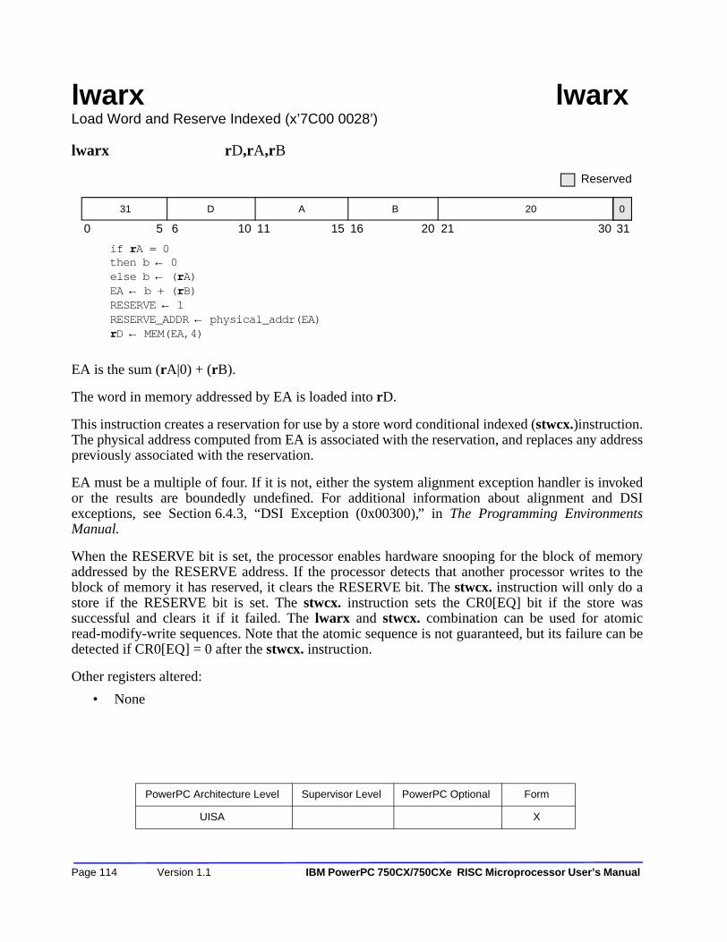
lwarx lwarxLoad Word and Reserve Indexed (x’7C00 0028’)
lwarx rD,rA,rB
if rA = 0 then b ← 0else b ← (rA)EA ← b + (rB)RESERVE ← 1RESERVE_ADDR ← physical_addr(EA)rD ← MEM(EA,4)
EA is the sum (rA|0) + (rB).
The word in memory addressed by EA is loaded into rD.
This instruction creates a reservation for use by a store word conditional indexed (stwcx.)instruction.The physical address computed from EA is associated with the reservation, and replaces any addresspreviously associated with the reservation.
EA must be a multiple of four. If it is not, either the system alignment exception handler is invokedor the results are boundedly undefined. For additional information about alignment and DSIexceptions, see Section 6.4.3, “DSI Exception (0x00300),” in The Programming EnvironmentsManual.
When the RESERVE bit is set, the processor enables hardware snooping for the block of memoryaddressed by the RESERVE address. If the processor detects that another processor writes to theblock of memory it has reserved, it clears the RESERVE bit. The stwcx. instruction will only do astore if the RESERVE bit is set. The stwcx. instruction sets the CR0[EQ] bit if the store wassuccessful and clears it if it failed. The lwarx and stwcx. combination can be used for atomicread-modify-write sequences. Note that the atomic sequence is not guaranteed, but its failure can bedetected if CR0[EQ] = 0 after the stwcx. instruction.
Other registers altered:
• None
0 5 6 10 11 15 16 20 21 30 31
Reserved
B 20 031 D A
PowerPC Architecture Level Supervisor Level PowerPC Optional Form
UISA X
P
age 114 Version 1.1 IBM PowerPC 750CX/750CXe RISC Microprocessor U ser’s Manual
lwbrx lwbrxLoad Word Byte-Reverse Indexed (x’7C00 042C’)
lwbrx rD,rA,rB
if rA = 0 then b ← 0else b ← (rA)EA ← b + (rB)rD ← MEM(EA + 3, 1) || MEM(EA + 2, 1) || MEM(EA + 1, 1) || MEM(EA, 1)
EA is the sum (rA|0) + rB. Bits 0–7 of the word in memory addressed by EA are loaded into thelow-order 8 bits of rD. Bits 8–15 of the word in memory addressed by EA are loaded into thesubsequent low-order 8 bits of rD. Bits 16–23 of the word in memory addressed by EA are loadedinto the subsequent low-order eight bits of rD. Bits 24–31 of the word in memory addressed by EAare loaded into the subsequent low-order 8 bits of rD.
The PowerPC architecture cautions programmers that some implementations of the architecture mayrun the lwbrx instructions with greater latency than other types of load instructions.
Other registers altered:
• None
0 5 6 10 11 15 16 20 21 30 31
Reserved
B 534 031 D A
PowerPC Architecture Level Supervisor Level PowerPC Optional Form
UISA X
T
able of Contents 5/9/02 Page 115
lwz lwzLoad Word and Zero (x’8000 0000’)
lwz rD,d(rA)
if rA = 0 then b ← 0else b ← (rA)EA ← b + EXTS(d)rD ← MEM(EA, 4)
EA is the sum (rA|0) + d. The word in memory addressed by EA is loaded into rD.
Other registers altered:
• None
0 5 6 10 11 15 16 31
d32 D A
PowerPC Architecture Level Supervisor Level PowerPC Optional Form
UISA D
P
age 116 Version 1.1 IBM PowerPC 750CX/750CXe RISC Microprocessor User’s Manual
lwzu lwzuLoad Word and Zero with Update (x’8400 0000’)
lwzu rD,d(rA)
EA ← rA + EXTS(d)rD ← MEM(EA, 4)rA ← EA
EA is the sum (rA) + d. The word in memory addressed by EA is loaded into rD.
EA is placed into rA.
If rA = 0, or rA = rD, the instruction form is invalid.
Other registers altered:
• None
0 5 6 10 11 15 16 31
d33 D A
PowerPC Architecture Level Supervisor Level PowerPC Optional Form
UISA D
T
able of Contents 5/9/02 Page 117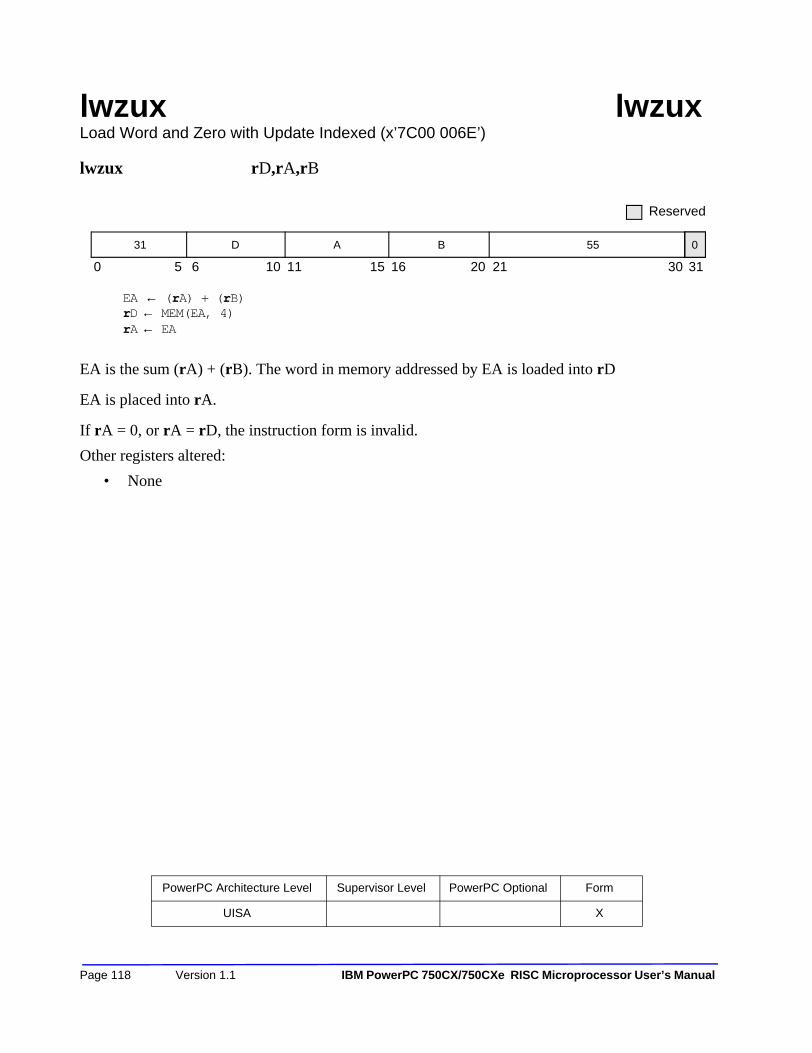
lwzux lwzuxLoad Word and Zero with Update Indexed (x’7C00 006E’)
lwzux rD,rA,rB
EA ← (rA) + (rB)rD ← MEM(EA, 4)rA ← EA
EA is the sum (rA) + (rB). The word in memory addressed by EA is loaded into rD
EA is placed into rA.
If rA = 0, or rA = rD, the instruction form is invalid.
Other registers altered:
• None
0 5 6 10 11 15 16 20 21 30 31
Reserved
B 55 031 D A
PowerPC Architecture Level Supervisor Level PowerPC Optional Form
UISA X
P
age 118 Version 1.1 IBM PowerPC 750CX/750CXe RISC Microprocessor U ser’s Manual
lwzx lwzxLoad Word and Zero Indexed (x’7C00 002E’)
lwzx rD,rA,rB
if rA = 0 then b ← 0else b ← (rA)EA ← b + rBrD ← MEM(EA, 4)
EA is the sum (rA|0) + (rB). The word in memory addressed by EA is loaded into rD.
Other registers altered:
• None
0 5 6 10 11 15 16 20 21 30 31
Reserved
B 23 031 D A
PowerPC Architecture Level Supervisor Level PowerPC Optional Form
UISA X
T
able of Contents 5/9/02 Page 119
mcrf mcrfMove Condition Register Field (x’4C00 0000’)
mcrf crfD,crfS
CR[4 ∗ crfD–4 ∗ crfD + 3] ← CR[4 ∗ crfS–4 ∗ crfS + 3]
The contents of condition register field crfS are copied into condition register field crfD. All othercondition register fields remain unchanged.
Other registers altered:
• Condition Register (CR field specified by operand crfD)
Affected: LT, GT, EQ, SO
0 5 6 8 9 10 11 13 14 15 16 20 21 30 31
Reserved
19 crfD 0 0 crfS 0 0 0 0 0 0 0 0 0 0 0 0 0 0 0 0 0 0
PowerPC Architecture Level Supervisor Level PowerPC Optional Form
UISA XL
P
age 120 Version 1.1 IBM PowerPC 750CX/750CXe RISC Microprocessor U ser’s Manual
mcrfs mcrfsMove to Condition Register from FPSCR (x’FC00 0080’)
mcrfs crfD,crfS
The contents of FPSCR field crfS are copied to CR field crfD. All exception bits copied (except FEXand VX) are cleared in the FPSCR.
Other registers altered:
• Condition Register (CR field specified by operand crfD)
Affected: FX, FEX, VX, OX
• Floating-Point Status and Control Register
Affected: FX, OX (if crfS = 0)
Affected: UX, ZX, XX, VXSNAN (if crfS = 1)
Affected: VXISI, VXIDI, VXZDZ, VXIMZ (if crfS = 2)
Affected: VXVC (if crfS = 3)
Affected: VXSOFT, VXSQRT, VXCVI (if crfS = 5)
0 5 6 8 9 10 11 13 14 15 16 20 21 30 31
Reserved
63 crfD 0 0 crfS 0 0 0 0 0 0 0 64 0
PowerPC Architecture Level Supervisor Level PowerPC Optional Form
UISA X
T
able of Contents 5/9/02 Page 121
mcrxr mcrxrMove to Condition Register from XER (x’7C00 0400’)
mcrxr crfD
CR[4 ∗ crfD , 4 ∗ crfD + 3] ← XER[0–3]XER[0–3] ← 0b0000
The contents of XER[0–3] are copied into the condition register field designated by crfD. All otherfields of the condition register remain unchanged. XER[0–3] is cleared.
Other registers altered:
• Condition Register (CR field specified by operand crfD)
Affected: LT, GT, EQ, SO
• XER[0–3]
0 5 6 8 9 10 11 15 16 20 21 30 31
Reserved
31 crfD 0 0 0 0 0 0 0 0 0 0 0 0 512 0
PowerPC Architecture Level Supervisor Level PowerPC Optional Form
UISA X
P
age 122 Version 1.1 IBM PowerPC 750CX/750CXe RISC Microprocessor U ser’s Manual
mfcr mfcr Move from Condition Register (x’7C00 0026’)
mfcr rD
rD ← CR
The contents of the condition register (CR) are placed into rD.
Other registers altered:
• None
0 5 6 10 11 15 16 20 21 30 31
Reserved
0 0 0 0 0 19 031 D 0 0 0 0 0
PowerPC Architecture Level Supervisor Level PowerPC Optional Form
UISA X
T
able of Contents 5/9/02 Page 123
Page 124 Version 1.1 IBM PowerPC 750CX/750CXe RISC Microprocessor User’s Manual

mffsx mffsx Move from FPSCR (x’FC00 048E’)
mffs frD (Rc = 0)mffs. frD (Rc = 1)
frD[32-63] ← FPSCR
The contents of the floating-point status and control register (FPSCR) are placed into the low-orderbits of register frD. The high-order bits of register frD are undefined.
Other registers altered:
• Condition Register (CR1 field)
Affected: FX, FEX, VX, OX (if Rc = 1)
0 5 6 10 11 15 16 20 21 30 31
Reserved
0 0 0 0 0 583 Rc63 D 0 0 0 0 0
PowerPC Architecture Level Supervisor Level PowerPC Optional Form
UISA X
T
able of Contents 5/9/02 Page 125
mfmsr mfmsr Move from Machine State Register (x’7C00 00A6’)
mfmsr rD
rD ← MSR
The contents of the MSR are placed into rD.
This is a supervisor-level instruction.
Other registers altered:
• None
0 5 6 10 11 15 16 20 21 30 31
Reserved
0 0 0 0 0 83 031 D 0 0 0 0 0
PowerPC Architecture Level Supervisor Level PowerPC Optional Form
OEA Yes X
P
age 126 Version 1.1 IBM PowerPC 750CX/750CXe RISC Microprocessor U ser’s Manual
mfspr mfspr Move from Special-Purpose Register (x’7C00 02A6’)
mfspr rD,SPR
n ← spr[5–9] || spr[0–4]rD ← SPR(n)
In the PowerPC UISA, the SPR field denotes a special-purpose register, encoded as shown inTable 12-9. The contents of the designated special purpose register are placed into rD.
If the SPR field contains any value other than one of the values shown in Table 12-9 (and theprocessor is in user mode), one of the following occurs:
• The system illegal instruction error handler is invoked.
• The system supervisor-level instruction error handler is invoked.
• The results are boundedly undefined.
Other registers altered:
• None
Simplified mnemonics:
mfxerrD equivalent tomfspr rD,1mflr rD equivalent tomfspr rD,8mfctrrD equivalent tomfspr rD,9
Table 12-9. PowerPC 750CX UISA SPR Encodings for mfspr
SPR**Register Name
Decimal spr[5–9] spr[0–4]
1 00000 00001 XER
8 00000 01000 LR
9 00000 01001 CTR
** Note that the order of the two 5-bit halves of the SPR number is reversed compared with the actual instruction coding.
0 5 6 10 11 20 21 30 31
Reserved
spr* 339 031 D
*Note: This is a split field.
T
able of Contents 5/9/02 Page 127
In the PowerPC OEA, the SPR field denotes a special-purpose register, encoded as shown inTable 12-10. The contents of the designated SPR are placed into rD.
In the PowerPC UISA, the SPR field denotes a special-purpose register, encoded as shown inTable 12-10. If the SPR[0] = 0 (Access type User), the contents of the designated SPR are placed intorD.
SPR[0] = 1 if and only if reading the register is supervisor-level. Execution of this instructionspecifying a defined and supervisor-level register when MSR[PR] = 1 will result in a privilegedinstruction type program exception.
If MSR[PR] = 1, the only effect of executing an instruction with an SPR number that is not shown inTable 12-10 and has SPR[0] = 1 is to cause a supervisor-level instruction type program exception oran illegal instruction type program exception. For all other cases, MSR[PR] = 0 or SPR[0] = 0.
If the SPR field contains any value that is not shown in Table 12-10, either an illegal instruction typeprogram exception occurs or the results are boundedly undefined.
Table 12-10. PowerPC 750CX OEA SPR Encodings for mfspr SPR
1
Register Name AccessDecimal spr[5–9] spr[0–4]
1 00000 00001 XER User
8 00000 01000 LR User9 00000 01001 CTR User
18 00000 10010 DSISR Supervisor
19 00000 10011 DAR Supervisor22 00000 10110 DEC Supervisor
25 00000 11001 SDR1 Supervisor
26 00000 11010 SRR0 Supervisor27 00000 11011 SRR1 Supervisor
272 01000 10000 SPRG0 Supervisor
273 01000 10001 SPRG1 Supervisor274 01000 10010 SPRG2 Supervisor
275 01000 10011 SPRG3 Supervisor
282 01000 11010 EAR Supervisor287 01000 11111 PVR Supervisor
528 10000 10000 IBAT0U Supervisor
529 10000 10001 IBAT0L Supervisor530 10000 10010 IBAT1U Supervisor
531 10000 10011 IBAT1L Supervisor
532 10000 10100 IBAT2U Supervisor533 10000 10101 IBAT2L Supervisor
534 10000 10110 IBAT3U Supervisor
535 10000 10111 IBAT3L Supervisor536 10000 11000 DBAT0U Supervisor
537 10000 11001 DBAT0L Supervisor
538 10000 11010 DBAT1U Supervisor539 10000 11011 DBAT1L Supervisor
540 10000 11100 DBAT2U Supervisor
Page 128 Version 1.1 IBM PowerPC 750CX/750CXe RISC Microprocessor User’s Manual

541 10000 11101 DBAT2L Supervisor
542 10000 11110 DBAT3U Supervisor
543 10000 11111 DBAT3L Supervisor936 11101 01000 UMMCR0 User
937 11101 01001 UPMC1 User
938 11101 01010 UPMC2 User939 11101 01011 USIA User
940 11101 01100 UMMCR1 User
941 11101 01101 UPMC3 User942 11101 01110 UPMC4 User
943 11101 01111 USDA User
952 11101 11000 MMCR0 Supervisor953 11101 11001 PMC1 Supervisor
954 11101 11010 PMC2 Supervisor
955 11101 11011 SIA Supervisor
956 11101 11100 MMCR1 Supervisor957 11101 11101 PMC3 Supervisor
958 11101 11110 PMC4 Supervisor
959 11101 11111 SDA Supervisor1008 11111 10000 HID0 Supervisor
1009 11111 10001 HID1 Supervisor
1010 11111 10010 IABR Supervisor1013 11111 10101 DABR Supervisor
1017 11111 11001 L2CR Supervisor
1019 11111 11011 ICTC Supervisor1020 11111 11100 THRM1 Supervisor
1021 11111 11101 THRM2 Supervisor
1022 11111 11110 THRM3 Supervisor1Note that the order of the two 5-bit halves of the SPR number is reversed compared with actual instruction coding.
For mtspr and mfspr instructions, the SPR number coded in assembly language does not appear directly as a 10-bit binary number in the instruction. The number coded is split into two 5-bit halves that are reversed in the instruction, with the high-order five bits appearing in bits 16–20 of the instruction and the low-order five bits in bits 11–15.
* Note that mfspr is supervisor-level only if SPR[0] = 1.
Table 12-10. PowerPC 750CX OEA SPR Encodings for mfspr (Continued) SPR
1
Register Name AccessDecimal spr[5–9] spr[0–4]
PowerPC Architecture Level Supervisor Level PowerPC Optional Form
UISA/OEA Yes* XFX
T
able of Contents 5/9/02 Page 129
mfsr mfsr Move from Segment Register (x’7C00 04A6’)
mfsr rD,SR
rD ← SEGREG(SR)
The contents of the segment register SR are copied into rD.
This is a supervisor-level instruction.
Other registers altered:
• None
0 5 6 10 11 12 15 16 20 21 30 31
Reserved
0 0 0 0 0 595 031 D 0 SR
PowerPC Architecture Level Supervisor Level PowerPC Optional Form
OEA Yes X
P
age 130 Version 1.1 IBM PowerPC 750CX/750CXe RISC Microprocessor U ser’s Manual
mfsrin mfsrin Move from Segment Register Indirect (x’7C00 0526’)
mfsrin rD,rB
rD ← SEGREG(SR)
The contents of the segment register selected by bits 0–3 of rB are copied into rD.
This is a supervisor-level instruction.
NOTE: The rA field is not defined for the mfsrin instruction in the PowerPC architecture. However, mfsrin performs the same function in the PowerPC architecture as does the mfsri instruction in the POWER architecture (if rA = 0).
Other registers altered:
• None
0 5 6 10 11 12 15 16 20 21 30 31
Reserved
0 0 0 0 0 595 031 D 0 SR
PowerPC Architecture Level Supervisor Level PowerPC Optional Form
OEA Yes X
T
able of Contents 5/9/02 Page 131
mftb mftb Move from Time Base (x’7C00 02E6’)
mftb rD,TBR
n ← tbr[5–9] || tbr[0–4]if n = 268 then rD ← TBLelse if n = 269
then rD ← TBUelse error(invalid TBR field)
The contents of TBL or TBU are copied into rD, as designated by the value in TBR, encoded as shownhere.
If the TBR field contains any value other than one of the values shown in Table 12-11, then one of thefollowing occurs:
• The system illegal instruction error handler is invoked.
• The system supervisor-level instruction error handler is invoked.
• The results are boundedly undefined.
Important Note: Some implementations may implement mftb and mfspr identically, therefore, aTBR number should not match an SPR number.
For more information on the time base refer to Section 2.2, “PowerPC VEA Register Set—TimeBase,” in the PowerPC Microprocessor Family: The Programming Environments manual.
Other registers altered:
• None
Table 12-11. TBR Encodings for mftb
TBR* RegisterName
AccessDecimal tbr[5–9] tbr[0–4]
268 01000 01100 TBL User
269 01000 01101 TBU User
*Note that the order of the two 5-bit halves of the TBR number is reversed.
0 5 6 10 11 20 21 30 31
Reserved
31 D tbr* 371 0
*Note: This is a split field.
P
age 132 Version 1.1 IBM PowerPC 750CX/750CXe RISC Microprocessor U ser’s Manual
Simplified mnemonics:
mftb rD equivalent tomftb rD,268mftburD equivalent tomftb rD,269
PowerPC Architecture Level Supervisor Level PowerPC Optional Form
VEA XFX
T
able of Contents 5/9/02 Page 133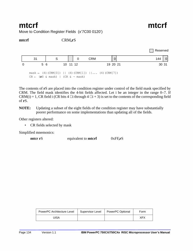
mtcrf mtcrf Move to Condition Register Fields (x’7C00 0120’)
mtcrf CRM,rS
mask ← (4)(CRM[0]) || (4)(CRM[1]) ||... (4)(CRM[7])CR ← (rS & mask) | (CR & ¬ mask)
The contents of rS are placed into the condition register under control of the field mask specified byCRM. The field mask identifies the 4-bit fields affected. Let i be an integer in the range 0–7. IfCRM(i) = 1, CR field i (CR bits 4 ∗ i through 4 ∗ i + 3) is set to the contents of the corresponding fieldof rS.
NOTE: Updating a subset of the eight fields of the condition register may have substantially poorer performance on some implementations than updating all of the fields.
Other registers altered:
• CR fields selected by mask
Simplified mnemonics:
mtcr rS equivalent to mtcrf 0xFF,rS
0 5 6 10 11 12 19 20 21 30 31
Reserved
CRM 0 144 031 S 0
PowerPC Architecture Level Supervisor Level PowerPC Optional Form
UISA XFX
P
age 134 Version 1.1 IBM PowerPC 750CX/750CXe RISC Microprocessor U ser’s Manual
mtfsb0x mtfsb0xMove to FPSCR Bit 0 (x’FC00 008C’)
mtfsb0 crbD (Rc = 0)mtfsb0. crbD (Rc = 1)
FPSRC(crbD)← 0
Bit crbD of the FPSCR is cleared.
Other registers altered:
• Condition Register (CR1 field)
Affected: FX, FEX, VX, OX(if Rc = 1)
• Floating-Point Status and Control Register
Affected: FPSCR bit crbD
NOTE: Bits 1 and 2 (FEX and VX) cannot be explicitly cleared.
0 5 6 10 11 15 16 20 21 30 31
Reserved
0 0 0 0 0 70 Rc63 crbD 0 0 0 0 0
PowerPC Architecture Level Supervisor Level PowerPC Optional Form
UISA X
T
able of Contents 5/9/02 Page 135
mtfsb1x mtfsb1x Move to FPSCR Bit 1 (x’FC00 004C’)
mtfsb1 crbD (Rc = 0)mtfsb1. crbD (Rc = 1)
FPSRC(crbD)← 1
Bit crbD of the FPSCR is set.
Other registers altered:
• Condition Register (CR1 field)
Affected: FX, FEX, VX, OX(if Rc = 1)
• Floating-Point Status and Control Register
Affected: FPSCR bit crbD and FX
NOTE: Bits 1 and 2 (FEX and VX) cannot be explicitly set.
0 5 6 10 11 15 16 20 21 30 31
Reserved
0 0 0 0 0 38 Rc63 crbD 0 0 0 0 0
PowerPC Architecture Level Supervisor Level PowerPC Optional Form
UISA X
P
age 136 Version 1.1 IBM PowerPC 750CX/750CXe RISC Microprocessor U ser’s Manual
mtfsfx mtfsfxMove to FPSCR Fields (x’FC00 058E’)
mtfsf FM,frB (Rc = 0)mtfsf. FM,frB (Rc = 1)
The low-order 32 bits of frB are placed into the FPSCR under control of the field mask specified byFM. The field mask identifies the 4-bit fields affected. Let i be an integer in the range 0–7. If FM[i]= 1, FPSCR field i (FPSCR bits 4 * i through 4 * i + 3) is set to the contents of the corresponding fieldof the low-order 32 bits of register frB.
FPSCR[FX] is altered only if FM[0] = 1.
Updating fewer than all eight fields of the FPSCR may have substantially poorer performance onsome implementations than updating all the fields.
When FPSCR[0–3] is specified, bits 0 (FX) and 3 (OX) are set to the values of frB[32] and frB[35](that is, even if this instruction causes OX to change from 0 to 1, FX is set from frB[32] and not bythe usual rule that FX is set when an exception bit changes from 0 to 1). Bits 1 and 2 (FEX and VX)are set according to the usual rule and not from frB[33–34].
Other registers altered:
• Condition Register (CR1 field)
Affected: FX, FEX, VX, OX (if Rc = 1)
• Floating-Point Status and Control Register
Affected: FPSCR fields selected by mask
0 5 6 7 14 15 16 20 21 30 31
Reserved
63 0 FM 0 B 711 Rc
PowerPC Architecture Level Supervisor Level PowerPC Optional Form
UISA XFL
T
able of Contents 5/9/02 Page 137
mtfsfix mtfsfix
Move to FPSCR Field Immediate (x’FC00 010C’)
mtfsfi crfD,IMM (Rc = 0)mtfsfi. crfD,IMM (Rc = 1)
FPSCR[crfD] ← IMM
The value of the IMM field is placed into FPSCR field crfD.
FPSCR[FX] is altered only if crfD = 0.
When FPSCR[0–3] is specified, bits 0 (FX) and 3 (OX) are set to the values of IMM[0] and IMM[3](that is, even if this instruction causes OX to change from 0 to 1, FX is set from IMM[0] and not bythe usual rule that FX is set when an exception bit changes from 0 to 1). Bits 1 and 2 (FEX and VX)are set according to the usual rule and not from IMM[1–2].
Other registers altered:
• Condition Register (CR1 field)
Affected: FX, FEX, VX, OX (if Rc = 1)
• Floating-Point Status and Control Register
Affected: FPSCR field crfD
0 5 6 8 9 10 1112 15 16 19 20 21 30 31
Reserved
63 crfD 0 0 0 0 0 0 0 IMM 0 134
PowerPC Architecture Level Supervisor Level PowerPC Optional Form
UISA X
P
age 138 Version 1.1 IBM PowerPC 750CX/750CXe RISC Microprocessor U ser’s Manual
mtmsr mtmsr Move to Machine State Register (x’7C00 0124’)
mtmsr rS
MSR ← (rS)
The contents of rS are placed into the MSR.
This is a supervisor-level instruction. It is also an execution synchronizing instruction except withrespect to alterations to the POW and LE bits. Refer to Section 2.3.18, “SynchronizationRequirements for Special Registers and for Lookaside Buffers” in the the PowerPC MicroprocessorFamily: The Programming Environments manual for more information.
In addition, alterations to the MSR[EE] and MSR[RI] bits are effective as soon as the instructioncompletes. Thus if MSR[EE] = 0 and an external or decrementer exception is pending, executing anmtmsr instruction that sets MSR[EE] = 1 will cause the external or decrementer exception to be takenbefore the next instruction is executed, if no higher priority exception exists.
Other registers altered:
• MSR
0 5 6 10 11 15 16 20 21 30 31
Reserved
0 0 0 0 0 146 031 S 0 0 0 0 0
PowerPC Architecture Level Supervisor Level PowerPC Optional Form
OEA Yes X
T
able of Contents 5/9/02 Page 139
mtspr mtsprMove to Special-Purpose Register (x’7C00 03A6’)
mtspr SPR,rS
n ← spr[5–9] || spr[0–4]
In the PowerPC UISA, the SPR field denotes a special-purpose register, encoded as shown inTable 12-12. The contents of rS are placed into the designated special-purpose register
If the SPR field contains any value other than one of the values shown in Table 12-12, and theprocessor is operating in user mode, one of the following occurs:
• The system illegal instruction error handler is invoked.
• The system supervisor instruction error handler is invoked.
• The results are boundedly undefined.
Simplified mnemonics:
mtxerrD equivalent tomtspr 1,rDmtlr rD equivalent tomtspr 8,rDmtctrrD equivalent tomtspr 9,rD
In the PowerPC OEA, the SPR field denotes a special-purpose register, encoded as shown inTable 12-13. The contents of rS are placed into the designated special-purpose register.
In the PowerPC UISA, if the SPR[0]=0 (Access is User) the contents of rS are placed into thedesignated special-purpose register
For this instruction, SPRs TBL and TBU are treated as separate 32-bit registers; setting one leaves theother unaltered.
Table 12-12. PowerPC 750CX UISA SPR Encodings for mtspr
SPR**Register Name
Decimal spr[5–9] spr[0–4]
1 00000 00001 XER
8 00000 01000 LR
9 00000 01001 CTR
** Note that the order of the two 5-bit halves of the SPR number is reversed compared with actual instruction coding.
0 5 6 10 11 20 21 30 31
Reserved
spr* 467 031 S
*Note: This is a split field.
P
age 140 Version 1.1 IBM PowerPC 750CX/750CXe RISC Microprocessor U ser’s Manual
The value of SPR[0] = 1 if and only if writing the register is a supervisor-level operation. Executionof this instruction specifying a defined and supervisor-level register when MSR[PR] = 1 results in aprivileged instruction type program exception.
If MSR[PR] = 1 then the only effect of executing an instruction with an SPR number that is not shownin Table 12-13 and has SPR[0] = 1 is to cause a privileged instruction type program exception or anillegal instruction type program exception. For all other cases, MSR[PR] = 0 or SPR[0] = 0, if theSPR field contains any value that is not shown in Table 12-13, either an illegal instruction typeprogram exception occurs or the results are boundedly undefined.
Other registers altered:
• See Table 12-13.
Table 12-13. PowerPC 750CX OEA SPR Encodings for mtspr
SPR1
Register Name AccessDecimal spr[5–9] spr[0–4]
1 00000 00001 XER User
8 00000 01000 LR User
9 00000 01001 CTR User
18 00000 10010 DSISR Supervisor
19 00000 10011 DAR Supervisor
22 00000 10110 DEC Supervisor
25 00000 11001 SDR1 Supervisor
26 00000 11010 SRR0 Supervisor
27 00000 11011 SRR1 Supervisor
272 01000 10000 SPRG0 Supervisor
273 01000 10001 SPRG1 Supervisor
274 01000 10010 SPRG2 Supervisor
275 01000 10011 SPRG3 Supervisor
282 01000 11010 EAR Supervisor
284 01000 11100 TBL Supervisor
285 01000 11101 TBU Supervisor
528 10000 10000 IBAT0U Supervisor
529 10000 10001 IBAT0L Supervisor
530 10000 10010 IBAT1U Supervisor
531 10000 10011 IBAT1L Supervisor
532 10000 10100 IBAT2U Supervisor
533 10000 10101 IBAT2L Supervisor
534 10000 10110 IBAT3U Supervisor
535 10000 10111 IBAT3L Supervisor
536 10000 11000 DBAT0U Supervisor
537 10000 11001 DBAT0L Supervisor
538 10000 11010 DBAT1U Supervisor
Table of Contents 5/9/02 Page 141

539 10000 11011 DBAT1L Supervisor
540 10000 11100 DBAT2U Supervisor
541 10000 11101 DBAT2L Supervisor
542 10000 11110 DBAT3U Supervisor
543 10000 11111 DBAT3L Supervisor
936 11101 01000 UMMCR0 User
937 11101 01001 UPMC1 User
938 11101 01010 UPMC2 User
939 11101 01011 USIA User
940 11101 01100 UMMCR1 User
941 11101 01101 UPMC3 User
942 11101 01110 UPMC4 User
943 11101 01111 USDA User
952 11101 11000 MMCR0 Supervisor
953 11101 11001 PMC1 Supervisor
954 11101 11010 PMC2 Supervisor
955 11101 11011 SIA Supervisor
956 11101 11100 MMCR1 Supervisor
957 11101 11101 PMC3 Supervisor
958 11101 11110 PMC4 Supervisor
959 11101 11111 SDA Supervisor
1008 11111 10000 HID0 Supervisor
1009 11111 10001 HID1 Supervisor
1010 11111 10010 IABR Supervisor
1013 11111 10101 DABR Supervisor
1017 11111 11001 L2CR Supervisor
1019 11111 11011 ICTC Supervisor
1020 11111 11100 THRM1 Supervisor
1021 11111 11101 THRM2 Supervisor
1022 11111 11110 THRM3 Supervisor
1Note that the order of the two 5-bit halves of the SPR number is reversed. For mtspr and mfspr instructions, the SPR number coded in assembly language does not appear directly as a 10-bit binary number in the instruction. The number coded is split into two 5-bit halves that are reversed in the instruction, with the high-order five bits appearing in bits 16–20 of the instruction and the low-order five bits in bits 11–15.
Note: mfspr is supervisor-level only if SPR[0] = 1.
Table 12-13. PowerPC 750CX OEA SPR Encodings for mtspr (Continued)
SPR1
Register Name AccessDecimal spr[5–9] spr[0–4]
PowerPC Architecture Level Supervisor Level PowerPC Optional Form
OEA Yes XFX
P
age 142 Version 1.1 IBM PowerPC 750CX/750CXe RISC Microprocessor User’s Manual
mtsr mtsrMove to Segment Register (x’7C00 01A4’)
mtsr SR,rS
SEGREG(SR) ← (rS)
The contents of rS are placed into SR.
This is a supervisor-level instruction.
Other registers altered:
• None
0 5 6 10 11 12 15 16 20 21 30 31
Reserved
0 0 0 0 0 210 031 S 0
PowerPC Architecture Level Supervisor Level PowerPC Optional Form
OEA Yes X
T
able of Contents 5/9/02 Page 143
mtsrin mtsrin Move to Segment Register Indirect (x’7C00 01E4’)
mtsrin rS,rB
SEGREG(rB[0–3]) ← (rS)
The contents of rS are copied to the segment register selected by bits 0–3 of rB.
This is a supervisor-level instruction.
NOTE: The PowerPC architecture does not define the rA field for the mtsrin instruction. However, mtsrin performs the same function in the PowerPC architecture as does the mtsri instruction in the POWER architecture (if rA = 0).
Other registers altered:
• None
0 5 6 10 11 15 16 20 21 30 31
Reserved
B 242 031 S 0 0 0 0 0
PowerPC Architecture Level Supervisor Level PowerPC Optional Form
OEA Yes X
P
age 144 Version 1.1 IBM PowerPC 750CX/750CXe RISC Microprocessor U ser’s Manual
mulhwx mulhwx Multiply High Word (x’7C00 0096’)
mulhw rD,rA,rB (Rc = 0)mulhw. rD,rA,rB (Rc = 1)
prod[0–63] ← (rA ∗ (rBrD ← prod
The 32-bit product is formed from the contents rA and rB. The high-order 32 bits of the 64-bitproduct of the operands are placed into rD. Both the operands and the product are interpreted assigned integers.
This instruction may execute faster on some implementations if rB contains the operand having thesmaller absolute value.
Other registers altered:
• Condition Register (CR0 field)
Affected: LT, GT, EQ, SO (if Rc = 1)
Reserved
0 5 6 10 11 15 16 20 21 22 30 31
31 D A B 0 75 Rc
PowerPC Architecture Level Supervisor Level PowerPC Optional Form
UISA XO
Table of Contents 5/9/02
Page 145
mulhwux mulhwux Multiply High Word Unsigned (x’7C00 0016’)
mulhwu rD,rA,rB (Rc = 0)mulhwu. rD,rA,rB (Rc = 1)
prod[0–63] ← (rA) ∗ (rBrD ← prod[0–31]]
The 32-bit operands are the contents rA and rB. The high-order 32 bits of the 64-bit product of theoperands are placed into rD.
Both the operands and the product are interpreted as unsigned integers, except that if Rc = 1 the first three bits of CR0 field are set by signed comparison of the result to zero.
This instruction may execute faster on some implementations if rB contains the operand having thesmaller absolute value.
Other registers altered:
• Condition Register (CR0 field)
Affected: LT, GT, EQ, SO (if Rc = 1)
Reserved
0 5 6 10 11 15 16 20 21 22 30 31
31 D A B 0 11 Rc
PowerPC Architecture Level Supervisor Level PowerPC Optional Form
UISA XO
Page 146 Version 1.1 IBM PowerPC 750CX/750CXe RISC Microprocessor U
ser’s Manual
mulli mulli Multiply Low Immediate (x’1C00 0000’)
mulli rD,rA,SIMM
prod[0–48] ← (rA) ∗ SIMMrD ← prod[16-48]
The first operand is rA. The second operand is the value of the SIMM field. The low-order 32-bits ofthe 48-bit product of the operands are placed into rD.
Both the operands and the product are interpreted as signed integers. The low-order of the product arecalculated independently of whether the operands are treated as signed or unsigned 32-bit integers.
This instruction can be used with mulhdx or mulhwx to calculate a full 64-bit product.
Other registers altered:
• None
0 5 6 10 11 15 16 31
SIMM07 D A
PowerPC Architecture Level Supervisor Level PowerPC Optional Form
UISA D
T
able of Contents 5/9/02 Page 147
mullwx mullwx Multiply Low Word (x’7C00 01D6’)
mullw rD,rA,rB (OE = 0 Rc = 0)mullw. rD,rA,rB (OE = 0 Rc = 1)mullwo rD,rA,rB (OE = 1 Rc = 0) mullwo. rD,rA,rB (OE = 1 Rc = 1)
prod[0–48] ← (rA) ∗ (rBrD ← prod[16-48]
The 32-bit operands are the contents of rA and rB. The low-order of the 64-bit product (rA) * (rB)are placed into rD.
The low-order 32-bits of the product are independent of whether the operands are regarded as signedor unsigned 32-bit integers.
If OE = 1, then OV is set if the product cannot be represented in 32 bits. Both the operands and theproduct are interpreted as signed integers.
NOTE: This instruction may execute faster on some implementations if rB contains the operand having the smaller absolute value.
Other registers altered:
• Condition Register (CR0 field)
Affected: LT, GT, EQ, SO (if Rc = 1)
NOTE: CR0 field may not reflect the infinitely precise result if overflow occurs (see XER below).
• XER
Affected: SO, OV (if OE = 1)
0 5 6 10 11 15 16 20 21 22 30 31
31 D A B OE 235 Rc
PowerPC Architecture Level Supervisor Level PowerPC Optional Form
UISA XO
P
age 148 Version 1.1 IBM PowerPC 750CX/750CXe RISC Microprocessor User’s Manual
nandx nandx NAND (x’7C00 03B8’)
nand rA,rS,rB (Rc = 0)nand. rA,rS,rB (Rc = 1)
rA ← ¬ ((rS) & (rB))
The contents of rS are ANDed with the contents of rB and the complemented result is placed into rA.
nand with rS = rB can be used to obtain the one's complement.
Other registers altered:
• Condition Register (CR0 field)
0 5 6 10 11 15 16 20 21 30 31
31 S A B 476 Rc
PowerPC Architecture Level Supervisor Level PowerPC Optional Form
UISA X
T
able of Contents 5/9/02 Page 149
negx negx Negate (x’7C00 00D0’)
neg rD,rA (OE = 0 Rc = 0)neg. rD,rA (OE = 0 Rc = 1)nego rD,rA (OE = 1 Rc = 0)nego. rD,rA (OE = 1 Rc = 1)
rD ← ¬ (rA) + 1
The value 1 is added to the complement of the value in rA, and the resulting two’s complement isplaced into rD.
If rA contains the most negative 32-bit number (0x8000_0000), the result is the most negative numberand if OE = 1, OV is set.
Other registers altered:
• Condition Register (CR0 field)
Affected: LT, GT, EQ, SO (if Rc = 1)
• XER
Affected: SO OV (if OE = 1)
Reserved
0 5 6 10 11 15 16 20 21 22 30 31
31 D A 0 0 0 0 0 OE 104 Rc
PowerPC Architecture Level Supervisor Level PowerPC Optional Form
UISA XO
Page 150 Version 1.1 IBM PowerPC 750CX/750CXe RISC Microprocessor U
ser’s Manual
norx norx NOR (x’7C00 00F8’)
nor rA,rS,rB (Rc = 0)nor. rA,rS,rB (Rc = 1)
rA ← ¬ ((rS) | (rB))
The contents of rS are ORed with the contents of rB and the complemented result is placed into rA.
nor with rS = rB can be used to obtain the one’s complement.
Other registers altered:
• Condition Register (CR0 field)
Affected: LT, GT, EQ, SO (if Rc = 1)
Simplified mnemonics:
not rD,rS equivalent tonor rA,rS,rS
0 5 6 10 11 15 16 20 21 30 31
31 S A B 124 Rc
PowerPC Architecture Level Supervisor Level PowerPC Optional Form
UISA X
T
able of Contents 5/9/02 Page 151
orx orx OR (x’7C00 0378’)
or rA,rS,rB (Rc = 0)or. rA,rS,rB (Rc = 1)
rA ← (rS) | (rB)
The contents of rS are ORed with the contents of rB and the result is placed into rA.
The example under simplified mnemonic mr demonstrates the use of the or instruction to moveregister contents.
Other registers altered:
• Condition Register (CR0 field)
Affected: LT, GT, EQ, SO (if Rc = 1)
Simplified mnemonics:
mr rA,rS equivalent toor rA,rS,rS
0 5 6 10 11 15 16 20 21 30 31
31 S A B 444 Rc
PowerPC Architecture Level Supervisor Level PowerPC Optional Form
UISA X
P
age 152 Version 1.1 IBM PowerPC 750CX/750CXe RISC Microprocessor User’s Manual
orcx orcx OR with Complement (x’7C00 0338’)
orc rA,rS,rB (Rc = 0) orc. rA,rS,rB (Rc = 1)
rA ← (rS) | ¬ (rB)
The contents of rS are ORed with the complement of the contents of rB and the result is placed intorA.
Other registers altered:
• Condition Register (CR0 field)
Affected: LT, GT, EQ, SO (if Rc = 1)
0 5 6 10 11 15 16 20 21 30 31
31 S A B 412 Rc
PowerPC Architecture Level Supervisor Level PowerPC Optional Form
UISA X
T
able of Contents 5/9/02 Page 153
ori ori OR Immediate (x’6000 0000’)
ori rA,rS,UIMM
rA ← (rS) | ((16)0 || UIMM)
The contents of rS are ORed with 0x0000 || UIMM and the result is placed into rA.
The preferred no-op (an instruction that does nothing) is ori 0,0,0.
Other registers altered:
• None
Simplified mnemonics:
nop equivalent toori 0,0,0
0 5 6 10 11 15 16 31
24 S A UIMM
PowerPC Architecture Level Supervisor Level PowerPC Optional Form
UISA D
P
age 154 Version 1.1 IBM PowerPC 750CX/750CXe RISC Microprocessor User’s Manual
oris orisOR Immediate Shifted (x’6400 0000’)
oris rA,rS,UIMM
rA ← (rS) | (UIMM || (16)0)
The contents of rS are ORed with UIMM || 0x0000 and the result is placed into rA.
Other registers altered:
• None
0 5 6 10 11 15 16 31
25 S A UIMM
PowerPC Architecture Level Supervisor Level PowerPC Optional Form
UISA D
T
able of Contents 5/9/02 Page 155
Page 156 Version 1.1 IBM PowerPC 750CX/750CXe RISC Microprocessor User’s Manual

rfi rfiReturn from Interrupt (x’4C00 0064’)
MSR[0,5-9,16–23, 25–27, 30–31] ← SRR1[0,5-9,16–23, 25–27, 30–31]MSR[13] ← b’0’NIA ←iea SRR0[0–29] || 0b00
Bits SRR1[0,5-9,16–23, 25–27, 30–31] are placed into the corresponding bits of the MSR. MSR[13]is set to 0. If the new MSR value does not enable any pending exceptions, then the next instruction isfetched, under control of the new MSR value, from the address SRR0[0–29] || 0b00. If the new MSRvalue enables one or more pending exceptions, the exception associated with the highest prioritypending exception is generated; in this case the value placed into SRR0 by the exception processingmechanism is the address of the instruction that would have been executed next had the exception notoccurred. Note that an implementation may define additional MSR bits, and in this case, may alsocause them to be saved to SRR1 from MSR on an exception and restored to MSR from SRR1 on anrfi.
This is a supervisor-level, context synchronizing instruction.
Other registers altered:
• MSR
0 0 0 0 0 00 000 50 0
Reserved
0 5 6 10 11 15 16 20 21 30 31
19 00 000
PowerPC Architecture Level Supervisor Level PowerPC Optional Form
OEA YES XL
Table of Contents
5/9/02 Page 157
rlwimix rlwimix Rotate Left Word Immediate then Mask Insert (x’5000 0000’)
rlwimi rA,rS,SH,MB,ME (Rc = 0)rlwimi. rA,rS,SH,MB,ME (Rc = 1)
n ← SHr ← ROTL(rS, n)m ← MASK(MB, ME)rA ← (r & m) | (rA & ¬ m)
The contents of rS are rotated left the number of bits specified by operand SH. A mask is generatedhaving 1 bits from bit MB through bit ME and 0 bits elsewhere. The rotated data is inserted into rAunder control of the generated mask.
NOTE: rlwimi can be used to copy a bit field of any length from register rS into the contents of rA. This field can start from any bit position in rS and be placed into any position in rA. The length of the field can range from 0 to 32 bits. The remaining bits in register rA remain unchanged.
• To copy byte_0 (bits 0-7) from rS into byte_3 (bits 24-31) of rA, set SH = 8, set MB = 24, and set ME = 31.
• In general, to copy an n-bit field that starts in bit position b in register rS into register rA starting a bit position c: set SH = 32 - c + b Mod(32), set MB = c, and set ME = (c + n) – 1 Mod(32).
Other registers altered:
• Condition Register (CR0 field)
Affected: LT, GT, EQ, SO (if Rc = 1)
Simplified mnemonics:
inslwi rA,rS,n,b equivalent to rlwimi rA,rS,32 – b,b,b + n – 1insrwi rA,rS,n,b (n > 0)equivalent to rlwimi rA,rS,32 – (b + n),b,(b + n) – 1
0 5 6 10 11 15 16 20 21 25 26 30 31
20 S A SH MB ME Rc
PowerPC Architecture Level Supervisor Level PowerPC Optional Form
UISA M
P
age 158 Version 1.1 IBM PowerPC 750CX/750CXe RISC Microprocessor User’s Manual
rlwinmx rlwinmx Rotate Left Word Immediate then AND with Mask (x’5400 0000’)
rlwinm rA,rS,SH,MB,ME (Rc = 0)rlwinm. rA,rS,SH,MB,ME (Rc = 1)
n ← SHr ← ROTL(rS, n)m ← MASK(MB, ME)rA ← r & m
The contents of rS are rotated left the number of bits specified by operand SH. A mask is generatedhaving 1 bits from bit MB through bit ME and 0 bits elsewhere. The rotated data is ANDed with thegenerated mask and the result is placed into rA.
NOTE: rlwinm can be used to extract, rotate, shift, and clear bit fields using the methods shown below:
• To extract an n-bit field, that starts at bit position b in rS, right-justified into rA (clearing the remaining 32 – n bits of rA), set SH = b + n, set MB = 32 – n, and set ME = 31.
• To extract an n-bit field, that starts at bit position b in rS, left-justified into rA (clearing the remaining 32 – n bits of rA), set SH = b, set MB = 0, and set ME = n – 1.
• To rotate the contents of a register left (or right) by n bits, set SH = n (32 – n), setMB = 0, and set ME = 31.
• To shift the contents of a register right by n bits, by setting SH = 32 – n, MB = n, and ME = 31.
It can also be used to clear the high-order b bits of a register and then shift the result left by n bits by setting SH = n, by setting MB = b – n, and by setting ME = 31 – n.
• To clear the low-order n bits of a register, by setting SH = 0, MB = 0, and ME = 31 – n.
Other registers altered:
• Condition Register (CR0 field)
Affected: LT, GT, EQ, SO (if Rc = 1)
0 5 6 10 11 15 16 20 21 25 26 30 31
21 S A SH MB ME Rc
T
able of Contents 5/9/02 Page 159
Simplified mnemonics:
extlwi rA,rS,n,b (n > 0) equivalent to rlwinm rA,rS,b,0,n – 1extrwi rA,rS,n,b (n > 0) equivalent to rlwinm rA,rS,b + n,32 – n,31rotlwi rA,rS,n equivalent to rlwinm rA,rS,n,0,31rotrwi rA,rS,n equivalent to rlwinm rA,rS,32 – n,0,31slwi rA,rS,n (n < 32) equivalent to rlwinm rA,rS,n,0,31–nsrwi rA,rS,n (n < 32) equivalent to rlwinm rA,rS,32 – n,n,31 clrlwi rA,rS,n (n < 32) equivalent to rlwinm rA,rS,0,n,31clrrwi rA,rS,n (n < 32) equivalent to rlwinm rA,rS,0,0,31 – nclrlslwi rA,rS,b,n (n ð b < 32) equivalent to rlwinm rA,rS,n,b – n,31 – n
PowerPC Architecture Level Supervisor Level PowerPC Optional Form
UISA M
P
age 160 Version 1.1 IBM PowerPC 750CX/750CXe RISC Microprocessor User’s Manual
rlwnmx rlwnmx Rotate Left Word then AND with Mask (x’5C00 0000’)
rlwnm rA,rS,rB,MB,ME (Rc = 0)rlwnm. rA,rS,rB,MB,ME (Rc = 1)
n ← rB[27-31]r ← ROTL(rS, n)m ← MASK(MB, ME)rA ← r & m
The contents of rS are rotated left the number of bits specified by the low-order five bits of rB. Amask is generated having 1 bits from bit MB through bit ME and 0 bits elsewhere. The rotated datais ANDed with the generated mask and the result is placed into rA.
NOTE: rlwnm can be used to extract and to rotate bit fields using one of these methods:
• To extract an n-bit field, that starts at variable bit position b in rS, right-justified into rA (clearing the remaining 32 – n bits of rA), set the low-order five bits of rB to b + n, set MB = 32 – n, and set ME = 31.
• To extract an n-bit field, that starts at variable bit position b in rS, left-justified into rA (clearing the remaining 32 – n bits of rA), set the low-order five bits of rB to b, set MB = 0, and set ME = n – 1.
• To rotate the contents of a register left (or right) by n bits, set the low-order five bits of rB to n (32 – n), set MB = 0, and set ME = 31.
Other registers altered:
• Condition Register (CR0 field)
Affected: LT, GT, EQ, SO (if Rc = 1)
Simplified mnemonics:
rotlwrA,rS,rB equivalent to rlwnm rA,rS,rB,0,31
0 5 6 10 11 15 16 20 21 25 26 30 31
23 S A B MB ME Rc
PowerPC Architecture Level Supervisor Level PowerPC Optional Form
UISA M
T
able of Contents 5/9/02 Page 161
sc scSystem Call (x’4400 0002’)
In the PowerPC UISA, the sc instruction calls the operating system to perform a service. Whencontrol is returned to the program that executed the system call, the content of the registers dependson the register conventions used by the program providing the system service.
This instruction is context synchronizing, as described in Section 4.1.5.1, “Context SynchronizingInstructions,” in the PowerPC Microprocessor Family: The Programming Environments manual.
Other registers altered:
• Dependent on the system service
In PowerPC OEA, the sc instruction does the following:
SRR0 ←iea CIA + 4SRR1[1-41-4, 10-151] ← 0SRR1[0,5-9, 16-23, 25-27, 30-31] ← MSR[0,5-9, 16-23, 25-27, 30-31]MSR ← new_value (see below)NIA ←iea base_ea + 0xC00 (see below)
The EA of the instruction following the sc instruction is placed into SRR0. Bits 0, 5-9,16-23, 25-27,and 30-31 of the MSR are placed into the corresponding bits of SRR1, and bits 1-4 and 10-15 of SRR1are set to undefined values.
NOTE: An implementation may define additional MSR bits, and in this case, may also cause them to be saved to SRR1 from MSR on an exception and restored to MSR from SRR1 on an rfi; then a system call exception is generated. The exception causes the MSR to be altered as described in Section 6.4, “Exception Definitions” in The Programming Environments Manual.
The exception causes the next instruction to be fetched from offset 0xC00 from the physical baseaddress determined by the new setting of MSR[IP].
Other registers altered:
• SRR0
• SRR1
• MSR
0 0 0 0 0 0 0 0 0 0 0 0 0 0 1 0
Reserved
0 5 6 10 11 15 16 29 30 31
17 0 0 0 0 0 0 0 0 0 0
PowerPC Architecture Level Supervisor Level PowerPC Optional Form
UISA/OEA SC
Page 162 Version 1.1
IBM PowerPC 750CX/750CXe RISC Microprocessor U ser’s Manual
slwx slwx Shift Left Word (x’7C00 0030’)
slw rA,rS,rB (Rc = 0)slw. rA,rS,rB (Rc = 1)
n ← rB[27-31]r ← ROTL(rS , n)if rB[26] = 0 then m ← MASK(0 , 31 – n)else m ← (32)0rA ← r & m
The contents of rS are shifted left the number of bits specified by the low-order five bits of rB. Bitsshifted out of position 0 are lost. Zeros are supplied to the vacated positions on the right. The 32-bitresult is placed into rA. However, shift amounts from 32 to 63 give a zero result.
Other registers altered:
• Condition Register (CR0 field)
Affected: LT, GT, EQ, SO (if Rc = 1)
0 5 6 10 11 15 16 20 21 30 31
31 S A B 24 Rc
PowerPC Architecture Level Supervisor Level PowerPC Optional Form
UISA X
T
able of Contents 5/9/02 Page 163
srawx srawx Shift Right Algebraic Word (x’7C00 0630’)
sraw rA,rS,rB (Rc = 0)sraw. rA,rS,rB (Rc = 1)
n ← rB[27-31]r ← ROTL(rS, 32– n)if rB[26] = 0 then m ← MASK(n, 31)else m ← (32)0S ← rS(0)rA ← r & m | (32)S & ¬ mXER[CA] ← S & (r & ¬ m[0-31] ≠ 0
The contents of rS are shifted right the number of bits specified by the low-order five bits of rB (shiftamounts between 0-31). Bits shifted out of position 31 are lost. Bit 0 of rS is replicated to fill thevacated positions on the left. The 32-bit result is placed into rA. XER[CA] is set if rS contains anegative number and any 1 bits are shifted out of position 31; otherwise XER[CA] is cleared. A shiftamount of zero causes rA to receive the 32 bits of rS, and XER[CA] to be cleared. However, shiftamounts from 32 to 63 give a result of 32 sign bits, and cause XER[CA] to receive the sign bit of rS.
NOTE: The sraw instruction, followed by addze, can be used to divide quickly by 2n.
Other registers altered:
• Condition Register (CR0 field)
Affected: LT, GT, EQ, SO (if Rc = 1)
• XER
Affected: CA
0 5 6 10 11 15 16 20 21 30 31
31 S A B 792 Rc
PowerPC Architecture Level Supervisor Level PowerPC Optional Form
UISA X
P
age 164 Version 1.1 IBM PowerPC 750CX/750CXe RISC Microprocessor User’s Manual
srawix srawix Shift Right Algebraic Word Immediate (x’7C00 0670’)
srawi rA,rS,SH (Rc = 0) srawi. rA,rS,SH (Rc = 1)
n ← SHr ← ROTL(rS, 32 – n)m← MASK(n, 31)S ← rS(0)rA ← r & m | (32)S & ¬ mXER[CA] ← S(0) & ((r & ¬ m) ≠ 0)
The contents of rS are shifted right SH bits. Bits shifted out of position 31 are lost. Bit 0 of rS isreplicated to fill the vacated positions on the left. The result is placed into rA. XER[CA] is set if the32 bits of rS contain a negative number and any 1 bits are shifted out of position 31; otherwiseXER[CA] is cleared. A shift amount of zero causes rA to receive the value of rS, and XER[CA] tobe cleared.
NOTE: The srawi instruction followed by addze instruction can be used to divide quickly by 2n.
Other registers altered:
• Condition Register (CR0 field)
Affected: LT, GT, EQ, SO (if Rc = 1)
• XER
Affected: CA
0 5 6 10 11 15 16 20 21 30 31
31 S A SH 824 Rc
PowerPC Architecture Level Supervisor Level PowerPC Optional Form
UISA X
T
able of Contents 5/9/02 Page 165
srwx srwx Shift Right Word (x’7C00 0430’)
srw rA,rS,rB (Rc = 0)srw. rA,rS,rB (Rc = 1)
n ← rB[27-31]r ← ROTL(rS, 32– n)if rB[26] = 0 then m ← MASK(n, 31)else m ← (32)0rA ← r & m
The contents of rS are shifted right the number of bits specified by the low-order five bits of rB (shiftamounts between 0-31). Bits shifted out of position 31 are lost. Zeros are supplied to the vacatedpositions on the left. The 32-bit result is placed into rA. However, shift amounts from 32 to 63 givea zero result.
Other registers altered:
• Condition Register (CR0 field)
Affected: LT, GT, EQ, SO (if Rc = 1)
0 5 6 10 11 15 16 20 21 30 31
31 S A B 536 Rc
PowerPC Architecture Level Supervisor Level PowerPC Optional Form
UISA X
P
age 166 Version 1.1 IBM PowerPC 750CX/750CXe RISC Microprocessor User’s Manual
stb stbStore Byte (x’9800 0000’)
stb rS,d(rA)
if rA = 0 then b ← 0else b ← (rA)EA ← b + EXTS(d)MEM(EA, 1) ← rS[24-31]
EA is the sum (rA|0) + d. The contents of the low-order eight bits of rS are stored into the byte inmemory addressed by EA.
Other registers altered:
• None
0 5 6 10 11 15 16 31
38 S A d
PowerPC Architecture Level Supervisor Level PowerPC Optional Form
UISA D
T
able of Contents 5/9/02 Page 167
stbu stbuStore Byte with Update (x’9C00 0000’)
stbu rS,d(rA)
EA ← (rA) + EXTS(d)MEM(EA, 1) ← rS[24-31]rA ← EA
EA is the sum (rA) + d. The contents of the low-order eight bits of rS are stored into the byte inmemory addressed by EA.
EA is placed into rA.
If rA = 0, the instruction form is invalid.
Other registers altered:
• None
0 5 6 10 11 15 16 31
39 S A d
PowerPC Architecture Level Supervisor Level PowerPC Optional Form
UISA D
P
age 168 Version 1.1 IBM PowerPC 750CX/750CXe RISC Microprocessor User’s Manual
stbux stbuxStore Byte with Update Indexed (x’7C00 01EE’)
stbux rS,rA,rB
EA ← (rA) + (rB)MEM(EA, 1) ← rS[24-31]rA ← EA
EA is the sum (rA) + (rB). The contents of the low-order eight bits of rS are stored into the byte inmemory addressed by EA.
EA is placed into rA.
If rA = 0, the instruction form is invalid.
Other registers altered:
• None
Reserved
0 5 6 10 11 15 16 21 22 30 31
31 S A B 247 0
PowerPC Architecture Level Supervisor Level PowerPC Optional Form
UISA X
Table of Contents 5/9/02
Page 169
stbx stbxStore Byte Indexed (x’7C00 01AE’)
stbx rS,rA,rB
if rA = 0 then b ← 0else b ← (rA)EA ← b + (rB)MEM(EA, 1) ← rS[24-31]
EA is the sum (rA|0) + (rB). The contents of the low-order eight bits of rS are stored into the byte inmemory addressed by EA.
Other registers altered:
• None
Reserved
0 5 6 10 11 15 16 21 22 30 31
31 S A B 215 0
PowerPC Architecture Level Supervisor Level PowerPC Optional Form
UISA X
Page 170 Version 1.1 IBM PowerPC 750CX/750CXe RISC Microprocessor U
ser’s Manual
stfd stfdStore Floating-Point Double (x’D800 0000’)
stfd frS,d(rA)
if rA = 0 then b ← 0else b ← (rA)EA ← b + EXTS(d)MEM(EA, 8) ← (frS)
EA is the sum (rA|0) + d.
The contents of register frS are stored into the double word in memory addressed by EA.
Other registers altered:
• None
0 5 6 10 11 15 16 30 31
54 S A d
PowerPC Architecture Level Supervisor Level PowerPC Optional Form
UISA D
T
able of Contents 5/9/02 Page 171
stfdu stfduStore Floating-Point Double with Update (x’DC00 0000’)
stfdu frS,d(rA)
EA ← (rA) + EXTS(d)MEM(EA, 8) ← (frS)rA ← EA
EA is the sum (rA) + d.
The contents of register frS are stored into the double word in memory addressed by EA.
EA is placed into rA.
If rA = 0, the instruction form is invalid.
Other registers altered:
• None
0 5 6 10 11 15 16 31
55 S A d
PowerPC Architecture Level Supervisor Level PowerPC Optional Form
UISA D
P
age 172 Version 1.1 IBM PowerPC 750CX/750CXe RISC Microprocessor User’s Manual
stfdux stfduxStore Floating-Point Double with Update Indexed (x’7C00 05EE’)
stfdux frS,rA,rB
EA ← (rA) + (rB)MEM(EA, 8) ← (frS)rA ← EA
EA is the sum (rA) + (rB).
The contents of register frS are stored into the double word in memory addressed by EA.
EA is placed into rA.
If rA = 0, the instruction form is invalid.
Other registers altered:
• None
Reserved
0 5 6 10 11 15 16 20 21 30 31
31 S A B 759 0
PowerPC Architecture Level Supervisor Level PowerPC Optional Form
UISA X
Table of Contents 5/9/02
Page 173
stfdx stfdxStore Floating-Point Double Indexed (x’7C00 05AE’)
stfdx frS,rA,rB
if rA = 0 then b ← 0else b ← (rA)EA ← b + (rB)MEM(EA, 8) ← (frS)
EA is the sum (rA|0) + rB.
The contents of register frS are stored into the double word in memory addressed by EA.
Other registers altered:
• None
Reserved
0 5 6 10 11 15 16 20 21 30 31
31 S A B 727 0
PowerPC Architecture Level Supervisor Level PowerPC Optional Form
UISA X
Page 174 Version 1.1 IBM PowerPC 750CX/750CXe RISC Microprocessor U
ser’s Manual
stfiwx stfiwxStore Floating-Point as Integer Word Indexed (x’7C00 07AE’)
stfiwx frS,rA,rB
if rA = 0 then b ← 0else b ← (rA)EA ← b + (rB)MEM(EA, 4) ← frS[32–63]
EA is the sum (rA|0) + (rB).
The contents of the low-order 32 bits of register frS are stored, without conversion, into the word inmemory addressed by EA.
This instruction when preceded by the floating-point convert to integer word (fctiwx) orfloating-point convert to integer word with round toward zero (fctiwzx) will store the 32-bit integervalue of a double-precision floating-point number. (see fctiwx and fctiwzx instructions)
If the content of register frS is a double-precision floating point number, the low-order 32 bits of the52 bit mantissa are stored. (without the exponent, this could be a meaningless value)
If the contents of register frS were produced, either directly or indirectly, by an lfs instruction, asingle-precision arithmetic instruction, or frsp, then the value stored is the low-order 32 bits of the 52bit mantissa of the double-precision number. (all single-precision floating-point numbers aremaintained in double precision format in the floating-point register file)
Other registers altered:
• None
0 5 6 10 11 15 16 20 21 30 31
Reserved
31 S A B 983 0
PowerPC Architecture Level Supervisor Level PowerPC Optional Form
UISA YES X
T
able of Contents 5/9/02 Page 175
stfs stfs Store Floating-Point Single (x’D000 0000’)
stfs frS,d(rA)
if rA = 0 then b ← 0else b ← (rA)EA ← b + EXTS(d)MEM(EA, 4) ← SINGLE(frS)
EA is the sum (rA|0) + d.
The contents of register frS are converted to single-precision and stored into the word in memoryaddressed by EA. For a discussion on floating-point store conversions, see Section D.7,“Floating-Point Store Instructions.”
Other registers altered:
• None
0 5 6 10 11 15 16 31
52 S A d
PowerPC Architecture Level Supervisor Level PowerPC Optional Form
UISA D
P
age 176 Version 1.1 IBM PowerPC 750CX/750CXe RISC Microprocessor User’s Manual
stfsu stfsu Store Floating-Point Single with Update (x’D400 0000’)
stfsu frS,d(rA)
EA ← (rA) + EXTS(d)MEM(EA, 4) ← SINGLE(frS)rA ← EA
EA is the sum (rA) + d.
The contents of frS are converted to single-precision and stored into the word in memory addressedby EA. For a discussion on floating-point store conversions, see Section D.7, “Floating-Point StoreInstructions,” in The Programming Environments Manual.
EA is placed into rA.
If rA = 0, the instruction form is invalid.
Other registers altered:
• None
0 5 6 10 11 15 16 31
53 S A d
PowerPC Architecture Level Supervisor Level PowerPC Optional Form
UISA D
T
able of Contents 5/9/02 Page 177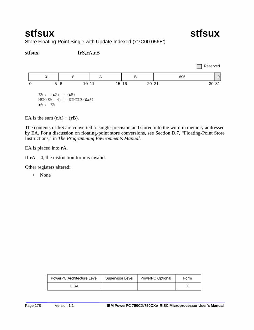
stfsux stfsux Store Floating-Point Single with Update Indexed (x’7C00 056E’)
stfsux frS,rA,rB
EA ← (rA) + (rB)MEM(EA, 4) ← SINGLE(frS)rA ← EA
EA is the sum (rA) + (rB).
The contents of frS are converted to single-precision and stored into the word in memory addressedby EA. For a discussion on floating-point store conversions, see Section D.7, “Floating-Point StoreInstructions,” in The Programming Environments Manual.
EA is placed into rA.
If rA = 0, the instruction form is invalid.
Other registers altered:
• None
Reserved
0 5 6 10 11 15 16 20 21 30 31
31 S A B 695 0
PowerPC Architecture Level Supervisor Level PowerPC Optional Form
UISA X
Page 178 Version 1.1 IBM PowerPC 750CX/750CXe RISC Microprocessor U
ser’s Manual
stfsx stfsx Store Floating-Point Single Indexed (x’7C00 052E’)
stfsx frS,rA,rB
if rA = 0 then b ← 0else b ← (rA)EA ← b + (rB)MEM(EA, 4) ← SINGLE(frS)
EA is the sum (rA|0) + (rB).
The contents of register frS are converted to single-precision and stored into the word in memoryaddressed by EA. For a discussion on floating-point store conversions, see Section D.7,“Floating-Point Store Instructions,” in The Programming Environments Manual.
Other registers altered:
• None
Reserved
0 5 6 10 11 15 16 20 21 30 31
31 S A B 663 0
PowerPC Architecture Level Supervisor Level PowerPC Optional Form
UISA X
Table of Contents 5/9/02
Page 179
sth sthStore Half Word (x’B000 0000’)
sth rS,d(rA)
if rA = 0 then b ← 0else b ← (rA)EA ← b + EXTS(d)MEM(EA, 2) ← rS[16-31]
EA is the sum (rA|0) + d. The contents of the low-order 16 bits of rS are stored into the half word inmemory addressed by EA.
Other registers altered:
• None
0 5 6 10 11 15 16 31
44 S A d
PowerPC Architecture Level Supervisor Level PowerPC Optional Form
UISA D
P
age 180 Version 1.1 IBM PowerPC 750CX/750CXe RISC Microprocessor User’s Manual
sthbrx sthbrxStore Half Word Byte-Reverse Indexed (x’7C00 072C’)
sthbrx rS,rA,rB
if rA = 0 then b ← 0else b ← (rA)EA ← b + (rB)MEM(EA, 2) ← rS[24-31] || rS[16-23]
EA is the sum (rA|0) + (rB). The contents of the low-order eight bits (24-31) of rS are stored into bits0–7 of the half word in memory addressed by EA. The contents of the subsequent low-order eight bits(16-23) of rS are stored into bits 8–15 of the half word in memory addressed by EA.
Other registers altered:
• None
Reserved
0 5 6 10 11 15 16 20 21 30 31
31 S A B 918 0
PowerPC Architecture Level Supervisor Level PowerPC Optional Form
UISA X
Table of Contents 5/9/02
Page 181
sthu sthuStore Half Word with Update (x’B400 0000’)
sthu rS,d(rA)
EA ← (rA) + EXTS(d)MEM(EA, 2) ← rS[16-31]rA ← EA
EA is the sum (rA) + d. The contents of the low-order 16 bits of rS are stored into the half word inmemory addressed by EA.
EA is placed into rA.
If rA = 0, the instruction form is invalid.
Other registers altered:
• None
0 5 6 10 11 15 16 31
45 S A d
PowerPC Architecture Level Supervisor Level PowerPC Optional Form
UISA D
P
age 182 Version 1.1 IBM PowerPC 750CX/750CXe RISC Microprocessor User’s Manual
sthux sthuxStore Half Word with Update Indexed (x’7C00 036E’)
sthux rS,rA,rB
EA ← (rA) + (rB)MEM(EA, 2) ← rS[16-31]rA ← EA
EA is the sum (rA) + (rB). The contents of the low-order 16 bits of rS are stored into the half wordin memory addressed by EA.
EA is placed into rA.
If rA = 0, the instruction form is invalid.
Other registers altered:
• None
Reserved
0 5 6 10 11 15 16 20 21 30 31
31 S A B 439 0
PowerPC Architecture Level Supervisor Level PowerPC Optional Form
UISA X
Table of Contents 5/9/02
Page 183
sthx sthxStore Half Word Indexed (x’7C00 032E’)
sthx rS,rA,rB
if rA = 0 then b ← 0else b ← (rA)EA ← b + (rB)MEM(EA, 2) ← rS[16-31]
EA is the sum (rA|0) + (rB). The contents of the low-order 16 bits of rS are stored into the half wordin memory addressed by EA.
Other registers altered:
• None
Reserved
0 5 6 10 11 15 16 20 21 30 31
31 S A B 407 0
PowerPC Architecture Level Supervisor Level PowerPC Optional Form
UISA X
Page 184 Version 1.1 IBM PowerPC 750CX/750CXe RISC Microprocessor U
ser’s Manual
stmw stmwStore Multiple Word (x’BC00 0000’)
stmw rS,d(rA)
if rA = 0 then b ← 0else b ← (rA)EA ← b + EXTS(d)r ← rS§do while r ð ≤ 31
MEM(EA, 4) ← GPR(r)r ← r + 1EA ← EA + 4
EA is the sum (rA|0) + d.
n = (32 – rS).
n consecutive words starting at EA are stored from the GPRs rS through r31. For example, if rS =30, 2 words are stored.
EA must be a multiple of four. If it is not, either the system alignment exception handler is invokedor the results are boundedly undefined. For additional information about alignment and DSIexceptions, see Section 6.4.3, “DSI Exception (0x00300),” in the PowerPC Microprocessor Family:The Programming Environments manual.
NOTE: In some implementations, this instruction is likely to have a greater latency and take longer to execute, perhaps much longer, than a sequence of individual store instructions that produce the same results.
Other registers altered:
• None
0 5 6 10 11 15 16 31
47 S A d
PowerPC Architecture Level Supervisor Level PowerPC Optional Form
UISA D
T
able of Contents 5/9/02 Page 185
stswi stswiStore String Word Immediate (x’7C00 05AA’)
stswi rS,rA,NB
if rA = 0 then EA ← 0else EA ← (rA)if NB = 0 then n ← 32else n ← NBr ← rS – 1i ← 0do while n > 0
if i = 0 then r ← r + 1 (mod 32)
MEM(EA, 1) ← GPR(r)[i,i + 7]i ← i + 8if i = 32
then i ← 0EA ← EA + 1n ← n – 1
EA is (rA|0). Let n = NB if NB ¦not_equal 0, n = 32 if NB = 0; n is the number of bytes to store. Letnr = CEIL(n /÷ 4); nr is the number of registers to supply data.
n consecutive bytes starting at EA are stored from GPRs rS through rS + nr – 1 Bytes are stored leftto right from each register. The sequence of registers wraps around through r0 if required.
Under certain conditions (for example, segment boundary crossing) the data alignment exceptionhandler may be invoked. For additional information about data alignment exceptions, seeSection 6.4.3, “DSI Exception (0x00300),” in the PowerPC Microprocessor Family: TheProgramming Environments manual.
NOTE: In some implementations, this instruction is likely to have a greater latency and take longer to execute, perhaps much longer, than a sequence of individual store instructions that produce the same results.
Other registers altered:
• None
Reserved
0 5 6 10 11 15 16 20 21 30 31
31 S A NB 725 0
PowerPC Architecture Level Supervisor Level PowerPC Optional Form
UISA X
Page 186 Version 1.1 IBM PowerPC 750CX/750CXe RISC Microprocessor U
ser’s Manual
stswx stswxStore String Word Indexed (x’7C00 052A’)
stswx rS,rA,rB
if rA = 0 then b ← 0else b ← (rA)EA ← b + (rB)n ← XER[25–31]r ← rS – 1i ← 0do while n > 0
if i = 0 then r ← r + 1 (mod 32)
MEM(EA, 1) ← GPR(r)[i,i + 7]i ← i + 8if i = 32
then i ← 0EA ← EA + 1n ← n – 1
EA is the sum (rA|0) + (rB). Let n = XER[25–31]; n is the number of bytes to store. Let nr = CEIL(n ÷/ 4); nr is the number of registers to supply data.
n consecutive bytes starting at EA are stored from GPRs rS through rS + nr – 1. Bytes are stored leftto right from each register. The sequence of registers wraps around through r0 if required. If n = 0,no bytes are stored.
Under certain conditions (for example, segment boundary crossing) the data alignment exceptionhandler may be invoked. For additional information about data alignment exceptions, seeSection 6.4.3, “DSI Exception (0x00300),” in the PowerPC Microprocessor Family: TheProgramming Environments manual.
NOTE: In some implementations, this instruction is likely to have a greater latency and take longer to execute, perhaps much longer, than a sequence of individual store instructions that produce the same results.
Other registers altered:
• None
Reserved
0 5 6 10 11 15 16 20 21 30 31
31 S A B 661 0
PowerPC Architecture Level Supervisor Level PowerPC Optional Form
UISA X
Table of Contents 5/9/02
Page 187
stw stwStore Word (x’9000 0000’)
stw rS,d(rA)
if rA = 0 then b ← 0else b ← (rA)EA ← b + EXTS(d)MEM(EA, 4) ← rS
EA is the sum (rA|0) + d. The contents of rS are stored into the word in memory addressed by EA.
Other registers altered:
• None
0 5 6 10 11 15 16 31
36 S A d
PowerPC Architecture Level Supervisor Level PowerPC Optional Form
UISA D
P
age 188 Version 1.1 IBM PowerPC 750CX/750CXe RISC Microprocessor User’s Manual
stwbrx stwbrxStore Word Byte-Reverse Indexed (x’7C00 052C’)
stwbrx rS,rA,rB
if rA = 0 then b ← 0else b ← (rA)EA ← b + (rB) MEM(EA, 4) ← rS[24-31] || rS[16-23] || rS[8-15] || rS[0-7]
EA is the sum (rA|0) + (rB). The contents of the low-order eight bits (24-31) of rS are stored into bits0–7 of the word in memory addressed by EA. The contents of the subsequent eight low-order bits(16-23) of rS are stored into bits 8–15 of the word in memory addressed by EA. The contents of thesubsequent eight low-order bits (8-15) of rS are stored into bits 16–23 of the word in memoryaddressed by EA. The contents of the subsequent eight low-order bits (0-7) of rS are stored into bits24–31 of the word in memory addressed by EA.
Other registers altered:
• None
Reserved
0 5 6 10 11 15 16 20 21 30 31
31 S A B 662 0
PowerPC Architecture Level Supervisor Level PowerPC Optional Form
UISA X
Table of Contents 5/9/02
Page 189
stwcx. stwcx.Store Word Conditional Indexed (x’7C00 012D’)stwcx. rS,rA,rB
if rA = 0 then b ← 0else b ← (rA)EA ← b + (rB)if RESERVE
thenMEM(EA, 4) ← rSCR0 ← 0b00 || 0b1 || XER[SO]RESERVE ← 0
elseCR0 ← 0b00 || 0b0 || XER[SO]
EA is the sum (rA|0) + (rB). If the reserved bit is set, the stwcx. instruction stores rS to effectiveaddress (rA + rB), clears the reserved bit, and sets CR0[EQ]. If the reserved bit is not set, the stwcx.instruction does not do a store; it leaves the reserved bit cleared and clears CR0[EQ]. Software mustlook at CR0[EQ] to see if the stwcx. was successful.
The reserved bit is set by the lwarx instruction. The reserved bit is cleared by any stwcx. instructionto any address, and also by snooping logic if it detects that another processor does any kind of writeor invalidate to the block indicated in the reservation buffer when reserved is set.
EA must be a multiple of four. If it is not, either the system alignment exception handler is invokedor the results are boundedly undefined. For additional information about alignment and DSIexceptions, see Section 6.4.3, “DSI Exception (0x00300),” in the PowerPC Microprocessor Family:The Programming Environments manual.
The granularity with which reservations are managed is implementation-dependent. Therefore, thememory to be accessed by the load and reserve and store conditional instructions should be controlledby a system library program.
Because the hardware doesn’t compare reservation address when executing the stwcx. instruction,operating systems software MUST reset the reservation if an exception or other type of interruptoccurs to insure atomic memory references of lwarx and stwcx. pairs.
Other registers altered:
• CR0 field is set to reflect whether the store operation was performed as follows: CR0[LT GT EQ S0] = 0b00 || store_performed || XER[SO]
• Condition Register (CR0 field)
Affected: LT, GT, EQ, SO
0 5 6 10 11 15 16 20 21 30 31
31 S A B 150 1
PowerPC Architecture Level Supervisor Level PowerPC Optional Form
UISA X
P
age 190 Version 1.1 IBM PowerPC 750CX/750CXe RISC Microprocessor User’s Manual
stwu stwuStore Word with Update (x’9400 0000’)
stwu rS,d(rA)
EA ← (rA) + EXTS(d)MEM(EA, 4) ← rSrA ← EA
EA is the sum (rA) + d. The contents of rS are stored into the word in memory addressed by EA.
EA is placed into rA.
If rA = 0, the instruction form is invalid.
Other registers altered:
• None
0 5 6 10 11 15 16 31
37 S A d
PowerPC Architecture Level Supervisor Level PowerPC Optional Form
UISA D
T
able of Contents 5/9/02 Page 191
stwux stwuxStore Word with Update Indexed (x’7C00 016E’)
stwux rS,rA,rB
EA ← (rA) + (rB)MEM(EA, 4) ← rSrA ← EA
EA is the sum (rA) + (rB). The contents of rS are stored into the word in memory addressed by EA.
EA is placed into rA.
If rA = 0, the instruction form is invalid.
Other registers altered:
• None
Reserved
0 5 6 10 11 15 16 20 21 30 31
31 S A B 183 0
PowerPC Architecture Level Supervisor Level PowerPC Optional Form
UISA X
Page 192 Version 1.1 IBM PowerPC 750CX/750CXe RISC Microprocessor U
ser’s Manual
stwx stwxStore Word Indexed (x’7C00 012E’)
stwx rS,rA,rB
if rA = 0 then b ← 0else b ← (rA)EA ← b + (rB)MEM(EA, 4) ← rS
EA is the sum (rA|0) + (rB). The contents of rS are stored into the word in memory addressed by EA.
Other registers altered:
• None
Reserved
0 5 6 10 11 15 16 20 21 30 31
31 S A B 151 0
PowerPC Architecture Level Supervisor Level PowerPC Optional Form
UISA X
Table of Contents 5/9/02
Page 193
subfx subfxSubtract From (x’7C00 0050’)
subf rD,rA,rB (OE = 0 Rc = 0)subf. rD,rA,rB (OE = 0 Rc = 1) subfo rD,rA,rB (OE = 1 Rc = 0) subfo. rD,rA,rB (OE = 1 Rc = 1)
rD ← ¬ (rA) + (rB) + 1
The sum ¬ (rA) + (rB) + 1 is placed into rD. (equivlent to (rB)--(rA))
The subf instruction is preferred for subtraction because it sets few status bits.
Other registers altered:
• Condition Register (CR0 field)
Affected: LT, GT, EQ, SO (if Rc = 1)
• XER
Affected: SO, OV (if OE = 1)
Simplified mnemonics:
sub rD,rA,rB equivalent to subf rD,rB,rA
0 5 6 10 11 15 16 20 21 22 30 31
31 D A B OE 40 Rc
PowerPC Architecture Level Supervisor Level PowerPC Optional Form
UISA XO
P
age 194 Version 1.1 IBM PowerPC 750CX/750CXe RISC Microprocessor User’s Manual
subfcx subfcx Subtract from Carrying (x’7C00 0010’)
subfc rD,rA,rB (OE = 0 Rc = 0)subfc. rD,rA,rB (OE = 0 Rc = 1)subfco rD,rA,rB (OE = 1 Rc = 0)subfco. rD,rA,rB (OE = 1 Rc = 1)
rD ← ¬ (rA) + (rB) + 1
The sum ¬ (rA) + (rB) + 1 is placed into rD. (equivlent to (rB)--(rA))
Other registers altered:
• Condition Register (CR0 field)
Affected: LT, GT, EQ, SO (if Rc = 1)
NOTE: CR0 field may not reflect the infinitely precise result if overflow occurs (see next).
• XER
Affected: CA
Affected: SO, OV (if OE = 1)
NOTE: The setting of the affected bits in the XER reflects overflow of the 32-bit results. For further information see Chapter 3, “Operand Conventions” in the PowerPC Microprocessor Family: The Programming Environments manual.
Simplified mnemonics:
subc rD,rA,rB equivalent to subfc rD,rB,rA
0 5 6 10 11 15 16 20 21 22 30 31
31 D A B OE 8 Rc
PowerPC Architecture Level Supervisor Level PowerPC Optional Form
UISA XO
T
able of Contents 5/9/02 Page 195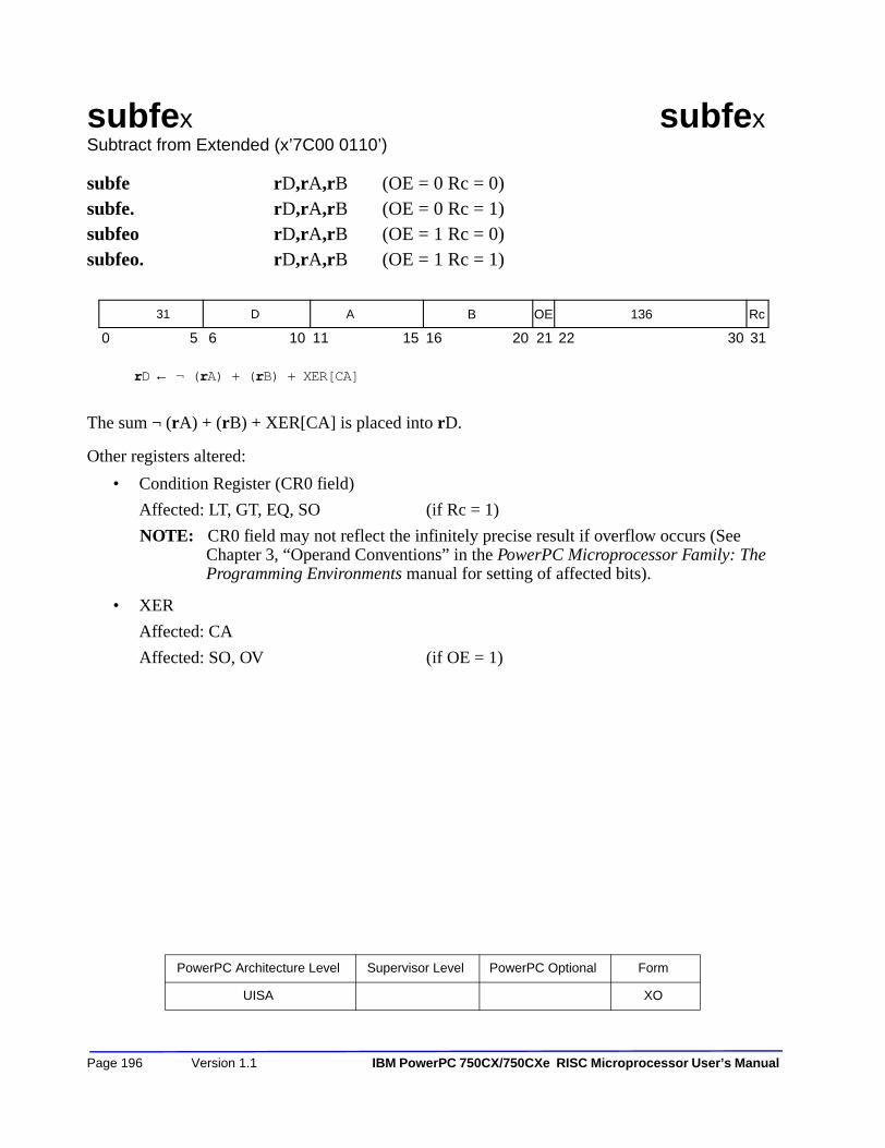
subfex subfex Subtract from Extended (x’7C00 0110’)
subfe rD,rA,rB (OE = 0 Rc = 0)subfe. rD,rA,rB (OE = 0 Rc = 1)subfeo rD,rA,rB (OE = 1 Rc = 0)subfeo. rD,rA,rB (OE = 1 Rc = 1)
rD ← ¬ (rA) + (rB) + XER[CA]
The sum ¬ (rA) + (rB) + XER[CA] is placed into rD.
Other registers altered:
• Condition Register (CR0 field)
Affected: LT, GT, EQ, SO (if Rc = 1)
NOTE: CR0 field may not reflect the infinitely precise result if overflow occurs (See Chapter 3, “Operand Conventions” in the PowerPC Microprocessor Family: The Programming Environments manual for setting of affected bits).
• XER
Affected: CA
Affected: SO, OV (if OE = 1)
0 5 6 10 11 15 16 20 21 22 30 31
31 D A B OE 136 Rc
PowerPC Architecture Level Supervisor Level PowerPC Optional Form
UISA XO
P
age 196 Version 1.1 IBM PowerPC 750CX/750CXe RISC Microprocessor User’s Manual
subfic subfic Subtract from Immediate Carrying (x’2000 0000’)
subfic rD,rA,SIMM
rD ← ¬ (rA) + EXTS(SIMM) + 1
The sum ¬ (rA) + EXTS(SIMM) + 1 is placed into rD (Equivalent to EXTS(SIMM)-(rA)).
Other registers altered:
• XER
Affected: CA
0 5 6 10 11 15 16 31
08 D A SIMM
PowerPC Architecture Level Supervisor Level PowerPC Optional Form
UISA D
T
able of Contents 5/9/02 Page 197
subfmex subfmex Subtract from Minus One Extended (x’7C00 01D0’)
subfme rD,rA (OE = 0 Rc = 0)subfme. rD,rA (OE = 0 Rc = 1)subfmeo rD,rA (OE = 1 Rc = 0)subfmeo. rD,rA (OE = 1 Rc = 1)
rD ← ¬ (rA) + XER[CA] – 1
The sum ¬ (rA) + XER[CA] + (32)1 is placed into rD.
Other registers altered:
• Condition Register (CR0 field)
Affected: LT, GT, EQ, SO (if Rc = 1)
NOTE: CR0 field may not reflect the infinitely precise result if overflow occurs (See Chapter 3, “Operand Conventions,” in the PowerPC Microprocessor Family: The Programming Environments manual.)
• XER
Affected: CA
Affected: SO, OV (if OE = 1)
0 5 6 10 11 15 16 20 21 22 30 31
31 D A
Reserved
0 0 0 0 0 OE 232 Rc
PowerPC Architecture Level Supervisor Level PowerPC Optional Form
UISA XO
P
age 198 Version 1.1 IBM PowerPC 750CX/750CXe RISC Microprocessor U ser’s Manual
subfzex subfzex Subtract from Zero Extended (x’7C00 0190’)
subfze rD,rA (OE = 0 Rc = 0)subfze. rD,rA (OE = 0 Rc = 1)subfzeo rD,rA (OE = 1 Rc = 0)subfzeo. rD,rA (OE = 1 Rc = 1)
rD ← ¬ (rA) + XER[CA]
The sum ¬ (rA) + XER[CA] is placed into rD.
Other registers altered:
• Condition Register (CR0 field)
Affected: LT, GT, EQ, SO (if Rc = 1)
NOTE: CR0 field may not reflect the infinitely precise result if overflow occurs (see next).
• XER
Affected: CA
Affected: SO, OV (if OE = 1)
NOTE: See Chapter 3, “Operand Conventions,” in the PowerPC Microprocessor Family: The Programming Environments manual.
0 5 6 10 11 15 16 20 21 22 30 31
31 D A
Reserved
0 0 0 0 0 OE 200 Rc
PowerPC Architecture Level Supervisor Level PowerPC Optional Form
UISA XO
T
able of Contents 5/9/02 Page 199
sync syncSynchronize (x’7C00 04AC’)
The sync instruction provides an ordering function for the effects of all instructions executed by agiven processor. Executing a sync instruction ensures that all instructions preceding the syncinstruction appear to have completed before the sync instruction completes, and that no subsequentinstructions are initiated by the processor until after the sync instruction completes. When the syncinstruction completes, all external accesses caused by instructions preceding the sync instruction willhave been performed with respect to all other mechanisms that access memory. For more informationon how the sync instruction affects the VEA, refer to Chapter 5, “Cache Model and MemoryCoherency” in the PowerPC Microprocessor Family: The Programming Environments manual.Multiprocessor implementations also send a sync address-only broadcast that is useful in somedesigns. For example, if a design has an external buffer that re-orders loads and stores for better busefficiency, the sync broadcast signals to that buffer that previous loads/stores must be completedbefore any following loads/stores.
The sync instruction can be used to ensure that the results of all stores into a data structure, causedby store instructions executed in a “critical section” of a program, are seen by other processors beforethe data structure is seen as unlocked.
The functions performed by the sync instruction will normally take a significant amount of time tocomplete, so indiscriminate use of this instruction may adversely affect performance. In addition, thetime required to execute sync may vary from one execution to another.
The eieio instruction may be more appropriate than sync for many cases.
This instruction is execution synchronizing. For more information on execution synchronization, seeSection 4.1.5, “Synchronizing Instructions,” in The Programming Environments Manual.
Other registers altered:
• None
0 0 0 0 0 598 0
0 5 6 10 11 15 16 20 21 30 31
Reserved
31 0 0 0 0 0 0 0 0 00
PowerPC Architecture Level Supervisor Level PowerPC Optional Form
UISA X
Page 200 Version 1.1 IBM Pow
erPC 750CX/750CXe RISC Microprocessor U ser’s Manual
tlbie tlbie Translation Lookaside Buffer Invalidate Entry (x’7C00 0264’)
tlbie rB
VPS ← rB[4-19] Identify TLB entries corresponding to VPSEach such TLB entry ← invalid
EA is the contents of rB. If the translation lookaside buffer (TLB) contains an entry corresponding toEA, that entry is made invalid (that is, removed from the TLB).
Multiprocessing implementations (for example, the 601, and 604) send a tlbie address-only broadcastover the address bus to tell other processors to invalidate the same TLB entry in their TLBs.
The TLB search is done regardless of the settings of MSR[IR] and MSR[DR]. The search is donebased on a portion of the logical page number within a segment, without reference to the SLB,segment table, or segment registers. All entries matching the search criteria are invalidated.
Block address translation for EA, if any, is ignored. Refer to Section 7.5.3.4, “Synchronization ofMemory Accesses and Referenced and Changed Bit Updates” and Section 7.6.3, “Page TableUpdates” in the PowerPC Microprocessor Family: The Programming Environments manual for otherrequirements associated with the use of this instruction.
This is a supervisor-level instruction and optional in the PowerPC architecture.
Other registers altered:
• None
0 5 6 10 11 15 16 20 21 30 31
Reserved
31 0 0 0 0 0 0 0 0 0 0 B 306 0
PowerPC Architecture Level Supervisor Level PowerPC Optional Form
OEA YES YES X
T
able of Contents 5/9/02 Page 201
tlbsync tlbsyncTLB Synchronize (x’7C00 046C’)
If an implementation sends a broadcast for tlbie then it will also send a broadcast for tlbsync.Executing a tlbsync instruction ensures that all tlbie instructions previously executed by theprocessor executing the tlbsync instruction have completed on all other processors.
The operation performed by this instruction is treated as a caching-inhibited and guarded data accesswith respect to the ordering done by eieio.
The 601 expands the use of the sync instruction to cover tlbsync functionality.
Refer to Section 7.5.3.4, “Synchronization of Memory Accesses and Referenced and Changed BitUpdates” and Section 7.6.3, “Page Table Updates” in the PowerPC Microprocessor Family: TheProgramming Environments manual for other requirements associated with the use of this instruction.
This instruction is supervisor-level and optional in the PowerPC architecture.
Other registers altered:
• None
0 5 6 10 11 15 16 20 21 30 31
Reserved
31 0 0 0 0 0 0 0 0 0 0 0 0 0 0 0 566 0
PowerPC Architecture Level Supervisor Level PowerPC Optional Form
OEA YES YES X
P
age 202 Version 1.1 IBM PowerPC 750CX/750CXe RISC Microprocessor U ser’s Manual
tw tw Trap Word (x’7C00 0008’)
tw TO,rA,rB
a ← EXTS(rA)b ← EXTS(rB)if (a < b) & TO[0] then TRAPif (a > b) & TO[1] then TRAPif (a = b) & TO[2] then TRAPif (a <U b) & TO[3] then TRAPif (a >U b) & TO[4] then TRAP
The contents of rA are compared arithmetically with the contents rB for TO[0, 1, 2]. The contents ofrA are compared logically with the contents rB for TO[3, 4]. If any bit in the TO field is set and itscorresponding condition is met by the result of the comparison, then the system trap handler isinvoked.
Other registers altered:
• None
Simplified mnemonics:
tweq rA,rB equivalent to tw 4,rA,rBtwlgerA,rB equivalent to tw 5,rA,rBtrap equivalent to tw 31,0,0
0 5 6 10 11 15 16 20 21 30 31
Reserved
31 TO A B 4 0
PowerPC Architecture Level Supervisor Level PowerPC Optional Form
UISA X
T
able of Contents 5/9/02 Page 203
twi twi Trap Word Immediate (x’0C00 0000’)
twi TO,rA,SIMM
a ← EXTS(rA)if (a < EXTS(SIMM)) & TO[0] then TRAPif (a > EXTS(SIMM)) & TO[1] then TRAPif (a = EXTS(SIMM)) & TO[2] then TRAPif (a <U EXTS(SIMM)) & TO[3] then TRAPif (a >U EXTS(SIMM)) & TO[4] then TRAP
The contents of rA are compared arithmetically with the sign-extended value of the SIMM field forTO[0, 1, 2]. The contents of rA are compared logically with the sign-extended value of the SIMMfield for TO[3, 4]. If any bit in the TO field is set and its corresponding condition is met by the resultof the comparison, then the system trap handler is invoked.
Other registers altered:
• None
Simplified mnemonics:
twgtirA,value equivalent to twi 8,rA,valuetwlleirA,value equivalent to twi 6,rA,value
0 5 6 10 11 15 16 31
03 TO A SIMM
PowerPC Architecture Level Supervisor Level PowerPC Optional Form
UISA D
P
age 204 Version 1.1 IBM PowerPC 750CX/750CXe RISC Microprocessor User’s Manual
xorx xorxXOR (x’7C00 0278’)
xor rA,rS,rB (Rc = 0)xor. rA,rS,rB (Rc = 1)
rA ← (rS) ⊕ (rB)
The contents of rS are XORed with the contents of rB and the result is placed into rA.
Other registers altered:
• Condition Register (CR0 field)
Affected: LT, GT, EQ, SO (if Rc = 1)
0 5 6 10 11 15 16 20 21 30 31
31 S A B 316 Rc
PowerPC Architecture Level Supervisor Level PowerPC Optional Form
UISA X
T
able of Contents 5/9/02 Page 205
xori xori XOR Immediate (x’6800 0000’)
xori rA,rS,UIMM
rA ← (rS) ⊕ ((16)0 || UIMM)
The contents of rS are XORed with 0x0000 || UIMM and the result is placed into rA.
Other registers altered:
• None
0 5 6 10 11 15 16 31
26 S A UIMM
PowerPC Architecture Level Supervisor Level PowerPC Optional Form
UISA D
P
age 206 Version 1.1 IBM PowerPC 750CX/750CXe RISC Microprocessor User’s Manual
xoris xoris XOR Immediate Shifted (x’6C00 0000’)
xoris rA,rS,UIMM
rA ← (rS) ⊕ (UIMM || (16)0)
The contents of rS are XORed with UIMM || 0x0000 and the result is placed into rA.
Other registers altered:
• None
0 5 6 10 11 15 16 31
27 S A UIMM
PowerPC Architecture Level Supervisor Level PowerPC Optional Form
UISA D
T
able of Contents 5/9/02 Page 207
Page 208 Version 1.1 IBM PowerPC 750CX/750CXe RISC Microprocessor User’s Manual

Appendix A 750CX Instruction Set
A.1 Instructions Sorted by OpcodeTable A-1 lists the instructions defined in the PowerPC architecture in numeric order by opcode.
Table A-1 Complete Instruction List Sorted by Opcode
Name 0 5 6 7 8 9 10 11 12 13 14 15 16 17 18 19 20 21 22 23 24 25 26 27 28 29 30 31
twi 0 0 0 0 1 1 TO A SIMM
mulli 0 0 0 1 1 1 D A SIMM
subfic 0 0 1 0 0 0 D A SIMM
cmpli 0 0 1 0 1 0 crfD 0 L A UIMM
cmpi 0 0 1 0 1 1 crfD 0 L A SIMM
addic 0 0 1 1 0 0 D A SIMM
addic. 0 0 1 1 0 1 D A SIMM
addi 0 0 1 1 1 0 D A SIMM
addis 0 0 1 1 1 1 D A SIMM
bcx 0 1 0 0 0 0 BO BI BD AA LK
sc 0 1 0 0 0 1 0 0 0 0 0 0 0 0 0 0 0 0 0 0 0 0 0 0 0 0 0 0 0 0 0 1 0
bx 0 1 0 0 1 0 LI AA LK
mcrf 0 1 0 0 1 1 crfD 0 0 crfS 0 0 0 0 0 0 0 0 0 0 0 0 0 0 0 0 0 0
bclrx 0 1 0 0 1 1 BO BI 0 0 0 0 0 0 0 0 0 0 1 0 0 0 0 LK
crnor 0 1 0 0 1 1 crbD crbA crbB 0 0 0 0 1 0 0 0 0 1 0
rfi 0 1 0 0 1 1 0 0 0 0 0 0 0 0 0 0 0 0 0 0 0 0 0 0 0 1 1 0 0 1 0 0
crandc 0 1 0 0 1 1 crbD crbA crbB 0 0 1 0 0 0 0 0 0 1 0
isync 0 1 0 0 1 1 0 0 0 0 0 0 0 0 0 0 0 0 0 0 0 0 0 1 0 0 1 0 1 1 0 0
crxor 0 1 0 0 1 1 crbD crbA crbB 0 0 1 1 0 0 0 0 0 1 0
crnand 0 1 0 0 1 1 crbD crbA crbB 0 0 1 1 1 0 0 0 0 1 0
crand 0 1 0 0 1 1 crbD crbA crbB 0 1 0 0 0 0 0 0 0 1 0
creqv 0 1 0 0 1 1 crbD crbA crbB 0 1 0 0 1 0 0 0 0 1 0
crorc 0 1 0 0 1 1 crbD crbA crbB 0 1 1 0 1 0 0 0 0 1 0
cror 0 1 0 0 1 1 crbD crbA crbB 0 1 1 1 0 0 0 0 0 1 0
Reserved bits
Key:
Table of Contents 5/9/02 Page 1

bcctrx 0 1 0 0 1 1 BO BI 0 0 0 0 0 1 0 0 0 0 1 0 0 0 0 LK
rlwimix 0 1 0 1 0 0 S A SH MB ME Rc
rlwinmx 0 1 0 1 0 1 S A SH MB ME Rc
rlwnmx 0 1 0 1 1 1 S A B MB ME Rc
ori 0 1 1 0 0 0 S A UIMM
oris 0 1 1 0 0 1 S A UIMM
xori 0 1 1 0 1 0 S A UIMM
xoris 0 1 1 0 1 1 S A UIMM
andi. 0 1 1 1 0 0 S A UIMM
andis. 0 1 1 1 0 1 S A UIMM
cmp 0 1 1 1 1 1 crfD 0 L A B 0 0 0 0 0 0 0 0 0 0 0
tw 0 1 1 1 1 1 TO A B 0 0 0 0 0 0 0 1 0 0 0
subfcx 0 1 1 1 1 1 D A B OE 0 0 0 0 0 0 1 0 0 0 Rc
addcx 0 1 1 1 1 1 D A B OE 0 0 0 0 0 0 1 0 1 0 Rc
mulhwux 0 1 1 1 1 1 D A B 0 0 0 0 0 0 0 1 0 1 1 Rc
mfcr 0 1 1 1 1 1 D 0 0 0 0 0 0 0 0 0 0 0 0 0 0 0 1 0 0 1 1 0
lwarx 0 1 1 1 1 1 D A B 0 0 0 0 0 1 0 1 0 0 0
lwzx 0 1 1 1 1 1 D A B 0 0 0 0 0 1 0 1 1 1 0
slwx 0 1 1 1 1 1 S A B 0 0 0 0 0 1 1 0 0 0 Rc
cntlzwx 0 1 1 1 1 1 S A 0 0 0 0 0 0 0 0 0 0 1 1 0 1 0 Rc
andx 0 1 1 1 1 1 S A B 0 0 0 0 0 1 1 1 0 0 Rc
cmpl 0 1 1 1 1 1 crfD 0 L A B 0 0 0 0 1 0 0 0 0 0 0
subfx 0 1 1 1 1 1 D A B OE 0 0 0 0 1 0 1 0 0 0 Rc
dcbst 0 1 1 1 1 1 0 0 0 0 0 A B 0 0 0 0 1 1 0 1 1 0 0
lwzux 0 1 1 1 1 1 D A B 0 0 0 0 1 1 0 1 1 1 0
andcx 0 1 1 1 1 1 S A B 0 0 0 0 1 1 1 1 0 0 Rc
mulhwx 0 1 1 1 1 1 D A B 0 0 0 0 1 0 0 1 0 1 1 Rc
mfmsr 0 1 1 1 1 1 D 0 0 0 0 0 0 0 0 0 0 0 0 0 1 0 1 0 0 1 1 0
dcbf 0 1 1 1 1 1 0 0 0 0 0 A B 0 0 0 1 0 1 0 1 1 0 0
lbzx 0 1 1 1 1 1 D A B 0 0 0 1 0 1 0 1 1 1 0
negx 0 1 1 1 1 1 D A 0 0 0 0 0 OE 0 0 0 1 1 0 1 0 0 0 Rc
lbzux 0 1 1 1 1 1 D A B 0 0 0 1 1 1 0 1 1 1 0
Name 0 5 6 7 8 9 10 11 12 13 14 15 16 17 18 19 20 21 22 23 24 25 26 27 28 29 30 31
Page 2 Version 1.1 IBM PowerPC 750CX/750CXe RISC Microprocessor User’s Manual

norx 0 1 1 1 1 1 S A B 0 0 0 1 1 1 1 1 0 0 Rc
subfex 0 1 1 1 1 1 D A B OE 0 0 1 0 0 0 1 0 0 0 Rc
addex 0 1 1 1 1 1 D A B OE 0 0 1 0 0 0 1 0 1 0 Rc
mtcrf 0 1 1 1 1 1 S 0 CRM 0 0 0 1 0 0 1 0 0 0 0 0
mtmsr 0 1 1 1 1 1 S 0 0 0 0 0 0 0 0 0 0 0 0 1 0 0 1 0 0 1 0 0
stwcx. 0 1 1 1 1 1 S A B 0 0 1 0 0 1 0 1 1 0 1
stwx 0 1 1 1 1 1 S A B 0 0 1 0 0 1 0 1 1 1 0
stwux 0 1 1 1 1 1 S A B 0 0 1 0 1 1 0 1 1 1 0
subfzex 0 1 1 1 1 1 D A 0 0 0 0 0 OE 0 0 1 1 0 0 1 0 0 0 Rc
addzex 0 1 1 1 1 1 D A 0 0 0 0 0 OE 0 0 1 1 0 0 1 0 1 0 Rc
mtsr 0 1 1 1 1 1 S 0 SR 0 0 0 0 0 0 0 1 1 0 1 0 0 1 0 0
stbx 0 1 1 1 1 1 S A B 0 0 1 1 0 1 0 1 1 1 0
subfmex 0 1 1 1 1 1 D A 0 0 0 0 0 OE 0 0 1 1 1 0 1 0 0 0 Rc
addmex 0 1 1 1 1 1 D A 0 0 0 0 0 OE 0 0 1 1 1 0 1 0 1 0 Rc
mullwx 0 1 1 1 1 1 D A B OE 0 0 1 1 1 0 1 0 1 1 Rc
mtsrin 0 1 1 1 1 1 S 0 0 0 0 0 B 0 0 1 1 1 1 0 0 1 0 0
dcbtst 0 1 1 1 1 1 0 0 0 0 0 A B 0 0 1 1 1 1 0 1 1 0 0
stbux 0 1 1 1 1 1 S A B 0 0 1 1 1 1 0 1 1 1 0
addx 0 1 1 1 1 1 D A B OE 0 1 0 0 0 0 1 0 1 0 Rc
dcbt 0 1 1 1 1 1 0 0 0 0 0 A B 0 1 0 0 0 1 0 1 1 0 0
lhzx 0 1 1 1 1 1 D A B 0 1 0 0 0 1 0 1 1 1 0
eqvx 0 1 1 1 1 1 S A B 0 1 0 0 0 1 1 1 0 0 Rc
tlbie 0 1 1 1 1 1 0 0 0 0 0 0 0 0 0 0 B 0 1 0 0 1 1 0 0 1 0 0
eciwx 0 1 1 1 1 1 D A B 0 1 0 0 1 1 0 1 1 0 0
lhzux 0 1 1 1 1 1 D A B 0 1 0 0 1 1 0 1 1 1 0
xorx 0 1 1 1 1 1 S A B 0 1 0 0 1 1 1 1 0 0 Rc
mfspr 0 1 1 1 1 1 D spr 0 1 0 1 0 1 0 0 1 1 0
lhax 0 1 1 1 1 1 D A B 0 1 0 1 0 1 0 1 1 1 0
mftb 0 1 1 1 1 1 D tbr 0 1 0 1 1 1 0 0 1 1 0
lhaux 0 1 1 1 1 1 D A B 0 1 0 1 1 1 0 1 1 1 0
sthx 0 1 1 1 1 1 S A B 0 1 1 0 0 1 0 1 1 1 0
orcx 0 1 1 1 1 1 S A B 0 1 1 0 0 1 1 1 0 0 Rc
Name 0 5 6 7 8 9 10 11 12 13 14 15 16 17 18 19 20 21 22 23 24 25 26 27 28 29 30 31
Table of Contents 5/9/02 Page 3

ecowx 0 1 1 1 1 1 S A B 0 1 1 0 1 1 0 1 1 0 0
sthux 0 1 1 1 1 1 S A B 0 1 1 0 1 1 0 1 1 1 0
orx 0 1 1 1 1 1 S A B 0 1 1 0 1 1 1 1 0 0 Rc
divwux 0 1 1 1 1 1 D A B OE 0 1 1 1 0 0 1 0 1 1 Rc
mtspr 0 1 1 1 1 1 S spr 0 1 1 1 0 1 0 0 1 1 0
dcbi 0 1 1 1 1 1 0 0 0 0 0 A B 0 1 1 1 0 1 0 1 1 0 0
nandx 0 1 1 1 1 1 S A B 0 1 1 1 0 1 1 1 0 0 Rc
divwx 0 1 1 1 1 1 D A B OE 0 1 1 1 1 0 1 0 1 1 Rc
mcrxr 0 1 1 1 1 1 crfD 0 0 0 0 0 0 0 0 0 0 0 0 1 0 0 0 0 0 0 0 0 0 0
lswx 0 1 1 1 1 1 D A B 1 0 0 0 0 1 0 1 0 1 0
lwbrx 0 1 1 1 1 1 D A B 1 0 0 0 0 1 0 1 1 0 0
lfsx 0 1 1 1 1 1 D A B 1 0 0 0 0 1 0 1 1 1 0
srwx 0 1 1 1 1 1 S A B 1 0 0 0 0 1 1 0 0 0 Rc
tlbsync 0 1 1 1 1 1 0 0 0 0 0 0 0 0 0 0 0 0 0 0 0 1 0 0 0 1 1 0 1 1 0 0
lfsux 0 1 1 1 1 1 D A B 1 0 0 0 1 1 0 1 1 1 0
mfsr 0 1 1 1 1 1 D 0 SR 0 0 0 0 0 1 0 0 1 0 1 0 0 1 1 0
lswi 0 1 1 1 1 1 D A NB 1 0 0 1 0 1 0 1 0 1 0
sync 0 1 1 1 1 1 0 0 0 0 0 0 0 0 0 0 0 0 0 0 0 1 0 0 1 0 1 0 1 1 0 0
lfdx 0 1 1 1 1 1 D A B 1 0 0 1 0 1 0 1 1 1 0
lfdux 0 1 1 1 1 1 D A B 1 0 0 1 1 1 0 1 1 1 0
mfsrin 0 1 1 1 1 1 D 0 0 0 0 0 B 1 0 1 0 0 1 0 0 1 1 0
stswx 0 1 1 1 1 1 S A B 1 0 1 0 0 1 0 1 0 1 0
stwbrx 0 1 1 1 1 1 S A B 1 0 1 0 0 1 0 1 1 0 0
stfsx 0 1 1 1 1 1 S A B 1 0 1 0 0 1 0 1 1 1 0
stfsux 0 1 1 1 1 1 S A B 1 0 1 0 1 1 0 1 1 1 0
stswi 0 1 1 1 1 1 S A NB 1 0 1 1 0 1 0 1 0 1 0
stfdx 0 1 1 1 1 1 S A B 1 0 1 1 0 1 0 1 1 1 0
stfdux 0 1 1 1 1 1 S A B 1 0 1 1 1 1 0 1 1 1 0
lhbrx 0 1 1 1 1 1 D A B 1 1 0 0 0 1 0 1 1 0 0
srawx 0 1 1 1 1 1 S A B 1 1 0 0 0 1 1 0 0 0 Rc
srawix 0 1 1 1 1 1 S A SH 1 1 0 0 1 1 1 0 0 0 Rc
eieio 0 1 1 1 1 1 0 0 0 0 0 0 0 0 0 0 0 0 0 0 0 1 1 0 1 0 1 0 1 1 0 0
Name 0 5 6 7 8 9 10 11 12 13 14 15 16 17 18 19 20 21 22 23 24 25 26 27 28 29 30 31
Page 4 Version 1.1 IBM PowerPC 750CX/750CXe RISC Microprocessor User’s Manual

sthbrx 0 1 1 1 1 1 S A B 1 1 1 0 0 1 0 1 1 0 0
extshx 0 1 1 1 1 1 S A 0 0 0 0 0 1 1 1 0 0 1 1 0 1 0 Rc
extsbx 0 1 1 1 1 1 S A 0 0 0 0 0 1 1 1 0 1 1 1 0 1 0 Rc
icbi 0 1 1 1 1 1 0 0 0 0 0 A B 1 1 1 1 0 1 0 1 1 0 0
stfiwx 0 1 1 1 1 1 S A B 1 1 1 1 0 1 0 1 1 1 0
dcbz 0 1 1 1 1 1 0 0 0 0 0 A B 1 1 1 1 1 1 0 1 1 0 0
lwz 1 0 0 0 0 0 D A d
lwzu 1 0 0 0 0 1 D A d
lbz 1 0 0 0 1 0 D A d
lbzu 1 0 0 0 1 1 D A d
stw 1 0 0 1 0 0 S A d
stwu 1 0 0 1 0 1 S A d
stb 1 0 0 1 1 0 S A d
stbu 1 0 0 1 1 1 S A d
lhz 1 0 1 0 0 0 D A d
lhzu 1 0 1 0 0 1 D A d
lha 1 0 1 0 1 0 D A d
lhau 1 0 1 0 1 1 D A d
sth 1 0 1 1 0 0 S A d
sthu 1 0 1 1 0 1 S A d
lmw 1 0 1 1 1 0 D A d
stmw 1 0 1 1 1 1 S A d
lfs 1 1 0 0 0 0 D A d
lfsu 1 1 0 0 0 1 D A d
lfd 1 1 0 0 1 0 D A d
lfdu 1 1 0 0 1 1 D A d
stfs 1 1 0 1 0 0 S A d
stfsu 1 1 0 1 0 1 S A d
stfd 1 1 0 1 1 0 S A d
stfdu 1 1 0 1 1 1 S A d
fdivsx 1 1 1 0 1 1 D A B 0 0 0 0 0 1 0 0 1 0 Rc
fsubsx 1 1 1 0 1 1 D A B 0 0 0 0 0 1 0 1 0 0 Rc
Name 0 5 6 7 8 9 10 11 12 13 14 15 16 17 18 19 20 21 22 23 24 25 26 27 28 29 30 31
Table of Contents 5/9/02 Page 5

faddsx 1 1 1 0 1 1 D A B 0 0 0 0 0 1 0 1 0 1 Rc
fresx 1 1 1 0 1 1 D 0 0 0 0 0 B 0 0 0 0 0 1 1 0 0 0 Rc
fmulsx 1 1 1 0 1 1 D A 0 0 0 0 0 C 1 1 0 0 1 Rc
fmsubsx 1 1 1 0 1 1 D A B C 1 1 1 0 0 Rc
fmaddsx 1 1 1 0 1 1 D A B C 1 1 1 0 1 Rc
fnmsubsx 1 1 1 0 1 1 D A B C 1 1 1 1 0 Rc
fnmaddsx 1 1 1 0 1 1 D A B C 1 1 1 1 1 Rc
fcmpu 1 1 1 1 1 1 crfD 0 0 A B 0 0 0 0 0 0 0 0 0 0 0
frspx 1 1 1 1 1 1 D 0 0 0 0 0 B 0 0 0 0 0 0 1 1 0 0 Rc
fctiwx 1 1 1 1 1 1 D 0 0 0 0 0 B 0 0 0 0 0 0 1 1 1 0
fctiwzx 1 1 1 1 1 1 D 0 0 0 0 0 B 0 0 0 0 0 0 1 1 1 1 Rc
fdivx 1 1 1 1 1 1 D A B 0 0 0 0 0 1 0 0 1 0 Rc
fsubx 1 1 1 1 1 1 D A B 0 0 0 0 0 1 0 1 0 0 Rc
faddx 1 1 1 1 1 1 D A B 0 0 0 0 0 1 0 1 0 1 Rc
fselx 1 1 1 1 1 1 D A B C 1 0 1 1 1 Rc
fmulx 1 1 1 1 1 1 D A 0 0 0 0 0 C 1 1 0 0 1 Rc
frsqrtex 1 1 1 1 1 1 D 0 0 0 0 0 B 0 0 0 0 0 1 1 0 1 0 Rc
fmsubx 1 1 1 1 1 1 D A B C 1 1 1 0 0 Rc
fmaddx 1 1 1 1 1 1 D A B C 1 1 1 0 1 Rc
fnmsubx 1 1 1 1 1 1 D A B C 1 1 1 1 0 Rc
fnmaddx 1 1 1 1 1 1 D A B C 1 1 1 1 1 Rc
fcmpo 1 1 1 1 1 1 crfD 0 0 A B 0 0 0 0 1 0 0 0 0 0 0
mtfsb1x 1 1 1 1 1 1 crbD 0 0 0 0 0 0 0 0 0 0 0 0 0 0 1 0 0 1 1 0 Rc
fnegx 1 1 1 1 1 1 D 0 0 0 0 0 B 0 0 0 0 1 0 1 0 0 0 Rc
mcrfs 1 1 1 1 1 1 crfD 0 0 crfS 0 0 0 0 0 0 0 0 0 0 1 0 0 0 0 0 0 0
mtfsb0x 1 1 1 1 1 1 crbD 0 0 0 0 0 0 0 0 0 0 0 0 0 1 0 0 0 1 1 0 Rc
fmrx 1 1 1 1 1 1 D 0 0 0 0 0 B 0 0 0 1 0 0 1 0 0 0 Rc
mtfsfix 1 1 1 1 1 1 crfD 0 0 0 0 0 0 0 IMM 0 0 0 1 0 0 0 0 1 1 0 Rc
fnabsx 1 1 1 1 1 1 D 0 0 0 0 0 B 0 0 1 0 0 0 1 0 0 0 Rc
fabsx 1 1 1 1 1 1 D 0 0 0 0 0 B 0 1 0 0 0 0 1 0 0 0 Rc
mffsx 1 1 1 1 1 1 D 0 0 0 0 0 0 0 0 0 0 1 0 0 1 0 0 0 1 1 1 Rc
mtfsfx 1 1 1 1 1 1 0 FM 0 B 1 0 1 1 0 0 0 1 1 1 Rc
Name 0 5 6 7 8 9 10 11 12 13 14 15 16 17 18 19 20 21 22 23 24 25 26 27 28 29 30 31
Page 6 Version 1.1 IBM PowerPC 750CX/750CXe RISC Microprocessor User’s Manual

A.2 Instructions Grouped by Functional CategoriesTable A-2 through Table A-29 list the 750CX instructions grouped by function.
Table A-2 Integer Arithmetic Instructions
Name 0 5 6 7 8 9 10 11 12 13 14 15 16 17 18 19 20 21 22 23 24 25 26 27 28 29 30 31
addx 31 D A B OE 266 Rc
addcx 31 D A B OE 10 Rc
addex 31 D A B OE 138 Rc
addi 14 D A SIMM
addic 12 D A SIMM
addic. 13 D A SIMM
addis 15 D A SIMM
addmex 31 D A 0 0 0 0 0 OE 234 Rc
addzex 31 D A 0 0 0 0 0 OE 202 Rc
divwx 31 D A B OE 491 Rc
divwux 31 D A B OE 459 Rc
mulhwx 31 D A B 0 75 Rc
mulhwux 31 D A B 0 11 Rc
mulli 07 D A SIMM
mullwx 31 D A B OE 235 Rc
negx 31 D A 0 0 0 0 0 OE 104 Rc
subfx 31 D A B OE 40 Rc
subfcx 31 D A B OE 8 Rc
subfex 31 D A B OE 136 Rc
subficx 08 D A SIMM
subfmex 31 D A 0 0 0 0 0 OE 232 Rc
subfzex 31 D A 0 0 0 0 0 OE 200 Rc
Reserved bitsKey:
Table of Contents 5/9/02 Page 7

Table A-3 Integer Compare Instructions
Table A-4 Integer Logical Instructions
Table A-5 Integer Rotate Instructions
Name 0 5 6 7 8 9 10 11 12 13 14 15 16 17 18 19 20 21 22 23 24 25 26 27 28 29 30 31
cmp 31 crfD 0 L A B 0 0
cmpi 11 crfD 0 L A SIMM
cmpl 31 crfD 0 L A B 32 0
cmpli 10 crfD 0 L A UIMM
Name 0 5 6 7 8 9 10 11 12 13 14 15 16 17 18 19 20 21 22 23 24 25 26 27 28 29 30 31
andx 31 S A B 28 Rc
andcx 31 S A B 60 Rc
andi. 28 S A UIMM
andis. 29 S A UIMM
cntlzwx 31 S A 0 0 0 0 0 26 Rc
eqvx 31 S A B 284 Rc
extsbx 31 S A 0 0 0 0 0 954 Rc
extshx 31 S A 0 0 0 0 0 922 Rc
nandx 31 S A B 476 Rc
norx 31 S A B 124 Rc
orx 31 S A B 444 Rc
orcx 31 S A B 412 Rc
ori 24 S A UIMM
oris 25 S A UIMM
xorx 31 S A B 316 Rc
xori 26 S A UIMM
xoris 27 S A UIMM
Name 0 5 6 7 8 9 10 11 12 13 14 15 16 17 18 19 20 21 22 23 24 25 26 27 28 29 30 31
rlwimix 20 S A SH MB ME Rc
rlwinmx 21 S A SH MB ME Rc
rlwnmx 23 S A SH MB ME Rc
Page 8 Version 1.1 IBM PowerPC 750CX/750CXe RISC Microprocessor User’s Manual

Table A-6 Integer Shift Instructions
Table A-7 Floating-Point Arithmetic Instructions
Table A-8 Floating-Point Multiply-Add Instructions
Name 0 5 6 7 8 9 10 11 12 13 14 15 16 17 18 19 20 21 22 23 24 25 26 27 28 29 30 31
slwx 31 S A B 24 Rc
srawx 31 S A B 792 Rc
srawix 31 S A SH 824 Rc
srwx 31 S A B 536 Rc
Name 0 5 6 7 8 9 10 11 12 13 14 15 16 17 18 19 20 21 22 23 24 25 26 27 28 29 30 31
faddx 63 D A B 0 0 0 0 0 21 Rc
faddsx 59 D A B 0 0 0 0 0 21 Rc
fdivx 63 D A B 0 0 0 0 0 18 Rc
fdivsx 59 D A B 0 0 0 0 0 18 Rc
fmulx 63 D A 0 0 0 0 0 C 25 Rc
fmulsx 59 D A 0 0 0 0 0 C 25 Rc
fresx 59 D 0 0 0 0 0 B 0 0 0 0 0 24 Rc
frsqrtex 63 D 0 0 0 0 0 B 0 0 0 0 0 26 Rc
fsubx 63 D A B 0 0 0 0 0 20 Rc
fsubsx 59 D A B 0 0 0 0 0 20 Rc
fselx 63 D A B C 23 Rc
Name 0 5 6 7 8 9 10 11 12 13 14 15 16 17 18 19 20 21 22 23 24 25 26 27 28 29 30 31
fmaddx 63 D A B C 29 Rc
fmaddsx 59 D A B C 29 Rc
fmsubx 63 D A B C 28 Rc
fmsubsx 59 D A B C 28 Rc
fnmaddx 63 D A B C 31 Rc
fnmaddsx 59 D A B C 31 Rc
fnmsubx 63 D A B C 30 Rc
fnmsubsx 59 D A B C 30 Rc
Table of Contents 5/9/02 Page 9

Table A-9 Floating-Point Rounding and Conversion Instructions
Table A-10 Floating-Point Compare Instructions
Table A-11 Floating-Point Status and Control Register Instructions
Name 0 5 6 7 8 9 10 11 12 13 14 15 16 17 18 19 20 21 22 23 24 25 26 27 28 29 30 31
fctiwx 63 D 0 0 0 0 0 B 14 Rc
fctiwzx 63 D 0 0 0 0 0 B 15 Rc
frspx 63 D 0 0 0 0 0 B 12 Rc
Name 0 5 6 7 8 9 10 11 12 13 14 15 16 17 18 19 20 21 22 23 24 25 26 27 28 29 30 31
fcmpo 63 crfD 0 0 A B 32 0
fcmpu 63 crfD 0 0 A B 0 0
Name 0 5 6 7 8 9 10 11 12 13 14 15 16 17 18 19 20 21 22 23 24 25 26 27 28 29 30 31
mcrfs 63 crfD 0 0 crfS 0 0 0 0 0 0 0 64 0
mffsx 63 D 0 0 0 0 0 0 0 0 0 0 583 Rc
mtfsb0x 63 crbD 0 0 0 0 0 0 0 0 0 0 70 Rc
mtfsb1x 63 crbD 0 0 0 0 0 0 0 0 0 0 38 Rc
mtfsfx 63 0 FM 0 B 711 Rc
mtfsfix 63 crfD 0 0 0 0 0 0 0 IMM 0 134 Rc
Page 10 Version 1.1 IBM PowerPC 750CX/750CXe RISC Microprocessor User’s Manual

Table A-12 Integer Load Instructions
Name 0 5 6 7 8 9 10 11 12 13 14 15 16 17 18 19 20 21 22 23 24 25 26 27 28 29 30 31
lbz 34 D A d
lbzu 35 D A d
lbzux 31 D A B 119 0
lbzx 31 D A B 87 0
lha 42 D A d
lhau 43 D A d
lhaux 31 D A B 375 0
lhax 31 D A B 343 0
lhz 40 D A d
lhzu 41 D A d
lhzux 31 D A B 311 0
lhzx 31 D A B 279 0
lwz 32 D A d
lwzu 33 D A d
lwzux 31 D A B 55 0
lwzx 31 D A B 23 0
Table of Contents 5/9/02 Page 11

Table A-13 Integer Store Instructions
Table A-14 Integer Load and Store with Byte Reverse Instructions
Table A-15 Integer Load and Store Multiple Instructions
Name 0 5 6 7 8 9 10 11 12 13 14 15 16 17 18 19 20 21 22 23 24 25 26 27 28 29 30 31
stb 38 S A d
stbu 39 S A d
stbux 31 S A B 247 0
stbx 31 S A B 215 0
sth 44 S A d
sthu 45 S A d
sthux 31 S A B 439 0
sthx 31 S A B 407 0
stw 36 S A d
stwu 37 S A d
stwux 31 S A B 183 0
stwx 31 S A B 151 0
Name 0 5 6 7 8 9 10 11 12 13 14 15 16 17 18 19 20 21 22 23 24 25 26 27 28 29 30 31
lhbrx 31 D A B 790 0
lwbrx 31 D A B 534 0
sthbrx 31 S A B 918 0
stwbrx 31 S A B 662 0
Name 0 5 6 7 8 9 10 11 12 13 14 15 16 17 18 19 20 21 22 23 24 25 26 27 28 29 30 31
lmw 46 D A d
stmw 47 S A d
Page 12 Version 1.1 IBM PowerPC 750CX/750CXe RISC Microprocessor User’s Manual

Table A-16 Integer Load and Store String Instructions
Table A-17 Memory Synchronization Instructions
Table A-18 Floating-Point Load Instructions
Name 0 5 6 7 8 9 10 11 12 13 14 15 16 17 18 19 20 21 22 23 24 25 26 27 28 29 30 31
lswi 31 D A NB 597 0
lswx 31 D A B 533 0
stswi 31 S A NB 725 0
stswx 31 S A B 661 0
Name 0 5 6 7 8 9 10 11 12 13 14 15 16 17 18 19 20 21 22 23 24 25 26 27 28 29 30 31
eieio 31 0 0 0 0 0 0 0 0 0 0 0 0 0 0 0 854 0
isync 19 0 0 0 0 0 0 0 0 0 0 0 0 0 0 0 150 0
lwarx 31 D A B 20 0
stwcx. 31 S A B 150 1
sync 31 0 0 0 0 0 0 0 0 0 0 0 0 0 0 0 598 0
Name 0 5 6 7 8 9 10 11 12 13 14 15 16 17 18 19 20 21 22 23 24 25 26 27 28 29 30 31
lfd 50 D A d
lfdu 51 D A d
lfdux 31 D A B 631 0
lfdx 31 D A B 599 0
lfs 48 D A d
lfsu 49 D A d
lfsux 31 D A B 567 0
lfsx 31 D A B 535 0
Table of Contents 5/9/02 Page 13

Table A-19 Floating-Point Store Instructions
Table A-20 Floating-Point Move Instructions
Table A-21 Branch Instructions
Name 0 5 6 7 8 9 10 11 12 13 14 15 16 17 18 19 20 21 22 23 24 25 26 27 28 29 30 31
stfd 54 S A d
stfdu 55 S A d
stfdux 31 S A B 759 0
stfdx 31 S A B 727 0
stfiwx 31 S A B 983 0
stfs 52 S A d
stfsu 53 S A d
stfsux 31 S A B 695 0
stfsx 31 S A B 663 0
Name 0 5 6 7 8 9 10 11 12 13 14 15 16 17 18 19 20 21 22 23 24 25 26 27 28 29 30 31
fabsx 63 D 0 0 0 0 0 B 264 Rc
fmrx 63 D 0 0 0 0 0 B 72 Rc
fnabsx 63 D 0 0 0 0 0 B 136 Rc
fnegx 63 D 0 0 0 0 0 B 40 Rc
Name 0 5 6 7 8 9 10 11 12 13 14 15 16 17 18 19 20 21 22 23 24 25 26 27 28 29 30 31
bx 18 LI AA LK
bcx 16 BO BI BD AA LK
bcctrx 19 BO BI 0 0 0 0 0 528 LK
bclrx 19 BO BI 0 0 0 0 0 16 LK
Page 14 Version 1.1 IBM PowerPC 750CX/750CXe RISC Microprocessor User’s Manual

Table A-22 Condition Register Logical Instructions
Table A-23 System Linkage Instructions
Table A-24 Trap Instructions
Name 0 5 6 7 8 9 10 11 12 13 14 15 16 17 18 19 20 21 22 23 24 25 26 27 28 29 30 31
crand 19 crbD crbA crbB 257 0
crandc 19 crbD crbA crbB 129 0
creqv 19 crbD crbA crbB 289 0
crnand 19 crbD crbA crbB 225 0
crnor 19 crbD crbA crbB 33 0
cror 19 crbD crbA crbB 449 0
crorc 19 crbD crbA crbB 417 0
crxor 19 crbD crbA crbB 193 0
mcrf 19 crfD 0 0 crfS 0 0 0 0 0 0 0 0 0 0 0 0 0 0 0 0 0 0
Name 0 5 6 7 8 9 10 11 12 13 14 15 16 17 18 19 20 21 22 23 24 25 26 27 28 29 30 31
rfi a
a. Supervisor-level instruction
19 0 0 0 0 0 0 0 0 0 0 0 0 0 0 0 50 0
sc 17 0 0 0 0 0 0 0 0 0 0 0 0 0 0 0 0 0 0 0 0 0 0 0 0 0 1 0
Notes:
Name 0 5 6 7 8 9 10 11 12 13 14 15 16 17 18 19 20 21 22 23 24 25 26 27 28 29 30 31
tw 31 TO A B 4 0
twi 03 TO A SIMM
Table of Contents 5/9/02 Page 15

Table A-25 Processor Control Instructions
Table A-26 Cache Management Instructions
Name 0 5 6 7 8 9 10 11 12 13 14 15 16 17 18 19 20 21 22 23 24 25 26 27 28 29 30 31
mcrxr 31 crfS 0 0 0 0 0 0 0 0 0 0 0 0 512 0
mfcr 31 D 0 0 0 0 0 0 0 0 0 0 19 0
mfmsr a
a. Supervisor-level instruction
31 D 0 0 0 0 0 0 0 0 0 0 83 0
mfspr b
b. Supervisor- and user-level instruction
31 D spr 339 0
mftb 31 D tpr 371 0
mtcrf 31 S 0 CRM 0 144 0
mtmsr 1 31 S 0 0 0 0 0 0 0 0 0 0 146 0
mtspr 2 31 D spr 467 0
Notes:
Name 0 5 6 7 8 9 10 11 12 13 14 15 16 17 18 19 20 21 22 23 24 25 26 27 28 29 30 31
dcbf 31 0 0 0 0 0 A B 86 0
dcbi a
a. Supervisor-level instruction
31 0 0 0 0 0 A B 470 0
dcbst 31 0 0 0 0 0 A B 54 0
dcbt 31 0 0 0 0 0 A B 278 0
dcbtst 31 0 0 0 0 0 A B 246 0
dcbz 31 0 0 0 0 0 A B 1014 0
icbi 31 0 0 0 0 0 A B 982 0
Notes:
Page 16 Version 1.1 IBM PowerPC 750CX/750CXe RISC Microprocessor User’s Manual
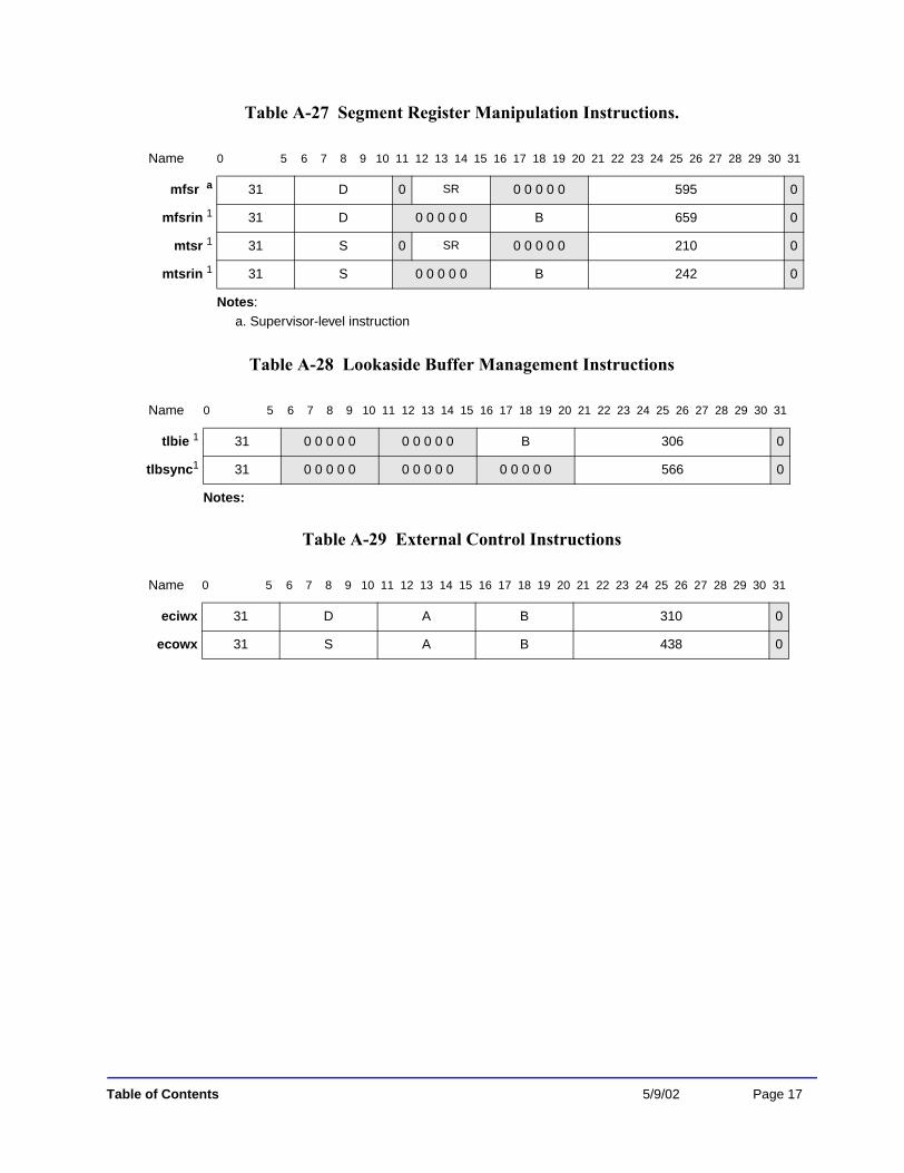
Table A-27 Segment Register Manipulation Instructions.
Table A-28 Lookaside Buffer Management Instructions
Table A-29 External Control Instructions
Name 0 5 6 7 8 9 10 11 12 13 14 15 16 17 18 19 20 21 22 23 24 25 26 27 28 29 30 31
mfsr a
a. Supervisor-level instruction
31 D 0 SR 0 0 0 0 0 595 0
mfsrin 1 31 D 0 0 0 0 0 B 659 0
mtsr 1 31 S 0 SR 0 0 0 0 0 210 0
mtsrin 1 31 S 0 0 0 0 0 B 242 0
Notes:
Name 0 5 6 7 8 9 10 11 12 13 14 15 16 17 18 19 20 21 22 23 24 25 26 27 28 29 30 31
tlbie 1 31 0 0 0 0 0 0 0 0 0 0 B 306 0
tlbsync1 31 0 0 0 0 0 0 0 0 0 0 0 0 0 0 0 566 0
Notes:
Name 0 5 6 7 8 9 10 11 12 13 14 15 16 17 18 19 20 21 22 23 24 25 26 27 28 29 30 31
eciwx 31 D A B 310 0
ecowx 31 S A B 438 0
Table of Contents 5/9/02 Page 17

Page 18 Version 1.1 IBM PowerPC 750CX/750CXe RISC Microprocessor User’s Manual
Revision Log
Rev Contents of Modification
Mar. 15, 2000 Initial preliminary release, version 1.0.
May 9, 2002 Version 1.1.Replaced a note with an implementation note in Section 12.3 ‘Dynamic Power Management” clarifying that the Dynamic Power Management (DPM) is only supported in 750CX revisions DD2.4 and DD3.1. Revised Table 2-49, Memory Synchronization Instructions. Removed references to HID2 because it is not sup-ported by the 750CX.Added a note to Table 9-8, L2 Cache Control Register concerning the reserved bits in this table.Updated the title page and the disclaimer text.
Table of Contents 5/9/02 1

2 Version 1.1 IBM PowerPC 750CX/750CXe RISC Microprocessor User’s Manual

Index
AAACK (address acknowledge) signal 7-11Absolute value instructions
floating-pointfabs, floating absolute value 12-57
Absolute value instructions, negative (fnabs) 12-73Add instructions
floating-pointfadd (double precision) 12-58fadds (single-precision) 12-59
integeradd 12-9addc, add carrying 12-10adde, add extended 12-11addi, add immediate 12-12addic, add immediate carrying 12-13addic., add immediate carrying and record 12-14addis, add immediate shifted 12-15addme, add to minus one extended 12-16addze, add to zero extended 12-17
Address busaddress tenure 8-8address transfer
An 7-4APE 8-14
address transfer attributeCI 7-10GBL 7-11TBST 7-10, 8-14TSIZn 7-9, 8-14TTn 7-6, 8-14WT 7-10
address transfer startTS 7-4, 8-13
address transfer terminationAACK 7-11ARTRY 7-12terminating address transfer 8-18
arbitration signals 7-3, 8-9bus parking 8-12
Address translation, see Memory management unitAddressing modes 2-29Algebraic instructions
lhax, load half word indexed 12-104algebraic instructions
load half word (lha) 12-101load half word with update (lhau) 12-102load half word with update indexed (lhaux) 12-103
Aligned data transfer 8-16, 8-18Alignment
data transfers 8-16
Table of Contents
exception 4-19misaligned accesses 2-23rules 2-23
An (address bus) signals 7-4and, logic instruction 12-18andc, logical and with complement instruction 12-19andi., logical and immediate instruction 12-20andis., logical and immediate shifted instruction 12-21APE (address parity error) signal 8-14Arbitration, system bus 8-10, 8-20Arithmetic instructions
floating-point 12-64–12-67, 12-71, 12-79, 12-85, 12-86, A-9
integer A-7ARTRY (address retry) signal 7-12
Bb, branch instruction 12-22bc, branch conditional instruction 12-23bcctr, branch conditional to count register 12-25bcctr, branch conditional to link register 12-27BG (bus grant) signal 7-3, 8-9Block address translation
block address translation flow 5-11definition 1-11registers
description 2-5initialization 5-19
selection of block address translation 5-8Boundedly undefined, definition 2-27BR (bus request) signal 7-3, 8-9Branch fall-through 6-18Branch folding 6-18Branch instructions
address calculation 2-49b, branch 12-22bc, branch conditional 12-23bcctr, branch conditional to count register 12-25bcctr, branch conditional to link register 12-27condition register logical 2-50, A-15description A-14list of instructions 2-49, A-14system linkage 2-51, 2-60, A-15trap 2-50, A-15
Branch prediction 6-1, 6-22Branch processing unit
branch instruction timing 6-23execution timing 6-18latency, branch instructions 6-31overview 1-8
5/9/02 Index-1

INDEX (Continued)
Branch resolutiondefinition 6-1resource requirements 6-29
BTIC (branch target instruction cache) 6-9Burst data transfers
32-bit data bus 8-3564-bit data bus 8-15transfers with data delays, timing 8-31
Bus arbitration, see Data busBus interface unit (BIU) 3-2, 8-1Bus transactions and L1 cache 3-19Byte ordering 2-29Byte reversed, load half word, indexed (lhbrx)
instruction 12-105
CCache
arbitration 6-9block instructions
dcbf, data cache block flush 12-42dcbi, data cache block invalidate 2-62, 12-43dcbst, data cache block store 12-44dcbt, data cache block touch 2-58, 12-45dcbtst, data cache block touch for store 12-46dcbz, data cache block clear to zero 12-47
block instructions, table A-16block, definition 3-3bus interface unit 3-2, 8-1cache operations
load/store operations, processor initiated 3-10operations 3-16overview 8-3
cache unit overview 3-3cache-inhibited accesses (I bit) 3-6characteristics 3-1coherency
description 3-5overview 3-22reaction to bus operations 3-23
control instructions 3-12bus operations 3-21
data cache configuration 3-3dcbf/dcbst execution 9-3hit 6-9icbi 9-3instruction cache configuration 3-4instruction cache throttling 10-10integration 3-2L1 cache and bus transactions 3-19L2 interface
cache global invalidation 9-5
Index-2 Version 1.1 IBM PowerP
cache initialization 9-4cache testing 9-6dcbi 9-3eieio 9-4operation 9-1stwcx. execution 9-3sync 9-4
load/store operations, processor initiated 3-10miss 6-14operations
cache block push operations 9-3data cache transactions 3-20instruction cache block fill 3-19snoop response to bus transactions 3-23
PLRU replacement 3-17stwcx. execution 9-3
Cache management instructionsicbi 12-87isync 12-88
Changed (C) bit maintenance recording 5-11, 5-21Checkstop
signal 7-17, 8-38state 4-18
CI (cache inhibit) signal 7-10CKSTP_IN/CKSTP_OUT(checkstop input/output)
signals 7-17Classes of instructions 2-27Clean block operation 3-23Clock signals
PLL_CFGn 7-21SYSCLK 7-20
cmp, compare instruction 12-29cmpi, compare immediate instruction 12-30cmpl, compare logical instruction 12-31cmpli, compare logical immediate instruction 12-32cntlzw, count leading zeros word instruction 12-33Compare instructions
cmp, compare 12-29cmpi, compare immediate 12-30cmpl, compare logical 12-31cmpli, compare logical immediate 12-32floating-point A-10
fcmpo, ordered compare 12-60fcmpu, unordered compare 12-61
integer A-8complement instruction (nand) 12-149complementary "or" instruction 12-153complementary or instruction (nor) 12-151Completion
completion unit resource requirements 6-30considerations 6-16definition 6-1
C 750CX/750CXe RISC Microprocessor User’s Manual

INDEX (Continued)
Condition registerinstructions
or 12-39condition register
move field instruction (mcrf) 12-120move from instruction (mfcr) 12-123move to CR from FPSCR (mcrfs) instruction 12-121move to CR from XER instruction (mcrxr) 12-122move to fields instruction (mtcrf) 12-134
Condition register instructionsand 12-34and with complement 12-35complement and 12-37complement or 12-38equivalent 12-36or with complement 12-40XOR instruction 12-41
Context synchronization 2-30Conventions 6-1Conversion instructions
fctiw, floating point to integer word 12-62fctiwz, floating point to integer word with round to
zero 12-63COP/scan interface 8-39Copy-back mode 6-27count leading zeros word (cntlzw) instruction 12-33CR (condition register)
CR logical instructions 2-50, A-15CR, description 2-3
crand, condition register and instruction 12-34crandc, condition register and with complement
instruction 12-35creqv, condition register equivalent instruction 12-36crnand, condition register complement and instruction
12-37crnor, condition register complement or instruction 12-
38cror, condition register or instruction 12-39crorc, condition register or with complement instruction
12-40crxor, condition register XOR instruction 12-41CTR register 2-4
DDABR (data address breakpoint register) 2-7DAR (data address register) 2-5Data bus
arbitration signals 7-12, 8-9bus arbitration 8-20data tenure 8-8data transfer 7-13, 8-21
Table of Contents
data transfer termination 7-15, 8-21Data cache
configuration 3-3DCFI, DCE, DLOCK bits 3-12organization 3-3
Data organization in memory 2-23Data transfers
alignment 8-16burst ordering 8-15eciwx and ecowx instructions, alignment 8-18operand conventions 2-23signals 8-21
DBG (data bus grant) signal 7-13, 8-9dcbf, data cache block flush instruction 12-42dcbi, data cache block invalidate instruction 12-43dcbst, data cache block store instruction 12-44dcbt, data cache block touch instruction 12-45dcbtst, data cache block touch for store instruction 12-
46dcbz, data cache block clear to zero instruction 12-47DEC (decrementer register) 2-6Decrementer exception 4-20Defined instruction class 2-28DHn/DLn (data bus) signals 7-13Dispatch
considerations 6-16dispatch unit resource requirements 6-29
Divide instructionsfdivs, divide (single-precision) 12-65word unsigned, divide 12-49word, divide 12-48
divw, divide word instruction 12-48divwu, divide word unsigned instruction 12-49DRTRY (data retry) signal 7-15, 8-21, 8-24DSI exception 4-18DSISR register 2-6DTLB organization 5-23Dynamic branch prediction 6-9
EEAR (external access register) 2-7eciwx, external control in word indexed instruction 12-
50ecowx, external control out word indexed instruction
12-51Effective address calculation
address translation 5-3branches 2-30loads and stores 2-30, 2-41, 2-45
eieio, enforce in-order execution of I/O 2-57, 12-52EMI protocol, enforcing memory coherency 8-25
5/9/02 Index-3

INDEX (Continued)
eqv, equivalent instruction 12-54Error termination 8-25Event counting 11-10Event selection 11-11Exceptions
alignment exception 4-19decrementer exception 4-20definitions 4-12DSI exception 4-18enabling and disabling exceptions 4-10exception classes 4-2exception prefix (IP) bit 4-12exception priorities 4-4exception processing 4-7, 4-10external interrupt 4-19FP assist exception 4-21FP unavailable exception 4-20instruction-related exceptions 2-31ISI exception 4-18machine check exception 4-16performance monitor interrupt 4-21program exception 4-19register settings
MSR 4-7, 4-12SRR0/SRR1 4-7
reset exception 4-13returning from an exception handler 4-11summary table 4-2system call exception 4-20terminology 4-1thermal management interrupt exception 4-23
Execution synchronization 2-30Execution unit timing examples 6-18Execution units 1-9External control instructions 2-60, 8-18, A-17
eciwx, external control in word indexed 12-50ecowx, external control out word indexed 12-51
extsb, extend sign byte instruction 12-55extsh, extend sign half word instruction 12-56
Ffabs, floating-point absolute value instruction 12-57fadd, floating-point add (double precision) instruction
12-58fadds, floating-point add (single-precision) instruction
12-59fcmpo, floating compare ordered 12-60fcmpu, floating compare unordered 12-61fctiw, floating convert to integer word instruction 12-62fctiwz, floating convert to integer word with round to
zero instruction 12-63
Index-4 Version 1.1 IBM PowerP
Features, list 1-4Finish cycle, definition 6-2floating point status and control register
move from instruction (mffs) 12-125move to bit 1 instruction (mtfsb1) 12-136move to field immediate instruction (mtfsfi) 12-138move to field instruction (mtfsf) 12-137
Floating-Point Execution Models—UISA 2-24Floating-point instructions
fcmpo, compare ordered 12-60fcmpu, compare unordered 12-61fdiv, divide (double-precision) 12-64fdivs, divide (single-precision) 12-65fmadd, multiply-add (double-precision) 12-66fmadds, multiply-add (single-precision) 12-67fmr, move register (double-precision) 12-68fmsub, multiply-subtract (double-precision) 12-69fmsubs, multiply-subtract (single-precision) 12-70fmul, multiply (double-precision) 12-71fmuls, multiply (single-precision) 12-72fnabs, negative absolute value 12-73fneg, negate 12-74fnmadd, negative multiply-add 12-75–??fnmadds, negative multiply-add (single-precision)
12-76fnmsub, negative multiply-subtract (double-preci-
sion) 12-77fnmsubs, negative multiply-subtract (single-preci-
sion) 12-78fres, floating reciprocal estimate (single-precision)
12-79frsp, round to single 12-81frsqrte, reciprocal square root estimate 12-82fsub, subtract (double-precision) 12-85fsubs, subtract (single-precision) 12-86lfd, load floating point (double-precision) 12-93lfdu, load floating point double word with update 12-
94lfdux, load floating- point double word with update
indexed 12-95lfdx, load floating-point double word indexed 12-96lfs, load floating-point single word 12-97lfsu, load floating point single word with update 12-98select (fsel), 12-84
Floating-point modelFE0/FE1 bits 4-9FP arithmetic instructions 2-37, 12-71, 12-85, 12-86,
A-9FP assist exceptions 4-21FP compare instructions 2-38, A-10FP divide instructions 12-64
fdivs, divide (single-precision) 12-65
C 750CX/750CXe RISC Microprocessor User’s Manual

INDEX (Continued)
FP load instructions A-13lfsux, load floating point single with update
indexed 12-99lfsx, load floating point single indexed 12-100
FP move instructions A-14FP multiply instructions 12-71FP multiply-add instructions 2-37, 12-67, A-9FP negate instructions 12-74FP operand 2-25FP rounding/conversion instructions 2-38, A-10FP store instructions 2-47, A-14FP unavailable exception 4-20FPSCR instructions 2-38, A-10IEEE-754 compatibility 2-24NI bit in FPSCR 2-25
Floating-point unitexecution timing 6-24latency, FP instructions 6-35overview 1-9
Flush block operation 3-23fmadd, floating-point multiply-add instruction 12-66fmr, move register (double-precision) 12-68fmsub, multiply-subtract (double-precision) 12-69fmsubs, multiply-subtract (single-precision) 12-70fmul, multiply (double-precision) 12-71fmuls, multiply (single-precision) 12-72fnabs, negative absolute value instruction 12-73fnmadd, negative multiply-add 12-75–??fnmsub, negative multiply-subtract (double-precision)
12-77FPRn (floating-point registers) 2-3FPSCR (floating-point status and control register)
FPSCR instructions 2-38, A-10mcrfs, move to condition register from FPSCR 12-
121FPSCR register description 2-3NI bit 2-24
fsub, subtract (double-precision) 12-85fsubs, subtract (single-precision) 12-86
GGBL (global) signal 7-11GPRn (general-purpose registers) 2-3Graphics instructions
frsqrte, square root estimate, reciprocal 12-82fsel, select 12-84stfiwx 12-175
Guarded memory bit (G bit) 3-6
Table of Contents
HHalf word instructions
lhbrx,byte reversed, load half word instruction 12-105lhz, load half word and zero 12-106lhzu, load half word and zero with update 12-107lhzux, load half word and zero with update indexed
12-108lhzx, load half word and zero indexed 12-109
HIDn (hardware implementation-dependent) registersHID0
description 2-8doze bit 10-2DPM enable bit 10-2nap bit 10-3
HID1description 2-13PLL configuration 2-13, 7-21
HRESET (hard reset) signal 7-18, 8-38
II/O execution, enforce in-order 12-52IABR (instruction address breakpoint register) 2-8icbi 12-87ICTC (instruction cache throttling control) register 2-
18, 10-11IEEE 1149.1-compliant interface 8-39Illegal instruction class 2-28immediate "or" instruction 12-154Indexed instructions
algebraic instructionslhax, load half word 12-104
lbzux, load byte and zero with update 12-91lbzx, load byte and zero 12-92lfdux, load floating-point double word with update
12-95lhbrx, byte reversed, load half word 12-105lhzux, load half word and zero with update indexed
12-108lhzx, load half word and zero 12-109load word and zero with update (lwzux) 12-118lswx, load string word 12-112lwarx, load word and reserve 12-114lwbrx, load word byte reversed 12-115lwzx, load word and zero 12-119
indexed instructionsalgebraic, load half word with update (lhaux) 12-103load floating point single (lfsx) 12-100load floating point single with update (lfsux) 12-99
Instruction cacheconfiguration 3-4instruction cache block fill operations 3-19
5/9/02 Index-5

INDEX (Continued)
organization 3-5Instruction cache throttling 10-10Instruction timing
examplescache hit 6-12cache miss 6-15
execution unit 6-18instruction flow 6-8memory performance considerations 6-27terminology 6-1
Instructionsarithmetic instructions 12-64–12-67, 12-69–12-72,
12-72–??, 12-75–12-78, 12-145–12-148branch address calculation 2-49branch instructions 6-8, 6-18, 6-20, A-14cache control instructions 9-3cache management instructions A-16
icbi 12-87isync 12-88
classes 2-27condition register logical 2-50, A-15defined instructions 2-28external control instructions 2-60, A-17floating-point
arithmetic 2-37, 12-64–12-67, 12-85, 12-86, A-9arithmetic instructions 12-79compare 2-38, A-10FP load instructions A-13FP move instructions A-14FP rounding and conversion 2-38, A-10FP status and control register 2-38FP store instructions A-14FPSCR instructions A-10multiply 12-71multiply-add 2-37, 12-67, A-9negate 12-74
fmr, move register (double-precision) 12-68fmul, multiply (double-precision) 12-71fneg, negate 12-74fsub, subtract (double-precision) 12-85fsubs, subtract (single-precision) 12-86graphics instructions 12-82, 12-84
stfiwx 12-175illegal instructions 2-28instruction cache throttling 10-10instruction flow diagram 6-10instruction serialization 6-17instruction serialization types 6-17instruction set summary 2-26integer
arithmetic 2-32, A-7compare 2-34, A-8
Index-6 Version 1.1 IBM PowerP
load A-11load/store multiple A-12load/store string A-13load/store with byte reverse A-12logical 2-34, A-8rotate and shift 2-36, A-8store A-12
integer instructions 6-33isync, instruction synchronization 4-12latency summary 6-31lfsux, load floating point single with update indexed
12-99lfsx, load floating point single indexed 12-100lha, load half word algebraic 12-101lhau, load half word algebraic with update 12-102lhaux, load half word algebraic with update indexed
12-103lnegation 12-150load 12-89–12-119load and store
address generationfloating-point 2-45integer 2-41
byte reverse instructions 2-43, A-12floating-point load A-13floating-point move 2-39, A-14floating-point store 2-46handling misalignment 2-40integer load 2-41, A-11integer multiple 2-44integer store 2-42, A-12memory synchronization 2-55, 2-56, A-13multiple instructions A-12string instructions 2-44, A-13
logic 12-149, 12-151, 12-152, 12-153, 12-154lookaside buffer management instructions A-17memory control instructions 2-57, 2-61memory synchronization instructions 2-55, 2-56, A-
13isync 12-88stwcx. 12-190sync 12-200
move 12-120–??, 12-126, 12-127, 12-130, 12-131,12-132, 12-134, 12-136, 12-137, 12-138, 12-139,12-140, 12-143, 12-144, ??–12-144
PowerPC instructions, list A-1processor control instructions 2-51, 2-56, 2-61, A-16reserved instructions 2-29rfi 4-11segment register manipulation instructions A-17stwcx. 4-12support for lwarx/stwcx. 8-39
C 750CX/750CXe RISC Microprocessor User’s Manual

INDEX (Continued)
sync 4-11system linkage instructions 2-51, A-15TLB management instructions A-17tlbie 2-63tlbsync 2-63trap instructions 2-50, A-15
INT (interrupt) signal 8-37Integer arithmetic instructions 2-32, A-7Integer compare instructions 2-34, A-8Integer load instructions 2-41, A-11Integer logical instructions 2-34, A-8Integer rotate/shift instructions 2-36, A-8Integer store gathering 6-26Integer store instructions 2-42, A-12Integer unit execution timing 6-24Interrupt, external 4-19ISI exception 4-18isync 12-88isync, instruction synchronization 2-57, 4-12ITLB organization 5-23
KKill block operation 3-23
LL2CR (L2 cache control register) 2-21, 9-4Latency
load/store instructions 6-36Latency, definition 6-2lbz, load byte and zero 12-89lbzu, load byte and zero with update instruction 12-90lbzux, load byte and zero with update indexed
instruction 12-91lbzx, load byte and zero instruction 12-92lfd, load floating point (double-precision) 12-93lfdux, load floating- point double word with update
indexed instruction 12-95lfdx, load floating-point double word instruction 12-96lfs, load floating-point single word 12-97lfsu, load floating-point single word with update 12-98lfsx, load floating point single indexed 12-100lha, load half word algebraic 12-101lhau, load half word algebraic with update 12-102lhaux, load half word algebraic with update indexed 12-
103lhax, load half word algebraic indexed 12-104lhbrx, load half word byte reversed indexed 12-105lhz, load half word and zero instruction 12-106lhzu, load half word and zero with update 12-107link register, branching to 12-27
Table of Contents
lmw, load multiple word instruction 12-110load byte and zero ( lbz) instruction 12-89load byte and zero indexed (lbzx) instruction 12-92load byte and zero with update (lbzu) instruction 12-90load byte and zero with update indexed (lbzux)
instruction 12-91Load instructions 12-89–12-119
lfdux, load floating-point double with update 12-95load multiple word (lmw) instruction 12-110load string word immediate ( lswi) instruction 12-111load word and reserve (lwarx) instruction 12-114load word and zero (lwz) instruction 12-116load word and zero indexed (lwzx) instruction 12-119load word and zero with update (lwzu) instruction 12-
117load word byte reversed (lwbrx) instruction 12-115Load/store
address generation 2-41byte reverse instructions 2-43, A-12execution timing 6-25floating-point load instructions 2-46, A-13floating-point move instructions 2-39, A-14floating-point store instructions 2-47, A-14handling misalignment 2-40integer load instructions 2-41, A-11integer store instructions 2-42, A-12latency, load/store instructions 6-36load/store multiple instructions 2-44, A-12memory synchronization instructions A-13string instructions 2-44, A-13
Logic instructionscondition register complemented XOR 12-36crand, condition register and 12-34crandc, condition register and with complement 12-
35crnand, condition register complement and 12-37crnor, condition register or complement 12-38cror, condition register or 12-39crorc, condition register or with complement 12-40crxor, condition register XOR 12-41integer
and 12-18andc, and with complement 12-19andi., and immediate 12-20
intergerandis., and immediate shifted 12-21
Logical address translation 5-1Logical instructions, integer A-8Lookaside buffer management instructions A-17LR (link register) 2-3lswi, load string word immediate instruction 12-111lswx, load string word indexed instruction 12-112
5/9/02 Index-7

INDEX (Continued)
lwarx, load word and reserve instruction 12-114lwarx/stwcx.
stwcx. 12-190lwarx/stwcx. support 8-39lwbrx, load word byte reversed instruction 12-115lwz, load word and zero instruction 12-116lwzu, load word and zero with update instruction 12-117
MMachine check exception 4-16machine state register
move from instruction (mfmsr) 12-126move to instruction (mtmsr) 12-139
MCP (machine check interrupt) signal 7-17MEI protocol
hardware considerations 3-8read operations 3-20state transitions 3-28
Memory accesses 8-6Memory coherency bit (M bit)
cache interactions 3-6timing considerations 6-27
Memory control instructionsdescription 2-57, 2-61segment register manipulation A-17
Memory management unitaddress translation flow 5-11address translation mechanisms 5-8, 5-11block address translation 5-8, 5-11, 5-19block diagrams
32-bit implementations 5-5DMMU 5-7IMMU 5-6
exceptions summary 5-15features summary 5-2implementation-specific features 5-2instructions and registers 5-17memory protection 5-10overview 5-1page address translation 5-8, 5-11, 5-26page history status 5-11, 5-20–5-22real addressing mode 5-11, 5-18segment model 5-19
Memory synchronizationisync 12-88stwcx. 12-190sync 12-200
Memory synchronization instructions 2-55, 2-56, A-13mfcr, move from condition register instruction 12-123mffs, move from floating point status and control
register instruction 12-125
Index-8 Version 1.1 IBM PowerP
mfmsr, move from machine state register instruction 12-126
mfspr, move from special purpose register instruction 12-127
mfsr, move from segmenl register instruction 12-130mfsrin, move from segment register indirect instruction
12-131mftb, move from time base register instruction 12-132Misaligned data transfer 8-37Misalignment
misaligned accesses 2-23misaligned data transfer 8-17
MMCRn (monitor mode control registers) 2-13, 4-21, 11-3
Move from instructionscondition register (mfcr) 12-123floating point and control register (mffs) 12-125machine state register (mfmsr) 12-126segment register (mfsr) 12-130segment register indirect (mfsrin) 12-131special purpose register (mfspr) 12-127time base register (mftb) 12-132
Move instructionsmcrf, move condition register field 12-120mcrfs, move to CR from FPSCR 12-121mcrxr, move to condition register from XER 12-122
Move to instructionscondition register fields (mtcrf) 12-134FPSCR bit 0 (mtfsb0) 12-135
move to instructionsFPSCR bit 1 (mtfsb1) 12-136FPSCR field immediate (mtfsfi) 12-138FPSCR fields (mtfsf) 12-137machine state register (mtmsr) 12-139segment register (mtsr) 12-143segment register, indirect (mtsrin) 12-144special purpose register (mtspr) 12-140
MSR (machine state register)bit settings 4-7FE0/FE1 bits 4-9IP bit 4-12PM bit 2-4RI bit 4-11settings due to exception 4-12
mtcrf, move to condition register fields instruction 12-134
mtfsb0, move to FPSCR bit 0 instruction 12-135mtfsb1, move to FPSCR bit 1 instruction 12-136mtfsf, move to FPSCR field instruction 12-137mtfsfi, move to FPSCR field immediate instruction 12-
138mtmsr, move to machine state register instruction 12-
C 750CX/750CXe RISC Microprocessor User’s Manual

INDEX (Continued)
139mtspr, move to special purpose register instruction 12-
140mtsr, move to segmenl register instruction 12-143mtsrin, move to segmenl register indirect instruction 12-
144Multiple-precision shifts 2-36Multiply instructions
high word (mulhw) 12-145high word unsigned (mulhwu) 12-146low word (mullw) 12-148
Multiply instructions, low immediate (mulli) 12-147Multiply-add instructions A-9
Nnand, logic instruction 12-149neg, logic instruction 12-150negative instructions
fnmadds, negative multiply-add (single-precision)12-76
fnmsubs, multiply-subtract (single-precision) 12-78nor, logic instruction 12-151
OOEA
exception mechanism 4-1memory management specifications 5-1registers 2-4
Operand conventions 2-22Operand placement and performance 6-25Operating environment architecture (OEA) 1-19Operations
bus operations caused by cache control instructions 3-21
instruction cache block fill 3-19read operation 3-20response to snooped bus transactions 3-23single-beat write operations 8-28
or, logic instruction 12-152orc, logic instruction 12-153ori, logic instruction 12-154oris 12-123, 12-125, 12-126, 12-127, 12-130, 12-131,
12-132, 12-134, 12-135, 12-136, 12-137, 12-138, 12-139, 12-140, 12-143, 12-144
Overview 1-1
PPage address translation
definition 1-11
Table of Contents
page address translation flow 5-26page size 5-19selection of page address translation 5-8, 5-14TLB organization 5-24
Page history statuscases of dcbt and dcbtst misses 5-20R and C bit recording 5-11, 5-20–5-22
Page table updates 5-32Performance monitor
event counting 11-10event selecting 11-11performance monitor interrupt 4-21, 11-1performance monitor SPRs 11-2purposes 11-1registers 11-3warnings 11-12
Phase-locked loop 10-3Physical address generation 5-1Pipeline
instruction timing, definition 6-2pipeline stages 6-7pipelined execution unit 6-4superscalar/pipeline diagram 6-4
PMC1 and PMC2 registers 1-24PMCn (performance monitor counter) registers 2-16, 4-
21, 11-5Power and ground signals 7-21Power management
doze mode 10-2doze, nap, sleep, DPM bits 2-13dynamic power management 10-1full-power mode 10-2nap mode 10-3programmable power modes 10-2sleep mode 10-4software considerations 10-5
PowerPC architectureinstruction list A-1operating environment architecture (OEA) 1-19user instruction set architecture (UISA) 1-19virtual environment architecture (VEA) 1-19
Priorities, exception 4-4Process switching 4-11Processor control instructions 2-51, 2-56, 2-61, A-16Program exception 4-19Program order, definition 6-2Programmable power states
doze mode 10-2nap mode 10-3sleep mode 10-4
Protection of memory areasno-execute protection 5-12
5/9/02 Index-9

INDEX (Continued)
options available 5-10protection violations 5-15
PVR (processor version register) 2-5
QQACK (quiescent acknowledge) signal 7-19QREQ (quiescent request) signal 7-19, 8-38Qualified bus grant 8-9Qualified data bus grant 8-20
RRead operation 3-23Read-atomic operation 3-23Read-with-intent-to-modify operation 3-23Real address (RA), see Physical address generationReal addressing mode (translation disabled)
data accesses 5-11, 5-18instruction accesses 5-11, 5-18support for real addressing mode 5-2
reciprocal estimatefloating-point (fres) 12-79
reciprocal square root estimatefloating point (frsqrte) 12-82
Record bit (Rc)description 12-3
Referenced (R) bit maintenance recording 5-11, 5-20, 5-29
Registersimplementation-specific
ICTC 2-18, 10-11L2CR 2-21, 9-4MMCR0 2-13, 4-21, 11-3MMCR1 2-15, 4-21, 11-5SIA 2-17, 4-21THRMn 2-18, 10-7UMMCR0 2-15UMMCR1 2-16UPMCn 2-17USIA 2-17
performance monitor registers 2-13SPR encodings 2-53supervisor-level
BAT registers 2-5DABR 2-7DAR 2-5DEC 2-6DSISR 2-6EAR 2-7HID0 2-8, 10-2HID1 2-13
Index-10 Version 1.1 IBM PowerP
IABR 2-8ICTC 2-18, 10-11L2CR 2-21, 9-4MMCR0 2-13, 4-21, 11-3MMCR1 2-15, 4-21, 11-5MSR 2-4PMC1 and PMC2 1-24PMCn 2-16, 4-21PVR 2-5SDR1 2-5SIA 2-17, 4-21, 11-10SPRGn 2-5SPRs for performance monitor 11-1SRn 2-5SRR0/SRR1 2-6THRMn 2-18, 10-7time base (TB) 2-6
user-levelCR 2-3CTR 2-4FPRn 2-3FPSCR 2-3GPRn 2-3LR 2-3time base (TB) 2-4, 2-6UMMCR0 2-15UMMCR1 2-16UPMCn 2-17USIA 2-17, 11-10XER 2-3
Rename buffer, definition 6-2Rename register operation 6-17Reservation station, definition 6-2Reserved instruction class 2-29Reset
HRESET signal 7-18, 8-38reset exception 4-13SRESET signal 7-18, 8-38
Retirement, definition 6-2rfi 4-11rfi (64-bit bridge) 12-157rlwimi 12-158rlwinm 12-159rlwnm 12-161Rotate/shift instructions 2-36, A-8
Ssc
user-level function 12-162SDR1 register 2-5segment register
C 750CX/750CXe RISC Microprocessor User’s Manual

INDEX (Continued)
move from indirect instruction (mfsrin) 12-131move from instruction (mfsr) 12-130move to instruction (mtsr) 12-143move to instruction (mtsrin) 12-144
Segment registersSR description 2-5SR manipulation instructions 2-62, A-17
Segmented memory model, see Memory management unit
Serializing instructions 6-17Shift/rotate instructions 2-36, A-8SIA (sampled instruction address) register 2-17, 4-21,
11-10Signals
AACK 7-11address arbitration 7-3, 8-9address transfer 8-13address transfer attribute 8-14An 7-4ARTRY 7-12, 8-21BG 7-3, 8-9BR 7-3, 8-9checkstop 8-38CI 7-10CKSTP_IN/CKSTP_OUT 7-17configuration 7-2COP/scan interface 8-39data arbitration 8-9, 8-20data transfer termination 8-21DBG 7-13, 8-9DHn/DLn 7-13DRTRY 7-15, 8-21, 8-24GBL 7-11HRESET 7-18INT 8-37MCP 7-17PLL_CFGn 7-21power and ground signals 7-21QACK 7-19QREQ 7-19, 8-38reset 8-38SRESET 7-18, 8-38system quiesce control 8-38TA 7-15TBST 7-10, 8-14, 8-21TEA 7-16, 8-21, 8-25TLBISYNC 7-19transfer encoding 7-6TS 7-4TSIZn 7-9, 8-14TTn 7-6, 8-14WT 7-10
Table of Contents
Single-beat transferreads with data delays, timing 8-29reads, timing 8-27termination 8-22writes, timing 8-28
slw 12-163Snooping 3-22special purpose register
move from instruction (mfspr) 12-127move to instruction (mtspr) 12-140
Split-bus transaction 8-9SPRGn registers 2-5sraw 12-164srawi 12-165SRESET (soft reset) signal 7-18, 8-38SRR0/SRR1 (status save/restore registers)
description 2-6exception processing 4-7
srw 12-166Stage, definition 6-2Stall, definition 6-2Static branch prediction 6-9, 6-22stb 12-167stbu 12-168stbux 12-169stbx 12-170stfd 12-171stfdu 12-172stfdux 12-173stfdx 12-174stfiwx 12-175stfs 12-176stfsu 12-177stfsux 12-178stfsx 12-179sth 12-180sthbrx 12-181sthu 12-182sthux 12-183sthx 12-184stmw 12-185Store instructions
dcbst, data cache block store 12-44string word, load immediate ( lswi) instruction 12-111string word, load indexed (lswx) instruction 12-112stswi 12-186stswx 12-187stw 12-188stwbrx 12-189stwcx. 4-12, 12-190stwcx./lwarx
stwcx. 12-190
5/9/02 Index-11

INDEX (Continued)
stwu 12-191stwux 12-192stwx 12-193subf 12-194subfc 12-195subfe 12-196subfic 12-197subfme 12-198subfze 12-199Superscalar, definition 6-3sync 4-11, 12-200SYNC operation 3-23Synchronization
context/execution synchronization 2-30execution of rfi 4-11memory synchronization instructions 2-55, 2-56, A-
13SYSCLK (system clock) signal 7-20System call exception 4-20System linkage instructions 2-51, 2-60
list of instructions A-15rfi 12-157sc 12-162
System quiesce control signals (QACK/ QREQ) 8-38System register unit
execution timing 6-26latency, CR logical instructions 6-32latency, system register instructions 6-31
TTA (transfer acknowledge) signal 7-15Table search flow (primary and secondary) 5-29TBL/TBU (time base lower and upper) registers 2-4, 2-6TBST (transfer burst) signal 7-10, 8-14, 8-21TEA (transfer error acknowledge) signal 7-16, 8-25Termination 8-18, 8-21Thermal assist unit (TAU) 10-5Thermal management interrupt exception 4-23THRMn (thermal management) registers 2-18, 10-7Throughput, definition 6-3time base register
move from instructions (mftb) 12-132Timing diagrams, interface
address transfer signals 8-13burst transfers with data delays 8-31single-beat reads 8-27single-beat reads with data delays 8-29single-beat writes 8-28single-beat writes with data delays 8-30use of TEA 8-32
Timing, instruction
Index-12 Version 1.1 IBM PowerP
BPU execution timing 6-18branch timing example 6-23cache hit 6-12cache miss 6-15execution unit 6-18FPU execution timing 6-24instruction dispatch 6-16instruction flow 6-8instruction scheduling guidelines 6-28IU execution timing 6-24latency summary 6-31load/store unit execution timing 6-25SRU execution timing 6-26stage, definition 6-2
TLBdescription 5-22invalidate (tlbie instruction) 5-26, 5-32LRU replacement 5-25organization for ITLB and DTLB 5-23TLB miss and table search operation 5-25, 5-28
TLB invalidatedescription 5-26TLB management instructions 2-63, A-17
TLB miss, effect 6-28tlbie 2-63, 12-201TLBISYNC (TLBI sync) signal 7-19tlbsync 2-63, 12-202Touch instructions
dcbt, data cache block touch 12-45dcbtst, data cache block touch for store 12-46
Transactions, data cache 3-20Transfer 8-13, 8-21Trap instructions 2-50TS (transfer start) signal 7-4, 8-13TSIZn (transfer size) signals 7-9, 8-14TTn (transfer type) signals 7-6, 8-14tw 12-203twi 12-204two’s complement instruction (neg) 12-150
UUMMCR0 (user monitor mode control register 0) 2-15,
11-5UMMCR1 (user monitor mode control register 1) 2-16,
11-5UPMCn (user performance monitor counter) registers
2-17, 11-9Use of TEA, timing 8-32User instruction set architecture (UISA)
description 1-19registers 2-3
C 750CX/750CXe RISC Microprocessor User’s Manual

INDEX (Continued)
USIA (user sampled instruction address) register 2-17, 11-10
VVirtual environment architecture (VEA) 1-19
WWIMG bits 8-25word unsigned, divide (divwu) instruction 12-49word, divide (divw) instruction 12-48Write-back, definition 6-3Write-through mode (W bit)
cache interactions 3-6Write-with-Atomic operation 3-23Write-with-Flush operation 3-23Write-with-Kill operation 3-23WT (write-through) signal 7-10
XXER register 2-3xor 12-205xori 12-206xoris 12-207
Table of Contents
5/9/02 Index-13