I P J M J. Micromech. Microeng. 15 (2005) 2105–2112 ... · Characterization of high-Q spiral...
8
INSTITUTE OF PHYSICS PUBLISHING JOURNAL OF MICROMECHANICS AND MICROENGINEERING J. Micromech. Microeng. 15 (2005) 2105–2112 doi:10.1088/0960-1317/15/11/016 Characterization of high-Q spiral inductors on thick insulator-on-silicon Mina Rais-Zadeh and Farrokh Ayazi School of Electrical and Computer Engineering, Georgia Institute of Technology, Atlanta, GA 30332-0250, USA Received 14 June 2005, in final form 16 August 2005 Published 23 September 2005 Online at stacks.iop.org/JMM/15/2105 Abstract This paper reports on the fabrication and characterization of high quality factor (Q) copper (Cu) inductors with thick insulator on standard silicon (Si) substrate (ρ = 10–20 cm). The thickness and the area of the insulating layer are optimized for high Q by fabricating inductors on very thick (∼50 µm) embedded silicon dioxide (SiO 2 ) islands and 4–20 µm thick PECVD SiO 2 coated standard Si substrate. The effect of the dielectric permittivity is verified by comparing the performances of identical inductors fabricated on 20 µm thick SiO 2 and 20 µm thick low-k polymer coated standard Si substrate. Measurement results show saturation behavior for the inductor Q versus the area and the thickness of the insulating layer. A 0.9 nH inductor fabricated on a 50 µm thick embedded oxide island (OI) exhibits a high peak Q of 53 at 2 GHz. The Q of an identical inductor on 20 µm thick PECVD SiO 2 is 45 at 2 GHz. (Some figures in this article are in colour only in the electronic version) 1. Introduction High-Q integrated inductors are widely used to improve the performance of advanced RF integrated circuits such as voltage-controlled oscillators [1], low noise amplifiers [2], power amplifiers [3], mixers, filters and matching networks. The quality factor of on-chip inductors is limited by the loss mechanisms that convert the electromagnetic energy into heat. There are two separate sources of loss in inductors: the metal loss and the substrate loss. Therefore, the unloaded Q of an inductor can be expressed by [4]: 1 Q = 1 Q substrate + 1 Q metal , (1) where Q substrate and Q metal represent the substrate loss and the Ohmic loss of metal strips, respectively. While metal loss can be reduced by using thick high-conductivity metals, the loss of Si substrate has remained the major barrier in reaching Q’s comparable to that of off-chip inductors. Micromachining techniques have been utilized to improve the Q substrate . Approaches taken to reduce the substrate loss and increase the Q can be summarized as the use of a thick insulating layer, whether by suspension of the inductor [5–7] or by the use of a thick dielectric [8–10]. The substrate loss is known to decrease with increasing thickness of the insulating layer [11, 12]. However, there is a saturation thickness for the dielectric beyond which the Q remains constant. On the other hand, the electromagnetic field produced by the current flowing in the inductor vanishes in the close vicinity of the edge of the inductor (tens of microns), resulting in saturation behavior for the inductor Q versus the area of the insulating layer (figure 1). This saturation behavior alleviates the need to insulate the entire area beneath the inductor. This is of special importance when an upper limit exists on the area of the insulating layer due to the processing constraints. Very little work has been done so far to characterize and optimize the dielectric saturation thickness and area [13]. This paper investigates the effect of the thickness, area and the permittivity of the insulating layer on the inductor performance. The thickness and the area of the insulating layer are characterized by fabricating several spiral-type inductors on thick embedded SiO 2 as well as on thick PECVD SiO 2 coated standard Si substrate. The saturation thickness and the optimum area of the insulating layer are extracted from the measurement results. To investigate the effect of the substrate permittivity, the performances of inductors fabricated on 20 µm thick PECVD SiO 2 and 20 µm thick low-k polymer coated standard Si substrate are compared. Experimental results are in excellent agreement with Sonnet electromagnetic simulations [14]. 0960-1317/05/112105+08$30.00 © 2005 IOP Publishing Ltd Printed in the UK 2105
Transcript of I P J M J. Micromech. Microeng. 15 (2005) 2105–2112 ... · Characterization of high-Q spiral...
INSTITUTE OF PHYSICS PUBLISHING JOURNAL OF MICROMECHANICS AND MICROENGINEERING
J. Micromech. Microeng. 15 (2005) 2105–2112 doi:10.1088/0960-1317/15/11/016
Characterization of high-Q spiralinductors on thick insulator-on-siliconMina Rais-Zadeh and Farrokh Ayazi
School of Electrical and Computer Engineering, Georgia Institute of Technology, Atlanta,GA 30332-0250, USA
Received 14 June 2005, in final form 16 August 2005Published 23 September 2005Online at stacks.iop.org/JMM/15/2105
AbstractThis paper reports on the fabrication and characterization of high qualityfactor (Q) copper (Cu) inductors with thick insulator on standard silicon (Si)substrate (ρ = 10–20 � cm). The thickness and the area of the insulatinglayer are optimized for high Q by fabricating inductors on very thick(∼50 µm) embedded silicon dioxide (SiO2) islands and 4–20 µm thickPECVD SiO2 coated standard Si substrate. The effect of the dielectricpermittivity is verified by comparing the performances of identical inductorsfabricated on 20 µm thick SiO2 and 20 µm thick low-k polymer coatedstandard Si substrate. Measurement results show saturation behavior for theinductor Q versus the area and the thickness of the insulating layer. A0.9 nH inductor fabricated on a 50 µm thick embedded oxide island (OI)exhibits a high peak Q of 53 at 2 GHz. The Q of an identical inductor on20 µm thick PECVD SiO2 is 45 at 2 GHz.
(Some figures in this article are in colour only in the electronic version)
1. Introduction
High-Q integrated inductors are widely used to improvethe performance of advanced RF integrated circuits such asvoltage-controlled oscillators [1], low noise amplifiers [2],power amplifiers [3], mixers, filters and matching networks.The quality factor of on-chip inductors is limited by the lossmechanisms that convert the electromagnetic energy into heat.There are two separate sources of loss in inductors: the metalloss and the substrate loss. Therefore, the unloaded Q of aninductor can be expressed by [4]:
1
Q= 1
Qsubstrate+
1
Qmetal, (1)
where Qsubstrate and Qmetal represent the substrate loss andthe Ohmic loss of metal strips, respectively. While metalloss can be reduced by using thick high-conductivity metals,the loss of Si substrate has remained the major barrierin reaching Q’s comparable to that of off-chip inductors.Micromachining techniques have been utilized to improvethe Qsubstrate. Approaches taken to reduce the substrateloss and increase the Q can be summarized as the use of athick insulating layer, whether by suspension of the inductor[5–7] or by the use of a thick dielectric [8–10]. The substrateloss is known to decrease with increasing thickness of theinsulating layer [11, 12]. However, there is a saturation
thickness for the dielectric beyond which the Q remainsconstant. On the other hand, the electromagnetic fieldproduced by the current flowing in the inductor vanishes inthe close vicinity of the edge of the inductor (tens of microns),resulting in saturation behavior for the inductor Q versus thearea of the insulating layer (figure 1). This saturation behavioralleviates the need to insulate the entire area beneath theinductor. This is of special importance when an upper limitexists on the area of the insulating layer due to the processingconstraints.
Very little work has been done so far to characterizeand optimize the dielectric saturation thickness and area[13]. This paper investigates the effect of the thickness, areaand the permittivity of the insulating layer on the inductorperformance. The thickness and the area of the insulating layerare characterized by fabricating several spiral-type inductorson thick embedded SiO2 as well as on thick PECVD SiO2
coated standard Si substrate. The saturation thickness and theoptimum area of the insulating layer are extracted from themeasurement results. To investigate the effect of the substratepermittivity, the performances of inductors fabricated on20 µm thick PECVD SiO2 and 20 µm thick low-k polymercoated standard Si substrate are compared. Experimentalresults are in excellent agreement with Sonnet electromagneticsimulations [14].
0960-1317/05/112105+08$30.00 © 2005 IOP Publishing Ltd Printed in the UK 2105
M Rais-Zadeh and F Ayazi
t ox
dox
t ox
dox
w
s
t metal
Si
insulator
d out
t ox
dox
t ox
dox
ws
t metal
Si
insulator
d out
Figure 1. Inductor schematic showing the electromagnetic field.
2. Fabrication
To characterize the effect of the insulating layer on the inductorQ, three types of thick insulating layers are created on andin the Si substrate using micromachining techniques: thickembedded oxide islands, thick PECVD SiO2 and thick Avatrelpolymer [15]. Planar Cu inductors are then fabricated on thesepre-processed substrates using the surface micromachiningtechnique introduced in [9].
2.1. Thick embedded oxide islands
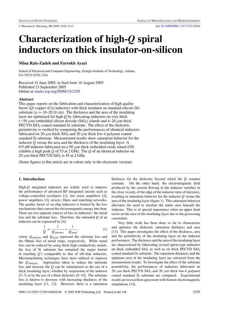
In the main approach, a bulk micromachining technique isutilized to create very thick embedded oxide islands (OI) inthe standard Si substrate (ρ = 10–20 � cm). The embeddedOI is realized by etching deep high aspect-ratio (25:1) trenchesin select areas of the Si substrate and subsequently oxidizingthe Si left in between the trenches at 950 ◦C [16, 17]. 2 µmthick PECVD SiO2 is then deposited at 300 ◦C to improvethe surface roughness. A brief fabrication process flow ofinductors on thick embedded oxide islands is shown in figure 2.Figure 3 shows a 50 µm thick embedded OI with repeatedtrench and Si width of about 2 µm.
To have a void-free solid oxide island, the ratio of thetrench width to the Si width should be 1:0.818. Insufficientspacing between the Si bars results in early closing of thetrenches before the Si bar is fully oxidized. Continuing theoxidation process in this case causes curvature in the waferdue to the stress introduced by oxidation of the remainingSi bars. To reduce the curvature of each individual Si barduring the oxidation process, the length of the bar is reducedby introducing multiple rows and shifting the trench profile ofeach row with respect to the adjacent row, as shown in figure 4.Using this trench profile, low-stress oxide islands of large areas(3 mm × 3 mm) have been achieved.
The stress in the oxidized Si bars, which in the extremecase causes curving of the wafer, is also dependent on theoxidation temperature. Figure 5(a) shows a highly stressed OIbefore full oxidation of Si, when the wet oxidation temperaturewas 1100 ◦C. For comparison, the SEM picture of a low-stressOI processed at 950 ◦C is shown in figure 5(b). The trenchprofile and the processing parameters become critical when alarge percentage of the wafer area is trenched. Therefore, theoxide island area is an important design parameter that needsto be optimized and was not studied in earlier work [7, 8].Figure 6 shows the cross-section SEM view of a multiple-turn
(d )
(e)
(a) (b)
(c)
Figure 2. Fabrication process flow of inductors on oxide islands.(a) Etching deep trenches in Si, (b) oxidizing the remaining Si,(c) depositing and patterning the first metal layer, (d) depositing andpatterning the interlayer dielectric and (e) electroplating the secondmetal layer.
copper inductor fabricated on a 50 µm thick embedded OI.Thick Cu (∼20 µm) is electroplated to increase the Qmetal andreduce the effect of metal loss on the inductor performance.
2.2. Thick PECVD SiO2 coated Si
Although the thick embedded OI has a significant effect onthe reduction of the Si substrate loss, the high processingtemperature makes it incompatible for post-CMOS processing[8]. The alternative low-temperature approach to create a thickoxide layer is PECVD SiO2 deposition at 300 ◦C with a typicaldeposition rate of 4 µm h−1. The SiO2 film thickness that canbe deposited using the PECVD process is limited, due to thethermal stress introduced between the thick SiO2 layer and the
2106

Characterization of high-Q spiral inductors on thick insulator-on-silicon
PECVD oxide
Thermal oxide
Figure 3. SEM views of a 50 µm thick oxide island showing thesmooth surface (oxidation temperature: 950 ◦C).
Si
Trench
Figure 4. Microscope picture of the trenched area, showing theposition of each Si bar with respect to adjacent bars.
Si substrate. To lower the thermal stress in this work, a 20 µmthick oxide layer is created by repeated deposition of a 4 µmthick oxide layer. Figure 7 shows SEM pictures of a 3.3 nHinductor on a 20 µm thick SiO2 coated Si substrate.
2.3. Thick low-k polymer coated Si
To study the effect of the dielectric permittivity, inductors arealso fabricated on a 20 µm thick low-k polymer spin coated onstandard Si substrate. Avatrel 2000P polymer from PromerousInc. has been selected for this purpose as it has a low dielectricpermittivity compared to other dielectric materials [15].Table 1 compares the electrical properties of Avatrel with twoother low-k dielectrics commonly used as insulating layers,showing the small relative permittivity and loss-tangent of thismaterial [18]. Following the spin-coating, the Avatrel polymeris cured at 110 ◦C and 1 µm thick SiO2 is deposited at 160 ◦Cto promote the adhesion of successive metallic layers to thepolymer. The deposition temperature of SiO2 is reduced (from300 ◦C to 160 ◦C) to avoid bubbling of the Avatrel.
(a)
(b)
Figure 5. (a) Cross-section SEM view of a highly stressed oxideisland (oxidation temperature: 1100 ◦C), and (b) top view of a lowstressed OI (oxidation temperature: 950 ◦C).
Table 1. Comparison of electrical properties of Avatrel with BCBand polyimide [18].
Avatrel Polyimide BCB
tan δ at 1 GHz 0.009 0.01–0.015 0.015Permittivity (εr) 2.55 3.1–4.1 2.7Moisture uptake <0.1% 0.5–3% 0.23%
3. Measured results and discussion
Several spiral-type inductors of various shapes and dimensionswere fabricated and tested on 50 µm thick OI, 4–20 µmthick PECVD SiO2 and 20 µm thick Avatrel coated standardSi substrate (ρ = 10–20 � cm). On-wafer S-parametermeasurements were carried out using an hp8517B vectornetwork analyzer and ground–signal–ground Cascade micro-probes. The pad-only characteristics were measured on the
2107

M Rais-Zadeh and F Ayazi
Oxide Island
Figure 6. SEM picture of a three-turn inductor on top of OI(w = 15 µm, dout = 300 µm, tmetal = 20 µm).
(a)
(b)
SiO2 layer
Figure 7. (a) Cross-section and (b) top SEM view of a 3.3 nH Cuinductor on 20 µm thick PECVD SiO2 (tmetal = 1.5 µm, n = 2.5,w = 20 µm, s = 20 µm and dout = 400 µm).
open pad structures and de-embedded from the overall inductorcharacteristic by subtracting the Y-parameters of the pads fromthe Y-parameters of the embedded inductors [19].
0
10
20
30
40
50
60
0 2 4 6 8 10 12Frequency (GHz)
Qua
lity
fact
or
(a)
0
10
20
30
40
50
60
0 20 40 60 80 100 120
Oxide thickness (µm)
Qua
lity
fact
or
(b)
(c)
7µm PECVD SiO2
4 µm PECVD SiO2
20 µm PECVD SiO2
Simulated (Sonnet)
Un-oxidized Si
Measureddata points
Figure 8. (a) Measured Q of a 1 nH inductor with various oxidethicknesses, (b) comparison of simulated and measured Q at4 GHz and (c) cross-section SEM picture of OI showing theincomplete oxidation of Si (tmetal = 20 µm, w = 60 µm,dout = 600 µm).
Figure 8(a) shows the Q of a one-turn 1 nH inductor withvarious oxide thicknesses. The similar performance observedin the low frequency range (f < 2 GHz) is due to the metalloss limitation on the Q [4, 9]. At higher frequencies, wherethe substrate loss is dominant, Q increases with increasingoxide thickness. Figure 8(b) compares the simulated andthe measured Q of this inductor at 4 GHz, showing excellentagreement for oxide thickness of up to 20 µm. The deviationof the measured Q value from the simulated Q for the inductoron 50 µm thick OI is due to the incomplete oxidation of Si(figure 8(c)). On account of the agreement observed betweensimulations and measurements, inductors were not fabricatedon thicker oxide islands.
2108
Characterization of high-Q spiral inductors on thick insulator-on-silicon
(a) (b) (c)
tox=50µm J=1.97e-4
tox=100µm J=0.834e-4
tox=1µm J=7.3e-3
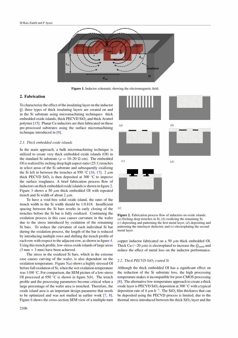
Figure 9. Current density at the common surface of oxide and Si for an inductor fabricated on (a) 1 µm, (b) 50 µm and (c) 100 µm thickoxide coated standard Si substrate at 5 GHz (tmetal = 20 µm, w = 60 µm, dout = 600 µm).
(a)
0
5
10
15
20
25
30
35
0 2 4 6 8 10
Frequency (GHz)
Qua
lity
fact
or
(b)
X=300 µm
X=0 µm
X=50 µm
X
Oxide Island area
X
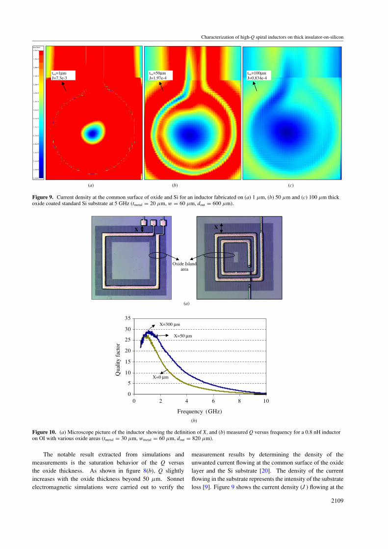
Figure 10. (a) Microscope picture of the inductor showing the definition of X, and (b) measured Q versus frequency for a 0.8 nH inductoron OI with various oxide areas (tmetal = 30 µm, wmetal = 60 µm, dout = 820 µm).
The notable result extracted from simulations andmeasurements is the saturation behavior of the Q versusthe oxide thickness. As shown in figure 8(b), Q slightlyincreases with the oxide thickness beyond 50 µm. Sonnetelectromagnetic simulations were carried out to verify the
measurement results by determining the density of theunwanted current flowing at the common surface of the oxidelayer and the Si substrate [20]. The density of the currentflowing in the substrate represents the intensity of the substrateloss [9]. Figure 9 shows the current density (J ) flowing at the
2109
M Rais-Zadeh and F Ayazi
Width of the metal
X=50µm J= 2.25e-3
X=100µm J=3.21e-4
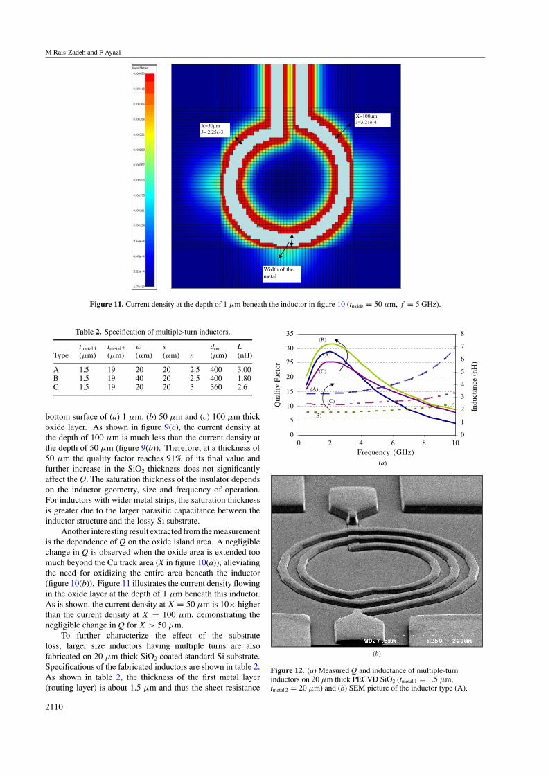
Figure 11. Current density at the depth of 1 µm beneath the inductor in figure 10 (toxide = 50 µm, f = 5 GHz).
Table 2. Specification of multiple-turn inductors.
tmetal 1 tmetal 2 w s dout LType (µm) (µm) (µm) (µm) n (µm) (nH)
A 1.5 19 20 20 2.5 400 3.00B 1.5 19 40 20 2.5 400 1.80C 1.5 19 20 20 3 360 2.6
bottom surface of (a) 1 µm, (b) 50 µm and (c) 100 µm thickoxide layer. As shown in figure 9(c), the current density atthe depth of 100 µm is much less than the current density atthe depth of 50 µm (figure 9(b)). Therefore, at a thickness of50 µm the quality factor reaches 91% of its final value andfurther increase in the SiO2 thickness does not significantlyaffect the Q. The saturation thickness of the insulator dependson the inductor geometry, size and frequency of operation.For inductors with wider metal strips, the saturation thicknessis greater due to the larger parasitic capacitance between theinductor structure and the lossy Si substrate.
Another interesting result extracted from the measurementis the dependence of Q on the oxide island area. A negligiblechange in Q is observed when the oxide area is extended toomuch beyond the Cu track area (X in figure 10(a)), alleviatingthe need for oxidizing the entire area beneath the inductor(figure 10(b)). Figure 11 illustrates the current density flowingin the oxide layer at the depth of 1 µm beneath this inductor.As is shown, the current density at X = 50 µm is 10× higherthan the current density at X = 100 µm, demonstrating thenegligible change in Q for X > 50 µm.
To further characterize the effect of the substrateloss, larger size inductors having multiple turns are alsofabricated on 20 µm thick SiO2 coated standard Si substrate.Specifications of the fabricated inductors are shown in table 2.As shown in table 2, the thickness of the first metal layer(routing layer) is about 1.5 µm and thus the sheet resistance
0
5
10
15
20
25
30
35
0 2 4 6 8 10Frequency (GHz)
Qua
lity
Fact
or
0
1
2
3
4
5
6
7
8
Indu
ctan
ce (
nH)
(a)
(b)
(A)
(B)
(C)
(A)
(B)
(C)
Figure 12. (a) Measured Q and inductance of multiple-turninductors on 20 µm thick PECVD SiO2 (tmetal 1 = 1.5 µm,tmetal 2 = 20 µm) and (b) SEM picture of the inductor type (A).
2110

Characterization of high-Q spiral inductors on thick insulator-on-silicon
0
10
20
30
40
50
0 2 4 6 8 10
Frequency (GHz)
Qua
lity
fact
or
(a)
0
10
20
30
40
50
60
0 2 4 6 8 10Frequency (GHz)
Qua
lity
fact
or
(b)
20 µm thick Avatrel, εr =2.5
20 µm thick SiO2, εr=3.9
20 µm thick Avatrel, εr =2.5
20 µm thick SiO2, εr =3.9
Figure 13. (a) Measured Q of identical inductors on 20 µm thickoxide and 20 µm thick Avatrel coated standard Si substrate(a) w = 50 µm, dout = 500 µm, tmetal = 20 µm, and (b) w =60 µm, dout = 600 µm, tmetal = 20 µm.
of the first metal layer is about 13 times higher than that ofthe second metal layer. Although the first metal layer is verythin, the quality factor of the multiple-turn inductors is lowerthan the single-turn inductors due to the Ohmic loss of the firstmetal layer. Figure 12 compares the performances of inductortypes A, B and C. The following has been extracted from themeasured data shown in figure 12:
(1) Comparison of inductors A and B shows that inductorswith wider metals have higher Q but lower inductance[21].
(2) Smaller size inductors have superior performance athigher frequencies due to their lower substrate loss(inductor A compared to inductor C).
The effect of the insulating layer permittivity is alsoverified. Figure 13 shows the measured Q of two differenttypes of inductors fabricated on 20 µm thick oxide and20 µm thick Avatrel coated Si substrate. At high frequencies(f > 4 GHz), Q of inductors on Avatrel is higher due to theirreduced substrate loss. As shown in figure 13(b), the peakQ of a 0.9 nH inductor is 52 at 2 GHz when the Si substrateis passivated with 20 µm thick Avatrel, while the Q of theexact same inductor fabricated on 20 µm thick oxide is 45 at2 GHz.
4. Conclusion
High-Q integrated Cu inductors were fully characterized onthick insulator on Si. Thick oxide islands were employed tocharacterize the effect of the dielectric area on the inductorperformance. Measurement results show saturation behaviorfor the inductor Q versus the dielectric area. For one-turninductors, negligible change in Q was observed when theoxide area was extended beyond 50 µm from the edge ofthe inductor. On the other hand, the optimum value of theinsulator thickness was obtained by fabricating the inductorson thick PECVD oxide and oxide islands. It was foundthat the oxide thickness required to effectively reduce theSi loss depends on the inductor geometry and size, and wasabout 50 µm in this work. The measurement results wereverified by Sonnet electromagnetic simulations. The effectof the insulator permittivity on the quality factor of on chipinductors was studied by fabrication of identical inductorson 20 µm thick low-k polymer and 20 µm thick PECVDoxide. Measurement results show superior performance forinductors fabricated on low-k insulating layer due to theirreduced substrate loss.
Acknowledgments
This work was supported by NSF through the PackagingResearch Center (PRC) at Georgia Tech. The authors wouldlike to thank the staff at the Georgia Tech MicroelectronicsResearch Center for their assistance, Reza Abdolvand forvaluable discussions and Pejman Monajemi for help withfabrication.
References
[1] Yoon S W, Pinel S and Laskar J 2005 A 0.35-µm CMOS2-GHz VCO in wafer-level package IEEE Microw. Wirel.Compon. Lett. 15 229–31
[2] Jeong Y, Doh H, Jung S, Park D S-W and Lee J-B 2004CMOS VCO and LNA implemented by air-suspendedon-chip RF MEMS LC 47th Midwest Symp. on Circuits andSystems, MWSCAS ’04 (Japan, July 2004) vol 1 pp I-373–6
[3] Burghartz J N, Soyuer M, Jenkins K A and Hulvey M D 1995High-Q inductors in standard silicon interconnecttechnology and its application to an integrated RF poweramplifier IEEE Int. Electron Device Meeting (Washington,DC) pp 1015–7
[4] Arcioni P, Castello R, Perregrini L, Sacchi E and Svelto F1999 An innovative modelization of loss mechanism insilicon integrated inductor IEEE Trans. Circuits Syst. II 461453–60
[5] Yoon J-B, Seok Choi Y, Kim B and Yoon E 2002CMOS-compatible surface-micromachined suspended-spiral inductors for multi-GHz silicon RF ICs IEEEElectron. Device Lett. 23 591–3
[6] Lakdawala H, Zhu X, Santhanam S, Carley L R andFedder G K 2002 Micromachined high-Q inductors in a0.18 µm copper interconnect low-k dielectric CMOSprocess IEEE J. Solid-State Circuits 37 394–403
[7] Jiang H, Wang Ye, Yeh J A and Tien N C 2000 On-chip spiralinductors suspended over deep copper-lined cavities IEEETrans. Microw. Theory Tech. 48 2415–23
[8] Erzgraber H B, Grabolla Th, Richter H H, Schley P andWolff A 1998 A novel buried oxide isolation for monolithicRF inductors on silicon IEEE Int. Electron Device Meeting(San Francisco, CA) pp 535–9
2111
M Rais-Zadeh and F Ayazi
[9] Raieszadeh M, Monajemi P, Yoon S, Laskar J and Ayazi F2005 High-Q integrated inductors on trenched Si islandsIEEE Int. Conf. on Microelectromechanical Systems(Miami, USA, Jan. 2005) pp 199–202
[10] Huo X, Chen K J and Chan P C H 2002 Silicon-basedhigh-Q inductors incorporating electroplated copper andlow-k BCB dielectric IEEE Electron. Device Lett.23 520–2
[11] Ribas R P, Lescot J, Leclercq J-L, Karam J M andNdagijimana F 2000 Physical modeling of spiral inductorson silicon IEEE Trans. Electron. Devices 47 560–8
[12] Lu E H, Ponchak G E, Bhattacharya P and Katehi L P B 2000Micromachined microwave planar spiral inductors andtransformers IEEE Trans. Microw. Theory Tech. 48 1326–35
[13] Zheng D, Becker A, Xie Y and Kim H 2001 Spiral inductorson Si p/p+ substrates with resonant frequency of 20 GHzIEEE Electron. Device Lett. 22 275–7
[14] http://www.sonnetusa.com[15] http://www.promerus.com
[16] Wang G, Bacon A, Abdolvand R, Ayazi F, Papapolymerou Jand Tentzeris E M 2003 Finite ground coplanar lines onCMOS grade silicon with a thick embedded silicon oxidelayer using micromachining techniques 33rd EuropeanMicrowave Conf. (Munich, Germany, Oct. 2003) pp 25–7
[17] Jiang H, Yoo1 K, Yeh J, Li Z and Tien N 2002 Fabrication ofthick silicon dioxide sacrificial and isolation blocks in asilicon substrate J. Micromech. Microeng. 12 87–95
[18] Patel K S, Kohl P A and Bidstrup-Allen S A 2001Three-dimensional dielectric characterization of polymerfilms J. Appl. Polym. Sci. 80 2328–34
[19] Wartenberg S A 2002 De-embedding the pads andinterconnects RF Measurement of Die and Packaging(Norwood, MA: Artech House) section 6.3, pp 118–31
[20] Rautio J C 1999 Free EM simulator analyzes spiral inductorson silicon Microw. RF Mag. 165–72
[21] Long J R and Copeland M A 1997 The modeling,characterization, and design of monolithic inductors forsilicon RF IC’s IEEE J. Solid-State Circuits 32 357–69
2112