
J. Micromech. Microeng. 19 (2009) 075008 (7pp) Dual-side ...
7
IOP PUBLISHING JOURNAL OF MICROMECHANICS AND MICROENGINEERING J. Micromech. Microeng. 19 (2009) 075008 (7pp) doi:10.1088/0960-1317/19/7/075008 Dual-side and three-dimensional microelectrode arrays fabricated from ultra-thin silicon substrates Jiangang Du 1 , Michael L Roukes 2 and Sotiris C Masmanidis 1 1 Department of Computation and Neural Systems, Division of Biology, California Institute of Technology, Pasadena, CA 91125, USA 2 Kavli Nanoscience Institute, California Institute of Technology, Pasadena, CA 91125, USA E-mail: [email protected] Received 2 April 2009 Published 23 June 2009 Online at stacks.iop.org/JMM/19/075008 Abstract A method for fabricating planar implantable microelectrode arrays was demonstrated using a process that relied on ultra-thin silicon substrates, which ranged in thickness from 25 to 50 μm. The challenge of handling these fragile materials was met via a temporary substrate support mechanism. In order to compensate for putative electrical shielding of extracellular neuronal fields, separately addressable electrode arrays were defined on each side of the silicon device. Deep reactive ion etching was employed to create sharp implantable shafts with lengths of up to 5 mm. The devices were flip-chip bonded onto printed circuit boards (PCBs) by means of an anisotropic conductive adhesive film. This scalable assembly technique enabled three-dimensional (3D) integration through formation of stacks of multiple silicon and PCB layers. Simulations and measurements of microelectrode noise appear to suggest that low impedance surfaces, which could be formed by electrodeposition of gold or other materials, are required to ensure an optimal signal-to-noise ratio as well a low level of interchannel crosstalk. (Some figures in this article are in colour only in the electronic version) 1. Introduction Microfabrication technology promises to significantly enhance the quality of in vivo electrophysiological measurements of neuronal activity in terms of spatial resolution, topographical precision and single-cell yield [1, 2]. Microelectromechanical systems (MEMS) offer a high degree of control over electrode position and spacing, and the possibility for integration with electronics [3], drug delivery channels [4], and electrical stimulation sites [5]. MEMS neural probes containing around 100 recording sites have already provided glimpses of the rich dynamics of rodent neurophysiological activity with single cell and spike time accuracy [6]. The design of such probes has primarily focused on providing planar (i.e., two-dimensional, 2D) information. But the immense complexity of neuronal circuitry suggests the development of volumetric (i.e., 3D) electrophysiological recording tools enabling high-resolution measurements of activity within and between multiple cortical regions. A growing number of different MEMS neural probes have been demonstrated, with a variety of electrode geometries, substrate materials, and methods for fabrication and assembly. Many are inspired by the planar microelectrode architecture [7], which contains multiple electrodes arranged in a single plane, distributed on one or more sharp implantable shafts. An alternative architecture is embodied in the intracortical array [8]. This configuration samples extracellular fields from the tip of each shaft, and though the tips are not confined to a single plane, prospects for dense 3D recording appear limited, as there is only one electrode per shaft. Recent efforts at realizing true 3D recording functionality have begun to show promise [9–12], but the widespread use of those devices appears to remain limited. This paper presents an alternative method for developing silicon-based neural probes aimed at high single-unit yield, high spatial resolution extracellular measurements. We developed a process for fabricating devices from ultra-thin silicon substrates. Our process shares some similarities 0960-1317/09/075008+07$30.00 1 © 2009 IOP Publishing Ltd Printed in the UK
Transcript of J. Micromech. Microeng. 19 (2009) 075008 (7pp) Dual-side ...
IOP PUBLISHING JOURNAL OF MICROMECHANICS AND MICROENGINEERING
J. Micromech. Microeng. 19 (2009) 075008 (7pp) doi:10.1088/0960-1317/19/7/075008
Dual-side and three-dimensionalmicroelectrode arrays fabricated fromultra-thin silicon substratesJiangang Du1, Michael L Roukes2 and Sotiris C Masmanidis1
1 Department of Computation and Neural Systems, Division of Biology, California Institute ofTechnology, Pasadena, CA 91125, USA2 Kavli Nanoscience Institute, California Institute of Technology, Pasadena, CA 91125, USA
E-mail: [email protected]
Received 2 April 2009Published 23 June 2009Online at stacks.iop.org/JMM/19/075008
AbstractA method for fabricating planar implantable microelectrode arrays was demonstrated using aprocess that relied on ultra-thin silicon substrates, which ranged in thickness from 25 to 50 μm.The challenge of handling these fragile materials was met via a temporary substrate supportmechanism. In order to compensate for putative electrical shielding of extracellular neuronalfields, separately addressable electrode arrays were defined on each side of the silicon device.Deep reactive ion etching was employed to create sharp implantable shafts with lengths of upto 5 mm. The devices were flip-chip bonded onto printed circuit boards (PCBs) by means ofan anisotropic conductive adhesive film. This scalable assembly technique enabledthree-dimensional (3D) integration through formation of stacks of multiple silicon and PCBlayers. Simulations and measurements of microelectrode noise appear to suggest that lowimpedance surfaces, which could be formed by electrodeposition of gold or other materials, arerequired to ensure an optimal signal-to-noise ratio as well a low level of interchannel crosstalk.
(Some figures in this article are in colour only in the electronic version)
1. Introduction
Microfabrication technology promises to significantly enhancethe quality of in vivo electrophysiological measurements ofneuronal activity in terms of spatial resolution, topographicalprecision and single-cell yield [1, 2]. Microelectromechanicalsystems (MEMS) offer a high degree of control over electrodeposition and spacing, and the possibility for integration withelectronics [3], drug delivery channels [4], and electricalstimulation sites [5]. MEMS neural probes containing around100 recording sites have already provided glimpses of the richdynamics of rodent neurophysiological activity with single celland spike time accuracy [6]. The design of such probes hasprimarily focused on providing planar (i.e., two-dimensional,2D) information. But the immense complexity of neuronalcircuitry suggests the development of volumetric (i.e., 3D)electrophysiological recording tools enabling high-resolutionmeasurements of activity within and between multiple corticalregions.
A growing number of different MEMS neural probes havebeen demonstrated, with a variety of electrode geometries,substrate materials, and methods for fabrication and assembly.Many are inspired by the planar microelectrode architecture[7], which contains multiple electrodes arranged in a singleplane, distributed on one or more sharp implantable shafts.An alternative architecture is embodied in the intracorticalarray [8]. This configuration samples extracellular fields fromthe tip of each shaft, and though the tips are not confinedto a single plane, prospects for dense 3D recording appearlimited, as there is only one electrode per shaft. Recent effortsat realizing true 3D recording functionality have begun toshow promise [9–12], but the widespread use of those devicesappears to remain limited.
This paper presents an alternative method for developingsilicon-based neural probes aimed at high single-unit yield,high spatial resolution extracellular measurements. Wedeveloped a process for fabricating devices from ultra-thinsilicon substrates. Our process shares some similarities
0960-1317/09/075008+07$30.00 1 © 2009 IOP Publishing Ltd Printed in the UK
J. Micromech. Microeng. 19 (2009) 075008 J Du et al
with silicon-on-insulator-based fabrication of neural probes;the thickness of the shafts was defined by the devicesubstrate (25 and 50 μm were demonstrated, although thinnerwafers are eventually envisioned), and etching was carriedout with deep reactive ion etching (DRIE) [13, 14]. Anotable difference in our choice of substrate is that thebackside of ultra-thin wafers can be polished and processedin the same manner as the front side. This raises theprospect for increasing device functionality for neuronalrecording applications. Our fabrication approach lends itselfto high spatial density recordings by offering separatelyaddressable microelectrode arrays on one or both sides ofthe implanted structure, and a modular assembly scheme forcreating multilayer 3D structures. This paper describes theprocess by which the devices are fabricated and assembled,and also characterizes the capacitive coupling and noiseproperties of the microelectrodes. The extracellular recordingcharacteristics of such probes have been discussed in a separatepublication [15].
The development of dual-side arrays was motivated bythe prediction that extracellular fields can be shielded by theneural probe [16], which reduces the probability of detectingaction potentials from neurons that are occluded by the shaft.The placement of microelectrodes on both sides of the shaftis thus believed to be a promising solution to this problem.Elimination of shielding effects may lead to increased numbersof recorded single units, which would provide more cell pairsfor spike correlation analysis, require fewer experimentalsessions, and may ultimately yield more information aboutneuronal circuitry in the region of study. Double-sidedelectrode configurations have also been developed as a meansof overcoming the shielding problem [17]. However, ourdual-side array offers separately addressable sites on the frontand the backside, which may provide even better single-unitdiscrimination. It is finally worth noting that a different typeof dual-side probe based on flexible polyimide substrates hasbeen described elsewhere [18].
2. Probe fabrication
2.1. Handling of ultra-thin wafers
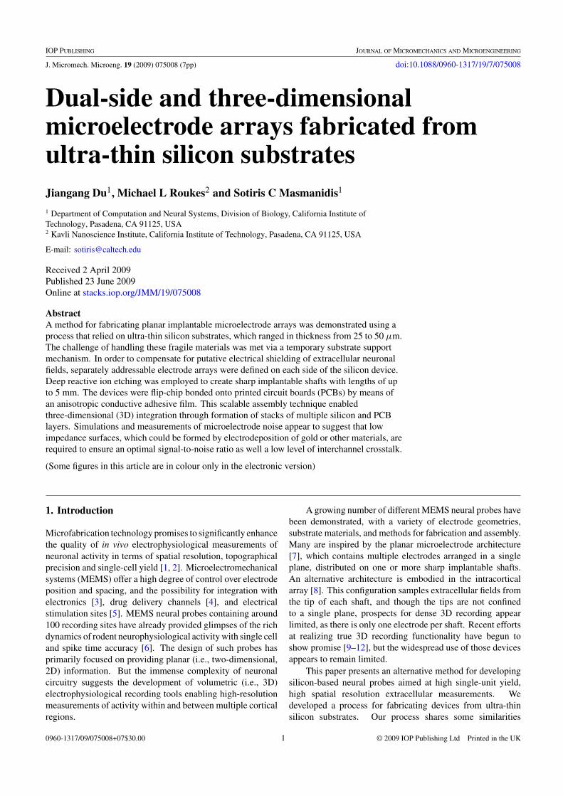
In order to avoid fracturing the device wafers, a supportingcarrier substrate is used for all critical fabrication steps. Thecarrier is typically comprised of 500 μm thick Si, Pyrex orquartz. For a majority of processing steps the ultra-thin waferis temporarily bonded to the carrier by means of a polymericadhesive (WaferGrip, Dynatex), and debonded by means of ahot solvent (StripAid, Dynatex). The polymeric adhesive isplaced between the carrier substrate and the device substrate.In the event of asymmetric stress between the two sides of thedevice wafer, a small weight is added on top to ensure uniformcontact. The stack is then placed in a room-temperaturevacuum oven that is allowed to reach 110 ◦C for 30 min, andthen cooled back to room temperature, after which it is readyfor processing. The long thermal cycling time ensures theultra-thin wafer is uniformly adhered to the carrier, which isessential for enabling the subsequent photolithography steps.
Figure 1. Fabrication process flow for single-side neural probearray built from ultra-thin silicon substrates. Each step relies on theuse of a rigid supporting wafer to maintain structural integrity of thedevice substrate.
In the final DRIE step, the adhesive is replaced with athin layer of spun-on photoresist (AZ-9245, AZ ElectronicMaterials), which appears to provide better thermal anchoringto the carrier substrate. After the stack has been made, it isbaked at 110 ◦C for 60 min.
2.2. The single-side device process
The neural recording arrays are manufactured using a seriesof surface- and bulk-micromachining processing steps, whichare illustrated in figure 1. Our single-side devices onlycontain recording sites on the front side of the wafer, andwhile these are not as functionally powerful as dual-sidearrays, they serve as a useful starting point for describingour fabrication process. We use a double-side polished50 mm diameter Si (1 0 0) substrate with thickness rangingfrom 25 to 50 ± 5 μm (Virginia Semiconductor). Thesubstrates are first thermally oxidized to yield a 2 μm oxidelayer on both sides. Next, a negative tone photoresist (nLOF-2035, AZ Electronic Materials) is spun on and patterned todefine the metal layer comprising the recording electrodes,interconnects and flip-chip contact pads. Metallizationconsists of a 30 A Cr adhesion layer followed by 1500 AAu. After lifting off the unpatterned metal and photoresist,the wafer is flipped over, remounted on a temporary carrier,and the oxide is selectively removed from the backside usinga photoresist mask. This step is vital to obtaining stress-balanced shafts. The wafer is flipped over again to its originalorientation, and an RIE step is applied to remove the oxidelayer from the front side, forming the shaft profile. A 2 ± 1 μmparylene C film is then conformally deposited and patternedwith an oxygen plasma [19], at which point the insulationlayers are fully defined, and the Au recording sites are exposed.For the final DRIE step, a 20 μm thick photoresist film (AZ-9260, AZ Electronic Materials) serves as the masking layer.
2
J. Micromech. Microeng. 19 (2009) 075008 J Du et al
(a)
(b)
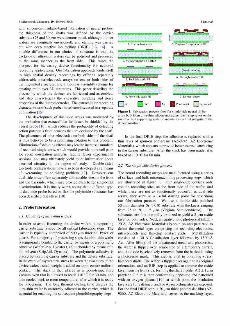
Figure 2. (a) Structure of a typical neural probe. This devicecontains two 5 mm long shafts. The inset shows the recordingelectrode arrangement. (b) SEM image of the tip of a fabricatedprobe. The gold electrodes have an area of 100 μm2, and the shaftshave a thickness of 50 μm.
After the etch, the probes are rinsed in acetone, isopropanoland ethanol to remove the photoresist and DRIE residues.
A representative fabricated device is shown in figure 2(a),with an expanded SEM view of the tip in figure 2(b). Thisparticular array employs 16 recording sites distributed on 2shafts, which have dimensions of 5 mm × 90 μm × 50 μm(l × w × t), and a horizontal tip spacing of 190 μm. Therecording sites have an area of 10 × 10 μm2, and are 30 μmapart. Interconnecting wires have a width and separation of2 μm. As with other planar MEMS neural probes, the arraydesign can be tailored into a plethora of configurations.
2.3. Process modification for dual-side devices
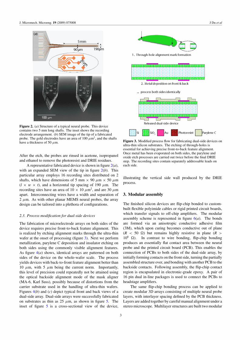
The fabrication of microelectrode arrays on both sides of thedevice requires precise front-to-back feature alignment. Thisis realized by etching alignment marks through the ultra-thinwafer at the onset of processing (figure 3). Next we performmetallization, parylene C deposition and insulator etching onboth sides using the commonly visible alignment features.As figure 4(a) shows, identical arrays are patterned on bothsides of the device on the whole-wafer scale. The processyields devices with back-to-front feature alignment better than10 μm, with 5 μm being the current norm. Importantly,this level of precision could repeatedly not be attained usingthe optical backside alignment mode of the mask aligner(MA-6, Karl Suss), possibly because of distortions from thecarrier substrate used in the handling of ultra-thin wafers.Figures 4(b) and (c) depict typical front and back views of adual-side array. Dual-side arrays were successfully fabricatedon substrates as thin as 25 μm, as shown in figure 5. Theinset of figure 5 is a cross-sectional view of the device,
Figure 3. Modified process flow for fabricating dual-side devices onultra-thin silicon substrates. The etching of through-holes isessential for achieving precise front-to-back feature alignment.Once metal has been evaporated on both sides, the parylene andoxide etch processes are carried out twice before the final DRIEstep. The recording sites contain separately addressable leads oneach side.
illustrating the vertical side wall produced by the DRIEprocess.
3. Modular assembly
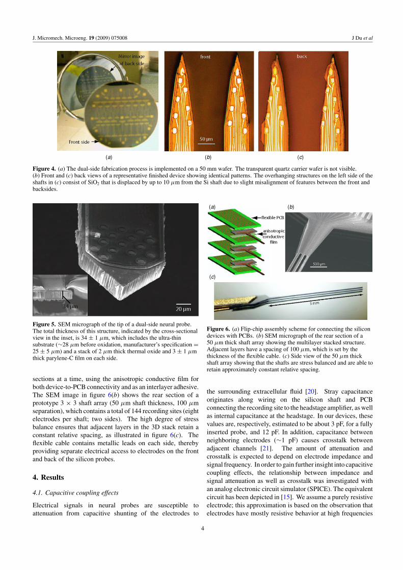
The finished silicon devices are flip-chip bonded to custom-built flexible polyimide cables or rigid printed circuit boards,which transfer signals to off-chip amplifiers. The modularassembly scheme is represented in figure 6(a). The bondsare formed via an anisotropic conductive adhesive film(3M), which upon curing becomes conductive out of plane(R < 50 �) but remains highly resistive in plane (R >
108 �). In contrast to wire bonding, flip-chip bondingproduces an essentially flat contact area between the neuralprobe and the printed circuit board (PCB). This enables theconnection of PCBs to both sides of the dual-side array, byinitially forming contacts on the front side, turning the partiallyassembled structure over, and bonding with another PCB to thebackside contacts. Following assembly, the flip-chip contactregion is encapsulated in electronic-grade epoxy. A pair of16 pin dual in-line packages is used to connect the PCBs toheadstage amplifiers.
The same flip-chip bonding process can be applied tocreate modular 3D arrays consisting of multiple neural probelayers, with interlayer spacing defined by the PCB thickness.Layers are added together by careful manual alignment under astereo microscope. Multilayer structures are built two modular
3
J. Micromech. Microeng. 19 (2009) 075008 J Du et al
(a) (b) (c)
Figure 4. (a) The dual-side fabrication process is implemented on a 50 mm wafer. The transparent quartz carrier wafer is not visible.(b) Front and (c) back views of a representative finished device showing identical patterns. The overhanging structures on the left side of theshafts in (c) consist of SiO2 that is displaced by up to 10 μm from the Si shaft due to slight misalignment of features between the front andbacksides.
Figure 5. SEM micrograph of the tip of a dual-side neural probe.The total thickness of this structure, indicated by the cross-sectionalview in the inset, is 34 ± 1 μm, which includes the ultra-thinsubstrate (∼28 μm before oxidation, manufacturer’s specification =25 ± 5 μm) and a stack of 2 μm thick thermal oxide and 3 ± 1 μmthick parylene-C film on each side.
sections at a time, using the anisotropic conductive film forboth device-to-PCB connectivity and as an interlayer adhesive.The SEM image in figure 6(b) shows the rear section of aprototype 3 × 3 shaft array (50 μm shaft thickness, 100 μmseparation), which contains a total of 144 recording sites (eightelectrodes per shaft; two sides). The high degree of stressbalance ensures that adjacent layers in the 3D stack retain aconstant relative spacing, as illustrated in figure 6(c). Theflexible cable contains metallic leads on each side, therebyproviding separate electrical access to electrodes on the frontand back of the silicon probes.
4. Results
4.1. Capacitive coupling effects
Electrical signals in neural probes are susceptible toattenuation from capacitive shunting of the electrodes to
(a) (b)
(c)
Figure 6. (a) Flip-chip assembly scheme for connecting the silicondevices with PCBs. (b) SEM micrograph of the rear section of a50 μm thick shaft array showing the multilayer stacked structure.Adjacent layers have a spacing of 100 μm, which is set by thethickness of the flexible cable. (c) Side view of the 50 μm thickshaft array showing that the shafts are stress balanced and are able toretain approximately constant relative spacing.
the surrounding extracellular fluid [20]. Stray capacitanceoriginates along wiring on the silicon shaft and PCBconnecting the recording site to the headstage amplifier, as wellas internal capacitance at the headstage. In our devices, thesevalues are, respectively, estimated to be about 3 pF, for a fullyinserted probe, and 12 pF. In addition, capacitance betweenneighboring electrodes (∼1 pF) causes crosstalk betweenadjacent channels [21]. The amount of attenuation andcrosstalk is expected to depend on electrode impedance andsignal frequency. In order to gain further insight into capacitivecoupling effects, the relationship between impedance andsignal attenuation as well as crosstalk was investigated withan analog electronic circuit simulator (SPICE). The equivalentcircuit has been depicted in [15]. We assume a purely resistiveelectrode; this approximation is based on the observation thatelectrodes have mostly resistive behavior at high frequencies
4
J. Micromech. Microeng. 19 (2009) 075008 J Du et al
(a) (b)
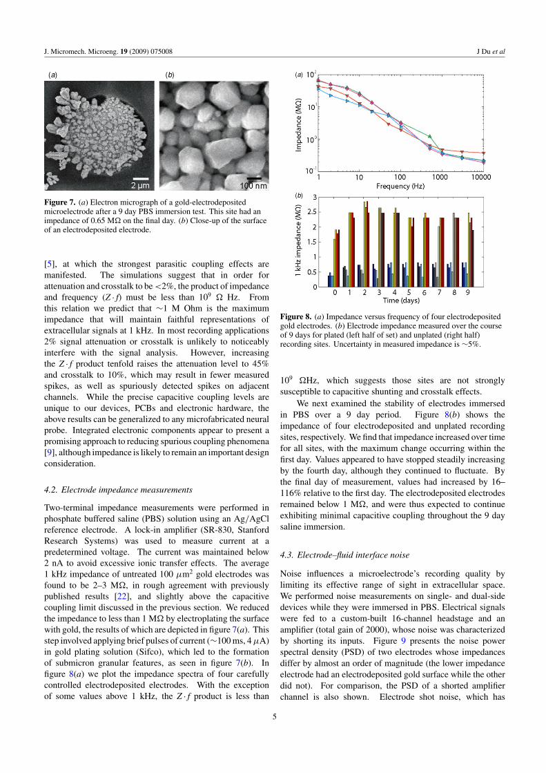
Figure 7. (a) Electron micrograph of a gold-electrodepositedmicroelectrode after a 9 day PBS immersion test. This site had animpedance of 0.65 M� on the final day. (b) Close-up of the surfaceof an electrodeposited electrode.
[5], at which the strongest parasitic coupling effects aremanifested. The simulations suggest that in order forattenuation and crosstalk to be <2%, the product of impedanceand frequency (Z · f) must be less than 109 � Hz. Fromthis relation we predict that ∼1 M Ohm is the maximumimpedance that will maintain faithful representations ofextracellular signals at 1 kHz. In most recording applications2% signal attenuation or crosstalk is unlikely to noticeablyinterfere with the signal analysis. However, increasingthe Z · f product tenfold raises the attenuation level to 45%and crosstalk to 10%, which may result in fewer measuredspikes, as well as spuriously detected spikes on adjacentchannels. While the precise capacitive coupling levels areunique to our devices, PCBs and electronic hardware, theabove results can be generalized to any microfabricated neuralprobe. Integrated electronic components appear to present apromising approach to reducing spurious coupling phenomena[9], although impedance is likely to remain an important designconsideration.
4.2. Electrode impedance measurements
Two-terminal impedance measurements were performed inphosphate buffered saline (PBS) solution using an Ag/AgClreference electrode. A lock-in amplifier (SR-830, StanfordResearch Systems) was used to measure current at apredetermined voltage. The current was maintained below2 nA to avoid excessive ionic transfer effects. The average1 kHz impedance of untreated 100 μm2 gold electrodes wasfound to be 2–3 M�, in rough agreement with previouslypublished results [22], and slightly above the capacitivecoupling limit discussed in the previous section. We reducedthe impedance to less than 1 M� by electroplating the surfacewith gold, the results of which are depicted in figure 7(a). Thisstep involved applying brief pulses of current (∼100 ms, 4 μA)in gold plating solution (Sifco), which led to the formationof submicron granular features, as seen in figure 7(b). Infigure 8(a) we plot the impedance spectra of four carefullycontrolled electrodeposited electrodes. With the exceptionof some values above 1 kHz, the Z · f product is less than
(a)
(b)
Figure 8. (a) Impedance versus frequency of four electrodepositedgold electrodes. (b) Electrode impedance measured over the courseof 9 days for plated (left half of set) and unplated (right half)recording sites. Uncertainty in measured impedance is ∼5%.
109 �Hz, which suggests those sites are not stronglysusceptible to capacitive shunting and crosstalk effects.
We next examined the stability of electrodes immersedin PBS over a 9 day period. Figure 8(b) shows theimpedance of four electrodeposited and unplated recordingsites, respectively. We find that impedance increased over timefor all sites, with the maximum change occurring within thefirst day. Values appeared to have stopped steadily increasingby the fourth day, although they continued to fluctuate. Bythe final day of measurement, values had increased by 16–116% relative to the first day. The electrodeposited electrodesremained below 1 M�, and were thus expected to continueexhibiting minimal capacitive coupling throughout the 9 daysaline immersion.
4.3. Electrode–fluid interface noise
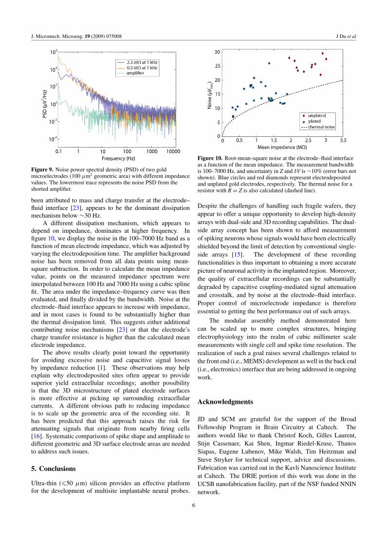
Noise influences a microelectrode’s recording quality bylimiting its effective range of sight in extracellular space.We performed noise measurements on single- and dual-sidedevices while they were immersed in PBS. Electrical signalswere fed to a custom-built 16-channel headstage and anamplifier (total gain of 2000), whose noise was characterizedby shorting its inputs. Figure 9 presents the noise powerspectral density (PSD) of two electrodes whose impedancesdiffer by almost an order of magnitude (the lower impedanceelectrode had an electrodeposited gold surface while the otherdid not). For comparison, the PSD of a shorted amplifierchannel is also shown. Electrode shot noise, which has
5
J. Micromech. Microeng. 19 (2009) 075008 J Du et al
Figure 9. Noise power spectral density (PSD) of two goldmicroelectrodes (100 μm2 geometric area) with different impedancevalues. The lowermost trace represents the noise PSD from theshorted amplifier.
been attributed to mass and charge transfer at the electrode–fluid interface [23], appears to be the dominant dissipationmechanism below ∼30 Hz.
A different dissipation mechanism, which appears todepend on impedance, dominates at higher frequency. Infigure 10, we display the noise in the 100–7000 Hz band as afunction of mean electrode impedance, which was adjusted byvarying the electrodeposition time. The amplifier backgroundnoise has been removed from all data points using mean-square subtraction. In order to calculate the mean impedancevalue, points on the measured impedance spectrum wereinterpolated between 100 Hz and 7000 Hz using a cubic splinefit. The area under the impedance–frequency curve was thenevaluated, and finally divided by the bandwidth. Noise at theelectrode–fluid interface appears to increase with impedance,and in most cases is found to be substantially higher thanthe thermal dissipation limit. This suggests either additionalcontributing noise mechanisms [23] or that the electrode’scharge transfer resistance is higher than the calculated meanelectrode impedance.
The above results clearly point toward the opportunityfor avoiding excessive noise and capacitive signal lossesby impedance reduction [1]. These observations may helpexplain why electrodeposited sites often appear to providesuperior yield extracellular recordings; another possibilityis that the 3D microstructure of plated electrode surfacesis more effective at picking up surrounding extracellularcurrents. A different obvious path to reducing impedanceis to scale up the geometric area of the recording site. Ithas been predicted that this approach raises the risk forattenuating signals that originate from nearby firing cells[16]. Systematic comparisons of spike shape and amplitude todifferent geometric and 3D surface electrode areas are neededto address such issues.
5. Conclusions
Ultra-thin (�50 μm) silicon provides an effective platformfor the development of multisite implantable neural probes.
Figure 10. Root-mean-square noise at the electrode–fluid interfaceas a function of the mean impedance. The measurement bandwidthis 100–7000 Hz, and uncertainty in Z and δV is ∼10% (error bars notshown). Blue circles and red diamonds represent electrodepositedand unplated gold electrodes, respectively. The thermal noise for aresistor with R = Z is also calculated (dashed line).
Despite the challenges of handling such fragile wafers, theyappear to offer a unique opportunity to develop high-densityarrays with dual-side and 3D recording capabilities. The dual-side array concept has been shown to afford measurementof spiking neurons whose signals would have been electricallyshielded beyond the limit of detection by conventional single-side arrays [15]. The development of these recordingfunctionalities is thus important to obtaining a more accuratepicture of neuronal activity in the implanted region. Moreover,the quality of extracellular recordings can be substantiallydegraded by capacitive coupling-mediated signal attenuationand crosstalk, and by noise at the electrode–fluid interface.Proper control of microelectrode impedance is thereforeessential to getting the best performance out of such arrays.
The modular assembly method demonstrated herecan be scaled up to more complex structures, bringingelectrophysiology into the realm of cubic millimeter scalemeasurements with single cell and spike time resolution. Therealization of such a goal raises several challenges related tothe front end (i.e., MEMS) development as well in the back end(i.e., electronics) interface that are being addressed in ongoingwork.
Acknowledgments
JD and SCM are grateful for the support of the BroadFellowship Program in Brain Circuitry at Caltech. Theauthors would like to thank Christof Koch, Gilles Laurent,Stijn Cassenaer, Kai Shen, Ingmar Riedel-Kruse, ThanosSiapas, Eugene Lubenov, Mike Walsh, Tim Heitzman andSteve Stryker for technical support, advice and discussions.Fabrication was carried out in the Kavli Nanoscience Instituteat Caltech. The DRIE portion of this work was done in theUCSB nanofabrication facility, part of the NSF funded NNINnetwork.
6

J. Micromech. Microeng. 19 (2009) 075008 J Du et al
References
[1] Cheung K 2007 Implantable microscale neural interfacesBiomed. Microdevices 9 923–38
[2] Wise K D, Sodagar A M, Yao Y, Ning Gulari M, Perlin G Eand Najafi K 2008 Microelectrodes, microelectronics, andimplantable neural microsystems Proc. IEEE96 1184–202
[3] Najafi K and Wise K D 1986 An implantable multielectrodearray with on-chip signal processing IEEE J. Solid-StateCircuits 21 1035–44
[4] Chen J, Wise K D, Hetke J F and Bledsoe S C 1997 Amultichannel neural probe for selective chemicaldelivery at the cellular level IEEE Trans. Biomed. Eng.44 760–9
[5] Anderson D J, Najafi K, Tanghe S J, Evans D A, Levy K L,Hetke J F, Xue X, Zappia J J and Wise K D 1989Batch-fabricated thin-film electrodes for stimulation of thecentral auditory system IEEE Trans. Biomed. Eng.36 693–704
[6] Csicsvari J, Henze D A, Jamieson B, Harris K D, Sirota A,Bartho P, Wise K D and Buzsaki G 2003 Massivelyparallel recording of unit and local field potentialswith silicon-based electrodes J. Neurophysiol.90 1314–23
[7] Najafi K, Wise K D and Mochizuki T 1985 A high-yieldIC-compatible multichannel recording array IEEE Trans.Electron Devices 32 1206–11
[8] Campbell P K, Jones K E, Huber R J, Horch K Wand Normann R A 1991 A silicon-based, three dimensionalneural interface: manufacturing processes for anintracortical electrode array IEEE Trans. Biomed. Eng.38 758–68
[9] Bai Q, Wise K D and Anderson D J 2000 A high-yieldmicroassembly structure for three-dimensionalmicroelectrode arrays IEEE Trans. Biomed. Eng.47 281–9
[10] Yao Y, Ning Gulari M, Wiler J A and Wise K D 2007 Amicroassembled low-profile three-dimensionalmicroelectrode array for neural prosthesis applicationsJ. Microelectromech. Syst. 16 977–88
[11] Takeuchi S, Suzuki T, Mabuchi K and Fujita H 2004 3Dflexible multichannel neural probe array J. Micromech.Microeng. 14 104–7
[12] Neves H P, Orban G A, Koudelka-Hep M, Stieglitz Tand Ruther P 2007 Development of modularmultifunctional probe arrays for cerebral applications Proc.IEEE Eng. Med. Biol. Soc. 104–9
[13] Norlin P, Kindlundh M, Mouroux A, Yoshida K andHofmann U G 2002 A 32-site neural recording probefabricated by DRIE of SOI substrates J. Micromech.Microeng. 12 414–9
[14] Cheung K C, Djupsund K, Dan Y and Lee L P 2003Implantable multichannel electrode array based on SOItechnology J. Microelectromech. Syst 12 179–84
[15] Du J, Riedel-Kruse I H, Nawroth J C, Roukes M L, Laurent Gand Masmanidis S C 2009 High-resolutionthree-dimensional extracellular recording of neuronalactivity with microfabricated electrode arrays J.Neurophysiol. 101 1671–8
[16] Moffitt M A and McIntyre C C 2005 Model-based analysis ofcortical recording with silicon microelectrodes Clin.Neurophysiol. 116 2240–50
[17] Perlin G E and Wise K D 2004 The effect of the substrate onthe extracellular neural activity recorded withmicromachined silicon microprobes Conf. Proc. IEEE Eng.Med. Biol. Soc. 2002–5
[18] Stieglitz T and Gross M 2002 Flexible BIOMEMS withelectrode arrangements on front and back side as keycomponent in neural prostheses and biohybrid systemsSensors Actuators B 83 8–14
[19] Pang C, Cham J G, Nenadic Z, Musallam S, Tai Y C,Burdick J W and Andersen R A 2005 A new multi-siteprobe array with monolithically integrated parylene flexiblecable for neural prostheses Conf. Proc. IEEE Eng. Med.Biol. Soc. p 7114
[20] Robinson D A 1968 The electrical properties of metalmicroelectrodes Proc. IEEE 56 1065–71
[21] Najafi K, Ji J and Wise K D 1990 Scaling limitations of siliconmicromachined recording probes IEEE Trans. Biomed. Eng.37 1–11
[22] Drake K L, Wise K D, Farraye J, Anderson D J andBeMent S L 1988 Performance of planar multisitemicroprobes in recording extracellular single-unitintracortical activity IEEE Trans. Biomed. Eng. 35 719–32
[23] Hassibi A, Navid R, Dutton R W and Lee T H 2004Comprehensive study of noise processes in electrodeelectrolyte interfaces J. Appl. Phys. 96 1074–82
7


![ViX Series - Micromech · in the global industrial market. ... advanced operations such as external encoder following and registration ... Capacitance power module [µF] 3300 6600](https://static.fdocuments.in/doc/165x107/5b08adb97f8b9a3d018c8891/vix-series-the-global-industrial-market-advanced-operations-such-as-external.jpg)

