Hong Young Chang - SEMATECH 5-450... · Hong Young Chang Department of Physics, Korea Advanced...
41
Hong Young Chang Department of Physics, Korea Advanced Institute of Science and Technology (KAIST), Republic of Korea
Transcript of Hong Young Chang - SEMATECH 5-450... · Hong Young Chang Department of Physics, Korea Advanced...
Hong Young ChangDepartment of Physics, Korea Advanced Institute of Science
and Technology (KAIST), Republic of Korea

1. Introduction
2. Some plasma sources
3. Related issues
4. Summary
Index
-2

Why is Large Area Plasma Source important?
• Process glass size increases continuously. (8 G : 2200 mm X 2500 mm)
Flat Panel Display
• Microcrystalline Si deposition using Large Area Very High Frequency(VHF) plasma
Si thin film Solar Cell
• Dual Frequency CCP (using VHF), wafer size increases continuously.
• Near future, 450 mm wafer will be used.
Semiconductor
-3
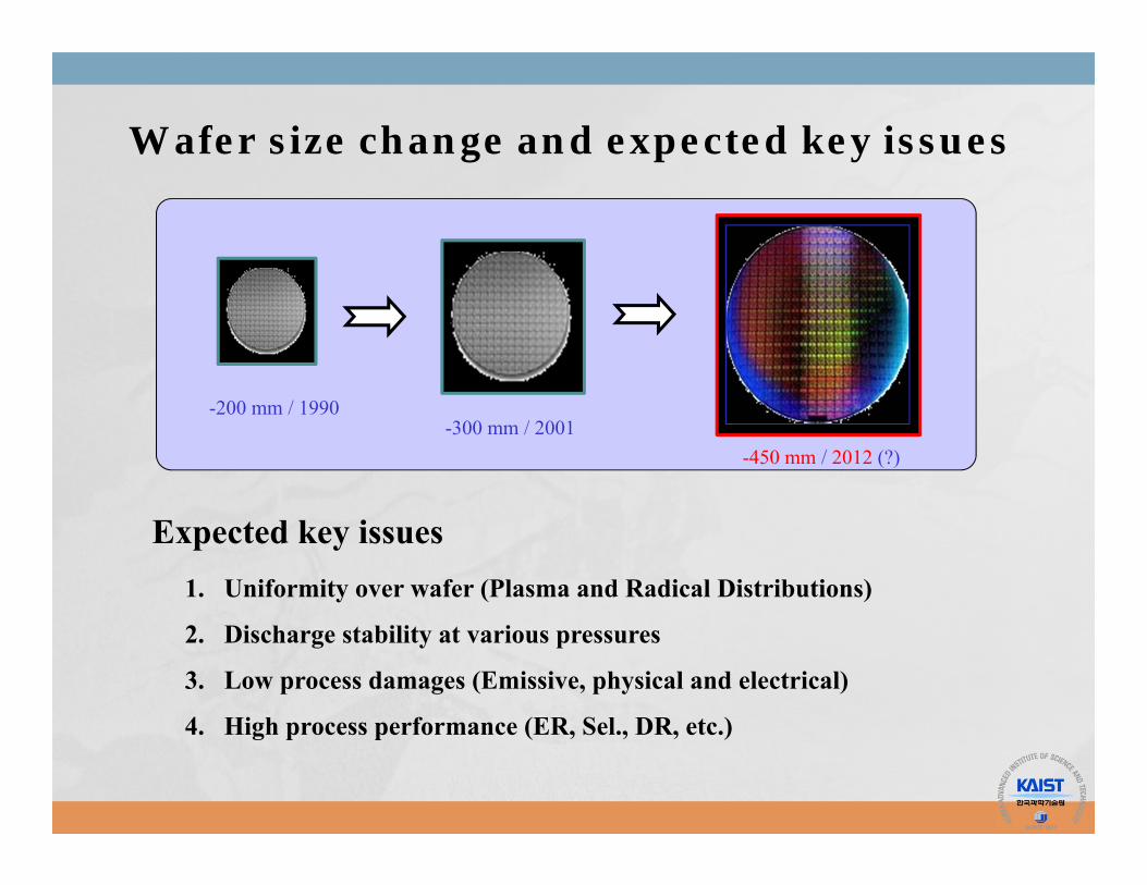
1. Uniformity over wafer (Plasma and Radical Distributions)
2. Discharge stability at various pressures
3. Low process damages (Emissive, physical and electrical)
4. High process performance (ER, Sel., DR, etc.)
-200 mm / 1990-300 mm / 2001
-450 mm / 2012 (?)
Wafer size change and expected key issues
Expected key issues

Plasma frequency dependence of electron density and electron temperature -argon plasmapower density: 0.13 W/cm2, pressure : 50 & 20 mTorr. M. Takai et al. J. Non-Cryst. Solids 266-269 (2000) 90
Why is VHF Plasma needed?
Driving frequency ↑
↑eP
iP ↓ Ion bombardment energy ↓
Electron density ↑
Electron temperature ↓
PIC calculation, at 2.67 Pa
S. J. You, et al. J. Appl. Phys. vol. 94 no. 12 7422
-5
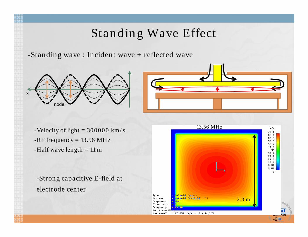
Standing Wave Effect
-Standing wave : Incident wave + reflected wave
-Velocity of light = 300000 km/s
-RF frequency = 13.56 MHz
-Half wave length = 11 m
node
x
2.3 m
13.56 MHz
-Strong capacitive E-field at
electrode center
-6
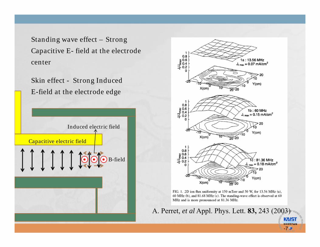
B-field
Capacitive electric field
Induced electric field
Skin effect - Strong Induced
E-field at the electrode edge
A. Perret, et al Appl. Phys. Lett. 83, 243 (2003)
Standing wave effect – Strong
Capacitive E- field at the electrode
center
-7
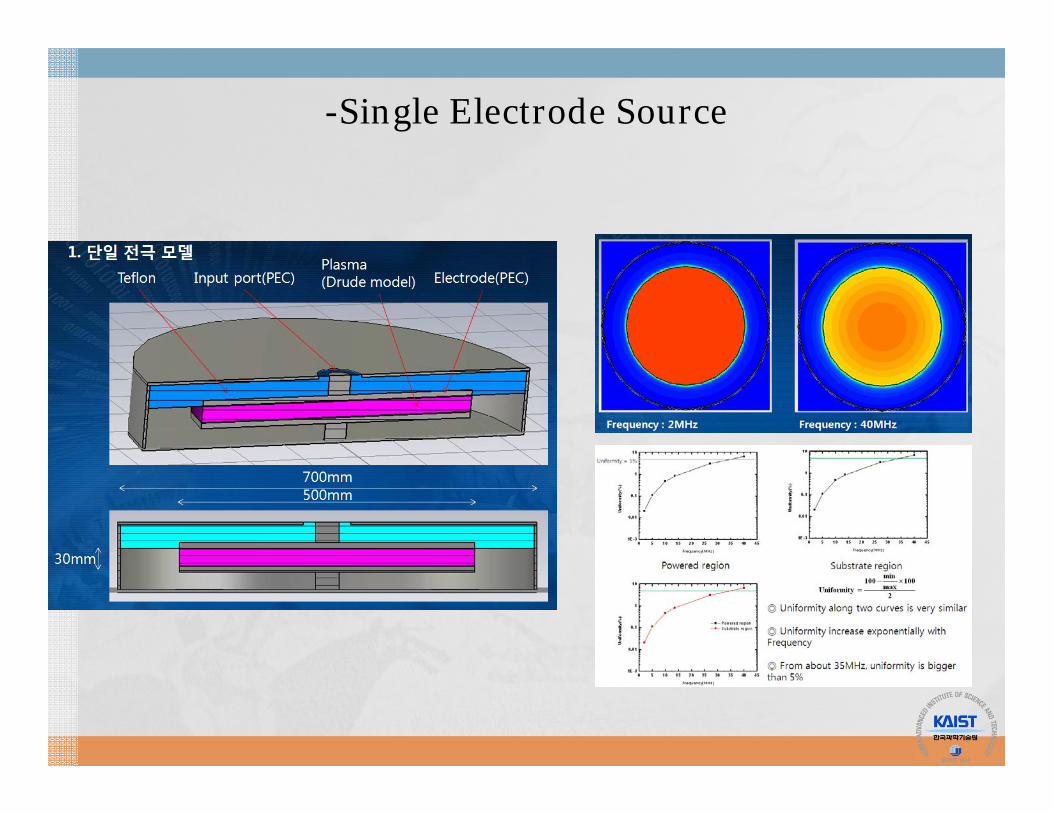
-Single Electrode Source

Multi-feeding source
-View of multi feeding port
-Simulation result
0 100 200 300 400 5000
500
1,000
1,500
E-fie
ld (A
.U)
Length
13.56 MHz 27.12 MHz 40 MHz
10 15 20 25 30 35 40 45
1
10
single feeding multi feeding
Non
-Uni
form
ity(%
)
Frequency(MHz)
-There is little uniformity difference between single feeding and multi feeding
concept.
-Another concept is needed.
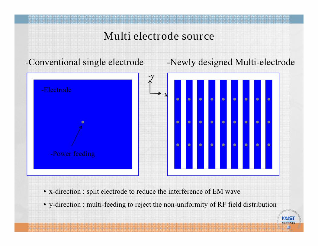
-Power feeding
-Electrode
-Conventional single electrode -Newly designed Multi-electrode
-x
-y
• x-direction : split electrode to reduce the interference of EM wave
• y-direction : multi-feeding to reject the non-uniformity of RF field distribution
Multi electrode source
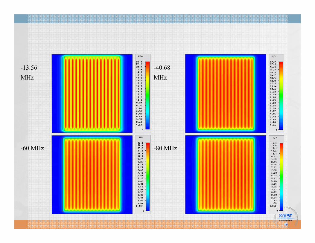
-13.56 MHz
-40.68 MHz
-60 MHz -80 MHz

-Diagnostic results – Plasma uniformity
-20-10
010
20
0.4
0.5
0.6
0.7
0.8
0.9
1.0
-20
-10
010
20
J i/Ji m
ax
Y (cm)
X (cm)
-10.3% -20-10
010
20
0.4
0.5
0.6
0.7
0.8
0.9
1.0
-20
-10
010
20
J i/Ji m
ax
Y (cm)
X (cm)
-12.6%
-< Example of measured result with probe array in Normal CCP>
-< 8x8 Probe array>
• Measured the spatial profile of the ion saturation current with the homemade probe array

Multi electrode source
- Multi electrode
- 13.56 MHz - 40 MHz-13
2
100maxmin100
uniformity-Non
- Non-uniformity-4.03%
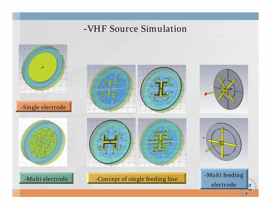
-VHF Source Simulation
-14
-Single electrode
-Multi electrode -Concept of single feeding line-Multi feeding
electrode

-VHF Source Installation
-450mm plasma equipment
-Installed 450mm CCP sources
-15
-Power input port

-Structure
-Sensor Arrays-- SiO2 coated PCB
-Al2O3 anodized-Shielding case
-Data cable-diameter(<23mm)
-Vacuum feedthrough-- NW25
-2D probe
-Ground-Electrode
-2D Probe
- ~ 500 mm
-ID 700 mm
-Powered electrode
-Vacuum port (NW25)-&
-Vacuum feedthrough-Data cable
-450 mm
-Chamber
-buttress
-2D Probe Array Installation
-17
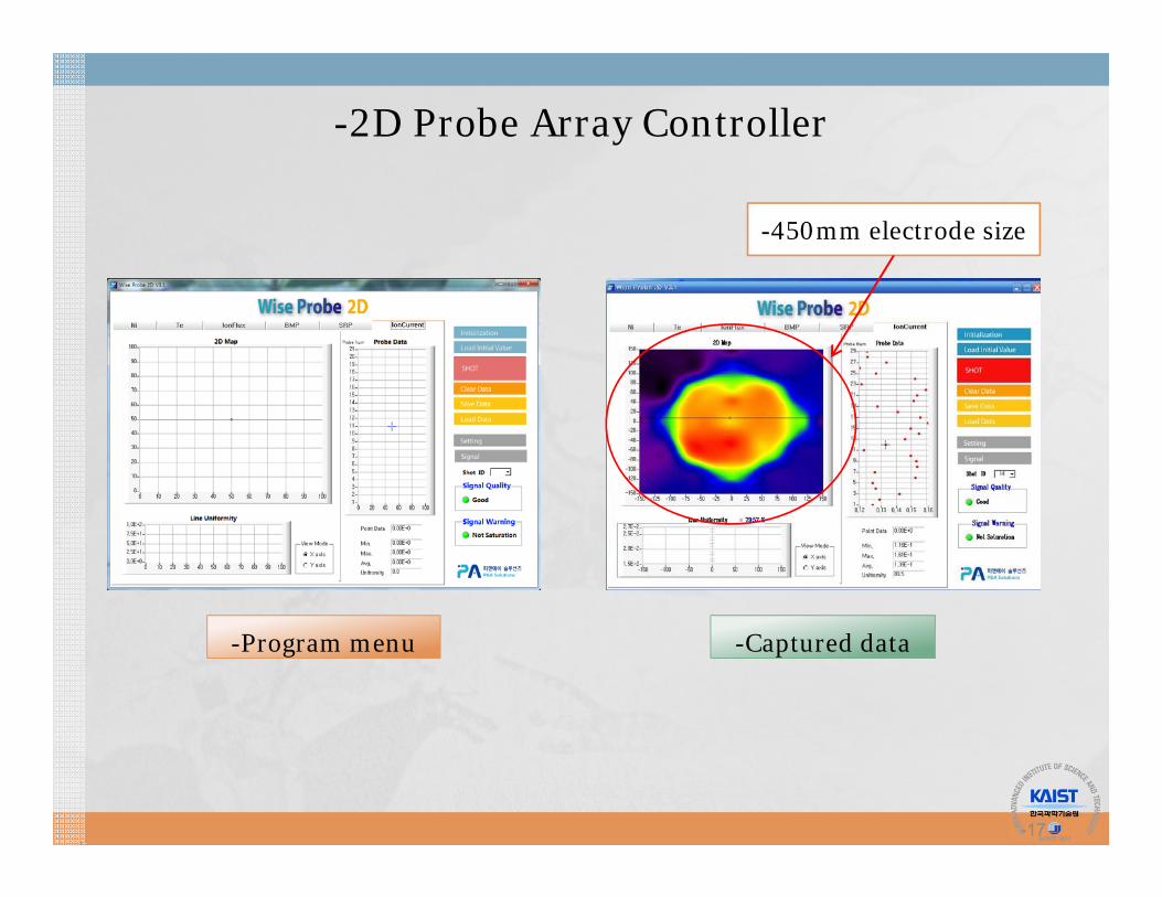
-2D Probe Array Controller
-Program menu -Captured data
-450mm electrode size
-18
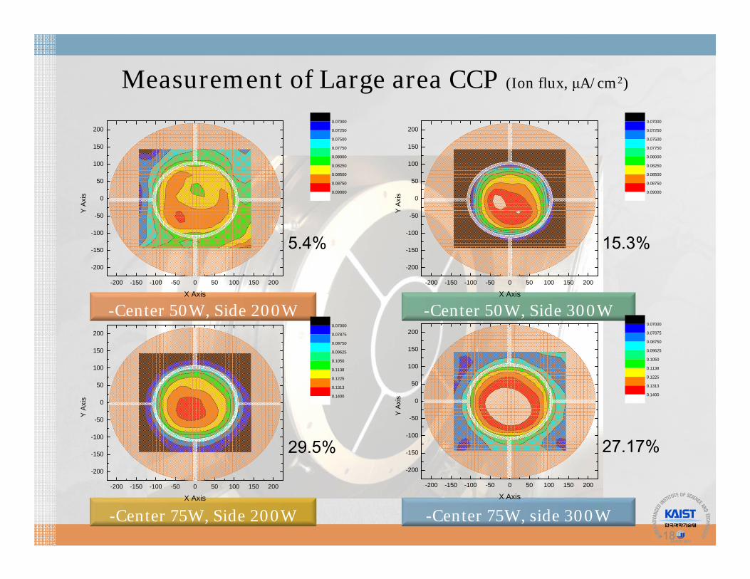
-Center 50W, Side 200W -Center 50W, Side 300W
-Center 75W, Side 200W -Center 75W, side 300W
Measurement of Large area CCP (Ion flux, μA/cm2)
-200 -150 -100 -50 0 50 100 150 200
-200
-150
-100
-50
0
50
100
150
200
X Axis
Y A
xis
0.07000
0.07250
0.07500
0.07750
0.08000
0.08250
0.08500
0.08750
0.09000
-200 -150 -100 -50 0 50 100 150 200
-200
-150
-100
-50
0
50
100
150
200
X Axis
Y A
xis
0.07000
0.07250
0.07500
0.07750
0.08000
0.08250
0.08500
0.08750
0.09000
-200 -150 -100 -50 0 50 100 150 200
-200
-150
-100
-50
0
50
100
150
200
X Axis
Y Ax
is
0.07000
0.07875
0.08750
0.09625
0.1050
0.1138
0.1225
0.1313
0.1400
-200 -150 -100 -50 0 50 100 150 200
-200
-150
-100
-50
0
50
100
150
200
X Axis
Y A
xis
0.07000
0.07875
0.08750
0.09625
0.1050
0.1138
0.1225
0.1313
0.1400
5.4% 15.3%
29.5% 27.17%

-19
-Measurement of Large area CCP (Ion flux, μA/cm2)
9.4% 4.7%
8.3%-200 -150 -100 -50 0 50 100 150 200
-200
-150
-100
-50
0
50
100
150
200
X Axis
Y A
xis
0.030000.036250.042500.048750.055000.061250.067500.073750.080000.086250.092500.098750.10500.11130.11750.12380.1300
-200 -150 -100 -50 0 50 100 150 200
-200
-150
-100
-50
0
50
100
150
200
X Axis
Y A
xis
0.030000.036250.042500.048750.055000.061250.067500.073750.080000.086250.092500.098750.10500.11130.11750.12380.1300
-200 -150 -100 -50 0 50 100 150 200
-200
-150
-100
-50
0
50
100
150
200
X Axis
Y A
xis
0.030000.036250.042500.048750.055000.061250.067500.073750.080000.086250.092500.098750.10500.11130.11750.12380.1300
-Center 50W, Side 125W -Center 125W, Side 125W
-Center 200W, Side 125W

Dual Power Phase Shift Control
Bera K, Rauf S and Collins K 2008 IEEE Trans. Plasma Sci. 36 1366
54 MHz Power Phase Shift of Upper electrode & Lower electrode
-20

Uniformity control by Phase Modulation- Solar cell
K. Kawamura , et al. Thin Solid Films 506-507 (2006) 22-26
-21

Multiple ICP and Helicon Source-Flat Panel Display
• High Density – 1E12 cm-3
• Auto-balancing – equal power absorption
• Low Pressure Operation – about 10 mTorr
Helicon tubes
Permanent Magnet
-22
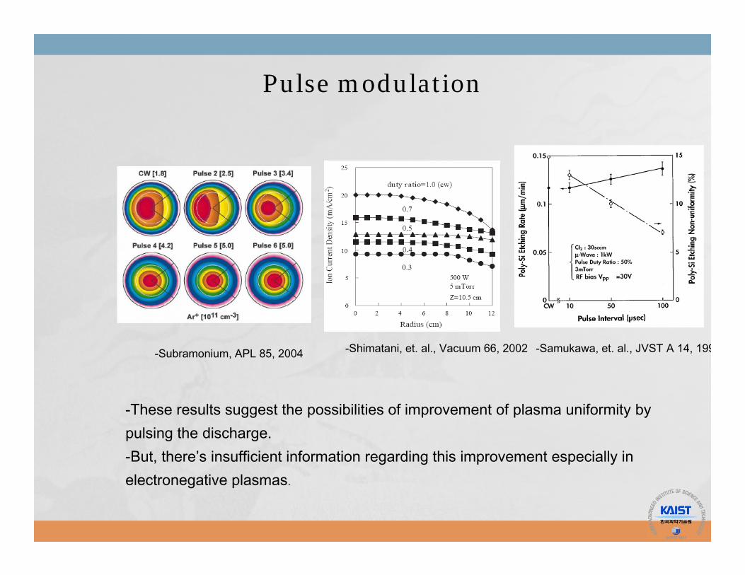
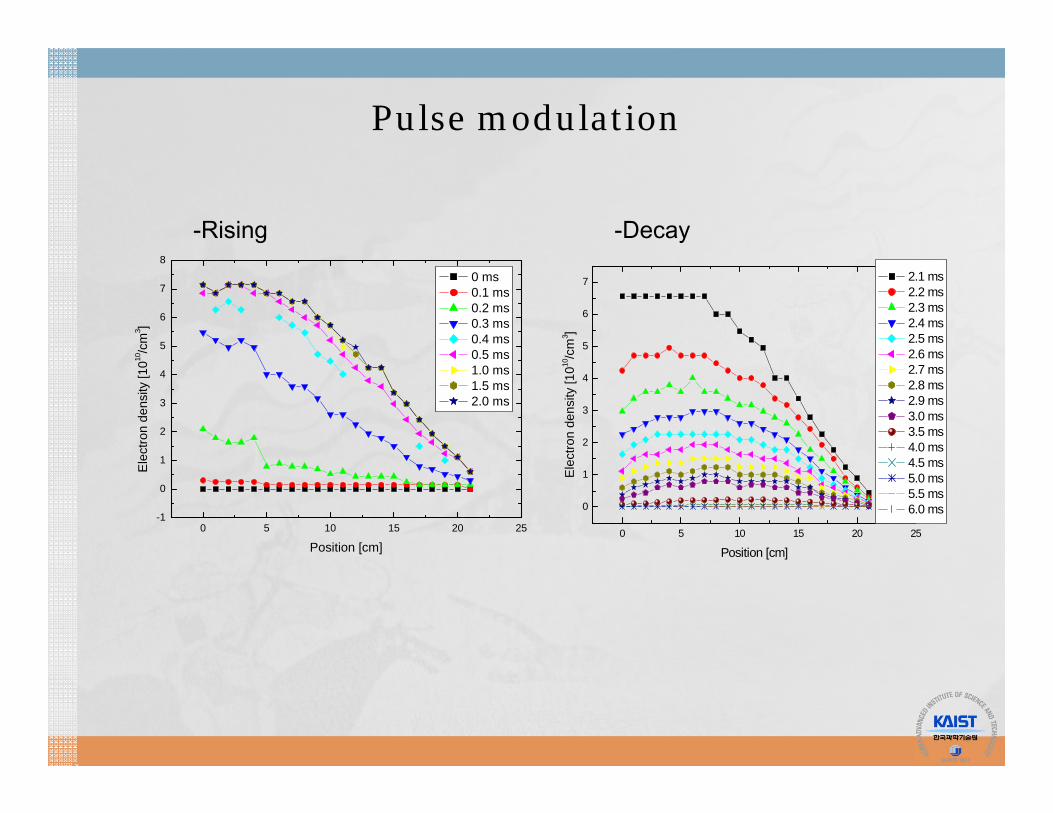
Pulse modulation
-Shimatani, et. al., Vacuum 66, 2002 -Samukawa, et. al., JVST A 14, 199-Subramonium, APL 85, 2004
-These results suggest the possibilities of improvement of plasma uniformity by pulsing the discharge.-But, there’s insufficient information regarding this improvement especially in electronegative plasmas.
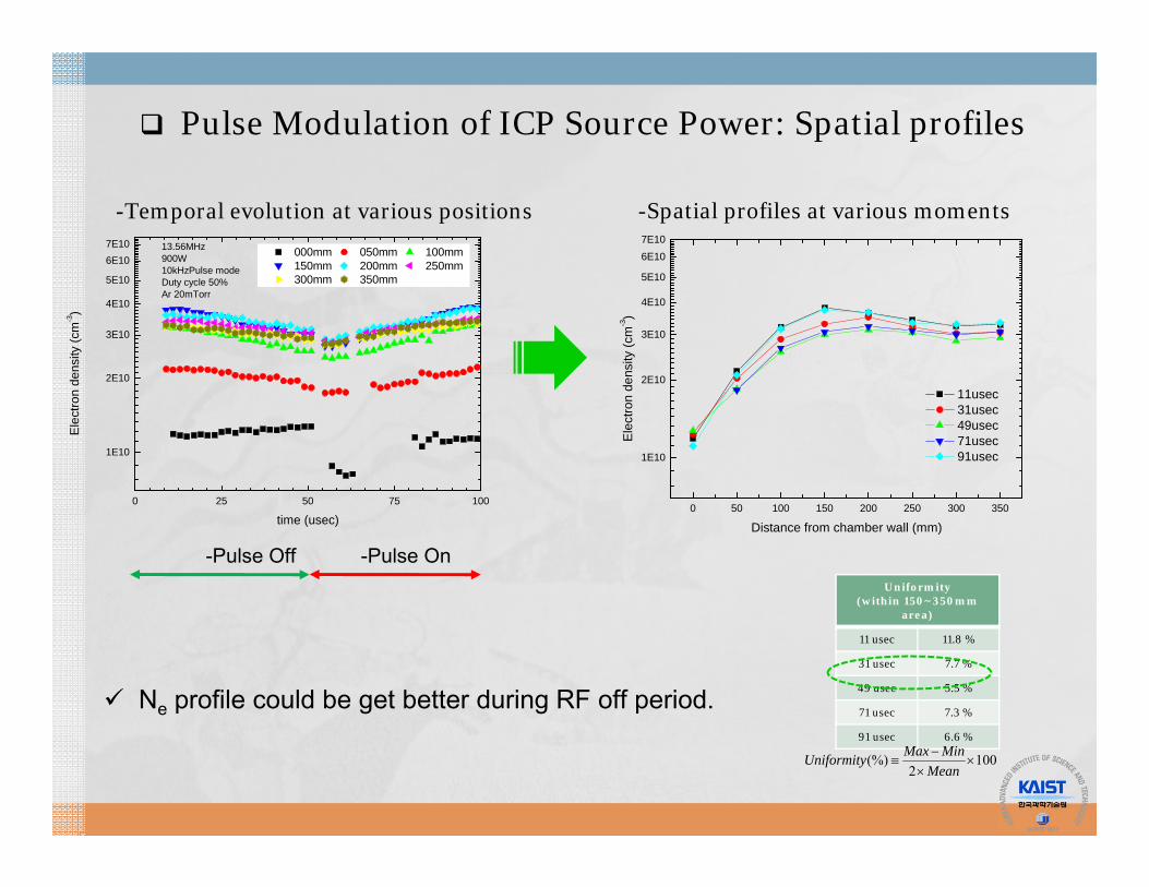
Pulse Modulation of ICP Source Power: Spatial profiles
0 25 50 75 100
1E10
2E10
3E10
4E10
5E10
6E107E10 13.56MHz
900W10kHzPulse modeDuty cycle 50%Ar 20mTorr
000mm 050mm 100mm 150mm 200mm 250mm 300mm 350mm
Ele
ctro
n de
nsity
(cm
-3)
time (usec)0 50 100 150 200 250 300 350
1E10
2E10
3E10
4E10
5E10
6E107E10
11usec 31usec 49usec 71usec 91usec
Elec
tron
dens
ity (c
m-3)
Distance from chamber wall (mm)
Uniformity(within 150~350mm
area)
11 usec 11.8 %
31 usec 7.7 %
49 usec 5.5 %
71 usec 7.3 %
91 usec 6.6 %
1002
(%)
Mean
MinMaxUniformity
-Temporal evolution at various positions -Spatial profiles at various moments
Ne profile could be get better during RF off period.
-Pulse Off -Pulse On
0 5 10 15 20 25
0
1
2
3
4
5
6
7
Ele
ctro
n de
nsity
[1010
/cm
3 ]Position [cm]
2.1 ms 2.2 ms 2.3 ms 2.4 ms 2.5 ms 2.6 ms 2.7 ms 2.8 ms 2.9 ms 3.0 ms 3.5 ms 4.0 ms 4.5 ms 5.0 ms 5.5 ms 6.0 ms
0 5 10 15 20 25-1
0
1
2
3
4
5
6
7
8
Ele
ctro
n de
nsity
[1010
/cm
3 ]
Position [cm]
0 ms 0.1 ms 0.2 ms 0.3 ms 0.4 ms 0.5 ms 1.0 ms 1.5 ms 2.0 ms
-Rising -Decay
Pulse modulation
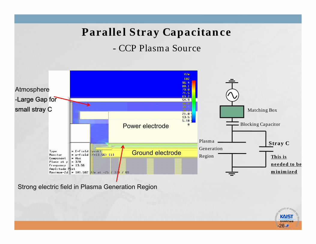
Atmosphere-Large Gap for small stray C
Strong electric field in Plasma Generation Region
Power electrode
Ground electrodeStray C
Blocking Capacitor
Matching Box
This is
needed to be
minimized
Plasma
Generation
Region
Parallel Stray Capacitance- CCP Plasma Source
-26
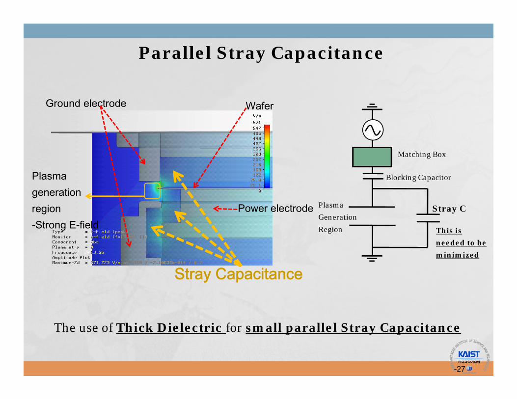
Ground electrode
Power electrode
Wafer
Stray Capacitance
Plasma generation region-Strong E-field
Parallel Stray Capacitance
The use of Thick Dielectric for small parallel Stray Capacitance
Stray C
Blocking Capacitor
Matching Box
This is
needed to be
minimized
Plasma
Generation
Region
-27

Stray Capacitance
Blocking Capacitor
Matching Box
Plasma Generation Region
ground
floating
Plasma
generation
Series Stray Capacitance
Small stray capacitance High voltage is applied Arcing, undesirable discharge
-28

Electromagnetic wave
Surface current
Slot valve
Glass in/out
Slot valve distorts field uniformity as well as
wall surface current flow
Effect of Chamber Wall Asymmetry in CCP
Plasma Source
Ground strap
-29

CCP source’s heating
E
e
Electron in RF electric field
e-n collsion
ne
e
nonlinear sheath interaction
Ohmic Heating
Pressure Heating
Stochastic Heating
collective interaction with sheath
V. A. Godyak
M. M. Turner
• The electron heating in the rf discharges corresponds to how the electrons gain their energy from the rf electric field energy.
Electron heating in the CCP

e
e
Origion of Bi –Maxwellian Electron Distribution
Ramsauer gas effect
Stochastic heating
- Godyak.
Pressure heating
- Turner.
Electron non-local property
- Tsendin, Kaganovich.
sheath sheathe
L
e
EEDF of the CCP
CCP source’s heating

Plasma parameter control with Discharge gap length
60 mTorr, 1A, Gap-changed
elowerf
rf
rfrf
TDEd
dnJE
nEEJ
222/1
2/1/
• The bi-Maxwellian EEPF approaches to the Maxwellian EEPF, because of enhancement of electric field in the bulk with decreasing gap length.
( Gap length ↓ Ne ↓ & Te ↑)
[ S. J. You. et.al , Appl. Phys. Letts, 2005]
CCP source’s heatingCCP source’s heating
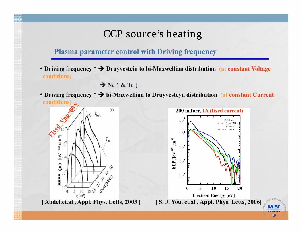
Plasma parameter control with Driving frequency
[ Abdel.et.al , Appl. Phys. Letts, 2003 ]
200 mTorr, 1A (fixed current)
[ S. J. You. et.al , Appl. Phys. Letts, 2006]
• Driving frequency ↑ Druyvestein to bi-Maxwellian distribution (at constant Voltageconditions)
Ne ↑ & Te ↓ • Driving frequency ↑ bi-Maxwellian to Druyvesteyn distribution (at constant Currentconditions)
CCP source’s heatingCCP source’s heating

Enhancement of collisional heating in the bulk plasma with the driving frequency.
Effect of driving frequency on the plasma parameters
• Effect of the driving frequency at constant discharge power
•Driving frequency ↑ Te ↑ & Ne ~ constant or decrease ( at constant power conditions)
[ S. K. Ahn. et.al , Appl. Phys. Letts, 2006]
CCP source’s heatingCCP source’s heating

CCP source control knobCCP source control knob
• discharge gap length
• driving frequency
• gas pressure
• discharge power

-ICP sources-ICP sources
-Electron temperature dependence on RF frequency

-Ele
ctric
fiel
d am
plitu
de-A
nten
na c
urre
nt v
ecto
r
-ICP sources - Problems in high frequency
-ICP sources - Problems in high frequency
-E-M field structure (f=13.56 MHz)

-Ele
ctric
fiel
d am
plitu
de-A
nten
na c
urre
nt v
ecto
r
-E-M field structure (f=60.00 MHz)
-ICP sources - Problems in high frequency
-ICP sources - Problems in high frequency
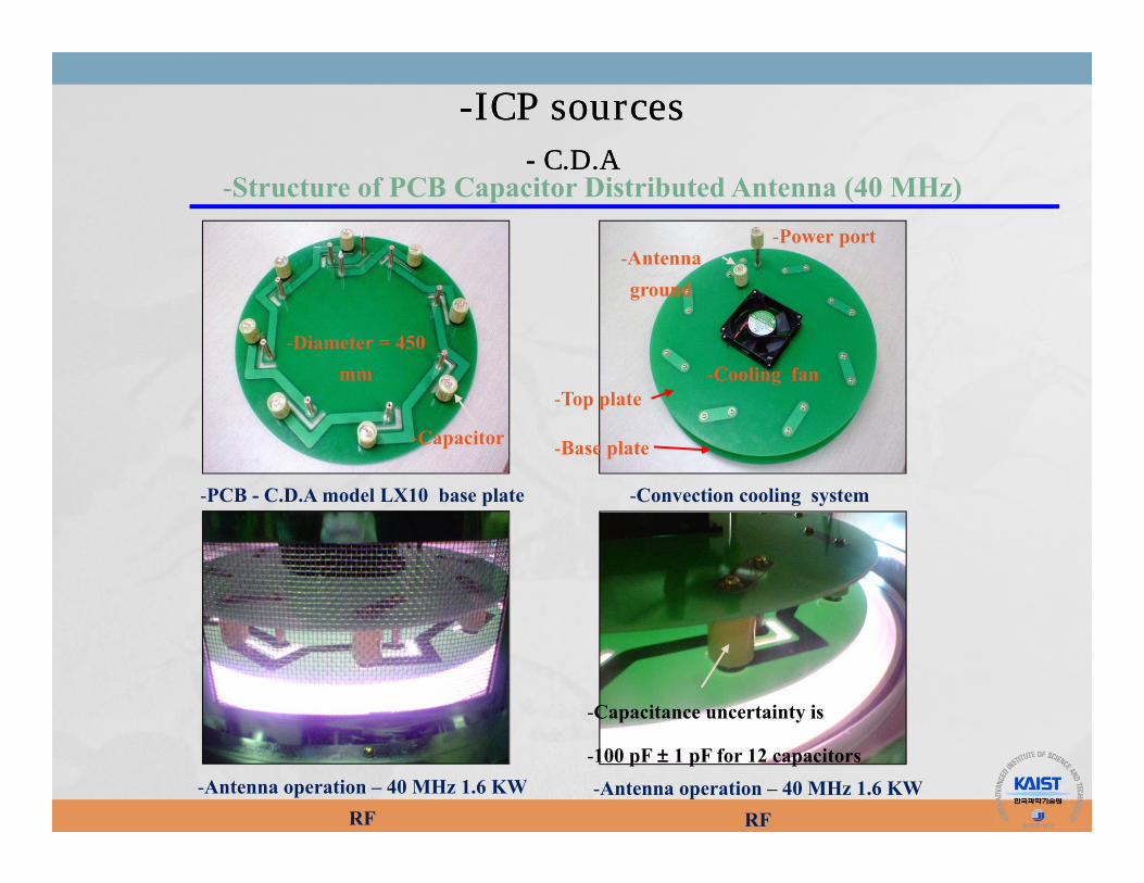
-PCB - C.D.A model LX10 base plate
-Antenna operation – 40 MHz 1.6 KW RF
-Convection cooling system
-Cooling fan-Diameter = 450
mm
-Capacitor
-Antenna operation – 40 MHz 1.6 KW RF
-Power port-Antenna ground
-Capacitance uncertainty is
-100 pF ± 1 pF for 12 capacitors
-Top plate
-Base plate
-ICP sources - C.D.A
-ICP sources - C.D.A
-Structure of PCB Capacitor Distributed Antenna (40 MHz)

Asymmetry Factors and Uniformity
1Antenna coil
properties
• Coil plasma capacitive coupling coil termination impedance azimuth
coil current asymmetric E-field
• Coil E-field asymmetry (1-turn coil 5-turn coil symmetric)
• Asymmetric E-field ion flux uniformity
2 Reactor Structure • Wafer clamp support load-lock bay asymmetry (check)
3 Gas Pumping• One-side pumping asymmetric pumping asymmetry
• Neutral species (ion flux ambipolar transport)
4 Gas Injection • Nozzle neutral asymmetry (showerhead radial jet)
5 Wall Reactive • Wall reactivity radical wall loss uniformity (gas species)
6 Gas Pressure• Neutral species pressure dependence
• Ion flux pressure
2
a izn D n nt
~
aa
DD n n ~
aiz
D 3~ 5eT eV 5P mTorr
1/2~ ( ) ~5
a
iz
D cm Scale length 5cm
Asymmetry FactorsAsymmetry Factors

-41
Summary
1. Standing wave effect and skin effect should be considered in large area plasma source
2. RF phase shift or modulation control uniformity.3. Multi-feeding is also a method for uniformity control.4. Multi-plasma sources(multiple helicon or multi-electrode
CCP) can be used to increase plasma uniformity.5. Stray capacitance should be considered in plasma system
design.6. Asymmetry factors be taken into account plasma uniformity.


![78 REFERENCES [1] Chen K.J, Hung F.Y, Chang S.J, and Young ...](https://static.fdocuments.in/doc/165x107/58947ad51a28ab3a358bfbed/78-references-1-chen-kj-hung-fy-chang-sj-and-young-.jpg)