Design considerations of Paralleled GaN HEMT -based Half ...
High-voltage GaN-HEMT devices,
simulation and modelling
Stephen Sque, NXP Semiconductors
ESSDERC 2013
Bucharest, Romania
16th September 2013

PUBLIC
Outline
GaN and related materials
The AlGaN/GaN heterostructure
GaN wafers
GaN devices
Issues facing high-voltage GaN-HEMT development
High-voltage breakdown
GaN-HEMT device simulation
Compact modelling of GaN HEMTs
Summary and conclusion
16th September 2013 Stephen Sque - ESSDERC tutorial
2

PUBLIC
Outline
GaN and related materials
The AlGaN/GaN heterostructure
GaN wafers
GaN devices
Issues facing high-voltage GaN-HEMT development
High-voltage breakdown
GaN-HEMT device simulation
Compact modelling of GaN HEMTs
Summary and conclusion
16th September 2013 Stephen Sque - ESSDERC tutorial
3

PUBLIC
Gallium nitride
Gallium nitride (GaN) is a binary III-V compound material, with:
– Wurtzite (hexagonal) crystal structure
– Wide band gap of 3.4 eV (direct)
– High thermal conductivity
16th September 2013 Stephen Sque - ESSDERC tutorial
4
Ga
N
III IV V

PUBLIC
Properties of GaN
Selected properties at 300 K:
16th September 2013 Stephen Sque - ESSDERC tutorial
5
Property Si 4H-SiC Diamond GaAs GaN
Band gap (eV) 1.1 3.2 5.5 1.4 3.4
Relative permittivity 11.9 10 5.5 12.5 9–10
Breakdown field (MV/cm) 0.3 3 5 0.4 3
Thermal conductivity (W/K/cm) 1.48 3.30 20.00+ 0.54 1.30
PUBLIC
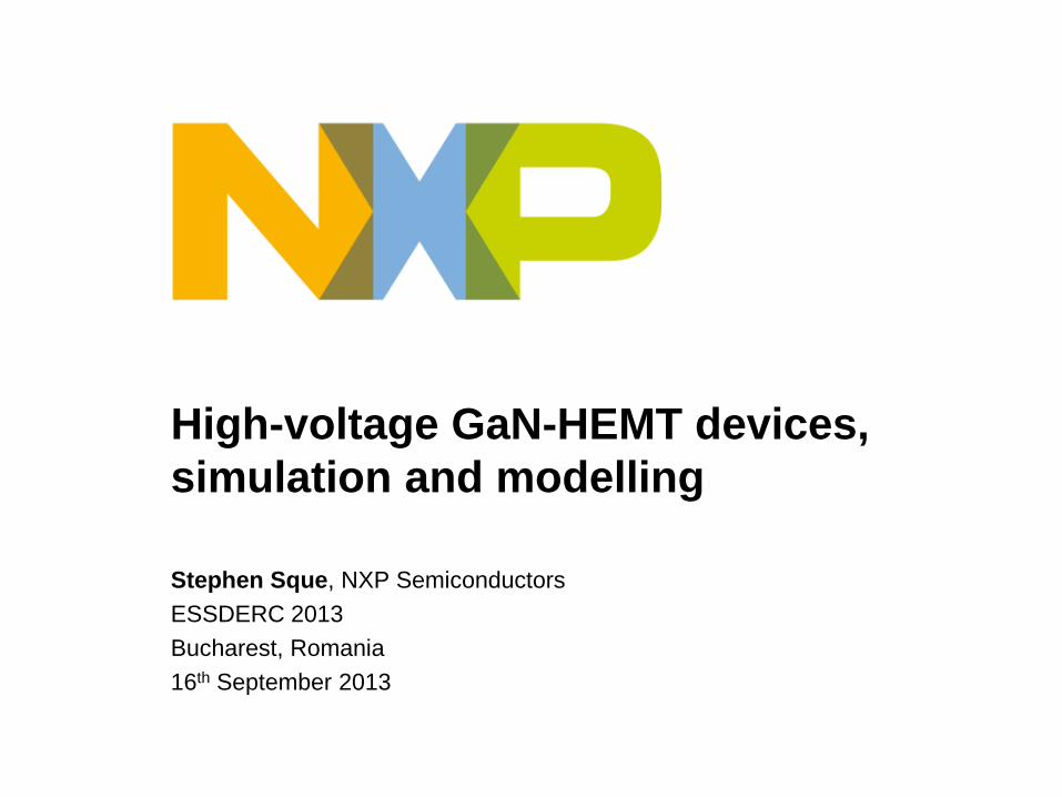
Aluminium nitride
Aluminium nitride (AlN) is a binary III-V compound material, with:
– Wurtzite (hexagonal) crystal structure
– Wide band gap of 6.2 eV (direct)
– High thermal conductivity
16th September 2013 Stephen Sque - ESSDERC tutorial
6
Al
N
III IV V

PUBLIC
AlGaN
Take GaN and replace a fraction x (the mole fraction) of the Ga atoms
with Al atoms AlxGa1−xN
Most material properties are then intermediate between those
of GaN and AlN
16th September 2013 Stephen Sque - ESSDERC tutorial
7
Quantity GaN Al0.2Ga0.8N AlN Units Interpolation
Band gap 3.43 3.77 6.20 eV Bowed, factor −1.33
Breakdown field 3.3 4.32 8.4 MV/cm Linear (?)
Relative permittivity 9.5 9.3 8.5 Linear
[R. Quay, Gallium Nitride Electronics, ISBN 978-3-540-71890-1]
PUBLIC
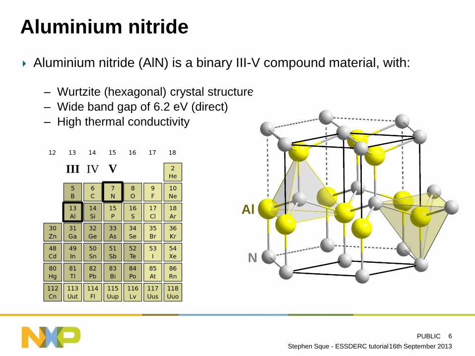
GaN crystal growth
Convention: [0001] direction
is along c axis from Ga to N
A-face: atom of type A
is on top of bilayer
Single-bond
(low energy)
surface
16th September 2013 Stephen Sque - ESSDERC tutorial
8
[O. Ambacher et al., J. Appl. Phys. 85 (6), 3222 (1999)]
bilayer
PUBLIC
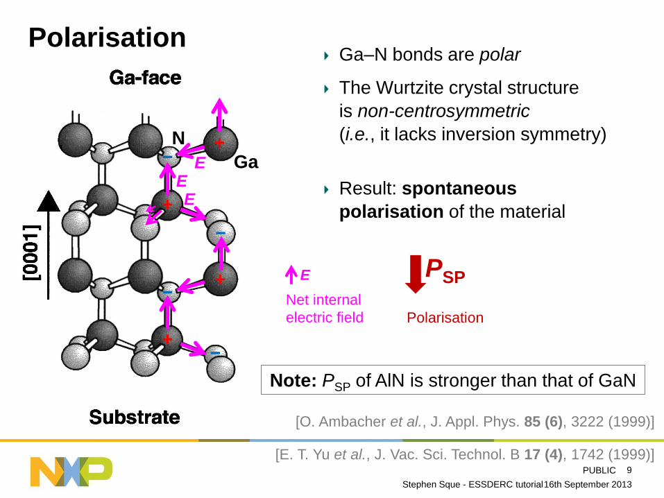
Polarisation Ga–N bonds are polar
The Wurtzite crystal structure
is non-centrosymmetric
(i.e., it lacks inversion symmetry)
Result: spontaneous
polarisation of the material
16th September 2013 Stephen Sque - ESSDERC tutorial
9
−
+ −
+
−
+
Ga
N +
−
E
Net internal
electric field
PSP
Polarisation
[O. Ambacher et al., J. Appl. Phys. 85 (6), 3222 (1999)]
Note: PSP of AlN is stronger than that of GaN
[E. T. Yu et al., J. Vac. Sci. Technol. B 17 (4), 1742 (1999)]
E E E
PUBLIC
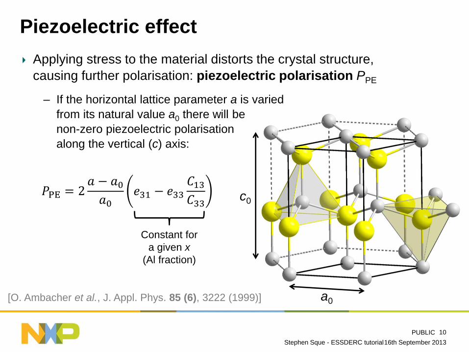
Piezoelectric effect
Applying stress to the material distorts the crystal structure,
causing further polarisation: piezoelectric polarisation PPE
– If the horizontal lattice parameter a is varied
from its natural value a0 there will be
non-zero piezoelectric polarisation
along the vertical (c) axis:
16th September 2013 Stephen Sque - ESSDERC tutorial
10
a0
c0 𝑃PE = 2
𝑎 − 𝑎0𝑎0
𝑒31 − 𝑒33𝐶13𝐶33
Constant for
a given x
(Al fraction)
[O. Ambacher et al., J. Appl. Phys. 85 (6), 3222 (1999)]
PUBLIC
Outline
GaN and related materials
The AlGaN/GaN heterostructure
GaN wafers
GaN devices
Issues facing high-voltage GaN-HEMT development
High-voltage breakdown
GaN-HEMT device simulation
Compact modelling of GaN HEMTs
Summary and conclusion
16th September 2013 Stephen Sque - ESSDERC tutorial
11

PUBLIC
The AlGaN/GaN heterostructure
AlN has a smaller lattice constant a0 than GaN
…and more spontaneous polarisation PSP
Grow AlxGa1−xN on top of (relaxed) GaN:
16th September 2013 Stephen Sque - ESSDERC tutorial
12
AlxGa1−xN
GaN
PSP
PSP
AlxGa1−xN
GaN
PSP
PSP
PPE
+ + + + + + + + + + + + + Net positive
polarisation-induced
sheet charge
PUBLIC
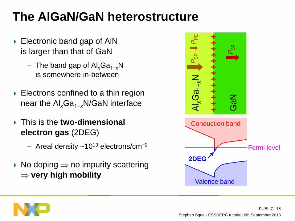
The AlGaN/GaN heterostructure
Electronic band gap of AlN
is larger than that of GaN
– The band gap of AlxGa1−xN
is somewhere in-between
Electrons confined to a thin region
near the AlxGa1−xN/GaN interface
This is the two-dimensional
electron gas (2DEG)
– Areal density ~1013 electrons/cm−2
No doping no impurity scattering
very high mobility
16th September 2013 Stephen Sque - ESSDERC tutorial
13
Fermi level
Conduction band
Valence band
2DEG

PUBLIC
Formation of the 2DEG
Where do the electrons for the 2DEG “come from”?
Model: donor-like surface states “provide” electrons
16th September 2013 Stephen Sque - ESSDERC tutorial
14
[J. P. Ibbetson et al., Appl. Phys. Lett. 77 (2), 250 (2000)]
Theory Measurements
Strain
relaxation
Electrons can come
from Ohmic contacts.
Surface donors play a
role in the electrostatics.
PUBLIC
Outline
GaN and related materials
The AlGaN/GaN heterostructure
GaN wafers
GaN devices
Issues facing high-voltage GaN-HEMT development
High-voltage breakdown
GaN-HEMT device simulation
Compact modelling of GaN HEMTs
Summary and conclusion
16th September 2013 Stephen Sque - ESSDERC tutorial
15
PUBLIC
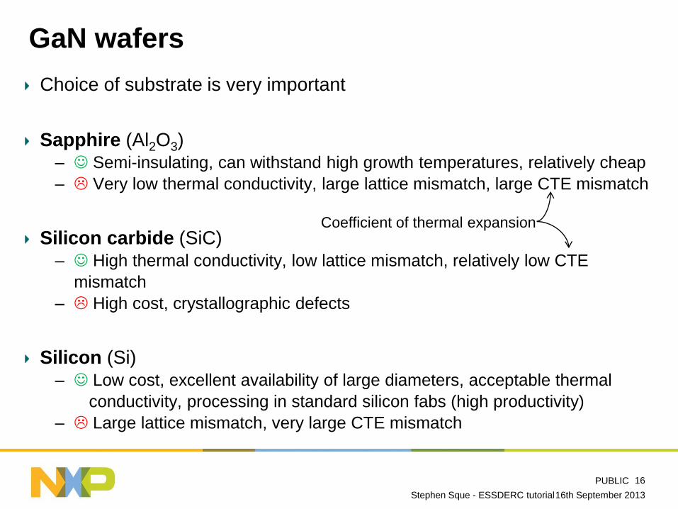
GaN wafers
Choice of substrate is very important
Sapphire (Al2O3) – Semi-insulating, can withstand high growth temperatures, relatively cheap
– Very low thermal conductivity, large lattice mismatch, large CTE mismatch
Silicon carbide (SiC) – High thermal conductivity, low lattice mismatch, relatively low CTE
mismatch
– High cost, crystallographic defects
Silicon (Si) – Low cost, excellent availability of large diameters, acceptable thermal
conductivity, processing in standard silicon fabs (high productivity)
– Large lattice mismatch, very large CTE mismatch
16th September 2013 Stephen Sque - ESSDERC tutorial
16
Coefficient of thermal expansion

PUBLIC
GaN-on-Si wafers
Base: silicon substrate
with (111) face
Example recipe: 1. Thin seed layer of AlN
2. Thick buffer layer:
superlattice of alternating
GaN and AlGaN layers
3. High-quality GaN layer
4. AlGaN barrier
5. GaN cap layer
Reduce dislocation density
Stress control / wafer bow
16th September 2013 Stephen Sque - ESSDERC tutorial
17
[H. F. Liu et al., J. Appl. Phys. 113, 023510 (2013)]
[S. Lenci et al., Elec. Dev. Lett. 34 (8), 1035 (2013)]
[D. Marcon et al., Trans. Semi. Manu. 26 (3), 361 (2013)]

PUBLIC
Dislocations
High initial dislocation density reduced towards surface (2DEG)
by optimisation of buffer design
16th September 2013 Stephen Sque - ESSDERC tutorial
18
[S. L. Selvaraj et al., Proc. DRC 2012, 53 (2012)]
Dislocations ~109 cm−2

PUBLIC
Outline
GaN and related materials
The AlGaN/GaN heterostructure
GaN wafers
GaN devices
Issues facing high-voltage GaN-HEMT development
High-voltage breakdown
GaN-HEMT device simulation
Compact modelling of GaN HEMTs
Summary and conclusion
16th September 2013 Stephen Sque - ESSDERC tutorial
19

PUBLIC
GaN devices High–electron-mobility transistor (HEMT)
Ohmic contacts
to 2DEG (Ti/Al)
Source and drain
metallisation (Al)
Gate metal (Ni)
on top of GaN cap
– Schottky contact
SiN passivation
Metal field plate(s)
16th September 2013 Stephen Sque - ESSDERC tutorial
20 NXP process: [J. J. T. M. Donkers et al., CS-MANTECH 2013, 259]
foot
head
PUBLIC
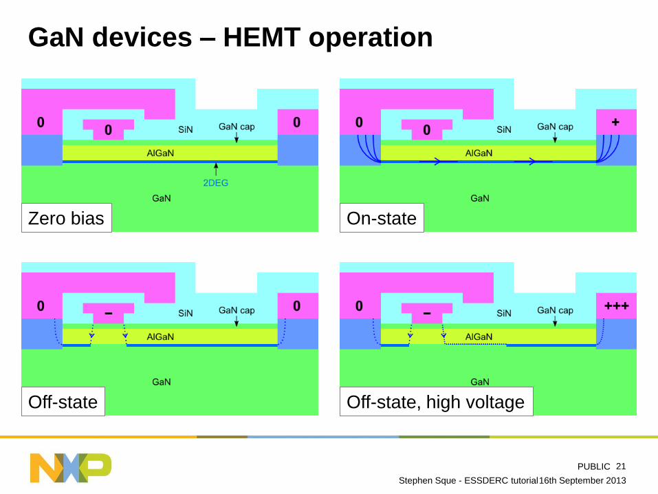
GaN devices – HEMT operation
16th September 2013 Stephen Sque - ESSDERC tutorial
21
Zero bias On-state
Off-state Off-state, high voltage

PUBLIC
GaN devices Schottky barrier diode (SBD)
“HEMT without a source”
“Gate” → anode – Longer to handle
high current
“Drain” → cathode
16th September 2013 Stephen Sque - ESSDERC tutorial
22
PUBLIC
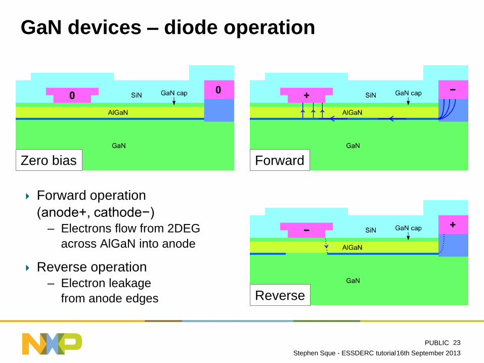
GaN devices – diode operation
16th September 2013 Stephen Sque - ESSDERC tutorial
23
Zero bias Forward
Reverse
Forward operation
(anode+, cathode−) – Electrons flow from 2DEG
across AlGaN into anode
Reverse operation – Electron leakage
from anode edges
PUBLIC
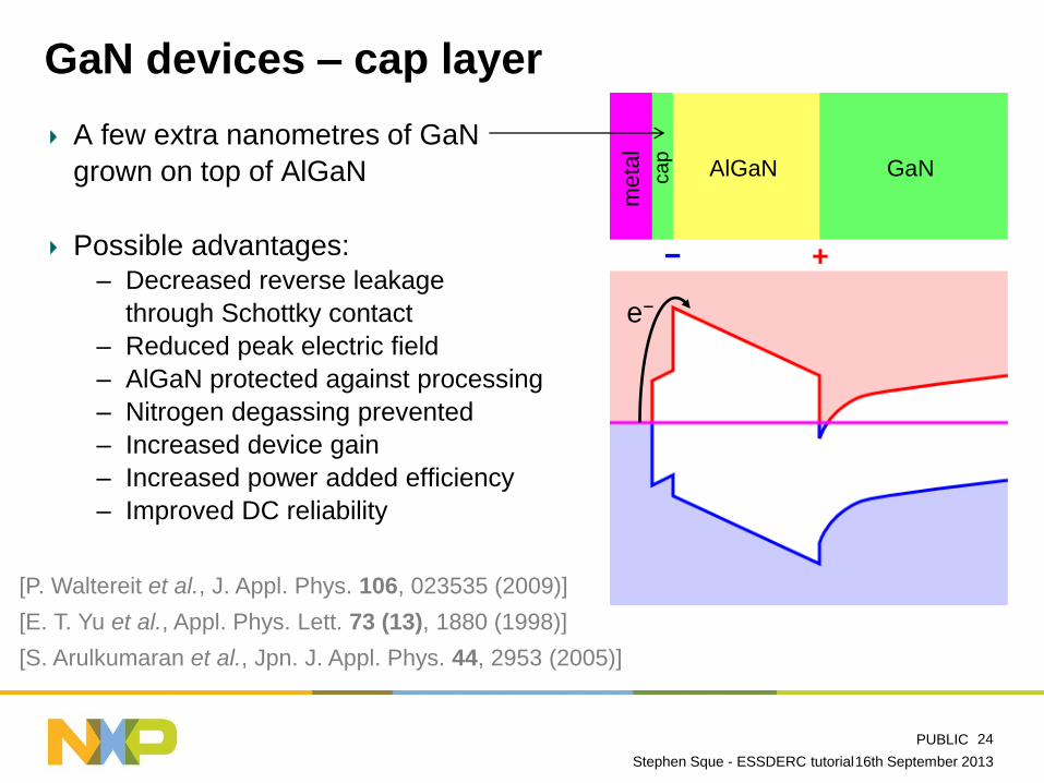
GaN devices – cap layer
A few extra nanometres of GaN
grown on top of AlGaN
Possible advantages: – Decreased reverse leakage
through Schottky contact
– Reduced peak electric field
– AlGaN protected against processing
– Nitrogen degassing prevented
– Increased device gain
– Increased power added efficiency
– Improved DC reliability
16th September 2013 Stephen Sque - ESSDERC tutorial
24
[E. T. Yu et al., Appl. Phys. Lett. 73 (13), 1880 (1998)] m
eta
l
cap
AlGaN GaN
+ −
e−
[P. Waltereit et al., J. Appl. Phys. 106, 023535 (2009)]
[S. Arulkumaran et al., Jpn. J. Appl. Phys. 44, 2953 (2005)]
PUBLIC
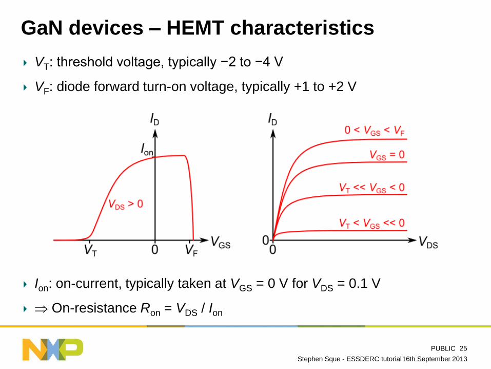
GaN devices – HEMT characteristics
VT: threshold voltage, typically −2 to −4 V
VF: diode forward turn-on voltage, typically +1 to +2 V
Ion: on-current, typically taken at VGS = 0 V for VDS = 0.1 V
On-resistance Ron = VDS / Ion
16th September 2013 Stephen Sque - ESSDERC tutorial
25
PUBLIC
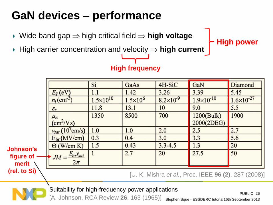
GaN devices – performance
Wide band gap high critical field high voltage
High carrier concentration and velocity high current
16th September 2013 Stephen Sque - ESSDERC tutorial
26
[U. K. Mishra et al., Proc. IEEE 96 (2), 287 (2008)]
High power
High frequency
Johnson’s
figure of
merit
(rel. to Si)
[A. Johnson, RCA Review 26, 163 (1965)]
Suitability for high-frequency power applications

PUBLIC
GaN devices – performance
16th September 2013 Stephen Sque - ESSDERC tutorial
27
[N. Ikeda et al., Proc. IEEE 98 (7), 1151 (2010)]
Baliga figure of merit
– Based on minimising the conduction losses in power FETs
– Assumes power losses are solely due to the on-state power dissipation
– Applies to lower frequencies where conduction losses dominate
[B. J. Baliga, Elec. Dev. Lett. 10 (10), 455 (1989)]
Relative
permittivity
Carrier mobility
BFOM = εr µ Ec3
Critical electric
field
Sometimes Eg is used!
PUBLIC
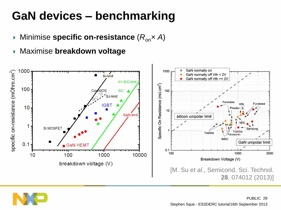
GaN devices – benchmarking
Minimise specific on-resistance (Ron× A)
Maximise breakdown voltage
16th September 2013 Stephen Sque - ESSDERC tutorial
28
[M. Su et al., Semicond. Sci. Technol.
28, 074012 (2013)]

PUBLIC
GaN devices – benchmarking
Some more specific–on-resistance vs. breakdown-voltage plots
16th September 2013 Stephen Sque - ESSDERC tutorial
29
[S. L. Selvaraj et al., Proc. DRC 2012, 53] [N. Ikeda et al., Proc. ISPSD 2011, 284]
See also [Q. Jiang et al., EDL 34 (3), 357 (2013)] and
[Z. Tang et al., EDL 34 (3), 366 (2013)]
PUBLIC
Outline
GaN and related materials
The AlGaN/GaN heterostructure
GaN wafers
GaN devices
Issues facing high-voltage GaN-HEMT development
High-voltage breakdown
GaN-HEMT device simulation
Compact modelling of GaN HEMTs
Summary and conclusion
16th September 2013 Stephen Sque - ESSDERC tutorial
30
PUBLIC
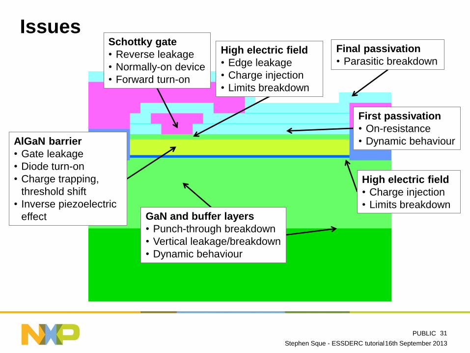
Issues
16th September 2013 Stephen Sque - ESSDERC tutorial
31
Schottky gate
• Reverse leakage
• Normally-on device
• Forward turn-on
High electric field
• Edge leakage
• Charge injection
• Limits breakdown
First passivation
• On-resistance
• Dynamic behaviour AlGaN barrier
• Gate leakage
• Diode turn-on
• Charge trapping,
threshold shift
• Inverse piezoelectric
effect GaN and buffer layers
• Punch-through breakdown
• Vertical leakage/breakdown
• Dynamic behaviour
High electric field
• Charge injection
• Limits breakdown
Final passivation
• Parasitic breakdown

PUBLIC
Issues – gate leakage
Various mechanisms potentially involved in gate leakage
16th September 2013 Stephen Sque - ESSDERC tutorial
32
[B. S. Eller et al., J. Vac. Sci. Technol. A 31 (5), 050807 (2013)]
VG < 0 2DEG
See also [L. Xia et al., Appl. Phys. Lett. 102 (11), 113510 (2013)]
AlGaN
d
^
PUBLIC
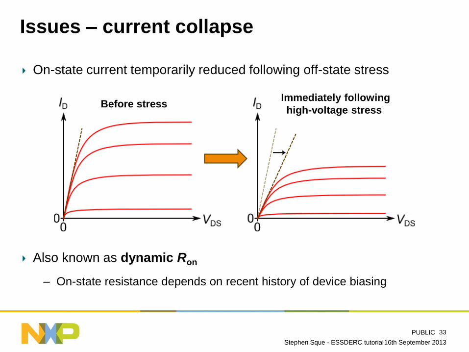
Issues – current collapse
On-state current temporarily reduced following off-state stress
Also known as dynamic Ron
– On-state resistance depends on recent history of device biasing
16th September 2013 Stephen Sque - ESSDERC tutorial
33
Before stress Immediately following
high-voltage stress

PUBLIC
Issues – current collapse
Device design and substrate composition can have a strong influence
on the magnitude of current collapse (dynamic-Ron increase)
16th September 2013 Stephen Sque - ESSDERC tutorial
34
[O. Hilt et al., Proc. ISPSD 2012, 345 (2012)]
0 V
30 V
50 V
65 V
Off-state
stress:
Also [S. DasGupta et al., Appl. Phys. Lett. 101 (24), 243506 (2012)]

PUBLIC
Issues – virtual-gate effect
Off-state stress: – Electrons from gate injected
into trap states next to gate
On-state after stress: – Trapped electrons act like
a negatively biased gate
– 2DEG partially depleted
underneath increased Ron
Later (~seconds): – Electrons de-trap,
2DEG current restored
16th September 2013 Stephen Sque - ESSDERC tutorial
35
On-state following stress
Off-state stress
− − − −
− − − −
Thinned
2DEG
Injected
electrons
[R. Vetury et al., Trans. Elec. Dev. 48 (3), 560 (2001)]
[T. Mizutani et al., TED 50, 2015 (2003)]
PUBLIC
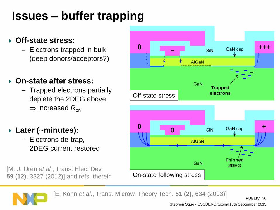
Issues – buffer trapping
Off-state stress: – Electrons trapped in bulk
(deep donors/acceptors?)
On-state after stress: – Trapped electrons partially
deplete the 2DEG above
increased Ron
Later (~minutes): – Electrons de-trap,
2DEG current restored
16th September 2013 Stephen Sque - ESSDERC tutorial
36
[M. J. Uren et al., Trans. Elec. Dev.
59 (12), 3327 (2012)] and refs. therein On-state following stress
Off-state stress
Thinned
2DEG
Trapped
electrons
−
− − −
− − −
[E. Kohn et al., Trans. Microw. Theory Tech. 51 (2), 634 (2003)]
− − −
− − −

PUBLIC
Issues – inverse piezoelectric effect
Piezoelectric effect:
mechanical stress polarisation (i.e., internal electric field)
Inverse (or converse) piezoelectric effect:
applied voltage electric field
mechanical stress
High field at drain-side edge of gate
local stress defect formation
device degradation (reliability) – Mitigate with field-plate design →
– Not the full story… See [Meneghesso / Meneghini / Zanoni]
16th September 2013 Stephen Sque - ESSDERC tutorial
37 Also [N. A. Mahadik et al., Appl. Phys. Lett. 93 (26), 262106 (2008)]
[Y. Ando et al., TED 59 (12), 3350 (2012)]
[J. Joh et al., Microelec. Reliab. 50 (6), 767 (2010)]

PUBLIC
Outline
GaN and related materials
The AlGaN/GaN heterostructure
GaN wafers
GaN devices
Issues facing high-voltage GaN-HEMT development
High-voltage breakdown
GaN-HEMT device simulation
Compact modelling of GaN HEMTs
Summary and conclusion
16th September 2013 Stephen Sque - ESSDERC tutorial
38
PUBLIC
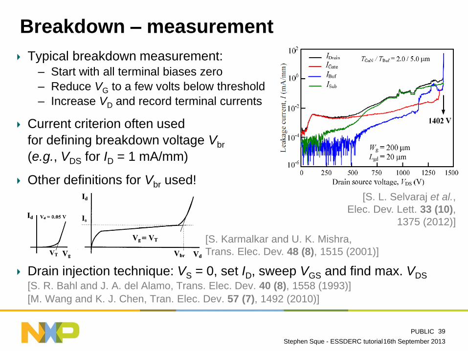
Breakdown – measurement
Typical breakdown measurement: – Start with all terminal biases zero
– Reduce VG to a few volts below threshold
– Increase VD and record terminal currents
Current criterion often used
for defining breakdown voltage Vbr
(e.g., VDS for ID = 1 mA/mm)
Other definitions for Vbr used!
Drain injection technique: VS = 0, set ID, sweep VGS and find max. VDS [S. R. Bahl and J. A. del Alamo, Trans. Elec. Dev. 40 (8), 1558 (1993)]
[M. Wang and K. J. Chen, Tran. Elec. Dev. 57 (7), 1492 (2010)]
16th September 2013 Stephen Sque - ESSDERC tutorial
39
[S. L. Selvaraj et al.,
Elec. Dev. Lett. 33 (10),
1375 (2012)]
[S. Karmalkar and U. K. Mishra,
Trans. Elec. Dev. 48 (8), 1515 (2001)]

PUBLIC
Breakdown – mechanisms
Extrinsic: air arcing, conductive surface layer
Intrinsic: impact ionisation, punch-through, vertical breakdown
16th September 2013 Stephen Sque - ESSDERC tutorial
40
Arcing (parasitic)
Punch-through
Vertical
leakage
Impact ionisation
?

PUBLIC
Breakdown – mechanisms
Compare terminal currents to assess the
relative contributions of different physical
mechanisms to breakdown
Example using current criterion for breakdown:
16th September 2013 Stephen Sque - ESSDERC tutorial
41
Dominated by
gate-leakage
impact-ionisation
Dominated by
drain-to-source
punch-through
Dominated by
vertical current
“Chuck”
(substrate)

PUBLIC
Breakdown – punch-through
At high drain biases in the off-state, electrons can travel through the bulk
GaN underneath the (turned-off) gate drain-to-source current
Prevent using: longer gate, acceptor doping in the bulk, back barrier, …
16th September 2013 Stephen Sque - ESSDERC tutorial
42 [M. J. Uren et al., Trans. Elec. Dev. 53 (2), 395 (2006)]
2DEG 2DEG

PUBLIC
Breakdown – impact ionisation
Impact ionisation: high-energy electrons (or holes) can knock other
electrons out of valence-band states into conduction-band states,
creating electron-hole pairs and hence raising the current
Avalanche breakdown: every electron (or hole) creates another
electron-hole pair, and the current grows uncontrollably
16th September 2013 Stephen Sque - ESSDERC tutorial
43

PUBLIC
Breakdown – impact ionisation
Positive temperature coefficient: Vbr increases with increasing T
suggests impact ionisation (increased phonon scattering)
[N. Dyakonova et al., Electron. Lett. 34 (17), 1699 (1998)]
[T. Nakao et al., Phys. Stat. Sol. (c) 0 (7), 2335 (2003)]
[M. Wang and K. J. Chen, TED 57 (7), 1492 (2010)]
[X. Z. Dang et al., Electron. Lett. 35 (7), 602 (1999)]
[B. Brar et al., Proc. HPD 2002, 487 (2002)]
Impact-ionisation parameters for GaN
have been evaluated theoretically
[J. Kolník et al., J. Appl. Phys. 81 (2), 726 (1997)]
[F. Bertazzi et al., J. Appl. Phys. 106, 063718 (2009)]
…and determined experimentally
[K. Kunihiro et al., EDL 20 (12), 608 (1999)]
16th September 2013 Stephen Sque - ESSDERC tutorial
44
[N. Dyakonova et al.,
Appl. Phys. Lett. 72 (10), 2562 (1998)]
Not the full story? See also [Meneghesso / Meneghini / Zanoni]

PUBLIC
Breakdown – gate-to-drain length scaling
Breakdown voltage Vbr scales with gate-to-drain length LGD
until vertical breakdown becomes dominant
Why is ΔVbr / ΔLGD < 3 MV/cm? – leakage, electric field peaks, etc.…
16th September 2013 Stephen Sque - ESSDERC tutorial
45
[H. Ueda et al., Proc. ISPSD 2005, 311 (2005)] [S. L. Selvaraj et al., EDL 33 (10), 1375 (2012)]
~1 MV/cm
See also [N. Ikeda et al., Proc. IEEE 98 (7), 1151 (2010)]
PUBLIC
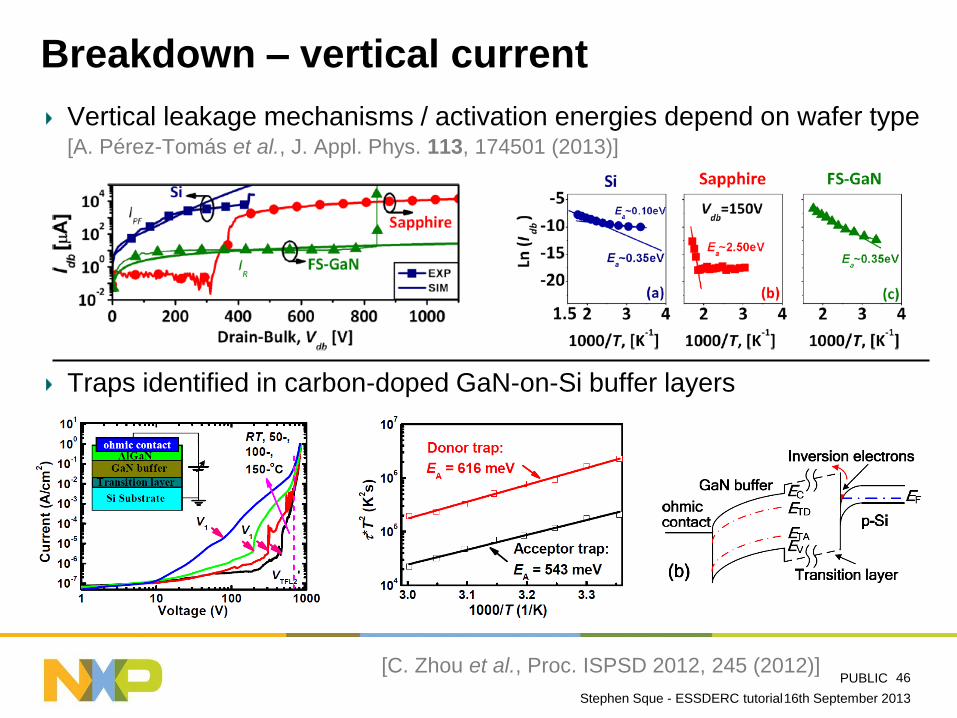
Breakdown – vertical current
Vertical leakage mechanisms / activation energies depend on wafer type [A. Pérez-Tomás et al., J. Appl. Phys. 113, 174501 (2013)]
Traps identified in carbon-doped GaN-on-Si buffer layers
16th September 2013 Stephen Sque - ESSDERC tutorial
46 [C. Zhou et al., Proc. ISPSD 2012, 245 (2012)]

PUBLIC
Breakdown – buffer optimisation
Increasing the thickness of the buffer can increase breakdown voltage
due to improved material quality and reduced vertical leakage [S. L. Selvaraj et al., Elec. Dev. Lett. 33 (10), 1375 (2012)] (see earlier slide)
The inclusion of a carbon-doped “back barrier” can postpone punch-
through to higher VDS (at the expense of increased on-resistance) [E. Bahat-Treidel et al., Trans. Elec. Dev. 57 (11), 3050 (2010)]
[S. A. Chevtchenko et al., Appl. Phys. Lett. 100, 223502 (2012)] ↓
16th September 2013 Stephen Sque - ESSDERC tutorial
47 See also [N. Ikeda et al., Proc. IEEE 98 (7), 1151 (2010)]
Measurements Simulations
Different buffer compositions
PUBLIC
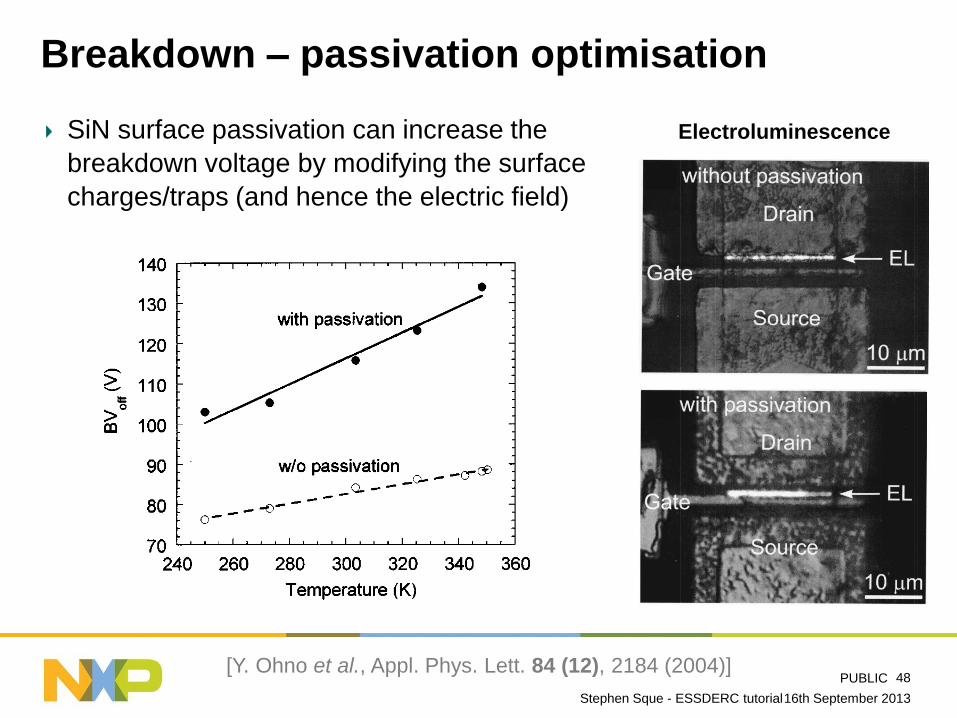
Breakdown – passivation optimisation
SiN surface passivation can increase the
breakdown voltage by modifying the surface
charges/traps (and hence the electric field)
16th September 2013 Stephen Sque - ESSDERC tutorial
48 [Y. Ohno et al., Appl. Phys. Lett. 84 (12), 2184 (2004)]
Electroluminescence

PUBLIC
Outline
GaN and related materials
The AlGaN/GaN heterostructure
GaN wafers
GaN devices
Issues facing high-voltage GaN-HEMT development
High-voltage breakdown
GaN-HEMT device simulation
Compact modelling of GaN HEMTs
Summary and conclusion
16th September 2013 Stephen Sque - ESSDERC tutorial
49
PUBLIC
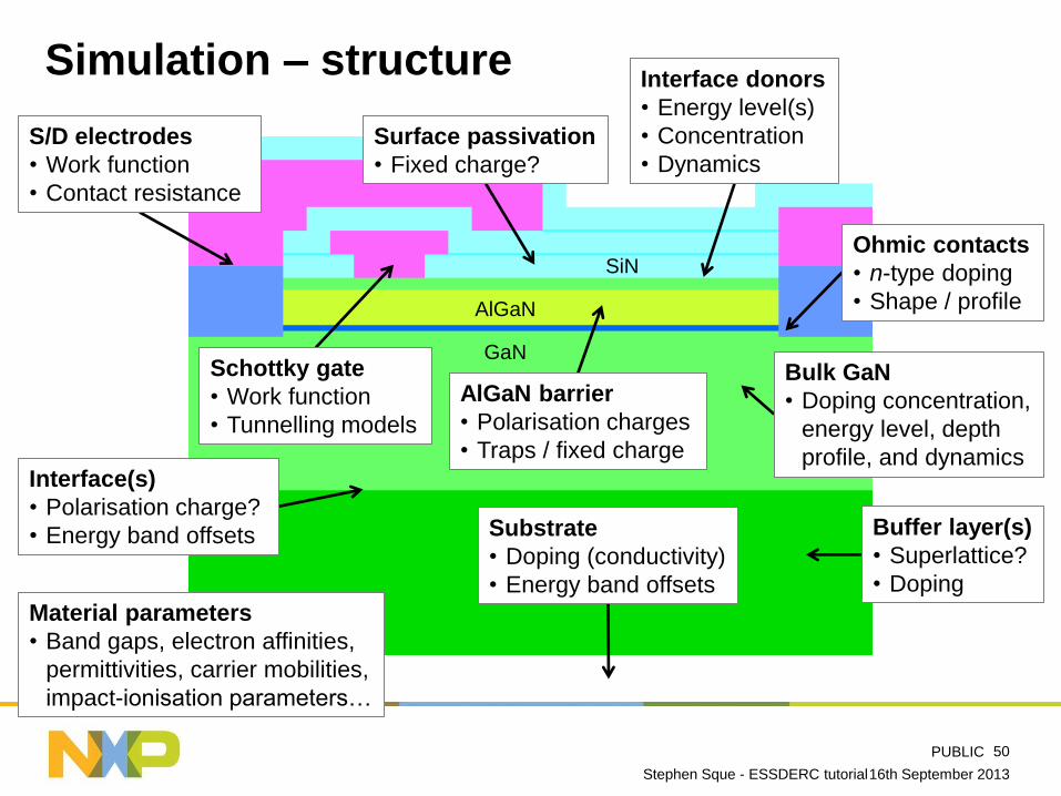
Simulation – structure
16th September 2013 Stephen Sque - ESSDERC tutorial
50
Ohmic contacts
• n-type doping
• Shape / profile
Interface donors
• Energy level(s)
• Concentration
• Dynamics
Surface passivation
• Fixed charge?
Schottky gate
• Work function
• Tunnelling models
S/D electrodes
• Work function
• Contact resistance
AlGaN barrier
• Polarisation charges
• Traps / fixed charge
Bulk GaN
• Doping concentration,
energy level, depth
profile, and dynamics
Buffer layer(s)
• Superlattice?
• Doping
Interface(s)
• Polarisation charge?
• Energy band offsets Substrate
• Doping (conductivity)
• Energy band offsets
Material parameters
• Band gaps, electron affinities,
permittivities, carrier mobilities,
impact-ionisation parameters…
AlGaN
GaN
SiN
PUBLIC
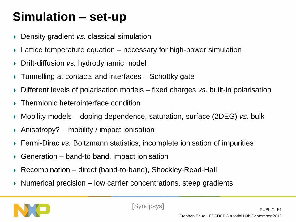
Simulation – set-up
Density gradient vs. classical simulation
Lattice temperature equation – necessary for high-power simulation
Drift-diffusion vs. hydrodynamic model
Tunnelling at contacts and interfaces – Schottky gate
Different levels of polarisation models – fixed charges vs. built-in polarisation
Thermionic heterointerface condition
Mobility models – doping dependence, saturation, surface (2DEG) vs. bulk
Anisotropy? – mobility / impact ionisation
Fermi-Dirac vs. Boltzmann statistics, incomplete ionisation of impurities
Generation – band-to band, impact ionisation
Recombination – direct (band-to-band), Shockley-Read-Hall
Numerical precision – low carrier concentrations, steep gradients
16th September 2013 Stephen Sque - ESSDERC tutorial
51 [Synopsys]
PUBLIC
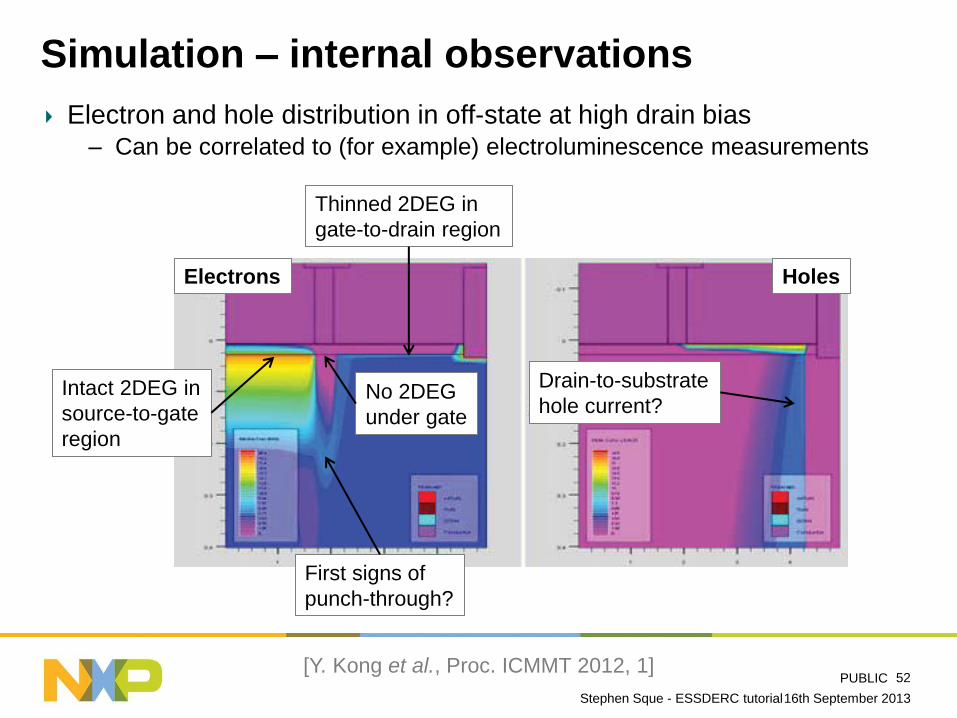
Simulation – internal observations
Electron and hole distribution in off-state at high drain bias – Can be correlated to (for example) electroluminescence measurements
16th September 2013 Stephen Sque - ESSDERC tutorial
52 [Y. Kong et al., Proc. ICMMT 2012, 1]
Electrons Holes
Intact 2DEG in
source-to-gate
region
Thinned 2DEG in
gate-to-drain region
No 2DEG
under gate
First signs of
punch-through?
Drain-to-substrate
hole current?
PUBLIC
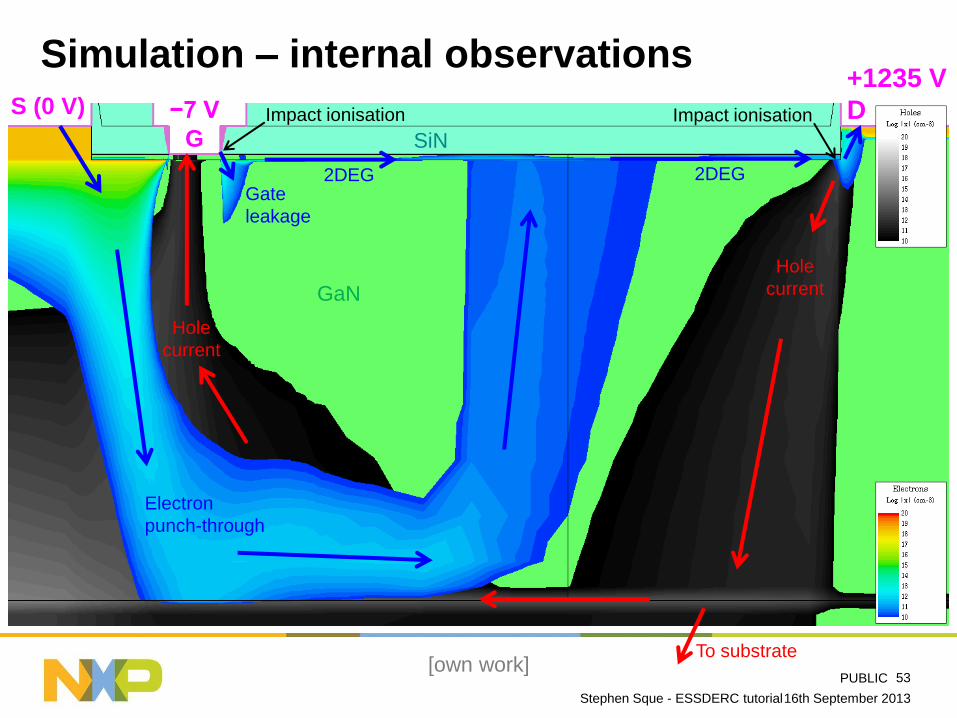
Simulation – internal observations
16th September 2013 Stephen Sque - ESSDERC tutorial
53 [own work]
−7 V
G
+1235 V
D S (0 V)
Hole
current
Hole
current
Electron
punch-through
2DEG 2DEG
Impact ionisation Impact ionisation
To substrate
Gate
leakage
GaN
SiN
PUBLIC
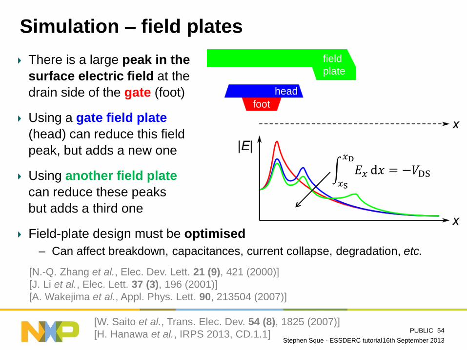
Simulation – field plates
There is a large peak in the
surface electric field at the
drain side of the gate (foot)
Using a gate field plate
(head) can reduce this field
peak, but adds a new one
Using another field plate
can reduce these peaks
but adds a third one
Field-plate design must be optimised
– Can affect breakdown, capacitances, current collapse, degradation, etc.
16th September 2013 Stephen Sque - ESSDERC tutorial
54
𝐸𝑥
𝑥D
𝑥S
d𝑥 = −𝑉DS
[N.-Q. Zhang et al., Elec. Dev. Lett. 21 (9), 421 (2000)]
[J. Li et al., Elec. Lett. 37 (3), 196 (2001)]
[A. Wakejima et al., Appl. Phys. Lett. 90, 213504 (2007)]
[W. Saito et al., Trans. Elec. Dev. 54 (8), 1825 (2007)]
[H. Hanawa et al., IRPS 2013, CD.1.1]
foot
head
field
plate
PUBLIC
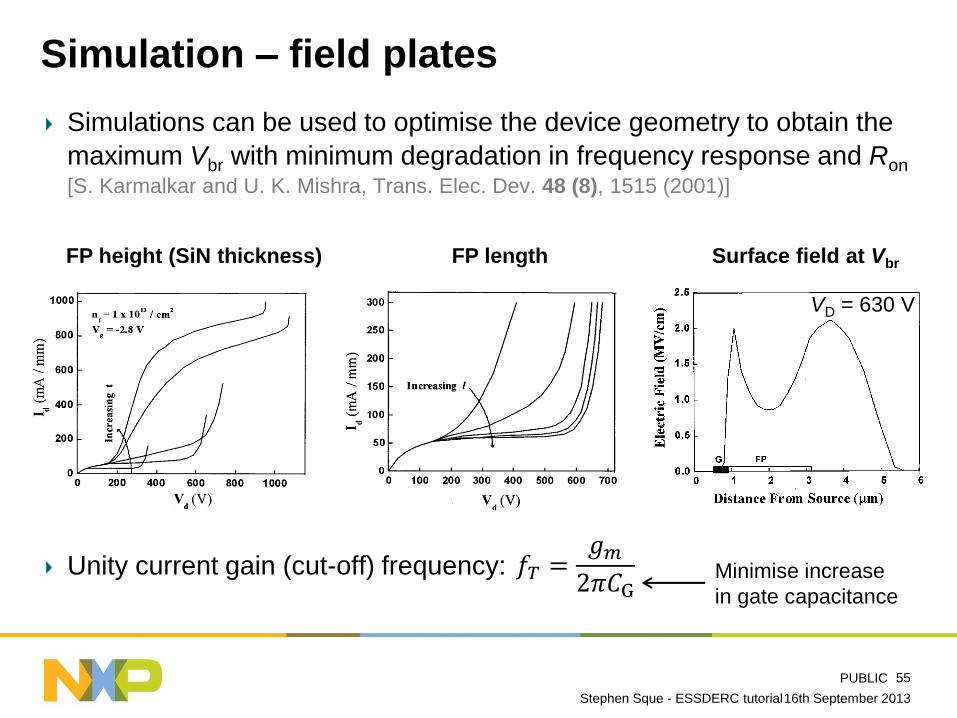
Simulation – field plates
Simulations can be used to optimise the device geometry to obtain the
maximum Vbr with minimum degradation in frequency response and Ron [S. Karmalkar and U. K. Mishra, Trans. Elec. Dev. 48 (8), 1515 (2001)]
Unity current gain (cut-off) frequency:
16th September 2013 Stephen Sque - ESSDERC tutorial
55
VD = 630 V
FP height (SiN thickness) FP length Surface field at Vbr
𝑓𝑇 =𝑔𝑚2𝜋𝐶G
Minimise increase
in gate capacitance

PUBLIC
Simulation – field plates
Making the gate-connected field plate too long can reduce Vbr
– Depending on definition of Vbr!
16th September 2013 Stephen Sque - ESSDERC tutorial
56
[H. Onodera and K. Horio, Proc. EMICC (EuMIC) 2012, 401]
PUBLIC
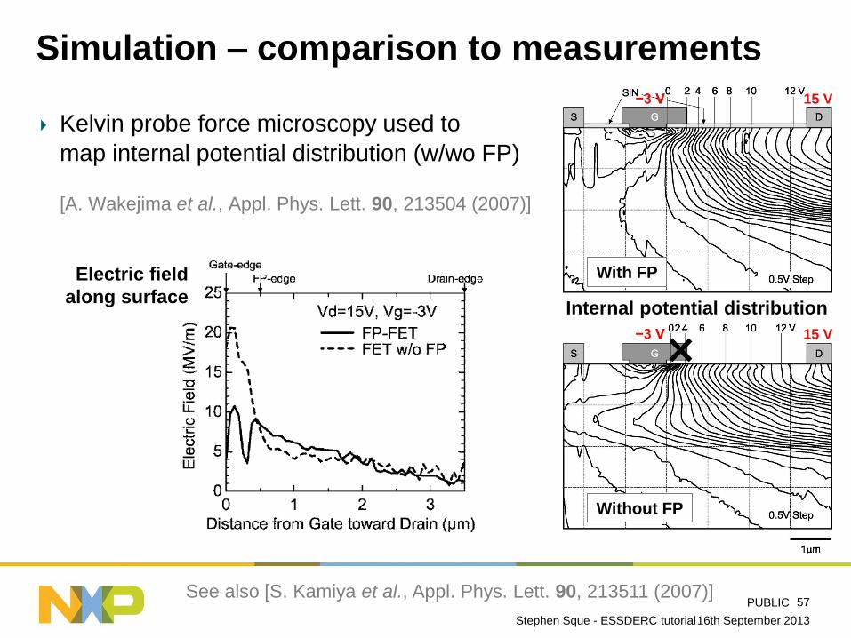
Simulation – comparison to measurements
Kelvin probe force microscopy used to
map internal potential distribution (w/wo FP)
[A. Wakejima et al., Appl. Phys. Lett. 90, 213504 (2007)]
16th September 2013 Stephen Sque - ESSDERC tutorial
57
Electric field
along surface Internal potential distribution
−3 V 15 V
−3 V 15 V
See also [S. Kamiya et al., Appl. Phys. Lett. 90, 213511 (2007)]
With FP
Without FP
PUBLIC
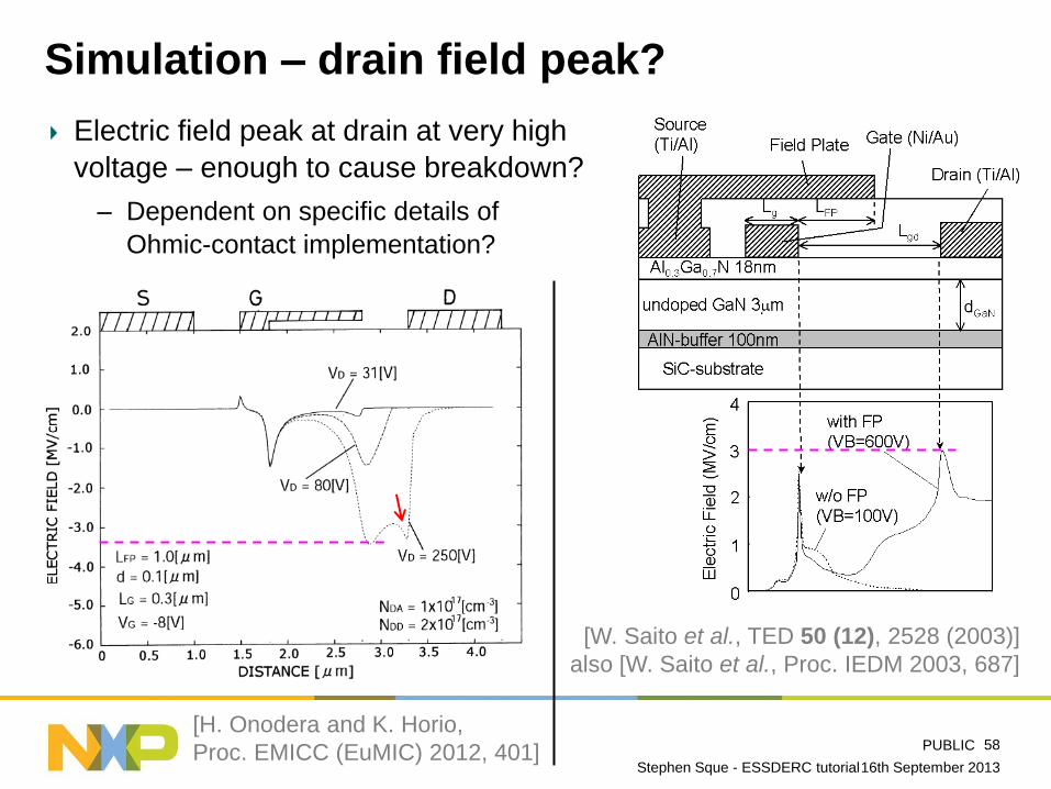
Simulation – drain field peak?
Electric field peak at drain at very high
voltage – enough to cause breakdown?
– Dependent on specific details of
Ohmic-contact implementation?
16th September 2013 Stephen Sque - ESSDERC tutorial
58
[H. Onodera and K. Horio,
Proc. EMICC (EuMIC) 2012, 401]
[W. Saito et al., TED 50 (12), 2528 (2003)]
also [W. Saito et al., Proc. IEDM 2003, 687]

PUBLIC
Simulation – impact ionisation
Improved modelling of impact ionisation
can have a significant effect on
simulated breakdown voltages
– Treat impact-ionisation parameters
as tuning parameters
16th September 2013 Stephen Sque - ESSDERC tutorial
59 [K. Kodama et al., J. Appl. Phys. 114, 044509 (2013)]
PUBLIC
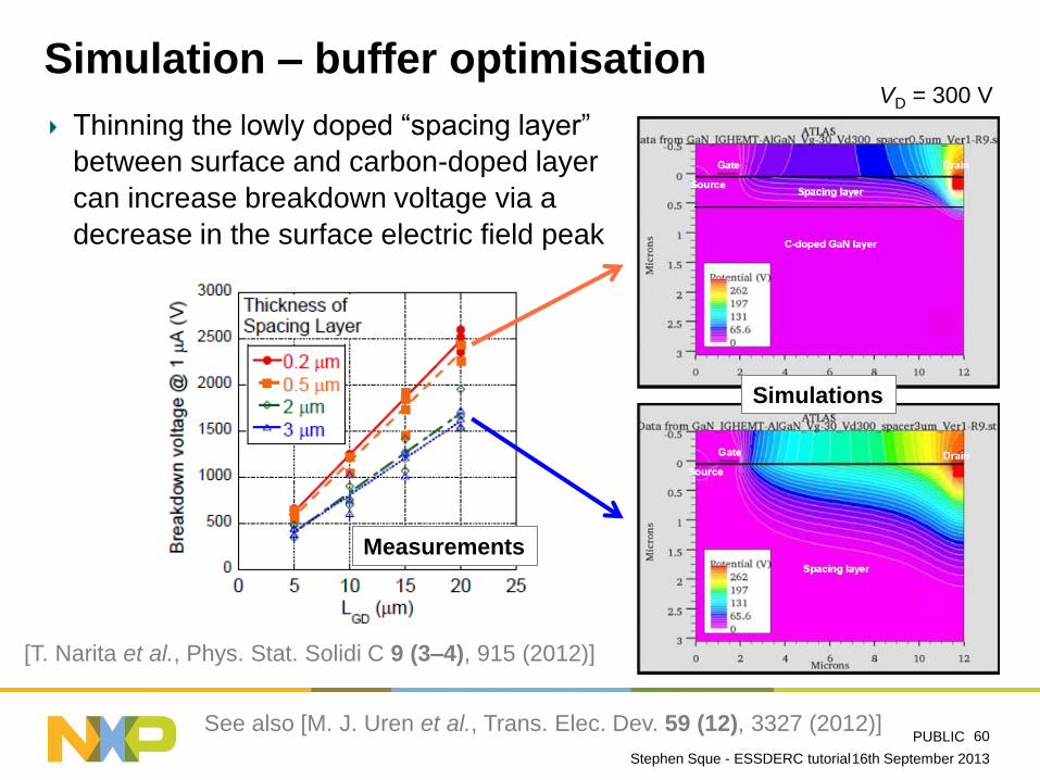
Simulation – buffer optimisation
Thinning the lowly doped “spacing layer”
between surface and carbon-doped layer
can increase breakdown voltage via a
decrease in the surface electric field peak
16th September 2013 Stephen Sque - ESSDERC tutorial
60
[T. Narita et al., Phys. Stat. Solidi C 9 (3–4), 915 (2012)]
VD = 300 V
Measurements
Simulations
See also [M. J. Uren et al., Trans. Elec. Dev. 59 (12), 3327 (2012)]

PUBLIC
Simulation – multiphysics
Thermo-electro-elastic simulations: – fully coupled thermal, mechanical,
and electrical equations
Used to investigate (for example): – The role of thermal and piezoelectric stresses on defect formation
– …and the impact on electrical characteristics
16th September 2013 Stephen Sque - ESSDERC tutorial
61
TEM [U. Chowdhury et al.,
EDL 29 (10), 1098 (2008)]
[M. G. Ancona et al., J. Appl. Phys. 111, 074504 (2012)]
[M. G. Ancona, Proc. IEDM 2012, 315]

PUBLIC
Outline
GaN and related materials
The AlGaN/GaN heterostructure
GaN wafers
GaN devices
Issues facing high-voltage GaN-HEMT development
High-voltage breakdown
GaN-HEMT device simulation
Compact modelling of GaN HEMTs
Summary and conclusion
16th September 2013 Stephen Sque - ESSDERC tutorial
62

PUBLIC
Modelling – compact models
Models for GaN devices are needed to enable application development
via circuit simulation and optimisation
Different types of compact model:
– Table-based: measured device data stored in large look-up tables
• Very fast, but extrapolation outside of measured range is treacherous,
and accurate scaling to other device dimensions is not possible
– Empirical: uses whichever mathematical functions have the right shape
• Good fits possible, but parameters are not physically meaningful,
scaling is not physical, and extrapolation is still dubious
– Physics-based: equations derived from modelling physical phenomena
• Parameters physically meaningful, scaling is physical, extrapolation reliable
• Threshold-voltage–based: physical expressions smoothed together
• Surface-potential–based: uses a single expression for all regimes,
inherent symmetry, established as the preferred approach in MOS modelling
[Gildenblat et al., J. Solid-State Circ. 39 (9), 1394 (2004)]
16th September 2013 Stephen Sque - ESSDERC tutorial
63 See also [L. Dunleavy et al., Microwave Magazine 11 (6), 82 (2010)]

PUBLIC
Modelling – empirical model
Chalmers (a.k.a. Angelov) model – An empirical model for HEMT and MESFET devices, introduced in 1992
[I. Angelov et al., Trans. Micro. Theory. Tech. 40 (12), 2258 (1992)]
– Extended in 1996 to include temperature, dispersion, and soft breakdown
[I. Angelov et al., TMTT 44 (10), 1664 (1996)]
– Widely used for (RF) GaN-HEMTs
– Modified in 2010 to make parameters more physical [T. Oishi et al., Proc. INMMIC 2010, 20 (2010)]
16th September 2013 Stephen Sque - ESSDERC tutorial
64 [I. Angelov et al., Proc. MTT 2012, 1 (2012)]
[I. Angelov et al., Proc. APMC 2006, 279]
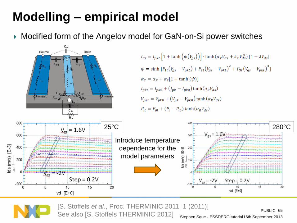
PUBLIC
Modelling – empirical model
Modified form of the Angelov model for GaN-on-Si power switches
16th September 2013 Stephen Sque - ESSDERC tutorial
65
25°C 280°C
Introduce temperature
dependence for the
model parameters
[S. Stoffels et al., Proc. THERMINIC 2011, 1 (2011)]
See also [S. Stoffels THERMINIC 2012]
PUBLIC
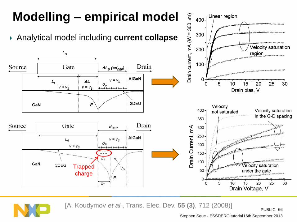
Modelling – empirical model
Analytical model including current collapse
16th September 2013 Stephen Sque - ESSDERC tutorial
66 [A. Koudymov et al., Trans. Elec. Dev. 55 (3), 712 (2008)]
Trapped
charge
PUBLIC
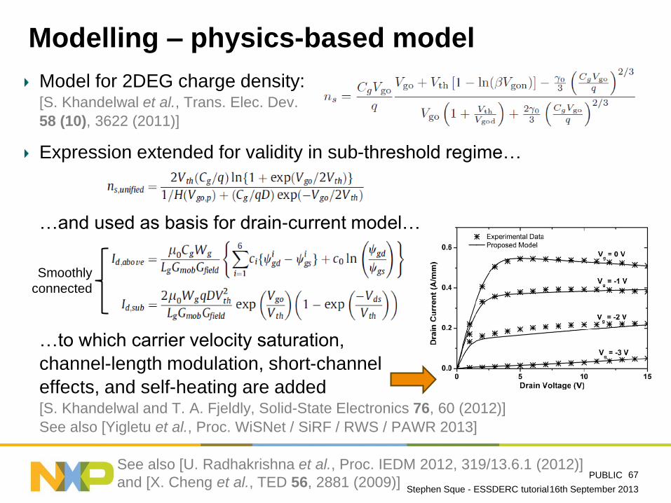
Modelling – physics-based model
Model for 2DEG charge density: [S. Khandelwal et al., Trans. Elec. Dev.
58 (10), 3622 (2011)]
Expression extended for validity in sub-threshold regime…
…and used as basis for drain-current model…
…to which carrier velocity saturation,
channel-length modulation, short-channel
effects, and self-heating are added [S. Khandelwal and T. A. Fjeldly, Solid-State Electronics 76, 60 (2012)]
See also [Yigletu et al., Proc. WiSNet / SiRF / RWS / PAWR 2013]
16th September 2013 Stephen Sque - ESSDERC tutorial
67
Smoothly
connected
See also [U. Radhakrishna et al., Proc. IEDM 2012, 319/13.6.1 (2012)]
and [X. Cheng et al., TED 56, 2881 (2009)]

PUBLIC
Modelling – physics-based model
“Zone-based” compact model based on
observations from device simulations
– Different equations derived for different
regions of the device, then smoothly joined
– Alternative to equivalent-circuit models
16th September 2013 Stephen Sque - ESSDERC tutorial
68
Simulations
Model
Output
[R. J. Trew, Proc. CSICS 2010, 1 (2010)]
[R. J. Trew et al., Proc. ICWITS 2012, 1 (2012)]
[H. Yin et al., Proc. IMS 2007, 787 and Proc. IMS 2008, 1425]
and [D. Hou et al., TED 60 (2), 639 (2013)]

PUBLIC
Modelling – surface-potential–based model
The “first surface-potential–based compact model for RF GaN HEMTs”
16th September 2013 Stephen Sque - ESSDERC tutorial
69 [D. L. John et al., Proc. IEDM 2010, 186/8.3.1 (2010)]
TCAD / physics
Model
Sub-circuit
implementation Output

PUBLIC
Modelling – surface-potential–based model
A Surface-Potential-Based Compact Model for AlGaN/GaN MODFETs
[X. Cheng and Y. Wang, Trans. Elec. Dev. 58 (2), 448 (2011)]
Analytical Modeling of Surface-Potential and Intrinsic Charges in AlGaN/GaN HEMT Devices
[S. Khandelwal et al., Trans. Elec. Dev. 59 (10), 2856 (2012)] and unpub. Trans. Elec. Dev.
16th September 2013 Stephen Sque - ESSDERC tutorial
70 See also [R. Jana and D. Jena, Proc. DRC 2012, 147 (2012)]
and [Martin / Hahe / Lucci (2012–2013)]

PUBLIC
Outline
GaN and related materials
The AlGaN/GaN heterostructure
GaN wafers
GaN devices
Issues facing high-voltage GaN-HEMT development
High-voltage breakdown
GaN-HEMT device simulation
Compact modelling of GaN HEMTs
Summary and conclusion
16th September 2013 Stephen Sque - ESSDERC tutorial
71
PUBLIC
Summary and conclusion
The material properties of GaN and AlGaN, together with the
remarkable properties of the AlGaN/GaN heterostructure,
enable the creation of high-power, high-frequency devices
Issues affecting AlGaN/GaN-based device development include:
leakage currents, current collapse (dynamic behaviour), reliability,
and sub-optimal breakdown
Device simulation can be used to explore and address these issues,
for example through buffer-composition and field-plate optimisation
Compact models for GaN HEMTs are maturing into surface-potential–
(physics-) based models with high accuracy, efficiency, and scalability (the Compact Model Council is currently choosing a standard GaN-HEMT compact model)
16th September 2013 Stephen Sque - ESSDERC tutorial
72
PUBLIC
16th September 2013
73
Acknowledgements
NXP Semiconductors: Dick Büthker, Jeroen Croon, Romain Delhougne,
Johan Donkers, Valerie Girault, Dirk Gravesteijn, Stephan Heil, Fred Hurkx,
Ponky Ivo, Dick Klaassen, Robert Lander, Twan van Lippen, Ralf van Otten,
Saurabh Pandey, Matthias Rose, Jan Šonský, Poh Cheng Tan, and
Marnix Willemsen
University of Cambridge: Giorgia Longobardi and Florin Udrea