GS66508T-EVBDB2/GS66516T-EVBDB2 GaN E-HEMT Daughter …
32
GS66508T-EVBDB2 GS66516T-EVBDB2 650V GaN E-HEMT Evaluation Board Technical Manual _____________________________________________________________________________________________________________________ GS66508T/GS66516T-EVBDB2 UG rev. 200525 © 2020 GaN Systems Inc. www.gansystems.com 1 Please refer to the Evaluation Board/Kit Important Notice on page 32 GS66508T-EVBDB2/GS66516T-EVBDB2 GaN E-HEMT Daughter Board and GS665MB-EVB Evaluation Platform Technical Manual Visit www.gansystems.com for the latest version of this technical manual. DANGER! This evaluation kit is designed for engineering evaluation in a controlled lab environment and should be handled by qualified personnel ONLY. High voltage will be exposed on the board during the test and even brief contact during operation may result in severe injury or death. Never leave the board operating unattended. After it is de-energized, always wait until all capacitors are discharged before touching the board. CAUTION This product contains parts that are susceptible to damage by electrostatic discharge (ESD). Always follow ESD prevention procedures when handling the product.
Transcript of GS66508T-EVBDB2/GS66516T-EVBDB2 GaN E-HEMT Daughter …

GS66508T-EVBDB2 GS66516T-EVBDB2
650V GaN E-HEMT Evaluation Board Technical Manual _____________________________________________________________________________________________________________________
GS66508T/GS66516T-EVBDB2 UG rev. 200525 © 2020 GaN Systems Inc. www.gansystems.com 1
Please refer to the Evaluation Board/Kit Important Notice on page 32
GS66508T-EVBDB2/GS66516T-EVBDB2 GaN E-HEMT Daughter Board and GS665MB-EVB Evaluation Platform Technical Manual
Visit www.gansystems.com for the latest version of this technical manual.
DANGER! This evaluation kit is designed for engineering evaluation in a controlled lab environment and should be handled by qualified personnel ONLY. High voltage will be exposed on the board during the test and even brief contact during operation may result in severe injury or death. Never leave the board operating unattended. After it is de-energized, always wait until all capacitors are discharged before touching the board.
CAUTION This product contains parts that are susceptible to damage by electrostatic discharge (ESD). Always follow ESD prevention procedures when handling the product.
GS66508T-EVBDB2 GS66516T-EVBDB2
650V GaN E-HEMT Evaluation Board Technical Manual _____________________________________________________________________________________________________________________
GS66508T/GS66516T-EVBDB2 UG rev. 200525 © 2020 GaN Systems Inc. www.gansystems.com 2
Please refer to the Evaluation Board/Kit Important Notice on page 32
Overview The GS665XXT-EVBDB2 daughter board evaluation kit consists of two GaN Systems 650V GaN Enhancement-mode HEMTs (E-HEMTs) and all necessary circuits including half bridge gate drivers, isolated power supplies and an optional heatsink to form a functional half bridge power stage. It allows users to easily evaluate the GaN E-HEMT performance in any half bridge-based topology, either with the universal mother board (P/N: GS665MB-EVB) or users’ own system design for quick prototyping.
Features
• Serves as a reference design and evaluation tool as well as deployment-ready solution for easy in-system evaluation.
• Vertical mount style with height of 35mm, which fits in majority of 1U design and allows evaluation of GaN E-HEMT in traditional through-hole type power supply board.
• Current shunt position for switching characterization testing • Universal form factor and footprint for all products
The daughter board and universal mother board ordering part numbers are below:
Table 1 Ordering part numbers
Part Number GaN E-HEMT P/N:
Description
GS66508T-EVBDB2 GS66508T GaN E-HEMT top side cooled 650V/30A, 50mΩ, Broadcom isolated driver ACPL-P346
GS66516T-EVBDB2 GS66516T GaN E-HEMT top side cooled 650V/60A, 25mΩ Broadcom isolated driver ACPL-P346
GS665MB-EVB GS665MB-EVB Universal 650V Mother Board
Control and Power I/Os
The daughter board GS665XXT-EVBDB2 circuit diagram is shown in Figure 1. The control logic inputs on 2x3 pin header J1 are listed below:
Table 2 Control pins
Pin Descriptipon VCC Auxillary power supply input for logic circuit and gate driver. The daughter board has 2
isolated 5V to 10V DC/DC power supplies (split +6V / -4V) for top and bottom E-HEMTs VDRV Optional 9V gate drive power input. This pin allows users to supply separate gate drive
power supply. By default VDRV is connected to VCC on the daughter board via a 0 ohm jumper FB1. If bootstrap mode is used for high side gate drive, connect VDRV to 9V
PWMH High side PWM logic input for top switch Q1. It is compatible wth 3.3V and 5V PWML Low side PWM logic input for bottom switch Q2. It is compatible wth 3.3V and 5V 0V Logic inputs and gate drive power supply ground return.

GS66508T-EVBDB2 GS66516T-EVBDB2
650V GaN E-HEMT Evaluation Board Technical Manual _____________________________________________________________________________________________________________________
GS66508T/GS66516T-EVBDB2 UG rev. 200525 © 2020 GaN Systems Inc. www.gansystems.com 3
Please refer to the Evaluation Board/Kit Important Notice on page 32
Power pins • VDC+: Input DC Bus voltage • VSW: Switching node output • VDC-: Input DC bus voltage ground return. Note that control ground 0V is isolated from VDC-.
Figure 1 GS665XXT-EVBDB2 Evaluation Board Block Diagram
GS66508T/GS66516T-EVBDB2 half bridge daughter board
Figure 2 GS66508T/GS66516T-EVBDB2 bottom side (without heatsink)
A. 2x GaN Systems 650V E-HEMT GS66508T (30A/50mΩ) or GS66516T (60A/25 mΩ). The PCB
footprints are universal and compatible for both packages B. 5V to 10V (split into +6V/-4V) isolated DC/DC gate drive power supply

GS66508T-EVBDB2 GS66516T-EVBDB2
650V GaN E-HEMT Evaluation Board Technical Manual _____________________________________________________________________________________________________________________
GS66508T/GS66516T-EVBDB2 UG rev. 200525 © 2020 GaN Systems Inc. www.gansystems.com 4
Please refer to the Evaluation Board/Kit Important Notice on page 32
Figure 3 GS66508T/GS66516T-EVBDB2 top side
C. Decoupling capacitors C4-C11 D. Isolated gate driver E. Optional current shunt position JP1. F. Test points for bottom Q2 VGS. G. Recommended probing positions for Q2 VDS. H. Holes for temperature monitoring of Q1/Q2 I. M3 mounting screw for heatsink J. (Optional) RC snubber circuit

GS66508T-EVBDB2 GS66516T-EVBDB2
650V GaN E-HEMT Evaluation Board Technical Manual _____________________________________________________________________________________________________________________
GS66508T/GS66516T-EVBDB2 UG rev. 200525 © 2020 GaN Systems Inc. www.gansystems.com 5
Please refer to the Evaluation Board/Kit Important Notice on page 32
GaN E-HEMTs
This daughter board includes two GaN Systems E-HEMTs: either two GS66508T (650V/30A, 50mΩ) or two GS66516T (650V/60A, 25mΩ) in a GaNPX® top-side cooled package. The thermal pad on top of the device is internally connected to the source. Electrical insulation will be needed for heatsink attachment. The GaNPX® T-package also features a dual symmetrical gate for easier paralleling and PCB layout.
Figure 4 Package outline of GaNPX® T Package
Gate drive power supply
• A bipolar gate drive bias with +6V and -4V for turning off is chosen for this design for more robust gate drive and better noise immunity.
• 5V to +10V isolated DC/DC converters are used for gate drive. The 10V is then splited into +6V and -4V bias by using a 6V Zener diode
• By default, the gate drive supply input VDRV is tied to VCC +5V via a 0Ω jumper (FB1). Remove FB1 if separate gate drive input voltage is to be used.
Gate driver circuit
• The half bridge evalualtion boards use two Broadcom gate drive optocoulers (ACPL-P346) to drive the GaN transistors directly. The ACPL-P346 gate driver optocoupler is used to isolate and drive the GaN transistor, operating at high DC bus voltage. It has a rail-to-rail output with maximum output current of 2.5A to provide fast switching high voltage and driving current to turn the GaN device on and off efficiently and reliably. The drive output is separated by a diode and a 10Ω gate resistor is used to limit the current for sourcing and a 2Ω gate resistor for sinking.
• The ACPL-P346 has a propagation delay of less than 110 ns and typical rise and fall times of approximately 8 ns. The very high Common Mode Rejection (CMR) of 100kV/us (min) isolates high transient noise during the high frequency operation and prevents erroneous outputs. It can provide isolation certified by UL 1577 for up to VISO 3750VRMS/min and IEC 60747-5-5 for working voltage, VIORM up to 891 VPEAK.
• The GaN E-HEMT switching speed and slew rate can be directly controlled by the gate resistors. By default the turn-on gate resistors, R6/R12, are 10Ω and turn-off gate resistosr, R7/R14, are 2Ω. The user can adjust the values of gate resistors to fine tune the turn-on and turn-off speed.
• FB2/FB3 are footprints for optional ferrite bead. By default they are populated with 0Ω jumpers. If gate oscillation is observed, it is recommended to replace them with ferrite bead with Z=10-20Ω@100MHz.

GS66508T-EVBDB2 GS66516T-EVBDB2
650V GaN E-HEMT Evaluation Board Technical Manual _____________________________________________________________________________________________________________________
GS66508T/GS66516T-EVBDB2 UG rev. 200525 © 2020 GaN Systems Inc. www.gansystems.com 6
Please refer to the Evaluation Board/Kit Important Notice on page 32
Figure 5 Gate bias and driver circuit
RC Snubber
RS1/CS1 and RS2/CS2 are place holders to allow user to experiement with the RC snubber circuit, which is not populated. At high frequency operation the power dissipation for RS1/RS2 needs to be closely watched and CS1/CS2 should be sized correctly. It is recommended to start with 33-47 pF and 10-20 Ω.
Current shunt JP1
• The board provides an optional current shunt position JP1 between the source of Q2 and power ground return. This allows drain current measurement for switching characterization test such as Eon/Eoff measurement.
• The JP1 footprint is compatible with T&M Research SDN series coaxial current shunt (recommended P/N: SDN-414-10, 2GHz B/W, 0.1Ω)
• If current shunt is not used JP1 must be shorted. JP1 affects the power loop inductance and its inductance should be kept as low as possible. Use a copper foil or jumper with low inductance.
Figure 6 Recommended probe connection with current shunt
Current Shunt
Q2 Source VDC-

GS66508T-EVBDB2 GS66516T-EVBDB2
650V GaN E-HEMT Evaluation Board Technical Manual _____________________________________________________________________________________________________________________
GS66508T/GS66516T-EVBDB2 UG rev. 200525 © 2020 GaN Systems Inc. www.gansystems.com 7
Please refer to the Evaluation Board/Kit Important Notice on page 32
CAUTION
Check JP1 before the first time use. To complete the circuit, JP1 needs to be either shorted or a current shunt must be inserted before powering up.
Measurement with current shunt
1. When measuring VSW with current shunt, ensure all channel probe grounds and current shunt BNC output case are all referenced to the source end of Q2 before the current shunt. The recommended setup of probes is shown as below.
2. The output of coaxial current shunt can be connected to oscilloscope via 50Ω termination impedance to reduce the ringing.
3. The measured current is inverted and can be scaled by using: Id=Vid/Rsense.
Figure 7 Recommended probe connection with current shunt
Thermal design
1. The GS66508T and GS66516T E-HEMTs have a thermal pad on the top side for improved heat dissipation. Instead of relying solely on the PCB for cooling, heat can be transferred to a heatsink directly from the top of the E-HEMT, reducing the total thermal resistance.
2. A heatsink can be mounted to the board using a M3 screw with lock washer and nylon insulated bushing. A Thermal Interface Material (TIM) is needed to provide electrical insulation and conformance to the thermal pad surface. The daughter board evaluation kit supplies with a 35x35mm heatsink with M3 tapped hole. Other heatsinks can also be used to fit users’ system design.
3. Care should be taken during the assembly of the heatsink to avoid PCB bending and mechanical stress to the GaN E-HEMT. We recommend to limit the torque of M3 mounting screw to <1 in-lb (0.1Nm) for GS66508T and <2 in-lb (0.2Nm) for GS66516T, which translates to about ~50psi pressure on each device.
VGL
VSL
VSW
BNC case
To oscilloscope probe input (use 50Ω termination)
BNC tip
VDSVGS
ID

GS66508T-EVBDB2 GS66516T-EVBDB2
650V GaN E-HEMT Evaluation Board Technical Manual _____________________________________________________________________________________________________________________
GS66508T/GS66516T-EVBDB2 UG rev. 200525 © 2020 GaN Systems Inc. www.gansystems.com 8
Please refer to the Evaluation Board/Kit Important Notice on page 32
WARNING
Over-torquing the heatsink may create excess mechanical stress and could result in device failure. Always follow the maximum torque spec and attach the heatsink carefully to avoid any PCB bending or high pressing force on the devices.
4. The E-HEMT case temperature, can be monitored using an IR camera or a thermocouple through
two drilled holes from the top side as shown below:
Figure 8 Location for case temperature monitoring
CAUTION There is no on-board over-temperature protection. Monitor the E-HEMT temperature closely during the test. Never operate the board with device temperature exceeding TJ_MAX (150°C)
5. The TIM we use on this assembly is Berguist® SilPad 1500ST, the measured total thermal
resistance can be found in Figure 9. Compared to a bottom-cooled design, the top-side cooled package eliminates the PCB thermal resistance and significantly improve the thermal performance. Thermal grease is typically not needed on the assembly. If thermal grease is applied, use non-conductive and non-capacitive type thermal grease.
6. Forced air cooling is recommended for power testing.

GS66508T-EVBDB2 GS66516T-EVBDB2
650V GaN E-HEMT Evaluation Board Technical Manual _____________________________________________________________________________________________________________________
GS66508T/GS66516T-EVBDB2 UG rev. 200525 © 2020 GaN Systems Inc. www.gansystems.com 9
Please refer to the Evaluation Board/Kit Important Notice on page 32
Figure 9 Evaluation board thermal resistance comparison
Figure 10: The daughter board assembly with heatsink attached
GaNPX T GaNPX TFR4 PCB
Heatsink
M3 Screw
Lock WashterInsulated bushing
TIM

GS66508T-EVBDB2 GS66516T-EVBDB2
650V GaN E-HEMT Evaluation Board Technical Manual _____________________________________________________________________________________________________________________
GS66508T/GS66516T-EVBDB2 UG rev. 200525 © 2020 GaN Systems Inc. www.gansystems.com 10
Please refer to the Evaluation Board/Kit Important Notice on page 32
Using GS665XXT-EVBDB2 with universal mother board GS665MB-EVB
Figure 11: 650V universal mother board GS665MB-EVB
GaN Systems provides a universal 650V mother board (ordering part number: GS665MB-EVB, sold separately) that can be used as the basic evaluation platform for all the daughter boards.
The universal 650V mother board evaluation kit includes following items: 1. Mother board GS665MB-EVB 2. 12VDC Fan
ENABLE
Although connector J5, pin 2, on the universal motherboard indicates the presence of ENABLE, this feature is not available on the GS66508T-EVBDB2 and GS66516T-EVBDB2 daughterboards.
12V input
The board can be powered by 9-12V on J1. On-board voltage regulator creates to 5V for daughter board and control logic circuits. J3 is used for external 12VDC fan.

GS66508T-EVBDB2 GS66516T-EVBDB2
650V GaN E-HEMT Evaluation Board Technical Manual _____________________________________________________________________________________________________________________
GS66508T/GS66516T-EVBDB2 UG rev. 200525 © 2020 GaN Systems Inc. www.gansystems.com 11
Please refer to the Evaluation Board/Kit Important Notice on page 32
PWM control circuit
Figure 12 PWM control input and dead time circuit
Figure 13 On board dead time generatrion circuit
Although connector J5, pin 2, on the universal motherboard indicates the presence of ENABLE, this feature is not available on the GS66508T-EVBDB2 and GS66516T-EVBDB2 daughterboards.
The top and bottom switches PWM inputs can be individually controlled by two jumpers J4 and J6. Users can choose between a pair of complementary on-board internal PWM signals (non-inverted and inverted, controlled by J7 input) with dead time or external high/low side drive signals from J5 (users’ own control board).
An on-board dead time generation circuit is included on the mother board. Dead time is controlled
0V
D1 PMEG2005EB
SOD523
R6
1K00
TR12K C11100pF
0V
R5
1K00
C10
1uF
C9
0.1uF
+5V
J7112538
1
2345
R4100RR1206
R2100RR1206
U2A
74VHC132
31
2
147
0V
R1
49R90V
D2 PMEG2005EB
SOD523
TR22K
C12100pF
0V
U2B
74VHC132
4
56
U2C
74VHC132
9
108
U2D
74VHC132
12
1311
TP7
TP8
DNP
DNP
PWM OUTPUT
INVERTED PWM OUTPUT
R3
49R9
DNPDNP
R7
49R9

GS66508T-EVBDB2 GS66516T-EVBDB2
650V GaN E-HEMT Evaluation Board Technical Manual _____________________________________________________________________________________________________________________
GS66508T/GS66516T-EVBDB2 UG rev. 200525 © 2020 GaN Systems Inc. www.gansystems.com 12
Please refer to the Evaluation Board/Kit Important Notice on page 32
by two RC delay circuits, R6/C12 and R5/C11. The default dead time is set to about 100ns. Additionally two potentiometers locations are provided (TR1/TR2, not included) to allow fine adjustment of the dead time if needed.
WARNING ALWAYS double check the jumper setting and PWM gate drive signals before applying power. Incorrect PWM inputs or jumper settings may cause device failures
Test points
Test points are designed in groups/pairs to facilitate probing:
Test points Name Description TP1/TP2 +5V/0V 5V bias power TP7/TP8 PWMIN/0V PWM input signal from J7 TP4/TP3/TP13 PWMH/PWML/0V High/low side gate signals to daughter board TP9/TP10 VDC+/VDC- DC bus voltage TP11/TP12 VOUT/VDC- Output voltage TP6/TP5 VSW/VDC- Switching node output voltage (for HV oscilloscope probe)
Power connections
CON1-CON7 mounting pads are designed to be compatible with following mounting terminals: • #10-32 Screw mount, • Banana Jack PCB mount (Keystone P/N: 575-4), or • PC Mount Screw Terminal (Keystone P/N: 8191)
Output passives (L and C14)
An external power inductor (not included) can be connected between VSW (CON1) and VOUT (CON4/5) or VDC+ (CON2/3) for double pulse test. Users can choose the inductor size to meet their test requirements. It is generally recommended to select a power inductor with low inter-winding capacitance to obtain best switching performance. For the double pulse testing we use 2x 60uH/40A inductor (CWS, P/N: HF467-600M-40AV) in series. C14 is designed to accommodate a film capacitor as output filter.
GS66508T-EVBDB2 GS66516T-EVBDB2
650V GaN E-HEMT Evaluation Board Technical Manual _____________________________________________________________________________________________________________________
GS66508T/GS66516T-EVBDB2 UG rev. 200525 © 2020 GaN Systems Inc. www.gansystems.com 13
Please refer to the Evaluation Board/Kit Important Notice on page 32
Using GS665XXT-EVBDB2 in system The daughter board allows users to easily evaluate the GaN performance in their own systems. Refer to the footprint drawing of GS665XXT-EVBDB2 as shown below:
Figure 14 Recommended footprint drawing of daughter board GS665XXT-EVBDB2
1 3 5
2 4 6
78 9
1. All units are in mm.2. Pin 1-6: Dia. 1mm3. Pin 7-9: 1.91mm (75mil) mounting hole for Mill-max Receptacle P/N: 0312-0-15-15-34-27-10-0.

GS66508T-EVBDB2 GS66516T-EVBDB2
650V GaN E-HEMT Evaluation Board Technical Manual _____________________________________________________________________________________________________________________
GS66508T/GS66516T-EVBDB2 UG rev. 200525 © 2020 GaN Systems Inc. www.gansystems.com 14
Please refer to the Evaluation Board/Kit Important Notice on page 32
Double pulse test mode
CON1
Q1
CON2
Q2
VDC-
CON4
CON3
LOUT
400V DC
+
VDC+
CON7CON6
VSWCON5
+5V
0V
PWM INPUT
(J7)
VDS
IL
ISW
VGL
+6V
0VVDS
VGL
IL
t0 t1 t2 t3TON1
Figure 15 Double pulse test setup
Double pulse test allows easy evaluation of device switching performance at high voltage/current without the need of actually running at high power. It can also be used for switching loss (Eon/Eoff) measurement and other switching characterization parameter test.
The circuit configuration and operating principle can be found in Figure 14: 1. The output inductor is connected to the VDC+. 2. At t0 when Q2 is switched on, the inductor current starts to ramp up until t1. The period of first
pulse Ton1 defines the switching current ISW = (VDS*TON1) / L. 3. t1-t2 is the free wheeling period when the inductor current IL forces Q1 to conduct in reverse. 4. t1 (turn-off) and t2 (turn-on) are of interest for this test as they are the hard switching trasients for
the half bridge circuit when Q2 is under high switching stress. 5. The second pulse t2-t3 is kept short to limit the peak inductor current at t3.
The double pulse signal can be generated using programmable signal generaotor or microcontroller/DSP board. As this test involves high switching stress and high current, it is recommended to set the double pulse test gate signal as single trigger mode or use long repetition period (for example >50-100ms) to void excess stress to the switches. Q1 can be kept off during the test or driven synchronously (J4 set to OFF or INT_INV) and Q2 is set to INT (or EXT position if PWM signal is from J5).
WARNING Limit the maximum switching test current to 30A for GS66508T (60A for GS66516T) and ensure maximum drain voltage, including ringing, is kept below 650V for pulse testing. Exceeding this limit may cause damage to the devices.

GS66508T-EVBDB2 GS66516T-EVBDB2
650V GaN E-HEMT Evaluation Board Technical Manual _____________________________________________________________________________________________________________________
GS66508T/GS66516T-EVBDB2 UG rev. 200525 © 2020 GaN Systems Inc. www.gansystems.com 15
Please refer to the Evaluation Board/Kit Important Notice on page 32
Buck/Standard half bridge mode
CON1
Q1
CON2
Q2
VDC-
CON4
CON3
LOUT
400V DC
+
VDC+
CON7
CON6
VSWCON5
COUT RLoad
This standard half bridge configuration can be used in the following circuits :
• Synchronous Buck DC/DC • Single phase half bridge inverter • ZVS half bridge LLC • Phase leg for full bridge DC/DC or • Phase leg for a 3-phase motor drive
Jumper setting:
• J4 (Q1): INT • J6 (Q2): INT_INV
Boost mode
CON1
Q1
CON2
Q2
VDC-
CON4
CON3LIN
VDC+
CON7CON6
VSWCON5
INPUT
VIN
When the output becomes the input and the load is attached between VDC+ and VDC-, the board is converted into a boost mode circuit and can be used for:
• Synchronous Boost DC/DC • Totem pole bridgeless PFC
Jumper setting:
• J4 (Q1): INT_INV • J6 (Q2): INT

GS66508T-EVBDB2 GS66516T-EVBDB2
650V GaN E-HEMT Evaluation Board Technical Manual _____________________________________________________________________________________________________________________
GS66508T/GS66516T-EVBDB2 UG rev. 200525 © 2020 GaN Systems Inc. www.gansystems.com 16
Please refer to the Evaluation Board/Kit Important Notice on page 32
Quick Start procedure – Double pulse test Follow the instructions below to quickly get started with your evaluation of GaN E-HEMT. Equipment and components you will need:
• Four-channel oscilloscope with 500MHz bandwidth or higher • high bandwidth (500MHz or higher) passive probe • high bandwidth (500MHz) high voltage probe (>600V) • AC/DC current probe for inductor current measurement • 12V DC power supply • Signal generator capable of creating testing pulses • High voltage power supply (0-400VDC) with current limit. • External power inductor (recommend toroid inductor 50-200uH)
1. Check the JP1 on daughter board GS665XXT-EVBDB2. Use a copper foil and solder to short JP1. 2. Install GS665XXT-EVBDB2 on the mother board. Press all the way down until you feel a click.
Connect probe between VGL and VSL for gate voltage measurement. 3. Set up the mother board:
a. Connect 12VDC bias supply to J1. b. Connect PWM input gate signal (0-5V) to J7. If it is generated from a signal generator ensure
the output mode is high-Z mode. c. Set J4 to OFF position and J7 to INT. d. Set High voltage (HV) DC supply voltage to 0V and ensure the output is OFF. Connect HV
supply to CON2 and CON6. e. Use HV probe between TP6 and TP5 for Vds measurement. f. Connect external inductor between CON1 and CON3. Use current probe to measure inductor
current IL. 4. Set up and check PWM gate signal:
a. Turn-on 12VDC power. b. Check the 2 LEDs on the daughter board. They should be turned on indicating the isolated
9V is present. c. Set up signal generator to create the waveforms as shown in Figure 14. Use equation ISW =
(VDS*TON1) / L to calculate the pulse width of the first pulse and ensure the Isw_max is ≤30A at 400VDC.
d. Set the operation mode to either single trigger or Burst mode with repetition period of 100ms. e. Turn on the PWM output and check on the oscilloscope to make sure the VGL waveform is
present and matches the PWM input. 5. Power-on:
a. Turn on the output of the HV supply. Start with low voltage and slowly ramp the voltage up until it reaches 400VDC. During the ramping period closely observe the the voltage and current waveforms on the oscilloscope.
6. Power-off: a. After the test is complete, slowly ramp down the HV supply voltage to 0V and turn off the
output. Then turn off the 12V bias supply and signal generator output.

GS66508T-EVBDB2 GS66516T-EVBDB2
650V GaN E-HEMT Evaluation Board Technical Manual _____________________________________________________________________________________________________________________
GS66508T/GS66516T-EVBDB2 UG rev. 200525 © 2020 GaN Systems Inc. www.gansystems.com 17
Please refer to the Evaluation Board/Kit Important Notice on page 32
Figure 16 Double pulse test setup example

GS66508T-EVBDB2 GS66516T-EVBDB2
650V GaN E-HEMT Evaluation Board Technical Manual _____________________________________________________________________________________________________________________
GS66508T/GS66516T-EVBDB2 UG rev. 200525 © 2020 GaN Systems Inc. www.gansystems.com 18
Please refer to the Evaluation Board/Kit Important Notice on page 32
Test results
Double Pulse test (VDS=400V, IMAX = 30A, L=120uH, RG(ON)=10Ω, RG(OFF)=2Ω, VGS=+6/-4V)
Figure 17 400V/30A double pulse test waveform (GS66508T)
Figure 17 shows the hard switching on waveforms at 400V/30A. A Vds dip can be seen due to the rising drain current (dI/dt in the power loop ΔV=LpxdI/dt, where Lp is the total power loop inductance). After the drain current reaches the inductor current, the Vds starts to fall. The Vgs undershoot spike is caused by the miller feedback via Cgd under negative dv/dt.
Due to the low gate charge and small RG(OFF) , GaN E-HEMT gate has limited control on the turn-off dV/dt. Instead the Vds rise time is determined by how fast the turn-off current charges switching node capacitance (Coss).
The low Coss of GaN E-HEMT and low parasitic inductance of GaNPX® package together with optimized PCB layout, enables a fast and clean turn-off Vds waveform with only 50V the turn-off Vds overshoot at dV/dt > 100V/ns. The measured rise time is 3.9ns at 400V and 30A hard turn-off.

GS66508T-EVBDB2 GS66516T-EVBDB2
650V GaN E-HEMT Evaluation Board Technical Manual _____________________________________________________________________________________________________________________
GS66508T/GS66516T-EVBDB2 UG rev. 200525 © 2020 GaN Systems Inc. www.gansystems.com 19
Please refer to the Evaluation Board/Kit Important Notice on page 32
a) Hard switching turn-on 400V/30A b) Hard switching turn-off 400V/30A
Figure 18 Double pulse test switching transient waveforms (GS66508T)
Switching Loss energy (Eon/Eoff) measurement
A T&M search coaxial current shunt (SDN-414-10, 0.1Ω) is installed for switching loss measurement as shown below.
Figure 19 Eon/Eoff measurement probe connection with current shunt

GS66508T-EVBDB2 GS66516T-EVBDB2
650V GaN E-HEMT Evaluation Board Technical Manual _____________________________________________________________________________________________________________________
GS66508T/GS66516T-EVBDB2 UG rev. 200525 © 2020 GaN Systems Inc. www.gansystems.com 20
Please refer to the Evaluation Board/Kit Important Notice on page 32
Figure 20 Eon/Eoff measurement and test bench setup
The switching energy can be calculated from the measured switching waveform Psw = Vds*Id. The integral of the Psw during switching period is the measured switching loss. The channel deskewing is critical for measurement accurary. It is recommended to manually deskew Id against Vds as shown in Figure 21. The drain current spike is caused by charging the high side switch Coss (Qoss loss).
Figure 21 Turn-on switching loss measurement (Eon=98uJ, 400V/30A, TJ=25°C)

GS66508T-EVBDB2 GS66516T-EVBDB2
650V GaN E-HEMT Evaluation Board Technical Manual _____________________________________________________________________________________________________________________
GS66508T/GS66516T-EVBDB2 UG rev. 200525 © 2020 GaN Systems Inc. www.gansystems.com 21
Please refer to the Evaluation Board/Kit Important Notice on page 32
Figure 22 Turn-off switching loss measurement (Eoff=18uJ, 400V/30A, TJ=25°C)
The switching loss measurements with drain current from 0 to 30A for GS66508T or up to 60A for GS66516T can be found in Figure 23. The turn-on loss dominates the overall hard switching loss. Eon at 0A is the Qoss loss caused by the Coss at high side switch.
Figure 23 GS66508T Switching Loss Measurement (VDS = 400V, TJ=25°C)

GS66508T-EVBDB2 GS66516T-EVBDB2
650V GaN E-HEMT Evaluation Board Technical Manual _____________________________________________________________________________________________________________________
GS66508T/GS66516T-EVBDB2 UG rev. 200525 © 2020 GaN Systems Inc. www.gansystems.com 22
Please refer to the Evaluation Board/Kit Important Notice on page 32
Figure 24 GS66516T Switching Loss Measurement (VDS = 400V, TJ=25°C)
Synchronous Buck Test (L=120uH, VIN=400V, VOUT=200V, D=50%, FSW=100 kHz, POUT =0-2.4kW)
To test the efficiency of GaN transistor in hard switching operation, the board is connected as DC-DC converter in synchronous buck configuration. The converter is operated at high frequency 100 kHz. A very high conversion efficiency of more than 98.4% is achieved using 650V E-HEMT GS66508T (30A/50mΩ) and GS66516T (60A/25mΩ) transistor and gate drive optocoupler, ACPL-P346 at 100 kHz.
Figure 25 Synchronous Buck Efficiency and thermal measurement

GS66508T-EVBDB2 GS66516T-EVBDB2
650V GaN E-HEMT Evaluation Board Technical Manual _____________________________________________________________________________________________________________________
GS66508T/GS66516T-EVBDB2 UG rev. 200525 © 2020 GaN Systems Inc. www.gansystems.com 23
Please refer to the Evaluation Board/Kit Important Notice on page 32
Figure 26 Thermal image (GS66508T, Pout=1kW)
GS66508T-EVBDB2 GS66516T-EVBDB2
650V GaN E-HEMT Evaluation Board Technical Manual _____________________________________________________________________________________________________________________
GS66508T/GS66516T-EVBDB2 UG rev. 200525 © 2020 GaN Systems Inc. www.gansystems.com 24
Please refer to the Evaluation Board/Kit Important Notice on page 32
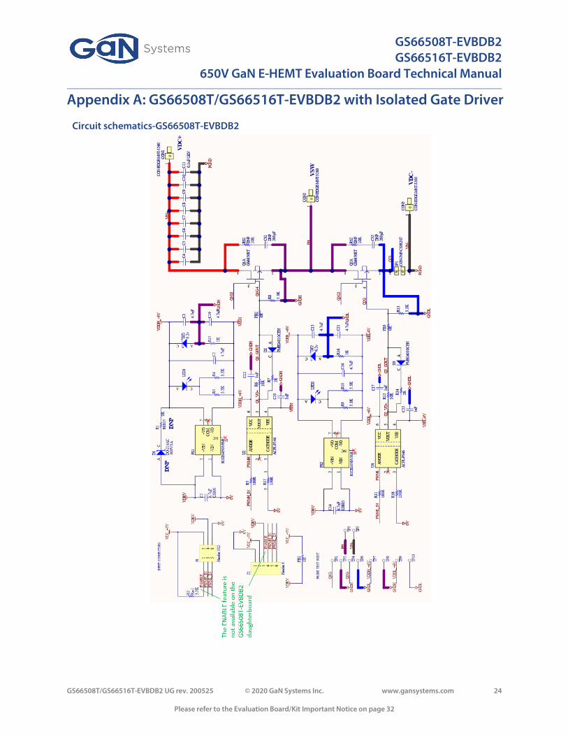
Appendix A: GS66508T/GS66516T-EVBDB2 with Isolated Gate Driver
Circuit schematics-GS66508T-EVBDB2

GS66508T-EVBDB2 GS66516T-EVBDB2
650V GaN E-HEMT Evaluation Board Technical Manual _____________________________________________________________________________________________________________________
GS66508T/GS66516T-EVBDB2 UG rev. 200525 © 2020 GaN Systems Inc. www.gansystems.com 25
Please refer to the Evaluation Board/Kit Important Notice on page 32
Circuit schematics-GS66516T-EVBDB2

GS66508T-EVBDB2 GS66516T-EVBDB2
650V GaN E-HEMT Evaluation Board Technical Manual _____________________________________________________________________________________________________________________
GS66508T/GS66516T-EVBDB2 UG rev. 200525 © 2020 GaN Systems Inc. www.gansystems.com 26
Please refer to the Evaluation Board/Kit Important Notice on page 32
Assembly Drawing (Top)
Assembly Drawing (Bottom)

GS66508T-EVBDB2 GS66516T-EVBDB2
650V GaN E-HEMT Evaluation Board Technical Manual _____________________________________________________________________________________________________________________
GS66508T/GS66516T-EVBDB2 UG rev. 200525 © 2020 GaN Systems Inc. www.gansystems.com 27
Please refer to the Evaluation Board/Kit Important Notice on page 32
PCB layout
Top Layer
Mid Layer 1
Mid Layer 2
Bottom Layer

GS66508T-EVBDB2 GS66516T-EVBDB2
650V GaN E-HEMT Evaluation Board Technical Manual _____________________________________________________________________________________________________________________
GS66508T/GS66516T-EVBDB2 UG rev. 200525 © 2020 GaN Systems Inc. www.gansystems.com 28
Please refer to the Evaluation Board/Kit Important Notice on page 32
Bill of Materials
S.NO Designator Value Description Manufacturer Part number Qty Remarks1 PCB PCB bare 4-layer 2oz Cu. 12 CON1,CON2,CON3 CON-EDGE-MNT-3260 CONN PC PIN EDGE MNT Mill-Max 3620-2-32-15-00-00-08-0 33 CS1, CS2 CAP, CER, 200pF, 630V, 1206 KEMET C1206C201FBGACTU 0 No Mount
4 C1,C2,C3,C14,C15,C16,C19,C21 4.7uF CAP, CER, 4.7UF, 25V, +/-10%, X7R, 0805 TDKC2012X5R1E475K125AB /MC0805X475K250CT 8
5 C4,C5,C6,C7,C8,C9,C10,C11 0.1uF 1kV CAP, CER, 0.1UF,1KV, +/-10%, X7R, 1812 KEMETC1812C104KDRACTU /C1812V104KDRACTU 8
6 C12,C17,C20,C22 1uF CAP, CER, 1UF, 25V, +/-10%, X7R, 0603 KEMETC0603C105K3RACTU /TMK107B7105KA-T 4
7 DZ1,DZ2 6.2V zener DIODE ZENER 6.2V 200MW SOD323 VishayBZX384C6V2-E3-08 /BZX384-C6V2 2
8 D1 600V 1A DIODE ULTRAFAST 600V 1A SMA Fairchild ES1J 0 No Mount
9 FB1,FB2,FB3 0R RES, 0R JUMPER, 1%, 0603 YageoRC0603FR-070RL/MC0603SAF0000T5E 3
10 JP1 CON-JMP-CSHUNT CURRENT SHUNT JUMPER 0 No Mount
11 J1 CON-HDR-2X3 CONN 3PIN DUAL ROW, 0.1" PITCH, R/A SAMTEC TSW-103-08-G-D-RA 112 J2 CON-6POS 0 No Mount13 LED1, LED2 LED-SMD-0603 LED, GREEN, SMD 0603 LITEON LTST-C191KGKT 214 PS1, PS2 R1DX-0505/H-R ISO. DC/DC 5-10V, 1W RECOM 215 Q1A, Q2A GS66508T GaN E-HEMT 650V/30A TOP COOL GaN Systems GS66508T 216 Q1B, Q2B GS66516T GaN E-HEMT 650V/60A TOP COOL GaN Systems GS66516T 217 RS1, RS2 10R RES, 10R, 1%, 1206 generic 0 No Mount18 R1 0R RES, 0R, 1%, 0805 generic generic 0 No Mount19 R2,R3,R4,R8,R9,R10,R13 3K3 RES, 3.3K, 1%,1/10W, 0603 Multicomp MCWR06X3301FTL 720 R6,R12 10R RES, 10R, 1%,1/10W, 0603 Bourns CR0603-FX-10R0ELF 221 R5,R11 180R RES, 180R, 1%,1/10W, 0603 Walsin WR06X1800FTL 222 R7,R14 2R RES, 2R, 1%,1/10W, 0603 Walsin WR06W2R00FTL 223 R15,R16 1K0 RES, 1K, 1%,1/10W, 0603 Yageo RC0603FR-101KL 224 R17,R18 130R RES, 130R, 1%,1/10W, 0603 Yageo RC0603FR-07130RL 225 TP1,TP2,TP3,TP4,TP5,TP6 CON-TP-1POS Probe test point 0 No Mount26 TP7,TP8,TP9,TP10 CON-TP-1POS Probe test point 0 No Mount27 U2,U4 ACPL-P346 Optocoupler Broadcom ACPL-P346-000E 2
28 D2, D3 PMEG4010CEH DIODE PMEG4010CEH SBD SOD123F NXPPMEG4010CEH /PMEG4010EH 2
29 heatsink, 35x35mmx25.4mm, customized Shenzhen Mingzhi PY16-020-1 1
30 81.58.336
M3 screw w/ insulated sleeve( Machine Screw, Spring Washer, M3, 8 mm, Steel, Zinc, Pan Head Pozidriv) ETTINGER 81.58.336 1
31 WS0330A Washer shoulder M3 NYLON Essentra WS0330A 132 Electrically insulated Thermal pad Bergquist SILPAD 1500ST 1
63

GS66508T-EVBDB2 GS66516T-EVBDB2
650V GaN E-HEMT Evaluation Board Technical Manual _____________________________________________________________________________________________________________________
GS66508T/GS66516T-EVBDB2 UG rev. 200525 © 2020 GaN Systems Inc. www.gansystems.com 29
Please refer to the Evaluation Board/Kit Important Notice on page 32
Appendix B - GS665MB-EVB – 650V Universal Motheboard
Circuit schematics

GS66508T-EVBDB2 GS66516T-EVBDB2
650V GaN E-HEMT Evaluation Board Technical Manual _____________________________________________________________________________________________________________________
GS66508T/GS66516T-EVBDB2 UG rev. 200525 © 2020 GaN Systems Inc. www.gansystems.com 30
Please refer to the Evaluation Board/Kit Important Notice on page 32
Assembly drawing
Assembly Top
Assembly Bottom

GS66508T-EVBDB2 GS66516T-EVBDB2
650V GaN E-HEMT Evaluation Board Technical Manual _____________________________________________________________________________________________________________________
GS66508T/GS66516T-EVBDB2 UG rev. 200525 © 2020 GaN Systems Inc. www.gansystems.com 31
Please refer to the Evaluation Board/Kit Important Notice on page 32
Bill of Materials
GAN
SYS
TEM
S 65
0V G
AN U
NIV
ERSA
L M
OTH
ER B
OAT
RD
BO
ARD
P/N
:G
S665
EVB
MB
Rev
isio
nB
1La
st U
pdat
e6/
30/2
016
Qua
ntity
Ref
eren
ceD
escr
iptio
nVa
lue
Man
ufac
ture
rPa
rt nu
mbe
rAs
sem
bly
Not
e 1
PC
BP
CB
bar
e 2-
laye
r 2oz
Cu.
17
CO
N1,
CO
N2,
CO
N3,
CO
N4,
CO
N5,
CO
N6,
CO
N7
TE
RM
INA
L S
CR
EW
VE
RTI
CA
L P
C M
NT
CO
N-1
0-32
-SC
RW
MN
TK
EYS
TON
E81
91D
O N
OT
INS
TALL
21
C1
CA
P A
LUM
220
UF
20%
25V
SM
D
220u
F 25
VP
anas
onic
EE
E-F
K1E
221P
31
C2,
C10
GE
NE
RIC
1U
F/25
V, 1
0% X
7R S
MD
060
31u
FTA
IYO
YU
DE
NTM
K10
7B71
05K
A-T
42
C3,
C4
GE
NE
RIC
10U
F/25
V, 1
0% S
MD
080
510
uFTA
IYO
YU
DE
NTM
K21
2BB
J106
KG
-T5
4C
5,C
6,C
7,C
8G
EN
ER
IC 0
.1uF
/100
0V, S
MD
181
20.
1uF
1kV
KE
ME
TC
1812
C10
4KD
RA
C78
006
1C
9G
EN
ER
IC 0
.1U
F/25
V, 1
0% X
7R S
MD
060
30.
1uF
TAIY
O Y
UD
EN
TMJ1
07B
B71
04K
AH
T7
2C
11,C
12G
EN
ER
IC 1
00P
F/25
V 5
% N
P0
SM
D 0
603
100p
FK
EM
ET
C06
03C
101J
3GA
CTU
81
C13
,C14
CA
P F
ILM
10U
F/60
0VD
C 5
%, 2
7.5M
M L
EA
D
SP
AC
ING
10uF
700
VK
EM
ET
C4A
EH
BU
5100
A11
JD
O N
OT
INS
TALL
C14
92
D1,
D2
DIO
DE
SC
HO
TTK
Y 20
V 5
00M
A S
OD
523
PM
EG
2005
EB
NX
PP
ME
G20
05E
B,1
1510
1J1
TER
M B
LOC
K H
DR
2P
OS
R/A
5.0
8MM
CO
N-T
ER
M-B
LK-2
PO
S-R
ATE
CO
NN
EC
TIV
ITY
7966
38-2
111
J1-P
LUG
TER
M B
LOC
K B
LUG
2P
OS
5.0
8MM
TE C
ON
NE
CTI
VIT
Y79
6634
-212
1J2
CO
NN
RC
PT
6PO
S .1
00 D
BL
STR
PC
BC
ON
-RC
PT-
2X3-
BO
TH
AR
WIN
M20
-785
0342
MO
UN
T FR
OM
BO
TTO
M S
IDE
131
J3C
ON
-2P
OS
CO
NN
EC
TOR
FO
R 1
2V F
AN
, DO
NO
T IN
STA
LL14
2J4
,J6
CO
NN
HE
AD
ER
8P
OS
DU
AL
VE
RT
PC
B
CO
N-J
MP
-4P
OS
HA
RW
INM
20-9
9804
4515
1J5
CO
NN
8-P
OS
, DU
AL
RO
W 2
.54M
MC
ON
-HD
R-4
X2
AM
PH
EN
OL
7586
9-13
2LF
161
J7C
ON
N B
NC
JA
CK
STR
50
OH
M P
CB
1125
38A
MP
HE
NO
L11
2538
173
J8,J
9,J1
0C
ON
N R
EC
EP
T P
IN .0
32-.0
46" .
075"
CO
N-R
CP
T-E
DG
EM
NT
MIL
LMA
X03
12-0
-15-
15-3
4-27
-10-
0M
ATI
NG
SO
CK
ET
FOR
MIL
LMA
X
ED
GE
MN
T P
IN
183
R1,
R3,
R7
gene
ric 1
% s
md
0603
49R
9V
ISH
AY
DA
LEC
RC
W06
0349
R9F
KE
A19
2R
2,R
4ge
neric
1%
sm
d 12
0610
0RD
O N
OT
INS
TALL
202
R5,
R6
gene
ric 1
% s
nd 0
603
1K00
VIS
HA
Y D
ALE
CR
CW
0603
1K00
FKE
A
2111
TP1,
TP2,
TP3,
TP4,
TP7,
TP8,
TP9,
TP10
,TP
11,T
P12
,TP
13TE
ST
PO
INT
PC
BTP
-KE
YSTO
NE
-501
0K
EYS
TON
E50
1022
2TR
1,TR
22K
RE
CO
MC
MC
-08
DO
NO
T IN
STA
LL23
1T1
CO
MM
MO
DE
CH
OK
E 5
.2A
T/H
CM
C-0
824
1U
1IC
REG
LD
O 5
V 1A
DPA
KM
C78
05O
N S
EM
IM
C78
05BD
TRKG
251
U2
1 IC
GAT
E NA
ND 4
CH
2-IN
P 14
-SO
IC74
VH
C13
2FA
IRC
HIL
D74
VH
C13
2MX
Off
the
boar
d co
mpo
nent
s:
266
M1,
M2,
M3,
M4,
M5,
M6
PC
B S
TAN
DO
FF N
YLO
N S
TAC
KA
BLE
4.7
5M ME
CH
-STD
OFF
-KE
YSTO
NE
-88K
EYS
TON
E88
33P
CB
SP
AC
ER
, IN
STA
LL F
RO
M
BO
TTO
M S
IDE
271
FAN
FAN
AX
IAL
38X
20M
M 1
2VD
C W
IRE
S
UN
ON
FA
NS
PM
D12
38P
KB
1-A
.(2).G
N
SU
PP
LY L
OO
SE
, DO
NO
T IN
STA
LL
ON
TH
E A
SS
EM
BLY
282
JUM
PE
RJU
MP
ER
SH
UN
T G
EN
ER
ICTE
CO
NN
EC
TIV
ITY
3828
11-8
INS
TALL
ON
J4
"INT"
PO
SIT
ION
AN
D
J6 "I
NT_
INV
" PO
SIT
ION

GS66508T-EVBDB2 GS66516T-EVBDB2
650V GaN E-HEMT Evaluation Board Technical Manual _____________________________________________________________________________________________________________________
GS66508T/GS66516T-EVBDB2 UG rev. 200525 © 2020 GaN Systems Inc. www.gansystems.com 32
Please refer to the Evaluation Board/Kit Important Notice on page 32
Evaluation Board/kit Important Notice
GaN Systems Inc. (GaN Systems) provides the enclosed product(s) under the following AS IS conditions: This evaluation board/kit being sold or provided by GaN Systems is intended for use for ENGINEERING DEVELOPMENT, DEMONSTRATION, and OR EVALUATION PURPOSES ONLY and is not considered by GaN Systems to be a finished end-product fit for general consumer use. As such, the goods being sold or provided are not intended to be complete in terms of required design-, marketing-, and/or manufacturing-related protective considerations, including but not limited to product safety and environmental measures typically found in end products that incorporate such semiconductor components or circuit boards. This evaluation board/kit does not fall within the scope of the European Union directives regarding electromagnetic compatibility, restricted substances (RoHS), recycling (WEEE), FCC, CE or UL, and therefore may not meet the technical requirements of these directives, or other related regulations. If this evaluation board/kit does not meet the specifications indicated in the Technical Manual, the board/kit may be returned within 30 days from the date of delivery for a full refund. THE FOREGOING WARRANTY IS THE EXCLUSIVE WARRANTY MADE BY THE SELLER TO BUYER AND IS IN LIEU OF ALL OTHER WARRANTIES, EXPRESSED, IMPLIED, OR STATUTORY, INCLUDING ANY WARRANTY OF MERCHANTABILITY OR FITNESS FOR ANY PARTICULAR PURPOSE. EXCEPT TO THE EXTENT OF THIS INDEMNITY, NEITHER PARTY SHALL BE LIABLE TO THE OTHER FOR ANY INDIRECT, SPECIAL, INCIDENTAL, OR CONSEQUENTIAL DAMAGES. The user assumes all responsibility and liability for proper and safe handling of the goods. Further, the user indemnifies GaN Systems from all claims arising from the handling or use of the goods. Due to the open construction of the product, it is the user’s responsibility to take any and all appropriate precautions with regard to electrostatic discharge. No License is granted under any patent right or other intellectual property right of GaN Systems whatsoever. GaN Systems assumes no liability for applications assistance, customer product design, software performance, or infringement of patents or any other intellectual property rights of any kind. GaN Systems currently services a variety of customers for products around the world, and therefore this transaction is not exclusive. Please read the Technical Manual and, specifically, the Warnings and Restrictions notice in the Technical Manual prior to handling the product. Persons handling the product(s) must have electronics training and observe good engineering practice standards. This notice contains important safety information about temperatures and voltages. For further safety concerns, please contact a GaN Systems’ application engineer.