
High-Speed, Microcontroller-Adaptable, Pulse Width...
26
2004-2013 Microchip Technology Inc. DS21896C-page 1 MCP1630/MCP1630V Features • High-Speed PWM Operation (12 ns Current Sense to Output Delay) • Operating Temperature Range: - -40°C to +125°C • Precise Peak Current Limit (±5%) (MCP1630) • Voltage Mode and Average Current Mode Control (MCP1630V) • CMOS Output Driver (drives MOSFET driver or low-side N-channel MOSFET directly) • External Oscillator Input (from PIC ® Microcontroller (MCU)) • External Voltage Reference Input (for adjustable voltage or current output application) • Peak Current Mode Operation > 1 MHz • Low Operating Current: 2.8 mA (typ.) • Fast Output Rise and Fall Times: 5.9 ns and 6.2 ns • Undervoltage Lockout (UVLO) Protection • Output Short Circuit Protection • Overtemperature Protection Applications • Intelligent Power Systems • Smart Battery Charger Applications • Multiple Output/Multiple Phase Converters • Output Voltage Calibration • AC Power Factor Correction • VID Capability (programmed and calibrated by PIC ® microcontroller) • Buck/Boost/Buck-Boost/SEPIC/Flyback/Isolated Converters • Parallel Power Supplies Related Literature • “MCP1630 NiMH Demo Board User’s Guide”, Microchip Technology Inc., DS51505, 2004 • “MCP1630 Low-Cost Li-Ion Battery Charger User’s Guide”, Microchip Technology Inc., DS51555, 2005 • “MCP1630 Li-Ion Multi-Bay Battery Charger User’s Guide”, Microchip Technology Inc., DS51515, 2005 • “MCP1630 Dual Buck Demo Board User’s Guide”, Microchip Technology Inc., DS51531, 2005 Description The MCP1630/V is a high-speed Pulse Width Modula- tor (PWM) used to develop intelligent power systems. When used with a microcontroller unit (MCU), the MCP1630/V will control the power system duty cycle to provide output voltage or current regulation. The MCU can be used to adjust output voltage or current, switch- ing frequency, maximum duty cycle and other features that make the power system more intelligent. Typical applications include smart battery chargers, intelligent power systems, brick dc/dc converters, ac power-factor correction, multiple output power supplies, multi-phase power supplies and more. The MCP1630/V inputs were developed to be easily attached to the I/O of a MCU. The MCU supplies the oscillator and reference to the MCP1630/V to provide the most flexible and adaptable power system. The power system switching frequency and maximum duty cycle are set using the I/O of the MCU. The reference input can be external, a D/A Converter (DAC) output or as simple as an I/O output from the MCU. This enables the power system to adapt to many external signals and variables in order to optimize performance and facilitate calibration. When operating in Current mode, a precise limit is set on the peak current. With the fast comparator speed (typically 12 ns), the MCP1630 is capable of providing a tight limit on the maximum switch current over a wide input voltage range when compared to other high-speed PWM controllers. For Voltage mode or Average Current mode applications, the MCP1630V provides a larger range for the external ramp voltage. Additional protection features include: UVLO, overtemperature and overcurrent. Package Type 8-Lead DFN 1 2 3 4 8 7 6 5 FB CS OSC IN COMP V IN V REF V EXT GND 1 2 3 4 8 7 6 5 FB CS OSC IN COMP V IN V REF V EXT GND 8-Lead MSOP (2 mm x 3 mm) High-Speed, Microcontroller-Adaptable, Pulse Width Modulator
Transcript of High-Speed, Microcontroller-Adaptable, Pulse Width...

MCP1630/MCP1630VHigh-Speed, Microcontroller-Adaptable,
Pulse Width Modulator
Features
• High-Speed PWM Operation (12 ns Current Sense to Output Delay)
• Operating Temperature Range:
- -40°C to +125°C
• Precise Peak Current Limit (±5%) (MCP1630)
• Voltage Mode and Average Current Mode Control (MCP1630V)
• CMOS Output Driver (drives MOSFET driver or low-side N-channel MOSFET directly)
• External Oscillator Input (from PIC® Microcontroller (MCU))
• External Voltage Reference Input (for adjustable voltage or current output application)
• Peak Current Mode Operation > 1 MHz
• Low Operating Current: 2.8 mA (typ.)
• Fast Output Rise and Fall Times: 5.9 ns and 6.2 ns
• Undervoltage Lockout (UVLO) Protection
• Output Short Circuit Protection
• Overtemperature Protection
Applications
• Intelligent Power Systems
• Smart Battery Charger Applications
• Multiple Output/Multiple Phase Converters
• Output Voltage Calibration
• AC Power Factor Correction
• VID Capability (programmed and calibrated by PIC® microcontroller)
• Buck/Boost/Buck-Boost/SEPIC/Flyback/Isolated Converters
• Parallel Power Supplies
Related Literature
• “MCP1630 NiMH Demo Board User’s Guide”, Microchip Technology Inc., DS51505, 2004
• “MCP1630 Low-Cost Li-Ion Battery Charger User’s Guide”, Microchip Technology Inc., DS51555, 2005
• “MCP1630 Li-Ion Multi-Bay Battery Charger User’s Guide”, Microchip Technology Inc., DS51515, 2005
• “MCP1630 Dual Buck Demo Board User’s Guide”, Microchip Technology Inc., DS51531, 2005
Description
The MCP1630/V is a high-speed Pulse Width Modula-tor (PWM) used to develop intelligent power systems.When used with a microcontroller unit (MCU), theMCP1630/V will control the power system duty cycle toprovide output voltage or current regulation. The MCUcan be used to adjust output voltage or current, switch-ing frequency, maximum duty cycle and other featuresthat make the power system more intelligent.
Typical applications include smart battery chargers,intelligent power systems, brick dc/dc converters, acpower-factor correction, multiple output power supplies,multi-phase power supplies and more.
The MCP1630/V inputs were developed to be easilyattached to the I/O of a MCU. The MCU supplies theoscillator and reference to the MCP1630/V to providethe most flexible and adaptable power system. Thepower system switching frequency and maximum dutycycle are set using the I/O of the MCU. The referenceinput can be external, a D/A Converter (DAC) output oras simple as an I/O output from the MCU. This enablesthe power system to adapt to many external signalsand variables in order to optimize performance andfacilitate calibration.
When operating in Current mode, a precise limit is seton the peak current. With the fast comparator speed(typically 12 ns), the MCP1630 is capable of providing atight limit on the maximum switch current over a wideinput voltage range when compared to other high-speedPWM controllers.
For Voltage mode or Average Current modeapplications, the MCP1630V provides a larger range forthe external ramp voltage.
Additional protection features include: UVLO,overtemperature and overcurrent.
Package Type
8-Lead DFN
1
2
3
4
8
7
6
5
FB
CS
OSC IN
COMP
VIN
VREF
VEXT
GND
1
2
3
4
8
7
6
5
FB
CS
OSC IN
COMP
VIN
VREF
VEXT
GND
8-Lead MSOP(2 mm x 3 mm)
2004-2013 Microchip Technology Inc. DS21896C-page 1

MCP1630/MCP1630V
Functional Block Diagram – MCP1630
MCP1630 High-Speed PWM
R
SQ
Q
EA+
–
VREF
FB
Comp+
–
CS
OSC IN
VIN
COMP
GND
VEXT
2R
R
VIN
2.7V Clamp
Overtemperature
UVLO
100 k
0.1 µA
0.1 µA
VIN
VIN
Latch Truth Table
S R Q
0 0 Qn
0 1 1
1 0 0
1 1 1
Note: During overtemperature, VEXT driver is high-impedance.
Note
DS21896C-page 2 2004-2013 Microchip Technology Inc.

MCP1630/MCP1630V
Functional Block Diagram – MCP1630V
MCP1630V High-Speed PWM
R
SQ
Q
EA+
–
VREF
FB
Comp+
–
CS
OSC IN
VIN
COMP
GND
VEXT
VIN
2.7V Clamp
Overtemperature
UVLO
100 k
0.1 µA
0.1 µA
VIN
VIN
Latch Truth Table
S R Q
0 0 Qn
0 1 1
1 0 0
1 1 1
Note: During overtemperature, VEXT driver is high-impedance.
Note
2004-2013 Microchip Technology Inc. DS21896C-page 3

MCP1630/MCP1630V
Typical Application Circuit – MCP1630
+VBATT
MCP1630
+5V Bias
PIC16LF818
1/2 MCP6042
+8V to +15V Input Voltage
MCP1630 NiMH Battery Charger and Fuel Gauge Application Diagram
4 NiMH Cells
N-channel
1:1
SEPIC Converter
Cin COUT
A/D
PWM OUT
A/D
VDD
I2C™ To System
+VBATT
IBATT
ISW
5.7V
+
VDD
CC
+
+5V Bias
3V
0V
1/2 MCP6042
VDD
+
MOSFET
MCP17003.0V
SOT23
GNDCS
VEXT
VIN
COMP
FBOSC IN
VREF
DS21896C-page 4 2004-2013 Microchip Technology Inc.

MCP1630/MCP1630V
Typical Application Circuit - MCP1630V
Bidirectional Power Converter/Battery Charger for 4-Series Cell Li-Ion Batteries
+
+
Battery Protection and Monitor
+VBATT
-VBATT
Bidirectional Buck/Boost
L
COUT
CINDC Bus Voltage
SMBus
4-Cell Li-Ion Battery Pack
Battery Protection Switches
RSENSE
+
–
Boost Buck
Boost Switch
Buck Switch
SMBus
ISENSE
VSENSE
Fuse
GND
Sync. FET Driver
CompFBCS
VREF
OSC GNDVEXT
VIN
+
–
+
–
+2.5 VREF
Charge Current Loop
DC bus Voltage Loop
0V to 2.7V
IREF Voltage (PWM) +
–
Filter
+DC Bus VREF
PIC16F88
MCP1630V
PS501
(1/2) MCP6021
(1/2) MCP6021
(1/2) MCP6021
2004-2013 Microchip Technology Inc. DS21896C-page 5

MCP1630/MCP1630V
1.0 ELECTRICAL CHARACTERISTICS
Absolute Maximum Ratings †
VDD...................................................................................6.0V
Maximum Voltage on Any Pin .. (VGND - 0.3)V to (VIN + 0.3)V
VEXT Short Circuit Current ........................... Internally Limited
Storage temperature .....................................-65°C to +150°C
Maximum Junction Temperature, TJ ...........................+150°C
Continuous Operating Temperature Range ..-40°C to +125°C
ESD protection on all pins, HBM 3 kV
† Notice: Stresses above those listed under “MaximumRatings” may cause permanent damage to the device. This isa stress rating only and functional operation of the device atthose or any other conditions above those indicated in theoperational listings of this specification is not implied.Exposure to maximum rating conditions for extended periodsmay affect device reliability.
AC/
AC/DC CHARACTERISTICSElectrical Specifications: Unless otherwise noted, VIN = 3.0V to 5.5V, FOSC = 1 MHz with 10% Duty Cycle, CIN = 0.1 µF,VIN for typical values = 5.0V, TA = -40°C to +125°C.
Parameters Sym Min Typ Max Units Conditions
Input Voltage
Input Operating Voltage VIN 3.0 — 5.5 V
Input Quiescent Current I(VIN) — 2.8 4.5 mA IEXT = 0 mA, FOSC IN = 0 Hz
Oscillator Input
External Oscillator Range FOSC — — 1 MHz Note 1
Min. Oscillator High TimeMin. Oscillator Low Time
TOH_MINTOL_MIN
— 10 ns
Oscillator Rise Time TRISE 0.01 — 10 µs Note 2
Oscillator Fall Time TFALL 0.01 — 10 µs Note 2
Oscillator Input Voltage Low VL — — 0.8 V
Oscillator Input Voltage High VH 2.0 — — V
Oscillator Input Capacitance COSC 5 pf
External Reference Input
Reference Voltage Input VREF 0 — VIN V Note 2, Note 3
Error Amplifier
Input Offset Voltage VOS -4 0.1 +4 mV
Error Amplifier PSRR PSRR 80 99 — dB VIN = 3.0V to 5.0V, VCM = 1.2V
Common Mode Input Range VCM GND - 0.3 — VIN V Note 2, Note 3
Common Mode Rejection Ratio — 80 — dB VIN = 5V, VCM = 0V to 2.5V
Open-loop Voltage Gain AVOL 85 95 — dB RL = 5 k to VIN/2, 100 mV < VEAOUT < VIN - 100 mV, VCM = 1.2V
Low-level Output VOL — 25 GND + 50 mV RL = 5 k to VIN/2
Gain Bandwidth Product GBWP — 3.5 — MHz VIN = 5V
Error Amplifier Sink Current ISINK 5 11 — mA VIN = 5V, VREF = 1.2V, VFB = 1.4V, VCOMP = 2.0V
Error Amplifier Source Current ISOURCE -2 -9 — mA VIN = 5V, VREF = 1.2V, VFB = 1.0V, VCOMP = 2.0V, Absolute Value
Note 1: Capable of higher frequency operation depending on minimum and maximum duty cycles needed.2: External oscillator input (OSC IN) rise and fall times between 10 ns and 10 µs used for characterization testing. Signal
levels between 0.8V and 2.0V with rise and fall times measured between 10% and 90% of maximum and minimum values. Not production tested.
3: The reference input of the internal amplifier is capable of rail-to-rail operation.
DS21896C-page 6 2004-2013 Microchip Technology Inc.

MCP1630/MCP1630V
TEMPERATURE SPECIFICATIONS
Current Sense Input
Maximum Current Sense SignalMCP1630
VCS_MAX 0.85 0.9 0.95 V Set by maximum error amplifier clamp voltage, divided by 3.
Delay From CS to VEXTMCP1630
TCS_VEXT — 12 25 ns
Maximum Current Sense Signal MCP1630V
VCS_MAX 2.55 2.7 2.85 V VIN > 4.25VMaximum CS input range limited by comparator input common mode range. VCS_MAX = VIN-1.4V
Delay From CS to VEXTMCP1630V
TCS_VEXT — 17.5 35 ns
Minimum Duty Cycle DCMIN — — 0 % VFB = VREF + 0.1V,VCS = GND
Current Sense Input Bias Current ICS_B — -0.1 — µA VIN = 5V
Internal Driver
RDSON P-channel RDSon_P — 10 30
RDSON N-channel RDSon_N — 7 30
VEXT Rise Time TRISE — 5.9 18 ns CL = 100 pFTypical for VIN = 3V
VEXT Fall Time TFALL — 6.2 18 ns CL = 100 pFTypical for VIN = 3V
Protection Features
Under Voltage Lockout UVLO 2.7 — 3.0 V VIN falling, VEXT low state when in UVLO
Under Voltage Lockout Hysteresis UVLO HYS 50 75 150 mV
Thermal Shutdown TSHD — 150 — °C
Thermal Shutdown Hysteresis TSHD_HYS — 18 — °C
Electrical Specifications: VIN = 3.0V to 5.5V, FOSC = 1 MHz with 10% Duty Cycle, CIN = 0.1 µF. TA = -40°C to +125°C.
Parameters Sym Min Typ Max Units Conditions
Temperature Ranges
Operating Junction Temperature Range TA -40 — +125 °C Steady state
Storage Temperature Range TA -65 — +150 °C
Maximum Junction Temperature TJ — — +150 °C Transient
Thermal Package Resistances
Thermal Resistance, 8L-DFN(2 mm x 3 mm)
JA — 50.8 — °C/W Typical 4-layer board with two interconnecting vias
Thermal Resistance, 8L-MSOP JA — 208 — °C/W Typical 4-layer board
AC/DC CHARACTERISTICS (CONTINUED)Electrical Specifications: Unless otherwise noted, VIN = 3.0V to 5.5V, FOSC = 1 MHz with 10% Duty Cycle, CIN = 0.1 µF,VIN for typical values = 5.0V, TA = -40°C to +125°C.
Parameters Sym Min Typ Max Units Conditions
Note 1: Capable of higher frequency operation depending on minimum and maximum duty cycles needed.2: External oscillator input (OSC IN) rise and fall times between 10 ns and 10 µs used for characterization testing. Signal
levels between 0.8V and 2.0V with rise and fall times measured between 10% and 90% of maximum and minimum values. Not production tested.
3: The reference input of the internal amplifier is capable of rail-to-rail operation.
2004-2013 Microchip Technology Inc. DS21896C-page 7

MCP1630/MCP1630V
2.0 TYPICAL PERFORMANCE CURVES
Note: Unless otherwise noted, VIN = 3.0V to 5.5V, FOSC = 1 MHz with 10% Duty Cycle, CIN = 0.1 µF, VIN for typicalvalues = 5.0V, TA = -40°C to +125°C.
FIGURE 2-1: Input Quiescent Current vs. Input Voltage.
FIGURE 2-2: Input Quiescent Current vs. Input Voltage.
FIGURE 2-3: Error Amplifier Frequency Response.
FIGURE 2-4: Error Amplifier Input Bias Current vs. Input Voltage.
FIGURE 2-5: Error Amplifier Sink Current vs. Input Voltage.
FIGURE 2-6: Error Amplifier Source Current vs. Input Voltage.
Note: The graphs and tables provided following this note are a statistical summary based on a limited number ofsamples and are provided for informational purposes only. The performance characteristics listed hereinare not tested or guaranteed. In some graphs or tables, the data presented may be outside the specifiedoperating range (e.g., outside specified power supply range) and therefore outside the warranted range.
0
0.5
1
1.5
2
2.5
3
3.5
3
3.25 3.
5
3.75
4
4.25 4.
5
4.75
5
5.25 5.
5
Input Voltage (V)
VIN
Qu
iesc
ent
Cu
rren
t (m
A)
FOSC IN = DC
TA = - 40°CTA = + 25°C
TA = + 125°C
0
0.5
1
1.5
2
2.5
3
3.5
4
4.5
3
3.25 3.
5
3.75
4
4.25 4.
5
4.75
5
5.25 5.
5
Input Voltage (V)
VIN
Qu
iesc
ent
Cu
rren
t (m
A) FOSC IN = 1 MHz
TA = - 40°CTA = + 25°C
TA = + 125°C
-14
-12
-10
-8
-6
-4
-2
0
2
1000000 10000000
Frequency (Hz)
Am
plif
ier
Gai
n (
db
)
0
50
100
150
200
250
Am
plif
ier
Ph
ase
Sh
ift
(deg
rees
)
Gain
Phase
VREF = 2V
RLOAD = 4.7 kCLOAD = 67 pF
1M 10M 5M
-100
0
100
200
300
400
500
600
700
3
3.25 3.
5
3.75 4
4.25 4.
5
4.75 5
5.25 5.
5
Input Voltage (V)
Am
plif
ier
Inp
ut
Bia
s C
urr
ent
(pA
)
VCM = VIN
TA = - 40°C
TA = + 25°C
TA = + 125°C
TA = + 85°C
0
2
4
6
8
10
12
14
16
18
3
3.25 3.
5
3.75
4
4.25 4.
5
4.75
5
5.25 5.
5
Input Voltage (V)
Am
plif
ier
Sin
k C
urr
ent
(mA
)
TA = - 40°C
TA = + 25°C
TA = + 125°C
-14
-12
-10
-8
-6
-4
-2
0
3
3.25 3.
5
3.75
4
4.25 4.
5
4.75
5
5.25 5.
5
Input Voltage (V)
Am
plif
ier
So
urc
e C
urr
ent
(mA
)
TA = - 40°C
TA = + 25°C
TA = + 125°C
DS21896C-page 8 2004-2013 Microchip Technology Inc.

MCP1630/MCP1630V
Note: Unless otherwise noted, VIN = 3.0V to 5.5V, FOSC = 1 MHz with 10% Duty Cycle, CIN = 0.1 µF, VIN for typicalvalues = 5.0V, TA = -40°C to +125°C.
FIGURE 2-7: VEXT Rise Time vs. Input Voltage.
FIGURE 2-8: VEXT Fall Time vs. Input Voltage.
FIGURE 2-9: Current Sense to VEXT Delay vs. Input Voltage (MCP1630).
FIGURE 2-10: Current Sense Clamp Voltage vs. Input Voltage (MCP1630).
FIGURE 2-11: Undervoltage Lockout vs. Temperature.
FIGURE 2-12: EXT Output N-channel RDSON vs. Input Voltage.
0123456789
103
3.25 3.
5
3.75
4
4.25 4.
5
4.75
5
5.25 5.
5
Input Voltage (V)
VE
XT R
ise
Tim
e (n
s)
TA = - 40°CTA = + 25°C
TA = + 125°C
CL = 100 pF
0
1
2
3
4
5
6
7
8
9
3
3.25 3.
5
3.75
4
4.25 4.
5
4.75
5
5.25 5.
5
Input Voltage (V)
VE
XT F
all T
ime
(ns)
TA = - 40°C
TA = + 25°C
TA = + 125°C
CL = 100 pF
0
5
10
15
20
25
3
3.25 3.5
3.75 4
4.25 4.5
4.75 5
5.25 5.5
Input Voltage (V)
CS
to
VE
XT d
elay
(n
s)
TA = - 40°CTA = + 25°C
TA = + 125°C
0.895
0.896
0.897
0.898
0.899
0.9
3
3.25 3.
5
3.75
4
4.25 4.
5
4.75
5
5.25 5.
5
Input Voltage (V)
CS
Cla
mp
Vo
ltag
e (V
)
TA = - 40°C
TA = + 25°C
TA = + 125°C
2.84
2.86
2.88
2.90
2.92
2.94
2.96
-40 -25 -10 5 20 35 50 65 80 95 110 125Ambient Temperature (°C)
UV
LO
Th
resh
old
(V
) Turn On Threshold
Turn Off Threshold
0
2
4
6
8
10
12
3
3.25 3.5
3.75 4
4.25 4.5
4.75 5
5.25 5.5
Input Voltage (V)
EX
T O
utp
ut
N-C
han
nel
RD
SO
N
(oh
ms)
TA = - 40°CTA = + 25°C
TA = + 125°C
2004-2013 Microchip Technology Inc. DS21896C-page 9

MCP1630/MCP1630V
Note: Unless otherwise noted, VIN = 3.0V to 5.5V, FOSC = 1 MHz with 10% Duty Cycle, CIN = 0.1 µF, VIN for typicalvalues = 5.0V, TA = -40°C to +125°C.
FIGURE 2-13: EXT Output P-channel RDSON vs. Input Voltage.
FIGURE 2-14: Error Amplifier Input Offset Voltage vs. Input Voltage.
FIGURE 2-15: Error Amplifier Input Offset Voltage vs. Input Voltage.
FIGURE 2-16: Current Sense Common Mode Input Voltage Range vs. Input Voltage (MCP1630V).
FIGURE 2-17: Current Sense to VEXT Delay vs. Input Voltage (MCP1630V).
0
2
4
6
8
10
12
14
16
183
3.25 3.
5
3.75 4
4.25 4.
5
4.75 5
5.25 5.
5
Input Voltage (V)
EX
T O
utp
ut
P-C
han
nel
RD
SO
N
(Oh
ms)
TA = - 40°CTA = + 25°C
TA = + 125°C
-250
-200
-150
-100
-50
0
3
3.25 3.
5
3.75
4
4.25 4.
5
4.75
5
5.25 5.
5
Input Voltage (V)
Err
or
Am
p In
pu
t O
ffse
t V
olt
age
(µV
)
TA = - 40°C
TA = + 25°C
TA = + 125°C
VCM IN = 0V
-200
-150
-100
-50
0
50
100
150
3
3.25 3.
5
3.75
4
4.25 4.
5
4.75
5
5.25 5.
5
Input Voltage (V)
Err
or
Am
p In
pu
t O
ffse
t V
olt
age
(µV
)
TA = - 40°C
TA = + 25°C
TA = + 125°C
VCM IN = 1.2V
1.5
1.8
2.1
2.4
2.7
3
3 3.5 4 4.5 5 5.5
Input Voltage (V)
Max
imu
m C
S I
np
ut
(V)
CS Common Mode Input Range
TA = +25°C
0
5
10
15
20
25
30
3
3.25 3.5
3.75 4
4.25 4.5
4.75 5
5.25 5.5
Input Voltage (V)
CS
to
VE
XT D
elay
(n
s)
TA = +25°C
TA = +125°C
TA = -40°C
DS21896C-page 10 2004-2013 Microchip Technology Inc.

MCP1630/MCP1630V
3.0 MCP1630 PIN DESCRIPTIONS
The descriptions of the pins are listed in Table 3-1.
TABLE 3-1: PIN FUNCTION TABLE
3.1 Error Amplifier Output Pin (COMP)
COMP is an internal error amplifier output pin. Externalcompensation is connected from the FB pin to theCOMP pin for control-loop stabilization. An internalvoltage clamp is used to limit the maximum COMP pinvoltage to 2.7V (typ.). This clamp is used to set themaximum peak current in the power system switch bysetting a maximum limit on the CS input for PeakCurrent mode control systems.
3.2 Error Amplifier Inverting Input (FB)
FB is an internal error amplifier inverting input pin. Theoutput (voltage or current) is sensed and fed back tothe FB pin for regulation. Inverting or negativefeedback is used.
3.3 Current Sensing Input (CS)
CS is the current sense input pin used for cycle-by-cycle control for Peak Current mode converters. TheMCP1630 is typically used for sensed currentapplications to reduce the current sense signal, thusreducing power dissipation.
For Voltage mode or Average Current modeapplications, a ramp is used to compare the erroramplifier output voltage with producing the PWM dutycycle. For applications that require higher signal levels,the MCP1630V is used to increase the level from amaximum of 0.9V (MCP1630) to 2.7V (MCP1630V).The common mode voltage range for the MCP1630VCS input is VIN-1.4V. For normal PWM operation, theCS input should be less than or equal to VIN - 1.4V atall times.
3.4 Oscillator Input (OSC)
OSC is an external oscillator input pin. Typically, amicrocontroller I/O pin is used to generate the OSCinput. When high, the output driver pin (VEXT) is driven
low. The high-to-low transition initiates the start of anew cycle. The duty cycle of the OSC input pin deter-mines the maximum duty cycle of the power converter.For example, if the OSC input is low for 75% of the timeand high for 25% of the time, the duty cycle range forthe power converter is 0% to 75% maximum.
3.5 Ground (GND)
Connect the circuit ground to the GND pin. For mostapplications, this should be connected to the analog orquiet ground plane. Noise on this ground can affect thesensitive cycle-by-cycle comparison between the CSinput and the error amplifier output.
3.6 External Driver Output Pin (VEXT)
VEXT is an external driver output pin, used to determinethe power system duty cycle. For high-power or high-side drives, this output should be connected to the logic-level input of the MOSFET driver. For low-power, low-side applications, the VEXT pin can be used to directlydrive the gate of an N-channel MOSFET.
3.7 Input Bias Pin (VIN)
VIN is an input voltage pin. Connect the input voltagesource to the VIN pin. For normal operation, the voltageon the VIN pin should be between +3.0V and +5.5V. A0.1 µF bypass capacitor should be connected betweenthe VIN pin and the GND pin.
3.8 Reference Voltage Input (VREF)
VREF is an external reference input pin used to regulatethe output of the power system. By changing the VREFinput, the output (voltage or current) of the power sys-tem can be changed. The reference voltage can rangefrom 0V to VIN (rail-to-rail).
DFN/MSOP Name Function
1 COMP Error Amplifier Output pin
2 FB Error Amplifier Inverting Input
3 CS Current Sense Input pin (MCP1630) or Voltage Ramp Input pin (MCP1630V)
4 OSC IN Oscillator Input pin
5 GND Circuit Ground pin
6 VEXT External Driver Output pin
7 VIN Input Bias pin
8 VREF Reference Voltage Input pin
2004-2013 Microchip Technology Inc. DS21896C-page 11

MCP1630/MCP1630V
4.0 DETAILED DESCRIPTION
4.1 Device Overview
The MCP1630 is comprised of a high-speed compara-tor, high-bandwidth amplifier and logic gates that canbe combined with a PIC MCU to develop an advancedprogrammable power supply. The oscillator and refer-ence voltage inputs are generated by the PIC MCU sothat switching frequency, maximum duty cycle and out-put voltage are programmable. Refer to Figure 4-1.
4.2 PWM
The VEXT output of the MCP1630/V is determined bythe output level of the internal high-speed comparatorand the level of the external oscillator. When the oscil-lator level is high, the PWM output (VEXT) is forced low.When the external oscillator is low, the PWM output isdetermined by the output level of the internal high-speed comparator. During UVLO, the VEXT pin is heldin the low state. During overtemperature operation, theVEXT pin is high-impedance (100 k to ground).
4.3 Normal Cycle by Cycle Control
The beginning of a cycle is defined when OSC IN tran-sitions from a high state to a low state. For normal oper-ation, the state of the high-speed comparator output(R) is low and the Q output of the latch is low. On theOSC IN high-to-low transition, the S and R inputs to thehigh-speed latch are both low and the Q output willremain unchanged (low). The output of the OR gate(VDRIVE) will transition from a high state to a low state,turning on the internal P-channel drive transistor in theoutput stage of the PWM. This will change the PWMoutput (VEXT) from a low state to a high state, turningon the power-train external switch and ramping currentin the power-train magnetic device.
The sensed current in the magnetic device is fed intothe CS input (shown as a ramp) and increases linearly.Once the sensed current ramp (MCP1630) reaches thesame voltage level as 1/3 of the EA output, the compar-ator output (R) changes states (low-to-high) and resetsthe PWM latch. The Q output transitions from a lowstate to a high state, turning on the N-channel MOSFETin the output stage, which turns off the VEXT drive to theexternal MOSFET driver terminating the duty cycle.The OSC IN will transition from a low state to a highstate while the VEXT pin remains unchanged. If the CSinput ramp had never reached the same level as 1/3 ofthe error amplifier output, the low-to-high transition onOSC IN would terminate the duty cycle and this wouldbe considered maximum duty cycle. In either case,while OSC IN is high, the VEXT drive pin is low, turningoff the external power-train switch. The next cycle willstart on the transition of the OSC IN pin from a highstate to a low state.
For Voltage mode or Average Current mode applica-tions that utilize a large signal ramp at the CS input, theMCP1630V is used to provide more signal (2.7V typ.).The operation of the PWM does not change.
4.4 Error Amp/Comparator Current Limit Function
The internal amplifier is used to create an error outputsignal that is determined by the external VREF input andthe power supply output fed back into the FB pin. Theerror amplifier output is rail-to-rail and clamped by aprecision 2.7V. The output of the error amplifier is thendivided down 3:1 (MCP1630) and connected to theinverting input of the high-speed comparator. Since themaximum output of the error amplifier is 2.7V, the max-imum input to the inverting pin of the high-speed com-parator is 0.9V. This sets the peak current limit for theswitching power supply.
For the MCP1630V, the maximum error amplifier out-put is still 2.7V. However, the resistor divider isremoved, raising the maximum input signal level at thehigh-speed comparator inverting input (CS) to 2.7V.
As the output load current demand increases, the erroramplifier output increases, causing the inverting inputpin of the high-speed comparator to increase.Eventually, the output of the error amplifier will hit the2.7V clamp, limiting the input of the high-speed com-parator to 0.9V max (MCP1630). Even if the FB inputcontinues to decrease (calling for more current), theinverting input is limited to 0.9V. By limiting the invertinginput to 0.9V, the current-sense input (CS) is limited to0.9V, thus limiting the output current of the powersupply.
For Voltage mode control, the error amplifier output willincrease as input voltage decreases. A voltage ramp isused instead of sensed inductor current at the CS inputof the MCP1630V. The 3:1 internal error amplifier out-put resistor divider is removed in the MCP1630V optionto increase the maximum signal level input to 2.7V(typ.).
4.5 0% Duty Cycle Operation
The duty cycle of the VEXT output is capable of reach-ing 0% when the FB pin is held higher than the VREF pin(inverting error amplifier). This is accomplished by therail-to-rail output capability of the error amplifier and theoffset voltage of the high-speed comparator. The mini-mum error amplifier output voltage, divided by three, isless than the offset voltage of the high-speed compar-ator. In the case where the output voltage of the con-verter is above the desired regulation point, the FBinput will be above the VREF input and the error ampli-fier will be pulled to the bottom rail (GND). This lowvoltage is divided down 3:1 by the 2R and 1R resistor(MCP1630) and connected to the input of the high-speed comparator. This voltage will be low enough sothat there is no triggering of the comparator, allowingnarrow pulse widths at VEXT.
DS21896C-page 12 2004-2013 Microchip Technology Inc.

MCP1630/MCP1630V
4.6 Undervoltage Lockout (UVLO)
When the input voltage (VIN) is less than the UVLOthreshold, the VEXT is held in the low state. This willensure that, if the voltage is not adequate to operatethe MCP1630/V, the main power supply switch will beheld in the off state. When the UVLO threshold isexceeded, there is some hysteresis in the input voltageprior to the UVLO off threshold being reached. Thetypical hysteresis is 75 mV. Typically, the MCP1630 willnot start operating until the input voltage at VIN isbetween 3.0V and 3.1V.
4.7 Overtemperature Protection
To protect the VEXT output if shorted to VIN or GND, theMCP1630/V VEXT output will be high-impedance if thejunction temperature is above the thermal shutdownthreshold. There is an internal 100 k pull-down resis-tor connected from VEXT to ground to provide somepull-down during overtemperature conditions. Theprotection is set to 150°C (typ.), with a hysteresis of18°C.
2004-2013 Microchip Technology Inc. DS21896C-page 13

MCP1630/MCP1630V
FIGURE 4-1: Cycle-by-Cycle Timing Diagram (MCP1630).
OSC IN
S
COMP
Q
MCP1630 High-Speed PWM Timing Diagram
CS
R
VDRIVE
VEXT
R
SQ
Q
EA+
–VREF
FB
Comp+
–
CS
OSC IN
VIN
COMP
GND
VEXT
2R
R
VIN
2.7V Clamp
Overtemperature
UVLO
100 k
0.1 µA
0.1 µA
VIN
VIN
Latch Truth Table
S R Q
0 0 Qn
0 1 1
1 0 0
1 1 1
Note: During overtemperature, VEXT driver is high-impedance.
Note
DS21896C-page 14 2004-2013 Microchip Technology Inc.

MCP1630/MCP1630V
FIGURE 4-2: Cycle-by-Cycle Timing Diagram (MCP1630V).
OSC IN
S
COMP
Q
MCP1630V High-Speed PWM Timing Diagram
CS
R
VDRIVE
VEXT
R
SQ
Q
EA+
–
VREF
FB
Comp+
–
CS
OSC IN
VIN
COMP
GND
VEXT
VIN
2.7V Clamp
Overtemperature
UVLO
100 k
0.1 µA
0.1 µA
VIN
VIN
Latch Truth Table
S R Q
0 0 Qn
0 1 1
1 0 0
1 1 1
Note
VDRIVE
Note: During overtemperature, VEXT driver is high-impedance.
2004-2013 Microchip Technology Inc. DS21896C-page 15

MCP1630/MCP1630V
5.0 APPLICATION CIRCUITS/ISSUES
5.1 Typical Applications
The MCP1630/V high-speed PWM can be used for anycircuit topology and power-train application whencombined with a microcontroller. Intelligent, cost-effective power systems can be developed for applica-tions that require multiple outputs, multiple phases,adjustable outputs, temperature monitoring andcalibration.
5.2 NiMH Battery Charger Application
A typical NiMH battery charger application is shown inthe “Typical Application Circuit – MCP1630” of thisdata sheet. In that example, a Single-Ended PrimaryInductive Converter (SEPIC) is used to provide aconstant charge current to the series-connectedbatteries. The MCP1630 is used to regulate the chargecurrent by monitoring the current through the batterysense resistor and providing the proper pulse width.
The PIC16F818 monitors the battery voltage to providea termination to the charge current. Additional features(trickle charge, fast charge, overvoltage protection,etc.) can be added to the system using the programma-bility of the microcontroller and the flexibility of theMCP1630.
5.3 Bidirectional Power Converter
A bidirectional Li-Ion charger/buck regulator is shownin the “Typical Application Circuit” of the this datasheet. In this example, a synchronous, bidirectionalpower converter example is shown using theMCP1630V. In this application, when the ac-dc inputpower is present, the bidirectional power converter isused to charge 4-series Li-Ion batteries by boosting theinput voltage. When ac-dc power is removed, thebidirectional power converter bucks the battery voltagedown to provide a dc bus for system power. By usingthis method, a single power train is capable of charging4-series cell Li-Ion batteries and efficiently convertingthe battery voltage down to a low, usable voltage.
5.4 Multiple Output Converters
By using additional MCP1630 devices, multiple outputconverters can be developed using a single MCU. If atwo-output converter is desired, the MCU can providetwo PWM outputs that are phased 180° apart. This willreduce the input ripple current to the source andeliminate beat frequencies.
DS21896C-page 16 2004-2013 Microchip Technology Inc.

MCP1630/MCP1630V
6.0 PACKAGING INFORMATION
6.1 Package Marking Information
8-Lead MSOP
Example:
XXXXX
YWWNNN
1630E
522256
Example:
1630VE
522256
Legend: XX...X Customer-specific informationY Year code (last digit of calendar year)YY Year code (last 2 digits of calendar year)WW Week code (week of January 1 is week ‘01’)NNN Alphanumeric traceability code Pb-free JEDEC designator for Matte Tin (Sn)* This package is Pb-free. The Pb-free JEDEC designator ( )
can be found on the outer packaging for this package.
Note: In the event the full Microchip part number cannot be marked on one line, it willbe carried over to the next line, thus limiting the number of availablecharacters for customer-specific information.
3e
3e
8-Lead DFN (2 mm x 3 mm) Example:
XXXYWWNN
ABC52225
For DFN samples, contact your Microchip Sales Office for availability..
2004-2013 Microchip Technology Inc. DS21896C-page 17

MCP1630/MCP1630V
8-Lead Plastic Micro Small Outline Package (MS) (MSOP)
D
A
A1
L
c
(F)
α
A2
E1
E
p
B
n 1
2
φ
β
Dimensions D and E1 do not include mold flash or protrusions. Mold flash or protrusions shall not
.037 REFFFootprint (Reference)
exceed .010" (0.254mm) per side.
Notes:
Drawing No. C04-111
*Controlling Parameter
Mold Draft Angle Top
Mold Draft Angle Bottom
Foot Angle
Lead Width
Lead Thickness
βα
c
B
φ.003
.009
.006
.012
Dimension Limits
Overall Height
Molded Package Thickness
Molded Package Width
Overall Length
Foot Length
Standoff
Overall Width
Number of Pins
Pitch
A
L
E1
D
A1
E
A2
.016 .024
.118 BSC
.118 BSC
.000
.030
.193 TYP.
.033
MIN
p
n
Units
.026 BSC
NOM
8
INCHES
0.95 REF
-
-
.009
.016
0.08
0.22
0°
0.23
0.40
8°
MILLIMETERS*
0.65 BSC
0.85
3.00 BSC
3.00 BSC
0.60
4.90 BSC
.043
.031
.037
.006
0.40
0.00
0.75
MINMAX NOM
1.10
0.80
0.15
0.95
MAX
8
- -
-
15°5° -
15°5° -
JEDEC Equivalent: MO-187
0° - 8°
5°
5° -
-
15°
15°
--
- -
Note: For the most current package drawings, please see the Microchip Packaging Specification locatedat http://www.microchip.com/packaging
DS21896C-page 18 2004-2013 Microchip Technology Inc.

MCP1630/MCP1630V
8-Lead Plastic Dual Flat No Lead Package (MC) 2x3x0.9 mm Body (DFN) – Saw Singulated
L
E2
A3 A1A
TOP VIEW
D
E
EXPOSED
PADMETAL
D2
BOTTOM VIEW
2 1
b
p
n
(NOTE 1)
EXPOSEDTIE BAR
PIN 1
(NOTE 2)
ID INDEXAREA
Pin 1 visual index feature may vary, but must be located within the hatched area.
Package may have one or more exposed tie bars at ends.
.031
.000
.055
.047
.008
.012
A3Contact Thickness
Exposed Pad Length
Exposed Pad Width
Overall Length
Overall Width
Contact Width
Contact Length
(Note 3)
(Note 3)
b
L
E2
D2
E
D
Number of Pins
Pitch
Overall Height
Standoff
Dimension Limits
Units
p
A1
A
nMIN
0.20 REF..008 REF.
.010
.016
.059
.079 BSC
.118 BSC
.065
.012
.061
.020
.067
1.50
1.65
2.00 BSC
3.00 BSC
0.25
0.40
0.20
0.30
1.20
1.39
0.30
0.50
1.55
1.70
MIN
.020 BSC
.001
.035
NOM
INCHES
8
.039
.002
MAX
0.90
MILLIMETERS*
0.50 BSC
0.020.00
0.80
NOM
0.05
1.00
MAX
8
2. REF: Reference Dimension, usually without tolerance, for information purposes only.
1. BSC: Basic Dimension. Theoretically exact value shown without tolerances.
Exposed pad varies according to die attach paddle size.
Drawing No. C04-123, Revised 05-05-05
*Controlling Parameter
See ASME Y14.5M
See ASME Y14.5M
JEDEC equivalent: M0-229
Notes:
For DFN samples, contact your Microchip Sales Office for availability..
Note: For the most current package drawings, please see the Microchip Packaging Specification locatedat http://www.microchip.com/packaging
2004-2013 Microchip Technology Inc. DS21896C-page 19

MCP1630/MCP1630V
NOTES:
DS21896C-page 20 2004-2013 Microchip Technology Inc.

MCP1630/MCP1630V
APPENDIX A: REVISION HISTORY
Revision C (January 2013)
• Added a note to each package outline drawing.
Revision B (June 2005)
The following is the list of modifications:
1. Added MCP1630V device informationthroughout data sheet
2. Added DFN package information throughoutdata sheet.
3. Added Appendix A: Revision History.
Revision A (June 2004)
• Original Release of this Document.
2004-2013 Microchip Technology Inc. DS21896C-page 21

MCP1630/MCP1630V
NOTES:
DS21896C-page 22 l 2004-2013 Microchip Technology Inc.
MCP1630/MCP1630V
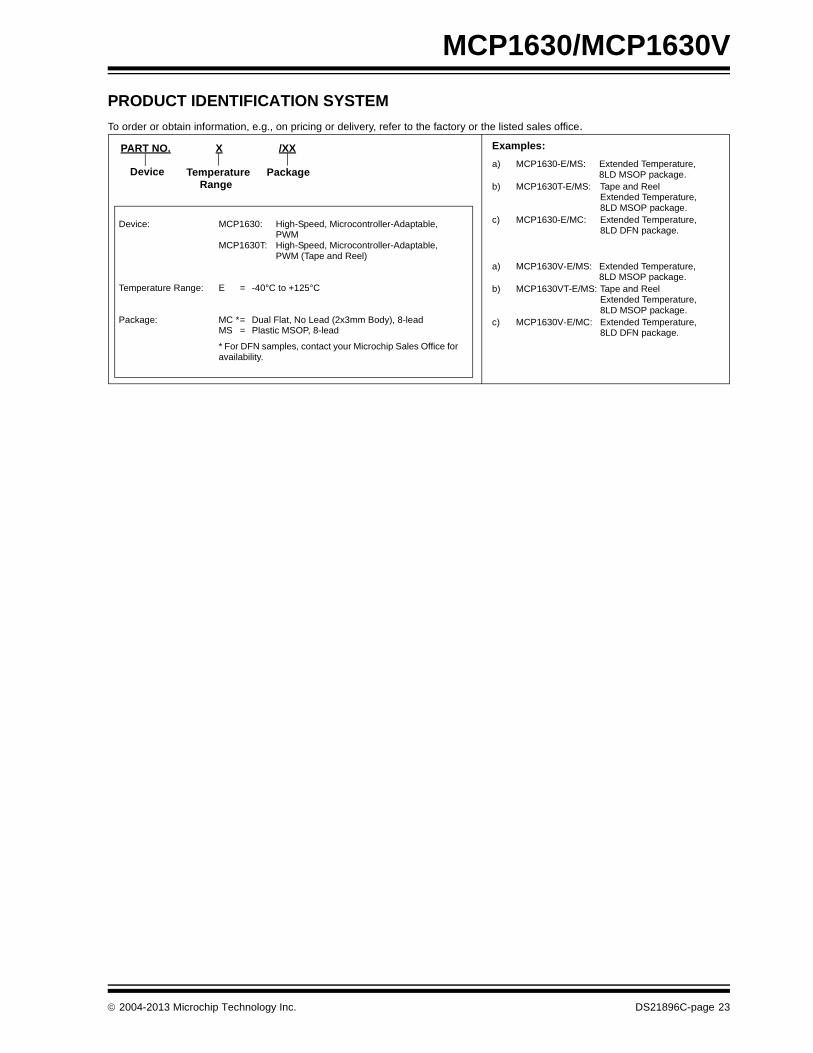
PRODUCT IDENTIFICATION SYSTEM
To order or obtain information, e.g., on pricing or delivery, refer to the factory or the listed sales office.
Device: MCP1630: High-Speed, Microcontroller-Adaptable, PWM
MCP1630T: High-Speed, Microcontroller-Adaptable, PWM (Tape and Reel)
Temperature Range: E = -40°C to +125°C
Package: MC *= Dual Flat, No Lead (2x3mm Body), 8-leadMS = Plastic MSOP, 8-lead
* For DFN samples, contact your Microchip Sales Office for availability.
PART NO. X /XX
PackageTemperatureRange
Device
Examples:
a) MCP1630-E/MS: Extended Temperature,8LD MSOP package.
b) MCP1630T-E/MS: Tape and ReelExtended Temperature,8LD MSOP package.
c) MCP1630-E/MC: Extended Temperature,8LD DFN package.
a) MCP1630V-E/MS: Extended Temperature,8LD MSOP package.
b) MCP1630VT-E/MS: Tape and ReelExtended Temperature,8LD MSOP package.
c) MCP1630V-E/MC: Extended Temperature,8LD DFN package.
2004-2013 Microchip Technology Inc. DS21896C-page 23

MCP1630/MCP1630V
NOTES:
DS21896C-page 24 2004-2013 Microchip Technology Inc.

Note the following details of the code protection feature on Microchip devices:
• Microchip products meet the specification contained in their particular Microchip Data Sheet.
• Microchip believes that its family of products is one of the most secure families of its kind on the market today, when used in the intended manner and under normal conditions.
• There are dishonest and possibly illegal methods used to breach the code protection feature. All of these methods, to our knowledge, require using the Microchip products in a manner outside the operating specifications contained in Microchip’s Data Sheets. Most likely, the person doing so is engaged in theft of intellectual property.
• Microchip is willing to work with the customer who is concerned about the integrity of their code.
• Neither Microchip nor any other semiconductor manufacturer can guarantee the security of their code. Code protection does not mean that we are guaranteeing the product as “unbreakable.”
Code protection is constantly evolving. We at Microchip are committed to continuously improving the code protection features of ourproducts. Attempts to break Microchip’s code protection feature may be a violation of the Digital Millennium Copyright Act. If such actsallow unauthorized access to your software or other copyrighted work, you may have a right to sue for relief under that Act.
Information contained in this publication regarding deviceapplications and the like is provided only for your convenienceand may be superseded by updates. It is your responsibility toensure that your application meets with your specifications.MICROCHIP MAKES NO REPRESENTATIONS ORWARRANTIES OF ANY KIND WHETHER EXPRESS ORIMPLIED, WRITTEN OR ORAL, STATUTORY OROTHERWISE, RELATED TO THE INFORMATION,INCLUDING BUT NOT LIMITED TO ITS CONDITION,QUALITY, PERFORMANCE, MERCHANTABILITY ORFITNESS FOR PURPOSE. Microchip disclaims all liabilityarising from this information and its use. Use of Microchipdevices in life support and/or safety applications is entirely atthe buyer’s risk, and the buyer agrees to defend, indemnify andhold harmless Microchip from any and all damages, claims,suits, or expenses resulting from such use. No licenses areconveyed, implicitly or otherwise, under any Microchipintellectual property rights.
2004-2013 Microchip Technology Inc.
QUALITY MANAGEMENT SYSTEM CERTIFIED BY DNV
== ISO/TS 16949 ==
Trademarks
The Microchip name and logo, the Microchip logo, dsPIC, FlashFlex, KEELOQ, KEELOQ logo, MPLAB, PIC, PICmicro, PICSTART, PIC32 logo, rfPIC, SST, SST Logo, SuperFlash and UNI/O are registered trademarks of Microchip Technology Incorporated in the U.S.A. and other countries.
FilterLab, Hampshire, HI-TECH C, Linear Active Thermistor, MTP, SEEVAL and The Embedded Control Solutions Company are registered trademarks of Microchip Technology Incorporated in the U.S.A.
Silicon Storage Technology is a registered trademark of Microchip Technology Inc. in other countries.
Analog-for-the-Digital Age, Application Maestro, BodyCom, chipKIT, chipKIT logo, CodeGuard, dsPICDEM, dsPICDEM.net, dsPICworks, dsSPEAK, ECAN, ECONOMONITOR, FanSense, HI-TIDE, In-Circuit Serial Programming, ICSP, Mindi, MiWi, MPASM, MPF, MPLAB Certified logo, MPLIB, MPLINK, mTouch, Omniscient Code Generation, PICC, PICC-18, PICDEM, PICDEM.net, PICkit, PICtail, REAL ICE, rfLAB, Select Mode, SQI, Serial Quad I/O, Total Endurance, TSHARC, UniWinDriver, WiperLock, ZENA and Z-Scale are trademarks of Microchip Technology Incorporated in the U.S.A. and other countries.
SQTP is a service mark of Microchip Technology Incorporated in the U.S.A.
GestIC and ULPP are registered trademarks of Microchip Technology Germany II GmbH & Co. & KG, a subsidiary of Microchip Technology Inc., in other countries.
All other trademarks mentioned herein are property of their respective companies.
© 2004-2013, Microchip Technology Incorporated, Printed in the U.S.A., All Rights Reserved.
Printed on recycled paper.
ISBN: 9781620769140
Microchip received ISO/TS-16949:2009 certification for its worldwide
DS21896C-page 25
headquarters, design and wafer fabrication facilities in Chandler and Tempe, Arizona; Gresham, Oregon and design centers in California and India. The Company’s quality system processes and procedures are for its PIC® MCUs and dsPIC® DSCs, KEELOQ® code hopping devices, Serial EEPROMs, microperipherals, nonvolatile memory and analog products. In addition, Microchip’s quality system for the design and manufacture of development systems is ISO 9001:2000 certified.

DS21896C-page 26 2004-2013 Microchip Technology Inc.
AMERICASCorporate Office2355 West Chandler Blvd.Chandler, AZ 85224-6199Tel: 480-792-7200 Fax: 480-792-7277Technical Support: http://www.microchip.com/supportWeb Address: www.microchip.com
AtlantaDuluth, GA Tel: 678-957-9614 Fax: 678-957-1455
BostonWestborough, MA Tel: 774-760-0087 Fax: 774-760-0088
ChicagoItasca, IL Tel: 630-285-0071 Fax: 630-285-0075
ClevelandIndependence, OH Tel: 216-447-0464 Fax: 216-447-0643
DallasAddison, TX Tel: 972-818-7423 Fax: 972-818-2924
DetroitFarmington Hills, MI Tel: 248-538-2250Fax: 248-538-2260
IndianapolisNoblesville, IN Tel: 317-773-8323Fax: 317-773-5453
Los AngelesMission Viejo, CA Tel: 949-462-9523 Fax: 949-462-9608
Santa ClaraSanta Clara, CA Tel: 408-961-6444Fax: 408-961-6445
TorontoMississauga, Ontario, CanadaTel: 905-673-0699 Fax: 905-673-6509
ASIA/PACIFICAsia Pacific OfficeSuites 3707-14, 37th FloorTower 6, The GatewayHarbour City, KowloonHong KongTel: 852-2401-1200Fax: 852-2401-3431
Australia - SydneyTel: 61-2-9868-6733Fax: 61-2-9868-6755
China - BeijingTel: 86-10-8569-7000 Fax: 86-10-8528-2104
China - ChengduTel: 86-28-8665-5511Fax: 86-28-8665-7889
China - ChongqingTel: 86-23-8980-9588Fax: 86-23-8980-9500
China - HangzhouTel: 86-571-2819-3187 Fax: 86-571-2819-3189
China - Hong Kong SARTel: 852-2943-5100 Fax: 852-2401-3431
China - NanjingTel: 86-25-8473-2460Fax: 86-25-8473-2470
China - QingdaoTel: 86-532-8502-7355Fax: 86-532-8502-7205
China - ShanghaiTel: 86-21-5407-5533 Fax: 86-21-5407-5066
China - ShenyangTel: 86-24-2334-2829Fax: 86-24-2334-2393
China - ShenzhenTel: 86-755-8864-2200 Fax: 86-755-8203-1760
China - WuhanTel: 86-27-5980-5300Fax: 86-27-5980-5118
China - XianTel: 86-29-8833-7252Fax: 86-29-8833-7256
China - XiamenTel: 86-592-2388138 Fax: 86-592-2388130
China - ZhuhaiTel: 86-756-3210040 Fax: 86-756-3210049
ASIA/PACIFICIndia - BangaloreTel: 91-80-3090-4444 Fax: 91-80-3090-4123
India - New DelhiTel: 91-11-4160-8631Fax: 91-11-4160-8632
India - PuneTel: 91-20-2566-1512Fax: 91-20-2566-1513
Japan - OsakaTel: 81-6-6152-7160 Fax: 81-6-6152-9310
Japan - TokyoTel: 81-3-6880- 3770 Fax: 81-3-6880-3771
Korea - DaeguTel: 82-53-744-4301Fax: 82-53-744-4302
Korea - SeoulTel: 82-2-554-7200Fax: 82-2-558-5932 or 82-2-558-5934
Malaysia - Kuala LumpurTel: 60-3-6201-9857Fax: 60-3-6201-9859
Malaysia - PenangTel: 60-4-227-8870Fax: 60-4-227-4068
Philippines - ManilaTel: 63-2-634-9065Fax: 63-2-634-9069
SingaporeTel: 65-6334-8870Fax: 65-6334-8850
Taiwan - Hsin ChuTel: 886-3-5778-366Fax: 886-3-5770-955
Taiwan - KaohsiungTel: 886-7-213-7828Fax: 886-7-330-9305
Taiwan - TaipeiTel: 886-2-2508-8600 Fax: 886-2-2508-0102
Thailand - BangkokTel: 66-2-694-1351Fax: 66-2-694-1350
EUROPEAustria - WelsTel: 43-7242-2244-39Fax: 43-7242-2244-393Denmark - CopenhagenTel: 45-4450-2828 Fax: 45-4485-2829
France - ParisTel: 33-1-69-53-63-20 Fax: 33-1-69-30-90-79
Germany - MunichTel: 49-89-627-144-0 Fax: 49-89-627-144-44
Italy - Milan Tel: 39-0331-742611 Fax: 39-0331-466781
Netherlands - DrunenTel: 31-416-690399 Fax: 31-416-690340
Spain - MadridTel: 34-91-708-08-90Fax: 34-91-708-08-91
UK - WokinghamTel: 44-118-921-5869Fax: 44-118-921-5820
Worldwide Sales and Service
11/29/12