Modeling, Analysis and Design of High-Speed Links - Rethinking

High-speed data communication links for
high energy physics experiments
Shalabh Gupta ([email protected])
Associate Professor
Department of Electrical Engineering, IIT Bombay
Powai, Mumbai – 400076, INDIA
October 6, 2017
ASET COLLOQUIUM / NSPDI 2017
Tata Institute of Fundamental Research, Mumbai

Need for High-Speed
Communication Links Explosive growth in the Internet traffic
– Solution: Use of coherent modulation and detection: Electronics – the key enabler!
– Optical links with 200 – 400 Gbps/wavelength being developed
and deployed for long haul.
Global Data Center IP Traffic Forecast
Recent Focus: Data Centers
High-capacity long haul links
have been there for a while.
Focus now shifting to short
distance Tbps optical
interconnects
OFC 2016
OFC 2017 Panel
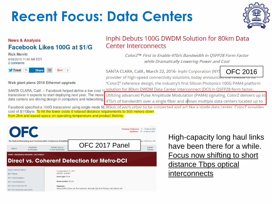
CMS Detector @CERN
Courtesy: http://cms.web.cern.ch/news/cms-detector-design
Can generate data @40 Tb/s
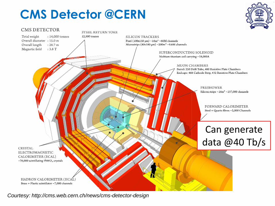
Outline
• High-speed serial links: Basic overview
– Clocking / Clock and Data Recovery
– Serializers & Deserializers
– Current progress in high-speed serial links
– Considerations – for HEP experiments
• Optical communication links: An overview
• Current trends: Digital Coherent Transmission
Systems
• Research at IIT Bombay: Low power
coherent optical links

Disclaimer: Have no exposure to the
HEP experiments myself!
Problem Statement
• Millions of sensor channels produce tens of
Terabits/second of data
• Data from various channels has to be
aggregated and transferred to central/remote
locations for processing/storage
• Latency has to be minimized for triggers and
control
• Power efficiency may also be important
(adversely affect the temperatures in the
detector)

Overview of high-speed serial
links
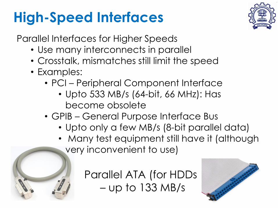
High-Speed Interfaces
Parallel Interfaces for Higher Speeds
• Use many interconnects in parallel
• Crosstalk, mismatches still limit the speed
• Examples:
• PCI – Peripheral Component Interface
• Upto 533 MB/s (64-bit, 66 MHz): Has
become obsolete
• GPIB – General Purpose Interface Bus
• Upto only a few MB/s (8-bit parallel data)
• Many test equipment still have it (although
very inconvenient to use)
Parallel ATA (for HDDs
– up to 133 MB/s

High-Speed Serial Interfaces
High-Speed Serial Interfaces
• Smaller form factor / area on PCB
• Faster speeds
• Lower power
• More reliable
• Examples
• USB (v1.0: 1.5 Mbit/s to v3.1: 10 Gbit/s)
• HDMI (v1.0: 1.65 Gbps/lane to v2.1: 12 Gbps/lane)
• PCIe: PCI-Express (v1.0: 2.5 Gbps/lane to v4.0: 16
Gbps/lane, upto 16 lanes)
• SATA (upto 16 Gbps) for HDD access

High-Speed Serial Interfaces: Key Enablers
• Low-voltage differential signaling
• Common-mode noise is suppressed
• Results in lower power consumption
• Availability of fast, low power, low cost
electronics
• Clock recovery/alignment techniques
• Equalization techniques
• Line coding techniques
• Error correction coding/decoding
• Necessity!!

Need for High-Speed Serial Links
• Higher speed links: Some more examples– Communication between ADC/DACs and FPGAs/DSP
• Example: A quad of 16-bits 1-GS/s DAC (used in Mobile
base-stations) – requires 64 Gbps delivered to the chip • Automotive industry – Self driven cars
• Satellites: Communications, Imagery data
• Data Centers – Working as Clouds
Type
Max
Performance
(Gbps)
Max
Transceivers
Peak Bandwidth
(bidirectional)
Virtex
UltraScale+GTY 32.75 128 8,384 Gb/s
Kintex
UltraScale+GTH/GTY 16.3/32.75 44/32 3,268 Gb/s
Virtex
UltraScaleGTH/GTY 16.3/30.5 60/60 5,616 Gb/s
Kintex
UltraScaleGTH 16.3 64 2,086 Gb/s
Virtex-7 GTX/GTH/GTZ 12.5/13.1/28.05 56/96/163 2,784 Gb/s
Kintex-7 GTX 12.5 32 800 Gb/s
Artix-7 GTP 6.6 16 211 Gb/s
Zynq
UltraScale+GTR/GTH/GTY 6.0/16.3/32.75 4/44/28 3,268 Gb/s
Zynq-7000 GTX 12.5 16 400 Gb/s
Spartan-6 GTP 3.2 8 51 Gb/s
Xilinx FPGAs Available (Feb. ’17)

Challenges in Serial Links
• Digital data signals no longer appear to have well defined HIGH or LOW levels.
• There is significant ISI (Inter-Symbol-Interference) due to
Impedance mismatches
Limited bandwidth of the channel
• Due to ISI, poor eye opening is obtained
High BER or no signal detection at all!
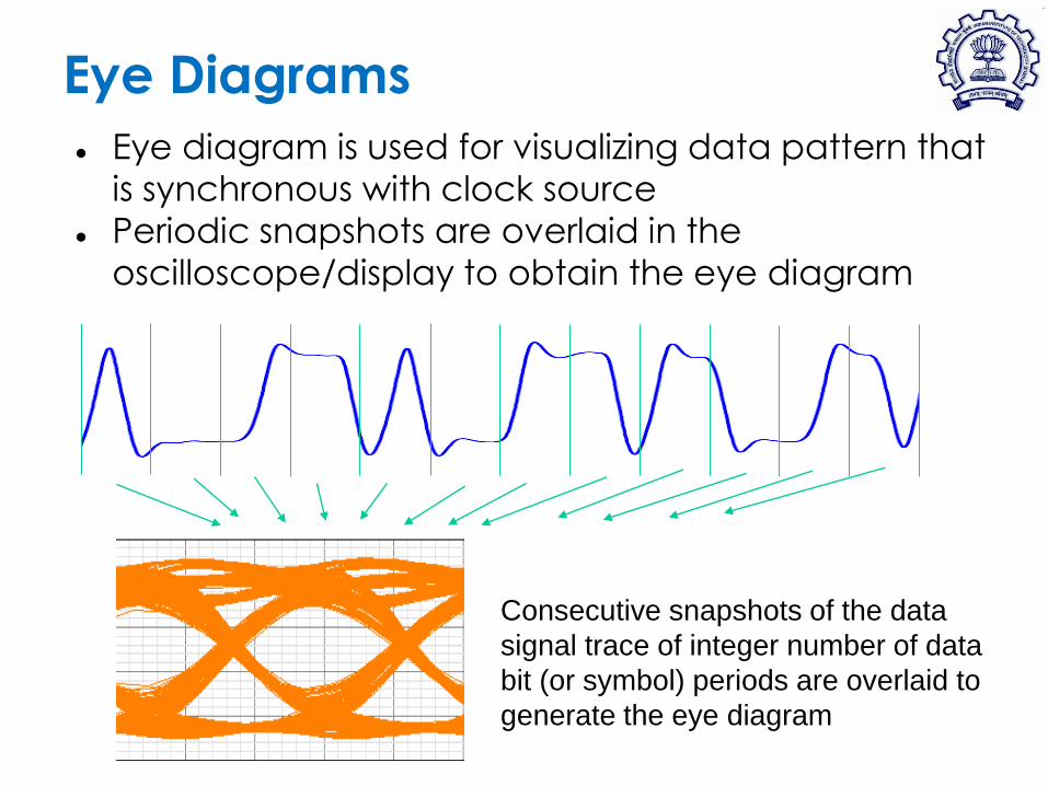
Eye Diagrams
Eye diagram is used for visualizing data pattern that
is synchronous with clock source
Periodic snapshots are overlaid in the
oscilloscope/display to obtain the eye diagram
Consecutive snapshots of the data
signal trace of integer number of data
bit (or symbol) periods are overlaid to
generate the eye diagram

Eye Diagrams: Example
[Beyene, IEEE
TAP, 2008]
Eye diagram for PAM-4
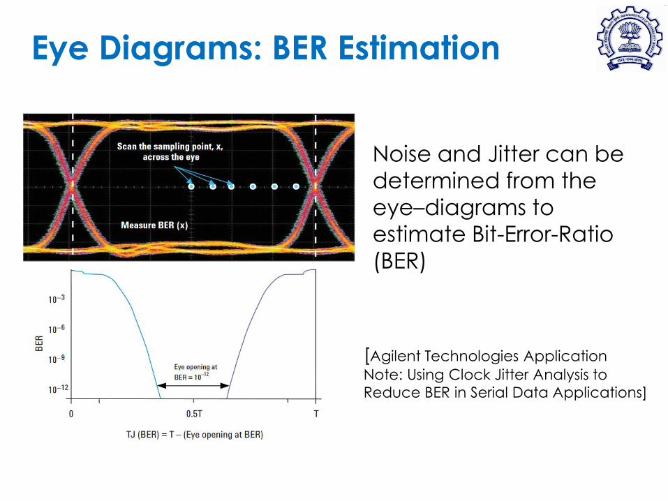
Eye Diagrams: BER Estimation
Noise and Jitter can be
determined from the
eye–diagrams to
estimate Bit-Error-Ratio
(BER)
[Agilent Technologies Application
Note: Using Clock Jitter Analysis to
Reduce BER in Serial Data Applications]

Clocking in High-Speed Serial
Interfaces
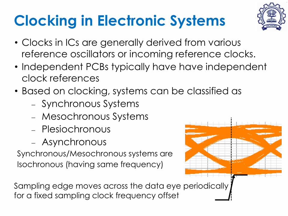
Clocking in Electronic Systems
• Clocks in ICs are generally derived from various reference oscillators or incoming reference clocks.
• Independent PCBs typically have have independent clock references
• Based on clocking, systems can be classified as
Synchronous Systems
Mesochronous Systems
Plesiochronous
AsynchronousSynchronous/Mesochronous systems are
Isochronous (having same frequency)
Sampling edge moves across the data eye periodically
for a fixed sampling clock frequency offset

Synchronous System
• Clock and data are aligned in phase
• Possible for low speed systems, such as SPI bus, low rate serial or parallel interfaces
Good for configuring the ICs (easy to design and reliable)
• Not possible to use them for high speeds, and
unattractive for long interconnects (as an additional wire for the clock is required).
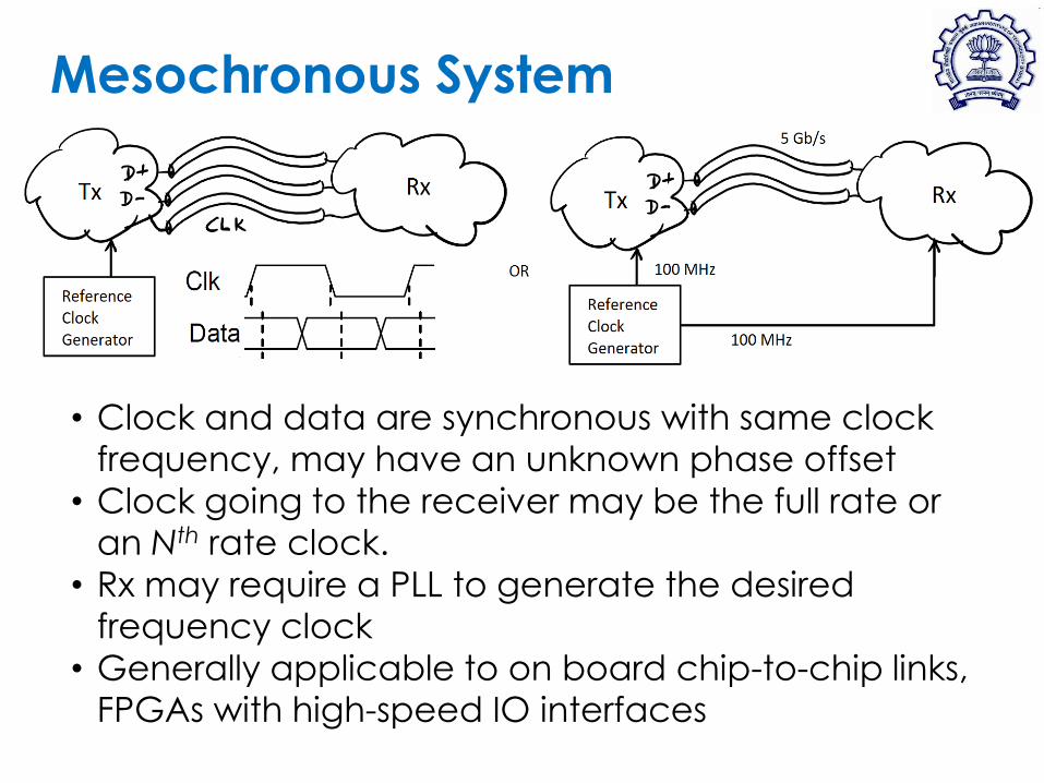
Mesochronous System
• Clock and data are synchronous with same clock frequency, may have an unknown phase offset
• Clock going to the receiver may be the full rate or an Nth rate clock.
• Rx may require a PLL to generate the desired frequency clock
• Generally applicable to on board chip-to-chip links, FPGAs with high-speed IO interfaces

Plesiochronous System
• The reference clocks for the two systems may have a small frequency offset (although they’re meant to be the same).
Even a 1-Hz offset causes the data clock phase to shift by 2p in 1 second.
• Clock embedded clock must be recovered from the incoming
signal
• To adjust for frequency difference between the Tx and Rx clock domains.
• Rx has to employ a FIFO buffer
• Tx has to send a few redundant words that can be dropped by the Rx if the it clock frequency is slower.
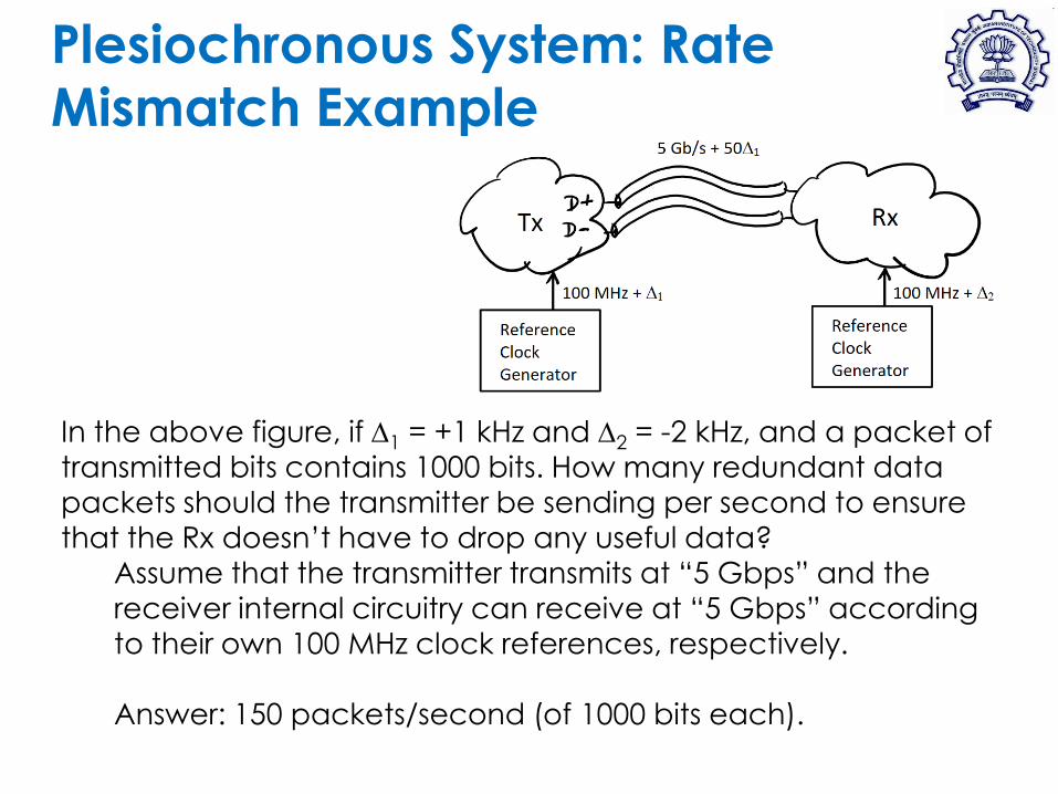
Plesiochronous System: Rate Mismatch Example
In the above figure, if D1 = +1 kHz and D2 = -2 kHz, and a packet of
transmitted bits contains 1000 bits. How many redundant data
packets should the transmitter be sending per second to ensure
that the Rx doesn’t have to drop any useful data?
Assume that the transmitter transmits at “5 Gbps” and the receiver internal circuitry can receive at “5 Gbps” according
to their own 100 MHz clock references, respectively.
Answer: 150 packets/second (of 1000 bits each).

Asynchronous System
• The reference clocks for the two systems are independent
• Transfer of data is generally packed based and the data transfer
rate is not very well defined
• For example, some standard baud rates used in UARTs in bps include 300, 1200, 2400, 4800, 9600, 14400, 19200
Transitions between stop/start bits are used for “synchronizing” at the byte level (for a given approximate baud rate)
• Sometimes handshake signals used for data transmission
• Greatly limits the transfer rates.

SerDes for Mesochronous Systems
• High speed serial links comprise SerDes (Serializer-Deserializer)
• Mostly used in Mesochronous or Plesiochronous Systems
• May include pre-emphasis filter at Tx output and feed-forward/decision-feedback equalizer at Rx input
• No need to clock recovery and FIFO for rate matching in Mesochronous systems

SerDes for Plesiochronous Systems
• Receiver requires a clock recovery circuit to recover the clock embedded in the data signal
• Two system clocks: Tx and Rx rates have a mismatch
• FIFO buffer has to be added in the digital domain to take care of the rate mismatch
Some redundant packets are added at the Tx, which may be dropped by FIFO if Tx clock is faster than Rx clock

De-Serializers: Phase Alignment
Deserializers require alignment of clock-phase wrt the
data signal to sample the data correctly
• Mesochronous systems: Require a Delay-Locked-
Loop (DLL) for clock phase alignment
• Synchronous systems: Require a Phased-Locked-Loop (PLL) for clock recovery and phase alignment
DLLs and PLLs
A Delay Locked Loop adds the desired phase
shift (or delay) to the periodic input signal
using a feedback technique.
A Phase Locked Loop generates a periodic
signal with a well-defined phase with
reference to a periodic or clock synchronous
input signal.
A PLL has an inbuilt tunable oscillator, whereas
a DLL has tunable delay element(s) but NO
oscillator!

Delay Locked Loops
A delay locked loop (DLL) aligns the input clock phase
with respect to the input signal
• Typically provides an output clock that is a phase
shifted version of the input clock
Well defined
phase wrt Din
CKin CKout
Din
Arbitrary
phase wrt Din

Delay Locked Loops
A delay locked loop can be used for consists of
• Phase Detector
• Charge Pump (optional)
• Loop filter (or a low pass filter)
• Tunable delay blocks
Can use for
• clock alignment with data
• multi-phase clock generation

Delay Locked Loops: Half-Rate PD with 1:2 Demux
Din
CKin
CKout
Dout, even Dout, odd Dout, even
Half-rate: The
input clock
frequency is half
the input data-
rate
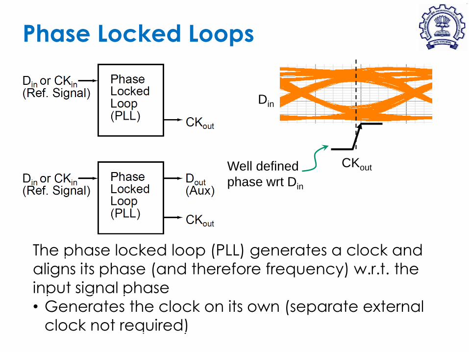
Phase Locked Loops
The phase locked loop (PLL) generates a clock and
aligns its phase (and therefore frequency) w.r.t. the
input signal phase
• Generates the clock on its own (separate external
clock not required)
Well defined
phase wrt Din
CKout
Din
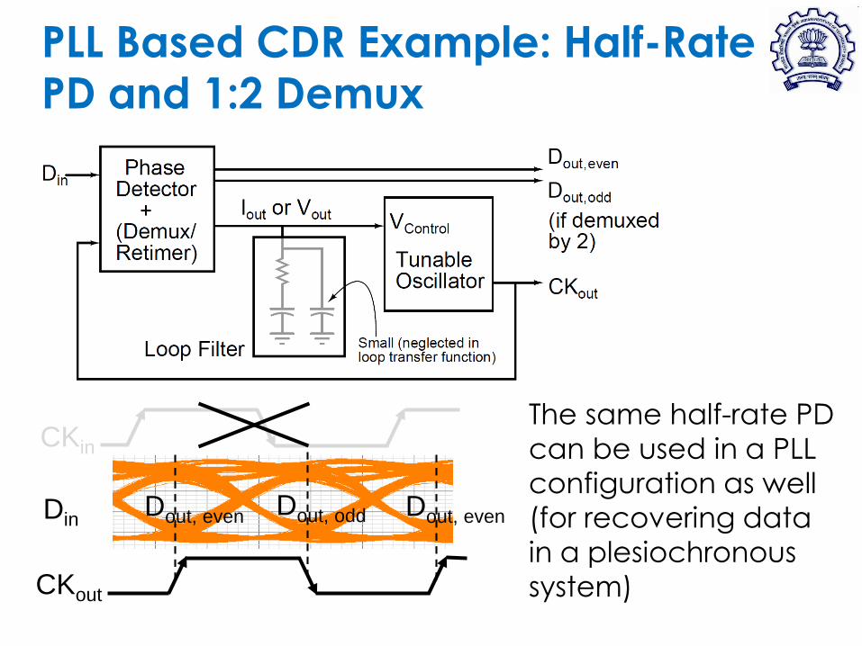
PLL Based CDR Example: Half-RatePD and 1:2 Demux
Din
CKin
CKout
Dout, even Dout, odd Dout, even
The same half-rate PD
can be used in a PLL
configuration as well
(for recovering data
in a plesiochronous
system)

DLLs vs. PLLs
Property DLLs PLLs
Tunable block Delay(s) Oscillator
Loop transfer
function
Has one pole at zero
frequency
Has at least two poles at
zero frequency
Loop filter One pole is sufficient Has a pole; should also
have a zero for stability
Application in
Serial Links
Data Recovery
(Mesochronous Systems)
Clock and Data Recovery
(Plesiochronous Systems)
Stability Unconditionally stable Stability NOT guaranteed
(requires careful analysis)
Loop
Bandwidth
High (fast locking and
tracking)
Low (slow locking and
tracking)
Jitter response Transparent to ref. clock
jitter (ref clock and data
jitters track each other)
Low pass filter input jitter;
High pass filter VCO jitter.
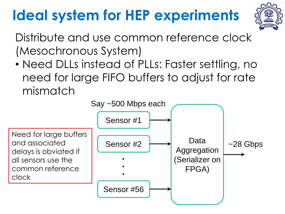
Ideal system for HEP experiments
Distribute and use common reference clock
(Mesochronous System)
• Need DLLs instead of PLLs: Faster settling, no
need for large FIFO buffers to adjust for rate
mismatch
Sensor #1
Data
Aggregation
(Serializer on
FPGA)
Sensor #2
Sensor #56
Say ~500 Mbps each
~28 Gbps
Need for large buffers
and associated
delays is obviated if
all sensors use the
common reference
clock
•
•
•

Other Aspects of Serial Links
• Need for line-coding schemes (such as 8b-
10b or 64b-66b) to aid clock recovery and
framing bits (depending on protocols)
• Equalization required to compensate for
low-pass nature of the channel
• PAM-4 for higher bit-rates
where channel is bandwidth
limited and not SNR limited
Eye diagram for PAM-4

Optical Interfaces
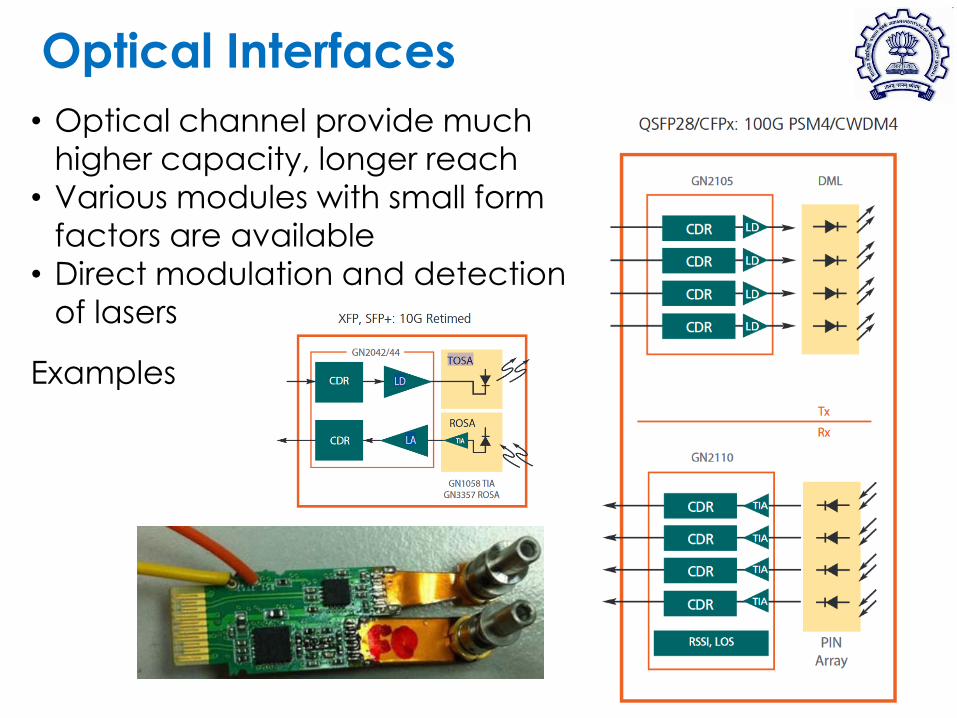
Optical Interfaces
• Optical channel provide much
higher capacity, longer reach
• Various modules with small form
factors are available
• Direct modulation and detection
of lasers
Examples

Optical Links: Historical
Perspective
Direct Modulation Direct Detection• Common in legacy links
• Still power hungry, spectrally inefficient.
• Wavelength division multiplexing can also be used
• 100GbE short distance links use 4 lambdas or PAM-4/PAM-8 for spectral efficiency, lower power

Optical Links: Coherent Systems
Coherent Systems – Receiver needs reference phase to demodulation message
– Linear w.r.t optical field (direct detection is a non-linear process, difficult to invert the channel)
– Serious research started in early 1980s
Abandoned: Difficult; DMDD with WDM was sufficient at that time!
Richard A. Linke and Paul S. Henry
IEEE Spectrum, February 1987

Progress in the last 10 Years
High-speed coherent research picked up again in ~2006
• Coherent 100Gbps DP-QPSK products easily available
• Record breaking results achieved (Pbits/s with DWDM and dense
constellation such as 128-QAM)
• Key Enabler: Electronics (DSOs, AWGs, ADCs and DSPs)!
• Focus now on short distance links for data centers!

Coherent Optical Links
Coherent links: 100-Gbps / l and beyond– Both amplitude/phase of optical field modulated at transmitter
– Coherent detection at receiver (optical field is mixed with a local oscillator) to measure complex optical field (both amplitude and phase)
– Polarization multiplexing possible (due to linearity)
– Currently used only for long haul
Optional EssentialSource: Infinera
Formats such as 64-QAM
also possible
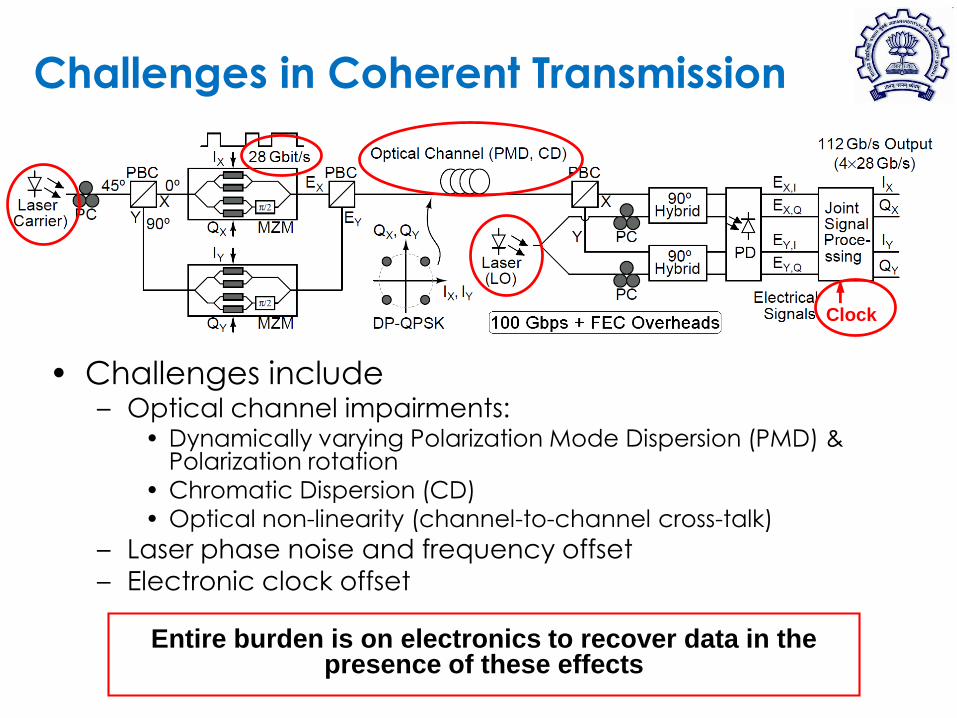
Challenges in Coherent Transmission
• Challenges include– Optical channel impairments:
• Dynamically varying Polarization Mode Dispersion (PMD) & Polarization rotation
• Chromatic Dispersion (CD)
• Optical non-linearity (channel-to-channel cross-talk)
– Laser phase noise and frequency offset
– Electronic clock offset
Entire burden is on electronics to recover data in the presence of these effects
Clock

Recent Focus: Data Centers
High-capacity long haul links
have been there for a while.
Focus now shifting to short
distance Tbps optical
interconnects
OFC 2016
OFC 2017 Panel

Power Consumption in Data Centers
C. Belady, “Data Center Power Projections to 2014,” ITHERM 2006.
Power and cooling costs already higher than the cost of IT
equipment in data centers

Coherent Rx: Analog Domain
Signal Processing
Analog processing well suited for this application – Power efficient at these speeds
– Much faster feedback control possible: easy compensation of dynamic changes (such as carrier frequency offsets)
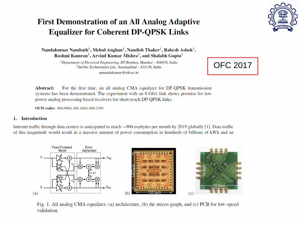
OFC 2017
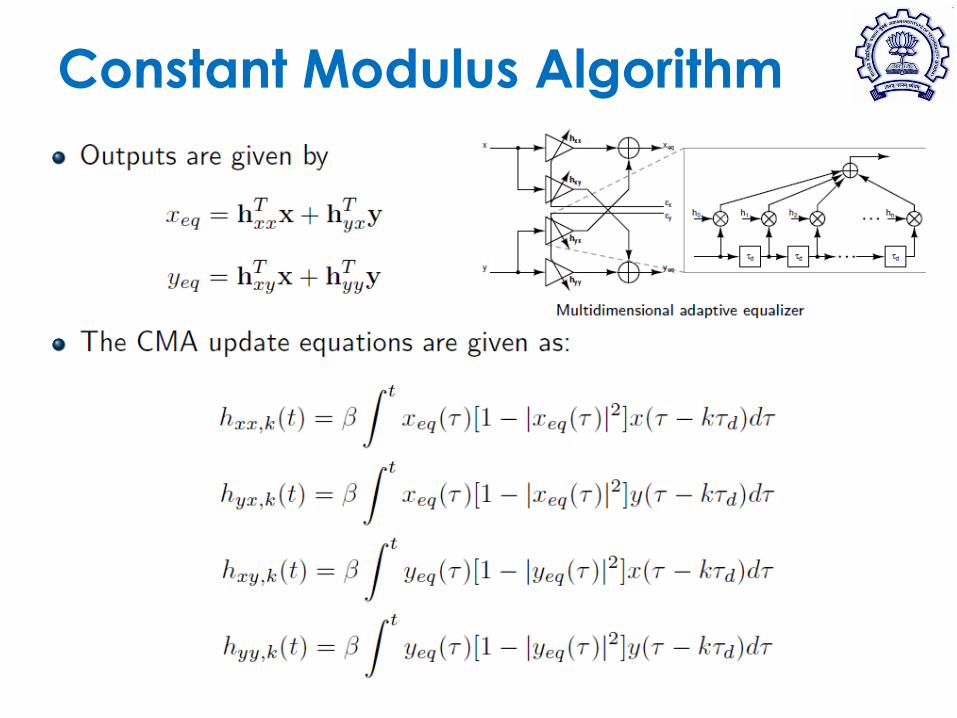
Constant Modulus Algorithm

Equalizer Implementation in
130nm BiCMOS Technology
Chip area = 1.4mm1.35 mm, Power = 2.5W; Baud Rate: 25 Gbaud
Can be reduced further with advanced CMOS
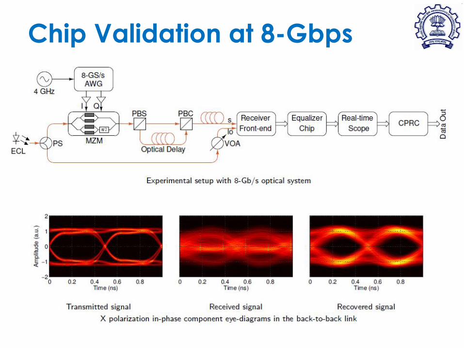
Chip Validation at 8-Gbps
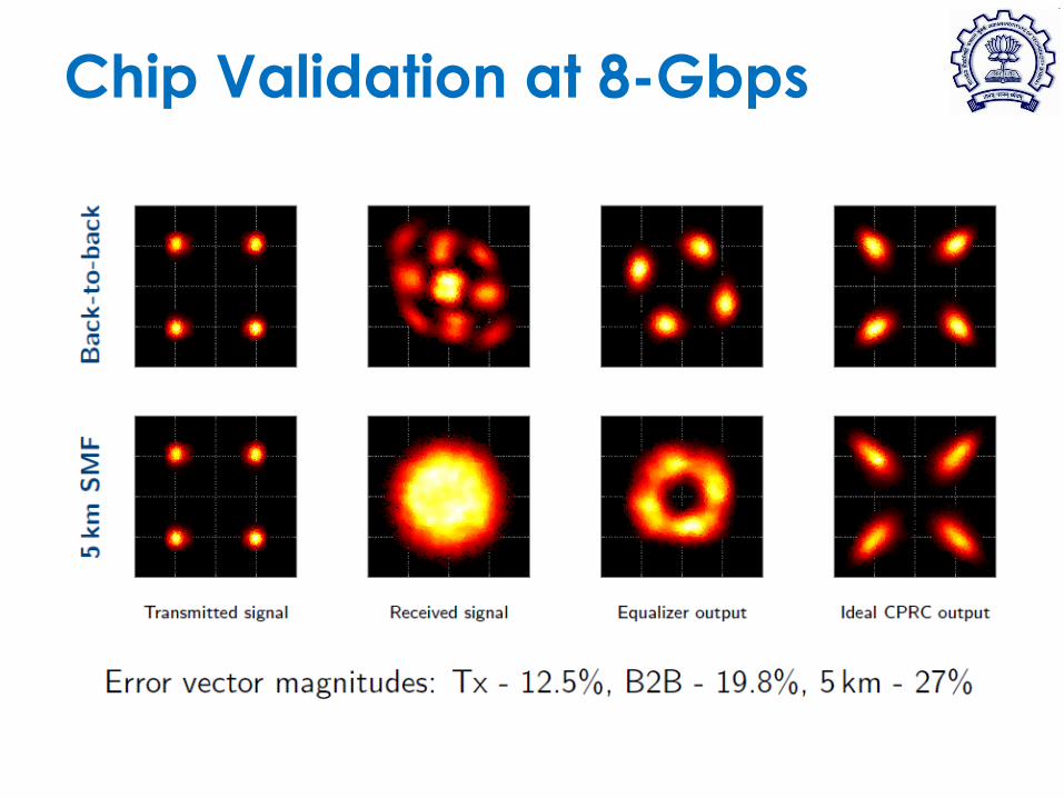
Chip Validation at 8-Gbps

Further simplification of the receiver:
Self-homodyne (LO-less receiver)
WOCC 2017
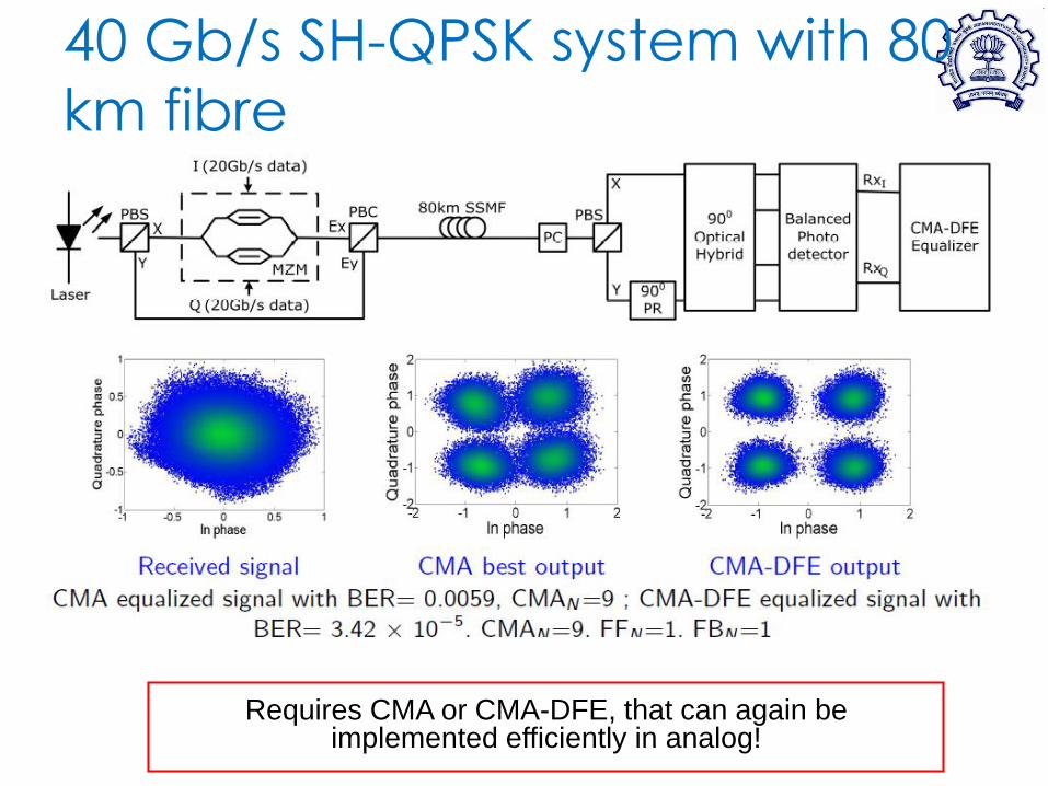
40 Gb/s SH-QPSK system with 80
km fibre
Requires CMA or CMA-DFE, that can again be implemented efficiently in analog!

Longer Term Vision: Ultra Low Power
Tbps Optical Interconnects
• Use analog domain signal processing for low power
consumption/form factor for short range coherent systems
• Simplified system using self-homodyne receiver.
• Use PICs along with analog processing for further reduction in
power consumption and longer reach!
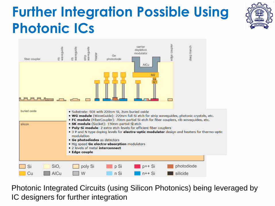
Further Integration Possible Using
Photonic ICs
Photonic Integrated Circuits (using Silicon Photonics) being leveraged by
IC designers for further integration
Acknowledgement
Would like to thank
• A large number of dedicated students and
project associates who contributed to the
project
• MeitY and DST (Govt. of India) for funding
the projects
• Sterlite Technologies for giving access to
their lab facilities for carrying out some of
the experiments