Characterizing High-Speed Serial Communications Links Requires Some Analog Savvy_wiht_Figures
23
Characterizing High-Speed Serial Communications Links Requires Some Analog Savvy A six-step process helps measure, identify, and eliminate clock and data jitter on those blazing serial signals. Dec 1, 2008Hamed M. Sanogo Electronic Design As serial-data standards go from fast to very fast, designers must devote a greater amount of time to the analog features of those high-speed signals. It’s no longer enough to remain in the digital domain with ones and zeros. To find and correct conditions that lead to potential problems—and thereby prevent those problems from showing up in the field—designers must check the parametric realm of their designs. Signal integrity (SI) engineers have to mitigate or eliminate the effects of timing jitter on system performance. The following discussion offers a simple and practical procedure for characterizing high-speed serial data links at 1Gbps and beyond. The characterization of a high-speed serial link depends on the ability of the SI engineer to find, understand, and solve serious jitter problems. In this discussion, we assume that the clock and data recovery (CDR) block of the PHY (physical layer) or SERDES (serializer- deserializer) device complies with the standards applicable to that device. In a serial communication system, the CDR recovers the clock signal from the data stream. Therefore, a key operation is to extract data from the serial data stream and synchronize it with the data-transmitter clock.
-
Upload
hamed-m-sanogo -
Category
Documents
-
view
23 -
download
2
Transcript of Characterizing High-Speed Serial Communications Links Requires Some Analog Savvy_wiht_Figures

Characterizing High-Speed Serial Communications Links Requires Some Analog Savvy
A six-step process helps measure, identify, and eliminate clock and data jitter on those blazing serial signals.
Dec 1, 2008Hamed M. Sanogo Electronic Design
As serial-data standards go from fast to very fast, designers must devote a greater amount of
time to the analog features of those high-speed signals. It’s no longer enough to remain in
the digital domain with ones and zeros. To find and correct conditions that lead to potential
problems—and thereby prevent those problems from showing up in the field—designers
must check the parametric realm of their designs. Signal integrity (SI) engineers have to
mitigate or eliminate the effects of timing jitter on system performance. The following
discussion offers a simple and practical procedure for characterizing high-speed serial data
links at 1Gbps and beyond.
The characterization of a high-speed serial link depends on the ability of the SI engineer to
find, understand, and solve serious jitter problems. In this discussion, we assume that the
clock and data recovery (CDR) block of the PHY (physical layer) or SERDES (serializer-
deserializer) device complies with the standards applicable to that device. In a serial
communication system, the CDR recovers the clock signal from the data stream. Therefore,
a key operation is to extract data from the serial data stream and synchronize it with the
data-transmitter clock.
The transmitter always contributes some jitter to the recovered clock, but let’s assume that
contribution to be minimal. For the purpose of simplification, we’ll assume any jitter seen
on the recovered clock to have been coupled either onto the link in the cable (as EMI) or
within the PCB (as cross-talk).
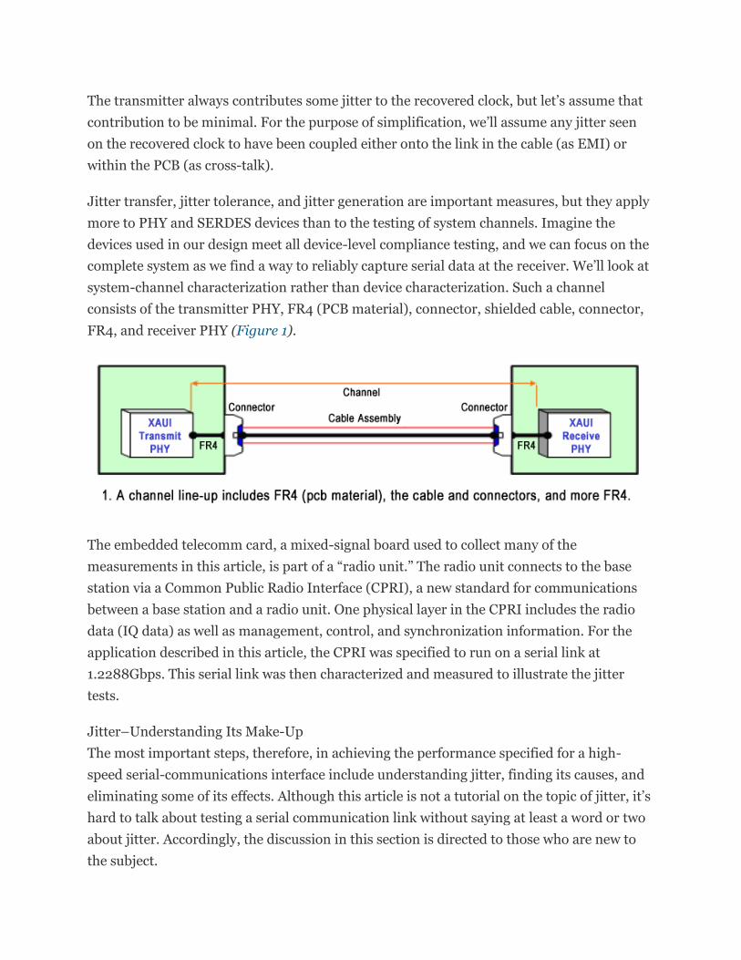
Jitter transfer, jitter tolerance, and jitter generation are important measures, but they apply
more to PHY and SERDES devices than to the testing of system channels. Imagine the
devices used in our design meet all device-level compliance testing, and we can focus on the
complete system as we find a way to reliably capture serial data at the receiver. We’ll look at
system-channel characterization rather than device characterization. Such a channel
consists of the transmitter PHY, FR4 (PCB material), connector, shielded cable, connector,
FR4, and receiver PHY (Figure 1).
The embedded telecomm card, a mixed-signal board used to collect many of the
measurements in this article, is part of a “radio unit.” The radio unit connects to the base
station via a Common Public Radio Interface (CPRI), a new standard for communications
between a base station and a radio unit. One physical layer in the CPRI includes the radio
data (IQ data) as well as management, control, and synchronization information. For the
application described in this article, the CPRI was specified to run on a serial link at
1.2288Gbps. This serial link was then characterized and measured to illustrate the jitter
tests.
Jitter–Understanding Its Make-Up
The most important steps, therefore, in achieving the performance specified for a high-
speed serial-communications interface include understanding jitter, finding its causes, and
eliminating some of its effects. Although this article is not a tutorial on the topic of jitter, it’s
hard to talk about testing a serial communication link without saying at least a word or two
about jitter. Accordingly, the discussion in this section is directed to those who are new to
the subject.

Jitter is defined as the variation of a signal edge from its ideal position in time. More
specifically, jitter is the misalignment of the significant edges of a digital signal from their
ideal positions in time (Figure 2). Jitter can also be viewed as an unwanted phase
modulation of the digital signal. The SI engineer must understand: a receiver that meets the
serial-link data rate but does not meet its jitter specification may not operate reliably. Jitter
characterization is therefore essential in guaranteeing an acceptable bit error rate (BER) for
the system. Jitter can affect timing margins, synchronization, and cause a long list of other
problems.
Viewed as deviations of output transitions from their ideal positions, jitter is an important
performance measure for both the clock and data signals of a serial link. The continuous
incremental addition of jitter leads eventually to data errors. Remember, any time-domain
measurement taken on a hardware system is only as good as the sampling signal used to
acquire it.
Today’s serial-communication systems have opted to embed clock information in the data
stream rather than using an external trigger signal at the receiver. The clock must therefore
be recovered from the received bit stream itself. This function, known as Clock and Data
Recovery (CDR), is shown in the block diagram for a typical SERDES receiver (Figure 3). If,
however, the incoming signal has more than a certain amount of jitter or phase noise, the
recovered clock cannot stay accurately aligned with the data. Misalignment causes an
inaccurate placement of individual data points in time.

To minimize the bit error rate (BER) you must properly time this phase shift with the data
stream, and for that reason serial-communication standards now place a greater importance
on high-accuracy measurement of jitter. Jitter is generally classified as deterministic jitter
(Dj) or random jitter (Rj). Because each is created differently, they are characterized
separately.
Two Fundamental Components Of Jitter
Random jitter (Rj) represents timing noise with no discernable pattern. For the purpose of
modeling, it is assumed to have a Gaussian probability distribution (Figure 4). Usually due
to forces of nature, random jitter is statistical and unbounded. (It is characterized by its
standard deviation value, expressed as an rms quantity.) Thus, providing an Rj spec without
a sample size does not make much sense. Other than measuring the value of Rj in a system,
however, most designers do little else with this parameter. Finding the cause of Rj is a
difficult task, and beyond the scope of this article.

Deterministic jitter (Dj) is caused by events in the system, and appears as timing noise with
somewhat discernable patterns. It is usually repeatable, persistent, and predictable. In
addition, it is typically the result of faulty design in areas such as the circuit, the layout, and
the transmission line. It is typically non-Gaussian, as is power-supply noise due to a bad
reference plane.
Deterministic jitter is further classified into sub-components: periodic jitter (Pj in Figure 5),
data-dependent jitter (DDj, also known as inter-symbol interference, or ISI), duty-cycle-
distortion jitter (DCDj), and any other timing jitter that is uncorrelated and bounded to the
data. Pj can be caused by cross-talk (from other signals and from semiconductor switching
close to the serial-data signals), electromagnetic interference (EMI), and other unwanted
modulation. DCDj results from unbalanced transitions in the data (differences in rise and
fall times), and DDj is jitter correlated with bit sequences in the data stream (also affected
by the channel’s frequency response)\[1\].

Total Jitter (Tj)
As you might guess, total jitter is composed of random and deterministic
components(Figure 6). There are several techniques for estimating Tj. Some find the total
jitter by resolving it into Rj and Dj components, then adding them together using a
multiplier in front of the Rj component. Other methods find total jitter by extrapolating the
histogram of time interval error (TIE) measurements. Tj is usually a peak-to-peak value
expressed in pico-seconds or fractions of a unit interval (UI). For example, 0.2UI means
that jitter is 20% of the data eye.

To predict the overall performance of a system, you must understand the types of jitter and
their effects. Because jitter causes timing errors, it has become increasingly important to
characterize and qualify all jitter components in a system. Before that can be done, however,
you must determine the sources of jitter. As mentioned earlier, the two types (random and
deterministic) have different sources. A designer has little or no control over the sources of
Rj in an existing system of embedded circuit boards\[1\], but he can use good design practices
to greatly mitigate or even eliminate the sources of deterministic jitter. Each jitter
component has a specific cause, as shown in (Table 1)\[1\].
Proposed Link-Characterization Framework
The proposed link-characterization framework we will discuss helps to identify and measure
the sources of clock and data jitter. The technique hinges on the designer’s ability to
separate jitter sources, and to focus on the problem areas revealed by this testing
framework. Jitter testing generally requires the observation of a repeating test pattern on
the channel.
The data pattern to be used is important, because reflection and intersymbol interference
(ISI) are both data-dependent sources of noise. The test patterns used to collect the majority
of plots in this paper included a mixed-frequency repeating K28.5 sequence (also known as

the comma character: K28.5 = 00111110101100000101), and a pseudo-random bit sequence
(PRBS-23). PRBS patterns give a good spread of the different bit sequences that might be
observed in actual data traffic. Other compliance test patterns for jitter evaluation are
available, including the Jitter Test Pattern (JTPAT), Compliance Random Pattern (CRPAT),
and Compliance JTPAT (CJTPAT), to name a few.
The key to getting accurate measurements lies in selecting the right measurement
equipment for your application (oscilloscopes and probes, for instance). For step 1 of this
framework (and for the remaining steps as well), the signal is measured after it has
propagated through a channel of 50-Ω transmission line that also includes the cable,
connector, and FR-4 PCB. You should solder a differential, high-performance probe with
high bandwidth and low capacitive loading to the PCB trace as close as possible to the
receiver IC.
STEP I: Quantify Random And Deterministic Jitter (Rj And Dj)
The first step is to observe the signaling level. Then, you collect link measurements and
compare them to the standard. (Table 2 gives an example of measurements versus the XAUI
specification, which is measurement of the PHY’s input characteristics.) The SI engineer can
create a similar matrix for the standard against which his system is being tested.
An eye diagram is one of the most important measurement techniques used in assessing
high-speed signal integrity. It overlays waveforms from multiple unit intervals (UI) using
either the real clock or a reconstructed clock as the timing reference. Because the eye
diagram helps you to visualize amplitude behavior as well as the timing behavior of a
waveform, it represents one of the most useful presentations of jitter. Figure 7) shows an
eye diagram measurement taken from a XAUI channel.

Using timing-analysis software loaded on the scope (TDSJIT3 from Tektronix, for instance)
and with the scope set for “golden PLL,” the SI engineer can set the parameters shown
in Table 2 and capture an eye diagram of the channel traffic. Then, he can complete the
matrix shown in Table 2 for the particular standard being used. (Golden PLL is a method for
filtering out jitter on the scope trigger, thereby ensuring that any jitter represented in the
measured jitter amplitude and histograms is actually present on the linkC.)
STEP II: Amplitude Noise Or Voltage Error Histograms
This step measures amplitude noise, which can cause error in the design. We are looking to
see if the probability density functions (PDFs) for amplitude have a normal distribution for
both the “1” and “0” levels. (Figure 8 shows the PDFs for a XAUI link.) The random-
amplitude noise shown in blue in the histograms (circled in red) can be considered as
normal distributions. The SI engineer can also use this plot as a graphic aid in determining

whether other signaling issues are present, such as overshoot and undershoot. If amplitude
noise is an issue (if the amplitude histograms are bi-modal, for instance), then we likely
have a power-distribution problem on the board.
STEP III: Eye Diagram Versus “Far-End” Mask Analysis
In Step III, the SI engineer estimates jitter quality for the received signal over a long
sequence of data. Many jitter application packages include standard masks, whose
minimum-closure dimension allows you to rate the quality of the measured channel. By
comparing the eye diagram to the receive masks, you can view the amount of eye closure in
a given configuration. The eye should be clear of the masks (Figure 9).


At this stage, the tester also analyzes the eye plot’s rising edges separately from the falling
edges. In the example of Figure 10, you can clearly observe that the rising and falling edges
are not aligned in the middle at the eye crossing point (the bi-modal histogram circled at
mid-top of the figure). This bi-modal histogram is an indication of the presence of cycle-to-
cycle or periodic jitter on the channel. The histogram could also represent DCD or ISI
jitters.
Designers often limit their testing to a measurement of total jitter and only view the
histogram, which represents the total jitter (Dj and Rj mixed together). To understand the
root cause of jitter and eliminate its contributing components, it’s essential to separate and
identify each component. Since the eye diagram is a general tool that gives insight only into
the amplitude and timing behavior of the signals, other means are needed to separate the

jitter components. In the next step, we separate total jitter into its components by analyzing
the jitter histogram and bathtub plots.
STEP IV: Separate Jitter Types And Components
Keeping jitter out of the system requires that you be able to separate the random and
deterministic jitter components. For that purpose, the technique described in this step helps
with debugging and design verification as well as characterization of the system links. We
now analyze some of the histograms collected in the previous sections.
Histogram Plot
The total jitter histogram is a good first look at the analysis of jitter. As mentioned in a
previous section, random jitter (Rj) is assumed to have a Gaussian (normal) distribution for
the purpose of modeling. That means that its probability density function is described by the
well known bell curve. The time interval error (TIE) histograms associated with our PRBS-
23 data are shown in Figure 11. Note that the total jitter histogram can also be multi-modal.

The histogram of Figure 11a is not necessarily okay, but that of Figure 11b definitely points
to some poor design issues. As shown in Figure 10, it is easy to see that a bi-modal
histogram has something to do with the rising and falling edges not being aligned in the
middle (some systemic problem is messing up the histogram and making it non-Gaussian).
A bi-modal histogram usually indicates significant amounts of deterministic jitter.
When both Dj and Rj components are present, the jitter histogram is generally broadened,
and no longer resembles a Gaussian distribution. In that case, the difference between the
left and right peak values represents Dj, and results from a crossing point that is a bit higher
than it should be. This condition can be associated with DCD jitter due to a cross-talking
signal with a given period. That’s why it is important that designers analyze the histograms
as complementary insights to eye diagrams.
Bathtub Plot

Like the histogram, the bathtub plot offers a powerful way to look at jitter and analyze its
timing. By plotting bit error rate as a function of sampling position within the bit interval,
the bathtub plot represents eye opening versus bit error rate (Figure 12). (Operation at an
expected maximum error rate of 10–12 has become a defacto requirement in many serial
standards.) As can be observed in the figure, deterministic jitter forms the almost flat
horizontal portion of the bathtub curve (gold region), while the slope portion (blue region)
is due to random jitter. You can also see that that the following equation applies:
Jitter Eye Opening + Total Jitter = 1UI.
The measurement of a jitter histogram, or bathtub curve, or both, is a primary step
informing the SI engineer of jitter in the system. Neither measurement, however, tells him
about the individual sources of the jitter components. In the next step, we attempt to
identify the root cause(s) of Dj by separating it into its components.
STEP V: Diagnose The Root Cause Of Jitter
We now analyze jitter in the frequency domain, which reveals Dj components (Pj, ISI, DCD,
etc.) as distinct single-frequency spurs (line spectra) that can easily be visualized to analyze
their sources. These frequency domain views can include the phase noise plot, the jitter
spectrum plots, or a Fast Fourier Transform (FFT) of the jitter trend.

Jitter Spectrum Of Data TIE Plot
Several techniques are available for measuring jitter on a single waveform. One such
technique is to examine the spectrum of the time interval error (TIE). TIE is the timing
deviations of digital-data transitions from their ideal (jitter-free) locations. In short, the TIE
measures how far each active edge of the clock varies from its ideal position. TIE is
important because it shows over time the cumulative effect that is produced by even a small
amount of jitter\[2\].
Going back to the serial link being characterized, Figure 13 shows a plot of the jitter
spectrum of the TIE taken on the link. In the figure, the spurs present a snapshot of the
channel at a specific point in time. The spurs have been numbered F1, F2, F3, and F4 for
reference purposes. The first spur is at F1 = 61.44 MHz (the fundamental frequency of the
recovered clock). The spurs F2 and F4 are integer multiples (harmonics) of F1. The spur that
does not seem to fit in (because there is no clock source on the board with this frequency) is
F3 at 153.18 MHz. F3 represents an intermodulation of two or more frequencies on the card.
It could also be produced when the high-speed signal crosses over a split in the
power/ground plane. When high-speed signals pass over a split reference plane, the
discontinuity in the return path for current can create emissions.

Spectral analysis
To reveal sources of jitter, the SI engineer must conduct a spectral analysis of the jitter
spectrum plot to get an idea of the modulation frequency of each jitter source. Frequency-
domain plots exhibit the unique frequency spurs. You can isolate certain deterministic jitter
components using the following methods:
Isolating Periodic Jitter (Pj)
On occasion, the serial data channel will show a nice looking histogram (a Gaussian
distribution), yet the spectrum of time interval error (TIE) on the same link shows some
spurs. That means a small Pj can be buried in the random jitter and not be visible on the
histogram of total jitter. It is therefore worthwhile to do the spectral analysis just so all
bases are covered, even when the jitter numbers have not gone out of spec.
In the spectrum plot analysis above, F3 was regarded as the result of an unwanted
modulation. It is this type of unwanted modulation (due to EMI or cross-talk, for instance)
that usually causes Pj. The signature of period jitter is that it repeats at a fixed frequency.
Such unwanted modulation can also be caused by cross-coupling, such as switching noise
from the power-supply module coupling into the data or system clock.
Isolating Duty Cycle Distortion (DCD)
DCD points to differences in the rise and fall times of the digital transitions, and to
variations in switching thresholds for the devices previously mentioned. DCD is caused by
voltage offsets between differential inputs, and by differences in the system rise and fall
times. The rise and fall edges in Figure 9, for example, are not aligned in the middle. An SI
engineer can attempt to isolate DCD by stimulating the system with a high-frequency
pattern such D21.5 (1010101010…). That pattern is effective in exposing DCD while
eliminating ISI.
Isolating Inter Symbol Interference (ISI)
A common source of data-dependent jitter (DDj) is the frequency response of the signal
path through which the serial data is transmitted. ISI is a type of data-dependent jitter. It is
created in the channel lineup that includes the cable and connectors, and is affected by
losses in the FR4 PCB material. Because ISI is usually the result of a bandwidth limitation in
either the transmitter or the signal path, limited rise and fall times in the signals can
produce varying amplitudes for the data bits\[2\]. Another primary source of DDj is

impedance mismatch in the channel lineup, due to an improper termination of the bus.
Reflections caused by a transmission line with mismatched termination impedance can
cause delays and/or attenuation of the transmitted signals.
STEP VI: Optimizing Tx Pre-Emphasis And Rx Equalization
It’s well established that the amount of attenuation caused by lossy FR4 traces on a PCB
depends on the signaling speed and the length of the transmission medium. In short, FR4
losses are more severe at the higher switching frequencies. Pre-emphasis and equalization
can mitigate the effects of signal attenuation and degradation, thereby restoring the original
signal. This link-optimization step not only applies to designs with PHY devices that support
transmitter pre-emphasis and receiver equalization, but also to discrete ICs for pre-
emphasis and equalization, which can be used to compensate for the transmission losses
caused by FR4 material. This last step of the framework applies to designs that include
provision for tuning the pre-emphasis and equalization levels of SERDES/PHY devices. We
therefore assume the system in question includes such provisions.
Optimal Pre-Emphasis
Pre-emphasis is a signal-improvement technique that opens the eye pattern at the far end of
a cable (at the receiver). In general, pre-emphasis increases the transmitted signal quality by
increasing the magnitude of some frequencies with respect to the magnitude of other
(usually lower) frequencies. The key is to find the optimal pre-emphasis setting for the
design.
For SERDES and PHY devices that support different levels of pre-emphasis, the SI engineer
can step through the levels and select the one with the best eye, or the one that achieves a
BER of 10–12or better. Also available are pre-emphasis driver ICs (such as the MAX3982
from Maxim) that can be used to optimize performance by manually tuning the transmitter
with respect to eye-opening and ISI jitter at the receiver.
One slight advantage of using a discrete pre-emphasis IC versus one that is embedded in a
SERDES/PHY device is that the tester can capture an eye diagram at the receiver input,
with a scope, and quickly see an improvement in the signal quality. The wider the eye, the
better the quality. The SI engineer should therefore look for the best eye opening using the
least amount of pre-emphasis. The rule is: don’t over-preemphasize. An optimal setting
should provide some improvements in the channel’s overall jitter performance.

Optimal Equalization
Besides adding pre-emphasis, you can also minimize the effects of ISI by optimizing the
equalization setting at the receiver. The purpose of the equalizer is to remove and/or
overcome the effects of high-frequency attenuation introduced on the waveform while
traveling on the PCB and cable. The receive device’s equalizer compensates the received
signal for dielectric and skin losses in the PCB material, as well as for high-frequency loss in
the cable.
In the practical and experimental sense, the effects of received equalization are difficult to
evaluate when that function is embedded in an IC of the SERDES/PHY device. External
receiver-equalizer ICs (such as the MAX3784) can provide a way to quickly observe the
results of receiver equalization on the scope (as opposed to BER testing for a
SERDES).Figure 14shows the MAX3784 equalizer input eye diagram before and after
equalization, at a signaling rate of 5 Gbps. These measurements were made on a 40-inch, 6-
mil trace (stripline) on FR4 PCB material.
Link performance
While pre-emphasis at the transmitter helps to mitigate interference caused by adjacent
symbols in the data, equalization at the receiver can also help to achieve a similar result, as
shown in Figure 14. Pre-emphasis and equalization together are the main techniques in use
today for reducing or overcoming transmission losses in serial-transmission mediums.

An important question is: how much pre-emphasis and/or equalization is enough? That
depends on the application and the channel line-up. Blindly setting the system for too much
pre-emphasis or equalization can have negative effects on the system. The SI engineer must
take signal-quality measurements to determine the proper amount of pre-emphasis and
equalization for a given application. Maxim has a large portfolio of pre-emphasis and
equalizer ICs for circuit board and cable applications, covering the range from 1 Gbps
(MAX3803) to 12.5 Gbps (MAX3804). For more information, refer to Figure 15 and
to www.maxim-ic.com/equalizerSolutions.


If you design a high-speed digital system today, chances are that you will have a jitter spec
or a jitter budget to meet. Understanding jitter and its causes allows you to create high-
performance systems. The accurate separations of total jitter into random and deterministic
jitter, and deterministic jitter into its sub-components (Pj, DCD, ISI), is not only imperative
for compliance with the serial standard, but also important in providing diagnostic
information for improving the design.
Designers must ensure that their designs work for reasons of competitive advantage, but
they must also know the point at which their design stops working. By identifying jitter and
its sources, the link-characterization framework proposed in this paper should help to
improve system performance (Figure 16).

References:
\[1\] Jitter fundamentals, “Enhance Speed, Throughput and Accuracy with One Powerful
Instrument,” Wavecrest: A Technologies Company, Eden Prairie, Minnesota, available
atwww.wavecrest.com.
\[2\] A Guide to Understanding and Characterizing Timing Jitter, Tektronix Enabling
Innovation Primer, available at www.tektronix.com/jitter.
Characterizing High-Speed Serial Communications Links Requires Some Analog Savvy