High-Performance, 2-Ch, 24-Bit, 216kHz Sampling Multi-Bit ...
36
PCM4220 1FEATURES APPLICATIONS PCM4220 www.ti.com............................................................................................................................................. SBAS407C – DECEMBER 2006 – REVISED AUGUST 2009 High-Performance, Two-Channel, 24-Bit, 216kHz Sampling Multi-Bit Delta-Sigma Analog-to-Digital Converter • Digital High-Pass Filtering Removes DC Offset 234• Supports Linear PCM Output Data – Left and Right Channel Filters May Be Disabled Independently – Output Sampling Rates from 8kHz to 216kHz • Audio Serial Port Interface • Differential Voltage Inputs – Master or Slave Mode Operation • On-Chip Voltage Reference Improves – Supports Left-Justified, I 2 S™, and TDM Power-Supply Noise Rejection Data Formats • Dynamic Performance (24-bit word length) • Output Word Length Reduction – Dynamic Range (–60dB input, A-weighted): • Overflow Indicators for the Left and Right 123dB typical Channels – Dynamic Range (–60dB input, 20kHz • Analog Power Supply: bandwidth): 121dB typical +4.0V nominal – Total Harmonic Distortion + Noise • Digital Power Supply: (–1dB input, 20kHz bandwidth): +3.3V nominal –108dB typical • Power-Down Mode: 4mW typical – Channel Separation: 135dB • Package: TQFP-48, RoHS compliant • Low Power Dissipation: – 305mW typical for 48kHz sampling rate • Digital Audio Recorders and – 330mW typical for 96kHz sampling rate Mixing Desks – 340mW typical for 192kHz sampling rate • Digital Live Sound Consoles • Linear Phase Digital Decimation Filtering • Digital Audio Effects Processors – Select from Classic or Low Group Delay • Surround Sound Encoders Filter Responses • Broadcast Studio Equipment – Low Passband Ripple • Data Acquisition and Classic: ±0.00015dB Measurement Systems Low Group Delay: ±0.001dB • Audio Test Systems blank • Sonar blank 1 Please be aware that an important notice concerning availability, standard warranty, and use in critical applications of Texas Instruments semiconductor products and disclaimers thereto appears at the end of this data sheet. 2Windows is a registered trademark of Microsoft Corporation. 3I2S is a trademark of NXP Semiconductor. 4All other trademarks are the property of their respective owners. PRODUCTION DATA information is current as of publication date. Copyright © 2006–2009, Texas Instruments Incorporated Products conform to specifications per the terms of the Texas Instruments standard warranty. Production processing does not necessarily include testing of all parameters.
Transcript of High-Performance, 2-Ch, 24-Bit, 216kHz Sampling Multi-Bit ...

PCM4220
1FEATURES
APPLICATIONS
PCM4220
www.ti.com............................................................................................................................................. SBAS407C–DECEMBER 2006–REVISED AUGUST 2009
High-Performance, Two-Channel, 24-Bit, 216kHz SamplingMulti-Bit Delta-Sigma Analog-to-Digital Converter
• Digital High-Pass Filtering Removes DC Offset234• Supports Linear PCM Output Data – Left and Right Channel Filters May Be
Disabled Independently– Output Sampling Rates from 8kHz to216kHz • Audio Serial Port Interface
• Differential Voltage Inputs – Master or Slave Mode Operation• On-Chip Voltage Reference Improves – Supports Left-Justified, I2S™, and TDM
Power-Supply Noise Rejection Data Formats• Dynamic Performance (24-bit word length) • Output Word Length Reduction
– Dynamic Range (–60dB input, A-weighted): • Overflow Indicators for the Left and Right123dB typical Channels
– Dynamic Range (–60dB input, 20kHz • Analog Power Supply:bandwidth): 121dB typical +4.0V nominal
– Total Harmonic Distortion + Noise • Digital Power Supply:(–1dB input, 20kHz bandwidth): +3.3V nominal–108dB typical • Power-Down Mode: 4mW typical
– Channel Separation: 135dB • Package: TQFP-48, RoHS compliant• Low Power Dissipation:
– 305mW typical for 48kHz sampling rate• Digital Audio Recorders and– 330mW typical for 96kHz sampling rate
Mixing Desks– 340mW typical for 192kHz sampling rate• Digital Live Sound Consoles
• Linear Phase Digital Decimation Filtering • Digital Audio Effects Processors– Select from Classic or Low Group Delay • Surround Sound Encoders
Filter Responses • Broadcast Studio Equipment– Low Passband Ripple • Data Acquisition and
Classic: ±0.00015dB Measurement SystemsLow Group Delay: ±0.001dB • Audio Test Systems
blank • Sonarblank
1
Please be aware that an important notice concerning availability, standard warranty, and use in critical applications of TexasInstruments semiconductor products and disclaimers thereto appears at the end of this data sheet.
2Windows is a registered trademark of Microsoft Corporation.3I2S is a trademark of NXP Semiconductor.4All other trademarks are the property of their respective owners.
PRODUCTION DATA information is current as of publication date. Copyright © 2006–2009, Texas Instruments IncorporatedProducts conform to specifications per the terms of the TexasInstruments standard warranty. Production processing does notnecessarily include testing of all parameters.

DESCRIPTION
ABSOLUTE MAXIMUM RATINGS (1)
PCM4220
SBAS407C–DECEMBER 2006–REVISED AUGUST 2009............................................................................................................................................. www.ti.com
The PCM4220 is a high-performance, two-channel analog-to-digital (A/D) converter designed for use inprofessional audio applications. Offering outstanding dynamic performance, the PCM4220 provides 24-bit linearPCM output data, with support for output word length reduction to 20-, 18-, or 16-bits. The PCM4220 includesthree sampling modes, supporting output sampling rates from 8kHz to 216kHz. The PCM4220 is ideal for avariety of digital audio recording and processing applications.
A linear phase digital decimation filtering engine supports Classic and Low Group Delay filter responses, allowingoptimization for either studio or live sound applications. In addition, digital high-pass filtering is provided for DCoffset removal. The The PCM4220 is configured using dedicated control pins for selection of sampling modes,audio data formats and word length, decimation filter response, high-pass filter disable, and reset/power-downfunctions.
While providing uncompromising performance, the PCM4220 addresses power concerns with just over 300mWtypical total power dissipation, making the device suitable for multi-channel audio systems. The PCM4220 istypically powered from a +4.0V analog supply and a +3.3V digital supply. The digital I/O is logic-level compatiblewith common digital signal processors, digital interface transmitters, and programmable logic devices. ThePCM4220 is available in a TQFP-48 package, which is RoHS-compliant.
This integrated circuit can be damaged by ESD. Texas Instruments recommends that all integrated circuits be handled withappropriate precautions. Failure to observe proper handling and installation procedures can cause damage.
ESD damage can range from subtle performance degradation to complete device failure. Precision integrated circuits may be moresusceptible to damage because very small parametric changes could cause the device not to meet its published specifications.
ORDERING INFORMATION
For the most current package and ordering information, see the Package Option Addendum at the end of thisdata sheet, or see the TI website at www.ti.com
Over operating free-air temperature range, unless otherwise noted.
VALUEPower supplies
VCC1, VCC2 –0.3V to +6.0VVDD –0.3V to +4.0V
Digital input voltageAll digital input and I/O pins –0.3V < (VDD + 0.3V) < +4.0V
Analog input voltageVINL+, VINL–, VINR+, VINR– –0.3V < (VCC + 0.3V) < +6.0V
Input current (all pins except power and ground) ±10mAAmbient operating temperature –40°C to +85°CStorage temperature –65°C to +150°C
(1) These limits are stress ratings only. Stresses beyond these limits may result in permanent damage. Extended exposure to absolutemaximum ratings may degrade device reliability. Normal operation or performance at or beyond these limits is not specified or ensured.
2 Submit Documentation Feedback Copyright © 2006–2009, Texas Instruments Incorporated
Product Folder Link(s): PCM4220

ELECTRICAL CHARACTERISTICS: DIGITAL AND DYNAMIC PERFORMANCE
PCM4220
www.ti.com............................................................................................................................................. SBAS407C–DECEMBER 2006–REVISED AUGUST 2009
All specifications are at TA = +25°C, VCC1 = VCC2 = +4.0V, and VDD = +3.3V, unless otherwise noted.
PCM4220
PARAMETER CONDITIONS MIN TYP MAX UNIT
DIGITAL I/O CHARACTERISTICS(Applies to all digital pins)
High-level input voltage, VIH 0.7 × VDD VDD V
Low-level input voltage, VIL 0 0.3 × VDD V
High-level input current, IIH 1 10 µA
Low-level input current, IIL 1 10 µA
High-level output voltage, VOH IO = –2mA 0.8 × VDD VDD V
Low-level output voltage, VOL IO = +2mA 0 0.2 × VDD V
Input capacitance, CIN 3 pF
PCM OUTPUT SAMPLING RATE, fS
Normal mode 8 54 kHz
Double Speed mode 54 108 kHz
Quad Speed mode 108 216 kHz
MASTER CLOCK INPUT
Normal mode, MCKI = 256fS 2.048 13.824 MHz
Double Speed mode, MCKI = 128fS 6.912 13.824 MHz
Quad Speed mode, MCKI = 64fS 6.912 13.824 MHz
DYNAMIC PERFORMANCE (1)
PCM Output, Normal Mode, fS = 48kHz BW = 22Hz to 20kHz
Total harmonic distortion + noise (THD+N) f = 997Hz, –1dB input –108 –100 dB
f = 997Hz, –20dB input –100 dB
f = 997Hz, –60dB input –61 dB
Dynamic range, no weighting f = 997Hz, –60dB input 121 dB
Dynamic range, A-weighted f = 997Hz, –60dB input 118 123 dB
Channel separation f = 10kHz, –1dB input 115 135 dB
PCM Output, Double Speed Mode, fS = 96kHz BW = 22Hz to 40kHz
Total harmonic distortion + noise (THD+N) f = 997Hz, –1dB input –108 dB
f = 997Hz, –20dB input –98 dB
f = 997Hz, –60dB input –58 dB
Dynamic range, no weighting f = 997Hz, –60dB input 118 dB
Dynamic range, A-weighted f = 997Hz, –60dB input 123 dB
Channel separation f = 10kHz, –1dB input 135 dB
PCM Output, Quad Speed Mode, fS = 192kHz BW = 22Hz to 40kHz
Total harmonic distortion + noise (THD+N) f = 997Hz, –1dB input –107 dB
f = 997Hz, –20dB input –98 dB
f = 997Hz, –60dB input –58 dB
Dynamic range, no weighting f = 997Hz, –60dB input 118 dB
Dynamic range, A-weighted f = 997Hz, –60dB input 123 dB
Channel separation f = 10kHz, –1dB input 135 dB
PCM Output, Quad Speed Mode, fS = 192kHz BW = 22Hz to 80kHz
Total harmonic distortion + noise (THD+N) f = 997Hz, –1dB input –106 dB
f = 997Hz, –20dB input –91 dB
f = 997Hz, –60dB input –52 dB
Dynamic range, no weighting f = 997Hz, –60dB input 112 dB
Dynamic range, A-weighted f = 997Hz, –60dB input 123 dB
Channel separation f = 10kHz, –1dB input 135 dB
(1) Typical PCM output performance is measured and characterized with an Audio Precision SYS-2722 192kHz test system and aPCM4222EVM evaluation module modified for use with the PCM4220. Measurement bandwidth and weighting settings are noted in theParameter and Conditions columns. THD+N is measured without the use of weighting filters. Master mode operation is utilized for alltypical performance parameters, with the master clock input frequency (MCKI) set to 12.288MHz.
Copyright © 2006–2009, Texas Instruments Incorporated Submit Documentation Feedback 3
Product Folder Link(s): PCM4220

ELECTRICAL CHARACTERISTICS: ANALOG INPUTS, OUTPUTS, AND DC ERROR
PCM4220
SBAS407C–DECEMBER 2006–REVISED AUGUST 2009............................................................................................................................................. www.ti.com
ELECTRICAL CHARACTERISTICS: DIGITAL AND DYNAMIC PERFORMANCE (continued)All specifications are at TA = +25°C, VCC1 = VCC2 = +4.0V, and VDD = +3.3V, unless otherwise noted.
PCM4220
PARAMETER CONDITIONS MIN TYP MAX UNIT
Digital Decimation Filter Characteristics:Classic Response
Passband 0.4535 × fS Hz
Passband ripple ±0.00015 dB
Stop band 0.5465 × fS Hz
Stop band attenuation –100 dB
Group delay 39/fS Seconds
Digital Decimation Filter Characteristics:Low Group Delay Response
Passband 0.4167 × fS Hz
Passband ripple ±0.001 dB
Stop band 0.5833 × fS Hz
Stop band attenuation –90 dB
Group delay 21/fS Seconds
Digital High-Pass Filter Characteristics
–3dB corner frequency High-pass filter enabled fS/48000 Hz
All specifications are at TA = +25°C, VCC1 = VCC2 = +4.0V, and VDD = +3.3V, unless otherwise noted.
PCM4220
PARAMETER CONDITIONS MIN TYP MAX UNIT
ANALOG INPUTS
Full-scale input range
Differential input Referenced from VINL+ to VINL–, or VINR+ to 5.6 VPPVINR–
Per input pin Applies to VINL+, VINL–, VINR+, or VINR– 2.8 VPP
Input impedance Applies to VINL+, VINL–, VINR+, or VINR– 2.8 kΩ
Common-mode rejection 100 dB
ANALOG OUTPUTS
Common-mode output voltage
Left channel, VCOML Measured from VCOML to AGND 0.4875 × VCC2 V
Right channel, VCOMR Measured from VCOMR to AGND 0.4875 × VCC1 V
Common-mode output current Applies to VCOML or VCOMR 200 µA
DC ERROR
Output offset error Digital high-pass filter disabled 3 mV
Offset drift Digital high-pass filter disabled 3.5 µV/°C
4 Submit Documentation Feedback Copyright © 2006–2009, Texas Instruments Incorporated
Product Folder Link(s): PCM4220

ELECTRICAL CHARACTERISTICS: POWER SUPPLIES
ELECTRICAL CHARACTERISTICS: AUDIO INTERFACE TIMING
PCM4220
www.ti.com............................................................................................................................................. SBAS407C–DECEMBER 2006–REVISED AUGUST 2009
All specifications are at TA = +25°C, VCC1 = VCC2 = +4.0V, VDD = +3.3V, and MCKI = 12.288MHz, unless otherwise noted.
PCM4220
PARAMETER CONDITIONS MIN TYP MAX UNIT
POWER SUPPLIES
Recommended supply voltage range
VCC1, VCC2 0°C <TA ≤ +85°C +3.8 +4.0 +4.2 V
VCC1, VCC2 –40°C ≤ TA ≤ 0°C +3.9 +4.0 +4.2 V
VDD –40°C ≤ TA ≤ +85°C +2.4 +3.3 +3.6 V
Supply current: power-down RST (pin 36) held low with no clocks applied
ICC1 + ICC2 VCC1 = VCC2 = +4.0V 600 µA
IDD VDD = +3.3V 325 µA
Supply current: fS = 48kHz
ICC1 + ICC2 VCC1 = VCC2 = +4.0V 65 75 mA
IDD VDD = +3.3V 14 18 mA
Supply current: fS = 96kHz
ICC1 + ICC2 VCC1 = VCC2 = +4.0V 65 mA
IDD VDD = +3.3V 21 mA
Supply current: fS = 192kHz
ICC1 + ICC2 VCC1 = VCC2 = +4.0V 65 mA
IDD VDD = +3.3V 24 mA
Total power dissipation: power-down 3.5 mW
Total power dissipation: fS = 48kHz 305 360 mW
Total power dissipation: fS = 96kHz 330 mW
Total power dissipation: fS = 192kHz 340 mW
All specifications are at TA = +25°C, VCC1 = VCC2 = +4.0V, and VDD = +3.3V, unless otherwise noted.
PCM4220
PARAMETER CONDITIONS MIN TYP MAX UNIT
AUDIO SERIAL PORT
LRCK period, tLRCKP All data formats 4.62 125 µs
LRCK high/low time, tLRCKHL
0.45 × tLRCKP 0.55 × tLRCKP µsLeft-Justified, I2S, and TDM Master modeformats
TDM slave mode formats tBCKP 0.55 × tLRCKP µs
BCK period, tBCKP Left-Justified and I2S data formats
Normal sampling mode tLRCKP/128 ns
Double Speed sampling mode tLRCKP/64 ns
Quad Speed sampling mode tLRCKP/64 ns
BCK period, tBCKP TDM data formats
Normal sampling mode tLRCKP/256 ns
Double Speed sampling mode tLRCKP/128 ns
Quad Speed sampling mode tLRCKP/64 ns
BCK high/low time, tBCKHL All data formats 0.45 × tBCKP 0.55 × tBCKP ns
Data output delay, tDO All data formats 10 ns
Copyright © 2006–2009, Texas Instruments Incorporated Submit Documentation Feedback 5
Product Folder Link(s): PCM4220

LRCK
BCK
tDO
DATA
tBCKHL
tBCKHL
LRCK
BCK
tDO
DATA
tBCKHL
tBCKHL
PCM4220
SBAS407C–DECEMBER 2006–REVISED AUGUST 2009............................................................................................................................................. www.ti.com
Figure 1. Audio Serial Port Timing: Left-Justified and I2S Data Formats
Figure 2. Audio Serial Port Timing: TDM Data Formats
6 Submit Documentation Feedback Copyright © 2006–2009, Texas Instruments Incorporated
Product Folder Link(s): PCM4220

PIN CONFIGURATION
36
35
34
33
32
31
30
29
28
27
26
25
RST
MCKI
LRCK
BCK
DATA
VDD
DGND
NC
NC
NC
SUB0
SUB1
VC
OM
R
RE
FG
ND
R
VR
EF
R
DG
ND
FM
T0
FM
T1
OW
L0
OW
L1
DG
ND
S/M
OV
FR
OV
FL
VC
OM
L
RE
FG
ND
L
VR
EF
L
PC
ME
N
HP
FD
R
HP
FD
L
FS
0
FS
1
DF
DG
ND
DG
ND
DG
ND
1
2
3
4
5
6
7
8
9
10
11
12
AGND
VINR-
VINR+
VCC1
AGND
AGND
AGND
AGND
VCC2
VINL-
VINL+
AGND
48 47 46 45 44 43 42 41 40 39 38
13 14 15 16 17 18 19 20 21 22 23
37
24
PCM4220
PCM4220
www.ti.com............................................................................................................................................. SBAS407C–DECEMBER 2006–REVISED AUGUST 2009
PFB PACKAGETQFP-48
(TOP VIEW)
TERMINAL FUNCTIONSPIN
NAME NO. I/O DESCRIPTIONAGND 1 Ground Analog groundVINR– 2 Input Right channel inverting, 2.8VPP nominal full-scaleVINR+ 3 Input Right channel noninverting, 2.8VPP nominal full-scaleVCC1 4 Power Analog supply, +4.0V nominalAGND 5 Ground Analog groundAGND 6 Ground Analog groundAGND 7 Ground Analog groundAGND 8 Ground Analog groundVCC2 9 Power Analog supply, +4.0V nominalVINL– 10 Input Left channel inverting, 2.8VPP nominal full-scaleVINL+ 11 Input Left channel noninverting, 2.8VPP nominal full-scaleAGND 12 Ground Analog ground
VCOML 13 Output Left channel common-mode voltage, (0.4875 × VCC2) nominalREFGNDL 14 Ground Left channel reference ground, connect to analog ground
VREFL 15 Output Left channel reference output for decoupling purposes onlyPCMEN 16 Input PCM output enable (active high)HPFDR 17 Input Right channel high-pass filter disable (active high)HPFDL 18 Input Left channel high-pass filter disable (active high)
Copyright © 2006–2009, Texas Instruments Incorporated Submit Documentation Feedback 7
Product Folder Link(s): PCM4220

PCM4220
SBAS407C–DECEMBER 2006–REVISED AUGUST 2009............................................................................................................................................. www.ti.com
TERMINAL FUNCTIONS (continued)PIN
NAME NO. I/O DESCRIPTIONSampling modes:FS0 = 0 and FS1 = 0: Normal modeFS0 19 Input FS0 = 1 and FS1 = 0: Double Speed modeFS1 20 FS0 = 0 and FS1 = 1: Quad Speed modeFS0 = 1 and FS1 = 1: Reserved Sampling modeDigital decimation filter response:
DF 21 Input DF = 0: Classic filter responseDF = 1: Low Group Delay response
DGND 22 Ground Digital groundDGND 23 Ground Digital groundDGND 24 Ground Digital ground
TDM active sub-frame:SUB0 = 0 and SUB1 = 0: Sub-frame 0SUB1 25 Input SUB0 = 1 and SUB1 = 0: Sub-frame 1SUB0 26 SUB0 = 0 and SUB1 = 1: Sub-frame 2SUB0 = 1 and SUB1 = 1: Sub-frame 3
NC 27 — No external connection, internally bonded to ESD padNC 28 — No external connection, internally bonded to ESD padNC 29 — No external connection, internally bonded to ESD pad
DGND 30 Ground Digital groundVDD 31 Power Digital supply, +3.3V nominalDATA 32 Output Audio serial port dataBCK 33 I/O Audio serial port bit clock
LRCK 34 I/O Audio serial port left/right word clockMCKI 35 Input Master clockRST 36 Input Reset and power-down (active low)
OVFL 37 Output Left channel overflow flag (active high)OVFR 38 Output Right channel overflow flag (active high)
Audio serial port Slave/Master mode:S/M 39 Input S/M = 0: Master mode
S/M = 1: Slave modeDGND 40 Output Digital ground
Output word length:OWL0 = 0 and OWL1 = 0: 24-bitsOWL1 41 Input OWL0 = 1 and OWL1 = 0: 18-bitsOWL0 42 OWL0 = 0 and OWL1 = 1: 20-bitsOWL0 = 1 and OWL1 = 1: 16-bitsAudio data format:FMT0 = 0 and FMT1 = 0: Left-justifiedFMT1 43 Input FMT0 = 1 and FMT1 = 0: I2SFMT0 44 FMT0 = 0 and FMT1 = 1: TDMFMT0 = 1 and FMT1 = 1: TDM with one BCK delay
DGND 45 Ground Digital groundVREFR 46 Output Right channel reference output for decoupling purposes only
REFGNDR 47 Ground Right channel reference ground, connect to analog groundVCOMR 48 Output Right channel common-mode voltage (0.4875 × VCC1 nominal)
8 Submit Documentation Feedback Copyright © 2006–2009, Texas Instruments Incorporated
Product Folder Link(s): PCM4220

TYPICAL CHARACTERISTICS
Frequency (Hz)
Am
plitu
de (
dB
)
0
-20
-40
-60
-80
-100
-120
-140
-160
-180
1k10020 10k 20k
f = 48kHz
f = 997kHz, 60dB
S
IN-
Frequency (Hz)
Am
plitu
de (
dB
)
0
-20
-40
-60
-80
-100
-120
-140
-160
-180
1k10020 10k 20k
f = 48kHz
Idle Channel (no input)
S
Input Frequency (Hz)
TH
D+
N (
dB
)
-60
-70
-80
-90
-100
-110
-120
-130
1k10020 10k 20k
f = 48kHz
Input Amplitude = 1dB
BW = 22Hz to 20kHz
S
-
Input Amplitude (dB)
TH
D+
N (
dB
FS
)
-60
-70
-80
-90
-100
-110
-120
-130
-40-120-140 -20 0-100 -80 -60
f = 48kHz
f = 997Hz
BW = 22Hz to 20kHz
S
IN
Input Frequency (kHz)
Channel S
epara
tion (
dB
)
0
-20
-100
-120
-140
-160
-180
-200
1020 12 204 6 8
-80
-60
-40
14 16 18
f = 48kHzS
Left Channel
Right Channel
Input Amplitude (dB)
Lin
earity
(dB
FS
)
0
-20
-40
-60
-80
-100
-120
-140
-40-120-140 -20 0-100 -80 -60
f = 48kHzS
PCM4220
www.ti.com............................................................................................................................................. SBAS407C–DECEMBER 2006–REVISED AUGUST 2009
At TA = +25°C, VCC1 = VCC2 = +4.0V, and VDD = +3.3V, unless otherwise noted.
FFT PLOT FFT PLOT
Figure 3. Figure 4.
THD+N vs INPUT FREQUENCY THD+N vs INPUT AMPLITUDE
Figure 5. Figure 6.
CHANNEL SEPARATION vs INPUT FREQUENCY LINEARITY
Figure 7. Figure 8.
Copyright © 2006–2009, Texas Instruments Incorporated Submit Documentation Feedback 9
Product Folder Link(s): PCM4220

Frequency (Hz)
Am
plitu
de (
dB
)
0
-20
-40
-60
-80
-100
-120
-140
-160
-180
1k10020 10k 50k
f = 96kHz
f = 997Hz, 60dB
S
IN-
Frequency (Hz)
Am
plitu
de (
dB
)
0
-20
-40
-60
-80
-100
-120
-140
-160
-180
1k10020 10k 50k
f = 96kHz
Idle Channel (no input)
S
Input Frequency (Hz)
TH
D+
N (
dB
)
-60
-70
-80
-90
-110
-120
-130
1k10020 10k 40k
-100
f = 96kHz
Input Amplitude = 1dB
BW = 22Hz to 40kHz
S
-
Input Amplitude (dB)
TH
D+
N (
dB
FS
)
-60
-70
-80
-90
-100
-110
-120
-130
-40-120-140 -20 0-100 -80 -60
f = 96kHz
f = 997Hz
BW = 22Hz to 40kHz
S
IN
Input Frequency (kHz)
Channel S
epara
tion (
dB
)
0
-80
-100
-120
-140
-160
-180
-200
2550 30 4010 15 20 35
-60
-40
-20
f = 96kHzS
Left Channel
Right Channel
Input Amplitude (dB)
Lin
earity
(dB
FS
)
0
-20
-40
-60
-80
-100
-120
-140
-40-120-140 -20 0-100 -80 -60
f = 96kHzS
PCM4220
SBAS407C–DECEMBER 2006–REVISED AUGUST 2009............................................................................................................................................. www.ti.com
TYPICAL CHARACTERISTICS (continued)At TA = +25°C, VCC1 = VCC2 = +4.0V, and VDD = +3.3V, unless otherwise noted.
FFT PLOT FFT PLOT
Figure 9. Figure 10.
THD+N vs INPUT FREQUENCY THD+N vs INPUT AMPLITUDE
Figure 11. Figure 12.
CHANNEL SEPARATION vs INPUT FREQUENCY LINEARITY
Figure 13. Figure 14.
10 Submit Documentation Feedback Copyright © 2006–2009, Texas Instruments Incorporated
Product Folder Link(s): PCM4220

Frequency (Hz)
Am
plitu
de (
dB
)
0
-20
-40
-60
-80
-100
-120
-140
-160
-180
1k10020 10k 100k
f = 192kHz
f = 997Hz, 60dB
S
IN-
Frequency (Hz)
Am
plitu
de (
dB
)
0
-20
-40
-60
-80
-100
-120
-140
-160
-180
1k10020 10k 100k
f = 192kHz
Idle Channel (no input)
S
Input Frequency (Hz)
TH
D+
N (
dB
)
-60
-70
-80
-90
-100
-110
-120
-130
1k10020 10k 80k
f = 192kHz
Input Amplitude = 1dB
BW = 22Hz to 80kHz
S
-
Input Amplitude (dB)
TH
D+
N (
dB
FS
)
-60
-70
-80
-90
-100
-110
-120
-130
-40-120-140 -20 0-100 -80 -60
f = 192kHz
f = 997Hz
BW = 22Hz to 80kHz
S
IN
Input Frequency (kHz)
Channel S
epara
tion (
dB
)
0
-80
-100
-120
-140
-160
-180
-200
50100 60 8020 30 40 70
-60
-40
-20
f = 192kHzS
Left Channel
Right Channel
Input Amplitude (dB)
Lin
earity
(dB
FS
)
0
-20
-40
-60
-80
-100
-120
-140
-40-120-140 -20 0-100 -80 -60
f = 192kHzS
PCM4220
www.ti.com............................................................................................................................................. SBAS407C–DECEMBER 2006–REVISED AUGUST 2009
TYPICAL CHARACTERISTICS (continued)At TA = +25°C, VCC1 = VCC2 = +4.0V, and VDD = +3.3V, unless otherwise noted.
FFT PLOT FFT PLOT
Figure 15. Figure 16.
THD+N vs INPUT FREQUENCY THD+N vs INPUT AMPLITUDE
Figure 17. Figure 18.
CHANNEL SEPARATION vs INPUT FREQUENCY LINEARITY
Figure 19. Figure 20.
Copyright © 2006–2009, Texas Instruments Incorporated Submit Documentation Feedback 11
Product Folder Link(s): PCM4220

Frequency (Hz)
Am
plitu
de (
dB
)
0
-0.4
-0.6
-0.8
-1.0
-1.2
-1.4
-1.6
-1.8
-2.0
1k10020 10k 20k
-0.2
f = 48kHz
Classic or Low Group Delay Response
High-Pass Filter Enabled
Input Amplitude = 1dB
S
-
Frequency (Hz)
Am
plitu
de (
dB
)
0
-0.4
-0.6
-0.8
-1.0
-1.2
-1.4
-1.6
-1.8
-2.0
1k10020 10k 40k
-0.2
f = 96kHz
Classic or Low Group Delay Response
Enabled
Input Amplitude = 1dB
S
High-Pass Filter
-
Frequency (Hz)
Am
plitu
de (
dB
)
0
-0.4
-0.6
-0.8
-1.0
-1.2
-1.4
-1.6
-1.8
-2.0
1k10020 10k 80k
-0.2f = 192kHz
High-Pass Filter Enabled
Input Amplitude = 1dB
S
-
Normalized Frequency (f )S
Am
plitu
de (
dB
)
50
0
-50
-100
-150
-200
0.5 1.0 1.5 2.0 2.5 3.0 3.5 4.00
f = 48kHz
Overall Frequency Response
S
Normalized Frequency (f )S
Am
plitu
de (
dB
)
0
-100
-150
0.50.10 0.6 1.00.2 0.3 0.4 0.7
-50
0.8 0.9
Normalized Frequency (f )S
Am
plitu
de (
dB
/10,0
00)
2
-1
-2
-4
0.250.050 0.30 0.500.10 0.15 0.20 0.35
0
1
0.40 0.45
-3f = 48kHz
Passband Ripple Detail
S
PCM4220
SBAS407C–DECEMBER 2006–REVISED AUGUST 2009............................................................................................................................................. www.ti.com
TYPICAL CHARACTERISTICS (continued)At TA = +25°C, VCC1 = VCC2 = +4.0V, and VDD = +3.3V, unless otherwise noted.
FREQUENCY RESPONSE FREQUENCY RESPONSE(Up to 20kHz) (Up to 40kHz)
Figure 21. Figure 22.
FREQUENCY RESPONSE DIGITAL DECIMATION FILTER, CLASSIC RESPONSE(Up to 80kHz) Overall Frequency Response
Figure 23. Figure 24.
DIGITAL DECIMATION FILTER, CLASSIC RESPONSE DIGITAL DECIMATION FILTER, CLASSIC RESPONSEStop Band Detail Passband Ripple Detail
Figure 25. Figure 26.
12 Submit Documentation Feedback Copyright © 2006–2009, Texas Instruments Incorporated
Product Folder Link(s): PCM4220

Normalized Frequency (f )S
Am
plitu
de (
dB
)
0
-3
-4
-6
0.460.420.41 0.47 0.510.43 0.44 0.45 0.48
-2
-1
0.49 0.50
-5f = 48kHz
Transition Band Detail
S
Normalized Frequency (f )S
Am
plitu
de (
dB
)
0
-150
-200
2.00.50 2.5 4.01.0 1.5
-100
-50
3.0 3.5
f = 48kHz (fast mode)
Overall Frequency Response
S
Normalized Frequency (f )S
Am
plitu
de (
dB
)
0
-10
-50
-60
-70
-80
-90
-100
0.50.10 0.6 1.00.2 0.3 0.4
-40
-30
-20
0.7 0.8 0.9
f = 48kHz (fast mode)
Stop Band Detail
S
Normalized Frequency (f )S
Am
plitu
de (
dB
/1000)
2.0
1.5
0.5
0
-0.5
-1.0
-1.5
-2.0
0.200.050 0.25 0.450.10 0.15
1.0
0.30 0.35 0.40
f = 48kHz (fast mode)
Passband Ripple Detail
S
PCM4220
www.ti.com............................................................................................................................................. SBAS407C–DECEMBER 2006–REVISED AUGUST 2009
TYPICAL CHARACTERISTICS (continued)At TA = +25°C, VCC1 = VCC2 = +4.0V, and VDD = +3.3V, unless otherwise noted.
DIGITAL DECIMATION FILTER, LOW GROUP DELAYDIGITAL DECIMATION FILTER, CLASSIC RESPONSE RESPONSE
Transition Band Detail Overall Frequency Response
Figure 27. Figure 28.
DIGITAL DECIMATION FILTER, LOW GROUP DELAY DIGITAL DECIMATION FILTER, LOW GROUP DELAYRESPONSE RESPONSE
Stop Band Detail Passband Ripple Detail
Figure 29. Figure 30.
Copyright © 2006–2009, Texas Instruments Incorporated Submit Documentation Feedback 13
Product Folder Link(s): PCM4220
Normalized Frequency (f )S
Am
plitu
de (
dB
)
0
-0.5
-1.5
-2.0
-2.5
-3.0
-4.0
0.400.30 0.45 0.600.35
-1.0
0.50 0.55
-3.5 f = 48kHz (fast mode)
Transition Band Detail
S
Normalized Frequency (f )S/1000
Am
plitu
de (
dB
)
0.6
0.4
0
-0.2
-0.4
-0.6
-0.8
1.50-0.5 2.0 4.00.5 1.0
0.2
2.5 3.0 3.5
High-Pass Filter Passband
Normalized Frequency (f )S/1000
Am
plitu
de (
dB
)
0
-40
-60
-80
-100
-140
0.100 0.15 0.300.05
-20
0.20 0.25
-120
High-Pass Filter Stop Band
PCM4220
SBAS407C–DECEMBER 2006–REVISED AUGUST 2009............................................................................................................................................. www.ti.com
TYPICAL CHARACTERISTICS (continued)At TA = +25°C, VCC1 = VCC2 = +4.0V, and VDD = +3.3V, unless otherwise noted.
DIGITAL DECIMATION FILTER, LOW GROUP DELAYRESPONSE DIGITAL HIGH-PASS FILTER
Transition Band Detail Passband Response
Figure 31. Figure 32.
DIGITAL HIGH-PASS FILTERStop Band Response
Figure 33.
14 Submit Documentation Feedback Copyright © 2006–2009, Texas Instruments Incorporated
Product Folder Link(s): PCM4220

PRODUCT OVERVIEW
Reference
Multi-Bit
Delta-Sigma
Multi-Bit
Delta-Sigma
Digital
Filters
Audio
Serial
Port
Reset
Logic
Control
and
Status
Master Clock
and Timing
VINL+
VCOML
REFGNDL
VREFL
S/M
FMT0
FMT1
OWL0
OWL1
SUB0
SUB1
PCMEN
FS0
FS1
OVFL
OVFR
VC
C1
VC
C2
AG
ND
AG
ND
AG
ND
AG
ND
AG
ND
AG
ND
DG
ND
DG
ND
VD
D
RST
LRCK
BCK
DATA
DF
HPFDL
HPFDR
VREFR
MCKI
REFGNDR
VCOMR
VINL-
VINR+
VINR-
DG
ND
DG
ND
DG
ND
DG
ND
PCM4220
www.ti.com............................................................................................................................................. SBAS407C–DECEMBER 2006–REVISED AUGUST 2009
The PCM4220 is a two-channel, multi-bit delta-sigma (ΔΣ) A/D converter. The 6-bit output from the delta-sigmamodulators is routed to the digital decimation filter, where the output of the filter provides linear PCM data. Thelinear PCM data are output at the audio serial port interface for connection to external processing and logiccircuitry.
Figure 34 shows a simplified functional block diagram for the PCM4220, highlighting the interconnectionsbetween the various functional blocks.
Figure 34. Functional Block Diagram
Copyright © 2006–2009, Texas Instruments Incorporated Submit Documentation Feedback 15
Product Folder Link(s): PCM4220

ANALOG INPUTS
2.8V Full-ScalePP
2.8V Full-ScalePP
VINL+
or
VINR+
VINL-
or
VINR-
+1.95V
+1.95V
VOLTAGE REFERENCE
PCM4220
SBAS407C–DECEMBER 2006–REVISED AUGUST 2009............................................................................................................................................. www.ti.com
The PCM4220 includes two analog inputs, referred to as the left and right channels. Each channel includes apair of differential voltage input pins. The left channel inputs are named VINL– (pin 10) and VINL+ (pin 11),respectively. The right channel inputs are named VINR– (pin 2) and VINR+ (pin 3), respectively. Each pin of aninput pair has a nominal full-scale input of 2.8VPP. The full-scale input for a given pair is specified as 5.6VPPdifferential in the Electrical Characteristics table. Figure 35 shows the full-scale input range of the PCM4220, withthe input signals centered on the nominal common-mode voltage of +1.95V.
In a typical application, the front end is driven by a buffer amplifier or microphone/line level preamplifier.Examples are given in the Input Buffer Circuits section of this datasheet. The analog inputs of the PCM4220 maybe driven up to the absolute maximum input rating without instability. If the analog input voltage is expected toexceed the absolute maximum input ratings in a given application, it is recommended that input clamping orlimiting be added to the analog input circuitry prior to the PCM4220 in order to provide protection againstdamaging the device. Specifications for the analog inputs are given in the Electrical Characteristics and AbsoluteMaximum Ratings tables of this data sheet.
Figure 35. Full-Scale Analog Input Range
The PCM4220 includes an on-chip, band-gap voltage reference. The band-gap output voltage is buffered andthen routed to the two delta-sigma modulators. The inclusion of an on-chip reference circuit enhances thepower-supply noise rejection of the PCM4220. The buffered reference voltage for each channel is filtered usingexternal capacitors. The capacitors are connected between VREFL (pin 15) and REFGNDL (pin 14) for the leftchannel, and VREFR (pin 46) and REFGNDR (pin 47) for the right channel. Figure 36 illustrates the recommendreference decoupling capacitor values and connection scheme.
The 10nF to 100nF capacitors in Figure 36 may be metal film or X7R/C0G ceramic chip capacitors. The 100µFcapacitors may be polymer tantalum chip (Kemet T520 series or equivalent) or aluminum electrolytic.
The VREFL and VREFR pins are not designed for biasing external input circuitry. Two common-mode voltageoutputs are provided for this purpose, and are discussed in the following section.
16 Submit Documentation Feedback Copyright © 2006–2009, Texas Instruments Incorporated
Product Folder Link(s): PCM4220

100mF
+
10-100nF
+
10-100nF
+
100mFAGND
AGND
+
VREFR
REFGNDR
REFGNDL
VREFL
46
47
14
15
PCM4220
COMMON-MODE VOLTAGE OUTPUTS
VCOML
or
VCOMR
PCM4220
Precision, Low-Noise Op Amp
(OPA227 or equivalent)
To
Bias NodesR
(Optional)
Direct Connect to
High-Z Bias Node
(Z > 10M )WL
100nF to 1mF
Close to IC pins
PCM4220
www.ti.com............................................................................................................................................. SBAS407C–DECEMBER 2006–REVISED AUGUST 2009
Figure 36. Recommended Reference Capacitor Connections and Values
The PCM4220 includes two dc common-mode voltage outputs, VCOML (pin 13) and VCOMR (pin 48), whichcorrespond to the left and right input channels, respectively. The common-mode voltage is utilized to bias internalop amps within the modulator section of the PCM4220, and may be used to bias external input circuitry whenproper design guidelines are followed. The common-mode voltages are derived from the VCC1 and VCC2analog power supplies using internal voltage dividers. The voltage divider outputs are buffered and then routed tointernal circuitry and the VCOML and VCOMR outputs.
The common-mode output voltage is nominally equal to (0.4875 × VCC1) for VCOMR and (0.4875 × VCC2) forVCOML. Given an analog supply voltage of +4.0V connected to both VCC1 and VCC2, the resultingcommon-mode voltages are +1.95V.
The common-mode voltage outputs have limited drive capability. If multiple bias points are to be driven, or theexternal bias nodes are not sufficiently high impedance, an external output buffer is recommended. Figure 37shows a typical buffer configuration using the OPA227. The op amp utilized in the buffer circuit should exhibit lowdc offset and drift characteristics, as well as low output noise.
Figure 37. Common-Mode Output Connections
Copyright © 2006–2009, Texas Instruments Incorporated Submit Documentation Feedback 17
Product Folder Link(s): PCM4220

MASTER CLOCK INPUT
RESET AND POWER-DOWN OPERATION
40ns minimum
RST
0V
0V
0V
Internal
Reset
MCKI
1024 System CLock Periods
Required for Initialization
DISABLED STATES FOR THE PCM4220 AUDIO SERIAL PORT
PCM4220
SBAS407C–DECEMBER 2006–REVISED AUGUST 2009............................................................................................................................................. www.ti.com
The PCM4220 requires a master clock for operating the internal logic and modulator circuitry. The master clockis supplied from an external source, connected at the MCKI input (pin 35). Table 1 summarizes the requirementsfor various operating modes of the PCM4220. Referring to Table 1, the term fS refers to the PCM4220 PCMoutput sampling rate (that is, 48kHz, 96kHz, 192kHz, etc.). Refer to the Electrical Characteristics table for timingspecifications related to the master clock input.
For best performance, the master clock jitter should be maintained below 40ps peak amplitude.
Table 1. Master Clock RequirementsOPERATING MODE REQUIRED MASTER CLOCK (MCKI) RATE
PCM Normal 256fSPCM Double Speed 128fSPCM Quad Speed 64fS
The PCM4220 includes an external reset input, RST (pin 36), which may be utilized to force an internal resetinitialization or power-down sequence. The reset input is active low. Figure 38 shows the required timing for anexternal forced reset.
A power-down state for the PCM422 may be initiated by forcing and holding the reset input low for the durationof the desired power-down condition. Minimum power is consumed during this state when all clock inputs for thePCM4220 are forced low. Before releasing the reset input by forcing a high state, the master clock should beenabled so that the PCM4220 can execute a reset initialization sequence.
While the RST pin is forced low, or during reset initialization, the audio serial port data and clock outputs aredriven low.
Figure 38. External Reset Sequence
When PCMEN (pin 16) is driven low, the PCM output is disabled. The audio serial port data and clocks aredriven low.
18 Submit Documentation Feedback Copyright © 2006–2009, Texas Instruments Incorporated
Product Folder Link(s): PCM4220

PCM OUTPUT AND SAMPLING MODES
AUDIO SERIAL PORT INTERFACE
PCM4220
www.ti.com............................................................................................................................................. SBAS407C–DECEMBER 2006–REVISED AUGUST 2009
The PCM4220 supports 24-bit linear PCM output data when the PCMEN input (pin 16) is forced high. The PCMoutput is disabled when PCMEN is forced low. The 24-bit output data may be dithered to 20-, 18-, or 16-bitsusing internal word length reduction circuitry. Refer to the Output Word Length Reduction section of this datasheet for additional information.
The PCM4220 supports three PCM sampling modes, referred to as Normal, Double Speed, and Quad Speed.The sampling mode is determined by the state of the FS0 and FS1 inputs (pins 19 and 20, respectively). Table 2summarizes the sampling modes available for the PCM4220.
Normal sampling mode supports output sampling rates from 8kHz to 54kHz. The ΔΣ modulator operates with128x oversampling in this mode. Both the Classic and Low Group Delay decimation filter responses are availablein Normal mode. The master clock (MCKI) rate must be 256x the desired output sampling rate for Normaloperation.
The Double Speed sampling mode supports output sampling rates from 54kHz to 108kHz. The delta-sigmamodulator operates with 64x oversampling in this mode. Both the Classic and Low Group Delay decimation filterresponses are available in Double Speed mode. The master clock (MCKI) rate must be 128x the desired outputsampling rate for Double Speed operation.
Quad Speed sampling mode supports output sampling rates from 108kHz to 216kHz. The delta-sigma modulatoroperates with 32x oversampling in this mode. Only the Low Group Delay decimation filter response is available inQuad Speed mode. The master clock (MCKI) rate must be 64x the desired output sampling rate for Quad Speedoperation.
Table 2. PCM Sampling Mode ConfigurationFS1 (pin 20) FS0 (pin 19) SAMPLING MODE
LO LO Normal, 8kHz ≤ fS ≤ 54kHzLO HI Double Speed, 54kHz < fS ≤ 108kHzHI LO Quad Speed, 108kHz < fS ≤ 216kHzHI HI Reserved
The PCM output mode supports a three-wire synchronous serial interface. This interface includes a serial dataoutput (DATA, pin 32), a serial bit or data clock (BCK, pin 33), and a left/right word clock (LRCK, pin 34). TheBCK and LRCK clock pins may be inputs or outputs, depending on the Slave or Master mode configuration.Figure 39 illustrates Slave and Master mode serial port connections to an external audio signal processor or hostdevice.
The audio serial port supports four data formats that are illustrated in Figure 40, Figure 42, and Figure 43. TheI2S and Left-Justified formats support two channels of audio output data. The TDM data formats can support upto eight channels of audio output data on a single data line. The audio data format is selected using the FMT0and FMT1 inputs (pins 44 and 43, respectively). Table 3 summarizes the audio data format options. For allformats, audio data are represented as two’s complement binary data, with the MSB transmitted first. Regardlessof the format selection, audio data are always clocked out of the port on the falling edge of the BCK clock.
Table 3. PCM Audio Data Format SelectionFMT1 (pin 43) FMT0 (pin 44) AUDIO DATA FORMAT
LO LO Left-JustifiedLO HI I2SHI LO TDMHI HI TDM with data delayed one BCK cycle from LRCK rising edge
The LRCK clock rate should always be operated at the desired output sampling rate, or fS. In Slave mode, theLRCK clock is an input, with the rate set by an external audio bus master (that is, a clock generator, digital signalprocessor, etc.). In Master mode, the LRCK clock is an output, derived from the master clock input using on-chipclock dividers (as is the BCK clock). The clock divider is configured using the FS0 and FS1 pins, which arediscussed in the PCM Output and Sampling Modes section of this datasheet.
Copyright © 2006–2009, Texas Instruments Incorporated Submit Documentation Feedback 19
Product Folder Link(s): PCM4220

LRCK
PCM4220 PCM4220
Audio DSP
or
Interface
Audio DSP
or
Interface
BCK
DATA
LRCK
BCK
DATA
MCKI MCLK MCKI MCLK
Master
Clock
Master
Clock
(a) Slave Mode (S/M = HI) (b) Master Mode (S/M = LO)
FSYNC
SCLK
DATA
FSYNC
SCLK
DATA
PCM4220
SBAS407C–DECEMBER 2006–REVISED AUGUST 2009............................................................................................................................................. www.ti.com
For the I2S and Left-Justified data formats, the BCK clock output rate is fixed in Master mode, with the Normalmode being 128fS and the Double and Quad Speed modes being 64fS. In Slave Mode, a BCK clock input rate of64fS or 128fS is recommended for Normal mode, while 64fS is recommended for Double and Quad Rate modes.
For the TDM data formats, the BCK rate depends upon the sampling mode for either Slave or Master operation.For Normal sampling, the BCK must be 256fS. Double Speed mode requires 128fS, while Quad Speed moderequires 64fS. This requirement limits the maximum number of channels carried by the TDM formats to eight forNormal mode, four for Double Rate mode, and two for Quad Rate mode.
When using the TDM formats, the sub-frame assignment for the device must be selected using the SUB0 andSUB1 inputs (pins 26 and 25, respectively). Table 4 summarizes the sub-frame selection options. A sub-framecontains two 32-bit time slots, with each time slot carrying 24 bits of audio data corresponding to either the left orright channel of the PCM4220. Refer to Figure 41 through Figure 43 for TDM interfacing connections andsub-frame formatting details. For the TDM format with one BCK delay, the serial data output is delayed by oneBCK period after the rising edge of the LRCK clock.
Table 4. TDM Sub-frame AssignmentSUB1 (pin 25) SUB0 (pin 26) SUB-FRAME ASSIGNMENT
LO LO Sub-frame 0LO HI Sub-frame 1HI LO Sub-frame 2HI HI Sub-frame 3
When using TDM formats with Double Speed sampling, it is recommended that the SUB1 pin be forced low.When using TDM formats with Quad Speed sampling, it is recommended that both the SUB0 and SUB1 pins beforced low.
For all serial port modes and data formats, when driving capacitive loads greater than 30pF with the data andclock outputs, it is recommended that external buffers be utilized to ensure data and clock integrity at thereceiving device(s).
For specifications regarding audio serial port operation, the reader is referred to the Electrical Characteristics:Audio Interface Timing table, as well as Figure 1 and Figure 2 in this data sheet.
Figure 39. Slave and Master Mode Operation
20 Submit Documentation Feedback Copyright © 2006–2009, Texas Instruments Incorporated
Product Folder Link(s): PCM4220
Left Channel
(a) Left-Justified Data Format
Right Channel
LRCK
BCK
DATA
DATA
MSB LSB LSBMSB
(b) I S Data Format2
1/fS
LRCK
BCK
MSB LSB MSB LSB
LRCK
BCK
DATA
LRCK
BCK
DATA
LRCK
BCK
LRCK
BCK
LRCK
BCK
LRCK
BCK
LRCK
BCK
LRCK
BCK
LRCK
BCK
LRCK
BCK
DATA DATA DATA DATA
DATA DATA DATA DATA
SUB0
SUB1
SUB0
SUB1
SUB0
SUB1
SUB0
SUB1
SUB0
SUB1
SUB0
SUB1
SUB0
SUB1
SUB0
SUB1
(sub-frame 0)
Slave
PCM4220
(sub-frame 1)
Slave
PCM4220
(sub-frame 2)
Slave
PCM4220
(sub-frame 3)
Slave
PCM4220
(sub-frame 0)
Master
PCM4220
(sub-frame 1)
Slave
PCM4220
(sub-frame 2)
Slave
PCM4220
(sub-frame 3)
Slave
LO
LO
HI
LO
LO
HI
HI
HI
LO
LO
HI
LO
LO
HI
LRCK
BCK
DATA
LRCK
BCK
DATA
LRCK
BCK
LRCK
BCK
LRCK
BCK
LRCK
BCK
LRCK
BCK
LRCK
BCK
LRCK
BCK
LRCK
BCK
DATA DATA DATA DATA
DATA DATA DATA DATA
SUB0
SUB1
SUB0
SUB1
SUB0
SUB1
SUB0
SUB1
SUB0
SUB1
SUB0
SUB1
SUB0
SUB1
SUB0
SUB1
PCM4220
(sub-frame 0)
Slave
(sub-frame 1)
Slave
(sub-frame 2)
Slave
(sub-frame 3)
Slave
(sub-frame 0)
Master
(sub-frame 1)
Slave
(sub-frame 2)
Slave
(sub-frame 3)
Slave
LO
LO
HI
LO
LO
HI
HI
HI
HI
HI
HI
HI
LO
LO
HI
LO
LO
HI
(a) All devices are Slaves.
(b) One device is the Master while all other devices are Slaves.
PCM4220
www.ti.com............................................................................................................................................. SBAS407C–DECEMBER 2006–REVISED AUGUST 2009
Figure 40. Left-Justified and I2S Data Formats
Figure 41. TDM Mode Interface Connections (PCM Normal Mode Shown)
Copyright © 2006–2009, Texas Instruments Incorporated Submit Documentation Feedback 21
Product Folder Link(s): PCM4220

Normal Mode
LRCK
L
Sub-frame 0 Sub-frame 1
One Frame, 1/fS
Sub-frame 2 Sub-frame 3
R L R L R L R
L
Sub-frame 0 Sub-frame 1
One Frame, 1/fS
One Frame, 1/fS
Sub-frame 0 Sub-frame 1
R L R L R L R
L
One Frame One Frame
1/fS
1/fS
1/fS
1/fS
One Frame One Frame
R L R L R L R
DATA
LRCK
DATA
LRCK
DATA
Double Speed Mode
Quad Speed Mode
DIGITAL DECIMATION FILTER
PCM4220
SBAS407C–DECEMBER 2006–REVISED AUGUST 2009............................................................................................................................................. www.ti.com
NOTE: Each L or R channel time slot is 32 bits long, with 24-bit data Left-Justified in the time slot. Audio data is MSB first. Sub-frameassignments for each PCM4220 device are selected by the corresponding SUB0 and SUB1 pin settings.
Figure 42. TDM Data Formats: Slave Mode
NOTE: Each L or R channel time slot is 32 bits long, with 24-bit data Left-Justified in the time slot. Audio data is MSB first. Sub-frameassignments for each PCM4220 device are selected by the corresponding SUB0 and SUB1 pin settings.
Figure 43. TDM Data Formats: Master Mode
The PCM4220 digital decimation filter is a linear phase, multistage finite impulse response (FIR) design with twouser-selectable filter responses. The decimation filter provides the digital downsampling and low-pass anti-aliasfilter functions for the PCM4220.
The Classic filter response is typical of traditional audio data converters, with Figure 24 through Figure 27detailing the frequency response, and the related specifications given in the Electrical Characteristics table. Thegroup delay for the Classic filter is 39/fS, or 812.5µs for fS = 48kHz and 406.25µs for fS = 96kHz. The Classic filterresponse is not available for the Quad Speed sampling mode.
22 Submit Documentation Feedback Copyright © 2006–2009, Texas Instruments Incorporated
Product Folder Link(s): PCM4220

DIGITAL HIGH-PASS FILTER
PCM OUTPUT WORD LENGTH REDUCTION
OVERFLOW INDICATORS
PCM4220
www.ti.com............................................................................................................................................. SBAS407C–DECEMBER 2006–REVISED AUGUST 2009
The Low Group Delay response provides a lower latency option for the decimation filter, and is detailed inFigure 28 through Figure 31, with the relevant specifications given in the Electrical Characteristics table. The LowGroup Delay filter response is available for all sampling modes. The group delay for this filter is 21/fS, or 437.5µsfor fS = 48kHz, 218.75µs for fS = 96kHz, and 109.375µs for fS = 192kHz.
The decimation filter response is selected using the DF input (pin 21), with the settings summarized in Table 5.For Quad Speed sampling mode operation, the Low Group Delay filter is always selected, regardless of the DFpin setting.
Table 5. Decimation Filter Response SelectionDF (pin 21) DECIMATION FILTER RESPONSE
LO Classic response, with group delay = 39/fSHI Low Group Delay response, with group delay = 21/fS
The PCM4220 incorporates digital high-pass filters for both the left and right audio channels, with the purpose ofremoving the ΔΣ modulator dc offset from the audio output data. Figure 32 and Figure 33 detail the frequencyresponse for the digital high-pass filter. The f–3dB frequency is approximately fS/48000, where fS is the PCMoutput sampling rate.
Two inputs, HPFDR (pin 17) and HPFDL (pin 18), allow the digital high-pass filter to be enabled or disabledindividually for the right and left channels, respectively. Table 6 summarizes the operation of the high-pass filterdisable pins.
Table 6. Digital High-Pass Filter ConfigurationHPFDR (pin 17) or HPFDL (pin 18) HIGH-PASS FILTER STATE
LO Enabled for the corresponding channelHI Disabled for the corresponding channel
The PCM4220 is typically configured to output 24-bit linear PCM audio data. However, internal word lengthreduction circuitry may be utilized to reduce the 24-bit data to 20-, 18-, or 16-bit data. This reduction isaccomplished by using a Triangular PDF dithering function. The OWL0 (pin 42) and OWL1 (pin 41) inputs areutilized to select the output data word length. Table 7 summarizes the output word length configuration options.
Table 7. PCM Audio Data Word Length SelectionOWL1 (pin 41) OWL0 (pin 42) OUTPUT WORD LENGTH
LO LO 24 bitsLO HI 18 bitsHI LO 20 bitsHI HI 16 bits
The PCM4220 includes two active-high digital overflow outputs, OVFL (pin 37) and OVFR (pin 38),corresponding to the left and right channels, respectively. These outputs are functional when the PCM outputmode is enabled, as the overflow detection circuitry is incorporated into the digital filter engine. The overflowindicators are forced high whenever a digital overflow is detected for a given channel. The overflow indicatorsmay be utilized as clipping flags, and monitored using a host processor or light-emitting diode (LED) indicators.When driving a LED, the overflow output may be buffered to ensure adequate drive for the LED. A recommendedbuffer is Texas Instruments' SN74LVC1G125. Equivalent buffers may be substituted
Copyright © 2006–2009, Texas Instruments Incorporated Submit Documentation Feedback 23
Product Folder Link(s): PCM4220

TYPICAL CONNECTIONS
AGND
VINR-
VINR+
VCC1
AGND
AGND
AGND
AGND
VCC2
VINL-
VINL+
1
2
3
4
PCM4220PFB
100nF to 1 Fm
Left Channel
Analog Input
+4.0V
100nF
+
100 Fm
From Host, Logic,
or Manual Controls
5
6
7
8
9
12
13
14
15
16
17
18
19
20
21
22
23
24
AGND
VCOML
REFGNDL
VREFL
PCMEN
HPFDR
HPFDL
FS0
FS1
DF
DGND
DGND
DGND
100 Fm
+
100nF
100nF
+
100 Fm
10
11
Right Channel
Analog Input
VCOMR
REFGNDR
VREFR
DGND
FMT0
FMT1
OWL0
OWL1
DGND
S/M
OVFR
48
47
46
45
From Host, Logic,
or Manual Controls
To Host and/or Clipping Indicators
From Host or Master Reset
From Audio Master Clock Source
Audio
DSP or Host
44
43
42
41
40
37
36
35
34
33
32
31
30
29
28
27
26
25
OVFL
RST
MCKI
LRCK
BCK
DATA
VDD
DGND
NC
NC
NC
SUB0
SUB1
100nF
+3.3V
+100 Fm
39
38
100nF
+100 Fm
100nF to 1 Fm
Required only for TDM data formats.
These pins are ignored for all other formats.
INPUT BUFFER CIRCUITS
PCM4220
SBAS407C–DECEMBER 2006–REVISED AUGUST 2009............................................................................................................................................. www.ti.com
Figure 44 provides a typical connection diagram for the PCM4220. Recommended power-supply bypass andreference filter capacitors are shown. These components should be located as close to the correspondingPCM4220 package pins as physically possible. Larger power-supply bypass capacitors may be placed on thebottom side of the printed circuit board (PCB). However, reference decoupling capacitors should be located onthe top side of the PCB to avoid issues with added via inductance.
As Figure 44 illustrates, the audio host device may be a digital signal processor (DSP), digital audio interfacetransmitter (DIT), or a programmable logic device.
Figure 44. Typical Connections for PCM and DSD Output Modes
The PCM4220 is typically preceded in an application by an input buffer or preamplifier circuit. The input circuit isrequired to perform anti-aliasing filtering, in addition to application-specific analog gain scaling, limiting, orprocessing that may be needed. At a minimum, first-order, low-pass anti-aliasing filtering is necessary. The inputbuffer must be able to perform the input filtering requirement, in addition to driving the switched-capacitor inputsof the PCM4220 device. The buffer must have adequate bandwidth, slew rate, settling time, and output drivecapability to perform these tasks.
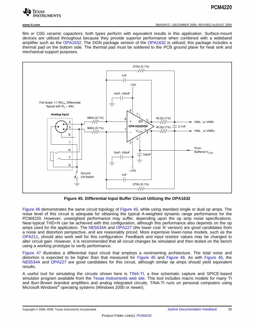
Figure 45 illustrates the input buffer/filter circuit utilized on the PCM4222EVM evaluation module, where thePCM4222 analog input section is identical to the PCM4220. This circuit has been optimized for measurementpurposes, so that it does not degrade the dynamic characteristics of the PCM4220. The resistors are primarily0.1% metal film. The 40.2Ω resistor is 1% tolerance thick film. The 1nF and 2.7nF capacitors may be either PPS
24 Submit Documentation Feedback Copyright © 2006–2009, Texas Instruments Incorporated
Product Folder Link(s): PCM4220
560 (0.1%)W
2
3
G
1
R
T
S
40.2 (1%)W
40.2 (1%)W
270 (0.1%)W
270 (0.1%)W
OPA1632DGN
Analog Input
Full-Scale: 11.76V DifferentialPP
Typical with R = 40WS
1nF
1nF
560 (0.1%)W
Ground
Lift Switch
2.7nF
10nF 100nF-
-15V
2
1
8EN
VOCM
VINL or VINR- -
VINL or VINR++
From
Buffered VCOM
7
6
3
4
5
10nF 100nF-
+15V
100nF
PCM4220
www.ti.com............................................................................................................................................. SBAS407C–DECEMBER 2006–REVISED AUGUST 2009
film or C0G ceramic capacitors; both types perform with equivalent results in this application. Surface-mountdevices are utilized throughout because they provide superior performance when combined with a widebandamplifier such as the OPA1632. The DGN package version of the OPA1632 is utilized; this package includes athermal pad on the bottom side. The thermal pad must be soldered to the PCB ground plane for heat sink andmechanical support purposes.
Figure 45. Differential Input Buffer Circuit Utilizing the OPA1632
Figure 46 demonstrates the same circuit topology of Figure 45, while using standard single or dual op amps. Thenoise level of this circuit is adequate for obtaining the typical A-weighted dynamic range performance for thePCM4220. However, unweighted performance may suffer, depending upon the op amp noise specifications.Near-typical THD+N can be achieved with this configuration, although this performance also depends on the opamps used for the application. The NE5534A and OPA227 (the lower cost 'A' version) are good candidates froma noise and distortion perspective, and are reasonably priced. More expensive lower-noise models, such as theOPA211, should also work well for this configuration. Feedback and input resistor values may be changed toalter circuit gain. However, it is recommended that all circuit changes be simulated and then tested on the benchusing a working prototype to verify performance.
Figure 47 illustrates a differential input circuit that employs a noninverting architecture. The total noise anddistortion is expected to be higher than that measured for Figure 45 and Figure 46. As with Figure 46, theNE5534A and OPA227 are good candidates for this circuit, although similar op amps should yield equivalentresults.
A useful tool for simulating the circuits shown here is TINA-TI, a free schematic capture and SPICE-basedsimulator program available from the Texas Instruments web site. This tool includes macro models for many TIand Burr-Brown branded amplifiers and analog integrated circuits. TINA-TI runs on personal computers usingMicrosoft Windows® operating systems (Windows 2000 or newer).
Copyright © 2006–2009, Texas Instruments Incorporated Submit Documentation Feedback 25
Product Folder Link(s): PCM4220

560W
40.2W
40.2W
270W
270W
1nF
1nF
100nF
VINL or VINR- -
VINL or VINR++
C1
+
+
560W
C2 U2
2.7nF
U1
VCOML
or
VCOMR
INPUT+
INPUT-
U1, U2 = NE5534A, OPA227, or similar
R W1
10kW
10kW
40.2W
40.2W
1.5kW
1.5kW
1nF
1nF
VINL ++ or VINR
VINL -- or VINR
C1
+
+
R W2C
2
U2
2.7nF
U3
U1
INPUT+
INPUT-
VCOML
or
VCOMR
U1, U2 = NE5534A, OPA227, or similar.
U3 = OPA227 or equivalent.
PCM4220
SBAS407C–DECEMBER 2006–REVISED AUGUST 2009............................................................................................................................................. www.ti.com
NOTE: C1 and C2 provide ac coupling. They may be removed if the dc offset from the circuit is negligible.
Figure 46. Alternative Buffer Circuit Using Standard Op Amps
NOTE: R1 and R2 are optional. When used, values may be selected for the desired attenuation.NOTE: C1 and C2 provide ac coupling. They may be removed if the dc offset from the circuit is negligible.
Figure 47. Noninverting Differential Input Buffer Utilizing Standard Op Amps
26 Submit Documentation Feedback Copyright © 2006–2009, Texas Instruments Incorporated
Product Folder Link(s): PCM4220

INTERFACING TO DIGITAL AUDIO TRANSMITTERS (AES3, IEC60958-3, and S/PDIF)
PCM4220
Divided by 2
FS1
LO
LO
HI
HI
FS0
LO
HI
LO
HI
Mode
Normal
Double Speed
Quad Speed
Reserved
MCKI BCK
LRCK
FS1
FS0
MCLK
CLK0
CLK1
512f (Normal)S
256f (Double Speed)S
128f (Quad Speed)S
DIT4192
Master
Clock
DATA
S/M
SCLK
SYNC
SDATA
M/S
LO = ADC Master
HI = ADC Slave
CLK1
LO
LO
HI
HI
CLK0
LO
HI
LO
HI
Mode
Quad Speed
Double Speed
Reserved
Normal
PCM4220
www.ti.com............................................................................................................................................. SBAS407C–DECEMBER 2006–REVISED AUGUST 2009
The serial output of audio analog-to-digital converters is oftentimes interfaced to transmitter devices that encodethe serial output data to either the AES3 or IEC60958-3 (or S/PDIF) interface formats. Texas Instrumentsmanufactures several devices that perform this encoding, including the DIT4192, DIX4192, SRC4382, andSRC4392. This section describes and illustrates the audio serial port interface connections required forcommunications between the PCM4220 and these devices. Register programming details for the DIX4192 andSRC4382/4392 are also provided.
Figure 48 shows the interface between a PCM4220 and a DIT4192 transmitter. This configuration supportssampling frequencies and encoded frame rates from 8kHz to 216kHz. For this example, the audio data formatmust be either Left-Justified or I2S; TDM formats are not supported by the DIT4192. In addition, the PCM4220VDD supply and DIT4192 VIO supply must be the same voltage, to ensure logic level compatibility.
Figure 49 illustrates the audio serial port interface between the PCM4220 and either a DIX4192 transceiver orSRC4382/SRC4392 combo sample rate converter/transceiver device. Port A of the DIX4192 orSRC4382/SRC4392 is utilized for this example. Data acquired by Port A are sent on to the DIT function blockwithin the interface device for AES3 encoding and transmission.
The DIX4192 and SRC4382/SRC4392 are software-configurable, with control register and data buffer settingsthat determine the operation of internal function blocks. Table 8 and Table 9 summarize the control registersettings for the Port A and the DIT function blocks for both A/D Converter Master and Slave modes, respectively.Input sampling and encoded frame rates from 8kHz to 216kHz are supported with the appropriate registersettings.
Figure 48. Interfacing the PCM4220 to a DIT4192
Copyright © 2006–2009, Texas Instruments Incorporated Submit Documentation Feedback 27
Product Folder Link(s): PCM4220

PCM4220
Divided by 2
MCKI
BCK
LRCK
DIX4192
or
SRC4392
512f (Normal)S
256f (Double Speed)S
128f (Quad Speed)S
Master
Clock
MCLK
DATA
BCKA
LRCKA
SDINA
PCM4220
SBAS407C–DECEMBER 2006–REVISED AUGUST 2009............................................................................................................................................. www.ti.com
NOTE: VDDPCM4220 = VIODIX4192 or SRC4392.Audio data format if I2S or Left Justified.Interface supports ADC Slave or Master configurations, depending on DIX4192, SRC4382, or SRC4392 register setup.
Figure 49. Interfacing the PCM4220 to a DIX4192, SRC4382, or SRC4392
Table 8. Register Configuration Sequence for an ADC Master Mode InterfaceREGISTER ADDRESS (hex) REGISTER DATA (hex) COMMENTS
7F 00 Select Register Page 000 Port A is Slave mode with Left-Justified audio data format, or03 01 Port A is Slave mode with I2S Data format
04 00 Default for Port A Slave mode operation64 Divide MCLK by 512 for Normal sampling, or
07 24 Divide MCLK by 256 for Double Speed Sampling, or04 Divide MCLK by 128 for Quad Speed sampling
08 00 Line Driver and AESOUT buffer enabledData buffers on Register Page 2 are the source for the DIT channel09 01 status (C) and user (U) data
01 34 Power up Port A and the DIT
Table 9. Register Configuration Sequence for an ADC Slave Mode InterfaceREGISTER ADDRESS (hex) REGISTER DATA (hex) COMMENTS
7F 00 Select Register Page 008 Port A is Master mode with Left-Justified audio data format, or03 09 Port A is Master mode with I2S Data format03 Divide MCLK by 512 for Normal sampling, or
04 01 Divide MCLK by 256 for Double Speed sampling, or00 Divide MCLK by 128 for Quad Speed sampling64 Divide MCLK by 512 for Normal sampling, or
07 24 Divide MCLK by 256 for Double Speed Sampling, or04 Divide MCLK by 128 for Quad Speed sampling
08 00 Line Driver and AESOUT buffer enabledData buffers on Register Page 2 are the source for the DIT channel09 01 status (C) and user (U) data
01 34 Power up Port A and the DIT
28 Submit Documentation Feedback Copyright © 2006–2009, Texas Instruments Incorporated
Product Folder Link(s): PCM4220

PCM4220
www.ti.com............................................................................................................................................. SBAS407C–DECEMBER 2006–REVISED AUGUST 2009
The DIT channel status (C) and user (U) data bits in register page 2 may be programmed after the DIT block haspowered up. To program these bits, disable buffer transfers by setting the BTD bit in control register 0x08 to '1'.Then, select register page 2 using register address 0x7F. You can now load the necessary C and U dataregisters for the intended application by writing the corresponding data buffer addresses. When you havefinished writing the C and U data, select register page 0 using register address 0x7F. Re-enable buffer transfersby setting the BTD bit in control register 0x08 to '0'.
Copyright © 2006–2009, Texas Instruments Incorporated Submit Documentation Feedback 29
Product Folder Link(s): PCM4220

PCM4220
SBAS407C–DECEMBER 2006–REVISED AUGUST 2009............................................................................................................................................. www.ti.com
Revision HistoryNOTE: Page numbers for previous revisions may differ from page numbers in the current version.
Changes from Revision B (October 2007) to Revision C ............................................................................................... Page
• Corrected statement concerning direction to drive PCMEN (pin 16) to disable PCM output .............................................. 18
Changes from Revision A (May 2007) to Revision B ...................................................................................................... Page
• Changed Figure 26 y-axis value from (dB) to (db/10,000) .................................................................................................. 12• Changed Figure 30 y-axis value from (dB) to (db/1000) ..................................................................................................... 13
30 Submit Documentation Feedback Copyright © 2006–2009, Texas Instruments Incorporated
Product Folder Link(s): PCM4220

PACKAGE OPTION ADDENDUM
www.ti.com 10-Dec-2020
Addendum-Page 1
PACKAGING INFORMATION
Orderable Device Status(1)
Package Type PackageDrawing
Pins PackageQty
Eco Plan(2)
Lead finish/Ball material
(6)
MSL Peak Temp(3)
Op Temp (°C) Device Marking(4/5)
Samples
PCM4220PFB ACTIVE TQFP PFB 48 250 RoHS & Green NIPDAU Level-3-260C-168 HR -40 to 85 PCM4220
PCM4220PFBR ACTIVE TQFP PFB 48 1000 RoHS & Green NIPDAU Level-3-260C-168 HR -40 to 85 PCM4220
(1) The marketing status values are defined as follows:ACTIVE: Product device recommended for new designs.LIFEBUY: TI has announced that the device will be discontinued, and a lifetime-buy period is in effect.NRND: Not recommended for new designs. Device is in production to support existing customers, but TI does not recommend using this part in a new design.PREVIEW: Device has been announced but is not in production. Samples may or may not be available.OBSOLETE: TI has discontinued the production of the device.
(2) RoHS: TI defines "RoHS" to mean semiconductor products that are compliant with the current EU RoHS requirements for all 10 RoHS substances, including the requirement that RoHS substancedo not exceed 0.1% by weight in homogeneous materials. Where designed to be soldered at high temperatures, "RoHS" products are suitable for use in specified lead-free processes. TI mayreference these types of products as "Pb-Free".RoHS Exempt: TI defines "RoHS Exempt" to mean products that contain lead but are compliant with EU RoHS pursuant to a specific EU RoHS exemption.Green: TI defines "Green" to mean the content of Chlorine (Cl) and Bromine (Br) based flame retardants meet JS709B low halogen requirements of <=1000ppm threshold. Antimony trioxide basedflame retardants must also meet the <=1000ppm threshold requirement.
(3) MSL, Peak Temp. - The Moisture Sensitivity Level rating according to the JEDEC industry standard classifications, and peak solder temperature.
(4) There may be additional marking, which relates to the logo, the lot trace code information, or the environmental category on the device.
(5) Multiple Device Markings will be inside parentheses. Only one Device Marking contained in parentheses and separated by a "~" will appear on a device. If a line is indented then it is a continuationof the previous line and the two combined represent the entire Device Marking for that device.
(6) Lead finish/Ball material - Orderable Devices may have multiple material finish options. Finish options are separated by a vertical ruled line. Lead finish/Ball material values may wrap to twolines if the finish value exceeds the maximum column width.
Important Information and Disclaimer:The information provided on this page represents TI's knowledge and belief as of the date that it is provided. TI bases its knowledge and belief on informationprovided by third parties, and makes no representation or warranty as to the accuracy of such information. Efforts are underway to better integrate information from third parties. TI has taken andcontinues to take reasonable steps to provide representative and accurate information but may not have conducted destructive testing or chemical analysis on incoming materials and chemicals.TI and TI suppliers consider certain information to be proprietary, and thus CAS numbers and other limited information may not be available for release.
In no event shall TI's liability arising out of such information exceed the total purchase price of the TI part(s) at issue in this document sold by TI to Customer on an annual basis.
PACKAGE OPTION ADDENDUM
www.ti.com 10-Dec-2020
Addendum-Page 2
TRAY
Chamfer on Tray corner indicates Pin 1 orientation of packed units.
*All dimensions are nominal
Device PackageName
PackageType
Pins SPQ Unit arraymatrix
Maxtemperature
(°C)
L (mm) W(mm)
K0(µm)
P1(mm)
CL(mm)
CW(mm)
PCM4220PFB PFB TQFP 48 250 10 x 25 150 315 135.9 7620 12.2 11.1 11.25
PACKAGE MATERIALS INFORMATION
www.ti.com 5-Jan-2022
Pack Materials-Page 1

MECHANICAL DATA
MTQF019A – JANUARY 1995 – REVISED JANUARY 1998
POST OFFICE BOX 655303 • DALLAS, TEXAS 75265
PFB (S-PQFP-G48) PLASTIC QUAD FLATPACK
4073176/B 10/96
Gage Plane
0,13 NOM
0,25
0,450,75
Seating Plane
0,05 MIN
0,170,27
24
25
13
12
SQ
36
37
7,206,80
48
1
5,50 TYP
SQ8,809,20
1,050,95
1,20 MAX0,08
0,50 M0,08
0°–7°
NOTES: A. All linear dimensions are in millimeters.B. This drawing is subject to change without notice.C. Falls within JEDEC MS-026


IMPORTANT NOTICE AND DISCLAIMERTI PROVIDES TECHNICAL AND RELIABILITY DATA (INCLUDING DATA SHEETS), DESIGN RESOURCES (INCLUDING REFERENCE DESIGNS), APPLICATION OR OTHER DESIGN ADVICE, WEB TOOLS, SAFETY INFORMATION, AND OTHER RESOURCES “AS IS” AND WITH ALL FAULTS, AND DISCLAIMS ALL WARRANTIES, EXPRESS AND IMPLIED, INCLUDING WITHOUT LIMITATION ANY IMPLIED WARRANTIES OF MERCHANTABILITY, FITNESS FOR A PARTICULAR PURPOSE OR NON-INFRINGEMENT OF THIRD PARTY INTELLECTUAL PROPERTY RIGHTS.These resources are intended for skilled developers designing with TI products. You are solely responsible for (1) selecting the appropriate TI products for your application, (2) designing, validating and testing your application, and (3) ensuring your application meets applicable standards, and any other safety, security, regulatory or other requirements.These resources are subject to change without notice. TI grants you permission to use these resources only for development of an application that uses the TI products described in the resource. Other reproduction and display of these resources is prohibited. No license is granted to any other TI intellectual property right or to any third party intellectual property right. TI disclaims responsibility for, and you will fully indemnify TI and its representatives against, any claims, damages, costs, losses, and liabilities arising out of your use of these resources.TI’s products are provided subject to TI’s Terms of Sale or other applicable terms available either on ti.com or provided in conjunction with such TI products. TI’s provision of these resources does not expand or otherwise alter TI’s applicable warranties or warranty disclaimers for TI products.TI objects to and rejects any additional or different terms you may have proposed. IMPORTANT NOTICE
Mailing Address: Texas Instruments, Post Office Box 655303, Dallas, Texas 75265Copyright © 2022, Texas Instruments Incorporated