High frequency isolationdual-active-bridge converter with ...
8
High frequency isolation dual-active-bridge converter with optimal control scheme based on solid-state transformer Liang Wang 1,a 1 Power Electronic & Motion Control Research Center, Shenzhen Graduate School of Harbin Institute of Technology, Shenzhen 518055, China , Zhiyun Bao 2 and Yi Wang 1 2 Shenzhen Polytechnic, Shenzhen 518055, China Abstract. This paper presents the design of high-frequency transformer isolation bidirectional DC/DC converter based on solid-state transformer (SST). A phase-shift dual-active-bridge (DAB) converter is employed to achieve high-frequency galvanic isolation, bidirectional power flow, and zero voltage switching of all switching devices, which leads to low switching losses with high frequency operation. Moreover, a master-slave control (MSC) strategy is designed for the DAB stage of SST system to reduce load on the controller and simplify modulation algorithm. The master controller executes all control and modulation calculations, and the slave controllers manage only device switching and protection. As the core circuit of SST system, DAB converter has wide applications such as battery energy storage device and hybrid electrical vehicles power system. Keywords: solid-state transformer; dual-active-bridge; master-slave control; simplify modulation algorithm. 1 Introduction The proliferation of distributed generation and renewable energy resources has motivated the researchers to investigate the feasibility of new microgrid operation mode Future Renewable Electric Energy Delivery and Management (FREEDM). The FREEDM system is a new medium-voltage microgrid composed of several solid-state transformers (SST), high-bandwidth digital communication, and distributed control. The future intelligent electric energy distribution and management systems are expected to integrate highly distributed and scalable renewable generationg sources. As the fundamental component of innovative smart microgrid system, SST is intended to replace the conventional bulky, heavy, and noisy low frequency (LF) transformers and performs the power flow control [1-2]. SST is a new power electronics system, can provide many additional advantages such as intelligent energy management, good power quality, low volum, reactive power compensation and high power density [3]. Fig. 1 shows the proposed SST based on the dual active bridge (DAB) converter and cascaded H- bridge multilevel inverter (CHMI). The SST includes a DAB DC/DC stage to step up the 400Vdc link to the high voltage dc link, a cascade H-Bridge multilevel DC/AC inverter stage to provide active power and reactive power for the 10kV-ac grid. As the core device of SST system, high frequency a Corresponding author: [email protected] International Conference on Advanced Electronic Science and Technology (AEST 2016) © 2016. The authors - Published by Atlantis Press 254
Transcript of High frequency isolationdual-active-bridge converter with ...
High frequency isolation dual-active-bridge converter with optimal control scheme based on solid-state transformer
Liang Wang1,a
1Power Electronic & Motion Control Research Center, Shenzhen Graduate School of Harbin Institute of Technology, Shenzhen 518055, China
, Zhiyun Bao2 and Yi Wang1
2Shenzhen Polytechnic, Shenzhen 518055, China
Abstract. This paper presents the design of high-frequency transformer isolation bidirectional DC/DC converter based on solid-state transformer (SST). A phase-shift dual-active-bridge (DAB) converter is employed to achieve high-frequency galvanic isolation, bidirectional power flow, and zero voltage switching of all switching devices, which leads to low switching losses with high frequency operation. Moreover, a master-slave control (MSC) strategy is designed for the DAB stage of SST system to reduce load on the controller and simplify modulation algorithm. The master controller executes all control and modulation calculations, and the slave controllers manage only device switching and protection. As the core circuit of SST system, DAB converter has wide applications such as battery energy storage device and hybrid electrical vehicles power system. Keywords: solid-state transformer; dual-active-bridge; master-slave control; simplify modulation algorithm.
1 Introduction The proliferation of distributed generation and renewable energy resources has motivated the researchers to investigate the feasibility of new microgrid operation mode Future Renewable Electric Energy Delivery and Management (FREEDM). The FREEDM system is a new medium-voltage microgrid composed of several solid-state transformers (SST), high-bandwidth digital communication, and distributed control. The future intelligent electric energy distribution and management systems are expected to integrate highly distributed and scalable renewable generationg sources. As the fundamental component of innovative smart microgrid system, SST is intended to replace the conventional bulky, heavy, and noisy low frequency (LF) transformers and performs the power flow control [1-2]. SST is a new power electronics system, can provide many additional advantages such as intelligent energy management, good power quality, low volum, reactive power compensation and high power density [3].
Fig. 1 shows the proposed SST based on the dual active bridge (DAB) converter and cascaded H-bridge multilevel inverter (CHMI). The SST includes a DAB DC/DC stage to step up the 400Vdc link to the high voltage dc link, a cascade H-Bridge multilevel DC/AC inverter stage to provide active power and reactive power for the 10kV-ac grid. As the core device of SST system, high frequency
a Corresponding author: [email protected]
International Conference on Advanced Electronic Science and Technology (AEST 2016)
© 2016. The authors - Published by Atlantis Press 254

AEST2016
isolation (HFI) DAB converter are attracting more and more attentions for high power density, reduced weight, and low noise without compromising efficiency, cost, and reliability [4-5].
B
C
O
A
DABCHMI
vao
DC-Bus
DC-Busisc
Rsc Rsa
isa
isb
Rsb
Cs
220V
-AC
DC/DC
400V DC Bus
Nvsavsbvsc
LsaLsc Lsb Ls
Ls
Li-lonPV
DC/AC
FID
FID
FID
380V
-AC
Ls
Ls
Ls
DC/AC
AC/DC
LV
AC
#1
#2
#3
N
va vb vc
N A B C
HVDC
HVDC
HVDC
10kVAC
Figure 1. Topology of the proposed three- phase SST.
2 Dual-active-bridge topology analyses Generally, under the same rated voltage and current of switches conditions, the transmission power of converter is proportional to the switches number. Such as the power capacity of four switches is double that of dual-switch, but half that of eight switches, in this case, the dual active bridge is the biggest power capacity. Meanwhile, the filter of DAB is smaller with the same output power than others. In addition, the DAB has the advantages of ease of realizing soft-switching, bidirectional power transfer capability, and modular and symmetric structure, etc. Thus, DAB has been served as the core circuit for the solid state transformer system [6-8].
Fig. 2 shows the topology of DAB, which composes of two H-bridge, two dc link capacitors, an auxiliary inductor, and an HFI transformer. The HFI transformer provides the required galvanic isolation and voltage matching between two voltage levels. The inductor serves as the instantaneous energy storage device.
The transferred power of DAB by phase-shift can be expressed as:
2
(V / 2)(V / 2)( )2
dcH dcLout
nP
fLπ θ θ
π−
= (1)
Where, L is the HF transformer leakage inductance, VdcH is the high voltage dc-link, VdcL is the 400V dc-link and is the phase-shift angle. In addition, the output current can be given by :
2
( )8
dcLoutout
dcH
nVPIV fL
π θ θπ
−= = (2)
255

AEST2016
driving signal
g1, g2...g8
S1
S3
S2
S4
Q1 Q2
Q3 Q4
vpiL vs
input voltage and current signal
output voltage and current signal
DSP-controllersoft start & protection
H1-bridge H2-bridge
LsA
BC
D
Figure 2. DAB topology and control method.
Based on above, the timing diagram of DAB with single phase-shift control is shown in Fig. 3. The phase-shift angle is adjusted between primary and secondary side, whose range is from 0 to π. The primary and secondary voltage, VAB and VCD, can be controlled by the angle [9].
t0 t1 t2 t3t4 t5 t6 t7 t8t9t10
S1&S4
Q2&Q3
vAB
vL
iL
i1
vCD
1 2 3 4 5 6 7 8 9 10
S2&S3
Q1&Q4
Figure 3. Voltage and current waveforms of DAB control.
256

AEST2016
3 The DAB control scheme optimization based on SST system Fig. 4 shows control architecture of the DAB stage with two different methods. The DAB stage steps up the 400V dc link to 4kV dc output which is fed to CHMI stage. The DAB stage consists of 9 DAB modules, if the independent control is used (as shown in Fig. 4a), which will include 9 control loops, resulting in increasing pressure to the software operation and affect the reliability of the system. In contrast, in the proposed control circuit only one DAB converter is utilized as the master PI (proportional-Integral) voltage controller, which executes all control and modulation calculations and sends the resultant converter driving command signals to other DAB slave controllers via high speed fiber-optic (as shown in Fig. 4b).
DAB #1
Power flow
driver signal
Phase A Phase B Phase C
Feedback signal input: 400Voutput: HVDC
To CHMI #1
400V
400V
400V
400V
DAB #2
DAB #3
DAB #2
DAB #3
DAB #1
DAB #2
DAB #3
controller#2
controller#1
controller#3
To CHMI #2
To CHMI #3
DAB #1
Feedback signal
driver signal
driver signal
(a) Independent controller
DAB #1
Power flow
mastercontroller
optical
drivingsignal
Phase A Phase B Phase C
Feedback signalinput: 400V
output: HVDC
400V
400V
400V
400V
slavecontroller
slavecontroller
drivingsignal
drivingsignal
DAB #2
DAB #3
DAB #1
DAB #2
DAB #3
DAB #1
DAB #2
DAB #3
driving signal
HVDC
HVDC
HVDC
CHMI 1
CHMI 2
CHMI 3
(b) Master-salve controller
Figure 4. The architecture of the DAB stage with two different control strategy.
Typically, 8 DAB slave controllers only manage devices switching and protection. Also to calculate the power transferred by each module and implement the protection of over-voltage and over-current, the voltage and current of input-side and output-side are all sensed. Since 9 circuit structures are completely identical, the output voltage amplitude of each DAB converter should be equal to the reference voltage with the same driving signals assuming that the components (switches
257

AEST2016
and transformers) of each DAB stage are ideal. Therefore, the proposed master-slave controller in the DAB stage not only provides the high frequency galvanic isolation, but also simplifies the complex algorithm and improves the dynamic performance.
4 The simulation and experimental verification
To verify the proposed DAB controller simulation prototype of Fig. 2 is implemented using Matlab/Simulink. The simulation parameters are listed in Table I.
Table 1. Parameters of the simulation system
Basic Parameters Value
Input DC Voltage 400V
Output DC Voltage 400V
Switching Device Frequency 100kHz
Output power rate 2.5kW
Leakage inductance 5.5uH
DC capacitor (HV/LV) 5mF/5mF
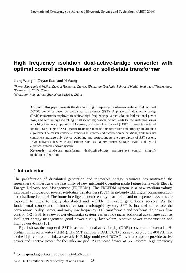
As shown in Fig. 5, the basic transmission power characterization of DAB with a single phase-shift control is implemented, where D= /π is the phase-shift ratio. Fig. 5 (a) and (b) show the relation curve of transferred power and the phase-shift ratio D. It can be seen that the transmission power of DAB can be accommodated by D. The transmission current and power increase in the condition of 0 0.5D≤ ≤ , and the power decreases in the condition of 0.5 1D≤ ≤ . From Fig. 5(c), the transmission power is symmetric at the median axis D=0.5, and the maximum point of the transmission power is achieved at D=0.5. Furthermore, the power is transferred from high voltage dc-link to 400V dc-link in the condition of 1 0D− ≤ ≤ .
0 1 2 3 4 5 6Time(5us/div)
VAB
VCD
iL
0400
-400
0400
-400
10505
10(A)
(V)
(V)
(a)
258
AEST2016
VAB
VCD
iL
0 1 2 3 4 5 6Time(5us/div)
0400
-400
0400
-400
200
40
-20-40
(V)
(V)
(A)
(b)
k=1.5k=1k=0.5
P out
(p
.u.)
(c)
Figure 5. The curve of phase-shift ratio and output power
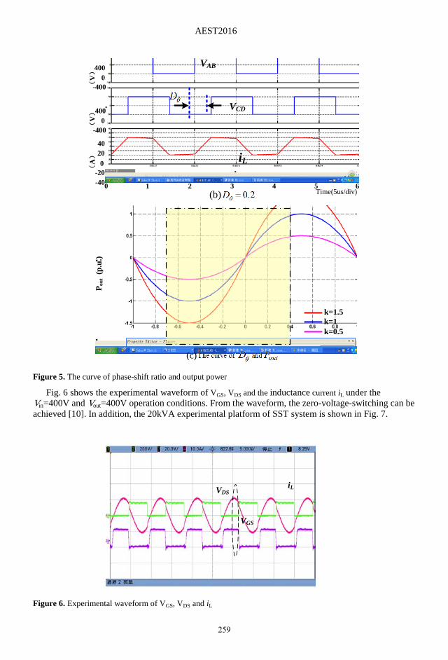
Fig. 6 shows the experimental waveform of VGS, VDS and the inductance current iL under the Vin=400V and Vout=400V operation conditions. From the waveform, the zero-voltage-switching can be achieved [10]. In addition, the 20kVA experimental platform of SST system is shown in Fig. 7.
VDS
VGS
iL
Figure 6. Experimental waveform of VGS, VDS and iL
259

AEST2016
Figure 7. The experimental platform of SST system
5 Conclusion
This paper analysis starts from the detailed architecture of solid state transformer, which mainly includes the bidirectional DC/DC converter and the cascaded H-Bridge multilevel inverter. As the core part of the SST system, this paper focused on the master-slave control strategy on the DAB stage. In the proposed control circuit only one DAB converter is utilized as the master controller, which executes all control and modulation calculations and sends the resultant converter driving command signals to other DAB slave controllers via high speed fiber-optic. The proposed control scheme can simplify the algorithm complexity, improving the operation reliability, expecting to provide theory reference and technology supports for the further SST system development.
Acknowledgements This work was supported by the Shenzhen Science and Technology Plan Project (Grant No.: JSGG20140519171924378 and JCYJ20140417172417127).
References 1. J. Carrasco, L. Franquelo, et al. Power-electronic systems for the grid integration of renewable
energy sources: A survey. IEEE Trans. Ind. Electron., 53, 4, 1002–1016(2006). 2. H. Fan and H. Li. High frequency high efficiency bidirectional DC–DC converter module design
for 10 kVA solid state transformer,” in Proc. IEEE Appl. Power Electron. Conf., 210–215(2010). 3. B. Zhao, Q. Song, et al. Overview of dual active bridge isolated bidirectional dc-dc converter for
high frequency link power convertersion system. IEEE Trans. Power Electron., 29, 16, 4091-4106 (2014).
4. J. Lee, Y. Jeong, B. Han. A two stage isolated/bidirecional dc/dc converter with current ripple reduction technique. IEEE Trans. Ind Electron., 59, 3, 644-646(2012).
5. S. Inoue and H. Akagi. A bidirectional dc-dc converter for an energy storage system with galvanic isolation. IEEE Trans. Power Electron., 22, 6, 2299–2306(2007).
6. T. Zhao, G. Wang, et al. Voltage and power balance control for a cascaded h-bridge converter based solid state transformer. IEEE Trans. Power Electron., 28, 10, 1523-1532(2013).
260

AEST2016
7. A. Kadavelugu, S. Baek, et aI. High-frequency design considerations of dual active bridge 1200V SiC MOSFET dc-dc converter. 261h Annual IEEE Applied Power Electronics Conference and Exposition. (APEC), 314-320(2011).
8. Y. Xie, J. Sun, et aI. Power flow characterization of a bidirectional galvanically isolated high-power dc/dc converter over a wide operating rang. IEEE Trans. Power Electron., 25, 1, 54–66(2010).
9. H. Fan, H. Li. High frequency transformer isolated bidirectional dc-dc converter modules with high efficiency over wide load range for 20kVA solid state transformer. IEEE Trans. Power Electron., 26, 10, 3599-3608(2011).
10. H.Tao, A.Kotsopoulos, et aI. Transformer-coupled multiport ZVS bidirectional dc-dc converter with wide input range. IEEE Trans. Power Electron., 23, 2, 771–781(2008).
261