High Efficiency Single Phase Inverter Design
5
High Efficiency Single Phase Inverter Design Didi Istardi Electric Machine Control Laboratory, Electrical Engineering Departement Politeknik Negeri Batam, Indonesia [email protected] Basyir Halim, Arif Juwito Febriansyah Mechantronics Study Program Electrical Engineering Departement Politeknik Negeri Batam, Indonesia Abstract—The solar power plant is one of the renewable energy that already was implemented in around the world. The important component in the renewable power plant is inverter device that convert the direct current to alternating current. The problem in the inverter are power quality, harmonics, and grid system. This paper introduced design inverter single phase with totem pole circuit. The circuit reduces losses in inverter. Besides that, DC link in PCB, component placement configuration, and adding filter in the output of inverter was implemented in the design. The result shown that the inverter have optimum efficiency at 98.67% and have a small total harmonics distortion with LC load. Keywords—totem pole, inverter, DC link, filter I. INTRODUCTION Renewable energy is the most important energy resource in Small Island that do not connect to power system grid. There are some alternatives renewable energy that can be used in that area such as solar, wind, tidal, and micro hydro. The solar power plant is the easiest, availability, and low maintenance [1]. The main components of solar power plant are photovoltaic (PV) cells, controller, battery, and inverter. The PV cells convert solar energy to electric energy that have many different cell configurations. The controller is the brain of the solar power plant that can manage and control the energy from the PV cells to the load and also from and to battery. The battery is the storage energy that can charge and discharge conveniently through controller. The inverter is consisting of power electronics components that can convert direct current (DC) to DC and DC to alternating current (AC). One of development in the solar power plant technology is the inverter design for solar power plant. The inverter must have a high efficiency and can be stand alone or connect to the grid [2]-[3]. The basic design of inverter can be seen in Fig. 1. The T1-T4 are solid state components that act like switching device. The solid state component that be used in inverter are transistor, IGBT, MOSFET, or SCR. The output of the inverter is AC voltage with zero DC component. Therefore, it still contain harmonics. The low pass filter is installed in the inverter output to reduce the high frequency harmonics. This harmonics cause some problem in output inverter such as power quality, degradation of equipment, and sinusoidal waveform quality. Moreover, the output inverter must can match with grid system, V DC T1 T4 T3 T2 + V O - D1 D2 D3 D4 I O Figure 1. Basic configuration of DC to AC Inverter According to that issue, there are some research about single phase inverter design was done by [4], [5], [6], and [7]. The drive circuit and control are common problem that appear in inverter. The output of inverter must have good characteristics and can match with the grid. The brain of single phase inverter are microcontroller as main controller with different technique. The improved DC-AC converter was use opto-coupler as connector between controller and solid state component [8], [9], and [10]. Therefore, the losses in this opto- coupler was identified and must to reduce in order to have a good efficiency and reliable design. The losses in this part can be reduced by design in good grounding and DC link connection [8]. The inverter design in [4]-[9] are still have power quality problem and control technique problem. In practical, there are a dead time that is required to avoid shoot-through faults; short circuit across the DC rail. The dead time creates low frequency envelope that make low frequency harmonics emerged. This is the main source of distortion for high quality sine wave inverter. Therefore, the inverter design by [6] and [7] was be combined to have a good quality power. In this paper, the design of totem pole inverter is proposed for reduced losses and improve stability. The PWM was generated by Arduino microcontroller with short delay. The paper is organized as follows: In the next section, a brief review of propose design of Totem Pole Inverter are presented. In Section III presents implementation of Totem Pole Inverter and discussion of the results. Finally, the conclusions are made in section IV. II. PROPOSE DESIGN OF TOTEM POLE INVERTER Inverter is an electronic device that is used to convert the direct signal into alternating signal. The output of the inverter can be either an AC voltage with sine wave form (sine wave), a square wave (square wave), or sine modification (Modified Sine Wave). Semiconductor devices that are widely used in the Proc. EECSI 2017, Yogyakarta, Indonesia, 19-21 September 2017 978-1-5386-0549-3/17/$31.00 ©2017 IEEE . 353
Transcript of High Efficiency Single Phase Inverter Design

High Efficiency Single Phase Inverter Design
Didi Istardi Electric Machine Control Laboratory, Electrical Engineering Departement Politeknik Negeri Batam, Indonesia
Basyir Halim, Arif Juwito Febriansyah Mechantronics Study Program
Electrical Engineering Departement Politeknik Negeri Batam, Indonesia
Abstract—The solar power plant is one of the renewable energy that already was implemented in around the world. The important component in the renewable power plant is inverter device that convert the direct current to alternating current. The problem in the inverter are power quality, harmonics, and grid system. This paper introduced design inverter single phase with totem pole circuit. The circuit reduces losses in inverter. Besides that, DC link in PCB, component placement configuration, and adding filter in the output of inverter was implemented in the design. The result shown that the inverter have optimum efficiency at 98.67% and have a small total harmonics distortion with LC load.
Keywords—totem pole, inverter, DC link, filter
I. INTRODUCTION
Renewable energy is the most important energy resource in Small Island that do not connect to power system grid. There are some alternatives renewable energy that can be used in that area such as solar, wind, tidal, and micro hydro. The solar power plant is the easiest, availability, and low maintenance [1]. The main components of solar power plant are photovoltaic (PV) cells, controller, battery, and inverter. The PV cells convert solar energy to electric energy that have many different cell configurations. The controller is the brain of the solar power plant that can manage and control the energy from the PV cells to the load and also from and to battery. The battery is the storage energy that can charge and discharge conveniently through controller. The inverter is consisting of power electronics components that can convert direct current (DC) to DC and DC to alternating current (AC).
One of development in the solar power plant technology is the inverter design for solar power plant. The inverter must have a high efficiency and can be stand alone or connect to the grid [2]-[3]. The basic design of inverter can be seen in Fig. 1. The T1-T4 are solid state components that act like switching device. The solid state component that be used in inverter are transistor, IGBT, MOSFET, or SCR. The output of the inverter is AC voltage with zero DC component. Therefore, it still contain harmonics. The low pass filter is installed in the inverter output to reduce the high frequency harmonics. This harmonics cause some problem in output inverter such as power quality, degradation of equipment, and sinusoidal waveform quality. Moreover, the output inverter must can match with grid system,
VDC
T1
T4
T3
T2
+ VO -
D1
D2
D3
D4
IO
Figure 1. Basic configuration of DC to AC Inverter
According to that issue, there are some research about single phase inverter design was done by [4], [5], [6], and [7]. The drive circuit and control are common problem that appear in inverter. The output of inverter must have good characteristics and can match with the grid. The brain of single phase inverter are microcontroller as main controller with different technique. The improved DC-AC converter was use opto-coupler as connector between controller and solid state component [8], [9], and [10]. Therefore, the losses in this opto-coupler was identified and must to reduce in order to have a good efficiency and reliable design. The losses in this part can be reduced by design in good grounding and DC link connection [8].
The inverter design in [4]-[9] are still have power quality problem and control technique problem. In practical, there are a dead time that is required to avoid shoot-through faults; short circuit across the DC rail. The dead time creates low frequency envelope that make low frequency harmonics emerged. This is the main source of distortion for high quality sine wave inverter. Therefore, the inverter design by [6] and [7] was be combined to have a good quality power.
In this paper, the design of totem pole inverter is proposed for reduced losses and improve stability. The PWM was generated by Arduino microcontroller with short delay. The paper is organized as follows: In the next section, a brief review of propose design of Totem Pole Inverter are presented. In Section III presents implementation of Totem Pole Inverter and discussion of the results. Finally, the conclusions are made in section IV.
II. PROPOSE DESIGN OF TOTEM POLE INVERTER
Inverter is an electronic device that is used to convert the direct signal into alternating signal. The output of the inverter can be either an AC voltage with sine wave form (sine wave), a square wave (square wave), or sine modification (Modified Sine Wave). Semiconductor devices that are widely used in the
Proc. EECSI 2017, Yogyakarta, Indonesia, 19-21 September 2017
978-1-5386-0549-3/17/$31.00 ©2017 IEEE .353

power inverter are MOSFET, IGBT, Transistor, or Thyristor. There are two types of output signal can be generated by the inverter for solar plant. Firstly, the low and medium power application can be used square wave output signal. Secondly, high power application be used sine waves output signal.
The proposed inverter technique used in this paper based on standard single phase inverter. The design diagram of proposed inverter was shown in Fig.2.
Solid state drives Power Electronic Converter LC Filter output
Energy ManagementCharging Battery Controller
Figure 2. The proposed Inverter Diagram
From Fig.2 can be seen that the battery management system have responsible to control and manage the current in the systems. The inverter was change the 16 Vdc to 220 Vac sinusoidal that can be explained in next sub section. This part uses microcontroller as brain of the system. An LC section low-pass filter is normally fitted at the inverter output to reduce the high frequency harmonics.
A. Opto Coupler
This circuit uses optocoupler that have continues fast switching and easy to activate with a small voltage of 1 volt - 1.3 volt. Another function of this opto coupler is to protect from feedback current from the load to controller. In this paper uses TLP 521 component as optocoupler that can be seen in Fig. 3
Figure 3. Basic opto-couple circuit
In Fig. shows that there are 4 opto-coupler in the circuit. The opto-coupler connect to each solid state component. The resistor uses to limit the current in signal.
B. Totem Pole circuit
This circuit can be used to reduce power loss in the systems at high frequency switching. The solid state component can be more reliable with this circuit. The current at gate MOSFET can be released as fast as switching frequency. The switching losses at the solid state can be calculated [5]
( ) ( )( )1
,,2
cos82
12,
cos38
1
6
++
++
+
=
swofft
swont
swf
QI
QV
CEV
QI
MQ
IonCE
RM
QP
θπ
θπ
where M : Modulation index (0<M<1) VCE : collector-emitter voltage [V] RCE : strain drain to source on-resistance [Ω]
IQ : Current in MOSFET [A] fsw : frequency switching [Hz]
From equation (1), the switching losses depend on rise time and fall time of the semiconductor component. With the totem pole circuit, the fall time in switching period is faster than without it. In this circuit use PNP and NPN transistor in series that can be shown in Fig. 4.
Figure 4. Totem Pole circuit of Inverter
From Fig.3, the PNP and NPN transistor can deleiver signal to semiconductor devices in two legs. The first and the second leg is delayed by 1800. The current limited by resistor 1K.
C. Logical circuit
The purpose of this circuit is to invert signal due to the microcontroller that was used in this system. It was invert from high signal to low signal and vice versa. The circuit can be seen in Fig. 5.
Proc. EECSI 2017, Yogyakarta, Indonesia, 19-21 September 2017
354

Figure 5. Not Logical Circuit of Inverter
D. Inverting Circuit
This circuit serves to change the input DC voltage to AC output voltage. The DC-to-AC H-Bridge circuit comprises four MOSFETs, coupled as H-bridge 2 P-channel MOSFETs for positive voltage (+), and 2 M-type N-channel MOSFETs for negative voltage (-). It also comes with pull-up, pull-down and activated circuit through optocoupler that is triggered from microcontroller.
The working principle of this circuit when Q1 and Q4 active at the same time then the output connector issued a positive voltage of +16 volts and when Q2 and Q3 active simultaneously then the output connector issued a negative voltage of -16 volts, so with a fast switching can produce AC voltage 16 volt. And the voltage is inputted to the step-up transformer. Schematic circuit as shown in Fig. 6.
Figure 6. Inverter circuit
E. PWM Circuit
The PWM circuit that was be used in this paper is using Arduino Uno Microcontroller (based on ATmega Microcontroller). The frequency output is 50 Hz with reduced
ripple factor. The carrier frequency that be used is 1500 Hz. Therefore, the complete one cyles of sinusoidal output contains 30 impulses as shown in Fig. 7.
Figure 7. PWM output
F. Filter Design
Filter uses to improve the output of inverter. The inverter output signal without filter is manipulated using
( )2)(
)()(
sI
sOsY =
Where O(s) is sinusoidal signal in Laplace transform and I(s) is PWM signal in Laplace transform.
( )322
)(ω
ω
+=
ssO
By using Eq. (2) and (3),
( )
= −−−+=
59
0)4(
036.0sin31067.011
21067.0
22)(
i sxnxxes
nsxex
ssY
ω
ω
After simulation and calculation, the value of the filter that was be used in this circuit are 68 uF for capacitor and 10 mH for inductor with variable resistor. The circuit was protected by fuse 4 A to protect overload and short circuit conditions.
III. RESULT AND DISCUSSION
The proposed totem pole inverter is implemented for single phase solar panel application. The detail hardware design and its performance is evaluated and simulated in this sections. The hardware design consists two boards; controller board and inverter board. The controller board consists microcontroller to generate PWM signal and opto coupler circuit. The other consists totem poles, inverter, and filter circuit. The mechanical design can be seen in Fig. 8.
Proc. EECSI 2017, Yogyakarta, Indonesia, 19-21 September 2017
355
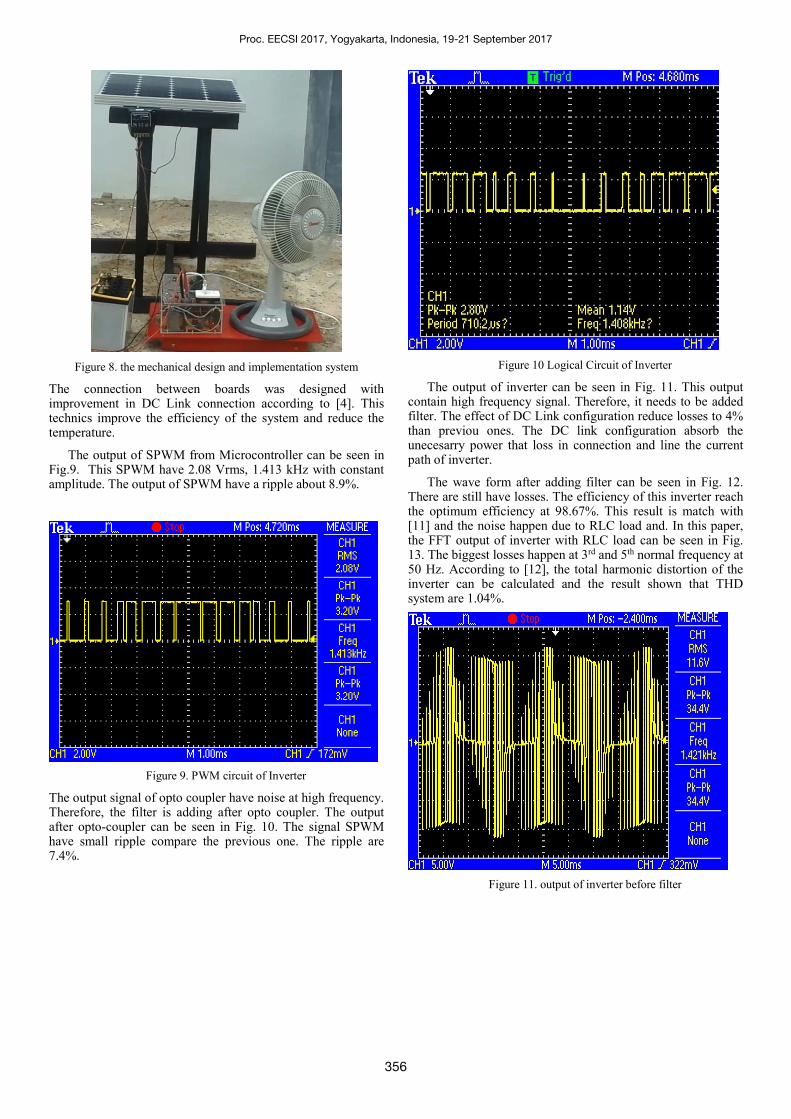
Figure 8. the mechanical design and implementation system
The connection between boards was designed with improvement in DC Link connection according to [4]. This technics improve the efficiency of the system and reduce the temperature.
The output of SPWM from Microcontroller can be seen in Fig.9. This SPWM have 2.08 Vrms, 1.413 kHz with constant amplitude. The output of SPWM have a ripple about 8.9%.
Figure 9. PWM circuit of Inverter
The output signal of opto coupler have noise at high frequency. Therefore, the filter is adding after opto coupler. The output after opto-coupler can be seen in Fig. 10. The signal SPWM have small ripple compare the previous one. The ripple are 7.4%.
Figure 10 Logical Circuit of Inverter
The output of inverter can be seen in Fig. 11. This output contain high frequency signal. Therefore, it needs to be added filter. The effect of DC Link configuration reduce losses to 4% than previou ones. The DC link configuration absorb the unecesarry power that loss in connection and line the current path of inverter.
The wave form after adding filter can be seen in Fig. 12. There are still have losses. The efficiency of this inverter reach the optimum efficiency at 98.67%. This result is match with [11] and the noise happen due to RLC load and. In this paper, the FFT output of inverter with RLC load can be seen in Fig. 13. The biggest losses happen at 3rd and 5th normal frequency at 50 Hz. According to [12], the total harmonic distortion of the inverter can be calculated and the result shown that THD system are 1.04%.
Figure 11. output of inverter before filter
Proc. EECSI 2017, Yogyakarta, Indonesia, 19-21 September 2017
356

Figure 12 Output of Inverter
Figure 13. FFT Output of Inverter
IV. CONCLUSION
The design of totem pole inverter single phase was implemented. There still have ripple in signal SPWM and also in H-Bridge converter. The result shown that the efficiency of the inverter is 98.67% with THD 1.04%. This THD match with IEEE standard in THD for power system.
ACKNOWLEDGMENT
Thanks to PT Lancang Kuning Perkasa for supporting this project, especially to Mr. Muslim Ansori.
REFERENCES
[1] Rafid Haidar, Rajin Alam, Nafise B.Y., Khosru M.S., “Design and
construction of single phase pure sine wave inverter for photovoltaic aplication”, IEEE/OSA/IAPR International Conference on Informatics, Electronics& Vision 2012, pp 190-194
[2] Xu Jun, Han Kailing, “The single phase inverter design for photovolataic systems”, 2016 International Symposium on Computer, Consumer, and Control, pp 341-344
[3] A. Ali Q., Awais Amin, Abdul Manan, M Khalid, “ Design and Implementation of Micocontroller Based PWM Technique For Sine Wave Inverter”, IEEE POWERENG Conference, pp 163-167, Lisbon 2009
[4] P. Sachis, I. Echeverria, A. Ursua, O. Alonso, E. Gubia, L. Marroyo,” Electronics Converter for the Analysis of Photovoltaic Arrays and Inverters”, IEEE 2003, pp. 1748-1753.
[5] Didi Istardi, Andy Triwinarko, “ Design of Snubber Circuit and PI Control to Achieve Load Independent Output Voltage in Micro Smart Home System’, 2014 International Conference on Smart-Green technology in Electrical nad Information Systems, pp. 7-12, Bali, Nov 2014.
[6] Ebrahim Babaei, Sara Laali, S. Alilu, “ Cascaded Multilevel Inverter with Series Connection of Novel H-Bridge Basic Unit’, IEEE Transaction on Industrial Electronics, Vol. 61, No. 12, pp. 6664-6671, December 2014.
[7] Quan Li, Peter Wolfs, “ A Review of the Single Phase Photovoltaic Module Integrated Converter Topologies with Three Different DC Link Configuration’, IEEE Transaction on Power Electronics, vol. 23, No.3, pp. 1320-1333, May 2008.
[8] Didi Istardi, “ Effect of Non-Tight Constructions of DC Link and Damping Oscillation to Improve the Effeciency of Fly-back Converter”, Proceeding of 3rd APTECS, pp. 201-406, ITS Surabaya, Dec 2011
[9] Boaming Ge, Yushan Liu, et el., “ An Active Filter Method to Eliminate DC-Side Low-Frequency Power for a Single-Phase Quasi-Z-Source Inverter’, IEEE Transaction on Power Electronics, vol. 63, No.8, pp. 4834-4848, August 2016.
[10] Yan Zhou, Hongbo Li, Hua Li, “ A Single Phase PV Quasi-Z-Source Inverter with Reduced Capacitance using Modified Modulation and Double Frequency Ripple Suppression Control’, IEEE Transaction on Power Electronics, vol. 31, No.3, pp. 2166-2173, March 2016
[11] Gua-Rong Zhu, H. Wang, B. Liang, A.C. Tan, J. Jiang, “ Enhanced Single-phase Full-Bridge Inverter with Minimal Low-Frequency Current Ripple”, IEEE Transaction on Industrial Electronics, vol. 63, No.2, pp. 937-943, Februari 2016.
[12] Brandon J. P., David J. P., “A Single Phase Photovoltaic Inverter Topology with a Series-connected Energy Buffer’, IEEE Transaction on Power Electronics, vol. 28, No.10, pp. 4603-4611, Oct. 2013
Proc. EECSI 2017, Yogyakarta, Indonesia, 19-21 September 2017
357