High-Definition Multimedia Interface (HDMI) IP Core User Guide...TMDS encoding is based on an 8-bit...
78
UG-HDMI 2017.05.08
Transcript of High-Definition Multimedia Interface (HDMI) IP Core User Guide...TMDS encoding is based on an 8-bit...

High-Definition Multimedia Interface(HDMI) IP Core User GuideUG-HDMI2017.05.08
Last updated for Intel® Quartus® Prime Design Suite: 17.0
SubscribeSend Feedback

Contents
1 HDMI Quick Reference..................................................................................................... 4
2 HDMI Overview................................................................................................................52.1 Resource Utilization................................................................................................ 9
3 HDMI Getting Started.....................................................................................................113.1 Installing and Licensing IP Cores............................................................................113.2 Specifying IP Core Parameters and Options.............................................................. 12
4 HDMI Source..................................................................................................................144.1 Source Functional Description.................................................................................14
4.1.1 Source TMDS/TERC4 Encoder..................................................................... 144.1.2 Source Video Resampler............................................................................ 154.1.3 Source Window of Opportunity Generator.....................................................204.1.4 Source Auxiliary Packet Encoder..................................................................204.1.5 Source Auxiliary Packet Generators............................................................. 224.1.6 Source Auxiliary Data Path Multiplexers....................................................... 224.1.7 Source Auxiliary Control Port...................................................................... 224.1.8 Source Audio Encoder................................................................................26
4.2 Source Interfaces................................................................................................. 284.3 Source Clock Tree................................................................................................. 30
5 HDMI Sink......................................................................................................................325.1 Sink Functional Description.................................................................................... 32
5.1.1 Sink Channel Word Alignment and Deskew................................................... 325.1.2 Sink TMDS/TERC4 Decoder........................................................................ 345.1.3 Sink Video Resampler................................................................................355.1.4 Sink Auxiliary Decoder...............................................................................355.1.5 Sink Auxiliary Packet Capture..................................................................... 375.1.6 Sink Auxiliary Data Port............................................................................. 395.1.7 Sink Audio Decoding..................................................................................41
5.2 Sink Interfaces..................................................................................................... 445.2.1 Avalon-MM SCDC Management Interface......................................................475.2.2 Status and Control Data Channel Interface................................................... 47
5.3 Sink Clock Tree.....................................................................................................47
6 HDMI Parameters.......................................................................................................... 496.1 HDMI Source Parameters....................................................................................... 496.2 HDMI Sink Parameters...........................................................................................496.3 HDMI Design Example Parameters.......................................................................... 50
7 HDMI Hardware Demonstration..................................................................................... 527.1 Hardware Demonstration Components..................................................................... 52
7.1.1 Transceiver Native PHY (RX)....................................................................... 557.1.2 Altera PLL IP Cores....................................................................................587.1.3 Altera PLL Reconfig IP Core........................................................................ 607.1.4 Multirate Reconfig Controller (RX)............................................................... 607.1.5 Oversampler (RX)..................................................................................... 617.1.6 DCFIFO................................................................................................... 62
Contents
High-Definition Multimedia Interface (HDMI) IP Core User Guide2

7.1.7 Sink Display Data Channel (DDC) & Status and Control Data Channel (SCDC)... 627.1.8 Transceiver Reconfiguration Controller......................................................... 627.1.9 VIP Bypass and Audio, Auxiliary and InfoFrame Buffers..................................637.1.10 Transceiver Native PHY (TX)..................................................................... 637.1.11 Transceiver PHY Reset Controller............................................................... 657.1.12 Oversampler (TX)....................................................................................657.1.13 Clock Enable Generator............................................................................657.1.14 Qsys System.......................................................................................... 65
7.2 HDMI Hardware Demonstration Requirements...........................................................687.3 Demonstration Walkthrough................................................................................... 69
7.3.1 Set Up the Hardware................................................................................. 697.3.2 Copy the Design Files................................................................................ 697.3.3 Build and Compile the Design..................................................................... 707.3.4 View the Results....................................................................................... 70
8 HDMI Simulation Example..............................................................................................738.1 Simulation Walkthrough.........................................................................................74
A HDMI IP Core User Guide Archives................................................................................ 76
B Document Revision History for HDMI User Guide...........................................................77
Contents
High-Definition Multimedia Interface (HDMI) IP Core User Guide3

1 HDMI Quick ReferenceThe High-Definition Multimedia Interface (HDMI) IP core provides support for next-generation video display interface technology.
Information Description
Release Information Version 17.0
Release May 2017
Ordering Code IP-HDMI
IP Core Information Core Features • Conforms to the High-Definition Multimedia Interface (HDMI)specification versions 1.4 and 2.0
• Supports transmitter and receiver on a single device transceiverquad
• Supports pixel frequency up to 600 MHz• Supports RGB and YCbCr 444, 422, and 420 color modes• Accepts standard H-SYNC, V-SYNC, data enable, RGB video
format, and YCbCr video format• Supports 2-channel and 8-channel audios• Supports 1, 2, or 4 symbols per clock• Supports 8, 10, 12, or 16 bits per color (bpc)• Supports Digital Visual Interface (DVI)
Typical Application • Interfaces within a PC and monitor• External display connections, including interfaces between a PC
and monitor or projector, between a PC and TV, or between adevice such as a DVD player and TV display
Device Family Supports Intel Arria® 10, Arria V, and Stratix® V FPGA devices
Design Tools • Intel Quartus® Prime software for IP design instantiation andcompilation
• TimeQuest Timing Analyzer in the Quartus Prime software fortiming analysis
• ModelSim* - Intel FPGA Edition or ModelSim software for designsimulation
Related Links
• HDMI IP Core Design Example User GuideFor more information about the Arria 10 HDMI design example.
• HDMI IP Core User Guide Archives on page 76Provides a list of user guides for previous versions of the HDMI IP core.
1 HDMI Quick Reference
Intel Corporation. All rights reserved. Intel, the Intel logo, Altera, Arria, Cyclone, Enpirion, MAX, Nios, Quartusand Stratix words and logos are trademarks of Intel Corporation or its subsidiaries in the U.S. and/or othercountries. Intel warrants performance of its FPGA and semiconductor products to current specifications inaccordance with Intel's standard warranty, but reserves the right to make changes to any products and servicesat any time without notice. Intel assumes no responsibility or liability arising out of the application or use of anyinformation, product, or service described herein except as expressly agreed to in writing by Intel. Intelcustomers are advised to obtain the latest version of device specifications before relying on any publishedinformation and before placing orders for products or services.*Other names and brands may be claimed as the property of others.
ISO9001:2008Registered

2 HDMI OverviewThe High-Definition Multimedia Interface (HDMI) IP core provides support for nextgeneration video display interface technology.
The HDMI standard specifies a digital communications interface for use in bothinternal and external connections:
• Internal connections—interface within a PC and monitor
• External display connections—interface between a PC and monitor or projector,between a PC and TV, or between a device such a DVD player and TV display.
The HDMI system architecture consists of sinks and sources. A device may have oneor more HDMI inputs and outputs.
The HDMI cable and connectors carry four differential pairs that make up theTransition Minimized Differential Signaling (TMDS) data and clock channels. You canuse these channels to carry video, audio, and auxiliary data.
The HDMI also carries a Video Electronics Standards Association (VESA) Display DataChannel (DDC) and Status and Control Data Channel (SCDC). The DDC configures andexchanges status between a single source and a single sink. The source uses the DDCto read the sink's Enhanced Extended Display Identification Data (E-EDID) to discoverthe sink's configuration and capabilities. The SCDC supports the sink's read requests.
The optional Consumer Electronics Control (CEC) protocol provides high-level controlfunctions between various audio visual products in your environment.
The optional HDMI Ethernet and Audio Return Channel (HEAC) provides Ethernetcompatible data networking between connected devices and an audio return channelin the opposite direction of TMDS. The HEAC also uses Hot-Plug Detect (HPD) line forsignal transmission.
2 HDMI Overview
Intel Corporation. All rights reserved. Intel, the Intel logo, Altera, Arria, Cyclone, Enpirion, MAX, Nios, Quartusand Stratix words and logos are trademarks of Intel Corporation or its subsidiaries in the U.S. and/or othercountries. Intel warrants performance of its FPGA and semiconductor products to current specifications inaccordance with Intel's standard warranty, but reserves the right to make changes to any products and servicesat any time without notice. Intel assumes no responsibility or liability arising out of the application or use of anyinformation, product, or service described herein except as expressly agreed to in writing by Intel. Intelcustomers are advised to obtain the latest version of device specifications before relying on any publishedinformation and before placing orders for products or services.*Other names and brands may be claimed as the property of others.
ISO9001:2008Registered

Figure 1. HDMI IP Core Block DiagramThe figure below illustrates the blocks in the HDMI IP core.
HDMITransmitter
HDMIReceiver
TDMS Channel 0
HDMI IP Core
TDMS Channel 1
TDMS Channel 2
TDMS Clock Channel
Video
Audio
Control/Status
Video
Audio
Control/Status
Detect
CEC
HEAC
EDID ROM
CEC
HEAC
CEC Line
Utility Line
HPD Line
Display Data Channel (DDC)
Status and Control Data Channel (SCDC)
High/Low
Based on TMDS encoding, the HDMI protocol allows the transmission of both audioand video data between source and sink devices.
An HDMI interface consists of three color channels accompanied by a single clockchannel. You can use each color line to transfer both individual RGB colors andauxiliary data.
The receiver uses the TMDS clock as a frequency reference for data recovery on thethree TMDS data channels. This clock typically runs at the video pixel rate.
TMDS encoding is based on an 8-bit to 10-bit algorithm. This protocol attempts tominimize data channel transmission and yet maintain sufficient bandwidth so that asink device can lock reliably to the data stream.
2 HDMI Overview
High-Definition Multimedia Interface (HDMI) IP Core User Guide6

Figure 2. HDMI Video Stream Data
Active Video
Data
Islan
dPr
eam
ble
Activ
eAu
x/Au
dio
Video
Prea
mble Active Video
VideoGuardBand
VideoGuardBand
Data IslandGuardBand
vid_de
aux_de
Video Guard BandCase (TMDS Channel Number):0:q_out[9:0] = 10’b1011001100;1:q_out[9:0] = 10’b0100110011;2:q_out[9:0] = 10’b1011001100;endcase
Video Preamble{c3, c2, c1, c0} = 4’b0001
Data Island Guard BandCase (TMDS Channel Number):0:q_out[9:0] = 10’bxxxxxxxxxx;1:q_out[9:0] = 10’b0100110011;2:q_out[9:0] = 10’b0100110011;endcase
Data Island Preamble{c3, c2, c1, c0} = 4’b0101
The figure above illustrates two data streams:
• Data stream in green—transports color data
• Data stream in dark blue—transports auxiliary data
Table 1. Video Data and Auxiliary DataThe table below describes the function of the video data and auxiliary data.
Data Description
Video data • Packed representation of the video pixels clocked at the source pixel clock.• Encoded using the TMDS 8-bit to 10-bit algorithm.
Auxiliary data • Transfers audio data together with a range of auxiliary data packets.• Sink devices use auxiliary data packets to correctly reconstruct video and audio data.• Encoded using the TMDS Error Reduction Coding–4 bits (TERC4) encoding algorithm.
Each data stream section is preceded with guard bands and pre-ambles. The guardbands and pre-ambles allow for accurate synchronization with received data streams.
The following figures show the arrangement of the video data, video data enable,video H-SYNC, and video V-SYNC in 1, 2, and 4 symbols per clock.
2 HDMI Overview
High-Definition Multimedia Interface (HDMI) IP Core User Guide7

Figure 3. Video Data, Video Data Valid, H-SYNC, and V-SYNC—1 Symbol per Clock
D0 D1 D2 D3 D4 D5 D6 D7
E0 E1 E2 E3 E4 E5 E6 E7
H0 H1 H2 H3 H4 H5 H6 H7
V0 V1 V2 V3 V4 V5 V6 V7
vid_clk
vid_data[47:0]
vid_de[0]
vid_hsync[0]
vid_vsync[0]
One Symbol per Clock
Figure 4. Video Data, Video Data Valid, H-SYNC, and V-SYNC—2 Symbols per Clock
vid_clk
vid_data[95:0]
vid_de[1:0]
vid_hsync[1:0]
vid_vsync[1:0]
Two Symbols per Clock
V1V0
V3V2
V5V4
V7V6
H1H0
H3H2
H5H4
H7H6
E1E0
E3E2
E5E4
E7E6
D1D0
D3D2
D5D4
D7D6
2 HDMI Overview
High-Definition Multimedia Interface (HDMI) IP Core User Guide8

Figure 5. Video Data, Video Data Valid, H-SYNC, and V-SYNC—4 Symbols per Clock
vid_clk
vid_data[191:0]
vid_de[3:0]
vid_hsync[3:0]
vid_vsync[3:0]
Four Symbols per Clock
V3V2V1V0
V7V6V5V4
H3H2H1H0
H7H6H5H4
E3E2E1E0
E7E6E5E4
D3D2D1D0
D7D6D5D4
2.1 Resource Utilization
The resource utilization data indicates typical expected performance for the HDMI IPcore device.
Table 2. HDMI Data RateThe table lists the maximum data rates for HDMI core configurations of 1, 2, and 4 symbols per clock.
DevicesMaximum Data Rate (Mbps)
1 Symbol per Clock 2 Symbols per Clock 4 Symbols per Clock
Arria 10 Not Supported5,940
(Example: 4Kp60 8bpc)Not Supported
Arria V GX1,875
(Example: 1080p60 10bpc)3,276.8
(Example: 4Kp30 8bpc)5,940
(Example: 4Kp60 8bpc)
Stratix V5,800
(Example: 4Kp30 12bpc)5,940
(Example: 4Kp60 8bpc)Not Supported
2 HDMI Overview
High-Definition Multimedia Interface (HDMI) IP Core User Guide9

Table 3. Color Depth Supported for Each Video Format
Video FormatColor Depth
8 10 12 16
RGB Yes Yes Yes Yes
YCbCr 4:4:4 Yes Yes Yes Yes
YCbCr 4:2:21 Not applicable Not applicable Yes Not applicable
YCbCr 4:2:0 Yes Yes Yes Yes
Table 4. HDMI Resource UtilizationThe table lists the performance data for the HDMI IP core targeting Arria 10, Arria V GX, and Stratix V devices.
Device Symbolsper Clock
Direction ALMs Logic Registers Memory
Primary Secondary Bits M10K orM20K
Arria 102 RX 3,359 4,276 795 38,400 14
2 TX 3,374 5,014 1,543 12,680 13
Arria V GX
1 RX 2,630 4,039 402 35,712 13
1 TX 2,700 4,462 417 11,108 11
2 RX 3,446 4,656 531 38,400 14
2 TX 3,759 6,091 450 12,680 13
4 RX 4,895 5,937 614 43,776 20
4 TX 6,135 9,156 445 15,824 18
Stratix V
1 RX 2,592 3,946 398 35,712 13
1 TX 2,634 4,415 461 11,108 11
2 RX 3,337 4,619 440 38,400 14
2 TX 3,644 5,919 680 12,680 13
Table 5. Recommended Speed Grades for Arria 10 Devices
Device Lane Rate (Mbps) Interface Width (bits) Speed Grades
Arria 10 6,000 20 -1, -2
1 According to section 6.5.1 of the HDMI 1.4b specifications, 8 and 10 bits per color use thesame pixel encoding as 12 bits per color, but the valid bits are left-justified with zeroespadding the bits below the least significant bit.
2 HDMI Overview
High-Definition Multimedia Interface (HDMI) IP Core User Guide10

3 HDMI Getting StartedThis chapter provides a general overview of the Intel IP core design flow to help youquickly get started with the HDMI IP core. The Intel FPGA IP Library is installed as partof the Quartus Prime installation process. You can select and parameterize any IntelFPGA IP core from the library. Intel provides an integrated parameter editor thatallows you to customize the HDMI IP core to support a wide variety of applications.The parameter editor guides you through the setting of parameter values andselection of optional ports.
Related Links
• Introduction to Intel FPGA IP CoresProvides general information about all Intel FPGA IP cores, includingparameterizing, generating, upgrading, and simulating IP cores.
• Creating Version-Independent IP and Qsys Simulation ScriptsCreate simulation scripts that do not require manual updates for software or IPversion upgrades.
• Project Management Best PracticesGuidelines for efficient management and portability of your project and IP files.
3.1 Installing and Licensing IP Cores
The Quartus Prime software includes the Intel FPGA IP Library. The library providesmany useful IP core functions for production use without additional license. You canfully evaluate any licensed Intel FPGA IP core in simulation and in hardware until youare satisfied with its functionality and performance. The HDMI IP core is part of theIntel FPGA IP Library, which is distributed with the Quartus Prime software anddownloadable from www.altera.com.
Figure 6. HDMI Installation Path
Installation directory
ip - Contains the Intel FPGA IP Library
altera - Contains the Intel FPGA IP Library source code
altera_hdmi - Contains the HDMI IP core files
Note: The default IP installation directory on Windows* is <drive>:\altera\<versionnumber>; on Linux* it is <home directory>/altera/ <version number>.
3 HDMI Getting Started
Intel Corporation. All rights reserved. Intel, the Intel logo, Altera, Arria, Cyclone, Enpirion, MAX, Nios, Quartusand Stratix words and logos are trademarks of Intel Corporation or its subsidiaries in the U.S. and/or othercountries. Intel warrants performance of its FPGA and semiconductor products to current specifications inaccordance with Intel's standard warranty, but reserves the right to make changes to any products and servicesat any time without notice. Intel assumes no responsibility or liability arising out of the application or use of anyinformation, product, or service described herein except as expressly agreed to in writing by Intel. Intelcustomers are advised to obtain the latest version of device specifications before relying on any publishedinformation and before placing orders for products or services.*Other names and brands may be claimed as the property of others.
ISO9001:2008Registered

Figure 7. HDMI Installation Path
Installation directory
ip - Contains the IP Library
altera - Contains the IP Library source code
altera_hdmi - Contains the HDMI IP core files
intelFPGA(_pro*)
quartus - Contains the Quartus Prime Software
Note: The default IP installation directory on Windows is <drive>:\intelFPGA_pro\quartus\ip\altera; on Linux it is <home directory>/intelFPGA_pro/quartus/ip/altera.
After you purchase a license for the HDMI IP core, you can request a license file fromthe licensing site and install it on your computer. When you request a license file, Intelemails you a license.dat file. If you do not have Internet access, contact yourlocal Intel representative.
Related Links
• Intel FPGA Licensing Website
• Intel FPGA Software Installation and Licensing Manual
3.2 Specifying IP Core Parameters and Options
Follow these steps to specify the HDMI IP core parameters and options.
1. Create a Quartus Prime project using the New Project Wizard available from theFile menu.
2. On the Tools menu, click IP Catalog.
3. Under Installed IP, double-click Library ➤ Interface ➤ Protocols ➤Audio&Video ➤ HDMI.The parameter editor appears.
4. Specify a top-level name for your custom IP variation. This name identifies the IPcore variation files in your project. If prompted, also specify the targeted FPGAdevice family and output file HDL preference. Click OK.
5. Specify parameters and options in the HDMI parameter editor:
• Optionally select preset parameter values. Presets specify all initial parametervalues for specific applications (where provided).
• Specify parameters defining the IP core functionality, port configurations, anddevice-specific features.
• Specify options for generation of a timing netlist, simulation model, testbench,or example design (where applicable).
• Specify options for processing the IP core files in other EDA tools.
6. Click Generate to generate the IP core and supporting files, including simulationmodels.
3 HDMI Getting Started
High-Definition Multimedia Interface (HDMI) IP Core User Guide12

7. Click Close when file generation completes.
8. Click Finish.
9. If you generate the HDMI IP core instance in a Quartus Prime project, you areprompted to add Quartus Prime IP File (.qip) and Quartus PrimeSimulation IP File (.sip) to the current Quartus Prime project.
3 HDMI Getting Started
High-Definition Multimedia Interface (HDMI) IP Core User Guide13

4 HDMI Source
4.1 Source Functional Description
The HDMI source core provides direct connection to the Transceiver Native PHYthrough a 10-bit, 20-bit, or 40-bit parallel data path.
Figure 8. HDMI Source Signal Flow DiagramThe figure below shows the flow of the HDMI source signals. The figure shows thevarious clocking domains used within the core.
TMDS Data
audio_clkvid_clkls_clk
Clock Domains
TMDS/TERC4Encoder
WOPGenerator
VideoResampler
AuxiliaryPacket Encoder
Auxiliary PacketGenerator
Auxiliary PacketGenerator
Auxiliary PacketGenerator
CC
DefaultGCP
Default AVInfoframe
Default VSIInfoframe
Auxiliary PacketGenerator
mode
vid_clk
VideoInput
Override GCP
OverrideAV
OverrideVSI
AuxiliaryData Port
AudioEncoder
Audio Port
1
aux_de
color-depth
pp
V-SYNC
Video Data Port
Auxiliary ControlPort
Multiplexer
Multiplexer
The source core provides four 10-bit, 20-bit or 40-bit parallel data pathscorresponding to the 3 color channels and the clock channel.
The source core accepts video, audio, and auxiliary channel data streams. The coreproduces a TMDS/TERC4 encoded data stream that would typically connect to thehigh-speed transceiver parallel data inputs.
Central to the core is the TMDS/TERC4 encoder. The encoder processes either video orauxiliary data.
4.1.1 Source TMDS/TERC4 Encoder
The source TMDS/TERC4 encoder implements 8-bit to 10-bit and 4-bit to 10-bitalgorithms as defined in the HDMI Specification Ver.2.0. Each channel has its ownencoder.
4 HDMI Source
Intel Corporation. All rights reserved. Intel, the Intel logo, Altera, Arria, Cyclone, Enpirion, MAX, Nios, Quartusand Stratix words and logos are trademarks of Intel Corporation or its subsidiaries in the U.S. and/or othercountries. Intel warrants performance of its FPGA and semiconductor products to current specifications inaccordance with Intel's standard warranty, but reserves the right to make changes to any products and servicesat any time without notice. Intel assumes no responsibility or liability arising out of the application or use of anyinformation, product, or service described herein except as expressly agreed to in writing by Intel. Intelcustomers are advised to obtain the latest version of device specifications before relying on any publishedinformation and before placing orders for products or services.*Other names and brands may be claimed as the property of others.
ISO9001:2008Registered

The encoder processes symbol data at 1, 2, or 4 symbols per clock.
When the encoder operates in 2 or 4 symbols per clock, it also produces the output inthe form of two or four encoded symbols per clock.
The TMDS/TERC4 encoder also produces digital visual interface (DVI) signaling whenyou deassert the mode input signal. DVI signaling is identical to HDMI signaling,except for the absence of data and video islands and TERC4 auxiliary data.
4.1.2 Source Video Resampler
The core resamples the video data based on the current color depth.
The video resampler consists of a gearbox and a dual-clock FIFO (DCFIFO).
Figure 9. Source Video Resampler Signal Flow DiagramThe figure below shows the components of the video resampler and the signal flowbetween these components.
1
vid_clk
DCFIFO
ls_clk
data
wr
wrclk
q
rd
rdclk
de
H-SYNCV-SYNC
b[15:0]
r[15:0]g[15:0]
b[7:0]
r[7:0]g[7:0]
PhaseCounter
Gearbox
H-SYNCV-SYNCde
Resampled
packing-phase (pp)
bits per pixel (bpp)
The resampler adheres to the recommended phase encoding method described inHDMI Specification Ver.1.4b.
• The phase counter must register the last packing-phase (pp) of the last pixel ofthe last active line.
• The resampler then transmits the pp value to the attached sink device in theGeneral Control Packet (GCP) for packing synchronization.
Figure 10. RGB 4:4:4 Mapped to the Respective TMDS ChannelsThe R, G, and B components of the first pixel for a given line of video are transferredon the first pixel of the video data period following the Guard Band characters.
Pixel 0 Pixel 1 Pixel 2 Pixel 3 Pixel 04
B0 B1 B2 B3 B4
TMDSChannel
0
1
2
G0 G1 G2 G3 G4
R0 R1 R2 R3 R4
...
...
...
...
4 HDMI Source
High-Definition Multimedia Interface (HDMI) IP Core User Guide15

Figure 11. YCbCr 4:4:4 Mapped to the Respective TMDS Channels
Pixel 0 Pixel 1 Pixel 2 Pixel 3 Pixel 04
Cb0 Cb1 Cb2 Cb3 Cb4
TMDSChannel
0
1
2
Y0 Y1 Y2 Y3 Y4
Cr0 Cr1 Cr2 Cr3 Cr4
...
...
...
...
Figure 12. Source Pixel Data Input Format RGB/YCbCr 4:4:4The figure below shows the RGB color space pixel bit-field mappings.
47 32 31 16 15 0 vid_data[47:0]
24 bpp RGB/YCbCr 4:4:4 (8 bpc)
30 bpp RGB/YCbCr 4:4:4 (10 bpc)
36 bpp RGB/YCbCr 4:4:4 (12 bpc)
48 bpp RGB/YCbCr 4:4:4 (16 bpc)
Figure 13. YCbCr 4:2:2 Mapped to the Respective TMDS Channels
Y0 / Cb0 Y1 / Cr0 Y2 / Cb2 Y3 / Cr2 Y4 / Cb4
TMDSChannel
0
1
2
Y0 bits 3 - 0 Y1 bits 3 - 0 Y2 bits 3 - 0 Y3 bits 3 - 0 Y4 bits 3 - 0
...
...Cb0 bits 3 - 0 Cr0 bits 3 - 0 Cb2 bits 3 - 0 Cr2 bits 3 - 0 Cb4 bits 3 - 0 ...
Y0 bits 11 - 4 Y1 bits 11 - 4 Y2 bits 11 - 4 Y3 bits 11 - 4 Y4 bits 11 - 4 ...
Bits 3 - 0
Bits 7 - 4
Bits 7 - 0
Cb0 bits 11 - 4 Cr0 bits 11 - 4 Cb2 bits 11 - 4 Cr2 bits 11 - 4 Cb4 bits 11 - 4 ...Bits 7 - 0
The higher order 8 bits of the Y samples are mapped to the 8 bits of Channel 1 andthe lower order 4 bits are mapped to the lower order 4 bits of Channel 0.
The first pixel transmitted within a Video Data Period contains three components, Y0,Cb0 and Cr0. The Y0 and Cb0 components are transmitted during the first pixel periodwhile Cr0 is transmitted during the second pixel period. This second pixel period alsocontains the only component for the second pixel, Y1. In this way, the link carries oneCb sample for every two pixels and one Cr sample for every two pixels. These twocomponents (Cb and Cr) are multiplexed onto the same signal paths on the link.
Figure 14. Source Pixel Data Input Format YCbCr 4:2:2—12 bpc
47 40 31 24 15 8 0
Cb/Cr[11:4] Y[11:4]
Cb/Cr[3:0] Y[3:0]
4 HDMI Source
High-Definition Multimedia Interface (HDMI) IP Core User Guide16

The 4:2:2 data requires only two components per pixel. Therefore, each component isallocated more bits. The available 24 bits are split into 12 bits for the Y componentand 12 bits for C components.
Figure 15. YCbCr 4:2:0 Mapped to the Respective TMDS Channels
Pixel 00Pixel 01
Cb00 Cb02 Cb04 Cb06 Cb08
TMDSChannel
0
1
2
Y00 Y02 Y04 Y06 Y08
Y01 Y03 Y05 Y07 Y09
...
...
...
...
Pixel 02Pixel 03
Pixel 04Pixel 05
Pixel 06Pixel 07
Pixel 08Pixel 09
Line 0
Pixel 10Pixel 11
Cr00 Cr02 Cr04 Cr06 Cr08
TMDSChannel
0
1
2
Y10 Y12 Y14 Y16 Y18
Y11 Y13 Y15 Y17 Y19
...
...
...
...
Pixel 12Pixel 13
Pixel 14Pixel 15
Pixel 16Pixel 17
Pixel 18Pixel 09
Line 1
The two horizontally successive 8-bit Y components are transmitted in TMDS Channels1 and 2, in that order. The 8-bit Cb or Cr components are transmitted alternately inTMDS Channel 0, line by line.
4.1.2.1 Mapping Formats
The following figures illustrate the mapping of different formats.
4 HDMI Source
High-Definition Multimedia Interface (HDMI) IP Core User Guide17

Figure 16. Mapping Two 8-Bit per Component YCbCr 4:2:0 to One 24-Bit YCbCr 4:4:4Pixel (Pre Deep Color Packing)
Channel 0
Channel 1
Channel 2
Channel 0
Channel 1
Channel 2
Channel 0
Channel 1
Channel 2
Channel 0
Channel 1
Channel 2
Cb00[7:0]
Y00[7:0]
Y01[7:0]
Cr00[7:0]
Y10[7:0]
Y11[7:0]
Cb20[7:0]
Y20[7:0]
Y21[7:0]
Cr20[7:0]
Y30[7:0]
Y31[7:0]
Cb[7:0]
Y[7:0]
Cr[7:0]
Cb[7:0]
Y[7:0]
Cr[7:0]
Cb[7:0]
Y[7:0]
Cr[7:0]
Cb[7:0]
Y[7:0]
Cr[7:0]
Cb02[7:0]
Y02[7:0]
Y03[7:0]
Cr02[7:0]
Y12[7:0]
Y13[7:0]
Cb22[7:0]
Y22[7:0]
Y23[7:0]
Cr22[7:0]
Y32[7:0]
Y33[7:0]
Cb04[7:0]
Y04[7:0]
Y05[7:0]
Cr04[7:0]
Y14[7:0]
Y15[7:0]
Cb24[7:0]
Y24[7:0]
Y25[7:0]
Cr24[7:0]
Y34[7:0]
Y35[7:0]
Cb06[7:0]
Y06[7:0]
Y07[7:0]
Cr06[7:0]
Y16[7:0]
Y17[7:0]
Cb26[7:0]
Y26[7:0]
Y27[7:0]
Cr26[7:0]
Y36[7:0]
Y37[7:0]
EquivalentYCbCr 4:4:4 Pixel
YCbCr 4:2:0Pixel 0/1
YCbCr 4:2:0Pixel 2/3
YCbCr 4:2:0Pixel 4/5
YCbCr 4:2:0Pixel 6/7
Line 0
Line 1
Line 2
Line 3
First 8 YCbCr 4:2:0 Pixels on Each Line
Figure 17. Mapping Two 10-Bit per Component YCbCr 4:2:0 to One 30-Bit YCbCr 4:4:4Pixel (Pre Deep Color Packing)
Channel 0
Channel 1
Channel 2
Channel 0
Channel 1
Channel 2
Channel 0
Channel 1
Channel 2
Channel 0
Channel 1
Channel 2
Cb00[9:0]
Y00[9:0]
Y01[9:0]
Cr00[9:0]
Y10[9:0]
Y11[9:0]
Cb20[9:0]
Y20[9:0]
Y21[9:0]
Cr20[9:0]
Y30[9:0]
Y31[9:0]
Cb[9:0]
Y[9:0]
Cr[9:0]
Cb[9:0]
Y[9:0]
Cr[9:0]
Cb[9:0]
Y[9:0]
Cr[9:0]
Cb[9:0]
Y[9:0]
Cr[9:0]
Cb02[9:0]
Y02[9:0]
Y03[9:0]
Cr02[9:0]
Y12[9:0]
Y13[9:0]
Cb22[9:0]
Y22[9:0]
Y23[9:0]
Cr22[9:0]
Y32[9:0]
Y33[9:0]
Cb04[9:0]
Y04[9:0]
Y05[9:0]
Cr04[9:0]
Y14[9:0]
Y15[9:0]
Cb24[9:0]
Y24[9:0]
Y25[9:0]
Cr24[9:0]
Y34[9:0]
Y35[9:0]
Cb06[9:0]
Y06[9:0]
Y07[9:0]
Cr06[9:0]
Y16[9:0]
Y17[9:0]
Cb26[9:0]
Y26[9:0]
Y27[9:0]
Cr26[9:0]
Y36[9:0]
Y37[9:0]
EquivalentYCbCr 4:4:4 Pixel
YCbCr 4:2:0Pixel 0/1
YCbCr 4:2:0Pixel 2/3
YCbCr 4:2:0Pixel 4/5
YCbCr 4:2:0Pixel 6/7
Line 0
Line 1
Line 2
Line 3
First 10 YCbCr 4:2:0 Pixels on Each Line
4 HDMI Source
High-Definition Multimedia Interface (HDMI) IP Core User Guide18

Figure 18. Mapping Two 12-Bit per Component YCbCr 4:2:0 to One 36-Bit YCbCr 4:4:4Pixel (Pre Deep Color Packing)
Channel 0
Channel 1
Channel 2
Channel 0
Channel 1
Channel 2
Channel 0
Channel 1
Channel 2
Channel 0
Channel 1
Channel 2
Cb00[11:0]
Y00[11:0]
Y01[11:0]
Cr00[11:0]
Y10[11:0]
Y11[11:0]
Cb20[11:0]
Y20[11:0]
Y21[11:0]
Cr20[11:0]
Y30[11:0]
Y31[11:0]
Cb[11:0]
Y[11:0]
Cr[11:0]
Cb[11:0]
Y[11:0]
Cr[11:0]
Cb[11:0]
Y[11:0]
Cr[11:0]
Cb[11:0]
Y[11:0]
Cr[11:0]
Cb02[11:0]
Y02[11:0]
Y03[11:0]
Cr02[11:0]
Y12[11:0]
Y13[11:0]
Cb22[11:0]
Y22[11:0]
Y23[11:0]
Cr22[11:0]
Y32[11:0]
Y33[11:0]
Cb04[11:0]
Y04[11:0]
Y05[11:0]
Cr04[11:0]
Y14[11:0]
Y15[11:0]
Cb24[11:0]
Y24[11:0]
Y25[11:0]
Cr24[11:0]
Y34[11:0]
Y35[11:0]
Cb06[11:0]
Y06[11:0]
Y07[11:0]
Cr06[11:0]
Y16[11:0]
Y17[11:0]
Cb26[11:0]
Y26[11:0]
Y27[11:0]
Cr26[11:0]
Y36[11:0]
Y37[11:0]
EquivalentYCbCr 4:4:4 Pixel
YCbCr 4:2:0Pixel 0/1
YCbCr 4:2:0Pixel 2/3
YCbCr 4:2:0Pixel 4/5
YCbCr 4:2:0Pixel 6/7
Line 0
Line 1
Line 2
Line 3
First 12 YCbCr 4:2:0 Pixels on Each Line
Figure 19. Mapping Two 16-Bit per Component YCbCr 4:2:0 to One 48-Bit YCbCr 4:4:4Pixel (Pre Deep Color Packing)
Channel 0
Channel 1
Channel 2
Channel 0
Channel 1
Channel 2
Channel 0
Channel 1
Channel 2
Channel 0
Channel 1
Channel 2
Cb00[15:0]
Y00[15:0]
Y01[15:0]
Cr00[15:0]
Y10[15:0]
Y11[15:0]
Cb20[15:0]
Y20[15:0]
Y21[15:0]
Cr20[15:0]
Y30[15:0]
Y31[15:0]
Cb[15:0]
Y[15:0]
Cr[15:0]
Cb[15:0]
Y[15:0]
Cr[15:0]
Cb[15:0]
Y[15:0]
Cr[15:0]
Cb[15:0]
Y[15:0]
Cr[15:0]
Cb02[15:0]
Y02[15:0]
Y03[15:0]
Cr02[15:0]
Y12[15:0]
Y13[15:0]
Cb22[15:0]
Y22[15:0]
Y23[15:0]
Cr22[15:0]
Y32[15:0]
Y33[15:0]
Cb04[15:0]
Y04[15:0]
Y05[15:0]
Cr04[15:0]
Y14[15:0]
Y15[15:0]
Cb24[15:0]
Y24[15:0]
Y25[15:0]
Cr24[15:0]
Y34[15:0]
Y35[15:0]
Cb06[15:0]
Y06[15:0]
Y07[15:0]
Cr06[15:0]
Y16[15:0]
Y17[15:0]
Cb26[15:0]
Y26[15:0]
Y27[15:0]
Cr26[15:0]
Y36[15:0]
Y37[15:0]
EquivalentYCbCr 4:4:4 Pixel
YCbCr 4:2:0Pixel 0/1
YCbCr 4:2:0Pixel 2/3
YCbCr 4:2:0Pixel 4/5
YCbCr 4:2:0Pixel 6/7
Line 0
Line 1
Line 2
Line 3
First 16 YCbCr 4:2:0 Pixels on Each Line
4 HDMI Source
High-Definition Multimedia Interface (HDMI) IP Core User Guide19

4.1.3 Source Window of Opportunity Generator
The source Window of Opportunity (WOP) generator creates valid data islands withinthe blanking regions.
During active line region, the WOP generator creates a leading region to hold at least12 period symbols that include eight preamble symbols. The generator also creates atrailing region to hold two data island trailing guard band symbols, at least 12 controlperiod symbols that include eight preamble symbols and two video leading guard bandsymbols.
During vertical blanking region, the source cannot send more than 18 auxiliarypackets consecutively. The WOP generator deasserts the data island output enable(aux_de) line after every 18th auxiliary packet for 32-symbol clocks.
The WOP generator also has an integral number of auxiliary packet cycles: 24 clockswhen processing in 1-symbol mode, 16 clocks when processing in 2-symbol mode,and 8 clocks when processing in 4-symbol mode.
Figure 20. Typical Window of OpportunityThe figure below shows a typical output from the WOP generator.
Video Data Enable
V Sync
H Sync
Data Island Output Enable
VerticalBlanking
ActiveVideo
HorizontalBlanking
ActiveVideo
Control Period Data Island Guard Band Video Guard Band Data Island
4.1.4 Source Auxiliary Packet Encoder
Auxiliary packets are encoded by the source auxiliary packet encoder.
The auxiliary packets originate from a number of sources, which are multiplexed intothe auxiliary packet encoder in a round-robin schedule. The auxiliary packet encoderconverts a standard stream into the channel data format required by the TERC4encoder.
The source propagates the WOP signal backwards through the stream ready signal.
The auxiliary packet encoder also calculates and inserts the Bose-Chaudhuri-Hocquenghem (BCH) error correction code.
4 HDMI Source
High-Definition Multimedia Interface (HDMI) IP Core User Guide20

Figure 21. Auxiliary Packet Encoder InputThe figure below shows the auxiliary packet encoder input from a 72-bit input data.
PB22
PB21
PB15
PB14
PB8
PB7
PB1
PB0
HB0
Phase 0
PB24
PB23
PB17
PB16
PB10
PB9
PB3
PB2
HB1
Phase 1
PB26
PB25
PB19
PB18
PB12
PB11
PB5
PB4
HB2
Phase 2
0
PB27
0
PB20
0
PB13
0
PB6
0
Phase 3
BCH Block 3
BCH Block 2
BCH Block 1
BCH Block 0
Input Data
Byte[8]
Byte[0]
Startofpacket
Endofpacket
Ready
Clock
0 - - 8 - - 16 - - 24Cycle 1 Symbol
0 - - 4 - - 8 - - 12Cycle 2 Symbol
0 - - 2 - - 4 - - 6Cycle 4 Symbol
Phase 0 Phase 1 Phase 2 Phase 3
The encoder assumes the data valid input will remain asserted for the duration of apacket to complete. A packet is always 24 clocks (in 1-symbol mode), 12 clocks (in 2-symbol mode), or 6 clocks (in 4-symbol mode).
The encoder creates a NULL auxiliary packet if it doesn't detect a start-of-packet atthe beginning of a packet boundary. In this case, you can consider the output of theencoder as a stream of NULL packets unless a valid packet is available.
4 HDMI Source
High-Definition Multimedia Interface (HDMI) IP Core User Guide21

Figure 22. Typical Auxiliary Packet Stream During Blanking IntervalThe figure below shows a typical auxiliary packet stream in 1-symbol per clock mode,where 0 denotes a null packet.
wop
0 0 0 0 AVI 0 AI VSI 0 0 0
0 23 47 71
Auxiliary Packet
Clock Cycle
AVI = Auxiliary Video InfoframeAI = Audio Information InfoframeVSI = Vendor Specific Infoframe
.......
Ninth PacketSkipped
4.1.5 Source Auxiliary Packet Generators
The source core uses various auxiliary packet generators. The packet generatorsconvert the packet field inputs to the auxiliary packet stream format.
The packet generator propagates backpressure from the output ready signal to theinput ready signal. The generator asserts the input valid signal when a packet is readyto be transmitted. The input valid signal remains asserted until the generator receivesa ready acknowledgment.
4.1.6 Source Auxiliary Data Path Multiplexers
The auxiliary data path multiplexers provide paths for the various auxiliary packetgenerators.
The various auxiliary packet generators traverse a multiplexed routing path to theauxiliary packet encoder. The multiplexers obey a round-robin schedule and propagatebackpressure.
4.1.7 Source Auxiliary Control Port
To simplify the user logic, the source core has control ports to send the most commonauxiliary control packets.
These packets are: General Control Packet, Auxiliary Video Information (AVI)InfoFrame, HDMI Vendor Specific InfoFrame (VSI), and Audio InfoFrame.
The core sends the default values in the auxiliary packets. The default values allow thecore to send video data compatible with the HDMI Specification Ver.1.4b withminimum description.
You can also override the generators using the customized input values. The overridevalues replace the default values when the input checksum is non-zero.
The core sends the auxiliary control packets on the active edge of the V-SYNC signalto ensure that the packets are sent once per field.
4 HDMI Source
High-Definition Multimedia Interface (HDMI) IP Core User Guide22

4.1.7.1 Source General Control Packet
Table 6. Source General Control Packet Input FieldsThis table lists the controllable bit-fields for the Source General Control Packet port.
Bit Field Name Comment
gcp[3:0] Color Depth(CD)
CD3 CD2 CD1 CD0 Color depth
0 0 0 0 Color depth notindicated
0 0 0 1 Reserved
0 0 1 0 Reserved
0 0 1 1 Reserved
0 1 0 0 8 bpc or 24 bits perpixel (bpp)
0 1 0 1 10 bpc or 30 bpp
0 1 1 0 12 bpc or 36 bpp
0 1 1 1 16 bpc or 48 bpp
1 1 1 1 Reserved
gcp[4] Set_AVMUTE Refer to HDMI Specification Ver.1.4b.
gcp[5] Clear_AVMUTE
Refer to HDMI Specification Ver.1.4b.
All other fields for the source GCP, (for example, pixel packing) are calculatedautomatically inside the core. You must provide the bit-field value in the table abovethrough the source GCP port. The GCP on the auxiliary data port will always befiltered.
4.1.7.2 Source Auxiliary Video Information (AVI) InfoFrame
The HDMI core produces the captured AVI InfoFrame to simplify user applications.
Table 7. Auxiliary Video Information (AVI) InfoFrameThe table below lists the bit-fields for the AVI InfoFrame port bundle.
The signal bundle is clocked by ls_clk.
Bit-field Name Comment
7:0 Checksum Checksum
9:8 S Scan information
11:10 B Bar info data valid
12 A0 Active information present
14:13 Y RGB or YCbCr indicator
15 Reserved Returns 0
19:16 R Active format aspect ratio
21:20 M Picture aspect ratio
23:22 C Colorimetry (for example: ITU BT.601, BT.709)
continued...
4 HDMI Source
High-Definition Multimedia Interface (HDMI) IP Core User Guide23

Bit-field Name Comment
25:24 SC Non-uniform picture scaling
27:26 Q Quantization range
30:28 EC Extended colorimetry
31 ITC IT content
38:32 VIC Video format identification code
39 Reserved Returns 0
43:40 PR Picture repetition factor
45:44 CN Content type
47:46 YQ YCC quantization range
63:48 ETB Line number of end of top bar
79:64 SBB Line number of start of bottom bar
95:80 ELB Pixel number of end of left bar
111:96 SRB Pixel number of start of right bar
112 Control Disables the core from inserting the InfoFrame packet.• 1: The core does not insert info_avi[111:0]. The
AVI InfoFrame packet on the auxiliary data port passesthrough.
• 0: The core inserts info_avi[111:0] whenchecksum field (info_avi[7:0]) is non-zero. Thecore sends default values when checksum field(info_avi[7:0]) is zero. The core filters the AVIInfoFrame packet on the auxiliary data port.
4.1.7.3 Source HDMI Vendor Specific InfoFrame (VSI)
The core transmits a HDMI Vendor Specific InfoFrame once per field.
Table 8. HDMI Vendor Specific InfoFrame Bit-FieldsThe table below lists the bit-fields for VSI.
The signal bundle is clocked by ls_clk.
Bit-field Name Comment
4:0 Length Length = Nv
12:5 Checksum Checksum
36:13 IEEE 24-bit IEEE registration identified(0×000C03)
41:37 Reserved All 0
44:42 HDMI_Video_Format HDMI video format
52:45 HDMI_VIC HDMI proprietary video formatidentification code
57:53 Reserved All 0
60:58 3D_Ext_Data 3D extended data
61 Control Disables the core from inserting theInfoFrame packet.
continued...
4 HDMI Source
High-Definition Multimedia Interface (HDMI) IP Core User Guide24

Bit-field Name Comment
• 1: The core does not insertinfo_vsi[60:0]. The VSIInfoFrame packet on the auxiliarydata port passes through.
• 0: The core insertsinfo_vsi[60:0] when checksumfield (info_vsi[12:5]) is non-zero. The core sends default valueswhen checksum field(info_vsi[12:5]) is zero. Thecore filters the VSI InfoFramepacket on the auxiliary data port.
Note: If the checksum input to the port is zero, the core uses a default value of zero for eachbit-field.
4.1.7.4 Source Audio InfoFrame (AI)
The core transmits an Audio InfoFrame once per field.
Table 9. Source Audio InfoFrame Bundle Bit-FieldsThe table below lists the signal bit-fields.
The signal bundle is clocked by ls_clk.
Bit-field Name Comment
7:0 Checksum Checksum
10:8 CC Channel count
11 Reserved Returns 0
15:12 CT Audio format type
17:16 SS Bits per audio sample
20:18 SF Sampling frequency
23:21 Reserved Returns 0
31:24 CXT Audio format type of the audio stream
39:32 CA Speaker location allocation FL, FR
41:40 LFEPBL LFE playback level information, dB
42 Reserved Returns 0
46:43 LSV Level shift information, dB
47 DM_INH Down-mix inhibit flag
48 Disables the core of the InfoFramepackets from inserting.
continued...
4 HDMI Source
High-Definition Multimedia Interface (HDMI) IP Core User Guide25

Bit-field Name Comment
• 1: The core does not insertaudio_info_ai[47:0]. TheAudio InfoFrame packet on theauxiliary data port passes through.
• 0: The core insertsaudio_info_ai[47:0] whenchecksum field(audio_info_ai[7:0]) is non-zero. The core sends default valueswhen checksum field(audio_info_ai[7:0]) is zero.The core filters the Audio InfoFramepacket on the auxiliary data port.
Note: If the checksum input to the port is zero, the core uses a default value of zero for eachbit-field.
4.1.8 Source Audio Encoder
Audio transport requires three packet types: Audio Timestamp InfoFrame, AudioInformation InfoFrame, and Audio Sample Data.
Figure 23. Source Audio Encoder
TimestampScheduler
Auxiliary PacketGenerator
Auxiliary PacketGenerator
Audio Format
Default AIV-SYNC
1
Auxiliary PacketGenerator
AudioPacketizer
DCFIFO
Auxiliary PacketGenerator
CTS, N
Default AI
Audio Input
Audio Metadata
Multiplexer
AudioAuxiliaryStream
Audio Data Port
The Audio Timestamp InfoFrame packet contains the CTS and N values. You need toprovide these values. The core schedules this packet to be sent every ms. Thescheduler uses the audio_clk and N value to determine a 1-ms interval.
The core sends the Audio Information InfoFrame packet on the active edge of the V-SYNC signal.
The Audio Sample Data packet queues on a DCFIFO. The core also uses the DCFIFO tosynchronize its clock to ls_clk. The Audio Packetizer packs the audio sample datainto the Audio Sample packets according to the specified audio format. An Audio
4 HDMI Source
High-Definition Multimedia Interface (HDMI) IP Core User Guide26

Sample packet can contain up to 4 audio samples, based on the required audio sampleclock. The core sends the Audio Sample packets whenever there is an available slot inthe auxiliary packet stream.
The audio_data port is always at a fixed value of 256 bits and the audio_de port isalways fixed to 1 bit. For audio channels fewer than 8, insert 0 to the audio data of theunused audio channels.
The 32-bit audio data is packed in IEC-60958 standard. The least significant word isthe left channel sample.
Figure 24. Audio Data Packing
SP x x B P C U V Audio Sample
31
The fields are defined as:
SPxBPCUV
: Sample Present: Not Used: Start of 192-bit IEC-60958 Channel Status: Parity Bit: Channel Status: User Data Bit: Valid Bit
24 0
The Audio Timestamp InfoFrame and Audio Sample Data packets on the Auxiliary DataPort are not filtered by the source. You must filter these packets externally if you wantto loop back the auxiliary data stream from the sink. The Audio Information InfoFramepacket on the Auxiliary Data Port will be filtered by the source if the most significantbit of audio_info_ai port is set to 0.
4.1.8.1 HDMI Audio Format
The HDMI IP core uses the HDMI audio formats to transport payload data.
Table 10. Definition of HDMI Audio Format
Value Name Description
0 Linear Pulse-Code Modulation (LPCM) HDMI packet type 2 transports payload data
1 One-Bit Audio HDMI packet type 7 transports payload data (notsupported)
2 Direct Stream Transport (DST) Audio HDMI packet type 8 transports payload data (notsupported)
3 High Bit Rate (HBR) HDMI packet type 9 transports payload data
4 3D (LPCM) HDMI packet type 11 transports payload data (notsupported)
5 3D (One-Bit) HDMI packet type 12 transports payload data (notsupported)
6 Multi-Stream Audio (MST) for LPCM HDMI packet type 14 transports payload data
7 MST for One-Bit Audio HDMI packet type 15 transports payload data (notsupported)
8–15 — Reserved
4 HDMI Source
High-Definition Multimedia Interface (HDMI) IP Core User Guide27

In the LPCM format, the HDMI source accepts 2 to 8 channels. . The SamplePresent bit determines whether to use 2-channel or 8-channel layout. If the SamplePresent bit from Channel 0 or 1 is high, then audio interface uses the 2-channellayout. If otherwise, the audio interface uses the 8-channel layout. The IP core ignoresthe Parity, Channel Status, User Data, and Valid bits if the Sample Presentbit is 0.
In the HBR format, the sample packet data is identical to the LPCM format. In HBRmode, the HDMI source transmits 8 samples per clock. The core transmits the HBRaudio packets using AUX packet header number 9.
In the MST format, the sample packet data is also identical to the LPCM format. TheMST mode enables a source to send up to 4 streams of audio to a sink device. TheHDMI source sends 1, 2, or 4 streams. When the source sends fewer than 4 streams,you must set the input audio data to zero.
Figure 25. MST Audio Format
ST3-L
ST3-R
ST2-L
ST2-R
ST1-L
ST1-R
ST0-L
ST0-R
4 Streams
0
0
0
0
ST1-L
ST1-R
ST0-L
ST0-R
2 Streams
0
0
0
0
0
0
ST0-L
ST0-R
1 Stream
4.2 Source Interfaces
The table lists the source's port interfaces.
Table 11. Source InterfacesN is the number of symbols per clock.
Interface Port Type ClockDomain
Port Direction Description
Reset Reset N/A reset Input Main asynchronous resetinput.
Clock Clock N/A ls_clk Input Link speed clock input.8/8 (1x), 10/8 (1.25x),12/8 (1.5x), or 16/8 (2x)times the vid_clkaccording to color depth.This signal connects to thetransceiver output clock.
Clock N/A vid_clk Input Video data clock input.
continued...
4 HDMI Source
High-Definition Multimedia Interface (HDMI) IP Core User Guide28

Interface Port Type ClockDomain
Port Direction Description
• 1 symbol per clockmode = video pixelclock
• 2 symbols per clockmode = half the pixelclock
• 4 symbols per clockmode = quarter thepixel clock
Clock N/A audio_clk Input Audio clock input.
Video DataPort
Conduit vid_clk vid_data[N*48-1:0] Input Video 48-bit pixel datainput port.• In 2 symbols per clock
(N=2) mode, this portaccepts two 48-bit pixelsper clock.
• In 4 symbols per clock(N=4) mode, this portaccepts four 48-bitpixels per clock.
Conduit vid_clk vid_de[N-1:0] Input Video data enable inputthat indicates active pictureregion.
Conduit vid_clk vid_hsync[N-1:0] Input Video horizontal sync input.
Conduit vid_clk vid_vsync[N-1:0] Input Video vertical sync input.
TMDS DataPort
Conduit ls_clk out_b[10*N-1:0] Output TMDS encoded blue channeloutput.
Conduit ls_clk out_r[10*N-1:0] Output TMDS encoded red channeloutput.
Conduit ls_clk out_g[10*N-1:0] Output TMDS encoded greenchannel output.
Conduit ls_clk out_c[10*N-1:0] Output TMDS encoded clockchannel output.
AuxiliaryData Port
Conduit ls_clk aux_ready Output Auxiliary data channel validoutput.
Conduit ls_clk aux_valid Input Auxiliary data channel validinput.
Conduit ls_clk aux_data[71:0] Input Auxiliary data channel datainput.
Conduit ls_clk aux_sop Input Auxiliary data channel start-of-packet input.
Conduit ls_clk aux_eop Input Auxiliary data channel end-of-packet input.
EncoderControl Port
Conduit ls_clk mode Input Encoding mode input.• 0 = DVI• 1 = HDMI
continued...
4 HDMI Source
High-Definition Multimedia Interface (HDMI) IP Core User Guide29

Interface Port Type ClockDomain
Port Direction Description
Conduit ls_clk TMDS_Bit_clock_Ratio Input • 0 = (TMDS bit period) /(TMDS clock period)ratio is 1/10
• 1 = (TMDS bit period) /(TMDS clock period)ratio is 1/40
Conduit ls_clk Scrambler_Enable Input • 0 = Instructs the sourcedevice not to performscrambling
• 1 = Instructs the sourcedevice to performscrambling
Conduit ls_clk ctrl[6*N-1:0] Input DVI control side-bandinputs to override thenecessary control andsynchronization data in thegreen and red channels.
Audio Port Conduit audio_clk audio_CTS[19:0] Input Audio CTS value input.
Conduit audio_clk audio_N[19:0] Input Audio N value input.
Conduit audio_clk audio_data[255:0] Input Audio data input.
Conduit audio_clk audio_de Input Audio data valid input.
Conduit audio_clk audio_mute Input Audio mute input.
Conduit audio_clk audio_info_ai[48:0] Input Audio InfoFrame inputbundle input.
Conduit audio_clk audio_metadata[165:0] Input Carries additionalinformation related to 3Daudio and multi-streamaudio.
Conduit audio_clk audio_format[4:0] Input Indicates the audio formatto be transmitted.
AuxiliaryControl Port
Conduit ls_clk gcp[5:0] Input General Control Packet.
Conduit ls_clk info_avi[112:0] Input Auxiliary Video InformationInfoFrame input.
Conduit ls_clk info_vsi[61:0] Input Vendor Specific InformationInfoFrame input.
Misc. Conduit – version[31:0] Output Version of the HDMI core.
4.3 Source Clock Tree
The source uses various clocks.
4 HDMI Source
High-Definition Multimedia Interface (HDMI) IP Core User Guide30

Figure 26. Source Clock TreeThe figure shows how the different clocks connect in the source core.
ResamplerFIFO
Sync
TMDS(TERC4)Encoder
Sync
Sync
Sync
HSSI[0]
HSSI[1]
HSSI[2]
HSSI[3]
HDMI Source Core
Channel [0]
Channel [1]
Channel [2]
Channel [3]
WRCLK RDCLK
WRCLK RDCLK
WRCLK RDCLK
WRCLK RDCLK
WRCLK RDCLK
ls_clkvid_clk
Pixel Data
AUX Data
Transceiver
TransceiverPLLGPLL
CLK0CLK1CLK2
reconfig
ls_clkvid_clk
tx_clk[0]
The pixel data clocks into the core at the pixel clock (vid_clk). This same clock derivesthe required link speed clock (ls_clk), which is used to drive the transceiver phase-locked loop (PLL) input. The ls_clk depends on the color bits per pixel (bpp).
Because the transceiver is in bonding mode, the HDMI source core uses tx_clk[0] toclock the data from the source core in the ls_clk domain into the transceiver in thetx_clk[0] domain.
For HDMI source, you must instantiate 4 transmitter channels: 3 channels to transmitdata and 1 channel to transmit clock information.
You must connect the core ls_clk to the transceiver clock output, which performs theTMDS and TERC4 encoding. The auxiliary data clocks into the core at the ls_clk rate.
Related Links
HDMI Hardware Demonstration on page 52For more information about the transmitter and receiver channels.
4 HDMI Source
High-Definition Multimedia Interface (HDMI) IP Core User Guide31

5 HDMI Sink
5.1 Sink Functional Description
The HDMI sink core provides direct connection to the Transceiver Native PHY througha 10-bit, 20-bit, or 40-bit parallel data path.
Figure 27. HDMI Sink Signal Flow DiagramThe figure below shows the flow of the HDMI sink signals. The figure shows thevarious clocking domains used within the core.
VideoResample
AuxiliaryDecoder
AudioDecoder
TMDS TERC4Decoder
AuxiliaryMemory Encoder
Capture AI
Capture AVI
Capture GCP
Color Depth, pp
GCP
AudioData Port
AuxiliaryMemory Interface
AI Infoframe
AVI Infoframe
AUX Data Port
ControlPacket Ports
VideoData Port
vid_clk
Video Data
mode
VideoData
AUXData
DeskewWordAlign
Bitslip
reset
Word Alignment and Channel Deskew
TMDSData
ls_clk[2:0]vid_clk[0]ls_clk[0]
Clock Domains
The sink core provides three 10-bit, 20-bit, or 40-bit data input paths correspondingto the color channels. The sink core clocks the three 10-bit, 20-bit, or 40-bit channelsfrom the transceiver outputs using the respective transceiver clock outputs.
• Blue channel: 0
• Green channel: 1
• Red channel: 2
5.1.1 Sink Channel Word Alignment and Deskew
The input stage of the sink is responsible for synchronizing the incoming parallel datachannels correctly. The synchronization is split to two stages: word alignment andchannel deskew.
5 HDMI Sink
Intel Corporation. All rights reserved. Intel, the Intel logo, Altera, Arria, Cyclone, Enpirion, MAX, Nios, Quartusand Stratix words and logos are trademarks of Intel Corporation or its subsidiaries in the U.S. and/or othercountries. Intel warrants performance of its FPGA and semiconductor products to current specifications inaccordance with Intel's standard warranty, but reserves the right to make changes to any products and servicesat any time without notice. Intel assumes no responsibility or liability arising out of the application or use of anyinformation, product, or service described herein except as expressly agreed to in writing by Intel. Intelcustomers are advised to obtain the latest version of device specifications before relying on any publishedinformation and before placing orders for products or services.*Other names and brands may be claimed as the property of others.
ISO9001:2008Registered

Table 12. Synchronization Stages
Stage Description
Word Alignment • Correctly aligns the incoming parallel data to word boundaries using bit-slip technique.• TMDS encoding does not guarantee unique control codes, but the core can still use the
sequence of continuous symbols found in data and video preambles to align.• The alignment algorithm searches for 12 consecutive 0×54 or 0×ab corresponding to
the data and video preambles.Note: The preambles are also present in digital video interface (DVI) coding.
• The alignment logic asserts a marker indicator when the 12 consecutive signals aredetected.
• Similarly, the logic infers alignment loss when 8K symbol clocks elapse without a singlemarker assertion.
Channel Deskew • When the data channels are aligned, the core then attempts to deskew each channel.• The sink core deskews at the rising edge of the marker insertion.• For every correct deskewed lane, the marker insertion will appear in all three TMDS
encoded streams.• The sink core deskews using three dual-clock FIFOs.• The dual-clock FIFOs also synchronize all three data streams to the blue channel clock
to be used later throughout the decoder core.
5 HDMI Sink
High-Definition Multimedia Interface (HDMI) IP Core User Guide33

Figure 28. Channel Deskew DCFIFO ArrangementThe figure below shows the signal flow diagram of the deskew logic.
AlignmentDetection
DCFIFOChannel 0
rdreqwrclk rdclk
DCFIFOChannel 1
rdreqwrclk rdclk
DCFIFOChannel 2
rdreqwrclk rdclk
ls_clk[0]
ls_clk[0]
ls_clk[0]ls_clk[2]
ls_clk[1]
ls_clk[0]
marker_in[0]
data_in[0] data[0]
marker_in[1]
data_in[1] data[1]
marker_in[2]
data_in[2] data[2]
marker[2]marker[1]marker[0]
The FIFO read signal of the channels is normally asserted. The sink core deasserts aparticular FIFO read signal if a marker appears at its output and not in the other twoFIFO outputs. By deasserting, the sink core stalls the data stream for sufficient cyclesto remove the channel skew. If any of the FIFO channels overflow, the sink coreasserts a reset signal which propagates backwards to the word alignment logic.
5.1.2 Sink TMDS/TERC4 Decoder
The sink TMDS/TERC4 decoder follows the HDMI/DVI specification. The video data isencoded using the TMDS algorithm and auxiliary data is encoded using TERC4algorithm.
The sink core feeds the aligned channels into the TMDS/TERC4 decoder. You canparameterize the decoder to operate in 1, 2, or 4 TMDS symbols per clock. If youchoose 2 or 4 TMDS symbols per clock, the decoder will produce 2 or 4 decodedsymbols per clock. The decoded symbols per clock output supports high pixel clockresolutions on low-end FPGA devices.
5 HDMI Sink
High-Definition Multimedia Interface (HDMI) IP Core User Guide34

5.1.3 Sink Video Resampler
The video resampler consists of a gearbox and a dual-clock FIFO (DCFIFO).
The gearbox converts 8-bpc data to 8-, 10-, 12- or 16-bpc data based on the currentcolor depth. The GCP conveys the color depth information.
Figure 29. Sink Resampler Signal Flow Diagram
H-SYNCV-SYNCde
1
vid_clk
DCFIFO
ls_clk
q
rd
rdwrclk
data
wr
wrclk
PhaseCounter
Gearbox
H-SYNCV-SYNC
de
Resampled
pp
bpp
b[15:0]
r[15:0]g[15:0]
b[7:0]
r[7:0]g[7:0]
The resampler adheres to the recommended phase count method described in HDMISpecification Ver.1.4b.
• To keep the source and sink resamples synchronized, the source must send thephase-packing (pp) value to the sink during the vertical blanking phase, using thegeneral control packet.
• The pp corresponds to the phase of the last pixel in the last active video line.
• The phase-counter logic compares its own pp value to the pp value received in thegeneral control packet and slips the phase count if the two pp values do not agree.
The output from the resampler is fixed at 16 bpc. When the resampler operates inlower color depths, the low order bits are zero.
5.1.4 Sink Auxiliary Decoder
The sink core decodes the auxiliary data path into a 72-bit wide standard packetstream. The stream contains a valid, start-of-packet (SOP) and end-of-packet (EOP)marker.
Table 13. Auxiliary Packet Memory MapThis table lists the addresses corresponding to the captured packets.
Memory Start Address Packet Name
0 NULL PACKET
4 Audio Clock Regeneration (N/CTS)
8 Audio Sample
12 General Control
16 ACP Packet
20 ISRC1 Packet
continued...
5 HDMI Sink
High-Definition Multimedia Interface (HDMI) IP Core User Guide35

Memory Start Address Packet Name
24 ISRC2 Packet
28 One Bit Audio Sample Packet 5.3.9
32 DST Audio Packet
36 High Bit rate (HBR) Audio Stream Packet
40 Gamut Metadata Packet
44 3D Audio Sample Packet
48 One Bit 3D Audio Sample Packet
52 Audio Metadata Packet
56 Multi-Stream Audio Sample Packet
60 One Bit Multi-Stream Audio Sample Packet
64 Vendor-Specific InfoFrame
68 AVI InfoFrame
72 Source Product Descriptor InfoFrame
76 Audio InfoFrame
80 MPEG Source InfoFrame
84 TSC VBI InfoFrame
88 Dynamic Range and Mastering InfoFrame
Table 14. Packet Payload Data ByteThis table shows the representation of each packet payload data byte.
Word OffsetByte Offset
8 7 6 5 4 3 2 1 0
0 PB22 PB21 PB15 PB14 PB8 PB7 PB1 PB0 HB0
1 PB24 PB23 PB17 PB16 PB10 PB9 PB3 PB2 HB1
2 PB26 PB25 PB19 PB18 PB12 PB11 PB5 PB4 HB2
3 BCH3 PB27 BCH2 PB20 BCH1 PB13 BCH0 PB6 HBCH0
5 HDMI Sink
High-Definition Multimedia Interface (HDMI) IP Core User Guide36

Figure 30. Auxiliary Data Stream SignalThe figure below shows the relationship between the data bit-field and its clock cyclebased on 1-, 2-, or 4-symbol per clock mode.
PB22
PB21
PB15
PB14
PB8
PB7
PB1
PB0
HB0
Phase 0
PB24
PB23
PB17
PB16
PB10
PB9
PB3
PB2
HB1
Phase 1
PB26
PB25
PB19
PB18
PB12
PB11
PB5
PB4
HB2
Phase 2
BCH3
PB27
BCH2
PB20
BCH1
PB13
BCH0
PB6
0
Phase 3
BCH Block 3
BCH Block 2
BCH Block 1
BCH Block 0
Output Data
Byte[8]
Byte[0]
Startofpacket
Endofpacket
Valid
Clock
0 - - 8 - - 16 - - 24Cycle 1 Symbol
0 - - 4 - - 8 - - 12Cycle 2 Symbol
0 - - 2 - - 4 - - 6Cycle 4 Symbol
Phase 0 Phase 1 Phase 2 Phase 3
The data output at EOP contains the received BCH error correcting code. The sink coredoes not perform any error correction within the core. The auxiliary data is availableoutside the core.
Note: You can find the bit-field nomenclature in the HDMI Specification Ver.2.0.
5.1.5 Sink Auxiliary Packet Capture
The auxiliary streams transfer auxiliary packets.
The auxiliary packets can carry 15 different packet types.
The module produces 4 valid signals to simplify the user logic.
To simplify user applications and minimize external logic, the HDMI core captures 3different packet types and decodes the audio sample data. These packets are: GeneralControl Packet, Auxiliary Video Information (AVI) InfoFrame, and HDMI VendorSpecific InfoFrame (VSI).
5.1.5.1 Sink General Control Packet
5 HDMI Sink
High-Definition Multimedia Interface (HDMI) IP Core User Guide37

Table 15. General Control Packet Input Fields
Bit Field Name Comment
gcp[3:0] Color Depth(CD)
CD3 CD2 CD1 CD0 Color depth
0 0 0 0 Color depth notindicated
0 0 0 1 Reserved
0 0 1 0 Reserved
0 0 1 1 Reserved
0 1 0 0 8 bpc or 24bpp
0 1 0 1 10 bpc or 30bpp
0 1 1 0 12 bpc or 36bpp
0 1 1 1 16 bpc or 48bpp
1 1 1 1 Reserved
gcp[4] Set_AVMUTE Refer to HDMI Specification Ver.1.4b
gcp[5] Clear_AVMUTE Refer to HDMI Specification Ver.1.4b
5.1.5.2 Sink Auxiliary Video Information (AVI) InfoFrame
The HDMI core produces AVI InfoFrame to simplify user applications.
Table 16. Auxiliary Video Information (AVI) InfoFrame Bit-FieldsThe table below lists the bit-fields for the AVI InfoFrame port bundle.
The signal bundle is clocked by ls_clk.
Bit-field Default Value(Hexadecimal)
Name Comment
7:0 67 Checksum Checksum
9:8 0 S Scan information
11:10 0 B Bar info data valid
12 0 A0 Active information present
14:13 0 Y RGB or YCbCr indicator
15 0 Reserved Returns 0
19:16 8 R Active format aspect ratio
21:20 0 M Picture aspect ratio
23:22 0 C Colorimetry (for example: ITU BT.601, BT.709)
25:24 0 SC Non-uniform picture scaling
27:26 0 Q Quantization range
30:28 0 EC Extended colorimetry
continued...
5 HDMI Sink
High-Definition Multimedia Interface (HDMI) IP Core User Guide38

Bit-field Default Value(Hexadecimal)
Name Comment
31 0 ITC IT content
38:32 00 VIC Video format identification code
39 0 Reserved Returns 0
43:40 0 PR Picture repetition factor
45:44 0 CN Content type
47:46 0 YQ YCC quantization range
63:48 0000 ETB Line number of end of top bar
79:64 0000 SBB Line number of start of bottom bar
95:80 0000 ELB Pixel number of end of left bar
111:96 0000 SRB Pixel number of start of right bar
5.1.5.3 Sink HDMI Vendor Specific InfoFrame (VSI)
The core produces the captured HDMI Vendor Specific InfoFrame to simplify userapplications.
Table 17. HDMI Vendor Specific InfoFrame Bit-FieldsThe table below lists the bit-fields for VSI.
The signal bundle is clocked by ls_clk.
Bit-field Default Value(Hexadecimal)
Name Comment
4:0 06 Length Length = Nv
12:5 69 Checksum Checksum
36:13 000C03 IEEE 24-bit IEEE registration identified (0x000C03)
41:37 00 Reserved All 0
44:42 0 HDMI_Video_Format HDMI video format
52:45 00 HDMI_VIC HDMI proprietary video format identificationcode
57:53 00 Reserved All 0
60:58 0 3D_Ext_Data 3D extended data
5.1.6 Sink Auxiliary Data Port
The auxiliary port is attached to external memory. This port allows you to writepackets to memory for use outside the HDMI core.
The core calculates the address for the data port using the header byte of the receivedpacket. The core writes packet types 0–15 into a contiguous memory region.
5 HDMI Sink
High-Definition Multimedia Interface (HDMI) IP Core User Guide39

Figure 31. Typical Application of AUX Packet Register InterfaceThe figure below shows a typical application of the auxiliary data port.
data[71:0]HDMI Sink Core
wraddr[6:0] On-Chip
Memory
data[71:8]
rdaddr[6:0]
From 64 bitNios IIAvalon-MM
Table 18. Auxiliary Packet Memory Map
Memory Start Address Packet Name
0 NULL PACKET
4 Audio Clock Regeneration (N/CTS)
8 Audio Sample
12 General Control
16 ACP Packet
20 ISRC1 Packet
24 ISRC2 Packet
28 One Bit Audio Sample Packet 5.3.9
32 DST Audio Packet
36 High Bitrate (HBR) Audio Stream Packet
40 Gamut Metadata Packet
44 3D Audio Sample Packet
48 One Bit 3D Audio Sample Packet
52 Audio Metadata Packet
56 Multi-Stream Audio Sample Packet
60 One Bit Multi-Stream Audio Sample Packet
64 Vendor-Specific InfoFrame
68 AVI InfoFrame
72 Source Product Descriptor InfoFrame
76 Audio InfoFrame
80 MPEG Source InfoFrame
84 TSC VBI InfoFrame
88 Dynamic Range and Mastering InfoFrame
5 HDMI Sink
High-Definition Multimedia Interface (HDMI) IP Core User Guide40

Table 19. Packet Payload Data ByteThe table below lists the representation of each packet payload data byte.
WordOffset
Byte Offset
8 7 6 5 4 3 2 1 0
0 PB22 PB21 PB15 PB14 PB8 PB7 PB1 PB0 HB0
1 PB24 PB23 PB17 PB16 PB10 PB9 PB3 PB2 HB1
2 PB26 PB25 PB19 PB18 PB12 PB11 PB5 PB4 HB2
3 BCH3 PB27 BCH2 PB20 BCH1 PB13 BCH0 PB6 HBCH0
Note: The packet fields (PB0-PB26) are described in the HDMI 1.4b Specification (Chapter8.2.1).
5.1.7 Sink Audio Decoding
The sink core sends the audio data using auxiliary packets. You can use three packettypes in transporting audio: Audio InfoFrame, Audio Timestamp, and Audio SampleData.
The Audio InfoFrame packet is not used within the core but it is captured andpresented outside the core.
The Audio Timestamp packet transmits the CTS and N values required to synthesizethe audio sample clock. The core also makes the CTS and N values available outsidethe core. The audio clock synthesizer uses a phase-counter to recover the audiosample rate.
Figure 32. Audio Decoder Signal Flow
Capture AudioTimestamp
AudioDepacketizer
Valid
AudioSample
Capture AudioInfoFrame
Capture AudioInfoFrame
wr
AuxiliaryStreamPackets
Audio Data
data
rd
q
CTS, N
Capture AudioInfoFrame
AI InfoFrame
Capture AudioInfoFrame
Audio Metadata
Audio Valid
Audio LPCM
Audio Format
The output from the audio clock synthesizer generates a valid pulse at the same rateas the audio sample clock used in the HDMI source device. This valid pulse is availableoutside the core as an audio sample valid signal. This signal reads from a FIFO, whichgoverns the rate of audio samples. The audio depacketizer drives the input to theFIFO.
5 HDMI Sink
High-Definition Multimedia Interface (HDMI) IP Core User Guide41

The audio depacketizer extracts the 32-bit audio sample data from the incoming AudioSample packets. The Audio Sample packets can hold from one to four sample datavalues. The audio format indicates the format of the received audio data.
Table 20. Definition of HDMI Sink Audio Format
Value Name Description
0 LPCM HDMI packet type 2 transports payload data
1 One-Bit Audio HDMI packet type 7 transports payload data (notsupported)
2 DST Audio HDMI packet type 8 transports payload data (notsupported)
3 HBR HDMI packet type 9 transports payload data
4 3D (LPCM) HDMI packet type 11 transports payload data (notsupported)
5 3D (One-Bit) HDMI packet type 12 transports payload data (notsupported)
6 MST (LPCM) HDMI packet type 14 transports payload data
7 MST (One-Bit) HDMI packet type 15 transports payload data (notsupported)
8–15 — Reserved
5.1.7.1 HDMI Audio Format
The HDMI IP core uses the HDMI audio formats to transport payload data.
Table 21. Definition of HDMI Audio Format
Value Name Description
0 Linear Pulse-Code Modulation (LPCM) HDMI packet type 2 transports payload data
1 One-Bit Audio HDMI packet type 7 transports payload data (notsupported)
2 Direct Stream Transport (DST) Audio HDMI packet type 8 transports payload data (notsupported)
3 High Bit Rate (HBR) HDMI packet type 9 transports payload data
4 3D (LPCM) HDMI packet type 11 transports payload data (notsupported)
5 3D (One-Bit) HDMI packet type 12 transports payload data (notsupported)
6 Multi-Stream Audio (MST) for LPCM HDMI packet type 14 transports payload data
7 MST for One-Bit Audio HDMI packet type 15 transports payload data (notsupported)
8–15 — Reserved
In the LPCM format, the HDMI source accepts 2 to 8 channels. . The SamplePresent bit determines whether to use 2-channel or 8-channel layout. If the SamplePresent bit from Channel 0 or 1 is high, then audio interface uses the 2-channel
5 HDMI Sink
High-Definition Multimedia Interface (HDMI) IP Core User Guide42

layout. If otherwise, the audio interface uses the 8-channel layout. The IP core ignoresthe Parity, Channel Status, User Data, and Valid bits if the Sample Presentbit is 0.
In the HBR format, the sample packet data is identical to the LPCM format. In HBRmode, the HDMI source transmits 8 samples per clock. The core transmits the HBRaudio packets using AUX packet header number 9.
In the MST format, the sample packet data is also identical to the LPCM format. TheMST mode enables a source to send up to 4 streams of audio to a sink device. TheHDMI source sends 1, 2, or 4 streams. When the source sends fewer than 4 streams,you must set the input audio data to zero.
Figure 33. MST Audio Format
ST3-L
ST3-R
ST2-L
ST2-R
ST1-L
ST1-R
ST0-L
ST0-R
4 Streams
0
0
0
0
ST1-L
ST1-R
ST0-L
ST0-R
2 Streams
0
0
0
0
0
0
ST0-L
ST0-R
1 Stream
5.1.7.2 Audio InfoFrame
The sink produces the received Audio InfoFrame (AI) to simplify user applications.
Table 22. Audio InfoFrame Bundle Bit FieldsThis table defines the signal bit fields. ls_clk clocks the signal bundle.
Bit Field Name Description
7:0 Checksum Checksum
10:8 CC Channel count
11 Reserved Returns zero
15:12 CT Audio format type
17:16 SS Bits-per-audio sample
20:18 SF Sampling frequency
23:21 Reserved Returns zero
31:24 CXT Audio format type of the audio stream
39:32 CA Speaker location allocation: front left (FL), front right (FR)
continued...
5 HDMI Sink
High-Definition Multimedia Interface (HDMI) IP Core User Guide43

Bit Field Name Description
41:40 LFEPBL Low-frequency effects (LFE) playback level information,Decibel (dB)
42 Reserved Returns zero
46:43 LSV Level shift information, dB
47 DM_INH Down-mix inhibit flag
5.1.7.3 Audio Metadata
The HDMI 2.0 specification introduces the Audio Metadata (AM) Packet. The AudioMetadata packet manages the Multi-Stream and 3D audio sample packets.
Table 23. Audio Metadata Bundle Bit FieldsThis table defines the signal bit fields.
Bit Field Name Description
0 3D_AUDIO • 1 = Transmits 3D audio• 0 = Transmits MST
2:1 NUM_VIEWS Indicates the number of views for an MST stream
4:3 NUM_AUDIO_STR Number of audio streams
164:5 Payload data Corresponds to PB0 to PB19 of the Metadata packets.
165 ACTIVE When asserted, the core never sends the Metadata.
Note: For more information, refer to the HDMI 2.0 Specification, Chapter 8.3 Audio MetadataPacket.
5.2 Sink Interfaces
The table lists the sink's port interfaces.
Table 24. Sink InterfacesN is the number of symbols per clock.
Interface Port Type ClockDomain
Port Direction Description
Reset Reset N/A reset Input Main asynchronous resetinput.Note: Resetting the input
will reset the SCDCregister.
Clock Clock N/A ls_clk[2:0] Input Link speed clock input.These clocks correspond tothe in_r, in_g, and in_bTMDS encoded datainputs.
Clock N/A vid_clk Input Video data clock input.
continued...
5 HDMI Sink
High-Definition Multimedia Interface (HDMI) IP Core User Guide44
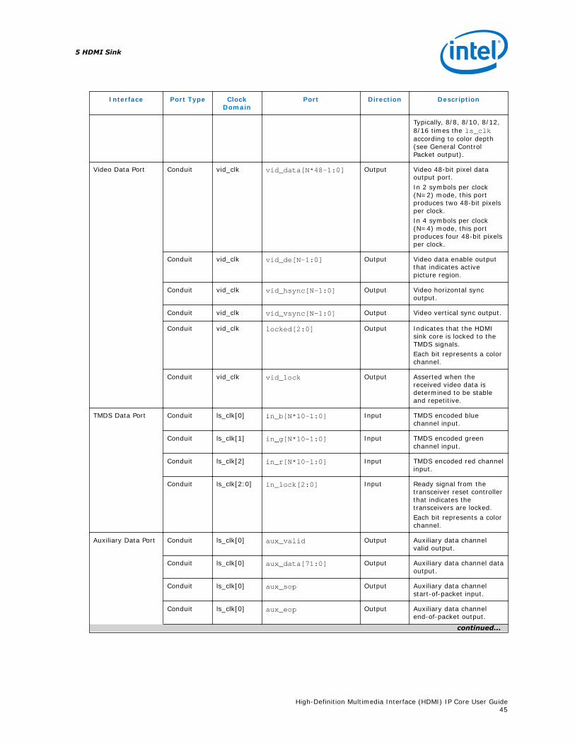
Interface Port Type ClockDomain
Port Direction Description
Typically, 8/8, 8/10, 8/12,8/16 times the ls_clkaccording to color depth(see General ControlPacket output).
Video Data Port Conduit vid_clk vid_data[N*48-1:0] Output Video 48-bit pixel dataoutput port.In 2 symbols per clock(N=2) mode, this portproduces two 48-bit pixelsper clock.In 4 symbols per clock(N=4) mode, this portproduces four 48-bit pixelsper clock.
Conduit vid_clk vid_de[N-1:0] Output Video data enable outputthat indicates activepicture region.
Conduit vid_clk vid_hsync[N-1:0] Output Video horizontal syncoutput.
Conduit vid_clk vid_vsync[N-1:0] Output Video vertical sync output.
Conduit vid_clk locked[2:0] Output Indicates that the HDMIsink core is locked to theTMDS signals.Each bit represents a colorchannel.
Conduit vid_clk vid_lock Output Asserted when thereceived video data isdetermined to be stableand repetitive.
TMDS Data Port Conduit ls_clk[0] in_b[N*10-1:0] Input TMDS encoded bluechannel input.
Conduit ls_clk[1] in_g[N*10-1:0] Input TMDS encoded greenchannel input.
Conduit ls_clk[2] in_r[N*10-1:0] Input TMDS encoded red channelinput.
Conduit ls_clk[2:0] in_lock[2:0] Input Ready signal from thetransceiver reset controllerthat indicates thetransceivers are locked.Each bit represents a colorchannel.
Auxiliary Data Port Conduit ls_clk[0] aux_valid Output Auxiliary data channelvalid output.
Conduit ls_clk[0] aux_data[71:0] Output Auxiliary data channel dataoutput.
Conduit ls_clk[0] aux_sop Output Auxiliary data channelstart-of-packet input.
Conduit ls_clk[0] aux_eop Output Auxiliary data channelend-of-packet output.
continued...
5 HDMI Sink
High-Definition Multimedia Interface (HDMI) IP Core User Guide45

Interface Port Type ClockDomain
Port Direction Description
Conduit ls_clk[0] aux_error Output Asserted when there isauxiliary data channel CRCerror.
Decoder ControlPort
Conduit ls_clk[0] TMDS_Bit_clock_Ratio Output • 0 = (TMDS bit period) /(TMDS clock period)ratio is 1/10
• 1 = (TMDS bit period) /(TMDS clock period)ratio is 1/40
Conduit ls_clk[0] ctrl[N*6-1:0] Output DVI Control side-bandsignals that show the datathat overwrite the controland synchronizationcharacter in the green andred channels.
Conduit ls_clk[0] mode Output Encoding mode• 0 = DVI• 1 = HDMI
Audio Port Conduit ls_clk[0] audio_CTS[19:0] Output Audio CTS value output.
Conduit ls_clk[0] audio_N[19:0] Output Audio N value output.
Conduit ls_clk[0] audio_data[255:0] Output Audio data output.
Conduit ls_clk[0] audio_de[7:0] Output Audio data valid output.
Conduit audio_clk audio_metadata[164:0]
Output Additional informationrelated to 3D audio andmulti-stream audio.
Conduit audio_clk audio_format[4:0] Output Indicates the audio formatdetected.
Conduit ls_clk[0] audio_info_ai[47:0] Output Audio InfoFrame inputbundle.
Auxiliary MemoryInterface
Conduit ls_clk[0] aux_pkt_addr[6:0] Output Auxiliary packet memorybuffer address output.
Conduit ls_clk[0] aux_pkt_data[71:0] Output Auxiliary packet memorybuffer data output.
Conduit ls_clk[0] aux_pkt_wr Output Auxiliary packet memorybuffer write strobe output.
Auxiliary ControlPort
Conduit ls_clk[0] gcp[5:0] Output General Control Packetoutput.
Conduit ls_clk[0] info_avi[111:0] Output Auxiliary VideoInformation InfoFrameoutput.
Conduit ls_clk[0] info_vsi[60:0] Output Vendor SpecificInformation InfoFrameoutput.
SCDC Control Port Conduit scdc_i2c_clk
in_5v_power Input Detects the presence of 5Vinput voltage.
Conduit scdc_i2c_clk
in_hpd Input Detects the Hot PlugDetect (HPD) status.
Misc. Conduit – version[31:0] Output Version of the HDMI core.
5 HDMI Sink
High-Definition Multimedia Interface (HDMI) IP Core User Guide46

5.2.1 Avalon-MM SCDC Management Interface
Table 25. Avalon-MM Status and Control Data Channel (SCDC) Management InterfaceSignalsThe table lists the Avalon Memory-Mapped (Avalon-MM) Status and Control Data Channel (SCDC) Managementinterface signals.
Signal Direction Description
scdc_i2c_clk Input Avalon-MM clock input.
scdc_i2c_addr[7:0] Input 8-bit Avalon-MM address.
scdc_i2c_r Input Read signal.
scdc_i2c_rdata[7:0] Output Output data.
scdc_i2c_w Input Write signal.
scdc_i2c_wdata[7:0] Input Input data.
For more information about SCDC, refer to the HDMI 2.0 Specification Section 10.4(Status and Control Data Channel).
5.2.2 Status and Control Data Channel Interface
For applications using the HDMI 2.0 feature, the HDMI IP core provides a memoryslave port to the SCDC registers.
This memory slave port connects to an I2C slave component. TheTMDS_Bit_clock_Ratio output from the SCDC interface indicates when the corerequires the 1/40 TMDS bit period to TMDS clock period. This bit is also stored in itscorresponding field in the SCDC registers.
The HDMI 2.0 specification requires the core to respond to the presence of the 5Vinput from the connector and also the state of the HPD signal. The 5V input and HPDsignal are used in the register mechanism updates. The signals are synchronous to thescdc_i2c_clk clock domain. You must create a 100-ms delay on the HPD signalexternally to the core.
For more information about the Status and Control Data Channel, you may refer toHDMI 2.0 Specification Chapter 10.4.You can obtain the address map for the registersin the HDMI 2.0 specification.
5.3 Sink Clock Tree
The sink core uses different clocks.
The logic clocks the transceiver data into the core using the three CDR clocks:(rx_clk[2:0]).
The TMDS and TERC4 decoding is done at the link-speed clock (ls_clk). The sink thenresamples the pixel data and presents the data at the output of the core at the videopixel clock (vid_clk).
The pixel data clock depends on the video format used (within HDMI specification).
For HDMI sink, you need to instantiate 3 receiver channels to receive data.
5 HDMI Sink
High-Definition Multimedia Interface (HDMI) IP Core User Guide47

Figure 34. Sink Clock TreeThe figure shows how the different clocks can be selected for the sink core.
ResamplerFIFO
Sync
TMDS(TERC4)Decoder
Sync
Sync
HSSI[0]
HSSI[1]
HSSI[2]
HDMI Sink Core
Channel [0]
reconfig
Channel [1]
Channel [2]
WRCLK RDCLK
WRCLK RDCLK
WRCLK RDCLK
WRCLK RDCLK
rx_clk[0] vid_clk
Pixel Data
AUX Data
Transceiver
GPLLCLK0CLK1CLK2
ls_clkvid_clk
ls_clk
TMDS Clock
CDR Reference Clock
rx_clk[1]
rx_clk[2]
Related Links
HDMI Hardware Demonstration on page 52For more information about the transmitter and receiver channels.
5 HDMI Sink
High-Definition Multimedia Interface (HDMI) IP Core User Guide48

6 HDMI ParametersUse the settings in the HDMI parameter editor to configure your design.
6.1 HDMI Source Parameters
Table 26. HDMI Source Parameters
Parameter Value Description
Device family Stratix VArria VArria 10
Targeted device family; matches the project devicefamily.
Direction Transmitter = SourceReceiver = Sink
Select HDMI source.
Symbols per clock 1, 2, or 4 symbols per clock Determines how many TMDS symbols and pixelsare processed per clock.• Stratix V supports 1 or 2 symbols per clock• Arria V supports 1, 2, or 4 symbols per clock• Arria 10 supports only 2 symbols per clock
Support auxiliary 0 = No AUX1 = AUX
Determines if auxiliary channel encoding isincluded.
Support deep color 0 = No deep color1 = Deep color
Determines if the core can encode deep colorformats.To enable this parameter, you must also enable theSupport auxiliary parameter.
Support audio 0 = No audio1 = Audio
Determines if the core can encode audio data.To enable this parameter, you must also enable theSupport auxiliary parameter.
6.2 HDMI Sink Parameters
Table 27. HDMI Sink Parameters
Parameter Value Description
Device family Stratix VArria VArria 10
Targeted device family; matches the project devicefamily.
Direction Transmitter = SourceReceiver = Sink
Select HDMI sink.
Symbols per clock 1, 2, or 4 symbols per clock Determines how many TMDS symbols and pixelsare processed per clock.
continued...
6 HDMI Parameters
Intel Corporation. All rights reserved. Intel, the Intel logo, Altera, Arria, Cyclone, Enpirion, MAX, Nios, Quartusand Stratix words and logos are trademarks of Intel Corporation or its subsidiaries in the U.S. and/or othercountries. Intel warrants performance of its FPGA and semiconductor products to current specifications inaccordance with Intel's standard warranty, but reserves the right to make changes to any products and servicesat any time without notice. Intel assumes no responsibility or liability arising out of the application or use of anyinformation, product, or service described herein except as expressly agreed to in writing by Intel. Intelcustomers are advised to obtain the latest version of device specifications before relying on any publishedinformation and before placing orders for products or services.*Other names and brands may be claimed as the property of others.
ISO9001:2008Registered

Parameter Value Description
• Stratix V supports 1 or 2 symbols per clock• Arria V supports 1, 2, or 4 symbols per clock• Arria 10 supports only 2 symbols per clock
Support auxiliary 0 = No AUX1 = AUX
Determines if auxiliary channel encoding isincluded.
Support deep color 0 = No deep color1 = Deep color
Determines if the core can encode deep colorformats.To enable this parameter, you must also enable theSupport auxiliary parameter.
Support audio 0 = No audio1 = Audio
Determines if the core can encode audio data.To enable this parameter, you must also enable theSupport auxiliary parameter.
Manufacturer OUI — The Manufacturer Organizationally Unique Identifier(OUI) assigned to the manufactured device to bewritten into the SCDC registers of address 0xD0,0xD1, and 0xD2.Key in 3 byte hexadecimal data.
Device ID String — The Device Identification (ID) string to be writteninto the SCDC registers from addresses 0xD3 to0xDa.Use this parameter to identify the sink device. Youcan key in up to eight ASCII characters. If you useless than eight characters, the unused bytes are setto 0x00.
Hardware Revision — Indicates the major and minor revisions of thehardware. Key in one byte of integer data.• Upper byte represents major revision.• Lower byte represents minor revision.The hardware major revision increments on amajor silicon or board revision. The hardware minorrevision increments on a minor silicon revision orminor board revision and resets to 0 when themajor revision increments.
6.3 HDMI Design Example Parameters
Table 28. HDMI Design Example ParametersThese options are available for Arria 10 devices only.
Parameter Value Description
Available Design Example
Select Design None, Arria 10 HDMIRX-TX Retransmit
Select the design example to be generated.• None: No design example is available for the current parameter
selection• Arria 10 HDMI RX-TX Retransmit: The generated design example
which has preconfigured parameter settings—does not follow usersettings.
Design Example Files
Simulation On, Off Turn on this option to generate the necessary files for the simulationtestbench.
Synthesis On, Off Turn on this option to generate the necessary files for Quartus Primecompilation and hardware demonstration.
6 HDMI Parameters
High-Definition Multimedia Interface (HDMI) IP Core User Guide50

Generated HDL Format
Generate File Format Verilog, VHDL Select your preferred HDL format for the generated design examplefileset.Note: This option only determines the format for the generated top
level IP files. All other files (e.g. example testbenches and toplevel files for hardware demonstration) are in Verilog HDL format.
Target Development Kit
Select Board No Development Kit,Arria 10 GX FPGADevelopment Kit,
Custom DevelopmentKit
Select the board for the targeted design example.• No Development Kit: This option excludes all hardware aspects for
the design example. The IP core sets all pin assignments to virtualpins.
• Arria 10 GX FPGA Development Kit: This option automatically selectsthe project's target device to match the device on this developmentkit. You may change the target device using the Change TargetDevice parameter if your board revision has a different devicevariant. The IP core sets all pin assignments according to thedevelopment kit.
• Custom Development Kit: This option allows the design example tobe tested on a third party development kit with an Intel FPGA. Youmay need to set the pin assignments on your own.
Target Device
Change Target Device On, Off Turn on this option and select the preferred device variant for thedevelopment kit.
6 HDMI Parameters
High-Definition Multimedia Interface (HDMI) IP Core User Guide51

7 HDMI Hardware DemonstrationThe High-Definition Multimedia Interface (HDMI) hardware demonstration helps youevaluate the functionality of the HDMI IP core and provides a starting point for you tocreate your own design.
The demonstration runs on the following device kits:
• Arria V GX starter kit
• Stratix V GX development kit
Related Links
AN 745: Design Guidelines for DisplayPort and HDMI Interfaces
7.1 Hardware Demonstration Components
The demonstration designs instantiate the Video and Image Processing (VIP) Suite IPcores or FIFO buffers to perform a direct HDMI video stream passthrough between theHDMI sink and source.
7 HDMI Hardware Demonstration
Intel Corporation. All rights reserved. Intel, the Intel logo, Altera, Arria, Cyclone, Enpirion, MAX, Nios, Quartusand Stratix words and logos are trademarks of Intel Corporation or its subsidiaries in the U.S. and/or othercountries. Intel warrants performance of its FPGA and semiconductor products to current specifications inaccordance with Intel's standard warranty, but reserves the right to make changes to any products and servicesat any time without notice. Intel assumes no responsibility or liability arising out of the application or use of anyinformation, product, or service described herein except as expressly agreed to in writing by Intel. Intelcustomers are advised to obtain the latest version of device specifications before relying on any publishedinformation and before placing orders for products or services.*Other names and brands may be claimed as the property of others.
ISO9001:2008Registered

The hardware demonstration design comprises the following components:
• HDMI sink
— Transceiver Native PHY (RX)
— Transceiver PHY Reset Controller (RX)
— Altera PLL
— Altera PLL Reconfiguration
— Multirate Reconfiguration Controller (RX)
— Oversampler (RX)
— DCFIFO
• Sink Display Data Channel (DDC) and Status and Control Data Channel (SCDC)
• Transceiver Reconfiguration Controller
• VIP bypass and audio, auxiliary and infoframe buffers
• Qsys system
— VIP passthrough for HDMI video stream
— Source SCDC controller
— HDMI source reconfiguration controller
• HDMI source
— Transceiver Native PHY (TX)
— Transceiver fPLL
— Transceiver PHY Reset Controller (TX)
— Altera PLL
— Altera PLL Reconfiguration
— Oversampler (TX)
— DCFIFO
— Clock Enable Generator
7 HDMI Hardware Demonstration
High-Definition Multimedia Interface (HDMI) IP Core User Guide53

Figure 35. HDMI Hardware Demonstration Block DiagramThe figure below shows a high level architecture of the design.
RX TDMS Clock
TX Transceiver Reference Clock
TX Transceiver Clock Out
TX Link Speed Clock
TX Video Clock
I C Clock
Memory Clock
RX Transceiver Reference Clock
RX Transceiver Recovered Clock
RX Link Speed Clock
RX Video Clock
Management Clock
VIP Main Clock 2
Sink DDC and SCDC
Altera PLLIP Core
Altera PLLReconfiguration
IP Core
Transceiver PHYReset Controller
(RX) IP Core
Transceiver Native PHY(RX) IP Core
Oversampler(RX)
HDMI Source
Avalon-MM MasterTranslator
(13)
Qsys System (HDMI Source, SCDC Control, and VIP Passthrough)
Avalon-MM SlaveTranslator
Avalon-MM SlaveTranslator
Nios II CPU
Video FrameBuffer IP Core
Clocked VideoInput IP Core
Clocked VideoOutput IP Core
External MemoryController IP Core
Transceiver ReconfigurationController IP Core
External Memory(DDR3)
VIP Bypass and Audio/Aux/IF Buffers
Source SCDC
Altera HDMIIP Core (TX)
(14)
(5) (6) (7)
Clock EnableGenerator
Transceiver NativePHY (TX) IP Core
(2)DCFIFOIP Core (2)
Altera HDMIIP Core (RX)
RateDetect
Multi-RateReconfigurationController (RX)(12)
(1)
(3)
HDMI Sink
I2C Slave(SCDC) (15)
I2C Slave(EDID)
RAM 1-PortIP Core
I2C Master(SCDC)
DCFIFOIP Core
DCFIFOIP Core
DCFIFOIP Core (8)
Oversampler(TX) (8)
(9)
Transceiver PHYReset Controller
(TX) IP Core
Altera PLLReconfiguration
IP Core
Altera PLLIP Core
(10)
(14)
(5)(4)
(11)
DataAvalon-ST Video
Avalon-MMControl/Status
Arrow Legend
Clock Legend
The following details of the example design architecture correspond to the numbers inthe block diagram.
1. The sink TMDS data has three channels: data channel 0 (blue), data channel 1(green), and data channel 2 (red).
2. The Oversampler (RX) and dual-clock FIFO (DCFIFO) instances are duplicated foreach TMDS data channel (0,1,2).
3. The video data input width for each color channel of the HDMI RX core isequivalent to RX transceiver PCS-PLD parallel data width per channel.
4. Each color channel is fixed at 16 bits per color. The video data output width of theHDMI RX core is equivalent to the value of symbols per clock*16*3.
5. The video data input width of the Clocked Video Input (CVI) and Clocked VideoOutput (CVO) IP cores are equivalent to the value ofNUMBER_OF_PIXELS_IN_PARALLEL * BITS_PER_PIXEL_PER_COLOR_PLANE *NUMBER_OF_COLOR_PLANES. To interface with the HDMI core, the values ofNUMBER_OF_PIXELS_IN_PARALLEL, BITS_PER_PIXEL_PER_COLOR_PLANE, andNUMBER_OF_COLOR_PLANES must match the symbols per clock, 16 and 3respectively.
6. The video data input width of the HDMI TX core is equivalent to the value ofsymbols per clock*16*3. You can use the user switch to select the video data fromthe CVO IP core (VIP passthrough) or DCFIFO (VIP bypass).
7. The video data output width for each color channel of the HDMI TX core isequivalent to TX transceiver PCS-PLD parallel data width per channel.
8. The DCFIFO and the Oversampler (TX) instances are duplicated for each TMDSdata channel (0,1,2) and clock channel.
9. The Oversampler (TX) uses the clock enable signal to read data from the DCFIFO.
10. The source TMDS data has four channels: data channel 0 (blue), data channel 1(green), data channel 2 (red), and clock channel.
7 HDMI Hardware Demonstration
High-Definition Multimedia Interface (HDMI) IP Core User Guide54

11. The RX Multi-rate Reconfiguration Controller requires the status ofTMDS_Bit_clock_ Ratio port to perform appropriate RX reconfigurationbetween the TMDS character rates below 340 Mcsc (HDMI 1.4b) and above 340Mcsc (HDMI 2.0). The status of the port is also required by the Nios II processorand the HDMI TX core to perform appropriate TX reconfiguration and scrambling.
12. The reset control and lock status signals from HDMI PLL, RX Transceiver ResetController and HDMI RX core.
13. The reset and oversampling control signals for HDMI PLL, TX Transceiver ResetController, and HDMI TX core. The lock status and rate detection measure validsignals from the HDMI sink initiate the TX reconfiguration process.
14. The I2C SCL and SDA lines with tristate buffer for bidirectional configuration. Usethe ALTIOBUF IP core for Arria V and Stratix V devices.
15. The SCDC is mainly designed for the source to update theTMDS_Bit_Clock_Ratio and Scrambler_Enable bits of the sink TMDSConfiguration register. The HDMI RX core does not support SCDC read requestfeature for this release.
7.1.1 Transceiver Native PHY (RX)
• Transceiver Native PHY in Arria V devices
— To operate the TMDS bit rate up to 3,400 Mbps, configure the TransceiverNative PHY at 20 bits at PCS – PLD interface with the HDMI RX core at 2symbols per clock. When the PCS – PLD interface width is 20 bits, theminimum link rate is 611 Mbps.
— To operate the TMDS bit rate up to 6,000 Mbps, configure the TransceiverNative PHY at 40 bits with the HDMI RX core at 4 symbols per clock. When thePCS – PLD interface width is 40 bits, the minimum link rate is 1,000 Mbps.
— Oversampling is required for TMDS bit rate which is below the minimum linkrate.
• Transceiver Native PHY in Stratix V devices
— To operate the TMDS bit rate up to 6,000 Mbps, configure the TransceiverNative PHY at 20 bits at PCS – PLD interface with the HDMI RX core at 2symbols per clock. When the PCS – PLD interface width is 20 bits, theminimum link rate is 611 Mbps.
Table 29. Arria V and Stratix V Transceiver Native PHY (RX) Configuration Settings(6,000 Mbps)This table shows an example of Arria V and Stratix V Transceiver Native PHY (RX) configuration settings forTMDS bit rate of 6,000 Mbps.
Parameters Settings
Datapath Options
Enable TX datapath Off
Enable RX datapath On
Enable Standard PCS On
Initial PCS datapath selection Standard
Number of data channels 3
Enable simplified data interface On
7 HDMI Hardware Demonstration
High-Definition Multimedia Interface (HDMI) IP Core User Guide55

RX PMA
Data rate 6,000 Mbps
Enable CDR dynamic reconfiguration On
Number of CDR reference clocks 2 2
Selected CDR reference clock 0 2
Selected CDR reference clock frequency 600 MHz
PPM detector threshold 1,000 PPM
Enable rx_pma_clkout port On
Enable rx_is_lockedtodata port On
Enable rx_is_lockedtoref port On
Enable rx_set_locktodata and rx_set_locktoref ports On
Standard PCS
Standard PCS protocol Basic
Standard PCS/PMA interface width• 10 (for 1 symbol per clock)• 20 (for 2 and 4 symbols per clock)
Enable RX byte deserializer• Off (for 1 and 2 symbols per clock)• On (for 4 symbols per clock)
2 The Bitec HDMI 2.0 HSMC daughter card routes the TMDS clock pin to the transceiver serialdata pin. To use the TMDS clock to drive the HDMI PLL, the TMDS clock must also drive thetransceiver dedicated reference clock pin. The number of CDR reference clocks is 2 withreference clock 1 (unused) driven by the TMDS clock and reference clock 0 driven by the HDMIPLL output clock. The selected CDR reference clock will be fixed at 0.
7 HDMI Hardware Demonstration
High-Definition Multimedia Interface (HDMI) IP Core User Guide56

Table 30. Arria V and Stratix V Transceiver Native PHY (RX) Common Interface PortsThis table describes the Arria V and Stratix V Transceiver Native PHY (RX) common interface ports.
Signals Direction Description
Clocks
rx_cdr_refclk[1:0] Input Input reference clock for the RX CDR circuitry.• To support arbitrary wide data rate range from 250 Mbps
to 6,000 Mbps, you need a generic core PLL to obtain ahigher clock frequency from the TMDS clock. You need ahigher clock frequency to create oversampled stream fordata rates below the minimum transceiver data rate—forexample, 611 Mbps or 1,000 Mbps).
• If the TMDS clock pin is routed to the transceiverdedicated reference clock pin, you only need to createone transceiver reference clock input. You can use theTMDS clock as reference clock for a generic core PLL todrive the transceiver.
• If you use Bitec HDMI 2.0 HSMC daughter card, theTMDS clock pin is routed to the transceiver serial datapin. In this case, to use the TMDS clock as a referenceclock for a generic core PLL, the clock must also drivethe transceiver dedicated reference clock. Connect bit 0to the generic core PLL output and bit 1 to the TMDSclock and set the selected CDR reference clock at 0.
rx_std_clkout[2:0] Output RX parallel clock output.• The CDR circuitry recovers the RX parallel clock from the
RX data stream when the CDR is configured at lock-to-data mode.
• The RX parallel clock is a mirror of the CDR referenceclock when the CDR is configured at lock-to-referencemode.
rx_std_coreclkin[2:0] Input RX parallel clock that drives the read side of the RX phasecompensation FIFO.Connect to rx_std_clkout ports.
rx_pma_clkout[2:0] Output RX parallel clock (recovered clock) output from PMA.Leave unconnected.
Resets
rx_analogreset[2:0] Input Active-high, edge-sensitive, asynchronous reset signal.When asserted, resets the RX CDR circuit, deserializer.Connect to Transceiver PHY Reset Controller IP core.
rx_digitalreset[2:0] Input Active-high, edge-sensitive, asynchronous reset signal.When asserted, resets the digital component of the RX datapath.Connect to the Transceiver PHY Reset Controller IP core.
PMA Ports
rx_set_locktoref[2:0] Input When asserted, programs the RX CDR to lock to referencemode manually. The lock to reference mode enables you tocontrol the reset sequence using rx_set_locktoref andrx_set_locktodata.The Multirate Reconfiguration Controller (RX) sets this portto 1 if oversampling mode is required. Otherwise, this portis set to 0.
continued...
7 HDMI Hardware Demonstration
High-Definition Multimedia Interface (HDMI) IP Core User Guide57

PMA Ports
Refer "Transceiver Reset Sequence" in Transceiver ResetControl in Arria V/Stratix V Devices for more informationabout manual control of the reset sequence.
rx_set_locktodata[2:0] Input Always driven to 0. When rx_set_locktoref is driven to1, the CDR is configured to lock-to-reference mode.Otherwise, the CDR is configured to lock-to-data mode.
rx_is_lockedtoref[2:0] Output When asserted, the CDR is locked to the incoming referenceclock. Connect this port to rx_is_lockedtodata port ofthe Transceiver PHY Reset Controller IP core whenrx_set_locktoref is 1.
rx_is_lockedtodata[2:0] Output When asserted, the CDR is locked to the incoming data.Connect this port to rx_is_lockedtodata port ofTransceiver PHY Reset Controller IP core whenrx_set_locktoref is 0.
rx_serial_data[2:0] Input RX differential serial input data.
PCS Ports
unused_rx_parallel_data Output Leave unconnected.
rx_parallel_data[S*3*10-1:0]
Output PCS RX parallel data.Note: S=Symbols per clock.
Calibration Status Port
rx_cal_busy[2:0] Output When asserted, indicates that the initial RX calibration is inprogress. This port is also asserted if the reconfigurationcontroller is reset. Connect to the Transceiver PHY ResetController IP core.
Reconfiguration Ports
reconfig_to_xcvr[209:0] Input Reconfiguration signals from the Transceiver ReconfigurationController.
reconfig_from_xcvr[137:0] Output Reconfiguration signals to the Transceiver ReconfigurationController.
7.1.2 Altera PLL IP Cores
Use the Altera PLL IP core as the HDMI PLL to generate reference clock for RX or TXtransceiver, link speed, and video clocks for the HDMI RX or TX IP core.
The HDMI PLL is referenced by the arbitrary TMDS clock. For HDMI source, you canreference the HDMI PLL by a separate clock source in the VIP passthrough design,which contains frame buffer. The HDMI PLL for TX has the same desired outputfrequencies as RX across symbols per clock and color depth.
• For TMDS bit rates ranging from 3,400 Mbps to 6,000 Mbps (HDMI 2.0), the TMDSclock rate is 1/40 of the TMDS bit rate. The HDMI PLL generates reference clockfor RX/TX transceiver at 4 times the TMDS clock.
• For TMDS bit rates below 3,400 Mbps (HDMI 1.4b), the TMDS clock rate is 1/10 ofthe TMDS bit rate. The HDMI PLL generates reference clock for RX/TX transceiverat identical rate as the TMDS clock.
7 HDMI Hardware Demonstration
High-Definition Multimedia Interface (HDMI) IP Core User Guide58

If the TMDS link operates at TMDS bit rates below the minimum RX/TX transceiver linkrate, your design requires oversampling and a factor of 5 is chosen. The minimum linkrate of the RX/TX transceiver vary across device families and symbols per clock. TheHDMI PLL generates reference clock for RX/TX transceiver at 5 times the TMDS clock.
Note: Place the Altera PLL in the transmit path (pll_hdmi_tx) in the physical location nextto the transceiver PLL.
Table 31. HDMI PLL Desired Output Frequencies for 8-bpc VideoThis table shows an example of HDMI PLL desired output frequencies across various TMDS clock rates andsymbols per clock for all supported device families using 8-bpc video.
DeviceFamily
SymbolsPer
Clock
MinimumLink Rate(Mbps)
TMDS BitRate
(Mbps)
Oversampling (5x)
Required
TMDSClock Rate
(MHz)
RX/TXTransceiver Refclk
(MHz)
RX/TXLink
SpeedClock(MHz)
RX/TXVideoClock(MHz)
Arria V
2 611
270 Yes 27 135 13.5 13.5
742.5 No 74.25 74.25 37.125 37.125
1,485 No 148.5 148.5 74.25 74.25
2,970 No 297 297 148.5 148.5
4 1,000
270 Yes 27 135 6.75 6.75
742.5 Yes 74.25 371.25 18.5625 18.5625
1,485 No 148.5 148.5 37.125 37.125
5,940 No 148.5 594 148.5 148.5
Stratix V 2 611
540 Yes 54 270 27 27
1,620 No 162 162 81 81
5,934 No 296.7 593.4 296.7 296.7
The color depths greater than 8 bpc or 24 bpp are defined to be deep color. For a colordepth of 8 bpc, the core carries the pixels at a rate of one pixel per TMDS clock. Atdeeper color depths, the TMDS clock runs faster than the source pixel clock to providethe extra bandwidth for the additional bits.
The TMDS clock rate is increased by the ratio of the pixel size to 8 bits:
• 8 bits mode—TMDS clock = 1.0 × pixel or video clock (1:1)
• 10 bits mode—TMDS clock = 1.25 × pixel or video clock (5:4)
• 12 bits mode—TMDS clock = 1.5 × pixel or video clock (3:2)
• 16 bits mode—TMDS clock = 2 × pixel or video clock (2:1)
7 HDMI Hardware Demonstration
High-Definition Multimedia Interface (HDMI) IP Core User Guide59

Table 32. HDMI PLL Desired Output Frequencies for Deep Color VideoThis table shows an example of HDMI PLL desired output frequencies across symbols per clock and colordepths.
Symbols PerClock
Oversampling
(5x)Require
d
Bits percolor
TMDS BitRate (Mbps)
TMDS ClockRate (MHz)
RX/TXTransceiver
Refclk (MHz)
RX/TX LinkSpeed Clock
(MHz)
RX/TX VideoClock (MHz)
2 Yes
8 270 27 135 13.5 13.5
10 3 337.5 33.75 168.75 16.875 13.5
12 3 405 40.5 202.5 20.25 13.5
16 3 540 54 270 27 13.5
4 No
8 1,485 148.5 148.5 37.125 37.125
10 3 1,856.25 185.625 185.625 46.40625 37.125
12 3 2,227.5 222.75 222.75 55.6875 37.125
16 3 2,970 297 297 74.25 37.125
The default frequency setting of the HDMI PLL is fixed at possible maximum value foreach clock for appropriate timing analysis.
Note: This default combination is not valid for any HDMI resolution. The core will reconfigureto the appropriate settings upon power up.
7.1.3 Altera PLL Reconfig IP Core
The Altera PLL Reconfig IP core facilitates dynamic real-time reconfiguration of PLLs inIntel FPGAs.
Use the IP core to update the output clock frequency, PLL bandwidth in real-time,without reconfiguring the entire FPGA.
You can run this IP core at 100 MHz in Arria 10 and Stratix V devices. In Arria Vdevices, you need to run at 75 MHz for timing closure. To simplify clocking in Arria Vdevices, the entire management clock domain is capped at 75 MHz.
7.1.4 Multirate Reconfig Controller (RX)
The Multirate Reconfig Controller implements rate detection circuitry with the HDMIPLL to drive the RX transceiver to operate at any arbitrary link rates ranging from 250Mbps to 6,000 Mbps. Link rate of 6,000 Mbps is not the absolute maximum but theintention is to support HDMI 2.0 link rate.
The Multirate Reconfig Controller performs rate detection on the HDMI PLL arbitraryreference clock, which is also the TMDS clock, to determine the clock frequency band.Based on the detected clock frequency band, the circuitry dynamically reconfiguresthe HDMI PLL and transceiver settings to accommodate for the link rate change.
3 For this release, deep color video is only demonstrated in VIP bypass mode. It is not availablein VIP passthrough mode.
7 HDMI Hardware Demonstration
High-Definition Multimedia Interface (HDMI) IP Core User Guide60

Figure 36. Multirate Reconfiguration Sequence FlowThis figure illustrates the multirate reconfiguration sequence flow of the controllerwhen it receives input data stream and reference clock frequency, or when thetranceiver is unlocked.
Reset the RX HDMI PLL and RX transceiver.
Enable the rate detection circuit to measure incoming TMDS clock.
Accept acknowledgement with clock frequency band and desired RX HDMI PLL and RX transceiver settings.
Determine if RX HDMI PLL and/or RX transceiver reconfiguration is required based on the previous and current detected clock frequency band and color depth. Different color depths may fall within the same clock frequency band.
Request RX HDMI PLL and/or RX transceiver reconfiguration if the previous and current clock frequency band or color depth differs.
The controller reconfigures the RX HDMI PLL and/or RX transceiver (followed by recalibration on Arria 10 device).
When all reconfiguration processes complete or the previous and current clock frequency band and color depth do not differ, reset the RX HDMI PLL and RX transceiver.
Enable rate the detection circuit periodically to monitor the reference clock frequency. If the clock frequency band changes or the RX HDMI PLL or RX transceiver or HDMI core lose lock, repeat the process.
Reconfiguration Is Required Reconfiguration Is Not Required
7.1.5 Oversampler (RX)
The Oversampler (RX) extracts data from the oversampled incoming data streamwhen the detected clock frequency band is below the transceiver minimum link rate.
The oversampling factor is fixed at 5 and you can program the data width to supportdifferent number of symbols. The supported data width is 20 bit for 2 symbols perclock and 40 bits for 4 symbols per clock. The extracted bit will be accompanied bydata valid pulse which asserts every 5 clock cycles.
7 HDMI Hardware Demonstration
High-Definition Multimedia Interface (HDMI) IP Core User Guide61

7.1.6 DCFIFO
The DCFIFO transfers data from the RX transceiver recovered clock domain to the RXlink speed clock domain. The DCFIFO transfers data from the TX link speed clockdomain to the TX transceiver parallel clock out domain.
• Sink
— When the Multirate Reconfig Controller (RX) detects an incoming input streamthat is below the transceiver minimum link rate, the DCFIFO accepts the datafrom the Oversampler with data valid pulse as write request asserted every 5clock cycles.
— Otherwise, it accepts data directly from the transceiver with write requestasserted at all times.
• Source
— When Nios II processor determines the outgoing data stream is below the TXtransceiver minimum link rate, the TX transceiver accepts the data from theOversampler (TX).
— Otherwise, the TX transceiver reads data directly from the DCFIFO with readrequest asserted at all times.
7.1.7 Sink Display Data Channel (DDC) & Status and Control Data Channel(SCDC)
The HDMI source uses the DDC to determine the capabilities and characteristics of thesink by reading the Enhanced Extended Display Identification Data (E-EDID) datastructure.
The E-EDID memory is stored using the RAM 1-Port IP core. A standard two-wire(clock and data) serial data bus protocol (I2C slave-only controller) is used to transferCEA-861-D compliant E-EDID data structure.
The 8-bit I2C slave addresses for the E-EDID are 0xA0/0xA1. The LSB indicates theaccess type: 1 for read and 0 for write. When an HPD event occurs, the I2C slaveresponds to E-EDID data by reading from the RAM.
The I2C slave-only controller is also used to support SCDC for HDMI 2.0 operation. The8-bit I2C slave addresses for the SCDC are 0xA8/0xA9. When an HPD event occurs,the I2C slave performs write/read transaction to/from SCDC interface of HDMI RXcore. This I2C slave-only controller for SCDC is not required if HDMI 2.0 is notintended.
7.1.8 Transceiver Reconfiguration Controller
You can use the Transceiver Reconfiguration Controller IP core to change the devicetransceiver settings at any time.
You can selectively reconfigure any portion of the transceiver. The reconfiguration ofeach portion requires a read-modify-write operation (read first, then write). The read-modify-write operation modifies only the appropriate bits in a register and does notaffect the other bits.
7 HDMI Hardware Demonstration
High-Definition Multimedia Interface (HDMI) IP Core User Guide62

The Transceiver Reconfiguration Controller is only available and required in Arria V andStratix V devices. Because the RX and TX transceivers share a single controller, thecontroller requires Qsys interconnects, such as Avalon-MM Master Translator andAvalon-MM Slave Translator, in the Qsys system.
• The Avalon-MM Master Translator provides an interface between this controller andthe RX Multirate Reconfig Controller.
• The Avalon-MM Slave Translator arbitrates the RX and TX reconfiguration event forthis controller.
In Arria 10 devices, the Transceiver Native PHY has a direct access the Avalon-MMreconfiguration interface.
• The RX Multirate Reconfig Controller directly drives the RX transceiverreconfiguration interface.
• The Avalon-MM Slave Translator converts the Nios II reconfiguration command anddirectly drives the TX transceiver reconfiguration interface.
7.1.9 VIP Bypass and Audio, Auxiliary and InfoFrame Buffers
The video data output and synchronization signals from HDMI RX core is loopedthrough a DCFIFO across RX and TX video clock domains. The General Control Packet(GCP), InfoFrames (AVI, VSI, and AI), auxiliary data and audio data are loopedthrough DCFIFOs across RX and TX link speed clock domains.
The auxiliary data port of the HDMI TX core controls the auxiliary data that flowthrough DCFIFO through backpressure. The backpressure ensures there is noincomplete auxiliary packet on the auxiliary data port. This block also performsexternal filtering on the audio data and audio clock regeneration packet from theauxiliary data stream before sending to the HDMI TX core auxiliary data port.
7.1.10 Transceiver Native PHY (TX)
The Arria V and Stratix V Transceiver Native PHY (TX) configuration settings aretypically the same as RX.
Table 33. Arria V and Stratix V Transceiver Native PHY (TX) Configuration Settings(6,000 Mbps)This table shows an example of Arria V and Stratix V Transceiver Native PHY (TX) configuration settings forTMDS bit rate of 6,000 Mbps.
Parameters Settings
Datapath Options
Enable TX datapath On
Enable RX datapath Off
Enable Standard PCS On
Initial PCS datapath selection Standard
Number of data channels 4
Bonding mode xN
Enable simplified data interface On
7 HDMI Hardware Demonstration
High-Definition Multimedia Interface (HDMI) IP Core User Guide63

TX PMA
Data rate 6,000 Mbps
TX local clock division factor 1
Enable TX PLL dynamic reconfiguration On
Use external TX PLL Off
Number of TX PLLs 1
Main TX PLL logical index 0
Number of TX PLL reference clocks 1
PLL type CMU
Reference clock frequency 600 MHz
Selected reference clock source 0
Selected clock network xN
Standard PCS
Standard PCS protocol Basic
Standard PCS/PMA interface width• 10 (for 1 symbol per clock)• 20 (for 2 and 4 symbols per clock)
Enable TX byte serializer• Off (for 1 and 2 symbols per clock)• On (for 4 symbols per clock)
Table 34. Arria V and Stratix V Transceiver Native PHY (TX) Common Interface PortsThis table describes the Arria V and Stratix V Transceiver Native PHY (TX) common interface ports.
Signals Direction Description
Clocks
tx_pll_refclk Input The reference clock input to the TX PLL.
tx_std_clkout[3:0] Output TX parallel clock output.
tx_std_coreclkin[3:0] Input TX parallel clock that drives the write side of the TX phasecompensation FIFO.Connect to tx_std_clkout[0] ports.
Resets
tx_analogreset[3:0] Input When asserted, resets all the blocks in TX PMA.Connect to Transceiver PHY Reset Controller (TX) IP core.
tx_digitalreset[3:0] Input When asserted, resets all the blocks in TX PCS.Connect to the Transceiver PHY Reset Controller (TX) IPcore.
TX PLL
pll_powerdown Input When asserted, resets the TX PLL.Connect to the Transceiver PHY Reset Controller (TX) IPcore.
pll_locked Output When asserted, indicates that the TX PLL is locked.Connect to the Transceiver PHY Reset Controller (TX) IPcore.
7 HDMI Hardware Demonstration
High-Definition Multimedia Interface (HDMI) IP Core User Guide64

PCS Ports
unused_tx_parallel_data Input Leave unconnected.
tx_parallel_data[S*4*10-1:0]
Input PCS TX parallel data.Note: S=Symbols per clock.
PMA Port
tx_serial_data[3:0] Output TX differential serial output data.
Calibration Status Port
tx_cal_busy[3:0] Output When asserted, indicates that the initial TX calibration is inprogress. This port is also asserted if the reconfigurationcontroller is reset. Connect to the Transceiver PHY ResetController (TX) IP core.
Reconfiguration Ports
reconfig_to_xcvr[349:0] Input Reconfiguration signals from the Transceiver ReconfigurationController.
reconfig_from_xcvr[229:0] Output Reconfiguration signals to the Transceiver ReconfigurationController.
7.1.11 Transceiver PHY Reset Controller
The Transceiver PHY Reset Controller IP core ensures a reliable initialization of the RXand TX transceivers.
The reset controller has separate reset controls per channel to handle synchronizationof reset inputs, lagging of PLL locked status, and automatic or manual reset recoverymode.
7.1.12 Oversampler (TX)
The Oversampler (TX) transmits data by repeating each bit of the input word a givennumber of times and constructs the output words.
The oversampling factor is fixed at 5. The Oversampler (TX) assumes that the inputword is only valid every 5 clock cycles. This block enables when the outgoing datastream is determined to be below the TX transceiver minimum link rate by readingonce from the DCFIFO every 5 clock cycles.
7.1.13 Clock Enable Generator
The Clock Enable Generator is a logic that generates a clock enable pulse.
This clock enable pulse asserts every 5 clock cycles and serves as a read requestsignal to clock the data out from DCFIFO.
7.1.14 Qsys System
The Qsys system consists of the VIP passthrough for HDMI video stream, source SDCcontroller, and source reconfiguration controller blocks.
7 HDMI Hardware Demonstration
High-Definition Multimedia Interface (HDMI) IP Core User Guide65

7.1.14.1 VIP Passthrough for HDMI Video Stream
For certain example designs, you can loop the video data output and synchronizationsignals from HDMI RX core through the VIP data path.
The Clocked Video Input II (CVI II) IP core converts clocked video formats to Avalon-ST video by stripping incoming clocked video of horizontal and vertical blanking,leaving only active picture data.
• The IP core provides clock crossing capabilities to allow video formats running atdifferent frequencies to enter the system.
• The IP core also detects the format of the incoming clocked video and providesthis information in a set of registers.
• The Nios II processor uses this information to reconfigure the video frame moderegisters of the CVO IP core in the VIP passthrough design.
The Video Frame Buffer II IP core buffers video frames into external RAM.
• The IP core supports double and triple buffering with a range of options for framedropping and repeating.
• You can use the buffering options to solve throughput issues in the data path andperform simple frame rate conversion.
In a VIP passthrough design, you can reference the HDMI source PLL and sink PLLusing separate clock sources. However, in a VIP bypass design, you must referencethe HDMI source PLL and sink PLL using the same clock source.
The Clocked Video Output II (CVO II) IP core converts data from the flow-controlledAvalon-ST video protocol to clocked video.
• The IP core provides clock crossing capabilities to allow video formats running atdifferent frequencies to be created from the system.
• It formats the Avalon-ST video into clocked video by inserting horizontal andvertical blanking and generating horizontal and vertical synchronizationinformation using the Avalon-ST video control and active picture packets.
• The video frame is described using the mode registers that are accessed throughthe Avalon-MM control port.
Table 35. Difference between VIP Passthrough Design and VIP Bypass Design
VIP Passthrough Design VIP Bypass Design
• Can reference the HDMI source PLL and sink PLL usingseparate clock sources
• Demonstrates only certain video formats—640×480p60,720×480p60, 1280×720p60, 1920×1080p60, and3840×2160p24
• Must reference the HDMI source PLL and sink PLLusing the same clock source
• Demonstrates all video formats.
Table 36. VIP Passthrough and VIP Bypass Options for the Supported Devices
DeviceFamily
SymbolsPer Clock
HDMISpecification Support
Bitec HDMI 2.0Daughter Card
Directory VIPPassthrough
VIP Bypass
Arria V 2 1.4b HSMC (Rev8) av_sk Supported Supported
Arria V 4 2.0 HSMC (Rev8) av_sk_hdmi2 Not supported Supported
Stratix V 2 2.0 HSMC (Rev8) sv_hdmi2 Not supported Supported
7 HDMI Hardware Demonstration
High-Definition Multimedia Interface (HDMI) IP Core User Guide66

7.1.14.2 Source SCDC Controller
The source SCDC Controller contains the I2C master controller. The I2C mastercontroller transfers the SCDC data structure from the FPGA source to the external sinkfor HDMI 2.0 operation.
For example, if the outgoing data stream is 6,000 Mbps, the Nios II processorcommands the I2C master controller to update the TMDS_Bit_Clock_Ratio andScrambler_Enable bits of the sink TMDS configuration register to 1. The same I2Cmaster can also transfer the DDC data structure (E-EDID) between the HDMI sourceand external sink.
7.1.14.3 Source Reconfiguration Controller
The Nios II CPU acts as the multirate reconfiguration controller for the HDMI source.
The CPU relies on the periodic rate detection from the Multirate Reconfig Controller(RX) to determine if TX requires reconfiguration. The Avalon-MM slave translatorprovides the interface between the Nios II processor Avalon-MM master interface andthe Avalon-MM slave interfaces of the externally instantiated HDMI source's Altera PLLReconfig IP core and Transceiver Native PHY (TX).
7 HDMI Hardware Demonstration
High-Definition Multimedia Interface (HDMI) IP Core User Guide67

Figure 37. Nios II Software FlowThe reconfiguration sequence flow for TX is the same as RX, except that the PLL andtransceiver reconfiguration, and the reset sequence is performed sequentially. Thefigure illustrates the Nios II software flow that involves the controls for CVO, I2Cmaster and HDMI source.
Reset the TX HDMI PLL and TX transceiver. Initialize the I 2C master controller core.
Poll periodic measure valid signal from RX rate detection circuit to determine whether TX reconfiguration is required. Also, poll the TX hot-plug request to determine whether a TX hot-plug event has occurred.
Read TMDS_Bit_Clock_Ratio value from the HDMI sink and the measure value.
Send SCDC via the I2C interface based on the TMDS_Bit_Clock_Ratio register value from the HDMI sink.Retrieve the clock frequency band based on the
measure and TMDS_Bit_Clock_Ratio values and read the color depth information from the HDMI sink to determine whether TX HDMI PLL and TX transceiver reconfiguration and oversampling is required.
The Nios II processor sends sequential commands to reconfigure the TX HDMI PLL and TX transceiver (followed by recalibration on Arria 10 device), and reset sequence after reconfiguration. It then sends a reset to the HDMI TX core.
The Nios II processor commands the I2C master to send SCDC information.
Retrieve incoming video width and height from the CVI to determine whether the CVO should be updated to adjust the outgoing video frame resolution.
The Nios II processor sends commands to update the CVO video frame resolution.
Reconfiguration Is Required
Reconfiguration Is Not Required
Measure Valid Received A TX Hot-Plug EventHas Occurred
CVO Update Is RequiredCVO Update Is Not Required
7.2 HDMI Hardware Demonstration Requirements
The HDMI demonstration requires an Intel FPGA board and supporting hardware.
• Intel FPGA board
• Bitec HDMI 2.0 daughter card
• Standard HDMI source—for example, PC with a graphic card and HDMI output
• Standard HDMI sink—for example, monitor with HDMI input
• 2 HDMI cables
— A cable to connect the graphics card to the Bitec daughter card RX connector.
— A cable to connect the Bitec daughter card TX connector to the monitor.
7 HDMI Hardware Demonstration
High-Definition Multimedia Interface (HDMI) IP Core User Guide68

Table 37. Intel FPGA Boards and Bitec HDMI 2.0 Daughter Cards Supported for theDemonstration
Example Design Intel FPGA Board Bitec HDMI 2.0 Daughter Card
Arria V (av_sk) Arria V GX FPGA Starter Kit HSMC (Rev8)
Arria V (av_sk_hdmi2) Arria V GX FPGA Starter Kit HSMC (Rev8)
Stratix V (sv_hdmi2) Stratix V GX FPGA Development Kit HSMC (Rev8)
Related Links
• Arria V GX Starter Kit User Guide
• Stratix V GX FPGA Development Kit User Guide
7.3 Demonstration Walkthrough
Setting up and running the HDMI hardware demonstration consists of four stages.
You can use the Intel-provided scripts to automate these stages.
1. Set up the hardware.
2. Copy the design files to your working directory.
3. Build and compile the design.
4. View the results.
7.3.1 Set Up the Hardware
The first stage of the demonstration is to set up the hardware.
To set up the hardware for the demonstration:
1. Connect the Bitec HDMI 2.0 daughter card to the FPGA development board.
2. Connect the FPGA board to your PC using a USB cable.
Note: The Arria V GX FPGA Starter Kit and Stratix V GX FPGA Development Kithave an On-Board Intel® FPGA Download Cable II connector. If your versionof the board does not have this connector, you can use an external IntelFPGA Download Cable cable.
3. Connect an HDMI cable from the HDMI RX connector on the Bitec HDMI 2.0daughter card to a standard HDMI source, in this case a PC with a graphic cardand HDMI output.
4. Connect another HDMI cable from the HDMI TX connector on the Bitec HDMI 2.0daughter card to a standard HDMI sink, in this case a monitor with HDMI input.
7.3.2 Copy the Design Files
After you set up the hardware, you copy the design files.Copy the hardware demonstration files from one of the following paths to yourworking directory:
7 HDMI Hardware Demonstration
High-Definition Multimedia Interface (HDMI) IP Core User Guide69

• Arria V
— 2 symbols per clock (HDMI 1.4b) demonstration: <IP root directory>/altera_hdmi/hw_demo/av_sk
— 4 symbols per clock (HDMI 2.0) demonstration: <IP root directory>/altera_hdmi/hw_demo/av_sk_hdmi2
• Stratix V
— 2 symbols per clock (HDMI 2.0) demonstration: <IP root directory>/altera_hdmi/hw_demo/sv_hdmi2
7.3.3 Build and Compile the Design
After you copy the design files, you can build the design.
You can use the provided Tcl script to build and compile the FPGA design.
1. Open a Nios II Command Shell.
2. Change the directory to your working directory.
3. Type the command and enter source runall.tcl.This script executes the following commands:
• Generate IP catalog files
• Generate the Qsys system
• Create a Quartus Prime project
• Create a software work space and build the software
• Compile the Quartus Prime project
• Run Analysis & Synthesis to generate a post-map netlist for DDR assignments—for VIP passthrough design only
• Perform a full compilation
Note: If you are a Linux user, you will get a message cygpath: command notfound. You can safely ignore this message; the script will proceed togenerate the next commands.
7.3.4 View the Results
At the end of the demonstration, you will be able to view the results on the on thestandard HDMI sink (monitor).
To view the results of the demonstration, follow these steps:
1. Power up the Intel FPGA board.
2. Type the following command on the Nios II Command Shell to download theSoftware Object File (.sof) to the FPGA.
nios2-configure-sof output_files/<Quartus project name>.sof
3. Power up the standard HDMI source and sink (if you haven't done so).The design displays the output of your video source (PC).
7 HDMI Hardware Demonstration
High-Definition Multimedia Interface (HDMI) IP Core User Guide70

Note: If the output does not appear, press cpu_resetn to reinitialize the systemor perform HPD by unplugging the cable from the standard source and plugit back again.
4. Open the graphic card control utility (if you are using a PC as source). Using thecontrol panel, you can switch between various video resolutions.
The av_hdmi2 and sv_hdmi2 demonstration designs allow any video resolutionsup to 4Kp60. The av_sk design allows 640×480p60, 720×480p60, 1280×720p60,1920×1080p60, and 3840×2160p24 when you select the VIP passthrough mode(user_dipsw[0] = 0). If you select the VIP bypass mode (user_dipsw[0] =1, the design allows any video resolutions up to 4Kp60.
7.3.4.1 Push Buttons, DIP Switches and LED Functions
Use the push buttons, DIP switches, and LED functions on the board to control yourdemonstration.
Table 38. Push Buttons, DIP Switches and LEDs Functions
Push Button/DIP Switch/LED
Pins
Functionsav_sk/av_sk_hdmi2 sv_hdmi2
cpu_resetn D5 AM34 Press once to perform system reset.
user_pb[0] A14 A7 Press once to toggle HPD signal to thestandard HDMI source.
user_pb[1] B15 B7Press and hold to instruct the TX tosend DVI encoded signal and release tosend HDMI encoded signal.
user_pb[2] B14 C7Press and hold to instruct the TX tostop sending InfoFrames and release toresume sending.
user_dipsw[0] D15 Unused
Only used in av_sk design whichdemonstrates the VIP passthroughfeature.• 0: VIP passthrough• 1: VIP bypass
user_led[0] F17 J11RX HDMI PLL lock status.• 0: Unlocked• 1: Locked
user_led[1] G15 U10RX transceiver ready status.• 0: Not ready• 1: Ready
user_led[2] G16 U9RX HDMI core lock status• 0: At least 1 channel unlocked• 1: All 3 channels locked
user_led[3] G17 AU24
RX oversampling status.• 0: Non-oversampled (more than
611 Mbps for av_sk and sv_hdmi2,more than 1,000 Mbps forav_sk_hdmi2)
• 1: Oversampled (less than 611Mbps for av_sk and sv_hdmi2, lessthan 1,000 Mbps for av_sk_hdmi2)
continued...
7 HDMI Hardware Demonstration
High-Definition Multimedia Interface (HDMI) IP Core User Guide71

Push Button/DIP Switch/LED
Pins
Functionsav_sk/av_sk_hdmi2 sv_hdmi2
user_led[4] D16 AF28TX HDMI PLL lock status.• 0: Unlocked• 1: Locked
user_led[5] C13 AE29TX transceiver ready status.• 0: Not ready• 1: Ready
user_led[6] C14 AR7TX transceiver PLL lock status.• 0: Unlocked• 1: Locked
user_led[7] C16 AV10
TX oversampling status.• 0: Non-oversampled (more than
611 Mbps for av_sk and sv_hdmi2,more than 1,000 Mbps forav_sk_hdmi2)
• 1: Oversampled (less than 611Mbps for av_sk and sv_hdmi2, lessthan 1,000 Mbps for av_sk_hdmi2)
7 HDMI Hardware Demonstration
High-Definition Multimedia Interface (HDMI) IP Core User Guide72

8 HDMI Simulation ExampleThe HDMI simulation example evaluates the functionality of the HDMI IP core andprovides a starting point for you to create your own simulation.
This simulation example targets the ModelSim SE simulator. The simulation covers thefollowing core features:
• IEC-60958 audio format
• Standard H/V/DE/RGB input video format
• Support for 4 symbols per clock
• Support for HDMI 2.0 scrambled operation
8 HDMI Simulation Example
Intel Corporation. All rights reserved. Intel, the Intel logo, Altera, Arria, Cyclone, Enpirion, MAX, Nios, Quartusand Stratix words and logos are trademarks of Intel Corporation or its subsidiaries in the U.S. and/or othercountries. Intel warrants performance of its FPGA and semiconductor products to current specifications inaccordance with Intel's standard warranty, but reserves the right to make changes to any products and servicesat any time without notice. Intel assumes no responsibility or liability arising out of the application or use of anyinformation, product, or service described herein except as expressly agreed to in writing by Intel. Intelcustomers are advised to obtain the latest version of device specifications before relying on any publishedinformation and before placing orders for products or services.*Other names and brands may be claimed as the property of others.
ISO9001:2008Registered

Figure 38. HDMI Testbench
HDMI TX(4 Symbols/Clock)
HDMI RX(4 Symbols/Clock)
CRCCheck
Video TPG
CRCCheck
Audio data
Video data
Aux data Aux DataCheck
Audio Data Check
Audio Sample Gen
Aux Sample Gen
The Test Pattern Generator (TPG) provides the video stimulus. The IP core stimulatesthe HDMI TX core using an audio packet generator and aux packet generator. Theoutput from the HDMI TX core drives the HDMI RX core.
The IP core requires a memory-mapped master stimulus to operate the testbench forHDMI 2.0 scrambling. This stimulus implements the activity normally seen across theI2C DDC channel. At this point, the IP core asserts the scramble enable bit in theSCDC registers.
The testbench implements CRC checking on the input and output video. The testbenchchecks the CRC value of the transmitted data against the CRC calculated in thereceived video data. The testbench performs the checking after detecting 4 stable V-SYNC signals from the receiver.
The aux sample generator generates a fixed data to be transmitted from thetransmitter. On the receiver side, the generator compares whether the expected auxdata is received and decoded correctly.
The audio sample generator generates an incrementing test data pattern to betransmitted through the audio channel. On the receiver side, the audio data checkerchecks and compares whether the incrementing test data pattern is received anddecoded correctly.
8.1 Simulation Walkthrough
Setting up and running the HDMI simulation example consists of two steps.
1. Copy the simulation files from <IP root directory>/altera/altera_hdmi/sim_example to your working directory.
2. Generate the IP simulation files and scripts, compile, and simulate.
a. Open your command prompt.
b. Type the command below and enter.
sh runall.sh
This script executes the following commands:
8 HDMI Simulation Example
High-Definition Multimedia Interface (HDMI) IP Core User Guide74

Command
Generate the simulation files for the HDMI cores. • ip-generate --project-directory=./ --component-file=./hdmi_rx_single.qsys --output-directory=./hdmi_rx_single/sim/ --file-set=SIM_VERILOG --report-file=sopcinfo:./hdmi_rx_single.sopcinfo --report-file=html:./hdmi_rx_single.html --report-file=spd:./hdmi_rx_single/sim/hdmi_rx_single.spd --report-file=qip:./hdmi_rx_single/sim/hdmi_rx_single.qip
• ip-generate --project-directory=./ --component-file=./hdmi_rx_double.qsys --output-directory=./hdmi_rx_double/sim/ --file-set=SIM_VERILOG --report-file=sopcinfo:./hdmi_rx_double.sopcinfo --report-file=html:./hdmi_rx_double.html --report-file=spd:./hdmi_rx_double/sim/hdmi_rx_double.spd --report-file=qip:./hdmi_rx_double/sim/hdmi_rx_double.qip
• ip-generate --project-directory=./ --component-file=./hdmi_tx_single.qsys --output-directory=./hdmi_tx_single/sim/ --file-set=SIM_VERILOG --report-file=sopcinfo:./hdmi_tx_single.sopcinfo --report-file=html:./hdmi_tx_single.html --report-file=spd:./hdmi_tx_single/sim/hdmi_tx_single.spd --report-file=qip:./hdmi_tx_single/sim/hdmi_tx_single.qip
• ip-generate --project-directory=./ --component-file=./hdmi_tx_double.qsys --output-directory=./hdmi_tx_double/sim/ --file-set=SIM_VERILOG --report-file=sopcinfo:./hdmi_tx_double.sopcinfo --report-file=html:./hdmi_tx_double.html --report-file=spd:./hdmi_tx_double/sim/hdmi_tx_double.spd --report-file=qip:./hdmi_tx_double/sim/hdmi_tx_double.qip
Merge the four resulting msim_setup.tcl scripts to createa single mentor/msim_setup.tcl script.
ip-make-simscript --spd=./hdmi_tx_single/sim/hdmi_tx_single.spd --spd=./hdmi_tx_double/sim/hdmi_tx_double.spd --spd=./hdmi_rx_single/sim/hdmi_rx_single.spd--spd=./hdmi_rx_double/sim/hdmi_rx_double.spd
Compile and simulate the design in the ModelSim software. vsim -c -do msim_hdmi.tcl
Generate the simulation files for the HDMI cores.
Merge the resulting msim_setup.tcl scripts to create asingle mentor/msim_setup.tcl script.
Compile and simulate the design in the ModelSim software.
Example successful result:
# SYMBOLS_PER_CLOCK = 4# VIC = 0# AUDIO_CLK_DIVIDE = 800# TEST_HDMI_6G = 1# Simulation pass# ** Note: $finish : bitec_hdmi_tb.v (647) Time: 15702552 ns Iteration: 3 Instance: /bitec_hdmi_tb# End time: 14:39:02 on Feb 04,2016, Elapsed time: 0:03:17# Errors: 0, Warnings: 134
8 HDMI Simulation Example
High-Definition Multimedia Interface (HDMI) IP Core User Guide75

A HDMI IP Core User Guide ArchivesIf an IP core version is not listed, the user guide for the previous IP core version applies.
IP Core Version User Guide
16.1 HDMI IP Core User Guide
16.0 HDMI IP Core User Guide
15.1 HDMI IP Core User Guide
15.0 HDMI IP Core User Guide
14.1 HDMI IP Core User Guide
A HDMI IP Core User Guide Archives
Intel Corporation. All rights reserved. Intel, the Intel logo, Altera, Arria, Cyclone, Enpirion, MAX, Nios, Quartusand Stratix words and logos are trademarks of Intel Corporation or its subsidiaries in the U.S. and/or othercountries. Intel warrants performance of its FPGA and semiconductor products to current specifications inaccordance with Intel's standard warranty, but reserves the right to make changes to any products and servicesat any time without notice. Intel assumes no responsibility or liability arising out of the application or use of anyinformation, product, or service described herein except as expressly agreed to in writing by Intel. Intelcustomers are advised to obtain the latest version of device specifications before relying on any publishedinformation and before placing orders for products or services.*Other names and brands may be claimed as the property of others.
ISO9001:2008Registered

B Document Revision History for HDMI User Guide
Date Version Changes
May 2017 2017.05.08 • Rebranded as Intel.• Added recommended speed grades for Arria 10 devices.
December 2016 2016.12.20 • Updated the HDMI IP core resource utilization table with 16.1 information.• Added a note for YCbCr 4:2:2 video format that 8 and 10 bits per color
use the same pixel encoding as 12 bits per color, but the valid bits areleft-justified with zeroes padding the bits below the least significant bit.
• Added information for the new Design Example parameters.• Removed all Arria 10 design example related information. For more
information about Arria 10 design examples, refer to the HDMI IP CoreDesign Example User Guide.
• Edited the typos in the HDMI Audio Format topic.• Added information that the HDMI IP core does not support 8-channel
audio.• Added a new output port version[31:0] for HDMI source and sink.
May 2016 2016.05.02 • Updated the HDMI IP core resource utilization table with 16.0 information.• Added information about Audio Metadata Packet for HDMI Specification
Version 2.0.• Added information about new HDMI source ports:
— audio_metadata[164:0]
— audio_format[4:0]
• Added information about new HDMI sink ports:— audio_metadata[164:0]
— audio_format[4:0]
— vid_lock
— aux_error
• Provided detailed information about the HDMI source and sinkaudio_de[7:0] port.
• Updated the testbench diagram and description to include audio data andauxiliary data information.
• Added a note for Altera PLL to place the PLL in the transmit path(pll_hdmi_tx) in the physical location next to the transceiver PLL.
• Updated the HDMI sideband signals (HDMI AVI and VSI bit-fields) withdefault values.
• Added links to archived versions of the HDMI IP Core User Guide.
November 2015 2015.11.02 • Updated the HDMI IP core resource utilization table with 15.1 information.• Changed instances of Quartus II to Quartus Prime.• Added full support for Arria 10 devices.• Added support for new features:
— Deep color— 8-channel audio
• Added the following parameters for HDMI source:— Support for 8-channel audio— Support for deep color
continued...
B Document Revision History for HDMI User Guide
Intel Corporation. All rights reserved. Intel, the Intel logo, Altera, Arria, Cyclone, Enpirion, MAX, Nios, Quartusand Stratix words and logos are trademarks of Intel Corporation or its subsidiaries in the U.S. and/or othercountries. Intel warrants performance of its FPGA and semiconductor products to current specifications inaccordance with Intel's standard warranty, but reserves the right to make changes to any products and servicesat any time without notice. Intel assumes no responsibility or liability arising out of the application or use of anyinformation, product, or service described herein except as expressly agreed to in writing by Intel. Intelcustomers are advised to obtain the latest version of device specifications before relying on any publishedinformation and before placing orders for products or services.*Other names and brands may be claimed as the property of others.
ISO9001:2008Registered

Date Version Changes
• Added the following parameters for HDMI sink:— Support for 8-channel audio— Support for deep color— Manufacturer OUI— Device ID String— Hardware Revision
• Updated the following interface ports for HDMI source:— Added ctrl port— Removed gcp_Set_AVMute and gcp_Clear_AVMute ports
• Updated the following interface ports for HDMI sink:— Added ctrl , mode, in_5v_power, and in_hpd ports— Removed gcp_Set_AVMute and gcp_Clear_AVMute ports
• Updated the HDMI sink and source block diagrams to reflect the newfeatures.
• Provided block diagrams for deep color mapping.• Generalized the HDMI hardware demonstration design for all supported
device families (Arria V, Stratix V, and Arria 10) with detailed description.
May 2015 2015.05.04 • Updated the HDMI IP core resource utilization table with 15.0 information.• Added information about 4 symbols per clock mode.• Added information about Status and Control Data Channel (SCDC) for
HDMI specification version 2.0.• Added the following interface ports for HDMI source:
— TMDS_Bit_clock_Ratio
— Scrambler_Enable
• Added the TMDS_Bit_clock_Ratio interface port for HDMI sink.• Updated the HDMI hardware demonstration design with HDMI 2.0
information.• Added software process flow for the HDMI hardware demonstration.
December 2014 2014.12.15 Initial release.
B Document Revision History for HDMI User Guide
High-Definition Multimedia Interface (HDMI) IP Core User Guide78