
DS90UB929-Q1 720p HDMI to FPD-Link III Bridge … · The DS90UB929-Q1 is a HDMI to FPD-Link III...
71
RGB Display 720p 24-bit color depth TMDS Interface Mobile Device /Graphics Processor FPD-Link III 1 Pair / AC Coupled DS90UB929-Q1 Serializer DS90UB926Q-Q1 Deserializer PASS V DDIO OSS_SEL I2C_SCL I2C_SDA OEN LOCK IDx DAP DAP SCL SDA IDx R[7:0] HS VS PCLK DE G[7:0] B[7:0] RIN+ RIN- DOUT+ DOUT- 1.8V or 3.3V 1.8V 1.1V 3.3V V DDIO I2S AUDIO (STEREO) 3 / MODE_SEL MCLK PDB INTB_IN IN_D0+ IN_D1+ IN_CLK+ IN_D2+ HDMI 4 / GPIO HPD DDC CEC TMDS ± Transition-Minimized Differential Signaling HDMI ± High Definition Multimedia Interface Product Folder Sample & Buy Technical Documents Tools & Software Support & Community DS90UB929-Q1 SNLS457 – NOVEMBER 2014 DS90UB929-Q1 720p HDMI to FPD-Link III Bridge Serializer 1 Features 3 Description The DS90UB929-Q1 is a HDMI to FPD-Link III bridge 1• Supports TMDS Clock up to 96 MHz for WXGA device which, in conjunction with the FPD-Link III and 720p60 or 1080i60 Resolutions with 24-Bit DS90UB926Q-Q1/DS90UB928Q-Q1 deserializers, Color Depth provides 1-lane high-speed serial stream over cost- • FPD-Link III Outputs effective 50Ω single-ended coaxial or 100Ω differential shielded twisted-pair (STP) cable. It • High-Definition Multimedia (HDMI) v1.4b Inputs serializes a HDMI v1.4b input supporting video • HDMI-Mode DisplayPort (DP++) Inputs resolutions up to WXGA and 720p with 24-bit color • HDMI Audio Extraction for up to 8 Channels depth. The DS90UB929-Q1 is also compatible with • Supports up to 15 Meters of Cable with Automatic the DS90UB940-Q1/DS90UB948-Q1 deserializers. Temperature and Aging Compensation The FPD-Link III interface supports video and audio • Tracks Spread Spectrum Input Clock to Reduce data transmission and full duplex control, including EMI I2C communication, over the same differential link. Consolidation of video data and control over one • I2C (Master/Slave) with 1Mbps Fast-Mode Plus differential pair reduces the interconnect size and • compatible with DS90UB926Q-Q1 and weight and simplifies system design. EMI is DS90UB928Q-Q1 FPD-Link III Deserializers minimized by the use of low voltage differential • Automotive Grade Product: AEC-Q100 Grade 2 signaling, data scrambling, and randomization. Qualified The DS90UB929-Q1 supports multi-channel audio received through HDMI or an external I2S interface. 2 Applications The device also supports an optional auxiliary audio interface. • Automotive Infotainment: – IVI Head Units and HMI Modules Device Information(1) – Rear Seat Entertainment Systems PART NUMBER PACKAGE BODY SIZE (NOM) – Digital Instrument Clusters DS90UB929-Q1 VQFN RGC (64) 9.00 mm X 9.00 mm • Security and Surveillance Camera (1) For all available packages, see the orderable addendum at • Consumer Input HDMI Port the end of the datasheet. 4 Applications Diagram 1 An IMPORTANT NOTICE at the end of this data sheet addresses availability, warranty, changes, use in safety-critical applications, intellectual property matters and other important disclaimers. PRODUCTION DATA.
Transcript of DS90UB929-Q1 720p HDMI to FPD-Link III Bridge … · The DS90UB929-Q1 is a HDMI to FPD-Link III...
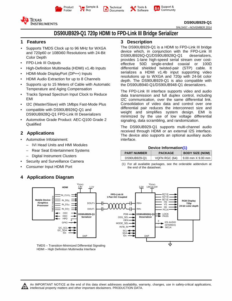
RGB Display720p
24-bit color depth
TM
DS
Inte
rfac
e
Mobile Device/Graphics Processor
FPD-Link III1 Pair / AC Coupled
DS90UB929-Q1Serializer
DS90UB926Q-Q1Deserializer PASS
VDDIO
OSS_SEL
I2C_SCLI2C_SDA
OEN
LOCK
IDxDAP DAP
SCLSDAIDx
R[7:0]
HSVS
PCLKDE
G[7:0]B[7:0]
RIN+
RIN-
DOUT+
DOUT-
1.8V or 3.3V1.8V 1.1V 3.3VVDDIO
I2S AUDIO (STEREO)
3/MODE_SEL
MCLK
PDB
INTB_IN
IN_D0+
IN_D1+
IN_CLK+
IN_D2+
HDMI
4/GPIO
HPDDDCCEC
TMDS ± Transition-Minimized Differential SignalingHDMI ± High Definition Multimedia Interface
Product
Folder
Sample &Buy
Technical
Documents
Tools &
Software
Support &Community
DS90UB929-Q1SNLS457 –NOVEMBER 2014
DS90UB929-Q1 720p HDMI to FPD-Link III Bridge Serializer1 Features 3 Description
The DS90UB929-Q1 is a HDMI to FPD-Link III bridge1• Supports TMDS Clock up to 96 MHz for WXGA
device which, in conjunction with the FPD-Link IIIand 720p60 or 1080i60 Resolutions with 24-BitDS90UB926Q-Q1/DS90UB928Q-Q1 deserializers,Color Depth provides 1-lane high-speed serial stream over cost-
• FPD-Link III Outputs effective 50Ω single-ended coaxial or 100Ωdifferential shielded twisted-pair (STP) cable. It• High-Definition Multimedia (HDMI) v1.4b Inputsserializes a HDMI v1.4b input supporting video• HDMI-Mode DisplayPort (DP++) Inputsresolutions up to WXGA and 720p with 24-bit color
• HDMI Audio Extraction for up to 8 Channels depth. The DS90UB929-Q1 is also compatible with• Supports up to 15 Meters of Cable with Automatic the DS90UB940-Q1/DS90UB948-Q1 deserializers.
Temperature and Aging Compensation The FPD-Link III interface supports video and audio• Tracks Spread Spectrum Input Clock to Reduce data transmission and full duplex control, including
EMI I2C communication, over the same differential link.Consolidation of video data and control over one• I2C (Master/Slave) with 1Mbps Fast-Mode Plusdifferential pair reduces the interconnect size and• compatible with DS90UB926Q-Q1 and weight and simplifies system design. EMI isDS90UB928Q-Q1 FPD-Link III Deserializers minimized by the use of low voltage differential
• Automotive Grade Product: AEC-Q100 Grade 2 signaling, data scrambling, and randomization.Qualified
The DS90UB929-Q1 supports multi-channel audioreceived through HDMI or an external I2S interface.2 Applications The device also supports an optional auxiliary audiointerface.• Automotive Infotainment:
– IVI Head Units and HMI ModulesDevice Information(1)
– Rear Seat Entertainment SystemsPART NUMBER PACKAGE BODY SIZE (NOM)
– Digital Instrument Clusters DS90UB929-Q1 VQFN RGC (64) 9.00 mm X 9.00 mm• Security and Surveillance Camera
(1) For all available packages, see the orderable addendum at• Consumer Input HDMI Port the end of the datasheet.
4 Applications Diagram
1
An IMPORTANT NOTICE at the end of this data sheet addresses availability, warranty, changes, use in safety-critical applications,intellectual property matters and other important disclaimers. PRODUCTION DATA.
DS90UB929-Q1SNLS457 –NOVEMBER 2014 www.ti.com
Table of Contents8.3 Feature Description................................................. 181 Features .................................................................. 18.4 Device Functional Modes........................................ 272 Applications ........................................................... 18.5 Programming........................................................... 293 Description ............................................................. 18.6 Register Maps ......................................................... 324 Applications Diagram ............................................ 1
9 Application and Implementation ........................ 555 Revision History..................................................... 29.1 Applications Information.......................................... 556 Pin Configuration and Functions ......................... 39.2 Typical Applications ................................................ 557 Specifications......................................................... 7 10 Power Supply Recommendations ..................... 607.1 Absolute Maximum Ratings ..................................... 710.1 Power Up Requirements And PDB Pin................. 607.2 Handling Ratings....................................................... 7
11 Layout................................................................... 617.3 Recommended Operating Conditions....................... 711.1 Layout Guidelines ................................................. 617.4 Thermal Information .................................................. 811.2 Layout Example .................................................... 627.5 DC Electrical Characteristics .................................... 9
12 Device and Documentation Support ................. 637.6 AC Electrical Characteristics................................... 1112.1 Documentation Support ....................................... 637.7 DC And AC Serial Control Bus Characteristics ...... 1212.2 Trademarks ........................................................... 637.8 Recommended Timing for the Serial Control Bus .. 1312.3 Electrostatic Discharge Caution............................ 637.9 Typical Characteristics ............................................ 1612.4 Glossary ................................................................ 638 Detailed Description ............................................ 17
13 Mechanical, Packaging and Orderable8.1 Overview ................................................................. 17Information ........................................................... 638.2 Functional Block Diagram ....................................... 17
5 Revision History
DATE REVISION NOTESNovember 2014 * Initial release.
2 Submit Documentation Feedback Copyright © 2014, Texas Instruments Incorporated
Product Folder Links: DS90UB929-Q1

VDD18
VD
DIO
SD
IN /
GP
IO0
RE
S0
IN_D0-
VTERM
IN_D0+
VDDHA11
IN_D1-
IN_D1+
SC
L
VDDHS11
VDD18
RES2
PDB
VD
DA
11
NC
0DOUT-
DOUT+
MC
LK
VDDS11
NC4
NC5
IN_D2-
VDDHA11
CE
C
IN_D2+
VDD18
1 2 3 4 5 6 7 8 9 10 11 12 13 14 15 16
32
31
30
29
28
27
26
25
24
23
22
21
20
19
18
17
48 47 46 45 44 43 42 41 40 39 38 37 36 35 34 33
49
50
51
52
53
54
55
56
57
58
59
60
61
62
63
64
VDDHA11
I2S
_DC
/ G
PIO
2
I2S
_DD
/ G
PIO
3
VDDHA11
LFT
MODE_SEL0
IDx
RX
_5V
IN_CLK-
IN_CLK+
VD
DL1
1
X1
RE
M_I
NT
B
SC
LK /
I2C
SE
L
VD
DL1
1
RES1
VDDHS11
DD
C_S
DA
NC
7
DD
C_S
CL
NC
6
SD
A
INT
B
NC
3
NC
2
I2S
_WC
/ G
PIO
7_R
EG
I2S
_DB
/ G
PIO
5_R
EG
I2S
_CLK
/ G
PIO
8_R
EG
I2S
_DA
/ G
PIO
6_R
EG
NC
1
MODE_SEL1
NC8
HP
D
SW
C /
GP
IO1
DS90UB929-Q1
DAP = GND
VDDP11
VD
DIO
64 VQFNTop View
DS90UB929-Q1www.ti.com SNLS457 –NOVEMBER 2014
6 Pin Configuration and Functions
64 PINSTop View
Pin FunctionsPIN
I/O, TYPE DESCRIPTIONNAME NO.HDMI TMDS INPUTIN_CLK- 49 I, TMDS TMDS Clock Differential InputIN_CLK+ 50IN_D0- 55 I, TMDS TMDS Data Channel 0 Differential InputIN_D0+ 56IN_D1- 59 I, TMDS TMDS Data Channel 1 Differential InputIN_D1+ 60IN_D2- 62 I, TMDS TMDS Data Channel 2 Differential InputIN_D2+ 63OTHER HDMIHPD 42 O, Open- Hot Plug Detect Output. Pull up to RX_5V with a 1kΩ resistor
DrainRX_5V 43 I HDMI 5V Detect InputDDC_SDA 44 IO, Open- DDC Slave Serial Data
Drain Pull up to RX_5V with a 47kΩ resistorDDC_SCL 45 I, Open-Drain DDC Slave Serial Clock
Pull up to RX_5V with a 47kΩ resistor
Copyright © 2014, Texas Instruments Incorporated Submit Documentation Feedback 3
Product Folder Links: DS90UB929-Q1
DS90UB929-Q1SNLS457 –NOVEMBER 2014 www.ti.com
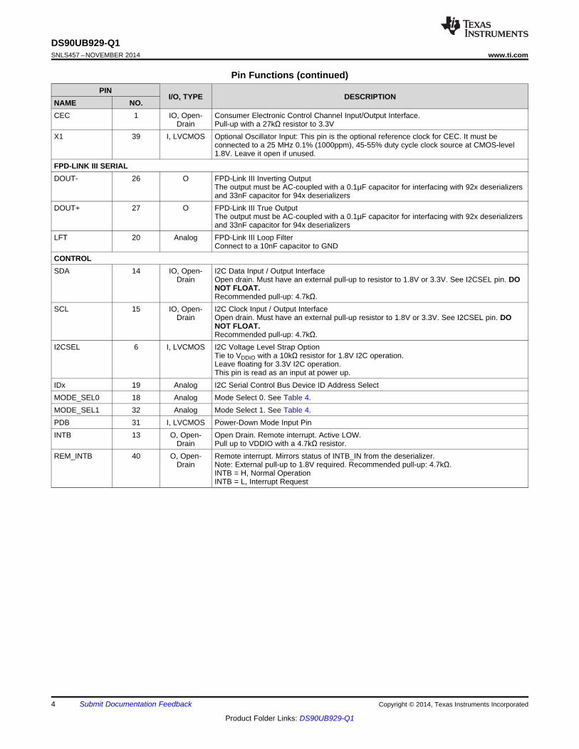
Pin Functions (continued)PIN
I/O, TYPE DESCRIPTIONNAME NO.CEC 1 IO, Open- Consumer Electronic Control Channel Input/Output Interface.
Drain Pull-up with a 27kΩ resistor to 3.3VX1 39 I, LVCMOS Optional Oscillator Input: This pin is the optional reference clock for CEC. It must be
connected to a 25 MHz 0.1% (1000ppm), 45-55% duty cycle clock source at CMOS-level1.8V. Leave it open if unused.
FPD-LINK III SERIALDOUT- 26 O FPD-Link III Inverting Output
The output must be AC-coupled with a 0.1µF capacitor for interfacing with 92x deserializersand 33nF capacitor for 94x deserializers
DOUT+ 27 O FPD-Link III True OutputThe output must be AC-coupled with a 0.1µF capacitor for interfacing with 92x deserializersand 33nF capacitor for 94x deserializers
LFT 20 Analog FPD-Link III Loop FilterConnect to a 10nF capacitor to GND
CONTROLSDA 14 IO, Open- I2C Data Input / Output Interface
Drain Open drain. Must have an external pull-up to resistor to 1.8V or 3.3V. See I2CSEL pin. DONOT FLOAT.Recommended pull-up: 4.7kΩ.
SCL 15 IO, Open- I2C Clock Input / Output InterfaceDrain Open drain. Must have an external pull-up resistor to 1.8V or 3.3V. See I2CSEL pin. DO
NOT FLOAT.Recommended pull-up: 4.7kΩ.
I2CSEL 6 I, LVCMOS I2C Voltage Level Strap OptionTie to VDDIO with a 10kΩ resistor for 1.8V I2C operation.Leave floating for 3.3V I2C operation.This pin is read as an input at power up.
IDx 19 Analog I2C Serial Control Bus Device ID Address SelectMODE_SEL0 18 Analog Mode Select 0. See Table 4.MODE_SEL1 32 Analog Mode Select 1. See Table 4.PDB 31 I, LVCMOS Power-Down Mode Input PinINTB 13 O, Open- Open Drain. Remote interrupt. Active LOW.
Drain Pull up to VDDIO with a 4.7kΩ resistor.REM_INTB 40 O, Open- Remote interrupt. Mirrors status of INTB_IN from the deserializer.
Drain Note: External pull-up to 1.8V required. Recommended pull-up: 4.7kΩ.INTB = H, Normal OperationINTB = L, Interrupt Request
4 Submit Documentation Feedback Copyright © 2014, Texas Instruments Incorporated
Product Folder Links: DS90UB929-Q1

DS90UB929-Q1www.ti.com SNLS457 –NOVEMBER 2014
Pin Functions (continued)PIN
I/O, TYPE DESCRIPTIONNAME NO.BIDIRECTIONAL CONTROL CHANNEL (BCC) GPIO PINSGPIO0 4 IO, LVCMOS BCC GPIO0. Shared with SDINGPIO1 5 IO, LVCMOS BCC GPIO1. Shared with SWCGPIO2 37 IO, LVCMOS BCC GPIO2. Shared with I2S_DCGPIO3 38 IO, LVCMOS BCC GPIO3. Shared with I2S_DDREGISTER-ONLY GPIOGPIO5_REG 36 IO, LVCMOS General Purpose Input/Output 5
Local register control only. Shared with I2S_DBGPIO6_REG 35 IO, LVCMOS General Purpose Input/Output 6
Local register control only. Shared with I2S_DAGPIO7_REG 33 IO, LVCMOS General Purpose Input/Output 7
Local register control only. Shared with I2S_WCGPIO8_REG 34 IO, LVCMOS General Purpose Input/Output 8
Local register control only. Shared with I2S_CLKSLAVE MODE LOCAL I2S CHANNEL PINSI2S_WC 33 I, LVCMOS Slave Mode I2S Word Clock Input. Shared with GPIO7_REGI2S_CLK 34 I, LVCMOS Slave Mode I2S Clock Input. Shared with GPIO8_REGI2S_DA 35 I, LVCMOS Slave Mode I2S Data Input. Shared with GPIO6_REGI2S_DB 36 I, LVCMOS Slave Mode I2S Data Input. Shared with GPIO5_REGI2S_DC 37 I, LVCMOS Slave Mode I2S Data Input. Shared with GPIO2I2S_DD 38 I, LVCMOS Slave Mode I2S Data Input. Shared with GPIO3AUXILIARY I2S CHANNEL PINSSWC 5 O, LVCMOS Master Mode I2S Word Clock Ouput. Shared with GPIO1SCLK 6 O, LVCMOS Master Mode I2S Clock Ouput. Shared with I2CSEL. This pin is sampled following power-up
as I2CSEL, then it will switch to SCLK operation as an output.SDIN 4 I, LVCMOS Master Mode I2S Data Input. Shared with GPIO0MCLK 16 IO, LVCMOS Master Mode I2S System Clock Input/OutputPOWER and GROUNDVTERM 57 Power 3.3V (±5%) Supply for DC-coupled internal termination OR
1.8V (±5%) Supply for AC-coupled internal terminationRefer to Figure 22 or Figure 21.
VDD18 24 Power 1.8 (±5%) Analog supply. Refer to Figure 22 or Figure 21.5164
VDDA11 9 Power 1.1V(±5%) Analog supply. Refer to Figure 22 or Figure 21.VDDHA11 52 Power 1.1V(±5%) TMDS supply. Refer to Figure 22 or Figure 21.
545861
VDDHS11 21 Power 1.1V(±5%) supply. Refer to Figure 22 or Figure 21.28
VDDL11 7 Power 1.1V(±5%) Digital supply. Refer to Figure 22 or Figure 21.41
VDDP11 17 Power 1.1V(±5%) PLL supply. Refer to Figure 22 or Figure 21.VDDS11 25 Power 1.1V(±5%) Serializer supply. Refer to Figure 22 or Figure 21.VDDIO 3 Power 1.8V (±5%) IO supply. Refer to Figure 22 or Figure 21.
46GND Thermal GND Ground. Connect to Ground plane with at least 9 vias.
PadOTHERRES0 2 Reserved. Tie to GND.RES1 29
Copyright © 2014, Texas Instruments Incorporated Submit Documentation Feedback 5
Product Folder Links: DS90UB929-Q1

DS90UB929-Q1SNLS457 –NOVEMBER 2014 www.ti.com
Pin Functions (continued)PIN
I/O, TYPE DESCRIPTIONNAME NO.RES2 30 Reserved. Connect with 50Ω to GND.NC0 8 No connect. Leave floating. Do not connect to VDD or GND.NC1 10NC2 11NC3 12NC4 22NC5 23NC6 47NC7 48NC8 53
6 Submit Documentation Feedback Copyright © 2014, Texas Instruments Incorporated
Product Folder Links: DS90UB929-Q1

DS90UB929-Q1www.ti.com SNLS457 –NOVEMBER 2014
7 Specifications
7.1 Absolute Maximum RatingsMIN MAX UNIT
Supply Voltage – VDD11 −0.3 1.7 VSupply Voltage – VDD18 -0.3 2.5 VSupply Voltage – VDDIO −0.3 2.5 VOpenLDI Inputs -0.3 2.75 VLVCMOS I/O Voltage −0.3 (VDDIO + 0.3) V1.8V Tolerant I/O -0.3 2.5 V3.3V Tolerant I/O -0.3 4.0 V5V Tolerant I/O -0.3 5.3 VFPD-Link III Output Voltage −0.3 1.7 VJunction Temperature 150 °CFor soldering specifications:
see product folder at www.ti.com and www.ti.com/lit/an/snoa549c/snoa549c.pdf
7.2 Handling RatingsMIN MAX UNIT
Tstg Storage temperature range 64 Lead VQFN Package -65 +150 °CHuman body model (HBM), per AEC Q100-002 (1) -2 +2 kV
V(ESD) Electrostatic dischargeCharged device model (CDM), per AEC Q100-011 -750 +750 VAir Discharge (DOUT+, DOUT-) -15 +15ESD Rating (IEC 61000-4-2) kVRD = 330Ω, CS = 150pF Contact Discharge (DOUT+, DOUT-) -8 +8
ESD Rating (ISO10605) Air Discharge (DOUT+, DOUT-) -15 +15RD = 330Ω, CS = 150pF kV
Contact Discharge (DOUT+, DOUT-) -8 +8RD = 2KΩ, CS = 150pF or 330pF
(1) AEC Q100-002 indicates HBM stressing is done in accordance with the ANSI/ESDA/JEDEC JS-001 specification.
7.3 Recommended Operating ConditionsMIN NOM MAX UNIT
Supply Voltage (VDD11) 1.045 1.1 1.155 VSupply Voltage (VDD18) 1.71 1.8 1.89 VLVCMOS Supply Voltage (VDDIO) 1.71 1.8 1.89 VVDDI2C, 1.8V Operation 1.71 1.8 1.89 VVDDI2C, 3.3V Operation 3.135 3.3 3.465 VHDMI Termination (VTERM), DC-coupled 3.135 3.3 3.465 VHDMI Termination (VTERM), AC-coupled 1.71 1.8 1.89 VOperating Free Air Temperature (TA) −40 +25 +105 °CTMDS Frequency 25 96 MHz
Copyright © 2014, Texas Instruments Incorporated Submit Documentation Feedback 7
Product Folder Links: DS90UB929-Q1

DS90UB929-Q1SNLS457 –NOVEMBER 2014 www.ti.com
7.4 Thermal InformationVQFN
THERMAL METRIC (1) UNIT64 PINS
RθJA Junction-to-ambient thermal resistance 25.8RθJC(top) Junction-to-case (top) thermal resistance 11.4RθJB Junction-to-board thermal resistance 5.1
°C/WψJT Junction-to-top characterization parameter 0.2ψJB Junction-to-board characterization parameter 5.1RθJC(bot) Junction-to-case (bottom) thermal resistance 0.8
(1) For more information about traditional and new thermal metrics, see the IC Package Thermal Metrics application report, SPRA953.
8 Submit Documentation Feedback Copyright © 2014, Texas Instruments Incorporated
Product Folder Links: DS90UB929-Q1

DS90UB929-Q1www.ti.com SNLS457 –NOVEMBER 2014
7.5 DC Electrical CharacteristicsOver recommended operating supply and temperature ranges unless otherwise specified.
PARAMETER TEST CONDITIONS PIN/FREQ. MIN TYP MAX UNIT1.8V LVCMOS I/O
High Level Input SCLK/I2CSEL,VIH 0.65 * VDDIO VVoltage PDB, SDIN/GPIO0,SWC/GPIO1,Low Level InputVIL 0 0.35 * VDDIO VMCLKVoltage I2S_DC/GPIO2,I2S_DD/GPIO3,I2S_DB/GPIO5_REG,I2S_DA/GPIO6_RE
IIN Input Current VIN = 0V or 1.89V −10 10 μAG,I2S_CLK/GPIO8_REG,I2S_WC/GPIO7_REG
High Level OutputVOH IOH = −4mA 0.7 * VDDIO VDDIO VVoltageLow Level OutputVOL IOL = +4mA GND 0.26 * VDDIO VVoltage
Same as aboveOutput Short CircuitIOS VOUT = 0V -50 mACurrentTRI-STATE™ OutputIOZ VOUT = 0V or VDDIO, PDB = L −10 10 μACurrent
TMDS INPUTS -- FROM HDMI v1.4b SECTION 4.2.5Input Common-Mode IN_D[2:0]+,VICM1 VTERM - 300 VTERM - 37.5 mVVoltage IN_D[2:0]-Input Common-Mode IN_CLK+, IN_CLK-VICM2 IN_CLK ≤ 96MHz VTERM - 10 VTERM + 10 mVVoltage VTERM = 1.8V (+,-
5%) or VTERM =Input DifferentialVIDIFF 150 1200 mVP-P3.3V (+,- 5%)Voltage LevelIN_D[2:0]+,TerminationRTMDS Differential IN_D[2:0]- 90 100 110 ΩResistance IN_CLK+, IN_CLK-
HDMI IO -- FROM HDMI v1.4b SECTION 4.2.7 to 4.2.94.8 5.3 VVRX_5V +5V Power Signal
RX_5V50 mAI5V_Sink +5V Input Current
High Level OutputVOH,HPD IOH = -4mA 2.4 5.3 VVoltage, HPDHPD, RPU = 1 kΩ
Low Level OutputVOL,HPD IOL = +4mA GND 0.4 VVoltage, HPDPower-Down InputIIZ,HPD PDB = L -10 10 uACurrent, HPDLow Level InputVIL,DDC 0.3*VDD,DDC VVoltage, DDCHigh Level Input DDC_SCL,VIH,DDC 0.7*VDD,DDC VVoltage, DDC DDC_SDAPower-Down InputIIZ,DDC PDB = L -10 10 µACurrent, DDC
Copyright © 2014, Texas Instruments Incorporated Submit Documentation Feedback 9
Product Folder Links: DS90UB929-Q1
DS90UB929-Q1SNLS457 –NOVEMBER 2014 www.ti.com
DC Electrical Characteristics (continued)Over recommended operating supply and temperature ranges unless otherwise specified.
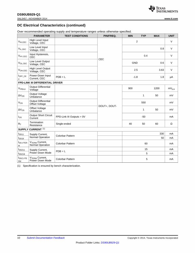
PARAMETER TEST CONDITIONS PIN/FREQ. MIN TYP MAX UNITHigh Level InputVIH,CEC 2 VVoltage, CECLow Level InputVIL,CEC 0.8 VVoltage, CECInput Hysteresis,VHY,CEC 0.4 VCEC
CECLow Level OutputVOL,CEC GND 0.6 VVoltage, CECHigh Level OutputVOH,CEC 2.5 3.63 VVoltage, CEC
IOFF_CE Power-Down Input PDB = L -1.8 1.8 µAC Current, CECFPD-LINK III DIFFERENTIAL DRIVER
Output DifferentialVODp-p 900 1200 mVp-pVoltageOutput VoltageΔVOD 1 50 mVUnbalanceOutput DifferentialVOS 550 mVOffset Voltage
DOUT+, DOUT-Offset VoltageΔVOS 1 50 mVUnbalanceOutput Short CircuitIOS FPD-Link III Outputs = 0V -50 mACurrentTerminationRT Single-ended 40 50 60 ΩResistance
SUPPLY CURRENT (1)
IDD11 330 mASupply Current, Colorbar PatternNormal OperationIDD18 50 mAIDD,VTER VTERM Current, Colorbar Pattern 60 mAM Normal OperationIDDZ11 15 mASupply Current, PDB = LPower Down ModeIDDZ18 5 mAIDDZ,VTE VTERM Current, Colorbar Pattern 5 mARM Power Down Mode
(1) Specification is ensured by bench characterization.
10 Submit Documentation Feedback Copyright © 2014, Texas Instruments Incorporated
Product Folder Links: DS90UB929-Q1
DS90UB929-Q1www.ti.com SNLS457 –NOVEMBER 2014
7.6 AC Electrical CharacteristicsOver recommended operating supply and temperature ranges unless otherwise specified.
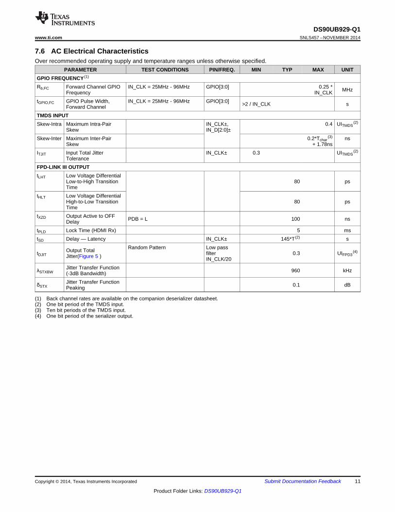
PARAMETER TEST CONDITIONS PIN/FREQ. MIN TYP MAX UNITGPIO FREQUENCY (1)
Rb,FC Forward Channel GPIO IN_CLK = 25MHz - 96MHz GPIO[3:0] 0.25 * MHzFrequency IN_CLKtGPIO,FC GPIO Pulse Width, IN_CLK = 25MHz - 96MHz GPIO[3:0] >2 / IN_CLK sForward ChannelTMDS INPUTSkew-Intra Maximum Intra-Pair IN_CLK±, 0.4 UITMDS
(2)
Skew IN_D[2:0]±Skew-Inter Maximum Inter-Pair 0.2*Tchar
(3) nsSkew + 1.78ns
ITJIT Input Total Jitter IN_CLK± 0.3 UITMDS(2)
ToleranceFPD-LINK III OUTPUTtLHT Low Voltage Differential
Low-to-High Transition 80 psTime
tHLT Low Voltage DifferentialHigh-to-Low Transition 80 psTime
tXZD Output Active to OFF PDB = L 100 nsDelaytPLD Lock Time (HDMI Rx) 5 mstSD Delay — Latency IN_CLK± 145*T (2) s
Random Pattern Low passOutput TotaltDJIT filter 0.3 UIFPD3(4)
Jitter(Figure 5 ) IN_CLK/20Jitter Transfer FunctionλSTXBW 960 kHz(-3dB Bandwidth)Jitter Transfer FunctionδSTX 0.1 dBPeaking
(1) Back channel rates are available on the companion deserializer datasheet.(2) One bit period of the TMDS input.(3) Ten bit periods of the TMDS input.(4) One bit period of the serializer output.
Copyright © 2014, Texas Instruments Incorporated Submit Documentation Feedback 11
Product Folder Links: DS90UB929-Q1

DS90UB929-Q1SNLS457 –NOVEMBER 2014 www.ti.com
7.7 DC And AC Serial Control Bus CharacteristicsOver VDDI2C supply and temperature ranges unless otherwise specified. VDDI2C can be 1.8V (+,- 5%) or 3.3V (+,- 5%) (refer toI2CSEL pin description for 1.8V or 3.3V operation).
PARAMETER TEST CONDITIONS MIN TYP MAX UNITVIH,I2C 0.7*SDA and SCL, VDDI2C = 1.8V VVDDI2CInput High Level, I2C
0.7*SDA and SCL, VDDI2C = 3.3V VVDDI2C
VIL,I2C 0.3*SDA and SCL, VDDI2C = 1.8V VVDDI2CInput Low Level Voltage, I2C0.3*SDA and SCL, VDDI2C = 3.3V VVDDI2C
VHY Input Hysteresis, I2C SDA and SCL, VDDI2C = 1.8V or 3.3V >50 mVVOL,I2C Output Low Level, I2C SDA and SCL, VDDI2C = 1.8V, Fast-Mode, 3mA Sink 0.2 *GND VCurrent VDDI2C
SDA and SCL, VDDI2C = 3.3V, 3mA Sink Current GND 0.4 VIIN,I2C Input Current, I2C SDA and SCL, VDDI2C = 0V -800 -600 µA
SDA and SCL, VDDI2C = VDD18 or VDD33 -10 +10 µACIN,I2C Input Capacitance, I2C SDA and SCL 5 pF
12 Submit Documentation Feedback Copyright © 2014, Texas Instruments Incorporated
Product Folder Links: DS90UB929-Q1
DS90UB929-Q1www.ti.com SNLS457 –NOVEMBER 2014
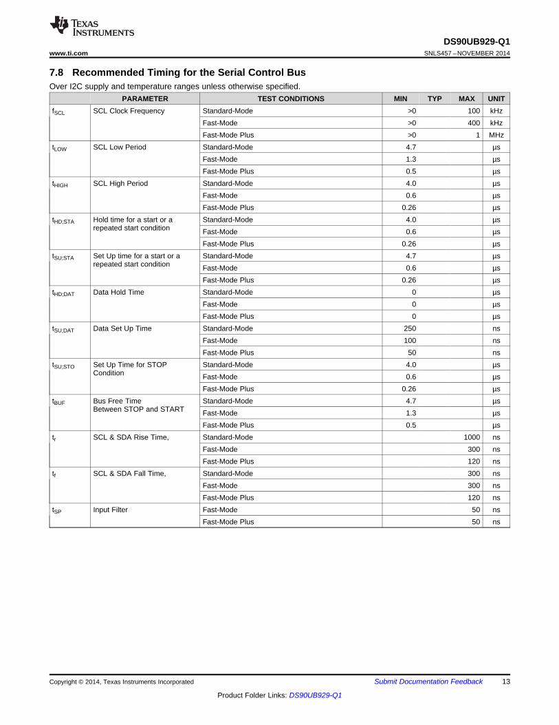
7.8 Recommended Timing for the Serial Control BusOver I2C supply and temperature ranges unless otherwise specified.
PARAMETER TEST CONDITIONS MIN TYP MAX UNITfSCL SCL Clock Frequency Standard-Mode >0 100 kHz
Fast-Mode >0 400 kHzFast-Mode Plus >0 1 MHz
tLOW SCL Low Period Standard-Mode 4.7 µsFast-Mode 1.3 µsFast-Mode Plus 0.5 µs
tHIGH SCL High Period Standard-Mode 4.0 µsFast-Mode 0.6 µsFast-Mode Plus 0.26 µs
tHD;STA Hold time for a start or a Standard-Mode 4.0 µsrepeated start condition Fast-Mode 0.6 µs
Fast-Mode Plus 0.26 µstSU;STA Set Up time for a start or a Standard-Mode 4.7 µs
repeated start condition Fast-Mode 0.6 µsFast-Mode Plus 0.26 µs
tHD;DAT Data Hold Time Standard-Mode 0 µsFast-Mode 0 µsFast-Mode Plus 0 µs
tSU;DAT Data Set Up Time Standard-Mode 250 nsFast-Mode 100 nsFast-Mode Plus 50 ns
tSU;STO Set Up Time for STOP Standard-Mode 4.0 µsCondition Fast-Mode 0.6 µs
Fast-Mode Plus 0.26 µstBUF Bus Free Time Standard-Mode 4.7 µs
Between STOP and START Fast-Mode 1.3 µsFast-Mode Plus 0.5 µs
tr SCL & SDA Rise Time, Standard-Mode 1000 nsFast-Mode 300 nsFast-Mode Plus 120 ns
tf SCL & SDA Fall Time, Standard-Mode 300 nsFast-Mode 300 nsFast-Mode Plus 120 ns
tSP Input Filter Fast-Mode 50 nsFast-Mode Plus 50 ns
Copyright © 2014, Texas Instruments Incorporated Submit Documentation Feedback 13
Product Folder Links: DS90UB929-Q1
RX_5V
IN_CLK (Diff.)
DOUT(Diff.)
Driver OFF, VOD = 0V Driver On
VDDVDDIO
tPLD
PDB
0V
tHLTtLHT
(DOUT+) - (DOUT-)
20%
80%
VOD
DOUT+
0V
0V
VOD/2
VOD
Single Ended
Differential
VOS
DOUT-
(DOUT+) - (DOUT-)
|
PA
RA
LLE
L-T
O-S
ER
IAL
IN_CLK±IN_D[2:0]±
100:
DOUT-
DOUT+
D
100 nF
100 nF
SCOPEBW û 4GHz
Differential probeInput Impedance û 100 k:
CL ú 0.5 pfBW û 3.5 GHz
VOD/2
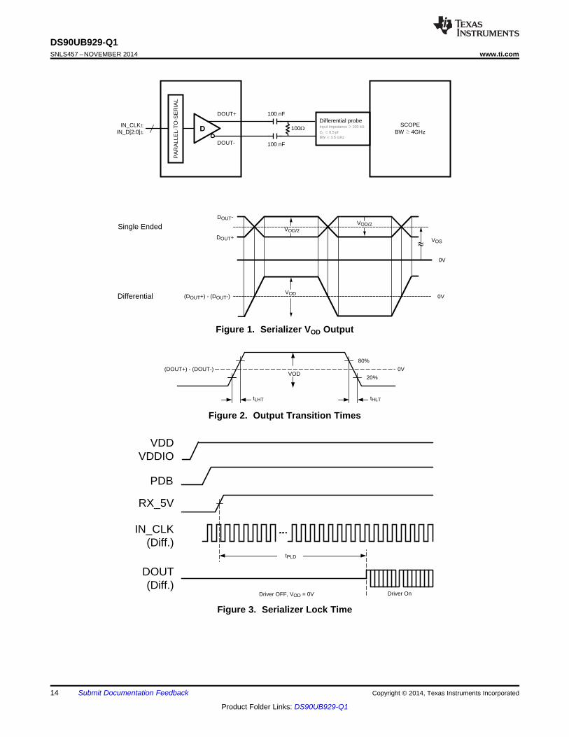
DS90UB929-Q1SNLS457 –NOVEMBER 2014 www.ti.com
Figure 1. Serializer VOD Output
Figure 2. Output Transition Times
Figure 3. Serializer Lock Time
14 Submit Documentation Feedback Copyright © 2014, Texas Instruments Incorporated
Product Folder Links: DS90UB929-Q1
I2S_WCI2S_D[A,B,C,D]
I2S_CLK
VIH
VIL
tHCtLC
tsr thr
T
SCL
SDA
tHD;STA
tLOW
tr
tHD;DAT
tHIGH
tf
tSU;DAT
tSU;STA tSU;STO
tf
START REPEATEDSTART
STOP
tHD;STA
START
tSP
trBUFt
DOUT(Diff.)
tDJIT
tBIT (1 UI)
EYE OPENING 0V
tDJIT
210
||
STARTBIT
STOPBITSYMBOL N
210
||
STARTBIT
STOPBITSYMBOL N-1
210
||
STARTBIT
STOPBITSYMBOL N-2
210
||
STARTBIT
STOPBITSYMBOL N-3
210
STOPBITSYMBOL N-4
||
DOUT
|
IN_CLK
tSD
NN-1 N+1 N+2
||
IN_D[2:0]
DS90UB929-Q1www.ti.com SNLS457 –NOVEMBER 2014
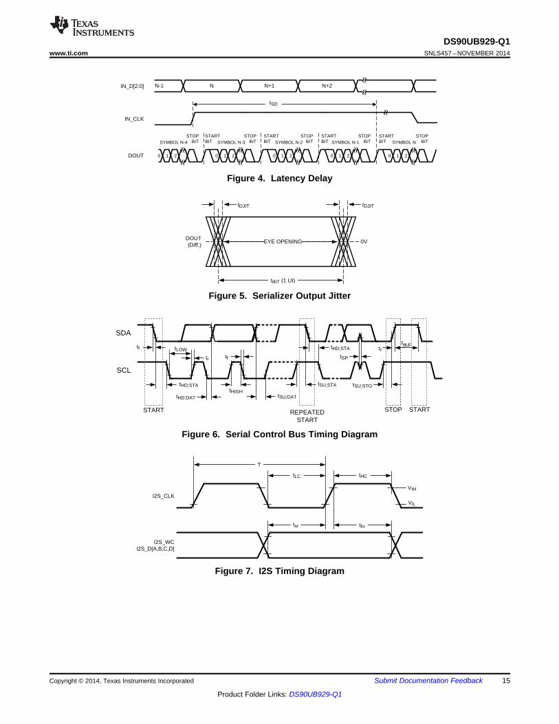
Figure 4. Latency Delay
Figure 5. Serializer Output Jitter
Figure 6. Serial Control Bus Timing Diagram
Figure 7. I2S Timing Diagram
Copyright © 2014, Texas Instruments Incorporated Submit Documentation Feedback 15
Product Folder Links: DS90UB929-Q1
DS90UB929-Q1SNLS457 –NOVEMBER 2014 www.ti.com
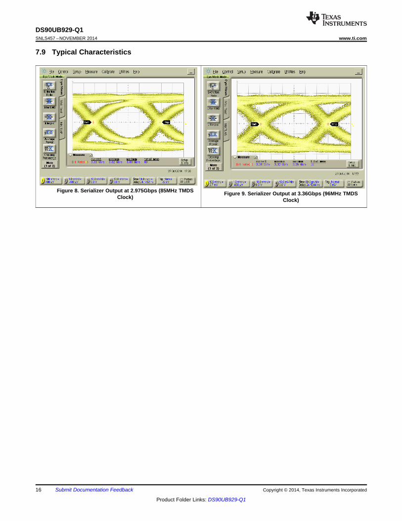
7.9 Typical Characteristics
Figure 8. Serializer Output at 2.975Gbps (85MHz TMDS Figure 9. Serializer Output at 3.36Gbps (96MHz TMDSClock) Clock)
16 Submit Documentation Feedback Copyright © 2014, Texas Instruments Incorporated
Product Folder Links: DS90UB929-Q1

FPD-Link III Digital
HDMI ControllerDigital
HDMI RXPHY
FPD-Link III TXDigital
FPD3 TXAnalog
Bridge ControlDigital
TMDS
DDC
HPA
FPD-Link III
Audio PLL
AudioFIFO
PacketFIFO
EDID/ConfigNVM
EDIDI/F
I2S Audio
Video
RX_5V
I2C OptionalSecondary
I2S
DigitalTMDS
Interface
FPD-Link III TXDigital
PATGEN
HDCP
HDCP
DS90UB929-Q1www.ti.com SNLS457 –NOVEMBER 2014
8 Detailed Description
8.1 OverviewThe DS90UB929-Q1 converts an HDMI interface (3 TMDS data channels + 1 TMDS Clock) to an FPD-Link IIIinterface. This device transmits a 35-bit symbol over a single serial pair operating up to 3.36Gbps line rate. Theserial stream contains an embedded clock, video control signals, RGB video data, and audio data. The payloadis DC-balanced to enhance signal quality and support AC coupling.
The DS90UB929-Q1 serializer is intended for use with a DS90UB926Q-Q1, DS90UB928Q-Q1, DS90UB940-Q1,DS90UB948-Q1 deserializer.
The DS90UB929-Q1 serializer and companion deserializer incorporate an I2C compatible interface. The I2Ccompatible interface allows programming of serializer or deserializer devices from a local host controller. Inaddition, the devices incorporate a bidirectional control channel (BCC) that allows communication betweenserializer/deserializer as well as remote I2C slave devices.
The bidirectional control channel (BCC) is implemented via embedded signaling in the high-speed forwardchannel (serializer to deserializer) combined with lower speed signaling in the reverse channel (deserializer toserializer). Through this interface, the BCC provides a mechanism to bridge I2C transactions across the seriallink from one I2C bus to another. The implementation allows for arbitration with other I2C compatible masters ateither side of the serial link.
8.2 Functional Block Diagram
Copyright © 2014, Texas Instruments Incorporated Submit Documentation Feedback 17
Product Folder Links: DS90UB929-Q1

DS90UB929-Q1SNLS457 –NOVEMBER 2014 www.ti.com
8.3 Feature Description
8.3.1 High-Definition Multimedia Interface (HDMI)HDMI is a leading interface standard used to transmit digital video and audio from sources (such as a DVDplayer) to sinks (such as an LCD display). The interface is capable of transmitting high-definition video and audio.Other HDMI signals consist of various control and status data that travel bidirectionally.
8.3.1.1 HDMI Receive ControllerThe HDMI Receiver is an HDMI version 1.4b compliant receiver. The HDMI receiver is capable of operation atgreater than 1080p resolutions. The DS90UB929-Q1 implementation is restricted to 720p operation (or 1080i or1080p/30).The configuration used in the DS90UB929-Q1does not include version 1.4b features such as theethernet channel (HEC) or Audio Return Channel (ARC).
8.3.2 Transition Minimized Differential SignalingHDMI uses Transition Minimized Differential Signaling (TMDS) over four differential pairs (3 TMDS channels and1 TMDS clock) to transmit video and audio data. TMDS is widely used to transmit high-speed serial data. Thetechnology incorporates a form of 8b/10b encoding and its differential signaling allows it to reduceelectromagnetic interference (EMI) and achieve high skew tolerance.
8.3.3 Enhanced Display Data ChannelThe Display Data Channel or DDC is a collection of digital communication protocols between a computer displayand a graphics adapter that enables the display to communicate its supported display modes to the adapter andallow the computer host to adjust monitor parameters, such as brightness and contrast.
8.3.4 Extended Display Identification Data (EDID)EDID is a data structure provided by a digital display to describe its capabilities to a video source. By providingthis information, the video source can then send video data with proper timing and resolution that the displaysupports. The DS90UB929-Q1 supports several options for delivering display identification (EDID) information tothe HDMI graphics source. The EDID information is accessible via the DDC interface and comply with the DDCand EDID requirements given in the HDMI v1.4b specification.
The EDID configurations supported are as follows:• External local EDID (EEPROM)• Internal EDID loaded into device memory• Remote EDID connected to I2C bus at deserializer side• Internal pre-programmed EDID
The EDID mode selected should be configurable from the MODE_SEL pins, or from internal control registers. Forall modes, the EDID information should be accessible at the default address of 0xA0.
8.3.4.1 External Local EDID (EEPROM)The DS90UB929-Q1 can be configured to allow a local EEPROM EDID device. The local EDID device mayimplement any EDID configuration allowable by the HDMI v1.4b and DVI 1.0 standards, including multipleextension blocks up to 32KB.
8.3.4.2 Internal EDID (SRAM)The DS90UB929-Q1 also allows internal loading of an EDID profile up to 256 bytes. This SRAM storage isvolatile and requires loading from an external I2C master (local or remote). The internal EDID is reloadable andreadable (local/remote) from control registers during normal operation.
8.3.4.3 External Remote EDIDThe serializer copies the remote EDID connected to the I2C bus of the remote deserializer into its internalSRAM. The remote EDID device can be a standalone I2C EEPROM, or integrated into the digital display panel.In this mode, the serializer automatically accesses the Bidirectional Control Channel to search for the EDIDinformation at the default address 0xA0. Once found, the serializer copies the remote EDID into local SRAM.
18 Submit Documentation Feedback Copyright © 2014, Texas Instruments Incorporated
Product Folder Links: DS90UB929-Q1
C1 C0
DS90UB929-Q1www.ti.com SNLS457 –NOVEMBER 2014
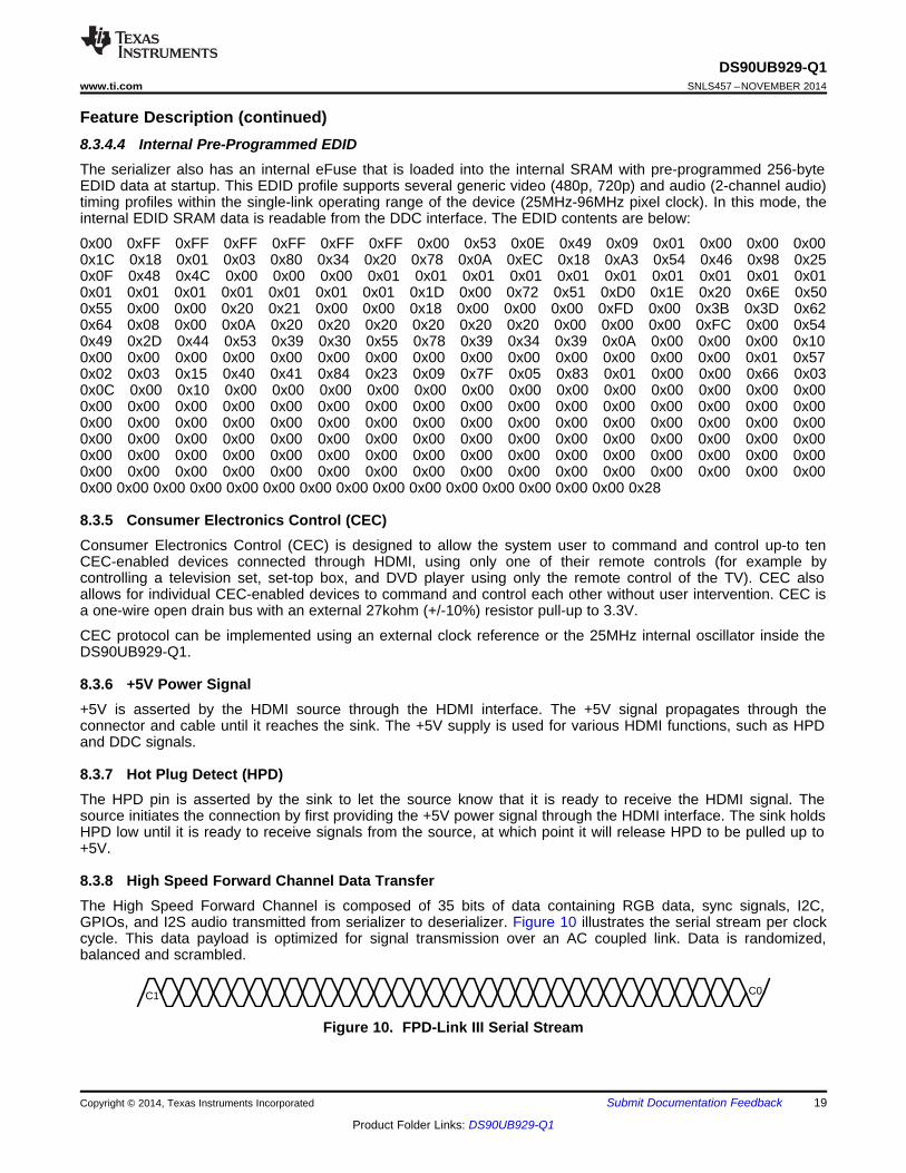
Feature Description (continued)8.3.4.4 Internal Pre-Programmed EDIDThe serializer also has an internal eFuse that is loaded into the internal SRAM with pre-programmed 256-byteEDID data at startup. This EDID profile supports several generic video (480p, 720p) and audio (2-channel audio)timing profiles within the single-link operating range of the device (25MHz-96MHz pixel clock). In this mode, theinternal EDID SRAM data is readable from the DDC interface. The EDID contents are below:
0x00 0xFF 0xFF 0xFF 0xFF 0xFF 0xFF 0x00 0x53 0x0E 0x49 0x09 0x01 0x00 0x00 0x000x1C 0x18 0x01 0x03 0x80 0x34 0x20 0x78 0x0A 0xEC 0x18 0xA3 0x54 0x46 0x98 0x250x0F 0x48 0x4C 0x00 0x00 0x00 0x01 0x01 0x01 0x01 0x01 0x01 0x01 0x01 0x01 0x010x01 0x01 0x01 0x01 0x01 0x01 0x01 0x1D 0x00 0x72 0x51 0xD0 0x1E 0x20 0x6E 0x500x55 0x00 0x00 0x20 0x21 0x00 0x00 0x18 0x00 0x00 0x00 0xFD 0x00 0x3B 0x3D 0x620x64 0x08 0x00 0x0A 0x20 0x20 0x20 0x20 0x20 0x20 0x00 0x00 0x00 0xFC 0x00 0x540x49 0x2D 0x44 0x53 0x39 0x30 0x55 0x78 0x39 0x34 0x39 0x0A 0x00 0x00 0x00 0x100x00 0x00 0x00 0x00 0x00 0x00 0x00 0x00 0x00 0x00 0x00 0x00 0x00 0x00 0x01 0x570x02 0x03 0x15 0x40 0x41 0x84 0x23 0x09 0x7F 0x05 0x83 0x01 0x00 0x00 0x66 0x030x0C 0x00 0x10 0x00 0x00 0x00 0x00 0x00 0x00 0x00 0x00 0x00 0x00 0x00 0x00 0x000x00 0x00 0x00 0x00 0x00 0x00 0x00 0x00 0x00 0x00 0x00 0x00 0x00 0x00 0x00 0x000x00 0x00 0x00 0x00 0x00 0x00 0x00 0x00 0x00 0x00 0x00 0x00 0x00 0x00 0x00 0x000x00 0x00 0x00 0x00 0x00 0x00 0x00 0x00 0x00 0x00 0x00 0x00 0x00 0x00 0x00 0x000x00 0x00 0x00 0x00 0x00 0x00 0x00 0x00 0x00 0x00 0x00 0x00 0x00 0x00 0x00 0x000x00 0x00 0x00 0x00 0x00 0x00 0x00 0x00 0x00 0x00 0x00 0x00 0x00 0x00 0x00 0x000x00 0x00 0x00 0x00 0x00 0x00 0x00 0x00 0x00 0x00 0x00 0x00 0x00 0x00 0x00 0x28
8.3.5 Consumer Electronics Control (CEC)Consumer Electronics Control (CEC) is designed to allow the system user to command and control up-to tenCEC-enabled devices connected through HDMI, using only one of their remote controls (for example bycontrolling a television set, set-top box, and DVD player using only the remote control of the TV). CEC alsoallows for individual CEC-enabled devices to command and control each other without user intervention. CEC isa one-wire open drain bus with an external 27kohm (+/-10%) resistor pull-up to 3.3V.
CEC protocol can be implemented using an external clock reference or the 25MHz internal oscillator inside theDS90UB929-Q1.
8.3.6 +5V Power Signal+5V is asserted by the HDMI source through the HDMI interface. The +5V signal propagates through theconnector and cable until it reaches the sink. The +5V supply is used for various HDMI functions, such as HPDand DDC signals.
8.3.7 Hot Plug Detect (HPD)The HPD pin is asserted by the sink to let the source know that it is ready to receive the HDMI signal. Thesource initiates the connection by first providing the +5V power signal through the HDMI interface. The sink holdsHPD low until it is ready to receive signals from the source, at which point it will release HPD to be pulled up to+5V.
8.3.8 High Speed Forward Channel Data TransferThe High Speed Forward Channel is composed of 35 bits of data containing RGB data, sync signals, I2C,GPIOs, and I2S audio transmitted from serializer to deserializer. Figure 10 illustrates the serial stream per clockcycle. This data payload is optimized for signal transmission over an AC coupled link. Data is randomized,balanced and scrambled.
Figure 10. FPD-Link III Serial Stream
Copyright © 2014, Texas Instruments Incorporated Submit Documentation Feedback 19
Product Folder Links: DS90UB929-Q1

DS90UB929-Q1SNLS457 –NOVEMBER 2014 www.ti.com
Feature Description (continued)The device supports TMDS clocks in the range of 25 MHz to 96 MHz over one lane. The FPD-Link III serialstream rate is 3.36 Gbps maximum (875 Mbps minimum) .
8.3.9 Back Channel Data TransferThe Backward Channel provides bidirectional communication between the display and host processor. Theinformation is carried from the deserializer to the serializer as serial frames. The back channel control data istransferred over both serial links along with the high-speed forward data, DC balance coding and embeddedclock information. This architecture provides a backward path across the serial link together with a high speedforward channel. The back channel contains the I2C, CRC and 4 bits of standard GPIO information with 5, 10, or20 Mbps line rate (configured by the compatible deserializer).
8.3.10 Power Down (PDB)The Serializer has a PDB input pin to ENABLE or POWER DOWN the device. This pin may be controlled by anexternal device, or through VDDIO, where VDDIO = 1.71V to 1.89V. To save power, disable the link when thedisplay is not needed (PDB = LOW). Ensure that this pin is not driven HIGH before all power supplies havereached final levels. When PDB is driven low, ensure that the pin is driven to 0V for at least 3ms before releasingor driving high. In the case where PDB is pulled up to VDDIO directly, a 10kΩ pull-up resistor and a >10µFcapacitor to ground are required (See Power Up Requirements And PDB Pin).
Toggling PDB low will POWER DOWN the device and RESET all control registers to default. During this time,PDB must be held low for a minimum of 3ms before going high again.
8.3.11 Serial Link Fault DetectThe DS90UB929-Q1 can detect fault conditions in the FPD-Link III interconnect. If a fault condition occurs, theLink Detect Status is 0 (cable is not detected) on bit 0 of address 0x0C (Table 8). The DS90UB929-Q1 will detectany of the following conditions:1. Cable open2. “+” to “-” short3. ”+” to GND short4. ”-” to GND short5. ”+” to battery short6. ”-” to battery short7. Cable is linked incorrectly (DOUT+/DOUT- connections reversed)
Note: The device will detect any of the above conditions, but does not report specifically which one has occurred.
8.3.12 Interrupt Pin (INTB)The INTB pin is an active low interrupt output pin that acts as an interrupt for various local and remote interruptconditions (see registers 0xC6 and 0xC7 of Register Maps). For the remote interrupt condition, the INTB pinworks in conjunction with the INTB_IN pin on the deserializer. This interrupt signal, when configured, willpropagate from the deserializer to the serializer.1. On the Serializer, set register 0xC6[5] = 1 and 0xC6[0] = 12. Deserializer INTB_IN pin is set LOW by some downstream device.3. Serializer pulls INTB pin LOW. The signal is active LOW, so a LOW indicates an interrupt condition.4. External controller detects INTB = LOW; to determine interrupt source, read ISR register.5. A read to ISR will clear the interrupt at the Serializer, releasing INTB.6. The external controller typically must then access the remote device to determine downstream interrupt
source and clear the interrupt driving the Deserializer INTB_IN. This would be when the downstream devicereleases the INTB_IN pin on the Deserializer. The system is now ready to return to step (2) at next fallingedge of INTB_IN.
20 Submit Documentation Feedback Copyright © 2014, Texas Instruments Incorporated
Product Folder Links: DS90UB929-Q1

DS90UB929-Q1www.ti.com SNLS457 –NOVEMBER 2014
Feature Description (continued)8.3.13 Remote Interrupt Pin (REM_INTB)REM_INTB will mirror the status of INTB_IN pin on the deserializer and does not need to be cleared. If theserializer is not linked to the deserializer, REM_INTB will be high.
8.3.14 General-purpose I/O
8.3.14.1 GPIO[3:0] ConfigurationIn normal operation, GPIO[3:0] may be used as general purpose IOs in either forward channel (outputs) or backchannel (inputs) mode. GPIO modes may be configured from the registers. See Table 1 for GPIO enable andconfiguration.
Table 1. GPIO Enable and ConfigurationDescription Device Forward Channel Back Channel
GPIO3 Serializer 0x0F[3:0] = 0x3 0x0F[3:0] = 0x5Deserializer 0x1F[3:0] = 0x5 0x1F[3:0] = 0x3
GPIO2 Serializer 0x0E[7:4] = 0x3 0x0E[7:4] = 0x5Deserializer 0x1E[7:4] = 0x5 0x1E[7:4] = 0x3
GPIO1 Serializer 0x0E[3:0] = 0x3 0x0E[3:0] = 0x5Deserializer 0x1E[3:0] = 0x5 0x1E[3:0] = 0x3
GPIO0 Serializer 0x0D[3:0] = 0x3 0x0D[3:0] = 0x5Deserializer 0x1D[3:0] = 0x5 0x1D[3:0] = 0x3
8.3.14.2 GPIO_REG[8:5] ConfigurationGPIO_REG[8:5] are register-only GPIOs and may be programmed as outputs or read as inputs through localregister bits only. Where applicable, these bits are shared with I2S pins and will override I2S input if enabled intoGPIO_REG mode. See Table 2 for GPIO enable and configuration.
Note: Local GPIO value may be configured and read either through local register access, or remote registeraccess through the Bidirectional Control Channel. Configuration and state of these pins are not transported fromserializer to deserializer as is the case for GPIO[3:0].
Table 2. GPIO_REG and GPIO Local Enable and ConfigurationDescription Register Configuration FunctionGPIO_REG8 0x11[7:4] = 0x01 Output, L
0x11[7:4] = 0x09 Output, H0x11[7:4] = 0x03 Input, Read: 0x1D[0]
GPIO_REG7 0x11[3:0] = 0x1 Output, L0x11[3:0] = 0x9 Output, H0x11[3:0] = 0x3 Input, Read: 0x1C[7]
GPIO_REG6 0x10[7:4] = 0x1 Output, L0x10[7:4] = 0x9 Output, H0x10[7:4] = 0x3 Input, Read: 0x1C[6]
GPIO_REG5 0x10[3:0] = 0x1 Output, L0x10[3:0] = 0x9 Output, H0x10[3:0] = 0x3 Input, Read: 0x1C[5]
GPIO3 0x0F[3:0] = 0x1 Output, L0x0F[3:0] = 0x9 Output, H0x0F[3:0] = 0x3 Input, Read: 0x1C[3]
Copyright © 2014, Texas Instruments Incorporated Submit Documentation Feedback 21
Product Folder Links: DS90UB929-Q1
I2S_CLK
I2S_WC
I2S_Dx MSB LSB MSB LSB
Word Select
SerializerBit Clock I2S_CLK
I2S_WCData I2S_Dx4
I2STransmitter
DS90UB929-Q1SNLS457 –NOVEMBER 2014 www.ti.com
Table 2. GPIO_REG and GPIO Local Enable and Configuration (continued)Description Register Configuration Function
GPIO2 0x0E[7:4] = 0x1 Output, L0x0E[7:4] = 0x9 Output, H0x0E[7:4] = 0x3 Input, Read: 0x1C[2]
GPIO1 0x0E[3:0] = 0x1 Output, L0x0E[3:0] = 0x9 Output, H0x0E[3:0] = 0x3 Input, Read: 0x1C[1]
GPIO0 0x0D[3:0] = 0x1 Output, L0x0D[3:0] = 0x9 Output, H0x0D[3:0] = 0x3 Input, Read: 0x1C[0]
8.3.15 Backward CompatibilityThis FPD-Link III serializer is backward compatible to the DS90UB926Q-Q1 and DS90UB928Q-Q1 for TMDSclock frequencies ranging from 25MHz to 85MHz. Backward compatibility does not need to be enabled.
8.3.16 Audio ModesThe DS90UB929-Q1 supports several audio modes and functions:• HDMI Mode• DVI Mode• AUX Audio Channel
8.3.16.1 HDMI AudioThe DS90UB929-Q1 allows embedded audio in the HDMI interface to be transported over the FPD-Link III seriallink and output on the compatible deserializer. Depending on the number of channels, HDMI audio can be outputon several I2S pins on the deserializer, or it can be converted to TDM to output on one audio output pin on thedeserializer.
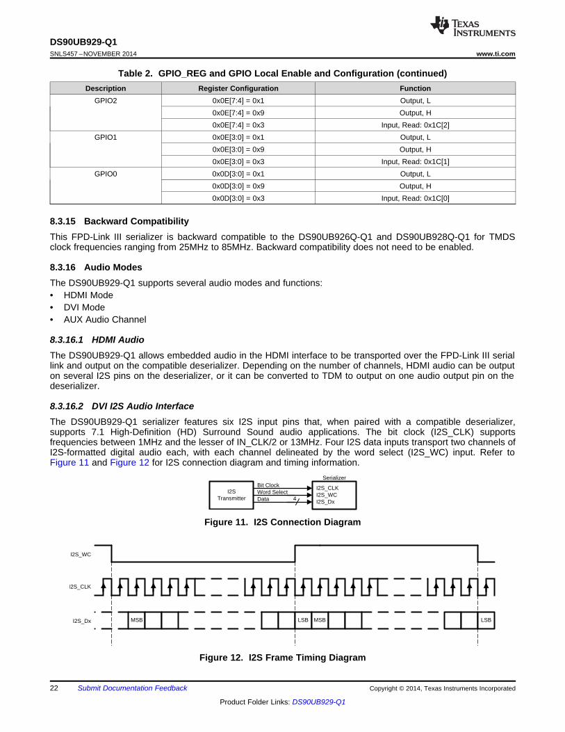
8.3.16.2 DVI I2S Audio InterfaceThe DS90UB929-Q1 serializer features six I2S input pins that, when paired with a compatible deserializer,supports 7.1 High-Definition (HD) Surround Sound audio applications. The bit clock (I2S_CLK) supportsfrequencies between 1MHz and the lesser of IN_CLK/2 or 13MHz. Four I2S data inputs transport two channels ofI2S-formatted digital audio each, with each channel delineated by the word select (I2S_WC) input. Refer toFigure 11 and Figure 12 for I2S connection diagram and timing information.
Figure 11. I2S Connection Diagram
Figure 12. I2S Frame Timing Diagram
22 Submit Documentation Feedback Copyright © 2014, Texas Instruments Incorporated
Product Folder Links: DS90UB929-Q1
DS90UB929-Q1www.ti.com SNLS457 –NOVEMBER 2014
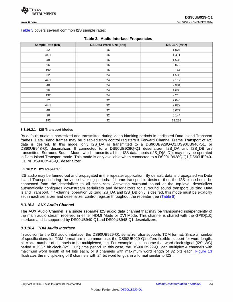
Table 3 covers several common I2S sample rates:
Table 3. Audio Interface FrequenciesSample Rate (kHz) I2S Data Word Size (bits) I2S CLK (MHz)
32 16 1.02444.1 16 1.41148 16 1.53696 16 3.072
192 16 6.14432 24 1.536
44.1 24 2.11748 24 2.30496 24 4.608
192 24 9.21632 32 2.048
44.1 32 2.82248 32 3.07296 32 6.144
192 32 12.288
8.3.16.2.1 I2S Transport Modes
By default, audio is packetized and transmitted during video blanking periods in dedicated Data Island Transportframes. Data Island frames may be disabled from control registers if Forward Channel Frame Transport of I2Sdata is desired. In this mode, only I2S_DA is transmitted to a DS90UB928Q-Q1,DS90UB940-Q1, orDS90UB948-Q1 deserializer. If connected to a DS90UB926Q-Q1 deserializer, I2S_DA and I2S_DB aretransmitted. Surround Sound Mode, which transmits all four I2S data inputs (I2S_D[A..D]), may only be operatedin Data Island Transport mode. This mode is only available when connected to a DS90UB928Q-Q1,DS90UB940-Q1, or DS90UB948-Q1 deserializer.
8.3.16.2.2 I2S Repeater
I2S audio may be fanned-out and propagated in the repeater application. By default, data is propagated via DataIsland Transport during the video blanking periods. If frame transport is desired, then the I2S pins should beconnected from the deserializer to all serializers. Activating surround sound at the top-level deserializerautomatically configures downstream serializers and deserializers for surround sound transport utilizing DataIsland Transport. If 4-channel operation utilizing I2S_DA and I2S_DB only is desired, this mode must be explicitlyset in each serializer and deserializer control register throughout the repeater tree (Table 8).
8.3.16.3 AUX Audio ChannelThe AUX Audio Channel is a single separate I2S audio data channel that may be transported independently ofthe main audio stream received in either HDMI Mode or DVI Mode. This channel is shared with the GPIO[1:0]interface and is supported by DS90UB940-Q1and DS90UB948-Q1 deserializers.
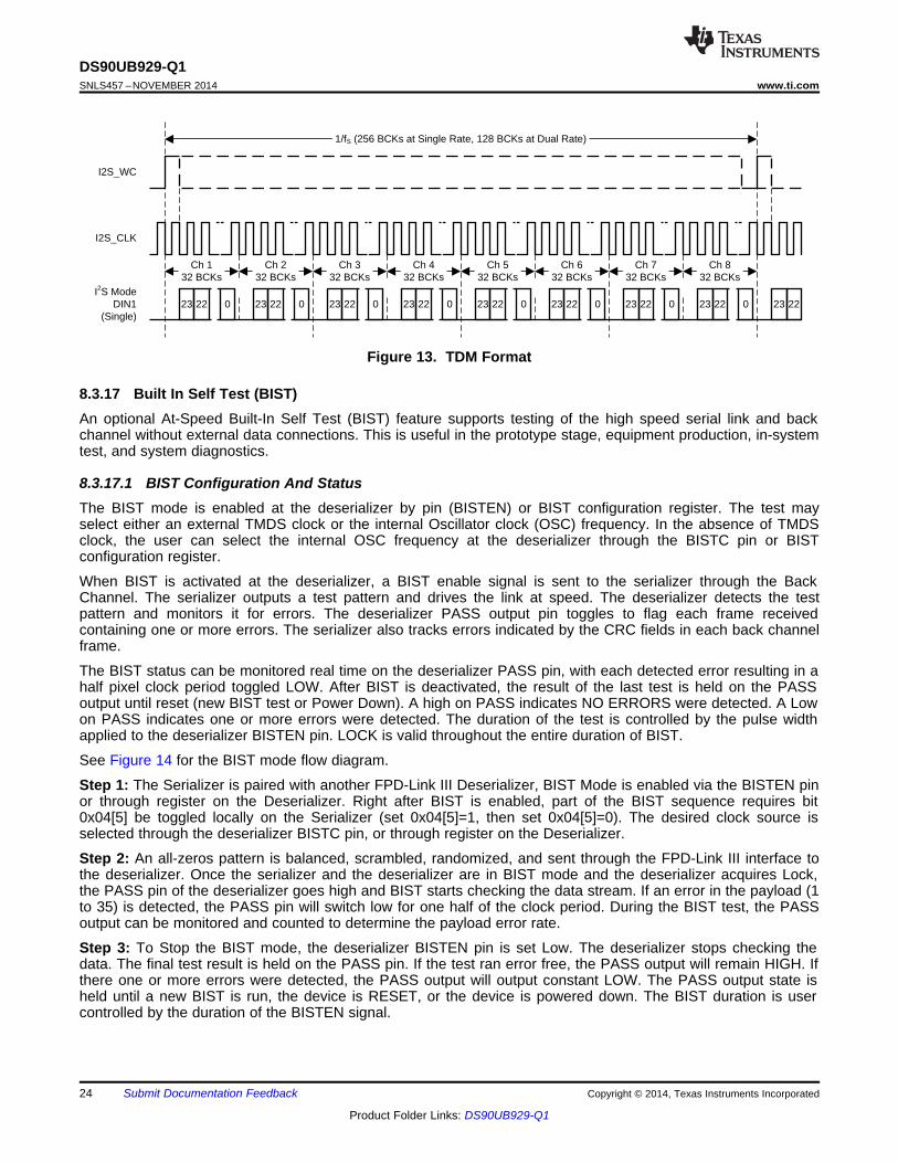
8.3.16.4 TDM Audio InterfaceIn addition to the I2S audio interface, the DS90UB929-Q1 serializer also supports TDM format. Since a numberof specifications for TDM format are in common use, the DS90UB929-Q1 offers flexible support for word length,bit clock, number of channels to be multiplexed, etc. For example, let’s assume that word clock signal (I2S_WC)period = 256 * bit clock (I2S_CLK) time period. In this case, the DS90UB929-Q1 can multiplex 4 channels withmaximum word length of 64 bits each, or 8 channels with maximum word length of 32 bits each. Figure 13illustrates the multiplexing of 8 channels with 24 bit word length, in a format similar to I2S.
Copyright © 2014, Texas Instruments Incorporated Submit Documentation Feedback 23
Product Folder Links: DS90UB929-Q1
I2S_WC
I2S_CLK
I2S Mode DIN1
(Single)
t1/fS (256 BCKs at Single Rate, 128 BCKs at Dual Rate)t
023 22 23 22 0 23 22 0 23 22 0 23 22 0 23 22 0 23 22 0 23 22 0 23 22
Ch 2t32 BCKst
Ch 3t32 BCKst
Ch 4t32 BCKst
Ch 5t32 BCKst
Ch 6t32 BCKst
Ch 7t32 BCKst
Ch 8t32 BCKst
Ch 1t32 BCKst
DS90UB929-Q1SNLS457 –NOVEMBER 2014 www.ti.com
Figure 13. TDM Format
8.3.17 Built In Self Test (BIST)An optional At-Speed Built-In Self Test (BIST) feature supports testing of the high speed serial link and backchannel without external data connections. This is useful in the prototype stage, equipment production, in-systemtest, and system diagnostics.
8.3.17.1 BIST Configuration And StatusThe BIST mode is enabled at the deserializer by pin (BISTEN) or BIST configuration register. The test mayselect either an external TMDS clock or the internal Oscillator clock (OSC) frequency. In the absence of TMDSclock, the user can select the internal OSC frequency at the deserializer through the BISTC pin or BISTconfiguration register.
When BIST is activated at the deserializer, a BIST enable signal is sent to the serializer through the BackChannel. The serializer outputs a test pattern and drives the link at speed. The deserializer detects the testpattern and monitors it for errors. The deserializer PASS output pin toggles to flag each frame receivedcontaining one or more errors. The serializer also tracks errors indicated by the CRC fields in each back channelframe.
The BIST status can be monitored real time on the deserializer PASS pin, with each detected error resulting in ahalf pixel clock period toggled LOW. After BIST is deactivated, the result of the last test is held on the PASSoutput until reset (new BIST test or Power Down). A high on PASS indicates NO ERRORS were detected. A Lowon PASS indicates one or more errors were detected. The duration of the test is controlled by the pulse widthapplied to the deserializer BISTEN pin. LOCK is valid throughout the entire duration of BIST.
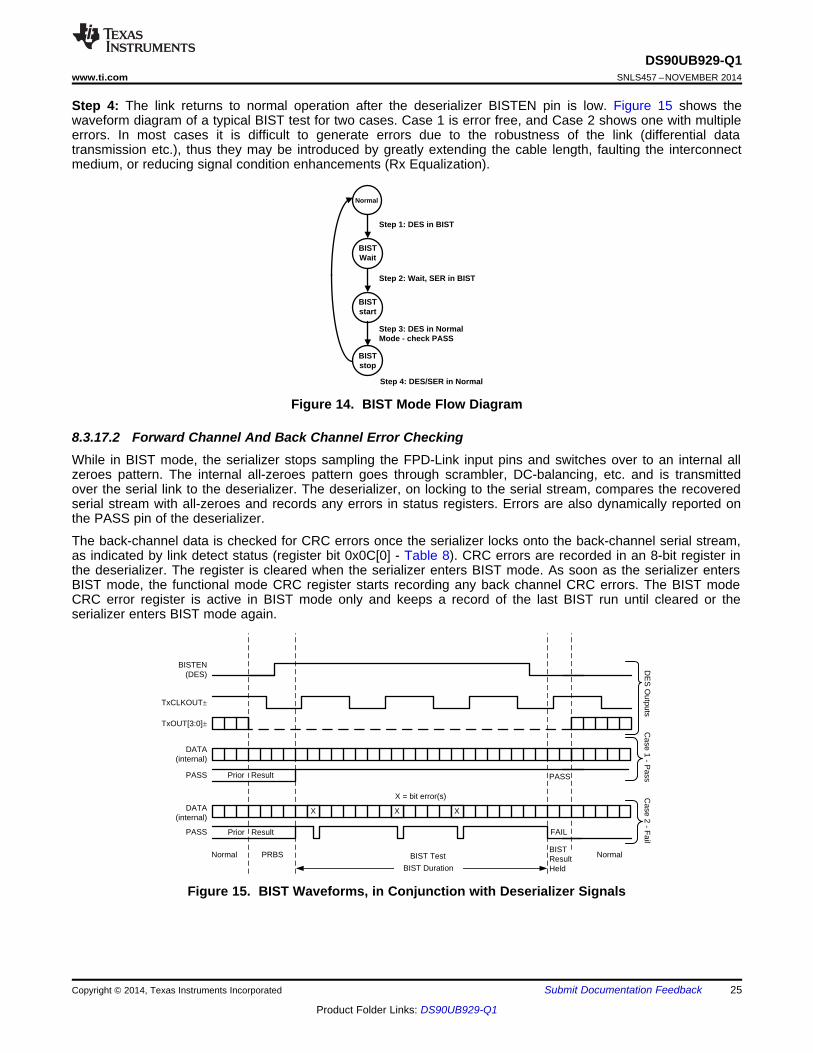
See Figure 14 for the BIST mode flow diagram.
Step 1: The Serializer is paired with another FPD-Link III Deserializer, BIST Mode is enabled via the BISTEN pinor through register on the Deserializer. Right after BIST is enabled, part of the BIST sequence requires bit0x04[5] be toggled locally on the Serializer (set 0x04[5]=1, then set 0x04[5]=0). The desired clock source isselected through the deserializer BISTC pin, or through register on the Deserializer.
Step 2: An all-zeros pattern is balanced, scrambled, randomized, and sent through the FPD-Link III interface tothe deserializer. Once the serializer and the deserializer are in BIST mode and the deserializer acquires Lock,the PASS pin of the deserializer goes high and BIST starts checking the data stream. If an error in the payload (1to 35) is detected, the PASS pin will switch low for one half of the clock period. During the BIST test, the PASSoutput can be monitored and counted to determine the payload error rate.
Step 3: To Stop the BIST mode, the deserializer BISTEN pin is set Low. The deserializer stops checking thedata. The final test result is held on the PASS pin. If the test ran error free, the PASS output will remain HIGH. Ifthere one or more errors were detected, the PASS output will output constant LOW. The PASS output state isheld until a new BIST is run, the device is RESET, or the device is powered down. The BIST duration is usercontrolled by the duration of the BISTEN signal.
24 Submit Documentation Feedback Copyright © 2014, Texas Instruments Incorporated
Product Folder Links: DS90UB929-Q1
X XX
TxCLKOUT±
BISTEN(DES)
PASS
DATA(internal)
PASS
BIST Duration
Prior Result
BIST ResultHeld
PASS
FAIL
X = bit error(s)
TxOUT[3:0]±
DATA(internal)
Case 1 - P
assC
ase 2 - Fail
Prior Result
Normal PRBS BIST Test Normal
DE
S O
utputs
BISTstart
BISTstop
BISTWait
Step 1: DES in BIST
Step 2: Wait, SER in BIST
Step 3: DES in Normal Mode - check PASS
Step 4: DES/SER in Normal
Normal
DS90UB929-Q1www.ti.com SNLS457 –NOVEMBER 2014
Step 4: The link returns to normal operation after the deserializer BISTEN pin is low. Figure 15 shows thewaveform diagram of a typical BIST test for two cases. Case 1 is error free, and Case 2 shows one with multipleerrors. In most cases it is difficult to generate errors due to the robustness of the link (differential datatransmission etc.), thus they may be introduced by greatly extending the cable length, faulting the interconnectmedium, or reducing signal condition enhancements (Rx Equalization).
Figure 14. BIST Mode Flow Diagram
8.3.17.2 Forward Channel And Back Channel Error CheckingWhile in BIST mode, the serializer stops sampling the FPD-Link input pins and switches over to an internal allzeroes pattern. The internal all-zeroes pattern goes through scrambler, DC-balancing, etc. and is transmittedover the serial link to the deserializer. The deserializer, on locking to the serial stream, compares the recoveredserial stream with all-zeroes and records any errors in status registers. Errors are also dynamically reported onthe PASS pin of the deserializer.
The back-channel data is checked for CRC errors once the serializer locks onto the back-channel serial stream,as indicated by link detect status (register bit 0x0C[0] - Table 8). CRC errors are recorded in an 8-bit register inthe deserializer. The register is cleared when the serializer enters BIST mode. As soon as the serializer entersBIST mode, the functional mode CRC register starts recording any back channel CRC errors. The BIST modeCRC error register is active in BIST mode only and keeps a record of the last BIST run until cleared or theserializer enters BIST mode again.
Figure 15. BIST Waveforms, in Conjunction with Deserializer Signals
Copyright © 2014, Texas Instruments Incorporated Submit Documentation Feedback 25
Product Folder Links: DS90UB929-Q1
DS90UB929-Q1SNLS457 –NOVEMBER 2014 www.ti.com
8.3.18 Internal Pattern GenerationThe DS90UB929-Q1 serializer provides an internal pattern generation feature. It allows basic testing anddebugging of an integrated panel. The test patterns are simple and repetitive and allow for a quick visualverification of panel operation. As long as the device is not in power down mode, the test pattern will bedisplayed even if no input is applied. If no clock is received, the test pattern can be configured to use aprogrammed oscillator frequency. For detailed information, refer to Application Note AN-2198.
8.3.18.1 Pattern OptionsThe DS90UB929-Q1 serializer pattern generator is capable of generating 17 default patterns for use in basictesting and debugging of panels. Each can be inverted using register bits (Table 8), shown below:1. White/Black (default/inverted)2. Black/White3. Red/Cyan4. Green/Magenta5. Blue/Yellow6. Horizontally Scaled Black to White/White to Black7. Horizontally Scaled Black to Red/Cyan to White8. Horizontally Scaled Black to Green/Magenta to White9. Horizontally Scaled Black to Blue/Yellow to White10. Vertically Scaled Black to White/White to Black11. Vertically Scaled Black to Red/Cyan to White12. Vertically Scaled Black to Green/Magenta to White13. Vertically Scaled Black to Blue/Yellow to White14. Custom Color (or its inversion) configured in PGRS15. Black-White/White-Black Checkerboard (or custom checkerboard color, configured in PGCTL)16. YCBR/RBCY VCOM pattern, orientation is configurable from PGCTL17. Color Bars (White, Yellow, Cyan, Green, Magenta, Red, Blue, Black) – Note: not included in the auto-
scrolling feature
Additionally, the Pattern Generator incorporates one user-configurable full-screen 24-bit color, which is controlledby the PGRS, PGGS, and PGBS registers. This is pattern #14. One of the pattern options is statically selected inthe PGCTL register when Auto-Scrolling is disabled. The PGTSC and PGTSO1-8 registers control the patternselection and order when Auto-Scrolling is enabled.
8.3.18.2 Color ModesBy default, the Pattern Generator operates in 24-bit color mode, where all bits of the Red, Green, and Blueoutputs are enabled. 18-bit color mode can be activated from the configuration registers (Table 8). In 18-bitmode, the 6 most significant bits (bits 7-2) of the Red, Green, and Blue outputs are enabled; the 2 leastsignificant bits will be 0.
8.3.18.3 Video Timing ModesThe Pattern Generator has two video timing modes – external and internal. In external timing mode, the PatternGenerator detects the video frame timing present on the DE and VS inputs. If Vertical Sync signaling is notpresent on VS, the Pattern Generator determines Vertical Blank by detecting when the number of inactive pixelclocks (DE = 0) exceeds twice the detected active line length. In internal timing mode, the Pattern Generatoruses custom video timing as configured in the control registers. The internal timing generation may also bedriven by an external clock. By default, external timing mode is enabled. Internal timing or Internal timing withExternal Clock are enabled by the control registers (Table 8).
26 Submit Documentation Feedback Copyright © 2014, Texas Instruments Incorporated
Product Folder Links: DS90UB929-Q1

DS90UB929-Q1www.ti.com SNLS457 –NOVEMBER 2014
8.3.18.4 External TimingIn external timing mode, the Pattern Generator passes the incoming DE, HS, and VS signals unmodified to thevideo control outputs after a two pixel clock delay. It extracts the active frame dimensions from the incomingsignals in order to properly scale the brightness patterns. If the incoming video stream does not use the VSsignal, the Pattern Generator determines the Vertical Blank time by detecting a long period of pixel clocks withoutDE asserted.
8.3.18.5 Pattern InversionThe Pattern Generator also incorporates a global inversion control, located in the PGCFG register, which causesthe output pattern to be bitwise-inverted. For example, the full screen Red pattern becomes full-screen cyan, andthe Vertically Scaled Black to Green pattern becomes Vertically Scaled White to Magenta.
8.3.18.6 Auto ScrollingThe Pattern Generator supports an Auto-Scrolling mode, in which the output pattern cycles through a list ofenabled pattern types. A sequence of up to 16 patterns may be defined in the registers. The patterns mayappear in any order in the sequence and may also appear more than once.
8.3.18.7 Additional FeaturesAdditional pattern generator features can be accessed through the Pattern Generator Indirect Register Map. Itconsists of the Pattern Generator Indirect Address (PGIA reg_0x66 — Table 8) and the Pattern GeneratorIndirect Data (PGID reg_0x67 — Table 8). See Application Note AN-2198.
8.3.19 Spread Spectrum Clock ToleranceThe DS90UB929-Q1 (for DVI mode) tolerates a spread spectrum input clock to help reduce EMI. The followingtriangular SSC profile is supported:• Frequency deviation ≤2.5%• Modulation rate ≤ 100kHz
Note: Maximum frequency deviation and maximum modulation rate are not supported simultaneously. Sometypical examples:• Frequency deviation: 2.5%, modulation rate: 50kHz• Frequency deviation: 1.25%, modulation rate: 100kHz
8.4 Device Functional Modes
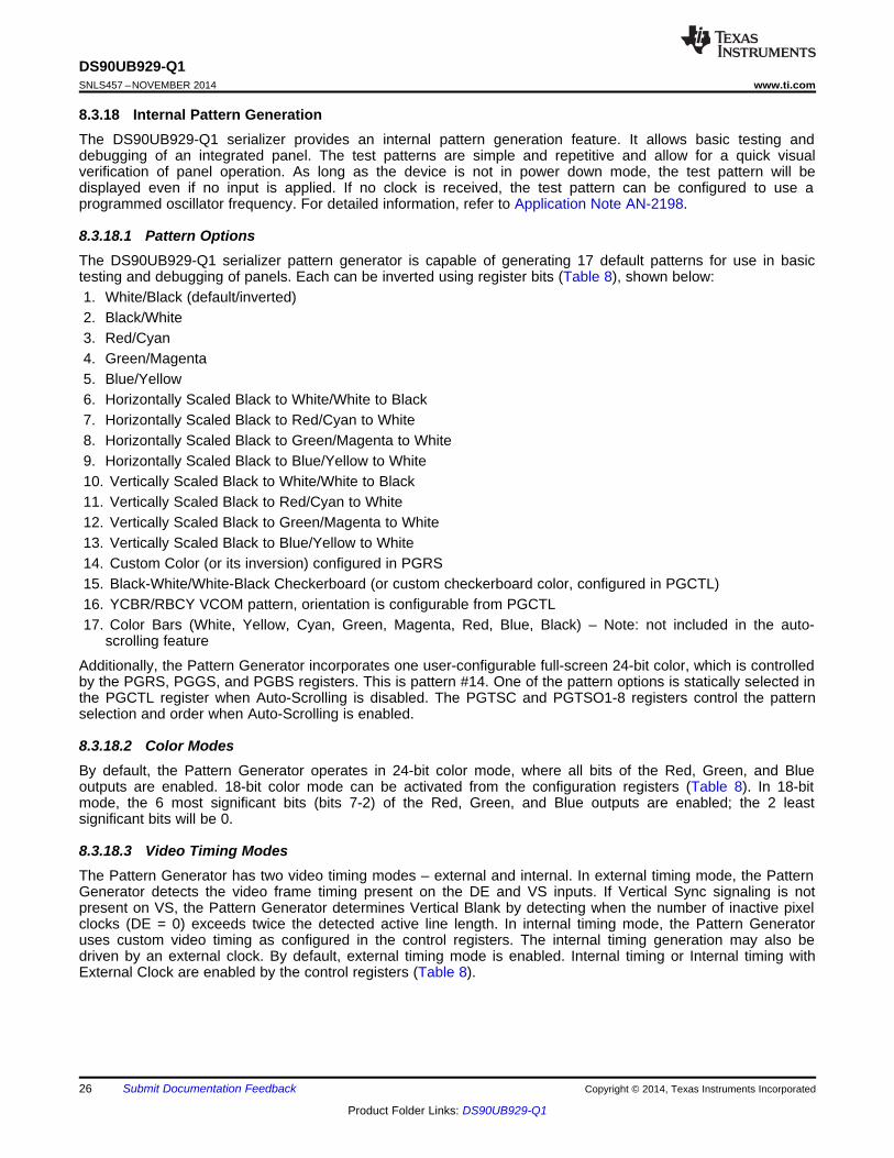
8.4.1 Mode Select Configuration Settings (MODE_SEL[1:0])Configuration of the device may be done via the MODE_SEL[1:0] input pins, or via the configuration register bits.A pull-up resistor and a pull-down resistor of suggested values may be used to set the voltage ratio of theMODE_SEL[1:0] inputs. See Table 5 and Table 6. These values will be latched into register location duringpower-up:
Table 4. MODE_SEL[1:0] SettingsMode Setting Function
Look for remote EDID, if none found, use internal SRAM EDID. Can be overridden0 from register. Remote EDID address may be overridden from default 0xA0.EDID_SEL: Display ID Select1 Use external local EDID.0 Disable.
AUTO-SS: Auto Sleep-State1 Enable.0 HDMI audio.
AUX_I2S: AUX Audio Channel1 HDMI + AUX audio channel.0 Internal HDMI control.EXT_CTL: External Controller
Override 1 External HDMI control from I2C interface pins.
Copyright © 2014, Texas Instruments Incorporated Submit Documentation Feedback 27
Product Folder Links: DS90UB929-Q1
SerializerR4
MODE_SEL0
1.8V
R3
VR4
R6
1.8V
R5
VR6
MODE_SEL1
DS90UB929-Q1SNLS457 –NOVEMBER 2014 www.ti.com
Device Functional Modes (continued)Table 4. MODE_SEL[1:0] Settings (continued)
Mode Setting Function0 Enable FPD-Link III for twisted pair cabling.
COAX: Cable Type1 Enable FPD-Link III for coaxial cabling.0 Use internal SRAM EDID.REM_EDID_LOAD: Remote
EDID Load 1 If available, remote EDID is copied into internal SRAM EDID.
Figure 16. MODE_SEL[1:0] Connection Diagram
Table 5. Configuration Select (MODE_SEL0)# Ratio Target VR4 Suggested Suggested EDID_SEL AUTO_SS AUX_I2S
VR4/VDD18 (V) Resistor Pull-Up Resistor Pull-R3 kΩ (1% tol) Down R4 kΩ (1%
tol)1 0 0 OPEN 40.2 0 0 02 0.208 0.374 118 30.9 0 0 13 0.323 0.582 107 51.1 0 1 04 0.440 0.792 113 88.7 0 1 15 0.553 0.995 82.5 102 1 0 06 0.668 1.202 68.1 137 1 0 17 0.789 1.420 56.2 210 1 1 08 1 1.8 13.3 OPEN 1 1 1
Table 6. Configuration Select (MODE_SEL1)# Ratio Target VR6 Suggested Suggested EXT_CTL COAX REM_EDID_LOA
VR6/VDD18 (V) Resistor Pull-Up Resistor Pull- DR5 kΩ (1% tol) Down R6 kΩ (1%
tol)1 0 0 OPEN 40.2 0 0 02 0.208 0.374 118 30.9 0 0 13 0.323 0.582 107 51.1 0 1 04 0.440 0.792 113 88.7 0 1 15 0.553 0.995 82.5 102 1 0 06 0.668 1.202 68.1 137 1 0 17 0.789 1.420 56.2 210 1 1 08 1 1.8 13.3 OPEN 1 1 1
The strapped values can be viewed and/or modified in the following locations:• EDID_SEL : Latched into BRIDGE_CTL[0], EDID_DISABLE (0x4F[0]).• AUTO_SS : Latched into SOFT_SLEEP (0x01[7]).• AUX_I2S : Latched into BRIDGE_CFG[1], AUDIO_MODE[1] (0x54[1]).• EXT_CTL: Latched into BRIDGE_CFG[7], EXT_CONTROL (0x54[7]).
28 Submit Documentation Feedback Copyright © 2014, Texas Instruments Incorporated
Product Folder Links: DS90UB929-Q1
HOST SER
SCL
SDA
4.7k 4.7k R2
SCL
SDA
To other Devices
IDx
VDD18
R1VDDI2C
VR2
DS90UB929-Q1www.ti.com SNLS457 –NOVEMBER 2014
• COAX : Latched into DUAL_CTL1[7], COAX_MODE (0x5B[7]).• REM_EDID_LOAD : Latched into BRIDGE_CFG[5] (0x54[5]).
8.4.2 FPD-Link III Single Link OperationThe DS90UB929-Q1's single link mode transmits the video over a single FPD-Link III to a single receiver. Singlelink mode supports frequencies up to 96MHz for 24-bit video when paired with the DS90UB940-Q1/DS90UB948-Q1. This mode is compatible with the DS90UB926Q-Q1/DS90UB928Q-Q1 when operating below 85MHz.
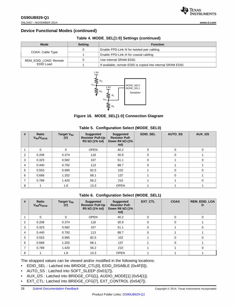
8.5 Programming
8.5.1 Serial Control BusThis serializer may also be configured by the use of a I2C compatible serial control bus. Multiple devices mayshare the serial control bus (up to 8 device addresses supported). The device address is set via a resistor divider(R1 and R2 — see Figure 17 below) connected to the IDx pin.
Figure 17. Serial Control Bus Connection
The serial control bus consists of two signals, SCL and SDA. SCL is a Serial Bus Clock Input. SDA is the SerialBus Data Input / Output signal. Both SCL and SDA signals require an external pull-up resistor to VDD18 or VDD33.For most applications, a 4.7kΩ pull-up resistor is recommended. However, the pull-up resistor value may beadjusted for capacitive loading and data rate requirements. The signals are either pulled High, or driven Low.
The IDx pin configures the control interface to one of 8 possible device addresses. A pull-up resistor and a pull-down resistor may be used to set the appropriate voltage on the IDx input pin See Table 8 below.
Table 7. Serial Control Bus Addresses For IDxRatio Ideal VR2 Suggested Resistor Suggested Resistor# 7-Bit Address 8-Bit AddressVR2 / VDD18 (V) R1 kΩ (1% tol) R2 kΩ (1% tol)
1 0 0 OPEN 40.2 0x0C 0x182 0.208 0.374 118 30.9 0x0E 0x1C3 0.323 0.582 107 51.1 0x10 0x204 0.440 0.792 113 88.7 0x12 0x245 0.553 0.995 82.5 102 0x14 0x286 0.668 1.202 68.1 137 0x16 0x2C7 0.789 1.420 56.2 210 0x18 0x308 1 1.8 13.3 OPEN 0x1A 0x34
Copyright © 2014, Texas Instruments Incorporated Submit Documentation Feedback 29
Product Folder Links: DS90UB929-Q1
Slave Address Register Address Data
S 0ack
ack
ack P
A0
A1
A2
Slave Address Register Address Slave Address Data
S 0 1ack
ack
ack
ackS P
A0
A1
A2
A1
A2
A0
SDA
SCL
S PSTART condition, orSTART repeat condition
STOP condition
DS90UB929-Q1SNLS457 –NOVEMBER 2014 www.ti.com
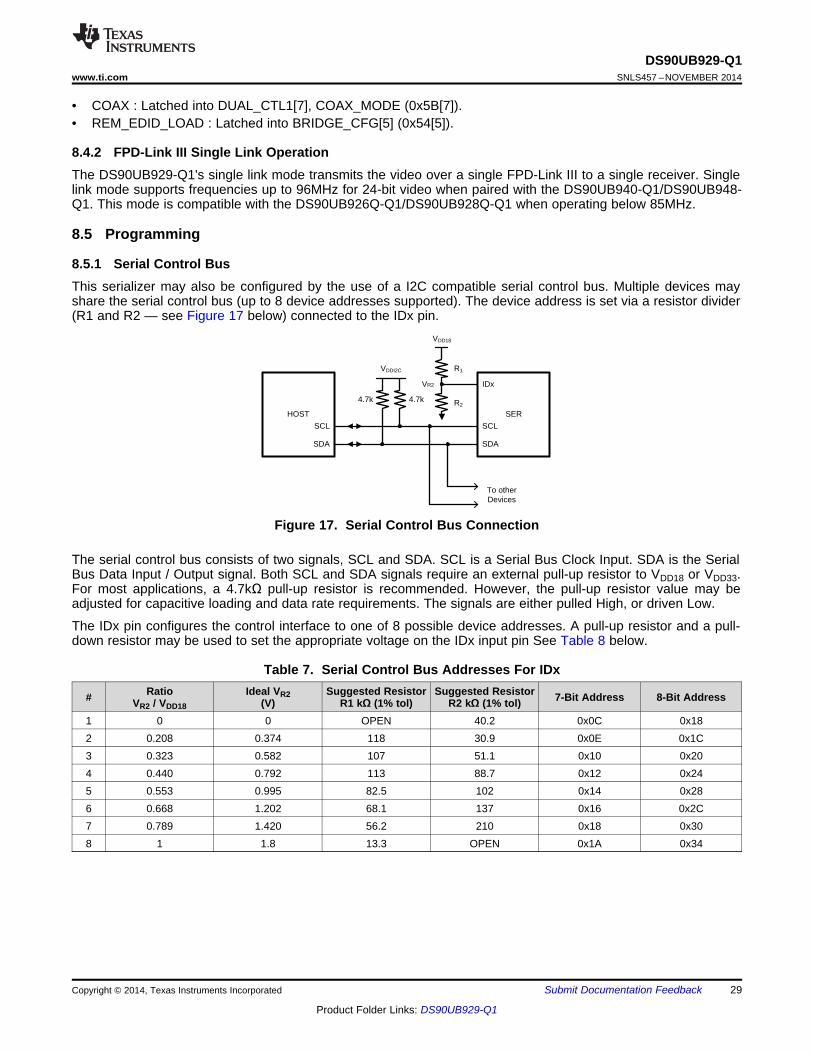
The Serial Bus protocol is controlled by START, START-Repeated, and STOP phases. A START occurs whenSCL transitions Low while SDA is High. A STOP occurs when SDA transitions High while SCL is also HIGH. SeeFigure 18
Figure 18. Start And Stop Conditions
To communicate with an I2C slave, the host controller (master) sends the slave address and listens for aresponse from the slave. This response is referred to as an acknowledge bit (ACK). If a slave on the bus isaddressed correctly, it Acknowledges (ACKs) the master by driving the SDA bus low. If the address doesn'tmatch a device's slave address, it Not-acknowledges (NACKs) the master by letting SDA be pulled High. ACKsalso occur on the bus when data is being transmitted. When the master is writing data, the slave ACKs afterevery data byte is successfully received. When the master is reading data, the master ACKs after every databyte is received to let the slave know it wants to receive another data byte. When the master wants to stopreading, it NACKs after the last data byte and creates a stop condition on the bus. All communication on the busbegins with either a Start condition or a Repeated Start condition. All communication on the bus ends with a Stopcondition. A READ is shown in Figure 25 and a WRITE is shown in Figure 26.
Figure 19. Serial Control Bus — Read
Figure 20. Serial Control Bus — Write
The I2C Master located at the serializer must support I2C clock stretching. For more information on I2C interfacerequirements and throughput considerations, please refer to TI Application Note SNLA131.
8.5.2 Multi-Master Arbitration SupportThe Bidirectional Control Channel in the FPD-Link III devices implements I2C compatible bus arbitration in theproxy I2C master implementation. When sending a data bit, each I2C master senses the value on the SDA line.If the master is sending a logic 1 but senses a logic 0, the master has lost arbitration. It will stop driving SDA,retrying the transaction when the bus becomes idle. Thus, multiple I2C masters may be implemented in thesystem.
If the system does require master-slave operation in both directions across the BCC, some method ofcommunication must be used to ensure only one direction of operation occurs at any time. The communicationmethod could include using available read/write registers in the deserializer to allow masters to communicatewith each other to pass control between the two masters. An example would be to use register 0x18 or 0x19 inthe deserializer as a mailbox register to pass control of the channel from one master to another.
8.5.3 I2C Restrictions on Multi-Master OperationThe I2C specification does not provide for arbitration between masters under certain conditions. The systemshould make sure the following conditions cannot occur to prevent undefined conditions on the I2C bus:• One master generates a repeated Start while another master is sending a data bit.• One master generates a Stop while another master is sending a data bit.
30 Submit Documentation Feedback Copyright © 2014, Texas Instruments Incorporated
Product Folder Links: DS90UB929-Q1

DS90UB929-Q1www.ti.com SNLS457 –NOVEMBER 2014
• One master generates a repeated Start while another master sends a Stop.
Note that these restrictions mainly apply to accessing the same register offsets within a specific I2C slave.
8.5.4 Multi-Master Access to Device Registers for Newer FPD-Link III DevicesWhen using the latest generation of FPD-Link III devices, DS90UB929-Q1 or DS90UB940-Q1/DS90UB948-Q1registers may be accessed simultaneously from both local and remote I2C masters. These devices have internallogic to properly arbitrate between sources to allow proper read and write access without risk of corruption.
Access to remote I2C slaves would still be allowed in only one direction at a time .
8.5.5 Multi-Master Access to Device Registers for Older FPD-Link III DevicesWhen using older FPD-Link III devices, simultaneous access to serializer or deserializer registers from both localand remote I2C masters may cause incorrect operation, thus restrictions should be imposed on accessing ofserializer and deserializer registers. The likelihood of an error occurrence is relatively small, but it is possible forcollision on reads and writes to occur, resulting in an errored read or write.
Two basic options are recommended. The first is to allow device register access only from one controller. Thiswould allow only the Host controller to access the serializer registers (local) and the deserializer registers(remote). A controller at the deserializer would not be allowed to access the deserializer or serializer registers.
The second basic option is to allow local register access only with no access to remote serializer or deserializerregisters. The Host controller would be allowed to access the serializer registers while a controller at thedeserializer could access those register only. Access to remote I2C slaves would still be allowed in onedirection .
In a very limited case, remote and local access could be allowed to the deserializer registers at the same time.Register access is guaranteed to work correctly if both local and remote masters are accessing the samedeserializer register. This allows a simple method of passing control of the Bidirectional Control Channel fromone master to another.
8.5.6 Restrictions on Control Channel Direction for Multi-Master OperationOnly one direction should be active at any time across the Bidirectional Control Channel. If both directions arerequired, some method of transferring control between I2C masters should be implemented.
Copyright © 2014, Texas Instruments Incorporated Submit Documentation Feedback 31
Product Folder Links: DS90UB929-Q1
DS90UB929-Q1SNLS457 –NOVEMBER 2014 www.ti.com
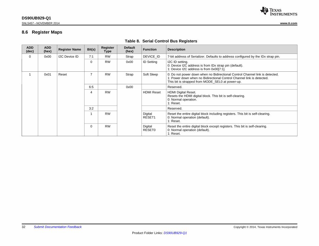
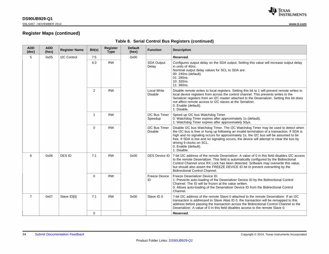
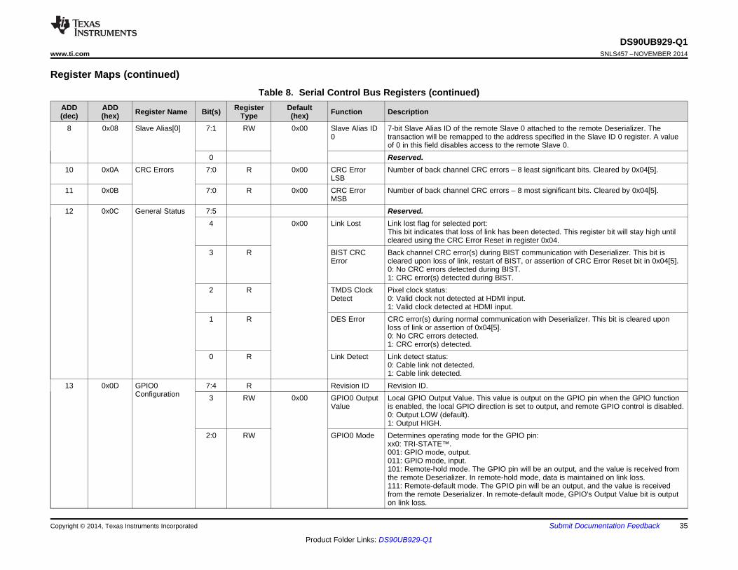
8.6 Register Maps
Table 8. Serial Control Bus RegistersADD ADD Register DefaultRegister Name Bit(s) Function Description(dec) (hex) Type (hex)
0 0x00 I2C Device ID 7:1 RW Strap DEVICE_ID 7-bit address of Serializer. Defaults to address configured by the IDx strap pin.0 RW 0x00 ID Setting I2C ID setting.
0: Device I2C address is from IDx strap pin (default).1: Device I2C address is from 0x00[7:1].
1 0x01 Reset 7 RW Strap Soft Sleep 0: Do not power down when no Bidirectional Control Channel link is detected.1: Power down when no Bidirectional Control Channel link is detected.This bit is strapped from MODE_SEL0 at power-up.
6:5 0x00 Reserved.4 RW HDMI Reset HDMI Digital Reset.
Resets the HDMI digital block. This bit is self-clearing.0: Normal operation.1: Reset.
3:2 Reserved.1 RW Digital Reset the entire digital block including registers. This bit is self-clearing.
RESET1 0: Normal operation (default).1: Reset.
0 RW Digital Reset the entire digital block except registers. This bit is self-clearing.RESET0 0: Normal operation (default).
1: Reset.
32 Submit Documentation Feedback Copyright © 2014, Texas Instruments Incorporated
Product Folder Links: DS90UB929-Q1

DS90UB929-Q1www.ti.com SNLS457 –NOVEMBER 2014
Register Maps (continued)Table 8. Serial Control Bus Registers (continued)
ADD ADD Register DefaultRegister Name Bit(s) Function Description(dec) (hex) Type (hex)3 0x03 General 7 RW 0xD2 Back channel Enable/disable back channel CRC Checker.
Configuration CRC Checker 0: Disable.Enable 1: Enable (default).
6 Reserved.5 RW I2C Remote Automatically acknowledge I2C remote writes. When enabled, I2C writes to the
Write Auto Deserializer (or any remote I2C Slave, if I2C PASS ALL is enabled) are immediatelyAcknowledge acknowledged without waiting for the Deserializer to acknowledge the write. This allows
higher throughput on the I2C bus. Note: this mode will prevent any NACK from a remotedevice from reaching the I2C master.0: Disable (default).1: Enable.
4 RW Filter Enable HS, VS, DE two-clock filter. When enabled, pulses less than two full TMDS clock cycleson the DE, HS, and VS inputs will be rejected.0: Filtering disable.1: Filtering enable (default).
3 RW I2C Pass- I2C pass-through mode. Read/Write transactions matching any entry in the Slave Aliasthrough registers will be passed through to the remote Deserializer.
0: Pass-through disabled (default).1: Pass-through enabled.
2 Reserved.1 RW TMDS Clock Switch over to internal oscillator in the absence of TMDS Clock.
Auto 0: Disable auto-switch.1: Enable auto-switch (default).
0 Reserved.4 0x04 Mode Select 7 RW 0x80 Failsafe State Input failsafe state.
0: Failsafe to High.1: Failsafe to Low (default).
6 Reserved.5 RW CRC Error Clear back channel CRC Error counters. This bit is NOT self-clearing.
Reset 0: Normal operation (default).1: Clear counters.
4:0 Reserved.
Copyright © 2014, Texas Instruments Incorporated Submit Documentation Feedback 33
Product Folder Links: DS90UB929-Q1
DS90UB929-Q1SNLS457 –NOVEMBER 2014 www.ti.com
Register Maps (continued)Table 8. Serial Control Bus Registers (continued)
ADD ADD Register DefaultRegister Name Bit(s) Function Description(dec) (hex) Type (hex)5 0x05 I2C Control 7:5 0x00 Reserved.
4:3 RW SDA Output Configures output delay on the SDA output. Setting this value will increase output delayDelay in units of 40ns.
Nominal output delay values for SCL to SDA are:00: 240ns (default).01: 280ns.10: 320ns.11: 360ns.
2 RW Local Write Disable remote writes to local registers. Setting this bit to 1 will prevent remote writes toDisable local device registers from across the control channel. This prevents writes to the
Serializer registers from an I2C master attached to the Deserializer. Setting this bit doesnot affect remote access to I2C slaves at the Serializer.0: Enable (default).1: Disable.
1 RW I2C Bus Timer Speed up I2C bus Watchdog Timer.Speedup 0: Watchdog Timer expires after approximately 1s (default).
1: Watchdog Timer expires after approximately 50µs.0 RW I2C Bus Timer Disable I2C bus Watchdog Timer. The I2C Watchdog Timer may be used to detect when
Disable the I2C bus is free or hung up following an invalid termination of a transaction. If SDA ishigh and no signaling occurs for approximately 1s, the I2C bus will be assumed to befree. If SDA is low and no signaling occurs, the device will attempt to clear the bus bydriving 9 clocks on SCL.0: Enable (default).1: Disable.
6 0x06 DES ID 7:1 RW 0x00 DES Device ID 7-bit I2C address of the remote Deserializer. A value of 0 in this field disables I2C accessto the remote Deserializer. This field is automatically configured by the BidirectionalControl Channel once RX Lock has been detected. Software may overwrite this value,but should also assert the FREEZE DEVICE ID bit to prevent overwriting by theBidirectional Control Channel.
0 RW Freeze Device Freeze Deserializer Device ID.ID 1: Prevents auto-loading of the Deserializer Device ID by the Bidirectional Control
Channel. The ID will be frozen at the value written.0: Allows auto-loading of the Deserializer Device ID from the Bidirectional ControlChannel.
7 0x07 Slave ID[0] 7:1 RW 0x00 Slave ID 0 7-bit I2C address of the remote Slave 0 attached to the remote Deserializer. If an I2Ctransaction is addressed to Slave Alias ID 0, the transaction will be remapped to thisaddress before passing the transaction across the Bidirectional Control Channel to theDeserializer. A value of 0 in this field disables access to the remote Slave 0.
0 Reserved.
34 Submit Documentation Feedback Copyright © 2014, Texas Instruments Incorporated
Product Folder Links: DS90UB929-Q1
DS90UB929-Q1www.ti.com SNLS457 –NOVEMBER 2014
Register Maps (continued)Table 8. Serial Control Bus Registers (continued)
ADD ADD Register DefaultRegister Name Bit(s) Function Description(dec) (hex) Type (hex)8 0x08 Slave Alias[0] 7:1 RW 0x00 Slave Alias ID 7-bit Slave Alias ID of the remote Slave 0 attached to the remote Deserializer. The
0 transaction will be remapped to the address specified in the Slave ID 0 register. A valueof 0 in this field disables access to the remote Slave 0.
0 Reserved.10 0x0A CRC Errors 7:0 R 0x00 CRC Error Number of back channel CRC errors – 8 least significant bits. Cleared by 0x04[5].
LSB11 0x0B 7:0 R 0x00 CRC Error Number of back channel CRC errors – 8 most significant bits. Cleared by 0x04[5].
MSB12 0x0C General Status 7:5 Reserved.
4 0x00 Link Lost Link lost flag for selected port:This bit indicates that loss of link has been detected. This register bit will stay high untilcleared using the CRC Error Reset in register 0x04.
3 R BIST CRC Back channel CRC error(s) during BIST communication with Deserializer. This bit isError cleared upon loss of link, restart of BIST, or assertion of CRC Error Reset bit in 0x04[5].
0: No CRC errors detected during BIST.1: CRC error(s) detected during BIST.
2 R TMDS Clock Pixel clock status:Detect 0: Valid clock not detected at HDMI input.
1: Valid clock detected at HDMI input.1 R DES Error CRC error(s) during normal communication with Deserializer. This bit is cleared upon
loss of link or assertion of 0x04[5].0: No CRC errors detected.1: CRC error(s) detected.
0 R Link Detect Link detect status:0: Cable link not detected.1: Cable link detected.
13 0x0D GPIO0 7:4 R Revision ID Revision ID.Configuration 3 RW 0x00 GPIO0 Output Local GPIO Output Value. This value is output on the GPIO pin when the GPIO function
Value is enabled, the local GPIO direction is set to output, and remote GPIO control is disabled.0: Output LOW (default).1: Output HIGH.
2:0 RW GPIO0 Mode Determines operating mode for the GPIO pin:xx0: TRI-STATE™.001: GPIO mode, output.011: GPIO mode, input.101: Remote-hold mode. The GPIO pin will be an output, and the value is received fromthe remote Deserializer. In remote-hold mode, data is maintained on link loss.111: Remote-default mode. The GPIO pin will be an output, and the value is receivedfrom the remote Deserializer. In remote-default mode, GPIO's Output Value bit is outputon link loss.
Copyright © 2014, Texas Instruments Incorporated Submit Documentation Feedback 35
Product Folder Links: DS90UB929-Q1

DS90UB929-Q1SNLS457 –NOVEMBER 2014 www.ti.com
Register Maps (continued)Table 8. Serial Control Bus Registers (continued)
ADD ADD Register DefaultRegister Name Bit(s) Function Description(dec) (hex) Type (hex)14 0x0E GPIO1 and 7 RW 0x00 GPIO2 Output Local GPIO Output Value. This value is output on the GPIO pin when the GPIO function
GPIO2 Value is enabled, the local GPIO direction is set to output, and remote GPIO control is disabled.Configuration 0: Output LOW (default).
1: Output HIGH.6:4 RW GPIO2 Mode Determines operating mode for the GPIO pin:
x00: Functional input mode.x10: TRI-STATE™.001: GPIO mode, output.011: GPIO mode, input.101: Remote-hold mode. The GPIO pin will be an output, and the value is received fromthe remote Deserializer. In remote-hold mode, data is maintained on link loss.111: Remote-default mode. The GPIO pin will be an output, and the value is receivedfrom the remote Deserializer. In remote-default mode, GPIO's Output Value bit is outputon link loss.
3 RW GPIO1 Output Local GPIO Output Value. This value is output on the GPIO pin when the GPIO functionValue is enabled, the local GPIO direction is set to output, and remote GPIO control is disabled.
0: Output LOW (default).1: Output HIGH.
2:0 RW GPIO1 Mode Determines operating mode for the GPIO pin:xx0: TRI-STATE™.001: GPIO mode, output.011: GPIO mode, input.101: Remote-hold mode. The GPIO pin will be an output, and the value is received fromthe remote Deserializer. In remote-hold mode, data is maintained on link loss.111: Remote-default mode. The GPIO pin will be an output, and the value is receivedfrom the remote Deserializer. In remote-default mode, GPIO's Output Value bit is outputon link loss.
15 0x0F GPIO3 7:4 0x00 Reserved.Configuration 3 RW GPIO3 Output Local GPIO Output Value. This value is output on the GPIO pin when the GPIO function
Value is enabled, the local GPIO direction is set to output, and remote GPIO control is disabled.0: Output LOW (default).1: Output HIGH.
2:0 RW GPIO3 Mode Determines operating mode for the GPIO pin:x00: Functional input mode.x10: TRI-STATE™.001: GPIO mode, output.011: GPIO mode, input.101: Remote-hold mode. The GPIO pin will be an output, and the value is received fromthe remote Deserializer. In remote-hold mode, data is maintained on link loss.111: Remote-default mode. The GPIO pin will be an output, and the value is receivedfrom the remote Deserializer. In remote-default mode, GPIO's Output Value bit is outputon link loss.
36 Submit Documentation Feedback Copyright © 2014, Texas Instruments Incorporated
Product Folder Links: DS90UB929-Q1

DS90UB929-Q1www.ti.com SNLS457 –NOVEMBER 2014
Register Maps (continued)Table 8. Serial Control Bus Registers (continued)
ADD ADD Register DefaultRegister Name Bit(s) Function Description(dec) (hex) Type (hex)16 0x10 GPIO5_REG 7 RW 0x00 GPIO6_REG Local GPIO Output Value. This value is output on the GPIO pin when the GPIO function
and Output Value is enabled and the local GPIO direction is set to output.GPIO6_REG 0: Output LOW (default).Configuration 1: Output HIGH.
6 Reserved.5:4 RW GPIO6_REG Determines operating mode for the GPIO pin:
Mode 00: Functional input mode.10: TRI-STATE™.01: GPIO mode, output.11: GPIO mode; input.
3 RW GPIO5_REG Local GPIO Output Value. This value is output on the GPIO pin when the GPIO functionOutput Value is enabled and the local GPIO direction is set to output.
0: Output LOW (default).1: Output HIGH.
2 Reserved.1:0 RW GPIO5_REG Determines operating mode for the GPIO pin:
Mode 00: Functional input mode.10: TRI-STATE™.01: GPIO mode, output.11: GPIO mode; input.
17 0x11 GPIO7_REG 7 RW 0x00 GPIO8_REG Local GPIO Output Value. This value is output on the GPIO pin when the GPIO functionand Output Value is enabled and the local GPIO direction is set to output.GPIO8_REG 0: Output LOW (default).Configuration 1: Output HIGH.
6 Reserved.5:4 RW GPIO8_REG Determines operating mode for the GPIO pin:
Mode 00: Functional input mode.10: TRI-STATE.01: GPIO mode, output.11: GPIO mode; input.
3 RW GPIO7_REG Local GPIO Output Value. This value is output on the GPIO pin when the GPIO functionOutput Value is enabled and the local GPIO direction is set to output.
0: Output LOW (default).1: Output HIGH.
2 Reserved.1:0 RW GPIO7_REG Determines operating mode for the GPIO pin:
Mode 00: Functional input mode.10: TRI-STATE.01: GPIO mode, output.11: GPIO mode; input.
Copyright © 2014, Texas Instruments Incorporated Submit Documentation Feedback 37
Product Folder Links: DS90UB929-Q1
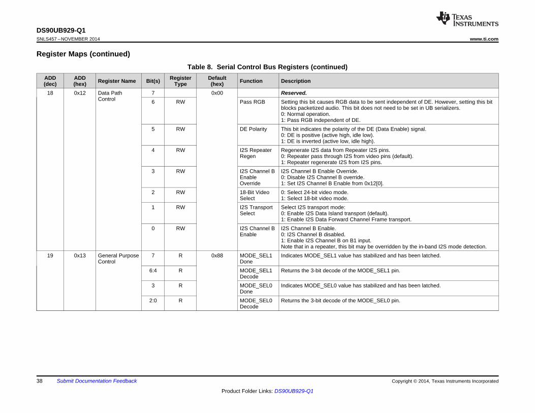
DS90UB929-Q1SNLS457 –NOVEMBER 2014 www.ti.com
Register Maps (continued)Table 8. Serial Control Bus Registers (continued)
ADD ADD Register DefaultRegister Name Bit(s) Function Description(dec) (hex) Type (hex)18 0x12 Data Path 7 0x00 Reserved.
Control 6 RW Pass RGB Setting this bit causes RGB data to be sent independent of DE. However, setting this bitblocks packetized audio. This bit does not need to be set in UB serializers.0: Normal operation.1: Pass RGB independent of DE.
5 RW DE Polarity This bit indicates the polarity of the DE (Data Enable) signal.0: DE is positive (active high, idle low).1: DE is inverted (active low, idle high).
4 RW I2S Repeater Regenerate I2S data from Repeater I2S pins.Regen 0: Repeater pass through I2S from video pins (default).
1: Repeater regenerate I2S from I2S pins.3 RW I2S Channel B I2S Channel B Enable Override.
Enable 0: Disable I2S Channel B override.Override 1: Set I2S Channel B Enable from 0x12[0].
2 RW 18-Bit Video 0: Select 24-bit video mode.Select 1: Select 18-bit video mode.
1 RW I2S Transport Select I2S transport mode:Select 0: Enable I2S Data Island transport (default).
1: Enable I2S Data Forward Channel Frame transport.0 RW I2S Channel B I2S Channel B Enable.
Enable 0: I2S Channel B disabled.1: Enable I2S Channel B on B1 input.Note that in a repeater, this bit may be overridden by the in-band I2S mode detection.
19 0x13 General Purpose 7 R 0x88 MODE_SEL1 Indicates MODE_SEL1 value has stabilized and has been latched.Control Done
6:4 R MODE_SEL1 Returns the 3-bit decode of the MODE_SEL1 pin.Decode
3 R MODE_SEL0 Indicates MODE_SEL0 value has stabilized and has been latched.Done
2:0 R MODE_SEL0 Returns the 3-bit decode of the MODE_SEL0 pin.Decode
38 Submit Documentation Feedback Copyright © 2014, Texas Instruments Incorporated
Product Folder Links: DS90UB929-Q1
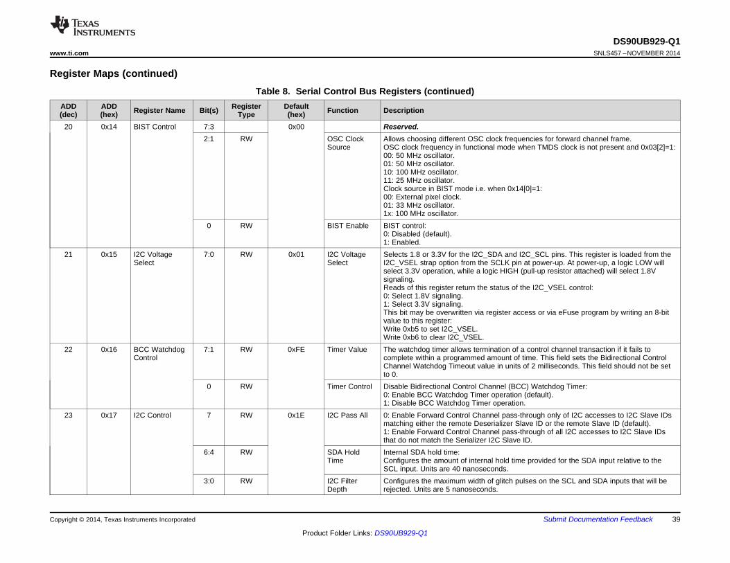
DS90UB929-Q1www.ti.com SNLS457 –NOVEMBER 2014
Register Maps (continued)Table 8. Serial Control Bus Registers (continued)
ADD ADD Register DefaultRegister Name Bit(s) Function Description(dec) (hex) Type (hex)20 0x14 BIST Control 7:3 0x00 Reserved.
2:1 RW OSC Clock Allows choosing different OSC clock frequencies for forward channel frame.Source OSC clock frequency in functional mode when TMDS clock is not present and 0x03[2]=1:
00: 50 MHz oscillator.01: 50 MHz oscillator.10: 100 MHz oscillator.11: 25 MHz oscillator.Clock source in BIST mode i.e. when 0x14[0]=1:00: External pixel clock.01: 33 MHz oscillator.1x: 100 MHz oscillator.
0 RW BIST Enable BIST control:0: Disabled (default).1: Enabled.
21 0x15 I2C Voltage 7:0 RW 0x01 I2C Voltage Selects 1.8 or 3.3V for the I2C_SDA and I2C_SCL pins. This register is loaded from theSelect Select I2C_VSEL strap option from the SCLK pin at power-up. At power-up, a logic LOW will
select 3.3V operation, while a logic HIGH (pull-up resistor attached) will select 1.8Vsignaling.Reads of this register return the status of the I2C_VSEL control:0: Select 1.8V signaling.1: Select 3.3V signaling.This bit may be overwritten via register access or via eFuse program by writing an 8-bitvalue to this register:Write 0xb5 to set I2C_VSEL.Write 0xb6 to clear I2C_VSEL.
22 0x16 BCC Watchdog 7:1 RW 0xFE Timer Value The watchdog timer allows termination of a control channel transaction if it fails toControl complete within a programmed amount of time. This field sets the Bidirectional Control
Channel Watchdog Timeout value in units of 2 milliseconds. This field should not be setto 0.
0 RW Timer Control Disable Bidirectional Control Channel (BCC) Watchdog Timer:0: Enable BCC Watchdog Timer operation (default).1: Disable BCC Watchdog Timer operation.
23 0x17 I2C Control 7 RW 0x1E I2C Pass All 0: Enable Forward Control Channel pass-through only of I2C accesses to I2C Slave IDsmatching either the remote Deserializer Slave ID or the remote Slave ID (default).1: Enable Forward Control Channel pass-through of all I2C accesses to I2C Slave IDsthat do not match the Serializer I2C Slave ID.
6:4 RW SDA Hold Internal SDA hold time:Time Configures the amount of internal hold time provided for the SDA input relative to the
SCL input. Units are 40 nanoseconds.3:0 RW I2C Filter Configures the maximum width of glitch pulses on the SCL and SDA inputs that will be
Depth rejected. Units are 5 nanoseconds.
Copyright © 2014, Texas Instruments Incorporated Submit Documentation Feedback 39
Product Folder Links: DS90UB929-Q1
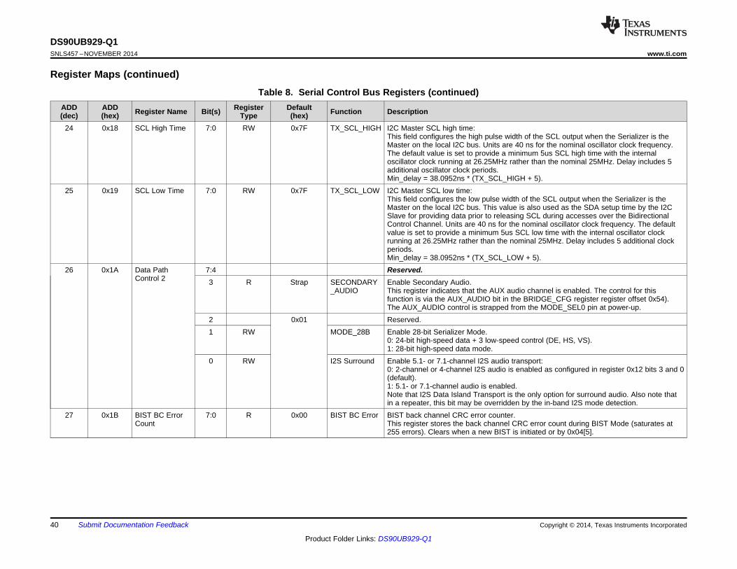
DS90UB929-Q1SNLS457 –NOVEMBER 2014 www.ti.com
Register Maps (continued)Table 8. Serial Control Bus Registers (continued)
ADD ADD Register DefaultRegister Name Bit(s) Function Description(dec) (hex) Type (hex)24 0x18 SCL High Time 7:0 RW 0x7F TX_SCL_HIGH I2C Master SCL high time:
This field configures the high pulse width of the SCL output when the Serializer is theMaster on the local I2C bus. Units are 40 ns for the nominal oscillator clock frequency.The default value is set to provide a minimum 5us SCL high time with the internaloscillator clock running at 26.25MHz rather than the nominal 25MHz. Delay includes 5additional oscillator clock periods.Min_delay = 38.0952ns * (TX_SCL_HIGH + 5).
25 0x19 SCL Low Time 7:0 RW 0x7F TX_SCL_LOW I2C Master SCL low time:This field configures the low pulse width of the SCL output when the Serializer is theMaster on the local I2C bus. This value is also used as the SDA setup time by the I2CSlave for providing data prior to releasing SCL during accesses over the BidirectionalControl Channel. Units are 40 ns for the nominal oscillator clock frequency. The defaultvalue is set to provide a minimum 5us SCL low time with the internal oscillator clockrunning at 26.25MHz rather than the nominal 25MHz. Delay includes 5 additional clockperiods.Min_delay = 38.0952ns * (TX_SCL_LOW + 5).
26 0x1A Data Path 7:4 Reserved.Control 2 3 R Strap SECONDARY Enable Secondary Audio.
_AUDIO This register indicates that the AUX audio channel is enabled. The control for thisfunction is via the AUX_AUDIO bit in the BRIDGE_CFG register register offset 0x54).The AUX_AUDIO control is strapped from the MODE_SEL0 pin at power-up.
2 0x01 Reserved.1 RW MODE_28B Enable 28-bit Serializer Mode.
0: 24-bit high-speed data + 3 low-speed control (DE, HS, VS).1: 28-bit high-speed data mode.
0 RW I2S Surround Enable 5.1- or 7.1-channel I2S audio transport:0: 2-channel or 4-channel I2S audio is enabled as configured in register 0x12 bits 3 and 0(default).1: 5.1- or 7.1-channel audio is enabled.Note that I2S Data Island Transport is the only option for surround audio. Also note thatin a repeater, this bit may be overridden by the in-band I2S mode detection.
27 0x1B BIST BC Error 7:0 R 0x00 BIST BC Error BIST back channel CRC error counter.Count This register stores the back channel CRC error count during BIST Mode (saturates at
255 errors). Clears when a new BIST is initiated or by 0x04[5].
40 Submit Documentation Feedback Copyright © 2014, Texas Instruments Incorporated
Product Folder Links: DS90UB929-Q1
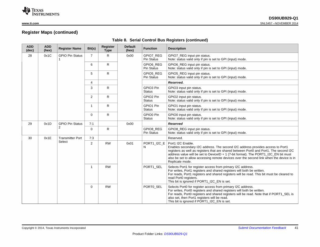
DS90UB929-Q1www.ti.com SNLS457 –NOVEMBER 2014
Register Maps (continued)Table 8. Serial Control Bus Registers (continued)
ADD ADD Register DefaultRegister Name Bit(s) Function Description(dec) (hex) Type (hex)28 0x1C GPIO Pin Status 7 R 0x00 GPIO7_REG GPIO7_REG input pin status.
1 Pin Status Note: status valid only if pin is set to GPI (input) mode.6 R GPIO6_REG GPIO6_REG input pin status.
Pin Status Note: status valid only if pin is set to GPI (input) mode.5 R GPIO5_REG GPIO5_REG input pin status.
Pin Status Note: status valid only if pin is set to GPI (input) mode.4 Reserved.3 R GPIO3 Pin GPIO3 input pin status.
Status Note: status valid only if pin is set to GPI (input) mode.2 R GPIO2 Pin GPIO2 input pin status.
Status Note: status valid only if pin is set to GPI (input) mode.1 R GPIO1 Pin GPIO1 input pin status.
Status Note: status valid only if pin is set to GPI (input) mode.0 R GPIO0 Pin GPIO0 input pin status.
Status Note: status valid only if pin is set to GPI (input) mode.29 0x1D GPIO Pin Status 7:1 0x00 Reserved
2 0 R GPIO8_REG GPIO8_REG input pin status.Pin Status Note: status valid only if pin is set to GPI (input) mode.
30 0x1E Transmitter Port 7:3 Reserved.Select 2 RW 0x01 PORT1_I2C_E Port1 I2C Enable.
N Enables secondary I2C address. The second I2C address provides access to Port1registers as well as registers that are shared between Port0 and Port1. The second I2Caddress value will be set to DeviceID + 1 (7-bit format). The PORT1_I2C_EN bit mustalso be set to allow accessing remote devices over the second link when the device is inReplicate mode.
1 RW PORT1_SEL Selects Port1 for register access from primary I2C address.For writes, Port1 registers and shared registers will both be written.For reads, Port1 registers and shared registers will be read. This bit must be cleared toread Port0 registers.This bit is ignored if PORT1_I2C_EN is set.
0 RW PORT0_SEL Selects Port0 for register access from primary I2C address.For writes, Port0 registers and shared registers will both be written.For reads, Port0 registers and shared registers will be read. Note that if PORT1_SEL isalso set, then Port1 registers will be read.This bit is ignored if PORT1_I2C_EN is set.
Copyright © 2014, Texas Instruments Incorporated Submit Documentation Feedback 41
Product Folder Links: DS90UB929-Q1
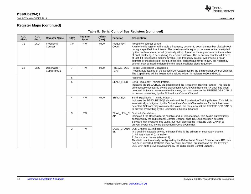
DS90UB929-Q1SNLS457 –NOVEMBER 2014 www.ti.com
Register Maps (continued)Table 8. Serial Control Bus Registers (continued)
ADD ADD Register DefaultRegister Name Bit(s) Function Description(dec) (hex) Type (hex)31 0x1F Frequency 7:0 RW 0x00 Frequency Frequency counter control.
Counter Count A write to this register will enable a frequency counter to count the number of pixel clockduring a specified time interval. The time interval is equal to the value written multipliedby the oscillator clock period (nominally 40ns). A read of the register returns the numberof pixel clock edges seen during the enabled interval. The frequency counter will freezeat 0xff if it reaches the maximum value. The frequency counter will provide a roughestimate of the pixel clock period. If the pixel clock frequency is known, the frequencycounter may be used to determine the actual oscillator clock frequency.
32 0x20 Deserializer 7 RW 0x00 FREEZE_DES Freeze Deserializer Capabilities.Capabilities 1 _CAP Prevent auto-loading of the Deserializer Capabilities by the Bidirectional Control Channel.
The Capabilities will be frozen at the values written in registers 0x20 and 0x21.6 Reserved.5 SEND_FREQ Send Frequency Training Pattern.
Indicates the DS90UB929-Q1 should send the Frequency Training Pattern. This field isautomatically configured by the Bidirectional Control Channel once RX Lock has beendetected. Software may overwrite this value, but must also set the FREEZE DES CAP bitto prevent overwriting by the Bidirectional Control Channel.
4 RW 0x00 SEND_EQ Send Equalization Training Pattern.Indicates the DS90UB929-Q1 should send the Equalization Training Pattern. This field isautomatically configured by the Bidirectional Control Channel once RX Lock has beendetected. Software may overwrite this value, but must also set the FREEZE DES CAP bitto prevent overwriting by the Bidirectional Control Channel.
3 RW DUAL_LINK_C Dual link Capabilities.AP Indicates if the Deserializer is capable of dual link operation. This field is automatically
configured by the Bidirectional Control Channel once RX Lock has been detected.Software may overwrite this value, but must also set the FREEZE DES CAP bit toprevent overwriting by the Bidirectional Control Channel.
2 RW DUAL_CHANN Dual Channel 0/1 Indication.EL In a dual-link capable device, indicates if this is the primary or secondary channel.
0: Primary channel (channel 0).1: Secondary channel (channel 1).This field is automatically configured by the Bidirectional Control Channel once RX Lockhas been detected. Software may overwrite this value, but must also set the FREEZEDES CAP bit to prevent overwriting by the Bidirectional Control Channel.
42 Submit Documentation Feedback Copyright © 2014, Texas Instruments Incorporated
Product Folder Links: DS90UB929-Q1

DS90UB929-Q1www.ti.com SNLS457 –NOVEMBER 2014
Register Maps (continued)Table 8. Serial Control Bus Registers (continued)
ADD ADD Register DefaultRegister Name Bit(s) Function Description(dec) (hex) Type (hex)32 0x20 Deserializer 1 RW 0x00 VID_24B_HD_ Deserializer supports 24-bit video concurrently with HD audio.
Capabilities 1 AUD This field is automatically configured by the Bidirectional Control Channel once RX Lockhas been detected. Software may overwrite this value, but must also set the FREEZEDES CAP bit to prevent overwriting by the Bidirectional Control Channel.
0 RW DES_CAP_FC Deserializer supports GPIO in the Forward Channel Frame._GPIO This field is automatically configured by the Bidirectional Control Channel once RX Lock
has been detected. Software may overwrite this value, but must also set the FREEZEDES CAP bit to prevent overwriting by the Bidirectional Control Channel.
33 0x21 Deserializer 7:2 Reserved.Capabilities 2 1:0 Reserved.
38 0x26 Link Detect 7:3 Reserved.Control 2:0 RW 0x00 LINK DETECT Bidirectional Control Channel Link Detect Timer.
TIMER This field configures the link detection timeout period. If the timer expires without validcommunication over the reverse channel, link detect will be deasserted.000: 162 microseconds.001: 325 microseconds.010: 650 microseconds.011: 1.3 milliseconds.100: 10.25 microseconds.101: 20.5 microseconds.110: 41 microseconds.111: 82 microseconds.
Copyright © 2014, Texas Instruments Incorporated Submit Documentation Feedback 43
Product Folder Links: DS90UB929-Q1

DS90UB929-Q1SNLS457 –NOVEMBER 2014 www.ti.com
Register Maps (continued)Table 8. Serial Control Bus Registers (continued)
ADD ADD Register DefaultRegister Name Bit(s) Function Description(dec) (hex) Type (hex)48 0x30 SCLK_CTRL 7 RW 0x00 SCLK/WS SCLK to Word Select Ratio.
0 : 64.1 : 32.
6:5 RW MCLK/SCLK MCLK to SCLK Select Ratio.00 : 4.01 : 2.10 : 1.11 : 8.
4:3 RW CLEAN Clock Cleaner divider.CLOCK_DIV 00 : FPD_VCO_CLOCK/8.
01 : FPD_VCO_CLOCK/4.10 : FPD_VCO_CLOCK/2.11 : AON_OSC.
2:1 RW CLEAN Mode If non-zero, the SCLK Input or HDMI N/CTS generated Audio Clock is cleaned digitallybefore being used.00 : Off.01 : ratio of 1.10 : ratio of 2.11 : ratio of 4.
0 RW MASTER If set, the SCLK I/O and the WS_IO are used as an output and the Clock GenerationCircuits are enabled, otherwise they are inputs.
49 0x31 AUDIO_CTS0 7:0 RW 0x00 CTS[7:0] If non-zero, the CTS value is used to generate a new clock from the PFD PLLs VCO.50 0x32 AUDIO_CTS1 7:0 RW 0x00 CTS[15:8] If non-zero, the CTS value is used to generate a new clock from the PFD PLLs VCO.51 0x33 AUDIO_CTS2 7:0 RW 0x00 CTS[23:16] If non-zero, the CTS value is used to generate a new clock from the PFD PLLs VCO.52 0x34 AUDIO_N0 7:0 RW 0x00 N[7:0] If non-zero, the CTS value is used to generate a new clock from the PFD PLLs VCO.53 0x35 AUDIO_N1 7:0 RW 0x00 N[15:8] If non-zero, the CTS value is used to generate a new clock from the PFD PLLs VCO.54 0x36 AUDIO_N2_CO 7:4 RW 0x00 COEFF[3:0] Selects the LPF_COEFF in the Clock Cleaner (Feedback is divided by 2^COEFF).
EFF 3:0 RW 0x00 N[19:16] If non-zero, the CTS value is used to generate a new clock from the PFD PLLs VCO.55 0x37 CLK_CLEAN_ST 7:6 Reserved.
S 5:3 R 0x00 IN_FIFO_LVL Clock Cleaner Input FIFO Level.2:0 R 0x00 OUT_FIFO_LV Clock Cleaner Output FIFO Level.
L
44 Submit Documentation Feedback Copyright © 2014, Texas Instruments Incorporated
Product Folder Links: DS90UB929-Q1
DS90UB929-Q1www.ti.com SNLS457 –NOVEMBER 2014
Register Maps (continued)Table 8. Serial Control Bus Registers (continued)
ADD ADD Register DefaultRegister Name Bit(s) Function Description(dec) (hex) Type (hex)72 0x48 APB_CTL 7:5 Reserved.
4:3 RW 0x00 APB_SELECT APB Select: Selects target for register access.00 : HDMI APB interface.01 : EDID SRAM.10 : Configuration Data (read only).11 : Die ID (read only).
2 RW APB_AUTO_I APB Auto Increment: Enables auto-increment mode. Upon completion of an APB read orNC write, the APB address will automatically be incremented by 0x4 for HDMI registers or by
0x1 for others.1 RW APB_READ Start APB Read: Setting this bit to a 1 will begin an APB read. Read data will be available
in the APB_DATAx registers. The APB_ADRx registers should be programmed prior tosetting this bit. This bit will be cleared when the read is complete.
0 RW APB_ENABLE APB Interface Enable: Set to a 1 to enable the APB interface. The APB_SELECT bitsindicate what device is selected.
73 0x49 APB_ADR0 7:0 RW 0x00 APB_ADR0 APB Address byte 0 (LSB).74 0x4A APB_ADR1 7:0 RW 0x00 APB_ADR1 APB Address byte 1 (MSB).75 0x4B APB_DATA0 7:0 RW 0x00 APB_DATA0 Byte 0 (LSB) of the APB Interface Data.76 0x4C APB_DATA1 7:0 RW 0x00 APB_DATA1 Byte 1 of the APB Interface Data.77 0x4D APB_DATA2 7:0 RW 0x00 APB_DATA2 Byte 2 of the APB Interface Data.78 0x4E APB_DATA3 7:0 RW 0x00 APB_DATA3 Byte 3 (MSB) of the APB Interface Data.79 0x4F BRIDGE_CTL 7:5 Reserved.
4 RW 0x00 CEC_CLK_SR CEC Clock Source Select: Selects clock source for generating the 32.768kHz clock forC CEC operations in the HDMI Receive Controller.
0 : Selects internal generated clock.1 : Selects external 25MHz oscillator clock.
3 RW CEC_CLK_EN CEC Clock Enable: Enable CEC clock generation. Enables generation of the 32.768kHzclock for the HDMI Receive controller. This bit should be set prior to enabling CECoperation via the HDMI controller registers.
2 RW EDID_CLEAR Clear EDID SRAM: Set to 1 to enable clearing the EDID SRAM. The EDID_INIT bit mustbe set at the same time for the clear to occur. This bit will be cleared when theinitialization is complete.
1 RW EDID_INIT Initialize EDID SRAM from EEPROM: Causes a reload of the EDID SRAM from the non-volatile EDID EEPROM. This bit will be cleared when the initialization is complete.
0 R Strap EDID_DISABL Disable EDID access via DDC/I2C: Disables access to the EDID SRAM via the HDMIE DDC interface. This value is loaded from the MODE_SEL0 pin at power-up.
Copyright © 2014, Texas Instruments Incorporated Submit Documentation Feedback 45
Product Folder Links: DS90UB929-Q1
DS90UB929-Q1SNLS457 –NOVEMBER 2014 www.ti.com
Register Maps (continued)Table 8. Serial Control Bus Registers (continued)
ADD ADD Register DefaultRegister Name Bit(s) Function Description(dec) (hex) Type (hex)80 0x50 BRIDGE_STS 7 R 0x03 RX5V_DETEC RX +5V detect: Indicates status of the RX_5V pin. When asserted, indicates the HDMI
T interface has detected valid voltage on the RX_5V input.6 R HDMI_INT HDMI Interrupt Status: Indicates an HDMI Interrupt is pending. HDMI interrupts are
serviced through the HDMI Registers via the APB Interface.5 Reserved.4 R INIT_DONE Initialization Done: Initialization sequence has completed. This step will complete after
configuration complete (CFG_DONE).3 R REM_EDID_L Remote EDID Loaded: Indicates EDID SRAM has been loaded from a remote EDID
OAD EEPROM device over the Bidirectional Control Channel. The EDID_CKSUM valueindicates if the EDID load was successful.
2 R CFG_DONE Configuration Complete: Indicates automatic configuration has completed. This step willcomplete prior to initialization complete (INIT_DONE).
1 R CFG_CKSUM Configuration checksum status: Indicates result of Configuration checksum duringinitialization. The device verifies the 2’s complement checksum in the last 128 bytes ofthe EEPROM. A value of 1 indicates the checksum passed.
0 R EDID_CKSUM EDID checksum Status: Indicates result of EDID checksum during EDID initialization. Thedevice verifies the 2’s complement checksum in the first 256 bytes of the EEPROM. Avalue of 1 indicates the checksum passed.
81 0x51 EDID_ID 7:1 RW 0x50 EDID_ID EDID I2C Slave Address: I2C address used for accessing the EDID information. Theseare the upper 7 bits in 8-bit format addressing, where the lowest bit is the Read/Writecontrol.
0 RW 0 EDID_RDONL EDID Read Only: Set to a 1 puts the EDID SRAM memory in read-only mode for accessY via the HDMI DDC interface. Setting to a 0 allows writes to the EDID SRAM memory.
82 0x52 EDID_CFG0 7 Reserved.6:4 RW 0x01 EDID_SDA_H Internal SDA Hold Time: This field configures the amount of internal hold time provided
OLD for the DDC_SDA input relative to the DDC_SCL input. Units are 40 nanoseconds. Thehold time is used to qualify the start detection to avoid false detection of Start or Stopconditions.
3:0 RW 0x0E EDID_FLTR_D I2C Glitch Filter Depth: This field configures the maximum width of glitch pulses on thePTH DDC_SCL and DDC_SDA inputs that will be rejected. Units are 5 nanoseconds.
83 0x53 EDID_CFG1 7:2 Reserved.1:0 RW 0x00 EDID_SDA_DL SDA Output Delay: This field configures output delay on the DDC_SDA output when the
Y EDID memory is accessed. Setting this value will increase output delay in units of 40ns.Nominal output delay values for DDC_SCL to DDC_SDA are:00 : 240ns.01 : 280ns.10 : 320ns.11 : 360ns.
46 Submit Documentation Feedback Copyright © 2014, Texas Instruments Incorporated
Product Folder Links: DS90UB929-Q1
DS90UB929-Q1www.ti.com SNLS457 –NOVEMBER 2014
Register Maps (continued)Table 8. Serial Control Bus Registers (continued)
ADD ADD Register DefaultRegister Name Bit(s) Function Description(dec) (hex) Type (hex)84 0x54 BRIDGE_CFG 7 RW Strap EXT_CTL External Control: When this bit Is set, the internal bridge control function is disabled. This
disables initialization of the HDMI Receiver. These operations must be controlled by anexternal controller attached to the I2C interface. This value is loaded from theMODE_SEL1 pin at power-up.
6 RW 0x00 HDMI_INT_EN HDMI Interrupt Enable: When this bit is set, Interrupts from the HDMI Receive controllerwill be reported on the INTB pin. Software may check the BRIDGE_STS register todetermine if the interrupt is from the HDMI Receiver.
5 RW Strap DIS_REM_EDI Disable Remote EDID load: Disables automatic load of EDID SRAM from a remote EDIDD EEPROM. By default, the device will check the remote I2C bus for an EEPROM with a
valid EDID, and load the EDID data to local EDID SRAM. If this bit is set to a 1, theremote EDID load will be bypassed. This value is loaded from the MODE_SEL1 pin atpower-up.
4 RW 0x00 AUTO_INIT_DI Disable Automatic initialization: The Bridge control will automatically initialize the HDMIS Receiver for operation. Setting this bit to a 1 will disable automatic initialization of the
HDMI Receiver. In this mode, initialization of the HDMI Receiver must be done throughEEPROM configuration or via external control.
3 Reserved.2 RW 0x00 AUDIO_TDM Enable TDM Audio: Setting this bit to a 1 will enable TDM audio for the HDMI audio.1 RW AUDIO_MODE Audio Mode: Selects source for audio to be sent over the FPD-Link III downstream link.
0 : HDMI audio.1 : Local/DVI audio.Local audio is sourced from the device I2S pins rather than from HDMI, and is useful inmodes such as DVI that do not include audio.
0 RW Strap AUX_AUDIO_ AUX Audio Channel Enable: Setting this bit to a 1 will enable the AUX audio channel.EN This allows sending additional 2-channel audio in addition to the HDMI or DVI audio. This
bit is loaded from the MODE_SEL0 pin at power-up.
Copyright © 2014, Texas Instruments Incorporated Submit Documentation Feedback 47
Product Folder Links: DS90UB929-Q1

DS90UB929-Q1SNLS457 –NOVEMBER 2014 www.ti.com
Register Maps (continued)Table 8. Serial Control Bus Registers (continued)
ADD ADD Register DefaultRegister Name Bit(s) Function Description(dec) (hex) Type (hex)85 0x55 AUDIO_CFG 7 RW 0x00 TDM_2_PARA Enable I2S TDM to parallel audio conversion: When this bit is set, the i2s tdm to parallel
LLEL conversion module is enabled. The clock output from the i2s tdm to parallel conversionmodule is them used to send data to the deserializer.
6 RW HDMI_I2S_OU HDMI Audio Output Enable: When this bit is set, the HDMI I2S audio data will be outputT on the I2S audio interface pins. This control is ignored if the
BRIDGE_CFG:AUDIO_MODE is not set to 00 (HDMI audio only).5:4 Reserved.3 RW 0x0C RST_ON_TYP Reset Audio FIFO on Type Change: When this bit is set, the internal bridge control
E function will reset the HDMI Audio FIFO on a change in the Audio type.2 RW RST_ON_AIF Reset Audio FIFO on Audio Infoframe: When this bit is set, the internal bridge control
function will reset the HDMI Audio FIFO on a change in the Audio Infoframe checksum.1 RW RST_ON_AVI Reset Audio FIFO on Audio Video Information Infoframe: When this bit is set, the internal
bridge control function will reset the HDMI Audio FIFO on a change in the Audio VideoInformation Infoframe checksum.
0 RW RST_ON_ACR Reset Audio FIFO on Audio Control Frame: When this bit is set, the internal bridgecontrol function will reset the HDMI Audio FIFO on a change in the Audio Control FrameN or CTS fields.
90 0x5A FPD3_STS 7 R 0x00 FPD3_LINK_R This bit indicates that the FPD-Link III has detected a valid downstream connection andDY determined capabilities for the downstream link.
6 R FPD3_TX_ST FPD-Link III transmit status:S This bit indicates that the FPD-Link III transmitter is active and the receiver is LOCKED to
the transmit clock. It is only asserted once a valid input has been detected, and the FPD-Link III transmit connection has entered the correct mode (Single vs. Dual mode).
5:4 R FPD3_PORT_ FPD3 Port Status: If FPD3_TX_STS is set to a 1, this field indicates the port mode statusSTS as follows:
01: Single FPD-Link III Transmit on port 0.3 R TMDS_VALID HDMI TMDS Valid: This bit indicates the TMDS interface is recovering valid TMDS data
from HDMI. In revA1 silicon, this bit will always return 1.2 R HDMI_PLL_LO HDMI PLL lock status: Indicates the HDMI PLL has locked to the incoming HDMI clock.
CK1 R NO_HDMI_CL No HDMI Clock Detected: This bit indicates the Frequency Detect circuit did not detect an
K HDMI clock greater than the value specified in the FREQ_LOW register.0 R FREQ_STABL HDMI Frequency is Stable: Indicates the Frequency Detection circuit has detected a
E stable HDMI clock frequency.
48 Submit Documentation Feedback Copyright © 2014, Texas Instruments Incorporated
Product Folder Links: DS90UB929-Q1
DS90UB929-Q1www.ti.com SNLS457 –NOVEMBER 2014
Register Maps (continued)Table 8. Serial Control Bus Registers (continued)
ADD ADD Register DefaultRegister Name Bit(s) Function Description(dec) (hex) Type (hex)91 0x5B FPD3_CTL1 7 RW Strap FPD3_COAX_ FPD3 Coax Mode: Enables configuration for the FPD3 Interface cabling type.
MODE 0 : Twisted Pair.1 : Coax This bit is loaded from the MODE_SEL1 pin at power-up.
6 Reserved.5 RW 1 RST_PLL_FR Reset FPD3 PLL on Frequency Change: When set to a 1, frequency changes detected
EQ by the Frequency Detect circuit will result in a reset of the FPD3 PLL.4 RW 0 FREQ_DET_P Frequency Detect Select PLL Clock: Determines the clock source for the Frequency
LL detection circuit:0 : HDMI clock (prior to PLL).1: HDMI PLL clock.
3 Reserved.2 Reserved.1 Reserved.0 Reserved.
92 0x5C FPD3_CTL2 7 Reserved.6 RW 0x00 FORCE_LINK_ Force Link Ready: Forces link ready indication, bypassing back channel link detection.
RDY5 RW FORCE_CLK_ Force Clock Detect: Forces the HDMI/OpenLDI clock detect circuit to indicate presence
DET of a valid input clock. This bypasses the clock detect circuit, allowing operation with aninput clock that does not meet frequency or stability requirements.
4:3 RW FREQ_STBL_ Frequency Stability Threshold: The Frequency detect circuit can be used to detect aTHR stable clock frequency. The Stability Threshold determines the amount of time required
for the clock frequency to stay within the FREQ_HYST range to be considered stable:00 : 160us.01 : 640us.10 : 1.28ms.11 : 2.55ms.
2:0 RW 0x02 FREQ_HYST Frequency Detect Hysteresis: The Frequency detect hysteresis setting allows ignoringminor fluctuations in frequency. A new frequency measurement will be captured only ifthe measured frequency differs from the current measured frequency by more than theFREQ_HYST setting. The FREQ_HYST setting is in MHz.
93 0x5D FREQ_LOW 7 Reserved.6 RW 0 HDMI_RST_M HDMI Phy Reset Mode:
ODE 0 : Reset HDMI Phy on change in mode or frequency.1 : Don't reset HDMI Phy on change in mode or frequency if +5V is asserted.
5:0 RW 6 FREQ_LO_TH Frequency Low Threshold: Sets the low threshold for the HDMI Clock frequency detectR circuit in MHz. This value is used to determine if the HDMI clock frequency is too low for
proper operation.
Copyright © 2014, Texas Instruments Incorporated Submit Documentation Feedback 49
Product Folder Links: DS90UB929-Q1
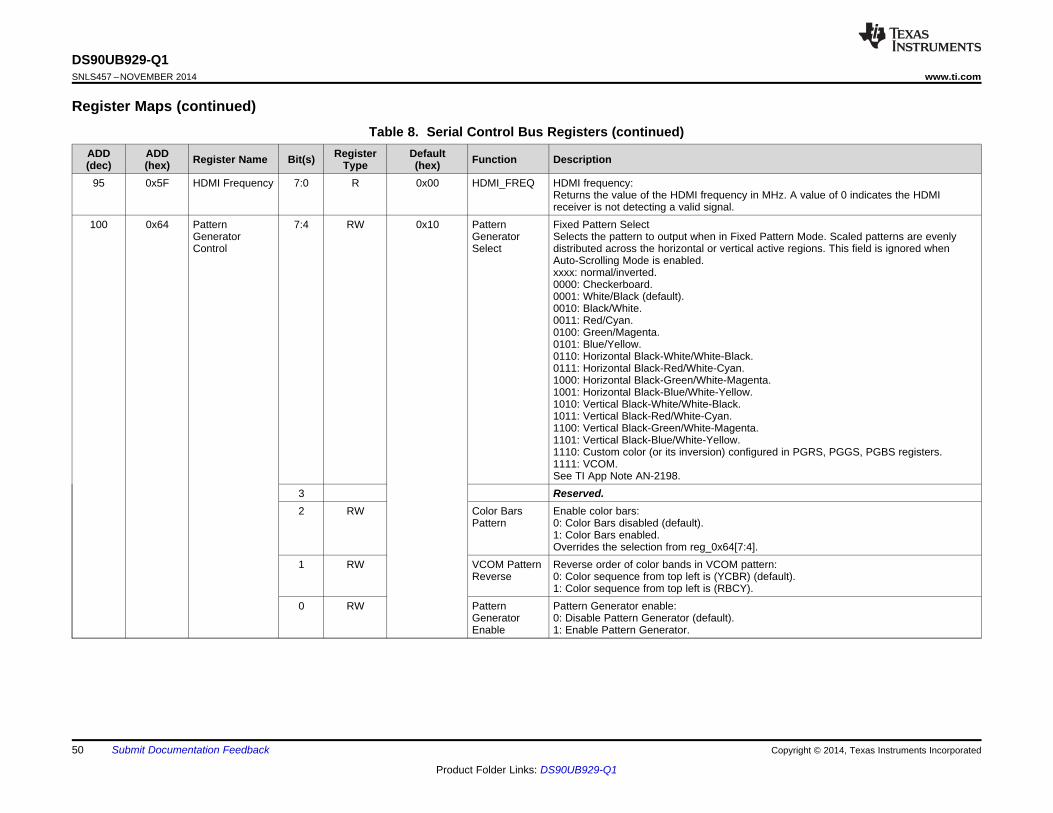
DS90UB929-Q1SNLS457 –NOVEMBER 2014 www.ti.com
Register Maps (continued)Table 8. Serial Control Bus Registers (continued)
ADD ADD Register DefaultRegister Name Bit(s) Function Description(dec) (hex) Type (hex)95 0x5F HDMI Frequency 7:0 R 0x00 HDMI_FREQ HDMI frequency:
Returns the value of the HDMI frequency in MHz. A value of 0 indicates the HDMIreceiver is not detecting a valid signal.
100 0x64 Pattern 7:4 RW 0x10 Pattern Fixed Pattern SelectGenerator Generator Selects the pattern to output when in Fixed Pattern Mode. Scaled patterns are evenlyControl Select distributed across the horizontal or vertical active regions. This field is ignored when
Auto-Scrolling Mode is enabled.xxxx: normal/inverted.0000: Checkerboard.0001: White/Black (default).0010: Black/White.0011: Red/Cyan.0100: Green/Magenta.0101: Blue/Yellow.0110: Horizontal Black-White/White-Black.0111: Horizontal Black-Red/White-Cyan.1000: Horizontal Black-Green/White-Magenta.1001: Horizontal Black-Blue/White-Yellow.1010: Vertical Black-White/White-Black.1011: Vertical Black-Red/White-Cyan.1100: Vertical Black-Green/White-Magenta.1101: Vertical Black-Blue/White-Yellow.1110: Custom color (or its inversion) configured in PGRS, PGGS, PGBS registers.1111: VCOM.See TI App Note AN-2198.
3 Reserved.2 RW Color Bars Enable color bars:
Pattern 0: Color Bars disabled (default).1: Color Bars enabled.Overrides the selection from reg_0x64[7:4].
1 RW VCOM Pattern Reverse order of color bands in VCOM pattern:Reverse 0: Color sequence from top left is (YCBR) (default).
1: Color sequence from top left is (RBCY).0 RW Pattern Pattern Generator enable:
Generator 0: Disable Pattern Generator (default).Enable 1: Enable Pattern Generator.
50 Submit Documentation Feedback Copyright © 2014, Texas Instruments Incorporated
Product Folder Links: DS90UB929-Q1
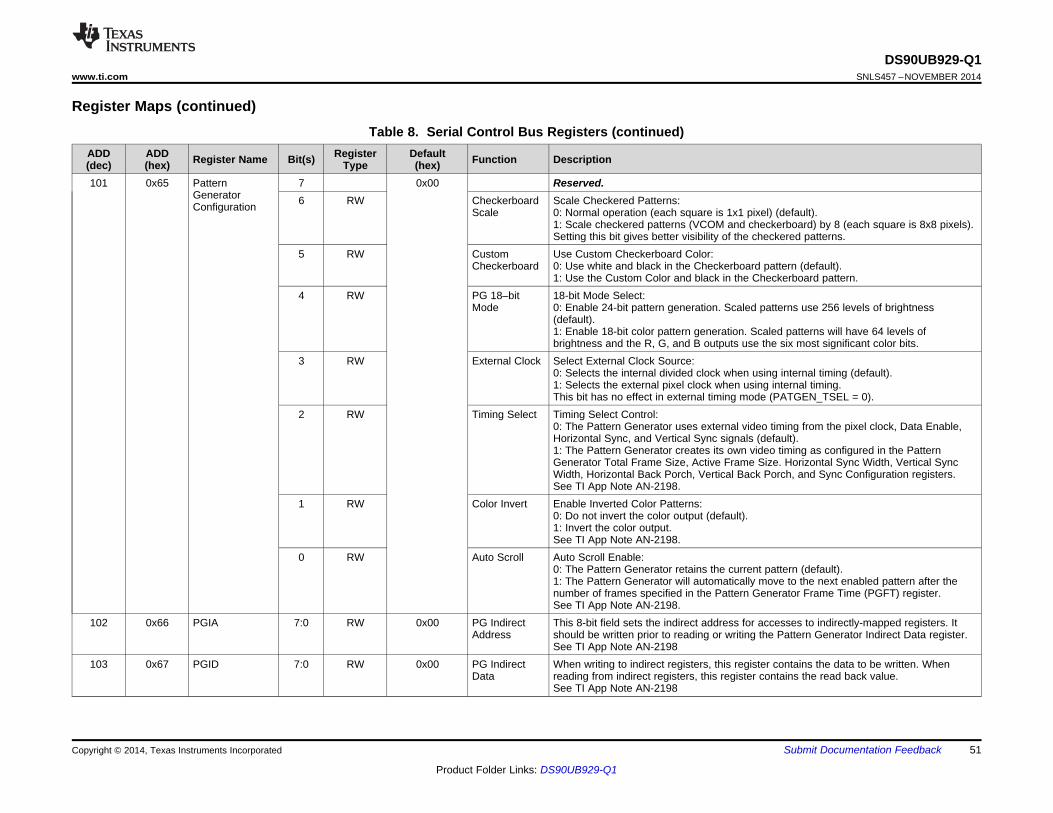
DS90UB929-Q1www.ti.com SNLS457 –NOVEMBER 2014
Register Maps (continued)Table 8. Serial Control Bus Registers (continued)
ADD ADD Register DefaultRegister Name Bit(s) Function Description(dec) (hex) Type (hex)101 0x65 Pattern 7 0x00 Reserved.
Generator 6 RW Checkerboard Scale Checkered Patterns:Configuration Scale 0: Normal operation (each square is 1x1 pixel) (default).1: Scale checkered patterns (VCOM and checkerboard) by 8 (each square is 8x8 pixels).Setting this bit gives better visibility of the checkered patterns.
5 RW Custom Use Custom Checkerboard Color:Checkerboard 0: Use white and black in the Checkerboard pattern (default).
1: Use the Custom Color and black in the Checkerboard pattern.4 RW PG 18–bit 18-bit Mode Select:
Mode 0: Enable 24-bit pattern generation. Scaled patterns use 256 levels of brightness(default).1: Enable 18-bit color pattern generation. Scaled patterns will have 64 levels ofbrightness and the R, G, and B outputs use the six most significant color bits.
3 RW External Clock Select External Clock Source:0: Selects the internal divided clock when using internal timing (default).1: Selects the external pixel clock when using internal timing.This bit has no effect in external timing mode (PATGEN_TSEL = 0).
2 RW Timing Select Timing Select Control:0: The Pattern Generator uses external video timing from the pixel clock, Data Enable,Horizontal Sync, and Vertical Sync signals (default).1: The Pattern Generator creates its own video timing as configured in the PatternGenerator Total Frame Size, Active Frame Size. Horizontal Sync Width, Vertical SyncWidth, Horizontal Back Porch, Vertical Back Porch, and Sync Configuration registers.See TI App Note AN-2198.
1 RW Color Invert Enable Inverted Color Patterns:0: Do not invert the color output (default).1: Invert the color output.See TI App Note AN-2198.
0 RW Auto Scroll Auto Scroll Enable:0: The Pattern Generator retains the current pattern (default).1: The Pattern Generator will automatically move to the next enabled pattern after thenumber of frames specified in the Pattern Generator Frame Time (PGFT) register.See TI App Note AN-2198.
102 0x66 PGIA 7:0 RW 0x00 PG Indirect This 8-bit field sets the indirect address for accesses to indirectly-mapped registers. ItAddress should be written prior to reading or writing the Pattern Generator Indirect Data register.
See TI App Note AN-2198103 0x67 PGID 7:0 RW 0x00 PG Indirect When writing to indirect registers, this register contains the data to be written. When
Data reading from indirect registers, this register contains the read back value.See TI App Note AN-2198
Copyright © 2014, Texas Instruments Incorporated Submit Documentation Feedback 51
Product Folder Links: DS90UB929-Q1
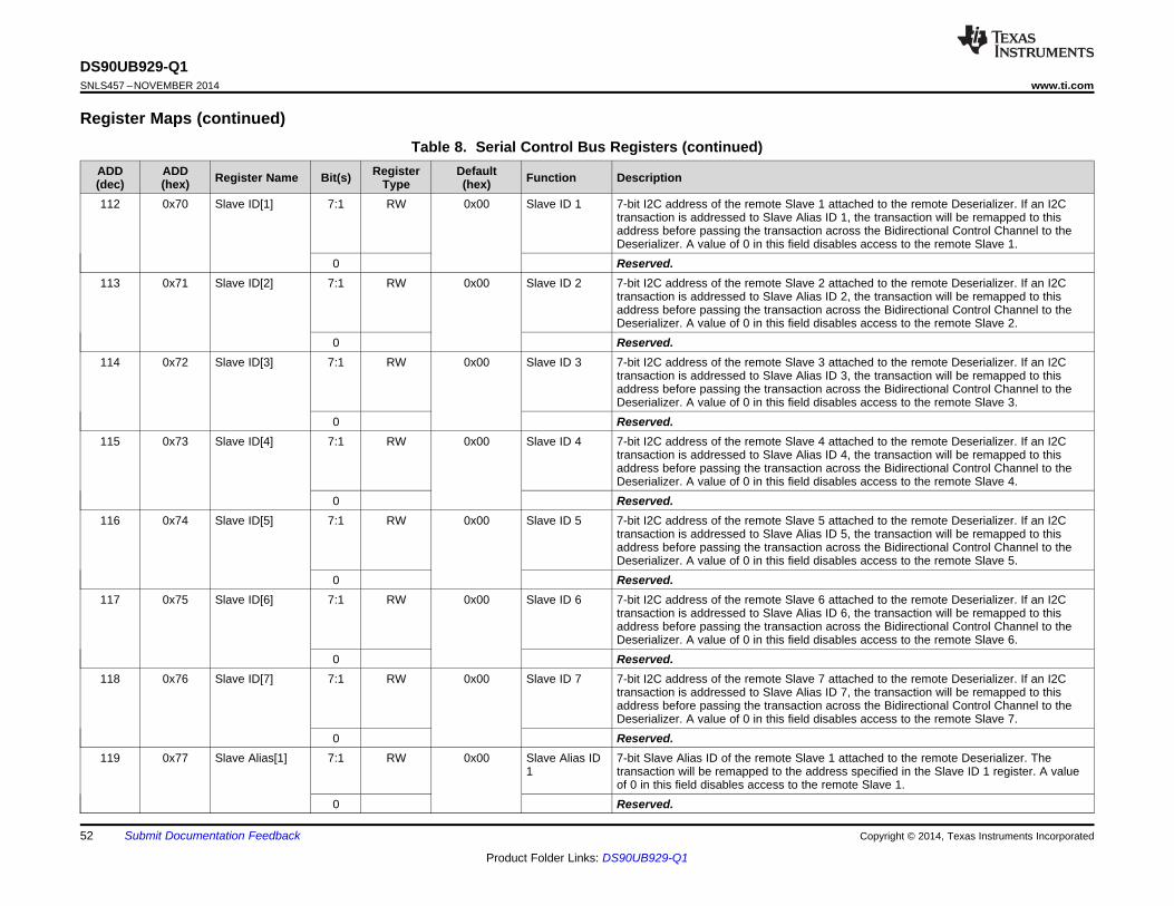
DS90UB929-Q1SNLS457 –NOVEMBER 2014 www.ti.com
Register Maps (continued)Table 8. Serial Control Bus Registers (continued)
ADD ADD Register DefaultRegister Name Bit(s) Function Description(dec) (hex) Type (hex)112 0x70 Slave ID[1] 7:1 RW 0x00 Slave ID 1 7-bit I2C address of the remote Slave 1 attached to the remote Deserializer. If an I2C
transaction is addressed to Slave Alias ID 1, the transaction will be remapped to thisaddress before passing the transaction across the Bidirectional Control Channel to theDeserializer. A value of 0 in this field disables access to the remote Slave 1.
0 Reserved.113 0x71 Slave ID[2] 7:1 RW 0x00 Slave ID 2 7-bit I2C address of the remote Slave 2 attached to the remote Deserializer. If an I2C
transaction is addressed to Slave Alias ID 2, the transaction will be remapped to thisaddress before passing the transaction across the Bidirectional Control Channel to theDeserializer. A value of 0 in this field disables access to the remote Slave 2.
0 Reserved.114 0x72 Slave ID[3] 7:1 RW 0x00 Slave ID 3 7-bit I2C address of the remote Slave 3 attached to the remote Deserializer. If an I2C
transaction is addressed to Slave Alias ID 3, the transaction will be remapped to thisaddress before passing the transaction across the Bidirectional Control Channel to theDeserializer. A value of 0 in this field disables access to the remote Slave 3.
0 Reserved.115 0x73 Slave ID[4] 7:1 RW 0x00 Slave ID 4 7-bit I2C address of the remote Slave 4 attached to the remote Deserializer. If an I2C
transaction is addressed to Slave Alias ID 4, the transaction will be remapped to thisaddress before passing the transaction across the Bidirectional Control Channel to theDeserializer. A value of 0 in this field disables access to the remote Slave 4.
0 Reserved.116 0x74 Slave ID[5] 7:1 RW 0x00 Slave ID 5 7-bit I2C address of the remote Slave 5 attached to the remote Deserializer. If an I2C
transaction is addressed to Slave Alias ID 5, the transaction will be remapped to thisaddress before passing the transaction across the Bidirectional Control Channel to theDeserializer. A value of 0 in this field disables access to the remote Slave 5.
0 Reserved.117 0x75 Slave ID[6] 7:1 RW 0x00 Slave ID 6 7-bit I2C address of the remote Slave 6 attached to the remote Deserializer. If an I2C
transaction is addressed to Slave Alias ID 6, the transaction will be remapped to thisaddress before passing the transaction across the Bidirectional Control Channel to theDeserializer. A value of 0 in this field disables access to the remote Slave 6.
0 Reserved.118 0x76 Slave ID[7] 7:1 RW 0x00 Slave ID 7 7-bit I2C address of the remote Slave 7 attached to the remote Deserializer. If an I2C
transaction is addressed to Slave Alias ID 7, the transaction will be remapped to thisaddress before passing the transaction across the Bidirectional Control Channel to theDeserializer. A value of 0 in this field disables access to the remote Slave 7.
0 Reserved.119 0x77 Slave Alias[1] 7:1 RW 0x00 Slave Alias ID 7-bit Slave Alias ID of the remote Slave 1 attached to the remote Deserializer. The
1 transaction will be remapped to the address specified in the Slave ID 1 register. A valueof 0 in this field disables access to the remote Slave 1.
0 Reserved.
52 Submit Documentation Feedback Copyright © 2014, Texas Instruments Incorporated
Product Folder Links: DS90UB929-Q1
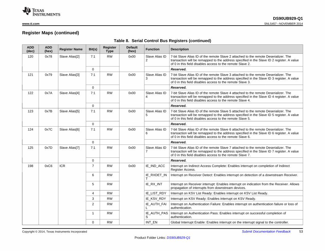
DS90UB929-Q1www.ti.com SNLS457 –NOVEMBER 2014
Register Maps (continued)Table 8. Serial Control Bus Registers (continued)
ADD ADD Register DefaultRegister Name Bit(s) Function Description(dec) (hex) Type (hex)120 0x78 Slave Alias[2] 7:1 RW 0x00 Slave Alias ID 7-bit Slave Alias ID of the remote Slave 2 attached to the remote Deserializer. The
2 transaction will be remapped to the address specified in the Slave ID 2 register. A valueof 0 in this field disables access to the remote Slave 2.
0 Reserved.121 0x79 Slave Alias[3] 7:1 RW 0x00 Slave Alias ID 7-bit Slave Alias ID of the remote Slave 3 attached to the remote Deserializer. The
3 transaction will be remapped to the address specified in the Slave ID 3 register. A valueof 0 in this field disables access to the remote Slave 3.
0 Reserved.122 0x7A Slave Alias[4] 7:1 RW 0x00 Slave Alias ID 7-bit Slave Alias ID of the remote Slave 4 attached to the remote Deserializer. The
4 transaction will be remapped to the address specified in the Slave ID 4 register. A valueof 0 in this field disables access to the remote Slave 4.
0 Reserved.123 0x7B Slave Alias[5] 7:1 RW 0x00 Slave Alias ID 7-bit Slave Alias ID of the remote Slave 5 attached to the remote Deserializer. The
5 transaction will be remapped to the address specified in the Slave ID 5 register. A valueof 0 in this field disables access to the remote Slave 5.
0 Reserved.124 0x7C Slave Alias[6] 7:1 RW 0x00 Slave Alias ID 7-bit Slave Alias ID of the remote Slave 6 attached to the remote Deserializer. The
6 transaction will be remapped to the address specified in the Slave ID 6 register. A valueof 0 in this field disables access to the remote Slave 6.
0 Reserved.125 0x7D Slave Alias[7] 7:1 RW 0x00 Slave Alias ID 7-bit Slave Alias ID of the remote Slave 7 attached to the remote Deserializer. The
7 transaction will be remapped to the address specified in the Slave ID 7 register. A valueof 0 in this field disables access to the remote Slave 7.
0 Reserved.198 0xC6 ICR 7 RW 0x00 IE_IND_ACC Interrupt on Indirect Access Complete: Enables interrupt on completion of Indirect
Register Access.6 RW IE_RXDET_IN Interrupt on Receiver Detect: Enables interrupt on detection of a downstream Receiver.
T5 RW IE_RX_INT Interrupt on Receiver interrupt: Enables interrupt on indication from the Receiver. Allows
propagation of interrupts from downstream devices.4 RW IE_LIST_RDY Interrupt on KSV List Ready: Enables interrupt on KSV List Ready.3 RW IE_KSV_RDY Interrupt on KSV Ready: Enables interrupt on KSV Ready.2 RW IE_AUTH_FAI Interrupt on Authentication Failure: Enables interrupt on authentication failure or loss of
L authentication.1 RW IE_AUTH_PAS Interrupt on Authentication Pass: Enables interrupt on successful completion of
S authentication.0 RW INT_EN Global Interrupt Enable: Enables interrupt on the interrupt signal to the controller.
Copyright © 2014, Texas Instruments Incorporated Submit Documentation Feedback 53
Product Folder Links: DS90UB929-Q1

DS90UB929-Q1SNLS457 –NOVEMBER 2014 www.ti.com
Register Maps (continued)Table 8. Serial Control Bus Registers (continued)
ADD ADD Register DefaultRegister Name Bit(s) Function Description(dec) (hex) Type (hex)199 0xC7 ISR 7 R 0x00 IS_IND_ACC Interrupt on Indirect Access Complete: Indirect Register Access has completed.
6 R IS_RXDET_IN Interrupt on Receiver Detect interrupt: A downstream receiver has been detected.T
5 R IS_RX_INT Interrupt on Receiver interrupt: Receiver has indicated an interrupt request from down-stream device.
4 R IS_LIST_RDY Interrupt on KSV List Ready: The KSV list is ready for reading by the controller.3 R IS_KSV_RDY Interrupt on KSV Ready: The Receiver KSV is ready for reading by the controller.2 R IS_AUTH_FAI Interrupt on Authentication Failure: Authentication failure or loss of authentication has
L occurred.1 R IS_AUTH_PAS Interrupt on Authentication Pass: Authentication has completed successfully.
S0 R INT Global Interrupt: Set if any enabled interrupt is indicated.
240 0xF0 TX ID 7:0 R 0x5F ID0 First byte ID code: "_".241 0xF1 7:0 R 0x55 ID1 Second byte of ID code: "U".242 0xF2 7:0 R 0x42 ID2 Third byte of ID code: "B".243 0xF3 7:0 R 0x39 ID3 Fourth byte of ID code: "9".244 0xF4 7:0 R 0x32 ID4 Fifth byte of ID code: "2".245 0xF5 7:0 R 0x39 ID5 Sixth byte of ID code: “9”.
54 Submit Documentation Feedback Copyright © 2014, Texas Instruments Incorporated
Product Folder Links: DS90UB929-Q1

DS90UB929-Q1www.ti.com SNLS457 –NOVEMBER 2014
9 Application and Implementation
NOTEInformation in the following applications sections is not part of the TI componentspecification, and TI does not warrant its accuracy or completeness. TI’s customers areresponsible for determining suitability of components for their purposes. Customers shouldvalidate and test their design implementation to confirm system functionality.
9.1 Applications InformationThe DS90UB929-Q1, in conjunction with the DS90UB926Q-Q1/DS90UB928Q-Q1deserializer, is intended tointerface between a host (graphics processor) and a display, supporting 24-bit color depth (RGB888) and highdefinition (720p) digital video format. It can receive an 8-bit RGB stream with a pixel clock rate up to 96 MHztogether with four I2S audio streams when paired with the DS90UB940-Q1/DS90UB948-Q1 deserializer.
9.2 Typical ApplicationsBypass capacitors should be placed near the power supply pins. A capacitor and resistor are placed on the PDBpin to delay the enabling of the device until power is stable. See below for typical STP and coax connectiondiagrams.
Copyright © 2014, Texas Instruments Incorporated Submit Documentation Feedback 55
Product Folder Links: DS90UB929-Q1
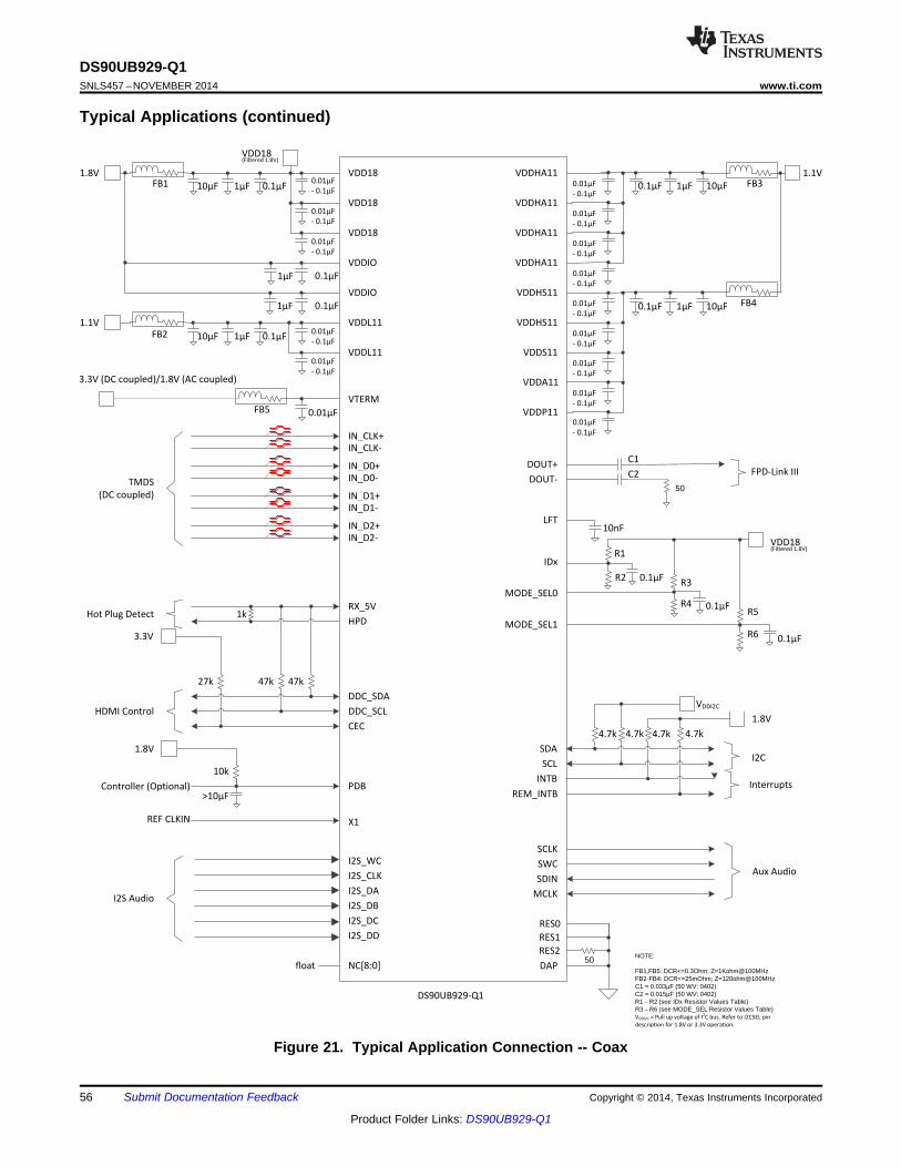
VDD18
VDD18
VDD18
VDDIO
VDDIO
VDDHS11
VDDS11VDDL11
VDDHA11
VDDHA11
VDDHA11
VDDHA11
VDDHS11
IN_CLK+
IN_CLK-
IN_D0+
IN_D0-
IN_D1+
IN_D1-
IN_D2+
IN_D2-
RX_5V
HPD
DDC_SDA
DDC_SCL
CEC
X1
I2S_WC
I2S_CLK
I2S_DA
I2S_DB
I2S_DC
I2S_DD
PDB
NC[8:0]
VDDL11
DAP
1.1V1.8V
1.1V
1.8V
TMDS
(DC coupled)
HDMI Control
I2S Audio
Hot Plug Detect
FB1
FB2
FB3
FB4
>10µF
10k
27k 47k 47k
3.3V
VTERM
3.3V (DC coupled)/1.8V (AC coupled)
FB5
0.01µF
- 0.1µF
0.01µF
- 0.1µF
0.01µF
- 0.1µF
0.1µF
0.1µF
0.01µF
- 0.1µF
0.01µF
- 0.1µF
0.01µF
1µF
1µF
DOUT+
DOUT-
LFT
MODE_SEL0
IDx
MODE_SEL1
SCLK
SWC
SDIN
MCLK
Aux Audio
FPD-Link III
VDD18(Filtered 1.8V)
C1
C2
10nF
R1
R2R3
R4R5
R6
VDDA11
VDDP11
0.01µF
- 0.1µF
0.01µF
- 0.1µF
0.01µF
- 0.1µF
0.01µF
- 0.1µF
0.01µF
- 0.1µF
0.01µF
- 0.1µF
0.01µF
- 0.1µF
0.01µF
- 0.1µF
0.01µF
- 0.1µF
NOTE:
FB1,FB5: DCR<=0.3Ohm; Z=1Kohm@100MHzFB2-FB4: DCR<=25mOhm; Z=120ohm@100MHzC1 = 0.033µF (50 WV; 0402) C2 = 0.015µF (50 WV; 0402) R1 ± R2 (see IDx Resistor Values Table)R3 ± R6 (see MODE_SEL Resistor Values Table)VDDI2C = Pull up voltage of I
2C bus. Refer to I2CSEL pin
description for 1.8V or 3.3V operation.
10µF 1µF
float
0.1µF
0.1µF
0.1µF
Controller (Optional)
10µF 1µF 0.1µF
0.1µF
1µF 10µF0.1µF
1µF 10µF0.1µF
DS90UB929-Q1
REF CLKIN
VDD18(Filtered 1.8V)
SDA
SCL
INTB
1.8V
I2C
4.7k 4.7k 4.7k
VDDI2C
REM_INTB
4.7k
Interrupts
RES2
RES1
RES0
50
50
1k
DS90UB929-Q1SNLS457 –NOVEMBER 2014 www.ti.com
Typical Applications (continued)
Figure 21. Typical Application Connection -- Coax
56 Submit Documentation Feedback Copyright © 2014, Texas Instruments Incorporated
Product Folder Links: DS90UB929-Q1
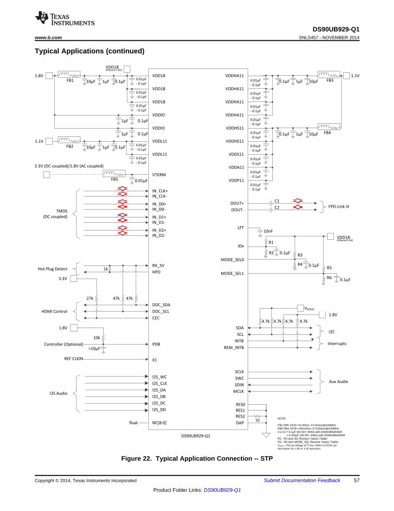
VDD18
VDD18
VDD18
VDDIO
VDDIO
VDDHS11
VDDS11VDDL11
VDDHA11
VDDHA11
VDDHA11
VDDHA11
VDDHS11
IN_CLK+
IN_CLK-
IN_D0+
IN_D0-
IN_D1+
IN_D1-
IN_D2+
IN_D2-
RX_5V
HPD
DDC_SDA
DDC_SCL
CEC
X1
I2S_WC
I2S_CLK
I2S_DA
I2S_DB
I2S_DC
I2S_DD
PDB
NC[8:0]
VDDL11
DAP
1.1V1.8V
1.1V
1.8V
TMDS
(DC coupled)
HDMI Control
I2S Audio
Hot Plug Detect
FB1
FB2
FB3
FB4
>10µF
10k
27k 47k 47k
3.3V
VTERM
3.3V (DC coupled)/1.8V (AC coupled)
FB5
0.01µF
- 0.1µF
0.01µF
- 0.1µF
0.01µF
- 0.1µF
0.1µF
0.1µF
0.01µF
- 0.1µF
0.01µF
- 0.1µF
0.01µF
1µF
1µF
DOUT+
DOUT-
LFT
MODE_SEL0
IDx
MODE_SEL1
SCLK
SWC
SDIN
MCLK
Aux Audio
FPD-Link III
VDD18(Filtered 1.8V)
C1
C2
10nF
R1
R2R3
R4R5
R6
VDDA11
VDDP11
0.01µF
- 0.1µF
0.01µF
- 0.1µF
0.01µF
- 0.1µF
0.01µF
- 0.1µF
0.01µF
- 0.1µF
0.01µF
- 0.1µF
0.01µF
- 0.1µF
0.01µF
- 0.1µF
0.01µF
- 0.1µF
NOTE:
FB1,FB5: DCR<=0.3Ohm; Z=1Kohm@100MHzFB2-FB4: DCR<=25mOhm; Z=120ohm@100MHzC1-C2 = 0.1µF (50 WV; 0402) with DS90UB926/928C1-C2 = 0.033µF (50 WV; 0402) with DS90UB940/948R1 ± R2 (see IDx Resistor Values Table)R3 ± R6 (see MODE_SEL Resistor Values Table)VDDI2C = Pull up voltage of I
2C bus. Refer to I2CSEL pin
description for 1.8V or 3.3V operation.
10µF 1µF
float
0.1µF
0.1µF
0.1µF
Controller (Optional)
10µF 1µF 0.1µF
0.1µF
1µF 10µF0.1µF
1µF 10µF0.1µF
DS90UB929-Q1
REF CLKIN
VDD18(Filtered 1.8V)
SDA
SCL
INTB
1.8V
I2C
4.7k 4.7k 4.7k
VDDI2C
REM_INTB
4.7k
Interrupts
RES2
RES1
RES0
50
1k
DS90UB929-Q1www.ti.com SNLS457 –NOVEMBER 2014
Typical Applications (continued)
Figure 22. Typical Application Connection -- STP
Copyright © 2014, Texas Instruments Incorporated Submit Documentation Feedback 57
Product Folder Links: DS90UB929-Q1

DOUT-
DOUT+
SER
RIN-
RIN+
DES
50Q 50Q
DOUT-
DOUT+
SER
RIN-
RIN+
DES
RGB Display720p
24-bit color depth
TM
DS
Inte
rfac
eMobile Device
/Graphics Processor
FPD-Link III1 Pair / AC Coupled
DS90UB929-Q1Serializer
DS90UB926Q-Q1Deserializer PASS
VDDIO
OSS_SEL
I2C_SCLI2C_SDA
OEN
LOCK
IDxDAP DAP
SCLSDAIDx
R[7:0]
HSVS
PCLKDE
G[7:0]B[7:0]
RIN+
RIN-
DOUT+
DOUT-
1.8V or 3.3V1.8V 1.1V 3.3VVDDIO
I2S AUDIO (STEREO)
3/MODE_SEL
MCLK
PDB
INTB_IN
IN_D0+
IN_D1+
IN_CLK+
IN_D2+
HDMI
4/GPIO
HPDDDCCEC
TMDS ± Transition-Minimized Differential SignalingHDMI ± High Definition Multimedia Interface
DS90UB929-Q1SNLS457 –NOVEMBER 2014 www.ti.com
Typical Applications (continued)
Figure 23. Typical System Diagram
9.2.1 Design RequirementsThe SER/DES supports only AC-coupled interconnects through an integrated DC-balanced decoding scheme.External AC coupling capacitors must be placed in series in the FPD-Link III signal path as illustrated inFigure 24.
Table 9. Design ParametersDESIGN PARAMETER EXAMPLE VALUE
VDDIO 1.8VAC Coupling Capacitor for DOUT0± and DOUT1± with 92x 100nFdeserializersAC Coupling Capacitor for DOUT0± and DOUT1± with 94x 33nF
deserializers
For applications utilizing single-ended 50Ω coaxial cable, the unused data pins (DOUT-) should utilize a 15nFcapacitor and should be terminated with a 50Ω resistor.
Figure 24. AC-Coupled Connection (STP)
Figure 25. AC-Coupled Connection (Coaxial)
For high-speed FPD–Link III transmissions, the smallest available package should be used for the AC couplingcapacitor. This will help minimize degradation of signal quality due to package parasitics.
9.2.2 Detailed Design Procedure
9.2.2.1 High Speed Interconnect GuidelinesSee AN-1108 and AN-905 for full details.
58 Submit Documentation Feedback Copyright © 2014, Texas Instruments Incorporated
Product Folder Links: DS90UB929-Q1
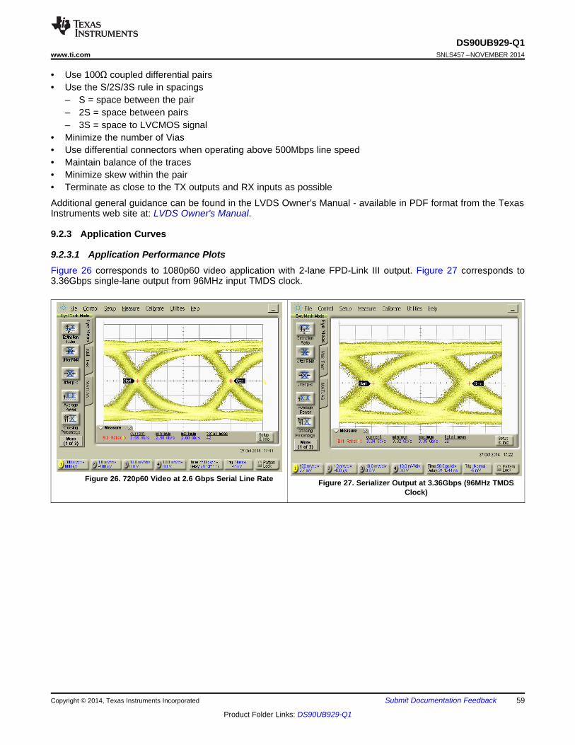
DS90UB929-Q1www.ti.com SNLS457 –NOVEMBER 2014
• Use 100Ω coupled differential pairs• Use the S/2S/3S rule in spacings
– S = space between the pair– 2S = space between pairs– 3S = space to LVCMOS signal
• Minimize the number of Vias• Use differential connectors when operating above 500Mbps line speed• Maintain balance of the traces• Minimize skew within the pair• Terminate as close to the TX outputs and RX inputs as possible
Additional general guidance can be found in the LVDS Owner’s Manual - available in PDF format from the TexasInstruments web site at: LVDS Owner's Manual.
9.2.3 Application Curves
9.2.3.1 Application Performance PlotsFigure 26 corresponds to 1080p60 video application with 2-lane FPD-Link III output. Figure 27 corresponds to3.36Gbps single-lane output from 96MHz input TMDS clock.
Figure 26. 720p60 Video at 2.6 Gbps Serial Line Rate Figure 27. Serializer Output at 3.36Gbps (96MHz TMDSClock)
Copyright © 2014, Texas Instruments Incorporated Submit Documentation Feedback 59
Product Folder Links: DS90UB929-Q1

DS90UB929-Q1SNLS457 –NOVEMBER 2014 www.ti.com
10 Power Supply RecommendationsThis device provides separate power and ground pins for different portions of the circuit. This is done to isolateswitching noise effects between different sections of the circuit. Separate planes on the PCB are typically notrequired. The Pin Functions table provides guidance on which circuit blocks are connected to which power pins.In some cases, an external filter many be used to provide clean power to sensitive circuits such as PLLs.
10.1 Power Up Requirements And PDB PinThe power supply ramp should be faster than 1.5ms with a monotonic rise. A large capacitor on the PDB pin isneeded to ensure PDB arrives after all the supply pins have settled to the recommended operating voltage.When PDB pin is pulled up to VDDIO, a 10kΩ pull-up and a >10μF capacitor to GND are required to delay thePDB input signal rise. All inputs must not be driven until all power supplies have reached steady state.
The recommended power up sequence is as follows: VTERM, VDD18, VDD11, wait until all supplies have settled,activate PDB, then apply HDMI input.
60 Submit Documentation Feedback Copyright © 2014, Texas Instruments Incorporated
Product Folder Links: DS90UB929-Q1

DS90UB929-Q1www.ti.com SNLS457 –NOVEMBER 2014
11 Layout
11.1 Layout GuidelinesCircuit board layout and stack-up for the LVDS serializer and deserializer devices should be designed to providelow-noise power to the device. Good layout practice will also separate high frequency or high-level inputs andoutputs to minimize unwanted stray noise, feedback and interference. Power system performance may be greatlyimproved by using thin dielectrics (2 to 4 mil) for power / ground sandwiches. This arrangement utilizes the planecapacitance for the PCB power system and has low-inductance, which has proven effectiveness especially athigh frequencies, and makes the value and placement of external bypass capacitors less critical. External bypasscapacitors should include both RF ceramic and tantalum electrolytic types. RF capacitors may use values in therange of 0.01μF to 10μF. Tantalum capacitors may be in the 2.2μF to 10μF range. The voltage rating of thetantalum capacitors should be at least 5X the power supply voltage being used.
MLCC surface mount capacitors are recommended due to their smaller parasitic properties. When using multiplecapacitors per supply pin, locate the smaller value closer to the pin. A large bulk capacitor is recommended atthe point of power entry. This is typically in the 50μF to 100μF range and will smooth low frequency switchingnoise. It is recommended to connect power and ground pins directly to the power and ground planes with bypasscapacitors connected to the plane with via on both ends of the capacitor. Connecting power or ground pins to anexternal bypass capacitor will increase the inductance of the path. A small body size X7R chip capacitor, such as0603 or 0805, is recommended for external bypass. A small body sized capacitor has less inductance. The usermust pay attention to the resonance frequency of these external bypass capacitors, usually in the range of20MHz-30MHz. To provide effective bypassing, multiple capacitors are often used to achieve low impedancebetween the supply rails over the frequency of interest. At high frequency, it is also a common practice to usetwo vias from power and ground pins to the planes, reducing the impedance at high frequency.
Some devices provide separate power and ground pins for different portions of the circuit. This is done to isolateswitching noise effects between different sections of the circuit. Separate planes on the PCB are typically notrequired. Pin Description tables typically provide guidance on which circuit blocks are connected to which powerpin pairs. In some cases, an external filter many be used to provide clean power to sensitive circuits such asPLLs. For DS90UB929-Q1, only one common ground plane is required to connect all device related ground pins.
Use at least a four layer board with a power and ground plane. Locate LVCMOS signals away from the LVDSlines to prevent coupling from the LVCMOS lines to the LVDS lines. Closely coupled differential lines of 100Ω aretypically recommended for LVDS interconnect. The closely coupled lines help to ensure that coupled noise willappear as common mode and thus is rejected by the receivers. The tightly coupled lines will also radiate less.
At least 9 thermal vias are necessary from the device center DAP to the ground plane. They connect the deviceground to the PCB ground plane, as well as conduct heat from the exposed pad of the package to the PCBground plane. More information on the LLP style package, including PCB design and manufacturingrequirements, is provided in TI Application Note: AN-1187.
Copyright © 2014, Texas Instruments Incorporated Submit Documentation Feedback 61
Product Folder Links: DS90UB929-Q1

DS90UB929-Q1SNLS457 –NOVEMBER 2014 www.ti.com
11.2 Layout ExampleFigure 28 is derived from a layout design of the DS90UB929-Q1. This graphic is used to demonstrate properhigh-speed routing when designing in the Serializer.
Figure 28. DS90UB929-Q1 Serializer Layout Example
62 Submit Documentation Feedback Copyright © 2014, Texas Instruments Incorporated
Product Folder Links: DS90UB929-Q1
DS90UB929-Q1www.ti.com SNLS457 –NOVEMBER 2014
12 Device and Documentation Support
12.1 Documentation Support
12.1.1 Related DocumentationFor related documentation see the following:• Soldering Specifications Application Report, SNOA549• IC Package Thermal Metrics Application Report, SPRA953• Channel-Link PCB and Interconnect Design-In Guidelines, SNLA008• Transmission Line RAPIDESIGNER Operation and Application Guide, SNLA035• Leadless Leadframe Package (LLP) Application Report, SNOA401• LVDS Owner's Manual, SNLA187• I2C Communication Over FPD-Link III with Bidirectional Control Channel, SNLA131A• Using the I2S Audio Interface of DS90Ux92x FPD-Link III Devices, SNLA221• Exploring the Internal Test Pattern Generation Feature of 720p FPD-Link III Devices, SNLA132
12.2 TrademarksTRI-STATE is a trademark of Texas Instruments.All other trademarks are the property of their respective owners.
12.3 Electrostatic Discharge CautionThese devices have limited built-in ESD protection. The leads should be shorted together or the device placed in conductive foamduring storage or handling to prevent electrostatic damage to the MOS gates.
12.4 GlossarySLYZ022 — TI Glossary.
This glossary lists and explains terms, acronyms, and definitions.
13 Mechanical, Packaging and Orderable InformationThe following pages include mechanical packaging and orderable information. This information is the mostcurrent data available for the designated devices. This data is subject to change without notice and revision ofthis document. For browser-based versions of this data sheet, refer to the left-hand navigation.
Copyright © 2014, Texas Instruments Incorporated Submit Documentation Feedback 63
Product Folder Links: DS90UB929-Q1
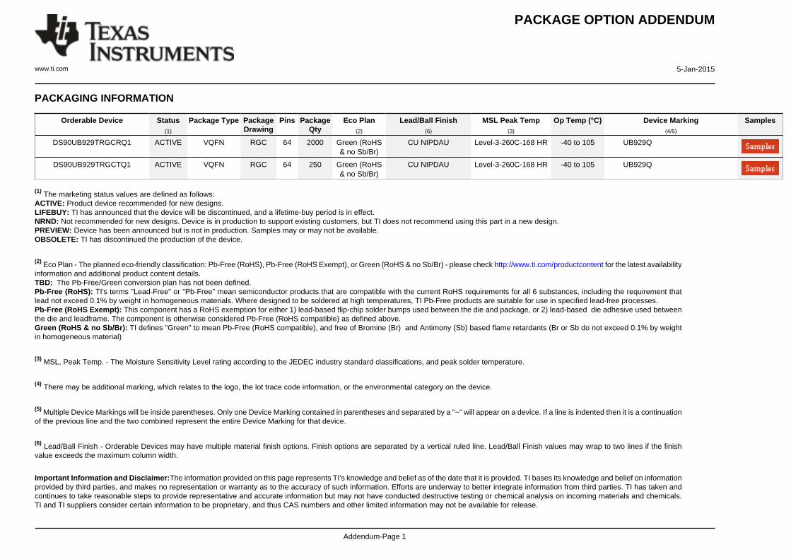
PACKAGE OPTION ADDENDUM
www.ti.com 5-Jan-2015
Addendum-Page 1
PACKAGING INFORMATION
Orderable Device Status(1)
Package Type PackageDrawing
Pins PackageQty
Eco Plan(2)
Lead/Ball Finish(6)
MSL Peak Temp(3)
Op Temp (°C) Device Marking(4/5)
Samples
DS90UB929TRGCRQ1 ACTIVE VQFN RGC 64 2000 Green (RoHS& no Sb/Br)
CU NIPDAU Level-3-260C-168 HR -40 to 105 UB929Q
DS90UB929TRGCTQ1 ACTIVE VQFN RGC 64 250 Green (RoHS& no Sb/Br)
CU NIPDAU Level-3-260C-168 HR -40 to 105 UB929Q
(1) The marketing status values are defined as follows:ACTIVE: Product device recommended for new designs.LIFEBUY: TI has announced that the device will be discontinued, and a lifetime-buy period is in effect.NRND: Not recommended for new designs. Device is in production to support existing customers, but TI does not recommend using this part in a new design.PREVIEW: Device has been announced but is not in production. Samples may or may not be available.OBSOLETE: TI has discontinued the production of the device.
(2) Eco Plan - The planned eco-friendly classification: Pb-Free (RoHS), Pb-Free (RoHS Exempt), or Green (RoHS & no Sb/Br) - please check http://www.ti.com/productcontent for the latest availabilityinformation and additional product content details.TBD: The Pb-Free/Green conversion plan has not been defined.Pb-Free (RoHS): TI's terms "Lead-Free" or "Pb-Free" mean semiconductor products that are compatible with the current RoHS requirements for all 6 substances, including the requirement thatlead not exceed 0.1% by weight in homogeneous materials. Where designed to be soldered at high temperatures, TI Pb-Free products are suitable for use in specified lead-free processes.Pb-Free (RoHS Exempt): This component has a RoHS exemption for either 1) lead-based flip-chip solder bumps used between the die and package, or 2) lead-based die adhesive used betweenthe die and leadframe. The component is otherwise considered Pb-Free (RoHS compatible) as defined above.Green (RoHS & no Sb/Br): TI defines "Green" to mean Pb-Free (RoHS compatible), and free of Bromine (Br) and Antimony (Sb) based flame retardants (Br or Sb do not exceed 0.1% by weightin homogeneous material)
(3) MSL, Peak Temp. - The Moisture Sensitivity Level rating according to the JEDEC industry standard classifications, and peak solder temperature.
(4) There may be additional marking, which relates to the logo, the lot trace code information, or the environmental category on the device.
(5) Multiple Device Markings will be inside parentheses. Only one Device Marking contained in parentheses and separated by a "~" will appear on a device. If a line is indented then it is a continuationof the previous line and the two combined represent the entire Device Marking for that device.
(6) Lead/Ball Finish - Orderable Devices may have multiple material finish options. Finish options are separated by a vertical ruled line. Lead/Ball Finish values may wrap to two lines if the finishvalue exceeds the maximum column width.
Important Information and Disclaimer:The information provided on this page represents TI's knowledge and belief as of the date that it is provided. TI bases its knowledge and belief on informationprovided by third parties, and makes no representation or warranty as to the accuracy of such information. Efforts are underway to better integrate information from third parties. TI has taken andcontinues to take reasonable steps to provide representative and accurate information but may not have conducted destructive testing or chemical analysis on incoming materials and chemicals.TI and TI suppliers consider certain information to be proprietary, and thus CAS numbers and other limited information may not be available for release.
PACKAGE OPTION ADDENDUM
www.ti.com 5-Jan-2015
Addendum-Page 2
In no event shall TI's liability arising out of such information exceed the total purchase price of the TI part(s) at issue in this document sold by TI to Customer on an annual basis.

TAPE AND REEL INFORMATION
*All dimensions are nominal
Device PackageType
PackageDrawing
Pins SPQ ReelDiameter
(mm)
ReelWidth
W1 (mm)
A0(mm)
B0(mm)
K0(mm)
P1(mm)
W(mm)
Pin1Quadrant
DS90UB929TRGCRQ1 VQFN RGC 64 2000 330.0 16.4 9.3 9.3 1.1 12.0 16.0 Q2
DS90UB929TRGCTQ1 VQFN RGC 64 250 180.0 16.4 9.3 9.3 1.1 12.0 16.0 Q2
PACKAGE MATERIALS INFORMATION
www.ti.com 9-May-2018
Pack Materials-Page 1

*All dimensions are nominal
Device Package Type Package Drawing Pins SPQ Length (mm) Width (mm) Height (mm)
DS90UB929TRGCRQ1 VQFN RGC 64 2000 367.0 367.0 38.0
DS90UB929TRGCTQ1 VQFN RGC 64 250 210.0 185.0 35.0
PACKAGE MATERIALS INFORMATION
www.ti.com 9-May-2018
Pack Materials-Page 2

IMPORTANT NOTICE
Texas Instruments Incorporated (TI) reserves the right to make corrections, enhancements, improvements and other changes to itssemiconductor products and services per JESD46, latest issue, and to discontinue any product or service per JESD48, latest issue. Buyersshould obtain the latest relevant information before placing orders and should verify that such information is current and complete.TI’s published terms of sale for semiconductor products (http://www.ti.com/sc/docs/stdterms.htm) apply to the sale of packaged integratedcircuit products that TI has qualified and released to market. Additional terms may apply to the use or sale of other types of TI products andservices.Reproduction of significant portions of TI information in TI data sheets is permissible only if reproduction is without alteration and isaccompanied by all associated warranties, conditions, limitations, and notices. TI is not responsible or liable for such reproduceddocumentation. Information of third parties may be subject to additional restrictions. Resale of TI products or services with statementsdifferent from or beyond the parameters stated by TI for that product or service voids all express and any implied warranties for theassociated TI product or service and is an unfair and deceptive business practice. TI is not responsible or liable for any such statements.Buyers and others who are developing systems that incorporate TI products (collectively, “Designers”) understand and agree that Designersremain responsible for using their independent analysis, evaluation and judgment in designing their applications and that Designers havefull and exclusive responsibility to assure the safety of Designers' applications and compliance of their applications (and of all TI productsused in or for Designers’ applications) with all applicable regulations, laws and other applicable requirements. Designer represents that, withrespect to their applications, Designer has all the necessary expertise to create and implement safeguards that (1) anticipate dangerousconsequences of failures, (2) monitor failures and their consequences, and (3) lessen the likelihood of failures that might cause harm andtake appropriate actions. Designer agrees that prior to using or distributing any applications that include TI products, Designer willthoroughly test such applications and the functionality of such TI products as used in such applications.TI’s provision of technical, application or other design advice, quality characterization, reliability data or other services or information,including, but not limited to, reference designs and materials relating to evaluation modules, (collectively, “TI Resources”) are intended toassist designers who are developing applications that incorporate TI products; by downloading, accessing or using TI Resources in anyway, Designer (individually or, if Designer is acting on behalf of a company, Designer’s company) agrees to use any particular TI Resourcesolely for this purpose and subject to the terms of this Notice.TI’s provision of TI Resources does not expand or otherwise alter TI’s applicable published warranties or warranty disclaimers for TIproducts, and no additional obligations or liabilities arise from TI providing such TI Resources. TI reserves the right to make corrections,enhancements, improvements and other changes to its TI Resources. TI has not conducted any testing other than that specificallydescribed in the published documentation for a particular TI Resource.Designer is authorized to use, copy and modify any individual TI Resource only in connection with the development of applications thatinclude the TI product(s) identified in such TI Resource. NO OTHER LICENSE, EXPRESS OR IMPLIED, BY ESTOPPEL OR OTHERWISETO ANY OTHER TI INTELLECTUAL PROPERTY RIGHT, AND NO LICENSE TO ANY TECHNOLOGY OR INTELLECTUAL PROPERTYRIGHT OF TI OR ANY THIRD PARTY IS GRANTED HEREIN, including but not limited to any patent right, copyright, mask work right, orother intellectual property right relating to any combination, machine, or process in which TI products or services are used. Informationregarding or referencing third-party products or services does not constitute a license to use such products or services, or a warranty orendorsement thereof. Use of TI Resources may require a license from a third party under the patents or other intellectual property of thethird party, or a license from TI under the patents or other intellectual property of TI.TI RESOURCES ARE PROVIDED “AS IS” AND WITH ALL FAULTS. TI DISCLAIMS ALL OTHER WARRANTIES ORREPRESENTATIONS, EXPRESS OR IMPLIED, REGARDING RESOURCES OR USE THEREOF, INCLUDING BUT NOT LIMITED TOACCURACY OR COMPLETENESS, TITLE, ANY EPIDEMIC FAILURE WARRANTY AND ANY IMPLIED WARRANTIES OFMERCHANTABILITY, FITNESS FOR A PARTICULAR PURPOSE, AND NON-INFRINGEMENT OF ANY THIRD PARTY INTELLECTUALPROPERTY RIGHTS. TI SHALL NOT BE LIABLE FOR AND SHALL NOT DEFEND OR INDEMNIFY DESIGNER AGAINST ANY CLAIM,INCLUDING BUT NOT LIMITED TO ANY INFRINGEMENT CLAIM THAT RELATES TO OR IS BASED ON ANY COMBINATION OFPRODUCTS EVEN IF DESCRIBED IN TI RESOURCES OR OTHERWISE. IN NO EVENT SHALL TI BE LIABLE FOR ANY ACTUAL,DIRECT, SPECIAL, COLLATERAL, INDIRECT, PUNITIVE, INCIDENTAL, CONSEQUENTIAL OR EXEMPLARY DAMAGES INCONNECTION WITH OR ARISING OUT OF TI RESOURCES OR USE THEREOF, AND REGARDLESS OF WHETHER TI HAS BEENADVISED OF THE POSSIBILITY OF SUCH DAMAGES.Unless TI has explicitly designated an individual product as meeting the requirements of a particular industry standard (e.g., ISO/TS 16949and ISO 26262), TI is not responsible for any failure to meet such industry standard requirements.Where TI specifically promotes products as facilitating functional safety or as compliant with industry functional safety standards, suchproducts are intended to help enable customers to design and create their own applications that meet applicable functional safety standardsand requirements. Using products in an application does not by itself establish any safety features in the application. Designers mustensure compliance with safety-related requirements and standards applicable to their applications. Designer may not use any TI products inlife-critical medical equipment unless authorized officers of the parties have executed a special contract specifically governing such use.Life-critical medical equipment is medical equipment where failure of such equipment would cause serious bodily injury or death (e.g., lifesupport, pacemakers, defibrillators, heart pumps, neurostimulators, and implantables). Such equipment includes, without limitation, allmedical devices identified by the U.S. Food and Drug Administration as Class III devices and equivalent classifications outside the U.S.TI may expressly designate certain products as completing a particular qualification (e.g., Q100, Military Grade, or Enhanced Product).Designers agree that it has the necessary expertise to select the product with the appropriate qualification designation for their applicationsand that proper product selection is at Designers’ own risk. Designers are solely responsible for compliance with all legal and regulatoryrequirements in connection with such selection.Designer will fully indemnify TI and its representatives against any damages, costs, losses, and/or liabilities arising out of Designer’s non-compliance with the terms and provisions of this Notice.
Mailing Address: Texas Instruments, Post Office Box 655303, Dallas, Texas 75265Copyright © 2018, Texas Instruments Incorporated