![Chapter 5 Passive and Active Current Mirrors · Basic Current Mirrors]tx ]ÉÉÇ ^|Å Dependence of I out on supply, process , and temperature . - Overdrive voltage is the function](https://static.fdocuments.in/doc/165x107/60700ac657d44e0446046c5d/chapter-5-passive-and-active-current-mirrors-basic-current-mirrorstx-.jpg)
High Current, Low Voltage Current Mirrors and …...High Current Low Voltage Current Mirrors and...
14
High Current, Low Voltage Current Mirrors and Applications S. S. RAJPUT 1 AND S. S. JAMUAR 2 lThin Film Technology group, National Physical Laboratory, Dr. K. S. Krishnan Road, New Delhi 110012 India email:[email protected] 2 Department 0/ Electrical Engineering, Indian Institute 0/ Technology, Delhi, New Delhi 110016,India email: [email protected] Abstract. An improved current mirror structure suitable for low voltage analog applications is proposed which has high output impedance (",5 Mn), high bandwidth (",400 MHz), low input «0.4 V) and output compliance voltages «0.5 V) and high output current capability ("'500 IlA). These properties enhance the utility of this type of current mirrors. Applications of these current mirrors in analog circuits are also presented to demonstrate their superiority over their conventional counterpart. PSpice simulations confirm the suitability of the mirror for low voltage analog applications. Key words: Analog VLSI, current mode analog signal processing, current conveyors, trans- conductors, current mirrors. 1. INTRODUCTION Low voltage CMOS analog circuit structures are weIl established now. The requirement for such circuits sterns from the requirements of high circuit density required to incorporate both analog and digital systems on a single chip. Hence, for mixed mode and complex circuit structures, smaller size devices are necessary. The device sizes are shrinking at a fast rate [1] and the threshold voltage of the MOSFET devices cannot be reduced below a certain minimum value. This necessitates investigation into new circuits using high The original version of this chapter was revised: The copyright line was incorrect. This has been corrected. The Erratum to this chapter is available at DOI: © IFIP International Federation for Information Processing 2000 L. M. Silveira et al. (eds.), VLSI: Systems on a Chip 10.1007/978-0-387-35498-9_57
Transcript of High Current, Low Voltage Current Mirrors and …...High Current Low Voltage Current Mirrors and...

High Current, Low Voltage Current Mirrors and Applications
S. S. RAJPUT1 AND S. S. JAMUAR2
lThin Film Technology group, National Physical Laboratory, Dr. K. S. Krishnan Road, New Delhi 110012 India email:[email protected] 2 Department 0/ Electrical Engineering, Indian Institute 0/ Technology, Delhi, New Delhi 110016,India email: [email protected]
Abstract. An improved current mirror structure suitable for low voltage analog applications is proposed which has high output impedance (",5 Mn), high bandwidth (",400 MHz), low input «0.4 V) and output compliance voltages «0.5 V) and high output current capability ("'500 IlA). These properties enhance the utility of this type of current mirrors. Applications of these current mirrors in analog circuits are also presented to demonstrate their superiority over their conventional counterpart. PSpice simulations confirm the suitability of the mirror for low voltage analog applications.
Key words: Analog VLSI, current mode analog signal processing, current conveyors, transconductors, current mirrors.
1. INTRODUCTION
Low voltage CMOS analog circuit structures are weIl established now. The requirement for such circuits sterns from the requirements of high circuit density required to incorporate both analog and digital systems on a single chip. Hence, for mixed mode and complex circuit structures, smaller size devices are necessary. The device sizes are shrinking at a fast rate [1] and the threshold voltage of the MOSFET devices cannot be reduced below a certain minimum value. This necessitates investigation into new circuits using high
The original version of this chapter was revised: The copyright line was incorrect. This has beencorrected. The Erratum to this chapter is available at DOI:
© IFIP International Federation for Information Processing 2000L. M. Silveira et al. (eds.), VLSI: Systems on a Chip
10.1007/978-0-387-35498-9_57
48 s. S. RAJP UTl AND S. S. JAMUAR2
threshold voltage MOS devices, which can operate at low voltages without sacrificing the circuit performance.
In analog circuits, a current mirror (CM) is an essential subsystem block. The overall performance of the analog circuit is dependent on the characteristics of the CM. This has generated the need for design of low voltage (LV) CM with low input and output voltage operation. Almost allhigh swing CMs, which have been reported [2-4] so far, suffers due to the requirements of high voltage at the input end. Some L VCMs have been reported, which require low input voltages [5-7] for their operation. However, these CM structures possess poor frequency response «100MHz) along with lower input current range «100 The demerits ofthese CMs make them unsuitable for use in low voltage high frequency analog and mixed mode signal processing applications such as current conveyors, operational floating amplifiers etc.
In this paper, we propose a LVCM circuit structure based on popular tail current enhancement technique [8,9]. This circuit has capability to operate at lower input voltages «0.5V). The proposed LVCM circuit has been obtained through suitable modifications incorporated in the circuit of [8,9] by using a level shifter [5,7] at their input port. It is possible to obtain composite current outputs (i.e., positive and negative current simultaneously) by suitable modifications in output structure of L VCM. L VCMs, with composite current outputs are normally used in current mode analog signals processing circuits. The operating current range of the modified circuit extends from 1 to 500 with low input «0.4 V) and output «0.5 V) compliance voltages. The proposed L VCMs can operate up to a frequency of 400 MHz for negative output currents. However, for the positive output current the frequency response is in the range of 200 MHz. The proposed LVCM has been used to obtain dass A current conveyor (CC) and voltage to current (V-I) converters.
2. PROPOSED LV CURRENT MIRRORS
2.1 CM Structure
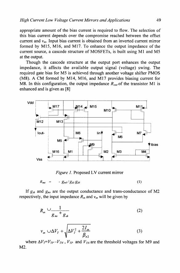
The proposed L VCM circuit structure is shown in Fig. 1. At the input port a PMOS transistor M9 is used to shift the level of gate bias voltage required to operate the input transistor M2 in linear (triode) region. Injection ofthe input current Im into the drain oftransistor M2 causes a voltage (vm), at its drain which is known as the input compliance voltage. The voltage shifter transistor M9 is designed to operate in saturation region for which an
High Current Low Voltage Current Mirrors and Applications 49
appropriate amount of the bias current is required to flow. The selection of this bias current depends over the compromise reached between the offset current and Vm• Input bias current is obtained from an inverted current mirror formed by MI5, MI6, and MI7. To enhance the output impedance ofthe current source, a cascode structure of MOSFETs, is buHt using MI and M5 at the output.
Though the cascode structure at the output port enhances the output impedance, it affects the available output signal (voltage) swing. The required gate bias for M5 is achieved through another voltage shifter PMOS (M8). A CM formed by MI4, MI6, and MI7 provides biasing current for M8. In this configuration, the output impedance Rout of the transistor MI is enhanced and is given as [8]
Vdd
Figure 1. Proposed LV current mirror
(1)
If gdl and gml are the output conductance and trans-conductance of M2 respectively, the input impedance Rm and Vm will be given by
U 1 Rm +
gml gdl (2)
AV: Av:2 21m V m ULl T + Ll T +--
ßn2 (3)
where AVrVTP-VTN, VTP and Vmare the threshold voltages for M9 and M2.
50 s. S. RAJPUTl AND S. S. JAMUAR2
Due to mismatch in the threshold voltages ofthe NMOS and PMOS transistors which are used in the input/output circuits and level shifter; there is an output current known as offset current (IoJjset) for zero input current. The offset current for the circuit of Fig. 1 is given by
I u ßn2 J.r +L\Vr2 +2L\Vrrx1J oJjset 2 II (4)
where,
X=
If vi > > IoJjset can not be decreased below a certain minimum level The offset current is highly dependent on the mismatch between the threshold voltages ofthe input/output NMOS and level shifter PMOS. Smaller the mismatch, lower will be the offset current. However, if VTNand Vrpcan be matched, then can be reduced quite a bit. Thus, IoJjset sets the lower limit of operating currents available from these current mirrors.
2.2 Composite Current Mirror
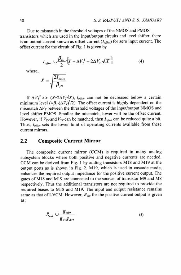
The composite current mirror (CCM) is required in many analog subsystem blocks where both positive and negative currents are needed. CCM can be derived from Fig. 1 by adding transistors M18 and M19 at the output ports as is shown in Fig. 2. M19, which is used in cascode mode, enhances the required output impedance for the positive current output. The gates ofM18 and M19 are connected to the sources oftransistor M9 and M8 respectively. Thus the additional transistors are not required to provide the required biases to M 18 and M 19. The input and output resistance remains same as that of L VCM. However, R out for the positive current output is given as:
(5)
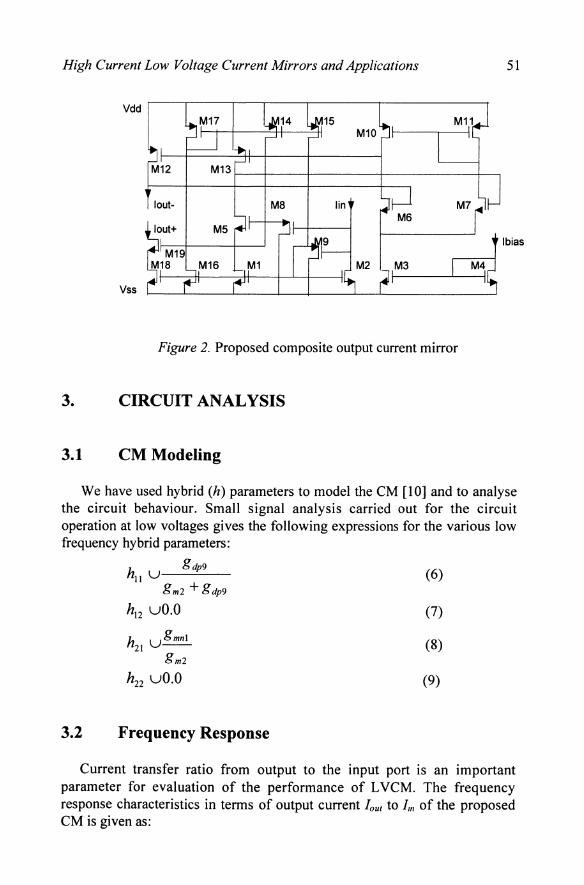
High Current Low Voltage Current Mirrors and Applications 51
Vdd
Ibias
Vss
Figure 2. Proposed composite output current mirror
3. CIRCUIT ANALYSIS
3.1 CM Modeling
We have used hybrid (h) parameters to model the CM [10] and to analyse the circuit behaviour. Small signal analysis carried out for the circuit operation at low voltages gives the following expressions for the various low frequency hybrid parameters:
hll U gdp9
(6) gm2 + gdp9
h12 uO.O (7)
h u gmnl 21 -- (8)
gm2
h22 uO.O (9)
3.2 Frequency Response
Current transfer ratio from output to the input port is an important parameter for evaluation of the performance of L VCM. The frequency response characteristics in terms of output current loul to Im of the proposed CM is given as:

52 s. S. RAJPUTI AND S. S. JAMUAR2
sCgdPO 1+--
lout(s) u gmpo H(s) l (s) s(2Cx +Cgdpo )
In 1 + -----.::'-'--gmpo
(10)
where C gdpo, and gmpo, represent the gate to drain capacitance and transconductance for M12 or M13 respectively. Cx and H(s) are representing the stray capacitance associated at the gate of M7 and the current transfer function for the input circuit formed by MI, M2, M3, M8 and M9. Generally H(s) is frequency independent and taking it to be unity, equation (10) reduces to:
sCgdpo 1+--
lout(s) gmpo .....:..::'--'- U lin(s) 1+ s(2Cx +Cgdpo )
gmpo
(11)
As can be seen from the equation (11), the stray capacitance (Cx) severely degrades the high frequency response for the proposed L VCM.
3.3 Sensitivity Analysis
Sensitivity is one of the most important criteria used for comparing the circuit performance. We shall evaluate the sensitivity of the output current over the circuit parameters such as device dimensions and circuit structure. The sensitivity ofthe output current with respect to h,Qsl and dVris given as:
(12)
slour U 2ßmt1.Vr 6Vr ST10UT
6Vr
(13)
where the stability factors are represented as:
(14)
High Current Low Voltage Current Mirrors and Applications 53
and,
(15)
As can be seen from the above expressions that the stability factors are quite high (> 1 03) for the proposed circuit structures. This in turn results in low sensitivity «10-5) ofthe output current to the variations ofthe circuit (ß" and ßp) and device parameters (L\Vr).
3.4 Simulation Results
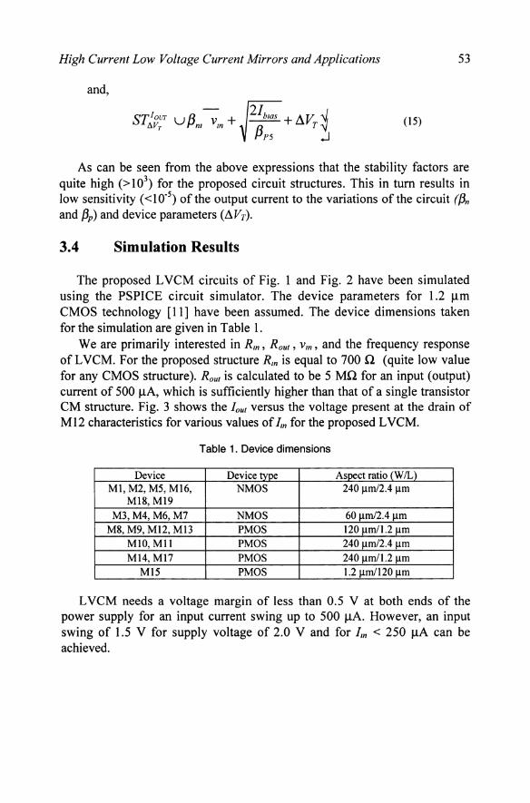
The proposed L VCM circuits of Fig. 1 and Fig. 2 have been simulated using the PSPICE circuit simulator. The device parameters for 1.2 CMOS technology [11] have been assumed. The device dimensions taken for the simulation are given in Table 1.
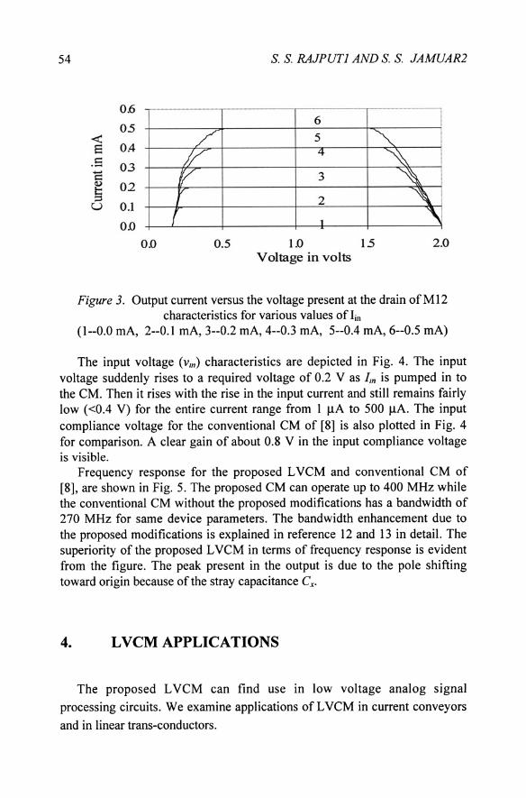
We are primarily interested in R m , R out , Vm , and the frequency response ofLVCM. For the proposed structure Rm is equal to 700 n (quite low value for any CMOS structure). R out is calculated to be 5 Mn for an input (output) current of 500 which is sufficiently higher than that of a single transistor CM structure. Fig. 3 shows the lout versus the voltage present at the drain of M12 characteristics for various values of Im for the proposed LVCM.
Table 1. Device dimensions
Device Device type Aspect ratio (WIL) 240 ,.un/2.4 Ilffi
60 Ilml2.4 Ilffi 120 Ilml1.21lffi 240 Ilml2.4 Ilffi 240 Ilml1.2 Ilffi 1.2 Ilml120 Ilffi
L VCM needs a voltage margin of less than 0.5 V at both ends of the power supply for an input current swing up to 500 However, an input swing of 1.5 V for supply voltage of 2.0 V and for Im < 250 can be achieved.
54 s. S. RAJPUTl AND S. S. JAMUAR2
0.6
05 < E 0.4 .s 03 -c g 02 ='
U 0.1
0.0
-_._. __ _······-1 6
/' 5 "" I // q I , , !f 3 , I
i I r 2 "' r 1 '\
0.0 0.5 1.0 15 2.0 Voltage in volts
Figure 3. Output current versus the voltage present at the drain ofM12 characteristics for various values of liD
(1--0.0 mA, 2--0.1 mA, 3--0.2 mA, 4--0.3 mA, 5--0.4 mA, 6--0.5 mA)
The input voltage (vm) characteristics are depicted in Fig. 4. The input voltage suddenly rises to a required voltage of 0.2 V as Im is pumped in to the CM. Then it rises with the rise in the input current and still remains fairly low «0.4 V) for the entire current range from 1 IlA to 500 1lA. The input compliance voltage for the conventional CM of [8] is also plotted in Fig. 4 for comparison. A clear gain of about 0.8 V in the input compliance voltage is visible.
Frequency response for the proposed L VCM and conventional CM of [8], are shown in Fig. 5. The proposed CM can operate up to 400 MHz while the conventional CM without the proposed modifications has a bandwidth of 270 MHz for same device parameters. The bandwidth enhancement due to the proposed modifications is explained in reference 12 and 13 in detail. The superiority of the proposed L VCM in terms of frequency response is evident from the figure. The peak present in the output is due to the pole shifting toward origin because of the stray capacitance C.
4. LVCM APPLICATIONS
The proposed L VCM can find use in low voltage analog signal processing circuits. We examine applications of L VCM in current conveyors and in linear trans-conductors.

High Current Low Vo/tage Current Mirrors and Applications
s Ö >
1.5
.5 1.0
0.5
..s 0.0
r--' _.
0 .0 0 .1 0.2 0.3 0.4
Input current in mA
Figure 4. Input voltage characteristics
1
?
05
(1 - Conventional mirror [8] and 2 - Proposed LV CM)
In
.5 c
-c
0. 1 1.0 10.0
Frequency in Mt-
100.0 1000.0
55
Figure 5. Simulated frequency response characteristics (l-Conventional CM [8], 2-Proposed L VCM for positive current output
and 3--- for negative current output).
4.1 Current Conveyor 11
LVCM discussed in the previous section has been used for the design of a dass A CMOS current conveyor III (CCIII) ofthe type discussed in [14, 15]. For rail to rail operation of this type of CCIIIs, low input voltage CMs are
necessary.
56 S. S. RAJPUTJ AND S. S. JAMUAR2
4.1.1 Circuit Implementation
The circuit diagram of a proposed CCIII is shown in Fig. 6. The voltage transfer from port Y to port X takes place as the LVCMI forces the equal current to flow through MI and M2. When the aspect ratio (W/L) of the transistor are kept to ensure ßnl={3p2, the drop across gate source terminals of MI and M2 will be equal, which in turn transfer the voltage applied at the drain of MI to the source terminal of M2. Current transfer from port X to port Y is achieved through the action ofLVCMI and LVCM2.
\Ss
Vy G)4Iy-+--I M1
-laut -+laut LVCM1
LVCM2
\Ss
Figure 6. Proposed CCIII structure.
As evident from the figure the input signal can swing raH to raH for the positive inputs however, for negative voltages the input voltage swing is restricted to:
(16)
When VCM is very low as in the case of proposed L VCM, the swing range increases approximately by 0.8V (the difference in the input voltage of proposed and conventional CMs).
4.1.2 Simulation ResuIts
P-Spice simulations were carried out for CCIII structure. The aspect ratio for transistor MI and M2 were taken to be 60 J..lm/1.2 J..lm and 240 J..lm/1.2 J..lm for NMOS and PMOS transistors respectively. The bias voltages are taken to be ±1.0 V. The output characteristics for the input current swing are
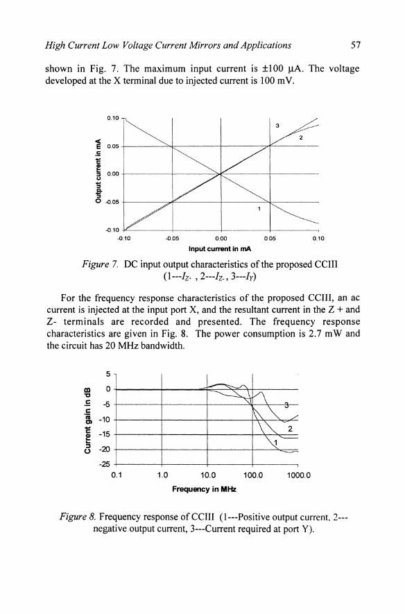
High Current Low Voltage Current Mirrors and Applications 57
shown in Fig. 7. The maximum input current is ±100 /J.A. The voltage developed at the X terminal due to injected current is 100 mV.
0.10 3
1 0.05 .5 1:
0.00 = u :; ! o -{I.05
-{I.l0 -+"-----f-----f------+----.........., -{I.l0 -{I.05 0.00 0.05 0.10
Input current in mA
Figure 7. DC input output characteristics of the proposed CCIII (l---lz+ , 2---lz-, 3---Ir)
For the frequency response characteristics of the proposed CCIII, an ac current is injected at the input port X, and the resultant current in the Z + and Z- terminals are recorded and presented. The frequency response characteristics are given in Fig. 8. The power consumption is 2.7 mW and the circuit has 20 MHz bandwidth.
m "tJ
.E c ii m C I!! ... :I 0
5
0
-5
-10
-15
-20
-25 0.1 1.0
"\ ... "" " /
\ "" 2 .. -
10.0 100.0 1000.0
Frequency in MHz
Figure 8. Frequency response ofCCIII (l---Positive output current, 2--negative output current, 3---Current required at port V).
58 S. S. RAJPUTI AND S. S. JAMUAR2
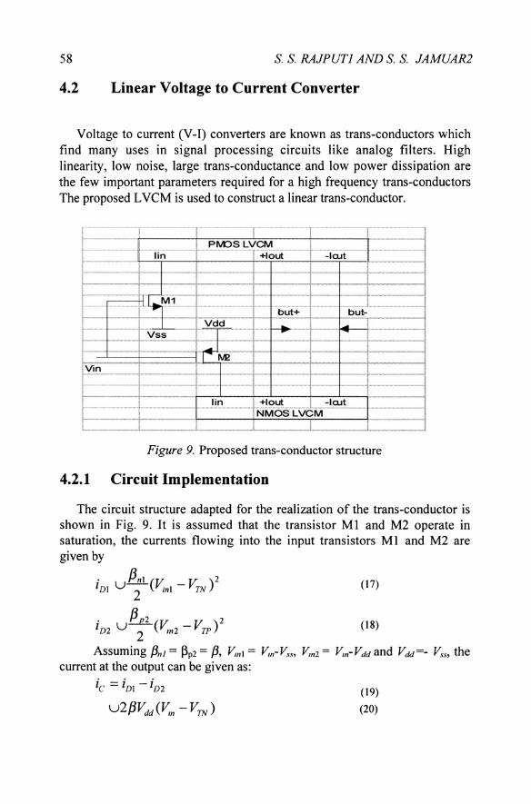
4.2 Linear Voltage to Current Converter
Voltage to current (V-I) converters are known as trans-conductors which find many uses in signal processing circuits Iike analog filters. High linearity, low noise, large trans-conductance and low power dissipation are the few important parameters required for a high frequency trans-conductors The proposed L VCM is used to construct a linear trans-conductor.
·---------·-T .-----... --
r-----. --li-n--'-
I I
-I- _ .... __ but+ but- ·---· .... -····-
,-- -----... ... -.. ----- .---+-.... ----. ---f4-- - .... -
1M2 ._--1----1
1-- ----
Figure 9. Proposed trans-conductor structure
4.2.1 Circuit Implementation
The circuit structure adapted for the realization of the trans-conductor is shown in Fig. 9. It is assumed that the transistor MI and M2 operate in saturation, the currents flowing into the input transistors MI and M2 are given by
. ßnl (V V)2 (17) IDl U--- inl - TN 2
. &(V V)2 ID2 U m2 - TP 2
(18)
Assuming ßnl = ßp2 = ß, = Vm2 = and Vdd =- Vss, the CUTTent at the output can be given as:
(19)
(20)

High Current Low Voltage Current Mirrors and Applications 59
Examination of the above equation yields that the trans-conductor will show a linear characteristic and the trans-conductance can be varied by suitably chosen values of ß and/or supply voltages.
4.2.2 Simulation Results
For PSpice simulations of above trans-conductor, the aspect ratio for transistor MI and M2 were taken to be 7.2 /lm/2.4 /lm and 30.6 /lm/2.4 /lm for NMOS and PMOS transistors respectively. The substrate contacts of these MOSFETs are assumed to be connected to the most positive terminal for the PMOS and the most negative terminal for the NMOS respectively and the supply voltages of±l.O V are taken for all simulations.
Output current versus input voltage characteristics of the circuit is depicted in Fig. 10 in which its rail to rail input voltage swing capability is evident. The trans-conductor consumes 0.6 m W power.
0.20
« 0.15 E .S 0.10
1: 0.05 !
0.00 u
-0.05 ,e. 5 -0.10
-0.15
-020
,..-._ ... _---
r-....
r-....
-------- ----------/ L
v
-1.0 -0.5 0.0
Input voltage in volts
1 /'
/ .,/
/""
.......... .......... 2
.........
0.5 1.0
Figure 10. V-I conversion characteristics (l-Iout+ and 2---Iout-)
5. CONCLUSIONS
Wehave presented a modified low voltage, current mirror structure, capable of giving high input and output voltage swings. The operating current range of the L VCM extends from 1 /lA to 500 /lA with a bandwidth as high as 200 MHz. The input voltage requirement is also quite small «0.4 V). The usefulness of the proposed L VCM over its conventional part of [8] makes it an attractive candidate for low voltage analog design.
The superiority of these L VCMs when used in the current conveyor structures and linear trans-conductor structures is also significant. The resultant CCIII and trans-conductor structures consume very low power and
60 s. S. RAJPUTl AND S. S. JAMUAR2
can operate at sufficiently low voltages present at the input port. Thus the proposed L VCM can be used for low voltage, analog circuit applications.
6. ACKNOWLEDGEMENT
One of the author (S. S. Rajput) expresses his gratitude to Dr. R. Bhattacharyya, Head, Thin Film Technology Group, NPL and to Prof. A. K. Raychodhury, Director NPL New Delhi, for their constant encouragement, and keen interest in the work.
7. REFERENCES
[1] Y. Taur, D. A. Buchanan, W. Chen, D. J. Frank, K. E. Ismail, S. Lo, G. A. Sai-halisz, R. G. Vishvanathan, H. C. Wann, S. 1. Wind, and H. Wang, "CMOS scaling into the nano-meter regime", Proc. IEEE, April 1997, 486-504. [2] J. Mulder, A. C. Woerd, W. A. Serdian, and A. H. M Roermund, "High swing cascode MOS current mirror", Electron Lett. , 4th July, 1996,32, 1251-1252 [3] E. Sackinger, and W. Guggenbuhl, "A high swing, high impedance MOS cascode current mirror", IEEE 1. Solid State Circuits, Feb. 1990,25,289-298 [4] A. Zeki, and H. Kuntman, "Accurate and high output impedance current mirrors suitable for CMOS current output stages", Electron Lett. ,5th June 1997, 33, 1042-1043 [5J V. 1. Proddanov, and M M Green, "eMOS current mirrors with reduced input and output voltage requirements", Electron Lett. ,18th Jan. 1996,32, 104-105 [6] P. Heim, and M. A. Jabri, "MOS cascode-current mirror biasing circuit operating at any current level with minimal output saturation voltage", Electron Lett, 1995,31,690-691 [7] B. J. Blalock, P. E. Allen, and A. R. Gariel, "Designing I-V Op Amps using standard digital CMOS technology", IEEE Trans. Circuits and Systems-I, July 1998,45,769-780. [8] F. You, S. H. K. Embabi, J. F. Duque-Carrilo, and E. Sanchez-Sinencio, "An improved tail current source for low voltage applications", IEEE J. Solid State Circuits, Aug. 1997, 37(8),1173-1179 [9] E. Seevinck, M Plessis, T. Joubert, and A. E. Theron, "Active bootstrapped gain enhancement technique for low voltage circuits", IEEE Trans. Circuits Systems-lI, Sept. 1998,45(9), 1250-1254 [10] Jaeger, R. c., Microelectronics Circuit Design, Mc-Graw Hili, New York, 1997 [11] Silval-Martinez, J., Steyaert, M., Sansen, W., High performance CMOS continuous time filters, Kluwer Academic Publishers, Boston, 1993 [12] T. Voo, and C. Toumazau, 'High speed current mirror resistive compensation technique', Electron Lett., 1995, 31 , no. 4, pp. 248-250 [13] T. Voo, and C. Toumazau, "Precision temperature stabilized tunable CMOS current mirror for filter applications", Electron Lett., 1996,32, no. 2, pp. 105-106
[14] H. W. Cha, and K. Watanabe, "Wide band CMOS current conveyor", Electron Lelt., vol. 32, no. 14, pp. 1245 -1246, 4th July 1996 [15] S. S. Rajput, and S. S. Jamuar, "A new wide bandwidth current controlled CMOS current conveyor III implementation," reported to Electronics letters.