Hi-fi Stereo/mono Infrared Transmitter and Stereo Sub...
28
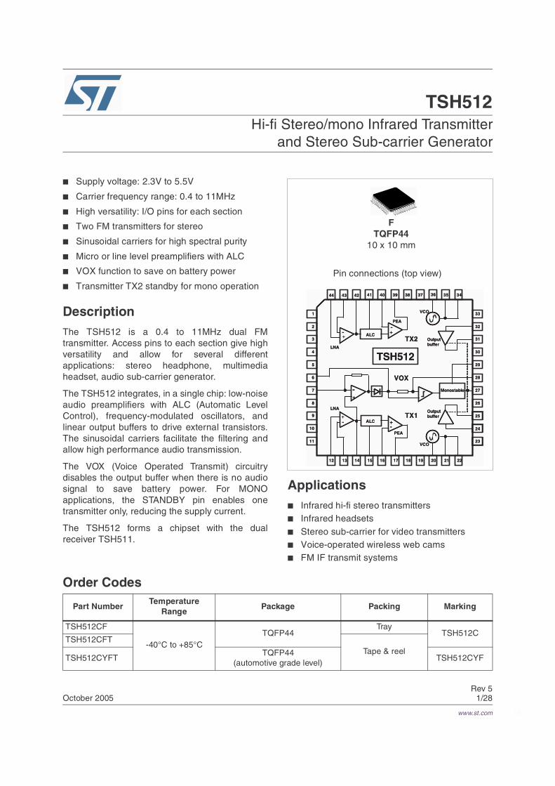
Rev 5 28 October 2005 1/28 TSH512 Hi-fi Stereo/mono Infrared Transmitter and Stereo Sub-carrier Generator ■ Supply voltage: 2.3V to 5.5V ■ Carrier frequency range: 0.4 to 11MHz ■ High versatility: I/O pins for each section ■ Two FM transmitters for stereo ■ Sinusoidal carriers for high spectral purity ■ Micro or line level preamplifiers with ALC ■ VOX function to save on battery power ■ Transmitter TX2 standby for mono operation Description The TSH512 is a 0.4 to 11MHz dual FM transmitter. Access pins to each section give high versatility and allow for several different applications: stereo headphone, multimedia headset, audio sub-carrier generator. The TSH512 integrates, in a single chip: low-noise audio preamplifiers with ALC (Automatic Level Control), frequency-modulated oscillators, and linear output buffers to drive external transistors. The sinusoidal carriers facilitate the filtering and allow high performance audio transmission. The VOX (Voice Operated Transmit) circuitry disables the output buffer when there is no audio signal to save battery power. For MONO applications, the STANDBY pin enables one transmitter only, reducing the supply current. The TSH512 forms a chipset with the dual receiver TSH511. Applications ■ Infrared hi-fi stereo transmitters ■ Infrared headsets ■ Stereo sub-carrier for video transmitters ■ Voice-operated wireless web cams ■ FM IF transmit systems Order Codes 2 3 4 5 6 7 8 9 10 11 12 13 14 15 16 17 18 19 20 21 22 23 24 25 26 27 28 29 30 31 32 33 34 35 36 37 38 39 40 41 42 43 44 1 + - + - + - + - TSH512 Monostable ALC ALC VCO VCO Output buffer Output buffer TX1 TX2 LNA LNA VOX - + PEA PEA 2 3 4 5 6 7 8 9 10 11 12 13 14 15 16 17 18 19 20 21 22 23 24 25 26 27 28 29 30 31 32 33 34 35 36 37 38 39 40 41 42 43 44 1 - + - + - + TSH512 Monostable ALC ALC VCO VCO Output buffer Output buffer TX1 TX2 LNA LNA VOX - + PEA PEA Pin connections (top view) F TQFP44 10 x 10 mm Part Number Temperature Range Package Packing Marking TSH512CF -40°C to +85°C TQFP44 Tray TSH512C TSH512CFT Tape & reel TSH512CYFT TQFP44 (automotive grade level) TSH512CYF www.st.com
Transcript of Hi-fi Stereo/mono Infrared Transmitter and Stereo Sub...
Rev 5
28
October 2005 1/28
TSH512Hi-fi Stereo/mono Infrared Transmitter
and Stereo Sub-carrier Generator
Supply voltage: 2.3V to 5.5V
Carrier frequency range: 0.4 to 11MHz
High versatility: I/O pins for each section
Two FM transmitters for stereo
Sinusoidal carriers for high spectral purity
Micro or line level preamplifiers with ALC
VOX function to save on battery power
Transmitter TX2 standby for mono operation
DescriptionThe TSH512 is a 0.4 to 11MHz dual FMtransmitter. Access pins to each section give highversatility and allow for several differentapplications: stereo headphone, multimediaheadset, audio sub-carrier generator.
The TSH512 integrates, in a single chip: low-noiseaudio preamplifiers with ALC (Automatic LevelControl), frequency-modulated oscillators, andlinear output buffers to drive external transistors.The sinusoidal carriers facilitate the filtering andallow high performance audio transmission.
The VOX (Voice Operated Transmit) circuitrydisables the output buffer when there is no audiosignal to save battery power. For MONOapplications, the STANDBY pin enables onetransmitter only, reducing the supply current.
The TSH512 forms a chipset with the dualreceiver TSH511.
Applications Infrared hi-fi stereo transmitters Infrared headsets Stereo sub-carrier for video transmitters Voice-operated wireless web cams FM IF transmit systems
Order Codes
2
3
4
5
6
7
8
9
10
11
12 13 14 15 16 17 18 19 20 21 22
23
24
25
26
27
28
29
30
31
32
33
3435363738394041424344
1
+- +
-
+- +
-
TSH512
Monostable
ALC
ALC
VCO
VCO
Outputbuffer
Outputbuffer
TX1
TX2LNA
LNA
VOX
-+
PEA
PEA2
3
4
5
6
7
8
9
10
11
12 13 14 15 16 17 18 19 20 21 22
23
24
25
26
27
28
29
30
31
32
33
3435363738394041424344
1
-- +-+-
+
TSH512
Monostable
ALC
ALC
VCO
VCO
Outputbuffer
Outputbuffer
TX1
TX2LNA
LNA
VOX
-+
PEA
PEA
Pin connections (top view)
FTQFP44
10 x 10 mm
Part NumberTemperature
RangePackage Packing Marking
TSH512CF
-40°C to +85°CTQFP44
TrayTSH512C
TSH512CFTTape & reel
TSH512CYFTTQFP44
(automotive grade level)TSH512CYF
www.st.com

Absolute Maximum Ratings TSH512
2/28
1 Absolute Maximum Ratings
Table 1. Key parameters and their absolute maximum ratings
Table 2. Operating conditions
Symbol Parameter Value Unit
Vcc Supply voltage(1)
1. All voltages values, except differential voltage, are with respect to network ground terminal
7 V
Toper Operating free air temperature range -40 to +85 °C
Tstg Storage temperature -65 to +150 °C
Tj Maximum junction temperature 150 °C
Rthjc Thermal resistance junction to case 14 °C/W
Rthja Thermal resistance junction to ambient area 45 °C/W
Latch-up Class(2)
2. Corporate ST Microelectronics procedure number 0018695
A
ESD sensitive device: handling precautions required
ESDexcept pin 20 & 36
HBM: Human Body Model(3)
CDM: Charged Device Model(4)
MM: Machine Model(5)
3. ElectroStatic Discharge pulse (ESD pulse) simulating a human body discharge of 100 pF through 1.5kΩ
4. Discharge to Ground of a device that has been previously charged.
5. ElectroStatic Discharge pulse (ESD pulse) approximating a pulse of a machine or mechanical equipment.
21
0.2kV
Symbol Parameter Value Unit
Vcc Supply voltage 2.3 to 5.5 V
faudio Audio frequency range 20 to 20,000 Hz
fcarrier Carrier frequency range 0.4 to 11 MHz

TSH512 Device diagrams and schematics
3/28
2 Device diagrams and schematics
This chapter contains a detailed block diagram of the TSH512 (Figure 1), with an accompanying pin description (Table 3 on page 4), as well as a typical application schematic (Figure 2 on page 6).
Figure 1. Block diagram
2
3
4
5
6
7
8
9
10
11
12 13 14 15 16 17 18 19 20 21 22
23
24
25
26
27
28
29
30
31
32
33
3435363738394041424344
1
+- +
-
+- +
-
TSH512
Monostable
ALC
ALC
VCO
VCO
Outputbuffer
Outputbuffer
TX1
TX2LNA
LNA
VOX
-+
PEA
PEA2
3
4
5
6
7
8
9
10
11
12 13 14 15 16 17 18 19 20 21 22
23
24
25
26
27
28
29
30
31
32
33
3435363738394041424344
1
-- +-+-
+
TSH512
Monostable
ALC
ALC
VCO
VCO
Outputbuffer
Outputbuffer
TX1
TX2LNA
LNA
VOX
-+
PEA
PEA
VC
O-B
IAS
2
VC
O-O
UT2
LNA
-INP
2
LNA
-INN
2
LNA
-OU
T2
ALC
-INT2
PE
A-IN
N2
PE
A-O
UT2
VC
C
VC
O-A
2
VC
O-B
2
VC
O-B
IAS
2
VC
O-O
UT2
LNA
-INP
2
LNA
-INN
2
LNA
-OU
T2
ALC
-INT2
PE
A-IN
N2
PE
A-O
UT2
VC
C
VC
O-A
2
VC
O-B
2
DEC2
MIC-BIAS2
GND
VCC
SBY
VOX-INTS
VOX-SENS
VCC
GND
MIC-BIAS1
DEC1
DEC2
MIC-BIAS2
GND
VCC
SBY
VOX-INTS
VOX-SENS
VCC
GND
MIC-BIAS1
DEC1
GND
BUF-IN2
BUF-OUT2
GND
VOX-TIMER
VOX-INTN
VOX-MUTE
VCC
BUF-OUT1
BUF-IN1
GND
GND
BUF-IN2
BUF-OUT2
GND
VOX-TIMER
VOX-INTN
VOX-MUTE
VCC
BUF-OUT1
BUF-IN1
GND
LNA
-INP
1
LNA
-INN
1
LNA
-OU
T1
ALC
-INT1
PE
A-IN
N1
PE
A-O
UT1
VC
O-B
IAS
1
VC
C
VC
O-A
1
VC
O-B
1
VC
O-O
UT1
LNA
-INP
1
LNA
-INN
1
LNA
-OU
T1
ALC
-INT1
PE
A-IN
N1
PE
A-O
UT1
VC
O-B
IAS
1
VC
C
VC
O-A
1
VC
O-B
1
VC
O-O
UT1

Device diagrams and schematics TSH512
4/28
Table 3. Pin descriptions
Pin Pin name Related to Direction(1) Pin description
1 DEC2 TX2 - Decoupling capacitor for internal voltage reference
2 MIC-BIAS2 TX2 O Microphone bias
3 GND - - GROUND
4 VCC - - SUPPLY VOLTAGE
5 SBY TX1 & TX2 I Standby Control (INPUT pin)
6 VOX-INTS TX1 & TX2 - Time constant terminal for Audio Signal integrator in VOX
7 VOX-SENS TX1 & TX2 - Gain adjustment for VOX input sensitivity
8 VCC - - SUPPLY VOLTAGE
9 GND - - GROUND
10 MIC-BIAS1 TX1 O Microphone bias
11 DEC1 TX1 - Decoupling capacitor for internal voltage reference
12 LNA-INP1 TX1 I LNA positive input
13 LNA-INN1 TX1 I LNA negative input
14 LNA-OUT1 TX1 O LNA output
15 ALC-INT1 TX1 - Time constant terminal for integrator in ALC
16 PEA-INN1 TX1 I Pre-Emphasis Amplifier negative input
17 PEA-OUT1 TX1 O Pre-Emphasis Amplifier output
18 VCO-BIAS1 TX1 O Bias for external VCO components
19 VCC - - Supply Voltage
20 VCO-A1 TX1 - Oscillator component connection
21 VCO-B1 TX1 - Oscillator component connection
22 VCO-OUT1 TX1 O VCO output
23 GND - - Ground
24 BUF-IN1 TX1 I Input to the output buffer
25 BUF-OUT1 TX1 O Output of the output buffer
26 VCC - - Supply Voltage
27 VOX-MUTE TX1 & TX2 O Mute control (Output pin) in VOX
28 VOX-INTN TX1 & TX2 - Time constant terminal for Noise integrator in VOX
29 VOX-TIMER TX1 & TX2 - Rise time for timer in VOX
30 GND - - Ground
31 BUF-OUT2 TX2 O Output of the output buffer
32 BUF-IN2 TX2 I Input to the output buffer
33 GND - - Ground
34 VCO-OUT2 TX2 O VCO output
35 VCO-B2 TX2 - Oscillator component connection

TSH512 Device diagrams and schematics
5/28
36 VCO-A2 TX2 - Oscillator component connection
37 VCC - - Supply Voltage
38 VCO-BIAS2 TX2 O Bias for external VCO components
39 PEA-OUT2 TX2 O Pre-Emphasis Amplifier output
40 PEA-INN2 TX2 I Pre-Emphasis Amplifier negative input
41 ALC-INT2 TX2 - Time constant terminal for internal peak detector in ALC
42 LNA-OUT2 TX2 O LNA output
43 LNA-INN2 TX2 I LNA negative input
44 LNA-INP2 TX2 I LNA positive input
1. Pin directions: I = input pin, O = output pin, - = pin to connect to supply or decoupling capacitors or external components
Table 3. Pin descriptions
Pin Pin name Related to Direction(1) Pin description

Device diagrams and schematics TSH512
6/28
Figure 2. Typical application schematic for stereo infrared transmitter

TSH512 Electrical Characteristics
7/28
3 Electrical Characteristics
Table 4. Electrical characteristics for VCC = 2.7V, Tamb = 25°C, faudio = 1kHz, fcarrier = 2.8MHz (unless otherwise specified)
Symbol Parameter Test condition Min. Typ. Max. Unit
Overall Circuit
ICC_TOTCurrent consumptionTX1 and TX2 are on
TX1 on, TX2 on, MIC-BIAS1 and MIC-BIAS2 not used:
VOX-MUTE=1 output buffers onVOX-MUTE=0, output buffers off
1611
18.612.8
mA
ICC_SBY
Current consumption with TX2 in stand-by: SBY (pin5) active
TX1 on, TX2 off, MIC-BIAS1 and MIC-BIAS2 not used:
VOX-MUTE=1,output buffers onVOX-MUTE=0, output buffers off
107
11.58
mA
LNA Sections (for TX1 and TX2)
GBPLNA Gain Band Product No external load 7 MHz
RinLNA
Input Resistance on positive input:
(LNA-INP1 pin 12 or LNA-INP2 pin 44)
30 kΩ
THDLNA Total Harmonic Distortion GLNA = 0dB VoutLNA = 700mVPP 0.01 0.05 %
EnEquivalent Input Noise Voltage
GLNA=40dB, at f=1kHzRs = 390Ω, Rfeedback = 39kΩ
6 nV/√Hz
Automatic Level Control (ALC) Section
GALC Voltage Gain 20 dB
VALC_OUT
Regulated Output Level(at positive input of the PEA amplifier)
600 710 800 mVpp
Pre-Emphasis Amplifier (PEA) Section
GBPPEA
Gain Band Product(PEA-OUT1 pin17 or PEA-OUT2 pin39)
No Load 9 MHz
VOpp-PEA Output voltage RL = 22kΩ 550 mVpp
Audio LNA+ALC+PEA sections
THDALC
Total Harmonic Distortion in linear region on PEA-OUT1 pin17 or PEA-OUT2 pin 39
GLNA = 0 dB, f = 1kHzVinALC < 25mVrms (-30dBu)RL = 22kΩ tied to GND
0.05 0.15 %
THDAGCTotal Harmonic Distortion incompression region
(Vin)ALC = 36mVrms (-27dBu)(Vin)ALC= 100mVrms (-18dBu)RL = 22 kΩ tied to GND
1.33
1.74 %

Electrical Characteristics TSH512
8/28
ΦΜPEA
Phase Margin at
PEA-OUT1 pin 17 orPEA-OUT2 pin 39
RL = 22kΩLNA and PEA at unity gainVin = 40mV
70 °
Microphone Biasing Section
VMIC-BIASMicrophone Biasing Voltage(Section 8.3 on page 21)
IMIC-BIAS = 2.5mA 2.15 2.25 2.35 V
∆VMIC-BIASVMIC-BIAS temperature coefficient
Over temp. range:
[0, 70°C][-40, 85°C]IMIC-BIAS = 2.5 mA
260460
ppm/°C
IMIC-BIAS MIC-BIAS current capability over VCC range [2.3V-5.5V] 2.5 mA
PSRRMIC-BIAS
Power Supply Rejection Ratio of MIC-BIAS
@ 1kHz and V ripple = 25mVRMS 50 dB
enMIC-BIASEquivalent input noise of MIC-BIAS
VCC = 2.7VVCC = 5.0V
2242
nV/√Hz
Vox Operated Switch (VOX) Section
IVOX-TIMERMonostable Current Source(VOX-TIMER pin 29)
VCC = 2.7V 5 µA
VTHVOX-TIMER
Threshold voltage of the Monostable (Time Constant)
1.4 V
VMUTE_LLow Level Output Voltage(VOX-MUTE Pin27)
RL = 2kΩ 0.2 V
VMUTE_HHigh Level Output Voltage(VOX-MUTE Pin27)
RL = 2kΩ Vcc-0.3 V
Standby
VSBY_ILmax.
Max. Low Level Input Voltage of Standby input (SBY Pin5)
0.1xVCC V
VSBY_IHmin.
Min. High Level Input Voltage of Standby input (SBY Pin5)
0.9xVCC V
VCO Section
VVCO-BIAS
VCO-BIAS output voltage(VCO-BIAS1 pin18 or VCO-BIAS2 pin 38)
With No Load 1.43 1.47 1.51 VDC
IVCO-BIASVCO-BIAS output current capability
VVCO-BIAS > 1.38V 40 µA
δVVCO-BIAS VCO-BIAS voltage drift
2.3V < Vcc < 5.5V[0, 70°C] Vcc = 2.7V[0, 70°C] Vcc = 5.0V[-40, 85°C] Vcc = 2.7V[-40, 85°C] Vcc = 5.0V
8+265+356+265+356
mV/Vppm/°Cppm/°Cppm/°Cppm/°C
Symbol Parameter Test condition Min. Typ. Max. Unit

TSH512 Electrical Characteristics
9/28
PNLO Phase Noise@ 1kHz, L = 120µH (Q=30) andRVCO not connected -80 dBc
SVRVCO-BIAS
Supply Voltage Rejection Ratio of VCO-BIAS
With No Load 43 dB
ZVCO-OUT
VCO Output Impedance(VCO-OUT1 pin22 or VCO-OUT2 pin34)
400 Ω
ZLVCO-OUT
min.Minimum Load Impedance 1 kΩ
VVCO-OUT VCO Output Level
L = 120µH (Q=30)VCO output connected to Output Buffer inputRVCO = 100kΩ
0.58 0.62 0.66 Vpp
Output Buffer
ZBUF-IN
Input Impedance(BUF-IN1 pin24 or BUF-IN2 pin32)
400 kΩ
GOB Linear Voltage Gain 10 dB
VBUF-OUTAC
Output AC voltage at 1dB compression point
ZL = 2kΩ 1.3
VppOutput AC voltage (BUF-OUT1 pin 25 or BUF-OUT2 pin 31)
ZL = 2kΩ VBUF-IN = 0.60Vpp 1.35 1.5 1.7
VBUF-OUTDC
Output DC voltage DC Output current = 0.4 mA 1.25 VDC
H2BUF-OUT 2nd Harmonic LevelVBUF-OUT = 1.2Vpp andZL = 2kΩ -40 dBc
H3BUF-OUT 3rd Harmonic LevelVBUF-OUT =1.2Vpp andZL = 2kΩ -30 dBc
Symbol Parameter Test condition Min. Typ. Max. Unit

Supply Section TSH512
10/28
4 Supply Section
Figure 3. Supply current vs. supply voltage
0 1 2 3 4 5 60
2
4
6
8
10
12
14
16
18
TX1
TX1+Buffers
TX1+TX2
TX1+TX2+Buffers
I CC(m
A)
VCC
(V)

TSH512 Audio section
11/28
5 Audio section
Figure 4. LNA distortion vs. frequency
Figure 5. LNA distortion vs. LNA output voltage
Figure 6. Supply current vs. temperature Figure 7. LNA distortion vs. frequency
Figure 8. PEA output voltage vs. LNA input voltage
Figure 9. PEA output voltage vs. temperature
10 100 1000 100000.01
0.1
1
VCC
= 2.7VG
LNA = 0dB
VOUT-LNA
= 700mVpp
TH
DL
NA+
N (
%)
Frequency (Hz)
0 200 400 600 800 1000 1200 1400 16001E-3
0.01
0.1
1
10
100
GLNA
= 0dB
VCC
= 5.5V
VCC
= 2.7V
VCC
= 2.3V
TH
DL
NA+
N (
%)
VOUT-LNA
(mVpp
)
-40 -20 0 20 40 60 800
2
4
6
8
10
12
14
16
18
20V
CC = 2.7V
TX1+TX2
TX1
TX1+Buffers
TX1+TX2+Buffers
I CC(m
A)
TAMB
(°C)
10 100 1000 100000.1
1
10
VCC
= 2.7VG
LNA = 40dB
VOUT-LNA
= 700mVpp
TH
DL
NA+
N (
%)
Frequency (Hz)
0.00 0.05 0.10 0.15 0.20 0.25 0.30 0.35 0.400.0
0.1
0.2
0.3
0.4
0.5
0.6
0.7
0.8
RL-PEA
= 22KΩG
LNA = 0dB
GPEA
= 0dB
VCC
= 5.5VVCC
= 2.7V
VCC
= 2.3V
VO
UT
-PE
A(V
PP)
VIN-LNA
(Vpp
)
-40 -20 0 20 40 60 800
100
200
300
400
500
600
700
800
RL-PEA
=22KΩG
LNA = 0dB
GPEA
= 0dB
VCC
= 2.7V
VCC
= 5V
VO
UT-
PE
A(V
PP)
TAMB
(°C)

Audio section TSH512
12/28
Figure 10. PEA output voltage vs. resistor load
Figure 11. MIC-BIAS output voltage vs. supply voltage
Figure 12. MIC-BIAS voltage vs. MC-BIAS current
Figure 13. LNA+ALC+PEA distortion vs. input voltage
Figure 14. MIC-BIAS output voltage vs. temperature
Figure 15. MIC-BIAS voltage vs. MIC-BIAS current
100 1k 10k 100k 1M200
300
400
500
600V
CC = 2.7V
VO
UT
-PE
A(m
VP
P)
RL-PEA
(Ω)
2.0 2.5 3.0 3.5 4.0 4.5 5.0 5.5 6.01.5
2.0
2.5
3.0
3.5
4.0
4.5IMIC-BIAS
= 2.5mA
VM
IC-B
IAS(V
)
VCC
(V)
0 1 2 3 4
1.6
1.8
2.0
2.2
2.4
VCC
= 2.3V
VM
IC-B
IAS(V
)
IMIC-BIAS
(mA)
0.02 0.04 0.06 0.08 0.100.01
0.1
1
10
RL-PEA
= 22KΩG
LNA = 0dB
GPEA
= 0dB
VCC
= 5.5V
VCC
= 2.7V
VCC
= 2.3V
TH
DL
NA
+AL
C+P
EA+
N (
%)
VIN
(Vpp
)
-40 -30 -20 -10 0 10 20 30 40 50 60 70 802.1
2.2
2.3
2.4
VCC
= 2.7VIMIC-BIAS
= 2.5mA
VM
IC-B
IAS(V
)
TAMB
(°C)0 1 2 3
2.20
2.25
2.30
2.35
2.40
VCC
=2.7V
VM
IC-B
IAS(V
)
IMIC-BIAS
(mA)
TSH512 Audio section
13/28
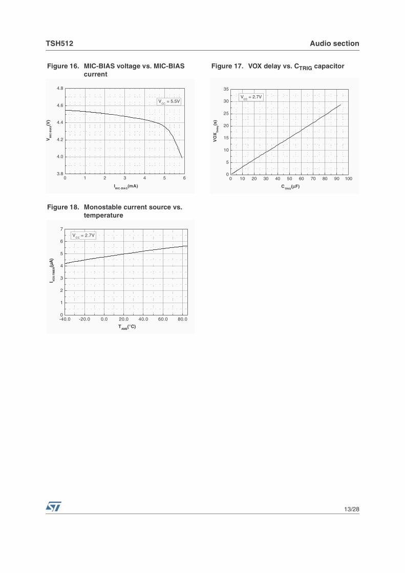
Figure 16. MIC-BIAS voltage vs. MIC-BIAS current
Figure 17. VOX delay vs. CTRIG capacitor
Figure 18. Monostable current source vs. temperature
0 1 2 3 4 5 63.8
4.0
4.2
4.4
4.6
4.8
VCC
= 5.5V
VM
IC-B
IAS(V
)
IMIC-BIAS
(mA)
0 10 20 30 40 50 60 70 80 90 1000
5
10
15
20
25
30
35
VCC
= 2.7V
VO
XD
elay
(s)
CTRIG
(µF)
-40.0 -20.0 0.0 20.0 40.0 60.0 80.00
1
2
3
4
5
6
7V
CC = 2.7V
I VOX
-TIM
ER(µ
A)
TAMB
(°C)

RF Section TSH512
14/28
6 RF Section
Figure 19. VCO output voltage vs. RVCO Figure 20. VCO-BIAS voltage vs. VCO-BIAS current
Figure 21. VCO & output buffer spectrum Figure 22. VCO-BIAS voltage vs. temperature
Figure 23. VCO & output buffer spectrum
10k 100k 1M300
350
400
450
500
550
600
650
700V
CC = 2.7V
L = 120µH (Q=30)F
CARRIER = 2.8MHz
VV
CO
-OU
T(m
VP
P)
RVCO
(Ω)
0 10 20 30 40 501.30
1.35
1.40
1.45
VCC
= 2.7VR
filter = 51Ω
Cfilter
= 470nF
VV
CO
-BIA
S(V
)IVCO-BIAS
(mA)
3 6 9 12 15 18-30
-20
-10
0
10
20
30
40
50
60
VCC
= 2.7VR
VCO = 22kΩ
ZL = 2kΩ
FCARRIER
= 2.8MHz
VB
UF
-OU
T(d
Bm
V)
Frequency(MHz)
-40 -30 -20 -10 0 10 20 30 40 50 60 70 801.3
1.4
1.5
1.6V
CC = 2.7V
No Load
VV
CO
-BIA
S(V
)
TAMB
(°C)
2.79
5
2.79
6
2.79
7
2.79
8
2.79
9
2.80
0
2.80
1
2.80
2
2.80
3
2.80
4
2.80
5
-30
-20
-10
0
10
20
30
40
50
60
VCC
= 2.7VL = 120µH (Q=30)R
VCO = no connected
ZL = 2kΩ
BW = 200HzF
CARRIER = 2.8MHz
VB
UF
-OU
T(d
Bm
V)
Frequency(MHz)

TSH512 Application Information
15/28
7 Application Information
This chapter gives application information for some typical applications.
7.1 Infrared stereo transmitter application (stereo headphones)
In this application, shown in Figure 24, the hi-fi stereo audio is amplified and level regulated by ALC. The carrier of each transmitter TX1 or TX2 of the TSH512 is modulated in FM and buffered to attack the LED final stage.
The audio signals are transmitted on the left and the right channels using a 2.8 & 2.3MHz carriers. The VOX activates the transmitter TX1 when the audio signal is present (see Figure 25).
Figure 24. Hi-fi stereo headphone block diagram
Audio
amp1
Audioamp2
SB
Y1
SB
Y2
²SQ
UE
LC
H
LNA
LNA + ALC
LNA + ALC
SBY
buffer1
buffer2
RX2
RX1
Line inputs
Rightchannel
Leftchannel
Vcc
LED
photodiode
filter
f ilter
2.3 MHz
2.8 MHz
Vcc: 2.3 to 5.5V
Current < 15 mA
TSH512 TSH511
20 mW / 16 Ω
20 mW / 16 Ω
Power supply:
2.3 to 5.5VIcc < 20 mA stereo
IR stereo HiFi transmitter Headphone side
HiFi stereo:
2.3 & 2.8 MHz carrie
rs
VOX
TX1
TX2
²SQ
UE
LC
HS
QU
ELC
H
RX2
RX1
LED
filter
20 mW / 16 Ω
20 mW / 16 Ω
:
:
VOX
TX1
TX2

Application Information TSH512
16/28
Figure 25. Application diagram
DE
C2
1
MIC
-BIA
S2
2
GN
D3
VC
C4
SB
Y5
VO
X-I
NT
S6
VO
X-S
EN
S7
VC
C8
GN
D9
MIC
-BIA
S1
10
DE
C1
11
LNA-INP112
LNA-INN113
LNA-OUT114
ALC-INT115
PEA-INN116
PEA-OUT117
VCO-BIAS118
VCC19
VCO-A120
VCO-B121
VCO-OUT122
GN
D23
BU
F-I
N1
24
BU
F-O
UT
125
VC
C26
VO
X-M
UT
E27
VO
X-I
NT
N28
VO
X-T
IME
R29
GN
D30
BU
F-O
UT
231
BU
F-I
N2
32
GN
D33
VCO-OUT234
VCO-B235
VCO-A236
VCC37
VCO-BIAS238
PEA-OUT239
PEA-INN240
ALC-INT241
LNA-OUT242
LNA-INN243
LNA-INP244
LN
A
+ -+ -
AL
C
PE
A
LN
A+-
+-
AL
C
PE
A
VO
X
+ -
Monosta
ble
IC2
TS
H512
R23
3K
9
C29
470nF
R24
470k
R32
10K
R31 47
C33
470pF
C42
2nF
2
C43
100nF
R36
270K
R35
100K
C35
470nF
C34
470nF
+5V
R26
47K C
36
56pF
C37
56pF
C45
6-60pF
C46
12pF
L2 120uH
R37
47K
+5V
C47
68pF
C38
56pF
C13
220nF
R21
33K
C28
470nF
+5V
C39
470nF
C30
1uF
R12
470K
R4
10K
R3
47
C6
470pF
C5
2nF
2
C8
100nF
R7
270K
R8
100K
C7
470nF
C18
470nF
+5V
R14
47KC
19
56pF
C20
56pF
C10
6-60pF
C11
12pF
R9
47K
+5V
C12
390pF
C21
56pF
C15
1uF
C14
470nF
+5V
C40
22nF
C24
22nF
D4
HS
DL4230
D6
HS
DL4230
Vcc
1 2 3
J2
JA
CK
3.5
ST
C32 1uF
C17
1uF
+5V
L1
120uH
C26
100uFV
cc
C44
39pFC9
39pF
R22
1K
8
R20
8K
2
R10
8K
2
R11
1K
8
C31
100nF
R25
47
C16
100nF
R13
47
R30 5K
6
C41
10uF
R2
5K6
C4
10uF
NC
0 O
hm
VO
X
ON
OF
F
R15
TX
1 =
2.8
MH
z
TX
2 =
2.3
MH
z
C23
100nF
C27
100nF
C22
10uF
R16
150K
R333K
R347K5
R6
3K
R5
7K5
D5
HS
DL4230
D7
HS
DL4230
D8
SMV1212
D3
SMV1212
Q1
ST
ZT
2222A
R19
10
R18
47
R17
2K
4
R27
2K
4
R28
24K
R29
2K
7
IC3
TS
H81
+5V
+5V
C25
100nF
R15
See N
ote
1812LS
(C
oilc
raft)
1812LS
(C
oilc
raft)
100m
W m
ini
(1206)
3 2
6
7
84
R38
1K
2
C48
22pF

TSH512 Application Information
17/28
7.2 Sub-carrier generator application: voice-operated wireless camera
Thanks to its operating frequency, the TSH512 offers the possibility of generating usual audio sub-carriers for video applications (Figure 26). The camera can be voice-activated using the VOX-MUTE output of the TSH512. The TSH512 also provides bias, amplification, ALC for the electret microphone.
Figure 26. Typical block diagram for audio sub-carrier generator
TSH512
LNA + ALC
LNA + ALC
MIC. BIAS
MIC. BIAS
TX2
VOX
SBY
buffer1
buffer2
Vcc
6 or 6.5 MHz filter
Electret CondenserMicrophone
Miniature camera
FM 2.4 GHztransmitter
6 or 6.5 MHzAudio sub-carrier
Video
VOX-MUTE
Stand-By
SSub-carrier
Stand-By
TX1
TSH512
LNA + ALC
LNA + ALC
MIC. BIAS
MIC. BIAS
TX2
VOX
SBY
buffer1
buffer2
Vcc
6 or 6.5 MHz filter
Electret CondenserMicrophone
Miniature camera
FM 2.4 GHztransmitter
6 or 6.5 MHzAudio sub-carrier
Video
VOX-MUTE
Stand-By
SSub-carrier
Stand-By
TX1

Application Information TSH512
18/28
7.3 Multimedia Application
7.3.1 Headset side
The TSH512 is used in mono to transmit the signal of the Electret Condenser Microphone of the headset. The circuit is supplied by batteries and the VOX function switches off the output stages to spare energy. The usual working frequency is 1.7MHz for infrared mono operation.
7.3.2 Computer side
In multimedia applications, the TSH512 transmits the hi-fi stereo from the PC to the headset.
Figure 27. Headset side block diagram
Figure 28. Computer side block diagram
TSH512
LNA + ALC
LNA + ALC
MIC. BIAS
MIC. BIAS
TX2
TX1
VOX
SBY
buffer1
buffer2
photodiode
Vcc
LED
Vcc
Audioamp2
SB
Y1
SB
Y2
LNA
2.3 MHz
Band-pass
TSH511
HiFi stereo from the PC:2 x 20 mW /16 Ω
1.7 MHz
Band-pass
Voice transmitted to the PC
Microphone Tx:
1.7 MHz
carrier
Stereo Rx:
2.3 & 2.8 MHz
f ilter
1.7 MHz
reject
2.8 MHz
Band-pass
TSH511 & 512 supply:2.3 to 5.5V, 25 mA
Audio
amp1
filter
f ilter f ilter
RX2
RX1
SQ
UE
LC
H
1.7 MHz
reject
f ilter
Vcc
-
HiFi
-
Microphone Tx:
1.7 MHz
carrier
Stereo Rx:
2.3 & 2.8 MHz
f ilter
-pass
:
f ilter
f ilter f ilter
SQ
UE
LC
H
f ilter
LNA + ALC
LNA + ALC
SBY
buffer1
buffer2
LED
photodiode
TSH511 & 512 supply:
2.3 to 5.5V, 24 mA
TSH512Audioamp1
Audio
amp2
SB
Y1
SB
Y2
SQ
UE
LC
HS
QU
ELC
H
LNA
RX2
RX1
filter
TSH511
Vcc1.7 MHz
Band-pass
HiFi stereo Tx:
2.3 & 2.8 MHz
mono Rx:
1.7 MHz
Voice from the headset microphoneHiFi stereo
VOX
TX2
TX1

TSH512 General Description
19/28
8 General Description
The TSH512 is a 0.4 to 11MHz dual FM analog transmitter. This circuit offers the functions needed for an advanced infrared STEREO transmitter. The access pins for each section allow a high versatility and therefore a lot of applications: mono infrared transmitter, stereo transmitter, mono/stereo sub-carrier generator for video transmissions (i.e.: popular 2.4GHz video links). The block diagram for the TSH512 is shown in Figure 1 on page 3.
Each audio input is amplified with a Low Noise Amplifier (LNA section) allowing connection to line level sources or directly to a microphone. Built-in voltage references ’MIC BIAS’ provide bias for Electret Condenser Microphones (ECM) with a high power supply rejection ratio.
Each audio path includes also an Automatic Level Control (ALC) to limit the over modulation and the distortion on very high signal amplitudes. The following operational amplifier (PEA) allows a pre-emphasis transfer function before modulating the varicap diode.
Built-in voltage references (VCO-BIAS) offers a regulated voltage to bias the varicap diodes. The Voltage Controlled Oscillator (VCO) is an integrated oscillator giving typically 600mV peak to peak at 2.8MHz.
The Output Buffer section linearly amplifies the FM carrier to provide a sinusoidal output. This sinusoidal signals reduce the inter-modulation products between the carriers, specially in two-way or in multi-carrier systems (see Application Information on page 15).
The Voice Operated Transmit (VOX) function automatically detects when an audio signal appear over the background noise.
The stand-by of the second transmitter reduces consumption in mono operation.
8.1 LNA section: low noise amplifier
For each transmitter, the audio source is connected to the LNA. The LNA stage is a low noise operational amplifier typically usable with a gain from 0dB to 40dB.
Figure 29. LNA schematic

General Description TSH512
20/28
The LNA gain is given by:
GLNA (dB) = 20.Log(1+RLNA2/RLNA1)
The High-pass cut-off frequency is:
fHPF = 1/(2.π.RLNA1.CLNA1)
The Lowpass filter cut-off frequency is:
fLPF = 1/(2.π.RLNA2.CLNA2)
If you connect an external circuit to the LNA output, the impedance of this external circuit should be higher than 10mΩ and the capacitance lower than 50pF in order to keep a good stability.
8.2 Electret condenser microphone source
When a Electret Condenser Microphone (ECM) is used, a high gain LNA is recommended, but low frequencies have to be attenuated. The ECM has to be biased with a stable and clean reference voltage.The TSH512 offers you the LNA and the MIC-BIAS sections to perform this functions (see Section 8.3. MIC-BIAS section: microphone bias voltage).
The capacitor C in series with the microphone stops the DC coming from MIC-BIAS.
The resistor R provides the DC from MIC-BIAS to supply the ECM.
Thanks to the ALC (Automatic Level control), the great variations of amplitude will not over-modulate the transmitter (refer to the chapter on ALC).
The self-adaptive VOX (Voice Operated Transmit) offers an automatic transmitting with a good discrimination of the background noise (see Section 8.5. VOX description: voice operated transmit).
Figure 30. Electret condenser microphone source

TSH512 General Description
21/28
8.3 MIC-BIAS section: microphone bias voltage
The MIC-BIAS bias voltages are dedicated to the bias of Electret Condenser Microphones. These bias voltages on pin 10 for TX1 and pin 2 for TX2, exhibit a low voltage noise density of 22nV/√Hz). This allows more than 55dB S/N considering a bandwidth of 7kHz (see Figure 30).
The MIC-BIAS voltage is related with VCC as follow (with I MIC-BIAS= 2.5mA):
VMIC-BIAS = 0.844.Vcc-0.140 (Volts)
Moreover, the supply rejection ratio is guaranteed to be better than 50dB without any decoupling capacitor. To address biasing of most of the microphones, the current drive capability is 2.5mA. The MIC-BIAS voltage depends linearly on the supply voltage VCC (refer to Figure 11).
8.4 ALC section: automatic level control
Both transmitters of the TSH512 include Automatic Level Control (ALC). When the level of the audio signal is too high, the ALC compresses the signal in order to avoid over-modulation of the FM VCO. In this way, the ALC reduces the distortion and maintains a reduced transmit spectrum with very high-amplitude signals.
The ALC features a 20dB gain and an output signal regulated to 700 mVpp in compression.
The attack time is the response time of the ALC to go from the linear amplification to the compression region. The attack time mainly depends on CALC capacitor value. A typical value of CALC is 1µF with music as the audio signal (refer to Figure 25).
The decay time is the response time the ALC requires to recover to full gain amplifying mode after being in compression mode. The decay time depends mainly on the RALC resistor value. A typical value of RALC is 470kΩ, with music as audio signal (refer to Figure 25).
Figure 31. Automatic level control schematic

General Description TSH512
22/28
8.5 VOX description: voice operated transmit
The Voice Operated Transmit section (VOX) reduces consumption when there is no audio signal to transmit. When the VOX detects that no audio signal is present, it mutes the Output Buffers of TX1 and TX2 and provides the logic signal VOX-MUTE to switch-off external LED drivers if needed.
The audio signal of TX1 is amplified with a gain dependent on the values of Rsens and Csens. Rsens and Csens are connected to pin 7. The high-pass filtering has the following cut-off frequency:
On pin 6, Rpeak and Cpeak integrate the rectified audio signal with a short time constant. This filtered signal follows the audio amplitude.
Figure 32. VOX delay and sensitivity schematic
HPFf 1
2π Rsens Csens⋅( )-----------------------------------------------------=

TSH512 General Description
23/28
The self-adaptive VOX threshold is necessary because the ambient background noise variation is slow compared to the voice or the music. On the pin 28, RCOMP and CCOMP integrates the amplitude to follow the background amplitude. Therefore, the comparator switches when an audio signal appears over the background noise. Referring to Figure 2, CCOMP will be typically a 100nF capacitor and RCOMP will be determined depending on the audio signal.
As soon as an audio signal is detected, the output of the monostable switches to ’high’ state and enables both output buffers. The output of the monostable is the pin 27 and is called ’VOX-MUTE’.
The monostable holds the TSH512 in transmit mode during a delay fixed by the value of CTRIG connected to pin 29.
Please note that the VOX function is activated when the audio signal enters the first transmitter TX1.
When the application needs a permanent transmission, it is possible to inhibit the VOX function. Just remove the CTRIG capacitor and connect pin 29 to ground.
As soon as the TSH512 is powered-on, the internal reset circuitry sets the VOX-MUTE to high state to enable transmission. The transmission remains during the monostable timing and continues if an audio signal triggers the monostable.
Figure 33. VOX integrator and monostable schematic
VOXDELAY1.4V5µA------------⎝ ⎠⎛ ⎞ Ctrig⋅=

General Description TSH512
24/28
8.6 PEA section: pre-emphasis
The amplitude-regulated audio coming from the ALC feeds the positive input of the operational amplifier called PEA (Pre-Emphasis). The pre-emphasis consists in a high-pass filter in order to compensate the behavior of the FM transmission.
RPEA1 and CPEA1 set the time constant of the pre-emphasis as:
τ = RPEA1. CPEA1
50 µs or 75µs time constants are generally used.
Choosing the gain of the PEA stage also allows one to set the right modulation level to the varicap diode. The gain in the pass-band is:
GPEA = 1+ (RPEA2/RPEA1)
Figure 34. VOX state at power-on
Figure 35. Pre-emphasis schematic
time
VOX -MUTE
POWER SUPPLY
on
off
VOX Delay(Ctrig)
0
1high state if retriggered by audio

TSH512 General Description
25/28
8.7 VCO section: voltage controlled oscillator
Each TSH512 transmitter has its own oscillator to generate the carrier. The audio signal is applied to the varicap diode to perform the Frequency Modulation. Thanks to the VCO-BIAS voltage reference, the DC bias of the varicap is stabilized. The high PSRR (Power Supply Rejection ratio) of the VCO-BIAS ensures good immunity with the noise of the power supply.
The generated frequency can be set from 400 kHz to 11 MHz by external components. Refer to the table 1 for the usual frequencies in Infrared audio.
The working frequency is:
where Ct is the total capacity of CL, Cp, Cs and Cv:
Ct = 1/(1/Cc+1/CL) with Cc = Cp+1/(1/Cv+1/Cs)
It’s possible to use varicap diodes SMV1212 (Alpha Ind.) or ZC833 (Zetex).
The output level of the VCO can be reduced by adding the resistor RVCO between pin 19 and pin 20 or between pin 36 and pin 37 for TX1 and TX2 respectively.
Figure 36. VCO schematic
Table 5. Usual Infrared frequencies
IR frequency in MHz Applications
1.6 AM mono
1.7 FM mono
2.3 FM right channel
2.8 FM left channel or mono
VCOf 1
2π L Ct⋅( )------------------------------=

General Description TSH512
26/28
8.8 Output buffer section
The output buffers are able to deliver a sinusoidal signal with 1.5Vpp amplitude in a 1kΩ load. This impedance is compatible with popular biasing circuitry of external transistor drivers of IR LEDs.
The VOX-MUTE logic signal can be used to control the external LED drivers. When the audio is not present on the TX1 input, VOX-MUTE is at ’Low’ state, the TSH512’s internal buffers are muted, and external drivers can be switched off by controlling their bias.
8.9 SBY pin: standby for mono operation
A high state on the Standby pin (SBY) sets the second transmitter TX2 in power-down. The SBY pin is typically used when the TSH512 is used as a mono transmitter (i.e. infrared microphone transmitter).
TSH512 Package Mechanical Data
27/28
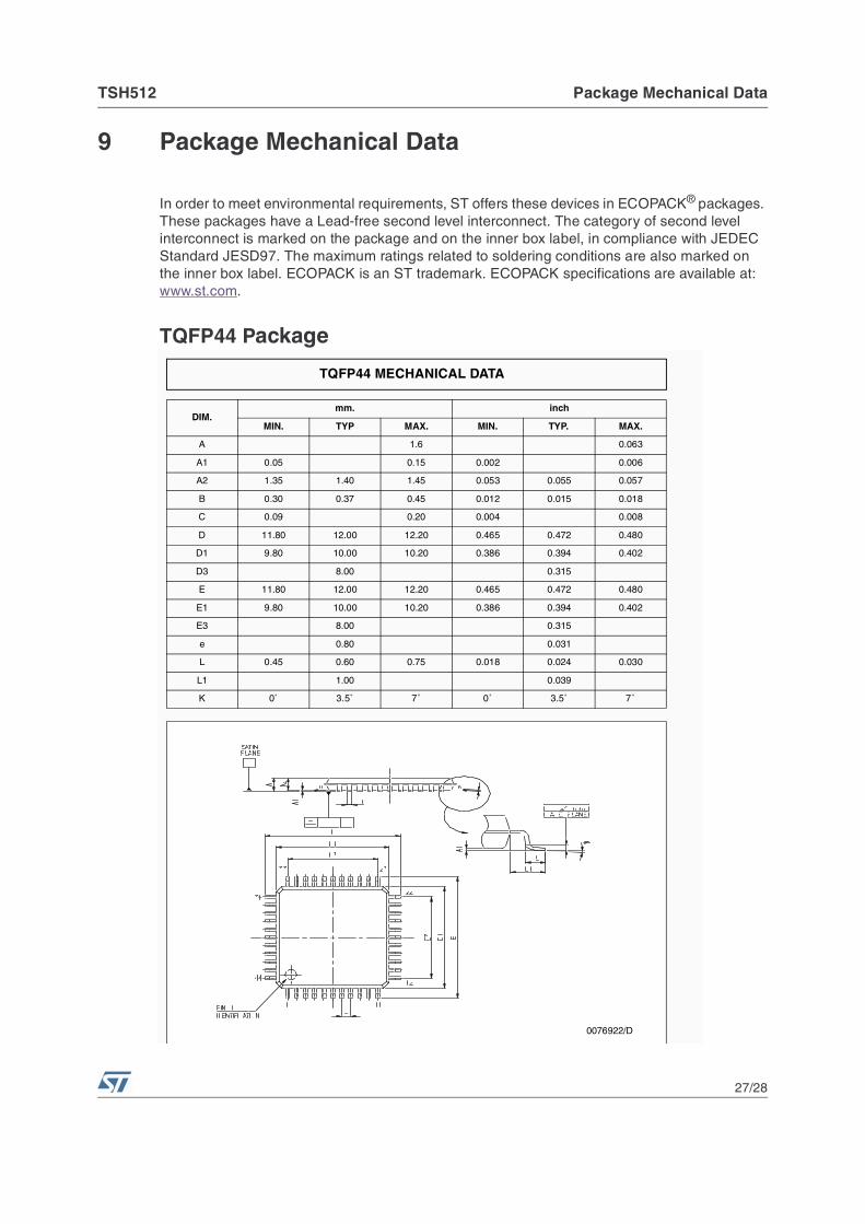
9 Package Mechanical Data
In order to meet environmental requirements, ST offers these devices in ECOPACK® packages. These packages have a Lead-free second level interconnect. The category of second level interconnect is marked on the package and on the inner box label, in compliance with JEDEC Standard JESD97. The maximum ratings related to soldering conditions are also marked on the inner box label. ECOPACK is an ST trademark. ECOPACK specifications are available at: www.st.com.
TQFP44 Package
DIM.mm. inch
MIN. TYP MAX. MIN. TYP. MAX.
A 1.6 0.063
A1 0.05 0.15 0.002 0.006
A2 1.35 1.40 1.45 0.053 0.055 0.057
B 0.30 0.37 0.45 0.012 0.015 0.018
C 0.09 0.20 0.004 0.008
D 11.80 12.00 12.20 0.465 0.472 0.480
D1 9.80 10.00 10.20 0.386 0.394 0.402
D3 8.00 0.315
E 11.80 12.00 12.20 0.465 0.472 0.480
E1 9.80 10.00 10.20 0.386 0.394 0.402
E3 8.00 0.315
e 0.80 0.031
L 0.45 0.60 0.75 0.018 0.024 0.030
L1 1.00 0.039
K 0˚ 3.5˚ 7˚ 0˚ 3.5˚ 7˚
TQFP44 MECHANICAL DATA
0076922/D

Revision History TSH512
28/28
10 Revision History
Date Revision Changes
Aug. 2001 1 First release corresponding to Preliminary Data version of datasheet.
Sept. 2001 2
Datasheet updated for Maturity 30:
– ESD sensitive device sentence added
– 4 curves updated
– Electrical parameters updated
Dec. 2003 3
Specific content changes as follows:
– Application diagrams updated
– Releases on curves
– Application schematic diagram update
– Electrical parameters updated
Dec. 2003 3
Specific content changes as follows:
– Application diagrams updated
– Releases on curves
– Application schematic diagram update
– Electrical parameters updated
Oct. 2005 5– PPAP reference inserted in the datasheet see Table . Order Codes
on page 1.
Information furnished is believed to be accurate and reliable. However, STMicroelectronics assumes no responsibility for the consequencesof use of such information nor for any infringement of patents or other rights of third parties which may result from its use. No license isgranted by implication or otherwise under any patent or patent rights of STMicroelectronics. Specifications mentioned in this publication aresubject to change without notice. This publication supersedes and replaces all information previously supplied. STMicroelectronics productsare not authorized for use as critical components in life support devices or systems without express written approval of STMicroelectronics.
The ST logo is a registered trademark of STMicroelectronics.All other names are the property of their respective owners
© 2005 STMicroelectronics - All rights reserved
STMicroelectronics group of companies
Australia - Belgium - Brazil - Canada - China - Czech Republic - Finland - France - Germany - Hong Kong - India - Israel - Italy - Japan - Malaysia - Malta - Morocco - Singapore - Spain - Sweden - Switzerland - United Kingdom - United States of America
www.st.com