Heterojunctions Heterostructures Quantum confined structures
43
Heterojunctions Heterostructures Quantum confined structures
Transcript of Heterojunctions Heterostructures Quantum confined structures

Heterojunctions
Heterostructures
Quantum confined structures

HETEROJUNCTIONS & HETEROSTRUCTURES
HETEROJUNCTION is the interface between two layers or regions of different
semiconductors, in other words two semiconductors with different crystal structure or
different crystal phase. Semiconductors of different materials or of the same material but
different crystal phase have different band gaps as opposed to a homojunction.
HETEROSTRUCTURE is the combination of multiple heterojunctions. The requirement that
each material be a semiconductor with unequal band gaps is somewhat loose, especially
on small length scales, where electronic properties depend on spatial properties. A more
modern definition of heterojunction is the interface between any two solid-state
materials, including crystalline and amorphous structures of metallic, insulating, fast ion
conductor and semiconducting materials.

Energy Band Alignment
The behaviour of a semiconductor junction depends on the alignment of the bands
at the interface. Semiconductor interfaces can be organized into three types of
heterojunctions:
Straddled – Type I Staggered – Type II Broken – Type III
Heterojunction Basics
• Band offsets for common III-V heterojunctions
• Note: broken gap occurs for III-V pairs when both group III and V elements differs • Alternate layers will have
excess charge carriers in all layers without doping
• Electrons from GaSb valence band will fill into InAs conduction band…
• Semimetal

bangap engineering
Optical properties of the materials
Change energy levels and states Change of density of states
Change of electronic properties
QUANTUM CONFINEMENT & QUANTUM CONFINED STRUCTURES
If one makes a heterostructure with sufficiently thin layers, quantum interference effects
begin to appear prominently in the motion of the electrons.
The resulting structure is then called a low-dimensional structure or system:
Nanostructures
The confinement of particles, usually electrons or holes, to a low- dimensional structure
leads to a dramatic change in their behaviour and to the manifestation of size effects that
usually fall into the category of quantum-size effects.
Therefore low dimensional structures or materials are also known as Quantum Confined
Structures exhibit new physicochemical properties not shown by the corresponding large-
scale structures of the same composition. Suitable control of the properties and
responses of nanostructures can lead to new devices and technologies.

Quantum effects: The quantum confinement is observed when the diameter of the particle is of the same magnitude as the wavelength of the electron (wave function). Quantum confinement is responsible for the increase of energy difference between energy states and band gaps, which relates to the optical and electronic properties of the materials. Therefore, when materials are these small, their electronic and optical properties deviate substantially from those of bulk materials (example is gold).
For nanoparticles the size of the
particle imposes geometrical
constraints on the electrons, which
respond by adjusting their energy.
This phenomenon is called the
quantum size effect.
(Recalling Lecture 13)

Excitons
An exciton can form when a material absorbs a photon of higher energy than its bandgap. This excites an electron from the valence band into the conduction band creating and electron-hole pair. The electron in the conduction band is then attracted to the hole by the Coulomb forces generated between the electrons surrounding the hole and the excited electron.
Excitons, on the other hand, determine the band-to-band transition the optical properties around the band gap,i.e., in the visible including the near UV and IR in the case of semiconductors and in the (V)UV for insulators.
It is an electrically neutral quasiparticle that exists conceptually in insulators, semiconductors and some liquids.
The exciton is regarded as an elementary excitation of condensed matter that can travel through a crystal structure and transport energy without transporting net electric charge.

Excitons can be treated as “Bohr atoms”
Re.
mmREE *
h*e
81112
2
2
220
επ∆∆ −
++=
Electronic energy gap:
*2
204
mer
πεε=
When the size of the nanoparticle approaches that of an exciton, size quantization occurs.
Intrinsic band gap
NP radius electrostatic correction

Exciton Bohr Diameter

The quantum effects of confinement become significant when at least one of the dimensions of a structure is comparable in length to the de Broglie wavelength. If at least one dimension of a solid is comparable to the de Broglie wavelength of the particle, a quantum-mechanical treatment of particle motion becomes necessary.

Classification of Low-dimensional Structures/Materials Low-dimensional structures are usually classified according to the number of reduced dimensions they have. More precisely, the dimensionality refers to the number of degrees of freedom in the particle momentum: o Three-dimensional (3D) structure or bulk structure: No quantization of the
particle motion occurs, i.e., the particle is free.
o Two-dimensional (2D) structure or quantum well: Quantization of the particle motion occurs in one direction, while the particle is free to move in the other two directions.
o One-dimensional (1D) structure or quantum wire: Quantization occurs in two directions, leading to free movement along only one direction.
o Zero-dimensional (0D) structure or quantum dot (sometimes called “quantum
box”): Quantization occurs in all three directions.

Quantum-Confined Structures… ….When the motion of the electrons (and/or holes) is confined in one or more directions by potential barriers. The general scheme for classifying quantum-confined structures is given in the following table. Quantum size effects become important when the dimensions of the structure become comparable with the de Broglie wavelength of the electrons or holes, leading to energy levels called "energy sub-bands", i.e., the carriers can only have discrete energy values. If we consider the free thermal motion of a particle of mass m in the z-direction, the de Broglie wavelength at a temperature T is approximately given by,


The quantization of the motion in the z-direction has three main consequences: 1. the quantization energy shifts the effective band edge to higher energy, which provides
an extra degree of freedom in the art of bandgap engineering.
2. the confinement keeps the electrons and holes closer together and hence increases the radiative recombination probability.
3. the density of states becomes independent of energy, in contrast to 3-D materials, where the density of states is proportional to E1∕2.
In zero dimensions the energy states are sharp levels corresponding to the eigenstates of the system.
Many of the useful properties of the QWs follow from these three properties.

QUANTUM WELLS are potential wells with only discrete energy values. The term “well” refers to a semiconductor region that is grown to possess a lower energy, so that it acts as a trap for electrons and holes (electrons and holes gravitate towards their lowest possible energy positions). Quantum wells are real-world implementation of the “particle in the box” problem; they act as potential wells for charge carriers and are typically experimentally realized by epitaxial growth of a sequence of ultrathin layers consisting of semiconducting materials of varying composition.

Confinement in 2d nanostructures
3D systems
2D systems
B A B
( )2
2 2( ) , 1,2,3...2
nn x y zE k k k E n
µ= + + =
B A B
AgE
BgE
k
( )nE k
E

Quantum well (QW)
width L, infinite barriers
= x
Ln
Lx πψ sin2)(
0)()0( == Lψψ
E
222
2
2
28
==
Ln
mn
mLhEn
π
parabolic dependence
22
2k
m
=
Lnk π
=
2D: electrons are bound along x, free to move perpendicularly

Two different semiconductors with different band gaps can be joined to form a heterojunction. The discontinuity in either the conduction or the valence band can be used to form a potential well. If 1 thin layer of a narrower-band gap material A is sandwiched between 2 layers of a wider-band gap material B, then they form a double heterojunction. If layer 'A' is sufficiently thin for quantum properties to be exhibited, then such a band alignment is called a single quantum well. Type of manipulations
• Additional semiconductor layers can be included in the heterostructure, for example a
stepped or asymmetric quantum well can be formed by the inclusion of an alloy between materials A and B.
• QWs can be grown as strained layers on top of a lattice with a different unit cell size. (typical example:In x Ga1−xN/GaN). These layers do not satisfy the lattice-matching condition, but as long as the total In x Ga1−xN thickness is less than the critical value, there is an energy barrier to the formation of dislocations - Strained Quantum Wells.
In practice, this allows considerable extra flexibility in the bandgap engineering that can be achieved.

Still more complex structures can be formed, such as symmetric or asymmetric double quantum well and multiple quantum wells or superlattices. The difference between the latter is the extent of the interaction between the quantum wells; a multiple quantum well exhibits the properties of a collection of isolated single quantum wells, whereas in a superlattice the quantum wells do interact.
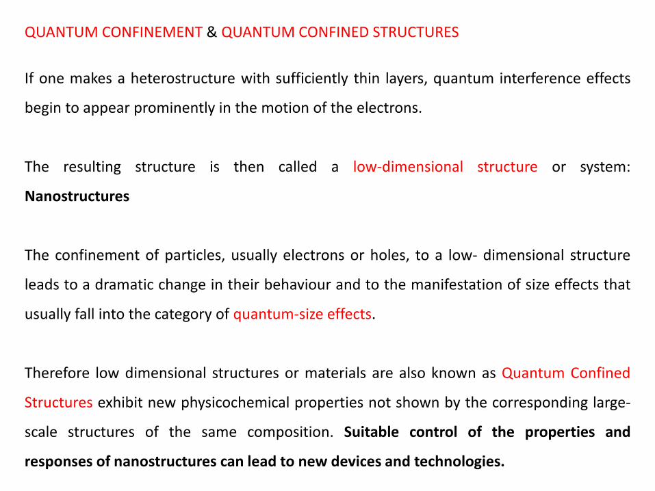
(a) Schematic diagram of an AlAs/GaAs quantum well. The electrons are confined along z (showing the three lowest energy confined eigenstates) and free to move in the x-y plane. (b) A quantum wire is formed at the intersection of the T-shaped (shaded) region formed by two 10 nm GaAs type I quantum wells, confined by Alx Ga1 − x As barriers. (c) Application of gates on a 2D electron gas (2DEG) to confine electrons into a lateral quantum dot, typically of size of a few tens of nanometer. Ref.: https://www.sciencedirect.com/topics/physics-and-astronomy/quantum-wells
quantum well quantum wire quantum dot

Assembly process where smaller particles join to make a larger structure.
Building things at the Nanoscale
Top-down approach Bottom-up approach Process that starts by a bulk amount of the material we plan to use for nanowires and carve it away down to the right size.
More details on the techniques can be found in powerpoint L15-NanoSynthesis, that will be placed online together with this lectures.

QUANTUM WIRE A quantum well layer can be patterned* to leave a free standing strip of quantum well material; the electron (or hole) is now free to move in only one direction. Any charge carriers are still confined along the heterostructure growth (z-) axis, as they were in the quantum well, but in addition (provided the strip is narrow enough) they are now confined along an additional direction, either the x- or the y-axis, depending on the lithography.
*By Photolithography or electron-beam lithography, and etched.

“Pseudowires”
Lithography and etching
Formation of 2d quantum well
Coating with resist
Create pattern
Etch, until wire remains
Disadvantages: optical and electrical dead layer because of defects due to etching
Sometimes overgrown again to shield wire!

Growing Nanowires

Nanowire superlattice
Upon completion of the first growth step, a different material (red) can be grown from the end of the nanowire. Repetition of steps leads to a compositional superlattice within a single nanowire.

Diameter (d) of NWs range from 1 nm – 100 nm. Length (ℓ) varies from 10 nm – 1 µm
– Nanowires: wires with large aspect ratios (ℓ/d > 20) – Nanorods: wires with small aspect ratios (ℓ/d) – Nanotubes: hollow wires
Vorführender
Präsentationsnotizen
Germanium nanowires (GeNWs) have attracted much attention in recent years[1-9] owing to the advanced electrical properties of Ge such as high carrier mobilities[10] and the ability of facile chemical synthesis of single crystal GeNWs at low temperatures well below 400 °C[5].

Summary of single crystal nanowires synthesized

Applications - Nanowire heterostructures
+ axial heterostructures, e.g. GaP-GaAs heterojunction
+ radial heterostructures, e.g. Si-Ge
+ Nanowire superlattices

Björk et al., NanoLetters 2, 87 (2002)
InAs InP InAs
• Almost atomically sharp interfaces • No strain-induced dislocations (stress can relax at the surface)
Heterostructures nanowires
(Samuelson’s group – Lund)

QUANTUM DOTS Quantum dots can again be formed by further patterning (lithography and etching) to leave pillars rather than wires, then a charge carrier can become confined in all three dimensions.


Some examples of QD Heterostructures
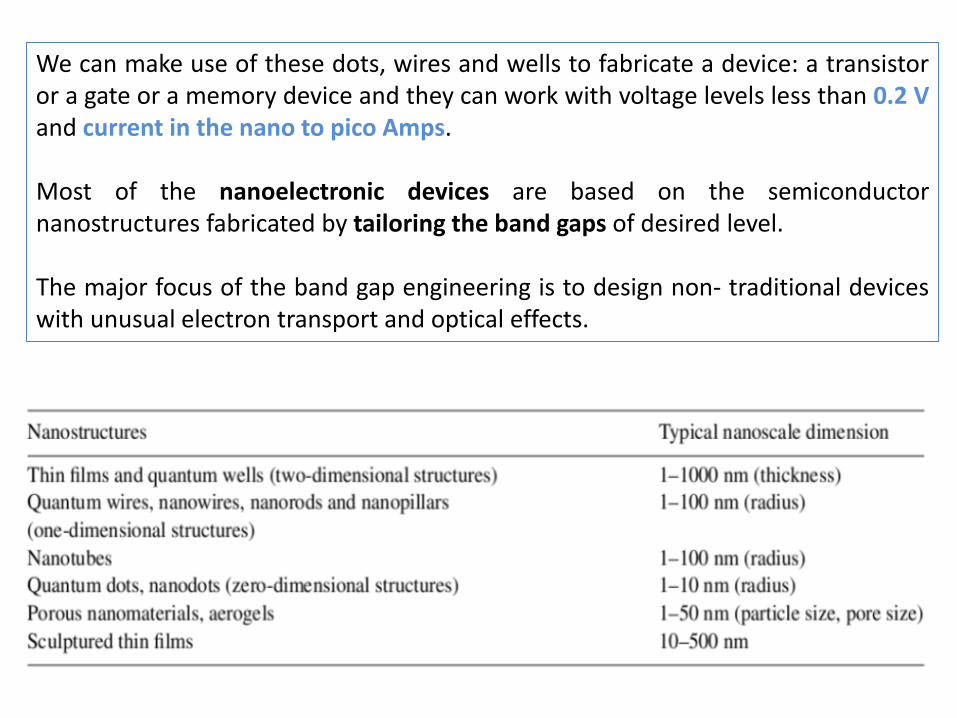
We can make use of these dots, wires and wells to fabricate a device: a transistor or a gate or a memory device and they can work with voltage levels less than 0.2 V and current in the nano to pico Amps. Most of the nanoelectronic devices are based on the semiconductor nanostructures fabricated by tailoring the band gaps of desired level. The major focus of the band gap engineering is to design non- traditional devices with unusual electron transport and optical effects.

Next Lecture
Quantum confinement in more detail
Understanding the QC effects with exercises