Heterointerfaces in Semiconductor Nanowires
22
Nanowire heterointerfaces DOI: 10.1002/smll.200800556 Heterointerfaces in Semiconductor Nanowires Ritesh Agarwal* reviews R. Agarwal Examples of advanced nanowire heterostructures and their characterization. From the Contents 1. Introduction . . . 1873 2. Heterostructure NW Synthesis, Characterization, and Assembly . 1874 3. Semiconductor-NW– Metal-Contact Interfacial Properties .... 1875 4. NW–Dielectric Interfacial Properties .... 1878 5. Crossed-NW Devices ...... 1881 6. NW–Substrate Interface for Functional Devices ...... 1883 7. Axial Heterostructures 1884 8. Radial Heterostructures 1888 9. Conclusions . . . 1890 Keywords: electronics heterostructures interfaces nanowires photonics 1872 ß 2008 Wiley-VCH Verlag GmbH & Co. KGaA, Weinheim small 2008, 4, No. 11, 1872–1893
-
Upload
ritesh-agarwal -
Category
Documents
-
view
227 -
download
2
Transcript of Heterointerfaces in Semiconductor Nanowires

reviews R. Agarwal
1872
Nanowire heterointerfaces
DOI: 10.1002/smll.200800556
Heterointerfaces in Semiconductor NanowiresRitesh Agarwal*
Examples of advanced nanowire heterostructures and their characterization.
From the Contents
1. Introduction . . . 1873
2. Heterostructure
NW Synthesis,
Characterization,
and Assembly . 1874
3. Semiconductor-NW–
Metal-Contact
Interfacial
Properties . . . . 1875
4. NW–Dielectric
Interfacial
Properties . . . . 1878
5. Crossed-NW
Devices . . . . . . 1881
6. NW–Substrate
Interface for
Functional
Devices . . . . . . 1883
7. Axial
Heterostructures1884
8. Radial
Heterostructures1888
9. Conclusions . . . 1890
Keywords:� electronics
� heterostructures
� interfaces
� nanowires
� photonics
� 2008 Wiley-VCH Verlag GmbH & Co. KGaA, Weinheim small 2008, 4, No. 11, 1872–1893

Heterointerfaces in Semiconductor Nanowires
Semiconductor nanowires have attracted considerable recent interest due to
their unique properties, including their highly anisotropic geometry, large
surface-to-volume ratio, and carrier and photon confinement. Currently,
tremendous efforts are devoted to the rational synthesis of advanced
nanowire heterostructures. Yet, if functional devices are to be made from
these materials, precise control over their composition, structure,
morphology, and dopant concentration must be achieved. Their funda-
mental properties must also be carefully investigated since the presence of a
large surface and interfacial area in nanowires can profoundly alter their
performance. In this article, the progress, promise, and challenges in the area
of nanowire heterostructured materials are reviewed, with particular
emphasis on the effect of different types of heterointerfaces on device
properties.
1. Introduction
The aggressive scaling down of devices to sub-100-nm
length scales remains the cornerstone for creating integrated
systems with enhanced functionality. The highly prolific
microelectronic industry has successfully utilized the top-
down approach for such device scaling,[1] which involves using
photolithographic and subsequent etching techniques to
reduce the device size, and has tremendously impacted almost
all aspects of our lives. However, it is becoming increasingly
difficult to continue this scaling trend due to the fundamental
limitations of photolithography, which uses tightly focused
optical radiation to transfer the electronic device design on a
planar substrate. This limitation comes from the classical
optical phenomena of diffraction, which limits the size of the
optical beam that can be focused on to small spot size, making
the goal of fabricating devices with arbitrarily small feature
sizes rather difficult. Possible approaches to reduce the critical
size of devices includes the use of smaller-wavelength
radiation (extreme-UV), higher-numerical-aperture lenses,
and aggressive etching; all of these are promising to continue
the scaling trends in the semiconductor industry but involve
prohibitively expensive procedures that may not be able to
maintain the lower costs of electronic devices that have
become essential commodities in the modern world.
One promising approach to overcome the fundamental
challenges inherent with the top-down fabrication method is
the bottom-up self-assembly technique, which mostly utilizes
chemical techniques for arranging and manipulating matter at
the atomic scale with exquisite control over the spatial
arrangement of atoms to form novel structures. The bottom-
up self-assembly technique is a unique approach for device
[�] Prof. R. Agarwal
Department of Materials Science and Engineering
University of Pennsylvania
Philadelphia, PA 19104 (USA)
E-mail: [email protected]
small 2008, 4, No. 11, 1872–1893 � 2008 Wiley-VCH Verlag Gmb
fabrication as the functionally of the device originates during
the growth of the structures and not from lithography, thereby
enabling functional structures that can be arbitrarily small
ranging from small molecules to mesoscopic structures such as
nanocrystals, nanotubes (NTs), and nanowires (NWs) in the
sub-100-nm length scale.[2] Impressive progress has beenmade
in the past decade in the area of nanostructured materials and
it is becoming increasingly clear that such non-traditional
approaches for assembling devices will be critical for achieving
the predicted metrics of next-generation computing, as well as
opening new opportunities across different scientific disci-
plines[2,3] by providing a methodology for scaling of devices to
the molecular scale with minimal surface roughness. Since the
bottom-up approach presents a new paradigm for assembling
functional devices, it also provides new challenges that need to
be overcome in order to make it a viable option for future
technologies. These challenges include generatingmethods for
rational synthesis of nanostructures with controlled properties
with minimum dispersion, understanding the novel physical
phenomena in quantum- or finite-sized structures, their
integration into devices, and finally the most challenging
requirement of developing new large-scale assembly tech-
niques for arranging these nanostructures into hierarchically
ordered and fully functional structures. Only when these
challenges are overcome would the bottom-up technology be
able to address interesting problems related to electronics,
photonics, information technology, medicine, sensors, and
diagnostics. This scheme for growing nanoscale components
and then assembling devices from the ‘‘bottom up’’ is also very
promising to overcome amajor obstacle faced by conventional
planar technology, where the ‘‘top down’’ nature of the
fabrication process imposes tremendous constraints on the
integration of vastly different materials. For example, even a
modest goal of integrating electronics and photonics on a
single chip is difficult in top-down processes owing to the
incompatibility of direct-bandgap semiconductors with Si.
However, since the nanoscale components can be synthesized
and then co-assembled on a common platform in separate
H & Co. KGaA, Weinheim www.small-journal.com 1873

reviews R. Agarwal
Ritesh Agarwal earned his under-
graduate degree from the Indian
Institute of Technology, Kanpur in
1996, and a master’s degree in
chemistry from the University of
Chicago in 1997. He received his PhD in
physical chemistry from the University
of California at Berkeley in 2001. After
completing his PhD, he was a post-
doctoral fellow at Harvard where he
studied the optical and photonic
properties of semiconductor nano-
wires. His work led to the development
of electrically driven single-nanowire
lasers and avalanche photodiodes. He is currently an assistant
professor in the Department of Materials Science and Engineering
at the University of Pennsylvania. His research interests include
size-dependent structural, optical, and electronic properties,
quantum-confined optics in nanowire heterostructures, and
studying phase transitions and electronic memory switching at the
nanoscale.
1874
processes, it opens up exciting opportunities to create complex
systems with multifunctional components with electronic,
optical, and magnetic properties.
Semiconductor NWs and NTs offer a versatile approach
for the bottom-up assembly of electronic and photonic devices
with the potential for integration of non-silicon-based
photonics with silicon electronics.[3–13] The unique geometries
of NWs and NTs enable them to function as both active device
elements and interconnects, which can be utilized to achieve
highly integrated device architectures. The inability to control
the chirality and hence the electronic properties of nanotubes
during synthesis and the difficulties associated with manip-
ulating individual NTs presents a significant challenge in
developing NT-based integrated devices. By contrast, the
ability to rationally synthesize NWs with tunable and
modulated chemical composition, size, structure, and mor-
phology and to accurately dope them with both p- and n-type
dopants has opened up opportunities for assembling almost
any kind of functional nanosystem ranging from photonics and
electronics to biological sensors.
One defining attribute of nanostructured devices is the
presence and significance of interfaces, which becomes
particularly important at sub-100-nm size scales. The role of
interfaces and interfacial states becomes all the more
important for NW heterostructures with electrical contacts.
An example of different types of interfaces in a typical core/
shell heterostructured NW transistor device is shown in
Figure 1. The different interfaces include the heterointerface
between the two semiconducting materials (e.g., Si and Ge),
semiconductor–gate-oxide interface, semiconductor–metal
contact interface, and semiconductor–vacuum interface, which
are in intimate contact with the NW, in addition to the gate-
oxide–gate-electrode interface not in direct contact with the
NW. The unique interplay of the properties of all these
interfaces has a profound effect in determining the properties
of the functioning NW device. For example, the size-
dependent band-edge alignments between the two semicon-
ductors, nature of the interface, crystallinity, doping levels,
defects, and other properties determine the unique properties
of just this one heterojunction interface! Similarly, the metal–
Figure 1. A schematic image of a core/shell nanowire transistor device
assembled on a dielectric substrate indicating the different hetero
interfaces. The interfaces include semiconductor-NW–bottom-substrate
interface, semiconductor-NW–metal contacts, core/shell interface
between different semiconductors, NW–gate-dielectric interface
(conformal or deposited on top), and a nondirect contact interface
between dielectric and gate metal.
www.small-journal.com � 2008 Wiley-VCH Verlag Gm
semiconductor contact will be influenced by the metal work
function, semiconductor-electron affinity or ionization poten-
tial, and also critically on the nature of surface states that can
lead to the pinning of the Fermi level at the contact region,
rendering contact properties independent of the type of metal
used. In this article, we will review the significant progress
made in the field of semiconductor NW devices, with emphasis
on the unique properties that emerge due to the presence of
heterojunctions and interfaces in different geometries and
their effect on the device properties.
2. Heterostructure NW Synthesis, Characterization,and Assembly
Semiconductor NWs are typically synthesized by the
vapor–liquid–solid (VLS) growthmechanism, in which ametal
nanoparticle functions as a catalyst for one-dimensional (1D),
anisotropic growth.[5,10,14–16] The gas-phase reactants mix with
the catalyst, which is kept at elevated temperatures to form a
supersaturated melt, at which point the reactants precipitate
via nucleation, and subsequent axial elongation of a crystalline
NW occurs. Single-crystalline NWs can be synthesized with
excellent control over diameter, chemical composition, and
dopant concentration from practically any semiconducting
material with diameters ranging from a few nanometers to
200 nm and with typical aspect ratios of 100–1000.
Manipulation of matter at the nanoscale should lead to
fascinating and novel behavior and should also impact device
properties. In analogy to planar semiconductor technology
where impressive advances have been made towards control-
ling heterostructures for various applications,[17] NW hetero-
structures hold tremendous promise for nanoelectronics and
photonics applications.[10] The ability to fabricate intrawire
heterostructures with well-defined crystalline interfaces
bH & Co. KGaA, Weinheim small 2008, 4, No. 11, 1872–1893

Heterointerfaces in Semiconductor Nanowires
should greatly increase the versatility of NW-based photonic
devices and also reduce the load for subsequent assembly
processes with increased functionality within NWs.[18] Such a
synthetic control will be extremely useful for creating precisely
defined systems to investigate the effects of confinement on
properties of nanostructures resulting from themodification of
the electronic structure and density of states.
The unique geometry of NWs allows three types of
structurally coherent, epitaxially grown heterostructures:
1) axial, 2) radial (core/shell), and 3) branched heterostruc-
tures[19–22] (Figure 2). To synthesize axial heterostructures, the
addition of the first reactant is stopped during growth and a
second reactant is introduced, which grows along the NW axis.
To grow radial heterostructures, the VLS growth is minimized
and the second reactant grows epitaxially on the NW core.
Branched heterostructures are typically synthesized by
depositing the metal nanocatalysts after the growth of NW
backbones, which then can seed the growth of higher-
generation branches, preferably epitaxially from the first-
generation NWs. In addition to the epitaxially grown NW
heterostructures, it is also possible to fabricate functional
heterojunctions between two crossed NWs and also between
NWs assembled on a clean semiconductor substrate, both
formed due to van der Waals or other physical interactions.
Assembly of crossed-NW junctions can be reliably formed by
microfluidic-based flow,[25] electric field,[26] optical twee-
zers,[27] or Langmuir–Blodgett-based[28] alignment tech-
niques. The heterojunction formed between two crossed
NWs is unique because of the extremely small area of contact,
its ease of fabrication, and the ability to combine different
Figure 2. Nanowire heterostructures. An illustration of NW axial,
branched, and radial heterostructure growth schemes. Transmission
electron microscopy (TEM) images of InAs/InP axial [23] and Si/Ge
radial [24] heterostructures, and scanning electron microscopy (SEM)
images of CdS/ZnS NW branched heterostructures. [19] To grow single-
crystalline NW branched heterostructures, the main NW is seeded with
Au catalysts and the branches are grown from another material.
Reproduced with permission from References [19, 23]. Copyright 2007
and 2002, respectively, American Chemical Society.
small 2008, 4, No. 11, 1872–1893 � 2008 Wiley-VCH Verlag Gmb
materials. On the other hand, formation of junctions between
NWs assembled on planar semiconductor substrates leads to a
much larger contact area.
3. Semiconductor-NW–Metal-Contact InterfacialProperties
All semiconductor NW devices need to be electrically
connected by metallization processes usually achieved by
conventional lithography or direct contact writing with a
focused-ion beam (FIB). Broadly, two types of junction are
formed between semiconductor–metal interfaces: rectifying
Schottky barriers and non-rectifying Ohmic contacts. In
general, Schottky barriers are formed when the metal work
function is larger (smaller) than n (p)-type semiconductors,
while non-rectifying Ohmic contacts are formed for the
reverse case. Therefore, metals with high work functions
should form the best contacts to p-type semiconductors while
those with low work functions form the best contacts to n-type
semiconductors. However for real systems, the termination of
the semiconductor material at the surface leads to the
formation of surface states due to incomplete covalent bonds
and other effects. These surface states lie in the otherwise
forbidden electronic bandgap and are generally localized in
nature. In addition to the surface states originating from the
semiconductor, metal–semiconductor contact regions also
typically have thin interfacial layers, which may contain
oxides, clusters of semiconductor or metal phases, and other
alloys, all of which modulate the barrier to electron–hole
transport through the junction. For example, if the density of
surface states in the bandgap region is high, then it can pin the
Fermi level at some fixed position that is largely independent
of the metal used. The Schottky-barrier height is now
determined from the pinning of the Fermi level instead of
the metal work function.
Due to the increased surface-to-volume ratio in semicon-
ductor NWs, the properties of NW–metal contacts can be very
interesting on one hand but can also pose challenges to make
reliable contacts with desired properties. For most devices, one
would want to havemetal contacts to NWs that are Ohmic with
low resistance, high stability, reproducibility, and reliability.
Therefore, it is important to understand the properties of
electrical contacts between semiconductor NWs and different
metals, which can then be used to understand the complex
transport properties of these interesting systems. Many initial
studies of electrical transport of single semiconducting NWs
typically showed very high resistances for a large variety of
NWs with different metals, mostly attributed to poor contacts
to NWs. Even though such problems still persist for many
systems, progress has been made in the past few years to
control and systematically understand the nature of contacts
and the transport properties ofNWs.Of the large body of work,
the notable examples are the study of contacts to NWs
fabricated by FIB and the subsequent study of the micro-
structure and composition at the contact area and its influence
on the transport properties.[29] We will use this example to
illustrate the interplay of different interfacial properties in
determining the nature of electrical contacts to NWs.
H & Co. KGaA, Weinheim www.small-journal.com 1875
reviews R. Agarwal
1876
Nam et al. reported a detailed study of FIB-based Pt
contacts to GaNNWs of different diameters that were directly
written by the decomposition of an organometallic precursor
by using a Ga-ion beam.[29] Even though a Schottky barrier of
height 1.5 eV is expected with n-type GaN under ideal
conditions, a much lower barrier height of 0.18 eV was
observed for larger-diameter NWs, while Ohmic contacts were
observed for NWs of �60-nm diameter (Figure 3). Transport
through large-diameter (>150 nm) wires was explained with
back-to-back Schottky barriers, while the variable-range
hopping mechanism was responsible for transport in small-
diameter NWs at all temperatures (Figure 3). The resistance of
the back-to-back Schottky-diode device (large-diameter NWs)
originates from the reverse-bias contact, which upon break-
down leads to conduction due to thermionic emission.
However, carrier transport through the barrier can also be
facilitated by tunneling via the interface states or pure
tunneling through the barrier. In general, thermionic emission
over a barrier follows a linear ln(I) versus V1/4 relationship at
all temperatures, while applied-bias-dependent effective
barrier height can be determined from activation energy plots
(slope of ln(I/T2) versus 1/kT ). In addition, the presence of
tunneling due to the presence of interface states increases the
measured current and in effect lowers the Schottky barrier
Figure 3. Two-probe I–V characteristics measured from 40 to
300 K on FIB Pt-contacted GaN NW (a–c) and a model fit (d). a) For a
184-nm-diameter NW, I–V is nonlinear and the low-bias resistance
increases rapidly with decreasing T. b) For a 66-nm-diameter NW, I–V is
linear, the low-bias resistance also increases rapidly with decreasing T,
and the apparent zero-bias resistivity at 300 K is two decades smaller
(0.06 V cm) than that for the 184-nm NW (6.4V cm). c) Log(I) versus
V1/4 plot for the 184-nm-diameter NW; the linear behavior at and
above 160 K is consistent with formation of back-to-back Schottky
barrier contacts. d) Conversely, the T-dependent behavior of the
66-nm-diameter NW suggests 2D variable-range hopping. Inset: model
fit based on 2D Mott variable-range hopping. Reproduced with
permission from Reference [29]. Copyright 2005, American Chemical
Society.
www.small-journal.com � 2008 Wiley-VCH Verlag Gm
height measured from the procedure described above. Using
this analysis, Nam et al. showed that the transport mechanism
of large-diameter GaN NWs contacted with Pt can be
explained by thermionic emission over the barrier; however,
the barrier height was estimated to be 0.18 eV (low bias), much
lower than the ideal value of 1.5 eV. The reason for the large
lowering of the Schottky barrier was attributed to the
formation of interfacial states due to nitrogen vacancies
originating from the direct electrode-writing process with a
high-energy FIB, which pins the Fermi level and also provides
an effective tunneling pathway. Interestingly, the formation of
Ohmic contacts to small-diameter NWs (60 nm) was attributed
to the ion-beam-induced formation of amorphous (disor-
dered) GaN, which assumes significance for smaller-diameter
NWs. The conduction at the contact region was observed to
originate from variable-range hopping of carriers from highly
localized states following Ohmic conduction. These results
were also corroborated through careful TEM microscopy of
the contact region, which clearly showed predominance of
amorphized and compositionally inhomogeneous GaN at the
contact region observed to be similar for all NWs but
important for small-diameter NWs (Figure 4).[30] Similar
results were observed by Hernandez et al. for Pt contacts via a
FIB technique on SnO2 NWs, which also showed significant
lowering of the observed Schottky barrier due to the formation
of the interfacial layer.[31]
Kim et al. also studied the electrical properties of metal
contacts fabricated on GaN NWs and reported the formation
of Schottky barriers with Al and Ohmic contacts with Ti/Au
metal, both deposited by thermal evaporation.[32] They too
found evidence of formation of an insulating interfacial layer
at the contact region leading to non-negligible formation of
built-in potential, causing a significant shift in the forward-bias
threshold voltage. In a related study on GaN NWs contacted
with Ti/Al metal without annealing, Koley et al. observed both
Schottky- and Ohmic-contact formation by measurements
performed over many devices.[33] In their study, the reported
Schottky contacts were formed only on one of the two contacts
producing asymmetric current–voltage (I–V) behavior. The
variation in contact properties was attributed to the non-
uniform surface barrier, which was also confirmed by scanning
probe measurements. The effect of different lithographic
techniques on contact properties for GaN NW/Ni systems was
studied by Stern et al.[34] and it was observed that electron-
beam (e-beam) lithography tends to damage the surface of the
NW, leading to back-to-back Schottky diodes, while optical
lithography, which does not modify the surface, produces
Ohmic contacts. However, post annealing of the e-beam
lithographically fabricated devices converted the Schottky
contacts to Ohmic contacts. In another intriguing report by
Lao et al., asymmetric contacts were observedwhenZnONWs
were aligned on pre-fabricated bottom Au electrodes by
dielectrophoresis.[35] The asymmetry in contacts was described
by the asymmetric heating of the electrodes generated by the
AC signal during the alignment process; NW surface at the
higher-temperature electrode was believed to be degraded
slightly to produce Schottky barriers, while the other relatively
lower-temperature electrode produced Ohmic contacts due to
formation of oxygen vacancies, which is known to enhance the
bH & Co. KGaA, Weinheim small 2008, 4, No. 11, 1872–1893

Heterointerfaces in Semiconductor Nanowires
Figure 4. a) Bright-field scanning TEM cross-sectional images of two
points along a nanowire device. The pristine GaN nanowire is �70 nm
wide and the e-beam-deposited Pt layer is atop the nanowire; dark Pt
nanocrystals were embedded in a bright amorphous matrix. b) The
contact region. The top �30 nm of the nanowire was sputtered away
during FIB–Pt contact formation. The FIB–Pt contact contains a higher
density of Pt crystallites and appears darker than the e-beam-deposited
Pt layer. c) High resolution (HR) TEM image obtained from the region
within the dashed box in (a). The interface between the GaN nanowire
and the e-beam-deposited Pt capping layer is marked with a dashed
line. Two boxes (b,c) are marked. d) Fast Fourier transform (FFT)
diffractogram of the GaN region box labeled b. e) FFT diffractogram of the
GaN region in the box labeled c. Sharp spots in both diffractograms
show the high crystallinity of the nanowire all the way out to the
interface. f) HRTEM image obtained from the region within the dashed
box in Figure 1b. An amorphous GaN region (a-GaN) is marked between
dashed lines. Two boxes (e,f) are marked. f) FFT diffractogram of the
a-GaN region in box e, showing a diffuse-ring characteristic of
amorphous material. g) FFT diffractogram of the GaN region in box
(f), with diffuse disks, indicative of a disordered crystalline lattice.
Reproduced with permission from Reference [30].
conductivity. Bulk n-type InAs is an interesting case as it is
known to form Ohmic contacts with most metals due to the
pinning of its Fermi level above the conduction band to form
an accumulation layer of electrons. Similar Ohmic contact
small 2008, 4, No. 11, 1872–1893 � 2008 Wiley-VCH Verlag Gmb
properties were reported by Suyatin et al. with n-type InAs
NWs attributed to Fermi-level pinning.[36] Suyatin et al. also
studied the effect of sulfur passivation of InAs NW contact
properties and found that surface passivation further lowers
the contact resistance, believed to be due to the removal of
native oxides and the formation of covalent bonds with sulfur
with the surface atoms.[36]
The formation of Schottky diodes between Si NW and
annealed Ni contacts has also been studied carefully by Ahn
et al. with spatially resolved photocurrent experiments, in an
field-effect transistor (FET) geometry.[37] Large photocurrents
were observed at the source and drain contacts even at zero
appliedbias,whichwasattributedtobandbending,while littleor
nophotocurrentwas observed from the center of thewire due to
flat-bandpotential.The spatial dependenceofphotocurrentwas
further investigatedatdifferentgate-anddrain–sourcebiases, to
measure the bending steepness of the band of the Si NW at the
contacts (Figure 5).[37] From thesemeasurements, the Schottky-
barrier height (0.57 eV, close to bulk value) could also be
extracted. In another report by Gu et al., CdS NWs contacted
with Ti were probed by photocurrent microscopy techniques,
which showed enhanced photoconductivity at the contact
region, implying the formation of Schottky barriers.[38]
It is well known from bulk systems that annealing of
metallic contacts with Si forms silicides, which typically lower
the contact resistance and form contacts with well-defined
chemical composition. It is believed that similar silicidation
occurs for Si NWs. In an interesting experiment, Wu et al.
reported solid-state transformation of Si NWs to single-
crystalline NiSi, which was also used to form axial hetero-
structures between NiSi and Si NWs with near atomically
abrupt interfaces.[39] Formation of well-defined contacts
having the same length scale as the NW itself, with clean
interfaces and well-defined chemical composition, is essential
to understand the nature of nanoscale contacts and also to
develop a true bottom-up paradigm for device fabrication that
can lead to highly integrated device architectures. Electrical
measurements of NiSi/Si NW heterostructures showed linear
behavior at room temperature but with a small Schottky
behavior at lower temperatures.[39] Recently, progress has
been made to control the length of the Si NW segment by
longitudinal formation of NiSi from both ends of the NW,
thereby forming lithography-free FETs with extremely small
channel lengths (<100 nm).[40] Such precise control of the
active area of the FETNW channel with excellent control over
the contact properties allows very detailed understanding of
transport properties of sub-lithographic structures assembled
in unique geometries.[41] A systematic study of the effect of
annealing of Ni contacts on Si NWs has been recently reported
by Byon et al., which showed improvement of device
properties followed by conversion of p-type NW FETs to
ambipolar behavior.[42] In a two-step annealing process, the
first at 200 8C, essential to prevent excessive silicide formation,
produces Ni2Si, followed by a second annealing step at higher
temperatures to produce NiSi. The device properties
improved during the second annealing step in the 400–
500 8C range, while higher annealing temperatures degraded
the performance due to agglomeration of the contact metal.
The transition from unipolar p-channel to inversion was
H & Co. KGaA, Weinheim www.small-journal.com 1877
reviews R. Agarwal
Figure 5. a) A scanning photocurrent image overlaid on a confocal
reflection image simultaneously taken at V¼VG¼ 0 with a light
intensity of 100 kW cm�2. The image size is 20�50mm. The direction
of the positive current is indicated in the upper inset. Red (blue)
corresponds to a positive (negative) current. b) An enlarged photo-
current image from part (a) with energy-band diagrams describing the
mechanism of the Schottky photocurrent generation. Reproduced with
permission from Reference [37]. Copyright 2005, American Chemical
Society.
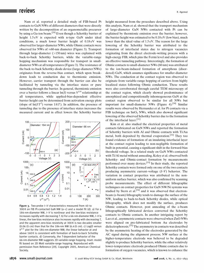
Figure 6. PL spectra of a single nanowire before (gray curve) and after
(blue curve) photoetching with defocused laser light (442 W cm�2) for
25 min in a 0.1% HF/5 g L�1 TOPO/butanol solution. For comparison,
the normalized PL spectrum of a macroscopic InP:Se crystal is plotted
(black curve). b,c) Dark-field optical and PL images of this nanowire,
respectively. Reproduced with permission from Reference [56]. Copy-
right 2005, American Chemical Society.
1878
attributed to the improvement of contacts by annealing, which
lowers the barrier heights for majority (holes) and minority
(electrons) carriers.[42] In another study of undoped Ge/Se
core/shell NWs by Xiang et al.,[43] Coulomb-blockade
behavior was observed from unannealed contacts due to the
Schottky barrier, while ballistic transport through the device
was achieved after annealing the contacts.
The ability to synthesize NWs with few defects coupled
with the formation of transparent contacts has also enabled
tunable supercurrents being observed through semiconductor
NWs.[44] Low-resistance superconducting Al electrodes on
InAs NWs were demonstrated to produce proximity-induced
supercurrents below 1K.[44] Supercurrent reversal in quantum
dots created by local gating of InAs NWs contacted by
superconducting Al electrodes was also achieved.[45] In a
recent paper, hole-carrier gas formed at the interface of a Si/
Ge core/shell NW structure was used to produce supercurrents
with Al electrodes.[46] All of these reports clearly demonstrate
the unique properties that can be achieved by using novel
nanostructures in combination with top-down fabrication
technology and open up exciting new opportunities to tune the
physical behavior of systems by chemical composition, size,
and geometry control along with controlling the contact
properties by choosing the right metal and processing
conditions.
4. NW–Dielectric Interfacial Properties
The presence of a large surface in NWs influences its
electronic and optical properties and the semiconductor–
dielectric interface becomes one of the most important
interfaces that includes interaction of the NW with air–
vacuum and all kinds of dielectrics. Therefore, the under-
www.small-journal.com � 2008 Wiley-VCH Verlag Gm
standing and control of the semiconductor–dielectric interface
becomes crucial in fabricating devices with the desired
electronic/optical response.
Photoluminescence (PL) data collected from direct-
bandgap NWs reveal a wealth of information about the
optical and electronic properties such as band-edge emission,
trap states, radiative efficiency, and carrier and photon
confinement, which are related to the surface properties. A
variety of NWs made from materials including ZnO,[47,48]
ZnS,[49] GaN,[50] CdS,[51] CdSe,[52]ZnSe,[53] InP,[54–57]
GaAs,[58] and InN[59] have been extensively studied by PL
spectroscopy. High-quality NWs typically emit brightly with a
spectral peak near the band edge. The width of the PL spectra
reveals critical information about the quality of the NWs with
narrow widths (�20–30 nm) corresponding to high optical
quality of NWs mostly due to better surface properties, and
fewer shallow impurities.
The systematic study of the influence of a NW’s surface on
its optical properties has until recently been a relatively
neglected research area.[60,61] The combination of a large
number of defect sites and high mobility of charge carriers and
surface charges[62,63] leads to the unfortunate situation that a
single surface-defect site can quench the PL of the wire over
distances in the micrometer range.[64] Efforts to (photo)-
chemically passivate the surface of NWs, analogous to
quantum-dot surface passivation,[65,66] have been mainly
focused on InP NWs. Chemisorption of oxygen on the surface
of InP NWs leads to the formation of sub-bandgap states,
creating non-radiative recombination pathways.[67] The PL
yield of InP NWs with diameters in the 50–100-nm range could
successfully be enhanced using a photochemical treatment
with HF and TOP/TOPO ligands[55,56] (Figure 6), although a
more recent study shows that this approach does not work for
InP NWs with diameters in the quantum-confinement
regime.[68] For ZnO NWs, it has been shown that addition
of a capping layer of SnO2 enhances the UV band-edge
emission.[69] Additionally, several studies have also shown the
influence of surface charges on PL peak positions.[56,63]
Whereas for light-emitting applications the influence of the
NW surface on the luminescent properties can be a
bH & Co. KGaA, Weinheim small 2008, 4, No. 11, 1872–1893

Heterointerfaces in Semiconductor Nanowires
disadvantage, it can be advantageous for utilizing NWs as
optical sensors. In a study on the effect of adsorption of gasses
on the PL of ZnSe NWs, it was found that H2 promoted the
band-edge emission whereas Ar and N2 lowered its intensity.
These changes proved reversible, leading to the proposition of
using these NWs as gas sensors.[70] Likewise, the PL fromZnO
NWs could be reversibly quenched by adsorption of NO2 on its
surface[71] and Cu2þ ions in aqueous solution proved to
specifically quench the PL from CdTe NWs.[72] While the
aforementioned optical NW sensors rely on a global intensity
effect as a detection signal, a more advanced sensing scheme
allows for spectroscopy of molecules in the vicinity of the NW
surface. When light is guided through a NW, a large fraction of
the electromagnetic field travels outside of the NW as
evanescent field. Using this evanescent field, only molecules
present in the surface-interface region are sampled, leading to
high spatial selectivity. It was shown using SnO2 NWs with
evanescent field, absorption, and surface-enhanced Raman
spectroscopy (SERS) are feasible, promising to further reduce
analyte detection limits.[73–75]
Interface states have pronounced effects on the nature and
efficacy of charge-carrier transport in FETs, an effect more
significant for nanostructures.[76] The high density of surface
states can lead to Fermi-level pinning, thereby depleting the
carriers from near the surface, an effect with profound
consequences for small-diameter NWs.[60,77] Due to the
presence of surface states and charges, the efficacy of the
gate control becomes smaller, leads to surface recombination
of carriers, and also causes hysteresis due to charge–discharge
transients from the surface states. Interface traps are produced
due to a variety of reasons including interruption of the
periodic lattice structure at the surface, broken bonds,
impurities, vacancies, and non-stoichiometric compounds,
which can trap charges. Calculations of the electronic states
of donor and acceptor impurities in semiconductor NWs
revealed that their electronic structure strongly depends on
their dielectric surrounding and on the diameter of the
wires.[78] It was predicted that the ionization energy of the
impurities in NWs is enhanced with respect to the bulk
material when the wires are embedded in a low-dielectric-
constant material, while for very small diameter NWs
(<10 nm), the ionization of impurities at 300K is reduced
and heavy doping would be necessary to obtain large
conductivity.[78] For a Si/SiO2 interface, one of the most
important interfaces for metal–oxide semiconductor field-
effect transistor (MOSFET) devices, one can distinguish
between charges located deep inside the oxide (oxide-trapped
charges and mobile ionic charges) and charges located at the
interface (fixed oxide charges and interface trap charges).[79]
The fixed oxide charges at the interface do not interact with Si
through charge transfer and therefore do not depend on the
Fermi level. On the other hand, the interface trap charges
interact with Si via charge transfer and depend on the density
of the interface states. Schmidt et al. have recently discussed
the influence of the Si/SiO2 interface on the charge-carrier
density of n-Si NWs by using simple theoretical models.[80]
Their model predicted that a NW can be fully depleted when
its radius is smaller than their calculated critical radius, which
depends on the trap-level density and doping density. For
small 2008, 4, No. 11, 1872–1893 � 2008 Wiley-VCH Verlag Gmb
example, according to their model a 50-nm Si NW is expected
to get fully depleted assuming a moderate trap density of
1011 eV�1 cm�2 if the doping is below 3� 1016 cm�3.[80]
Depletion of carriers in Si NWs would occur due to the
trapping of the free carriers at the Si/SiO2 interface and should
be avoided in order to design efficient devices. Schmidt et al.
also derived a numerical expression for the carrier density in
the presence of trap states and fixed oxide charges and their
model provides important insights regarding the effect of the
Si/SiO2 interface on transport properties of NWs, with the
most important conclusion that the carrier density in Si NWs is
in general lower than the doping concentration.[80]
Wang et al. performed a 3D quantum-transport simulation
of small (sub-10 nm) Si NWs to study the effect of Si/SiO2
interface roughness on device characteristics.[81] Their simula-
tion results predicted that the surface scattering reduces the
electron density of states in the channel, which increases the
threshold voltage. In general, the surface-roughness scattering
was found to be less detrimental in NWs that are in the
quantum-transport regime due to the availability of fewer
propagating modes in comparison to planar MOSFETs with
many occupied modes.[81] Paul et al. did a comparative study
of the impact of process variability inherent in any
semiconductor processing on the performance of NW, NT,
and MOSFET devices.[82] They observed that NTs and NWs
were least affected by almost every process and geometry-
related parameter variation such as oxide thickness and gate
width, while the MOSFET devices (45- and 32-nm technol-
ogies) were dramatically affected. They attributed the
resilience of nanostructure devices on their unique cylindrical
electrostatic geometry and novel device structures.[82]
Typically, capacitance or conductance measurements are
used to measure the interface-trap density.[79] The conduc-
tance measurements are known to provide more accurate
results while the capacitance measurements provide a rapid
estimate of the flat-band potential and the interface-trap
charge. However, the capacitance of NWs is extremely small
due to their small size, which makes capacitance–voltage
(C–V) measurements very difficult, although recent advances
in measurement technology have made such experiments
possible.[83] Dayeh et al. studied the effect of surface states on
the transport properties of InAs NW transistors with ZrO2/
Y2O3 gate dielectric by steady and time-resolved I–V
measurements.[84] InAs, as mentioned previously, forms
Ohmic contacts due to Fermi-level pinning in the conduction
band caused by donor-type surface states and surface
reconstruction, and is therefore a good system to study the
effect of surface states on transport properties. Transport
characteristics of InAs NWs were found to be heavily
dependent on the gate-voltage sweep rate, while the time-
resolved data showed surface trapping and detrapping time
scales of 45 seconds. Slower gate-voltage sweep leads to a
charge-neutral interface with reduced capacitance and higher
transconductance with small hysteresis, all of which are
desired properties. The surface trap density was estimated to
be �1012 cm�2 and the importance of passivating the surface
was clearly identified.[85] The effect of surface traps on
transport properties of ZnO NW transistors were also studied
carefully by Xiong et al. by measuring the random telegraph
H & Co. KGaA, Weinheim www.small-journal.com 1879

reviews R. Agarwal
Figure 7. a) Raw drain current random telegraph signals for a time interval of 300 s observed
in a ZnO nanowire FET at 4.2 K as a function of gate bias. The drain bias is kept constant at 2 V.
b) Histograms of the time-domain RTS data. The large and small peaks represent the empty or
filled trap states, respectively. c) Band diagram for back gate voltage at 9 V with two near
interface oxide (border) traps. Reproduced with permission from Reference [86]. Copyright
2007, American Institute of Physics.
1880
signals (RTS) for defect characterization at low temperatures
(Figure 7).[86] It is known from work done on MOSFETs that
the presence of a large number of trapping and detrapping
processes with a broad distribution of timescales produces a
1/f-type noise spectra, while in submicrometer devices the
individual traps assume importance and produce discrete
switching events and RTS.[87] For the case of n-ZnO NW
transistors assembled on a 100-nm-thick SiO2 layer with the
bottom-gate electrode, Xiong et al. observed 1/f-type noise
characteristics at room temperature while at lower tempera-
tures the noise spectra changed to Lorentzian type with
current traces displaying RTS attributed to correlated carrier
number and mobility fluctuations due to trapping and
detrapping of carriers.[86] Three-level switching events were
also observed, therefore allowing the determination of two
distinct trap states close to the Fermi level in the ZnO NW
channel. This study demonstrated the importance of quantify-
ing the noise spectra to understand the energetics and spatial
location of interface states and their effects on the transport
characteristics of NW devices, an area that still requires
detailed research.
It is expected that high-k gate dielectric materials should
increase the coupling of the gate electrode with the NW,
thereby enhancing the transistor performance. Gnani et al.
simulated the mobility and on-currents for cylindrical NWs
with SiO2 and HfO2 gate dielectrics of equal thickness and
predicted that HfO2 leads to a slight degradation of the short-
channel effect compared with the SiO2 gate but can give an
improved on-current due to lateral capacitive-coupling
effects.[88] Dai and co-workers were the first to report Ge
NW transistors with HfO2 gate dielectric deposited by atomic-
layer deposition;[89] however, the performance was degraded
in comparison to SiO2, which they attributed to interfacial
traps. Recently, the Lieber group has demonstrated superior
transistor performance by using conformal ZrO2 gate
dielectric in comparison to SiO2.[43] In addition, some
attention has been paid to other gate materials in thin films,
www.small-journal.com � 2008 Wiley-VCH Verlag GmbH & Co. KGaA, Weinhe
such as Nb2O5, Dy2O3,[90–94] although
research on the effects of these novel
dielectrics on NWs is still lacking.
The unique cylindrical geometry of
NWs can be used to create a surrounding
gate structure that can give much better
transistor properties such as improved
subthreshold behavior and higher currents
through better electrostatic gate control
through higher capacitance. It has been
experimentally demonstrated that even
conformal top gate structure can elicit
improved response fromNW transistors.[43]
Dai and co-workers have recently demon-
strated that completely surround-gated
NW transistors exhibit higher capacitance
and better electrostatic gate control than
top- and bottom-gated devices.[83] Recently
there has been interest in configuring
vertical-surround-gate NW FETs as it
allows in addition to superior electrical
properties the potential to assemble high-
density devices by utilizing the sub-lithographic dimensions of
NWs (diameters).[95–98] Even though the research in this area
is still emerging, the results are promising and will be of
continuing interest to the scientific community.
The interface between inorganic nanowires with organic or
polymeric systems is also important for fundamental under-
standing and novel applications. Combining two different
classes of material with the idea of using superior electronic
properties of inorganics with the processing versatility of
organics is exciting but needs considerable scientific attention
for developing techniques to assemble these hybrids and study
the novel interfacial properties. For example, single ZnONW-
FETs fabricated using self-assembled organic gate dielectric
displayed outstanding device-performance metrics demon-
strating enhancement-mode ZnO NW-FETs operating at sub-
1V with exceptionally high on/off current ratios.[99] It was
observed that ozone-treated ZnO NW-FETs consistently
retained the enhanced device-performance metrics after SiO2
passivation. Two interesting polymer/nanowire systems cur-
rently under investigation for photovoltaic applications are
ZnO/P3HT/PCBM[100–105] and CdS(CdSe)/P3HT[106–113] with
a staggered band alignment. In ZnO systems[102,103] the proper
blending of P3HT and PCBM was speculated to decrease the
path that excitons travel before being split, thereby decreasing
their chance of recombination and improving the performance
of the device. Developments in CdS and CdSe/polymer
nanocomposites have centered around the role of ligands on
the semiconductor wire in the development of photovoltaic
devices. Specifically, the predominant message in the current
literature indicates that polymer/nanowire composites that
include pyridine in the solution processing will create devices
with improved fill factor and conversion efficiency.[106–112]
Wang et al.[106] studied MEH-PPV/CdS nanowire systems and
found that adding pyridine to their chlorobenzene solutions
increased short-circuit current in the resulting devices by a
factor of 6 over systems without pyridine. They speculate that
pyridine improves the dispersion of CdS in solution and thus
im small 2008, 4, No. 11, 1872–1893

Heterointerfaces in Semiconductor Nanowires
increases charge transfer and exciton dissociation, as seen by
improved PL quenching over devices prepared without
pyridine. Complimentary research done by Huynh and co-
workers[107] suggests thermal treatment may drive off pyridine
adsorbed on the surface of the nanowire, thus creating a more
efficient path for exciton splitting. The nature of the
conduction mechanism at the interface and in the nanocom-
posite in general has been investigated by several groups. Xi
et al.[109] grew CdS nanowires within PANI sheaths by
electrodeposition in order to study the charge-transfer
mechanism between polymer and CdS. Intensity of the PL
of the core/shell composite was seen to increase by 4.5 times.
They concluded that the increase in PL could not be explained
by the Forster or Dexter transfer mechanisms and that the
actual mechanism of PL enhancement is the proper alignment
of band edges in PANI and CdS, allowing for efficient
transport of photogenerated electrons to the CdS core and
thereby increasing its PL. Yu et al.[112] and Lai et al.[113] have
shown tunable light-emitting diode (LED) and FET nanowire/
polymer systems. Overall, research in nanowire/polymer
composites has shown promise in creating viable LED and
photovoltaic (PV) devices. However, the current research
underscores the importance of blend homogeneity and
processing conditions on the interface in these devices in
order to eliminate potential sites for undesirable recombina-
tion.
Control of NW surface properties is therefore extremely
important for all kinds of devices. For example, for NW
chemical/biological sensors based on FETs the surface has to
be appropriately functionalized with chemical or biological
receptors to achieve high selectivity and sensitivity for analyte
detection, which in turn requires knowledge about the surface
properties.[114,115] The polar surfaces of ZnO NWs are critical
for the generation of piezoelectric effects, which are getting
attention currently.[116,117] In a recently reported electric-field-
induced reversible crystalline-to-amorphous phase change in
chalcogenide NWs[118–120] the interaction of the NW with its
surroundings determines the efficiency of the phase transition.
The surrounding material has to have large heat capacity and
thermal conductivity in order to rapidly cool the NW
undergoing the phase change. As of now no detailed attention
has been devoted to the effect of NW surface and encapsula-
tion on the nature and efficiency of phase transition, an
important consideration for fundamental studies of nanoscale
heat generation and propagation and also for fabrication of
next-generation phase-change memory devices.
5. Crossed-NW Devices
Cross-bar technology from top-town lithographically
defined structures has been utilized for memory switches in
conventional electronics. A similar concept can also be
applied by creating architectures of crossed NWs, resulting
in truly nanoscale junctions at each crossing, which can
have unique encoded functionalities including transistors,
diodes, memory, address decoder, or tunneling junctions. The
device functionality, which originates from lithography-free
nanoscale junctions, can be as small as a few hundred atoms
small 2008, 4, No. 11, 1872–1893 � 2008 Wiley-VCH Verlag Gmb
and can be further enhanced by combining NWs of different
compositions and doping profiles. One of the first demonstra-
tions of crossed NW structure was reported by Heath and co-
workers,[121] where they assembled two Si NWs to fabricate a
four-terminal device. The resistivity through the crossed-wire
junction was measured to be similar to the resistivity of
individual wires forming the crossed device, indicating little or
no tunneling barrier at the junction of the two wires,
suggesting the absence of SiO2 at the junction. Thus, these
two crossed wires functioned as a single conducting unit.
The Lieber group has developed an impressive set of tools
to reliably manipulate NWs to assemble them into crossed
architectures[25,26] and has also demonstrated unique device
functionalities originating from combining NWs from a variety
of materials. One of the first devices reported by the Lieber
group was a p–n-junction diode from Si NWs, with controlled
dopant concentrations.[122,123] Subsequently, LEDs from p-
and n-doped crossed InP NWs (Figure 8) were reported[26]
and, more recently, from n-GaN/p-GaN,[125] which demon-
strated that it is possible to produce light from such nanoscale
junctions. Electrical measurements from the nanoscale diodes
showed clear rectification behavior, and electroluminescence
(EL) spectra showed emission from the band edge. In
addition, the demonstration of band-edge emission from cross
junction formed between a direct-bandgap NW with a Si NW
clearly demonstrated the versatility of this approach in
combining different materials to assemble functional archi-
tectures. For example, nanoscale LEDs assembled from n-
CdS, n-GaN, and n-CdSe NWs with p-Si NWs have been
successfully demonstrated.[124] In addition, integration of
nanoscale LEDs from these NWmaterials with a common p-Si
NW was also configured, which showed the potential of
assembling multicolor LEDs on a common platform
(Figure 8), a task which is otherwise difficult for top-down
fabricated devices.[124] Recently, Hayden et al. have also
demonstrated the use of localized light emission from crossed
NW LEDs from p-Si/n-CdS for fluorescence spectroscopy and
cellular imaging.[126] The extremely localized excitation source
can in principle excite femtoliter quantities of fluids, thereby
opening up possibilities for highly sensitive imaging and
spectroscopy using NW devices.
Crossed NW diodes can also be used as photodetectors
under reverse bias. In a recent demonstration, crossed p-Si/n-
CdS NW diodes were assembled with the dopant concentra-
tion in a p-Si NWkept very low to increase the depletion width
at the junction to engineer avalanche multiplication and
breakdown under reverse bias (Figure 9).[127] The device
under reverse bias showed exceptionally low dark currents
(<100 pA) with a sharp breakdown occurring at ��9.0V
(Figure 9a). Upon illuminating the device with light, a large
reverse-bias-dependent photocurrent was observed, which is
indicative of avalanche breakdown phenomenon with a
multiplication factor estimated to be �5� 104. Spatially
resolved photocurrent measurements (Figure 9b) performed
on the devices revealed a single, highly localized photocurrent
peak located at the position of the crossed NW p–n junction
with a spatial resolution of �250 nm, thereby demonstrating
that the detector has subwavelength spatial-resolution cap-
abilities with an estimated sensitivity of �75 photons. This
H & Co. KGaA, Weinheim www.small-journal.com 1881

reviews R. Agarwal
Figure 8. a) I–V behavior of n–n, p–p, and p–n junctions of crossed n- and p-InP nanowires.
The green and blue curves correspond to the I–V behavior of individual n- and p-type
nanowires in the junction, respectively. The red curves represent the I–V behavior across the
junctions. Reproduced with permission from Reference [26]. Copyright 2001, Nature Pub-
lishing Group. b) EL spectra from crossed p–n diodes of p-Si and n-CdS, CdSSe, CdSe, and InP
(top to bottom, respectively). Insets to the left are the corresponding EL images for CdS,
CdSSe, CdSe, and InP nanowire LEDs. The top-right inset shows representative I–V and SEM
data recorded for a p-Si/n-CdS crossed NW junction (scale bar 1mm). c) Schematic and
corresponding SEM image of a tricolor nano-LED array. d) Normalized EL spectra and color
images from the three elements. Reproduced with permission from Reference [124].
1882
very high sensitivity is due to the large avalanche multi-
plication effect, which compensates for the low photon-
absorption cross section of nanoscale detectors. Larger arrays
with independently addressable avalanche photodiodes
(APDs) (Figure 9c) were also demonstrated, an essential
feature to enable future-generation integrated photonics.[127]
Crossed-NW architecture has also been utilized by Huang
et al. to assemble FETs, with one NW configured as the active
channel with a dielectric gate-oxide shell and the other NWs
functioning as local gate electrodes.[128] For example,
transistor-like properties were obtained from a Si NW
functioning as the p-channel with a SiO2 shell crossed with
a GaN NW acting as the gate electrode. Extending this
approach, threeGaNNWswere subsequently crossed with a Si
NW to assemble logic gates such as a two-input and two-output
AND and NOR logic gates and other basic computation was
demonstrated with signal gain (Figure 10a).[128] This experi-
Figure 9. a) Characterization of nanowire APDs. a) I–V characteristic of the APD in dark (black li
inset shows an SEM image of the crossed n-CdS/p-Si device (scale bar 4mm). b) Plot of the spa
measured in proportional mode using a diffraction-limited laser; the bias voltage, laser power, and
(in x and y), respectively. The nanowire positions are indicated on the plot by solid lines. c) Spatiall
(a). Both devices were biased at�10 V and excited at 488 nm (200 nW, Arþ ion laser) with a scannin
device consisting of an n-CdS nanowire (horizontal) crossing two p-Si nanowires (vertical); the la
contacts (scale bar 10mm). Reproduced with permission from Reference [127]. Copyright 2006,
www.small-journal.com � 2008 Wiley-VCH Verlag GmbH & Co. KGaA, Weinhe
ment demonstrated the feasibility of using
crossed semiconductor NW architectures in
assembling functional nanoelectronic cir-
cuits.
Even though the device functionality
originating from crossed NW architectures
is extremely small in length scale, the
assembly of integrated architectures for
nanoelectronics and photonics will require
schemes for addressing individual elements
within the nanoscale arrays. Zhong
et al.[129] have reported an approach to
circumvent this problem based upon a
scalable crossed-NW FET architecture, in
which chemical modification of specific
cross points within the array was used to
define address codes that enables NW input
lines to turn on/off specific output lines
(Figure 10d).[129] This basic array structure
thus functions as an address decoder, with
electronic gain originating from the crossed
NWFETs that can restore the electrical signal. Beckman et al.
demonstrated an innovative demultiplexer architecture for
bridging from submicrometer to nanometer-scale dimensions
for the selective addressing of ultrahigh-density NW circuits
on an array of 150 Si NWs patterned at widths of 13 nm and a
pitch of 34 nm crossed with metal NWs.[130]
Although important demonstrations have been made
utilizing the crossed-NW architecture, there is not much
information about the nature of carrier transport across the
crossed junction. In order to quantitatively model the junction
behavior, information regarding the geometry, oxide thick-
ness, defects, and impurities present at the junction need to be
determined, which is experimentally challenging. Lack of such
detailed information has impeded efforts on the theoretical
front to understand the nature of charge transport at the
crossed junction.Wei et al.[131] have attempted to qualitatively
model the junction behavior by using a tight-binding model
ne) and illuminated (red line) conditions. The
tially resolved photocurrent from the nano-APD
scanning step size were�7 V, 200 nW, and 250 nm
y resolved photocurrent measured from the array in
g step size of 1mm. Inset: Optical micrograph of the
rger rectangular features correspond to metal
Nature Publishing Group.
im small 2008, 4, No. 11, 1872–1893
Heterointerfaces in Semiconductor Nanowires
Figure 10. a) Schematic image of logic AND gate assembled from a
1� 3 crossed NW junction array. Inset: A typical SEM (scale bar 1mm) of
the assembled AND gate and symbolic electronic circuit. b) The output
voltage versus the four possible logic address level inputs. Inset: The
V0–Vi, where the solid and dashed red (blue) lines correspond to V0–Vi1and V0–Vi2 when the other input is 0 (1). c) The experimental truth table
for the AND gate. d) SEM image of a 4� 4 crossed Si NW array address
decoder, with four horizontal NWs (I1 to I4) as inputs and four vertical
NWs (O1 to O4) as signal outputs. The four diagonal cross points in the
array were chemically modified to differentiate their responses from the
input gate lines (scale bar 1mm). e) Real-time monitoring of the Vg
inputs (blue) and signal outputs (red) for the four-by-four decoder.
Reproduced with permission from References [128, 129]. Copyright
2001 and 2003, respectively, American Association for the Advance-
ment of Science.
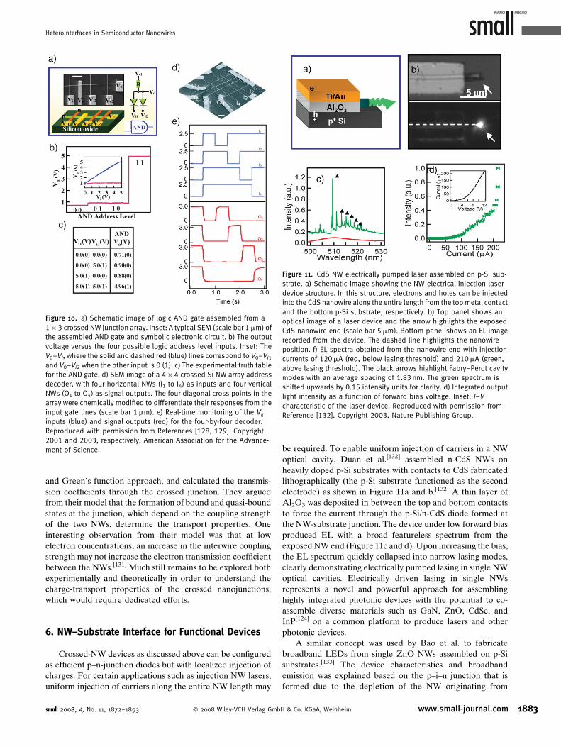
Figure 11. CdS NW electrically pumped laser assembled on p-Si sub-
strate. a) Schematic image showing the NW electrical-injection laser
device structure. In this structure, electrons and holes can be injected
into the CdS nanowire along the entire length from the top metal contact
and the bottom p-Si substrate, respectively. b) Top panel shows an
optical image of a laser device and the arrow highlights the exposed
CdS nanowire end (scale bar 5mm). Bottom panel shows an EL image
recorded from the device. The dashed line highlights the nanowire
position. f) EL spectra obtained from the nanowire end with injection
currents of 120mA (red, below lasing threshold) and 210mA (green,
above lasing threshold). The black arrows highlight Fabry–Perot cavity
modes with an average spacing of 1.83 nm. The green spectrum is
shifted upwards by 0.15 intensity units for clarity. d) Integrated output
light intensity as a function of forward bias voltage. Inset: I–V
characteristic of the laser device. Reproduced with permission from
Reference [132]. Copyright 2003, Nature Publishing Group.
and Green’s function approach, and calculated the transmis-
sion coefficients through the crossed junction. They argued
from their model that the formation of bound and quasi-bound
states at the junction, which depend on the coupling strength
of the two NWs, determine the transport properties. One
interesting observation from their model was that at low
electron concentrations, an increase in the interwire coupling
strength may not increase the electron transmission coefficient
between the NWs.[131] Much still remains to be explored both
experimentally and theoretically in order to understand the
charge-transport properties of the crossed nanojunctions,
which would require dedicated efforts.
6. NW–Substrate Interface for Functional Devices
Crossed-NW devices as discussed above can be configured
as efficient p–n-junction diodes but with localized injection of
charges. For certain applications such as injection NW lasers,
uniform injection of carriers along the entire NW length may
small 2008, 4, No. 11, 1872–1893 � 2008 Wiley-VCH Verlag Gmb
be required. To enable uniform injection of carriers in a NW
optical cavity, Duan et al.[132] assembled n-CdS NWs on
heavily doped p-Si substrates with contacts to CdS fabricated
lithographically (the p-Si substrate functioned as the second
electrode) as shown in Figure 11a and b.[132] A thin layer of
Al2O3 was deposited in between the top and bottom contacts
to force the current through the p-Si/n-CdS diode formed at
the NW-substrate junction. The device under low forward bias
produced EL with a broad featureless spectrum from the
exposed NW end (Figure 11c and d). Upon increasing the bias,
the EL spectrum quickly collapsed into narrow lasing modes,
clearly demonstrating electrically pumped lasing in single NW
optical cavities. Electrically driven lasing in single NWs
represents a novel and powerful approach for assembling
highly integrated photonic devices with the potential to co-
assemble diverse materials such as GaN, ZnO, CdSe, and
InP[124] on a common platform to produce lasers and other
photonic devices.
A similar concept was used by Bao et al. to fabricate
broadband LEDs from single ZnO NWs assembled on p-Si
substrates.[133] The device characteristics and broadband
emission was explained based on the p–i–n junction that is
formed due to the depletion of the NW originating from
H & Co. KGaA, Weinheim www.small-journal.com 1883

reviews R. Agarwal
Figure 12. SEM image of a) n-GaN nanowire/p-Si light-emitting diode.
Inset: zoomed-in image of the nanowire end. b) Forward-bias EL spectra
of the device at 77 K (black) and at 295 K (gray). Both traces were
obtained with the same applied bias of þ5.4 V and currents of 150mA at
77 K and 165mA at room temperature. Inset: plot of integrated intensity
versus current at 77 K (black) and 295 K (gray). c) Reverse-bias EL
spectrum for n-GaN nanowire/p-Si device. Reproduced with permission
from Reference [134]. Copyright 2007, Institute of Physics and IOP
Publishing Limited.
1884
oxygen adsorption on the NW surface. The broadband
emission was attributed to defects and surface states although
some emission from exciton recombination was also observed.
Zimmler et al.[134] recently performed a systematic electrical
study of n-GaNNWassembled on an n-Si substrate where they
observed that by reversing the polarity of the applied voltage
the EL can be selectively obtained from either the NW or the
substrate (Figure 12). For one polarity of the applied voltage,
UV and visible light were generated in the GaNNW, while for
the opposite polarity infrared light was emitted from the Si
substrate. A model, which took into account the oxidation of
GaN NW surface and Si substrate and was able to explain the
key features of the data based on electron tunneling from the
valence band of one semiconductor into the conduction band
of the other semiconductor. For example, for one polarity of
the applied voltage, given a sufficient potential-energy
difference between the two semiconductors, electrons can
tunnel from the valence band of GaN into the Si conduction
band, resulting in the creation of holes in GaN, which can
recombine with conduction-band electrons generating GaN
band-to-band luminescence.[134] This device structure affords
an additional experimental handle to the study of EL in single
NWs and, furthermore, could be used as a novel approach to
two-color light-emitting devices.
7. Axial Heterostructures
One of the first demonstrations of modulation of dopant
concentrations along a NW was reported by Wagner et al. in
1970s.[135] In 1992 Haraguchi et al.[136] reported assembly of p–
n junctions in GaAs NWs of �100-nm diameter using gold
particles as a catalyst, which showed rectification and EL that
was polarized along the NW long axis. C–V measurements
were also performed, which indicated formation of abrupt
junctions, while analysis of I–V behavior suggested formation
of junctions with 60-nm diameter due the formation of a
surface-depletion layer. However, the measurements were not
performed on individual NWs but on large arrays, which
limited the detailed understanding of the behavior of
nanoscale p–n junctions in axial geometry.
There was renewed interest in NW axial heterostructures
when their controlled synthesis was reported in 2002
by the Lieber,[137] Yang,[138] and Samuelson groups.[23]
The Samuelson group reported axial heterostructures with
atomically sharp interfaces, using chemical beam epitaxy
(CBE). The laser ablation and chemical vapor deposition
(CVD) techniques used by the Lieber[137] andYang groups[138]
produced compositionally graded interfaces. The main reason
for compositionally broadened interfaces is the retention of
the first constituent in the catalyst causing mixing of the two
components.
The nature of the heterointerface determines the proper-
ties of the NW heterostructure device. The Si-SiGe super-
lattice structures reported by Yang and co-workers did not
have abrupt interfaces but a broad alloyed region, which
was determined to be responsible for phonon scattering
instead of the desirable scattering from the heterointerfaces
for thermoelectric applications.[139] The axial heterostructures
www.small-journal.com � 2008 Wiley-VCH Verlag GmbH & Co. KGaA, Weinheim small 2008, 4, No. 11, 1872–1893

Heterointerfaces in Semiconductor Nanowires
synthesized by Lieber and co-workers (GaP-GaAs)[137] were
also not abrupt with the alloying region directly proportional
to the diameter of the nanocatalyst used for the NW growth.
PL spectra from the multisegmented GaP-GaAs NW showed
emission from GaAs components only with no emission
observed from the indirect bandgap of GaP segments.
The Lieber group also fabricated axial p–n junctions in Si
NWs and measured the electrical properties of single NW
devices.[137] The I–V curve displayed rectification (Figure 13a),
the spatial origin of which was characterized by scanning
probe measurements indicating abrupt transition (instrument-
resolution limited) in carrier type and the accompanying
built-in potential at the physical p–n junction in the NW.
Moreover, intra-NW p-n junction in single InP NW devices
also showed EL under forward bias from the junction region.
Cheng et al.[141] also demonstrated the formation of axial p–n
junctions in single GaN NW devices, with temperature-
dependent measurements of I–V characteristics being con-
igure 13. Axial modulation-doped Si nanowires. a) Rectification behavior observed for
n axial p–n Si nanowire junction. Inset: electrical characterization by scanning probe
icroscopy and a scanning electron micrograph of the silicon nanowire device with source (S)
nd drain (D) electrodes. b) Scanning gate microscopy images of nþ-(n-nþ)N nanowires where
) N¼ 3, (B) N¼6, and (C) N¼ 8 are the periods. c) SEM image of a 2�2 decoder configured
sing two modulation-doped silicon nanowires as outputs (Out1 and Out2) and two Au metal
ates, which were deposited using e-beam lithography functioning as inputs (In1 and In2;
cale bar 1mm). Plots of input (blue) and output (red) voltages for the 2�2 decoder,
emonstrating selective addressing by Inputs 1 and 2. d) Coupled quantum-dot structures
ith a variable width barrier defined by synthesis; top) the device with the largest barrier
xhibits a single Coulomb oscillation period showing that the two quantum dots are weakly
oupled; middle) the intermediate-width barrier exhibits a splitting of each of the Coulomb
scillation peaks into doublets, which is the signature of enhanced tunneling conductance
etween the quantum dots; bottom) further reduction of the barrier width again produces
ingle Coulomb oscillation period with the effective quantum-dot size twice that of the
dividual quantum-dot regions, implying that the structures are fully delocalized.
eproduced with permission from Reference [140]. Copyright 2005, American Association
r the Advancement of Science.
F
a
m
a
(A
u
g
s
d
w
e
c
o
b
s
in
R
fo
small 2008, 4, No. 11, 1872–1893 � 2008 Wiley-VCH Verlag Gmb
sistent with electron tunneling through a voltage-dependent
barrier; however, the EL was not reported.
There have been multiple reports of formation of single-
crystalline axial heterojunctions between Si NW and NiSi by
solid-state transformation reactions (discussed in Section 3),
where the nature of nanoscale junctions has been shown to
produce superior device characteristics.[39,40] The concept of
modulation doping of Si NWs along their lengths with
different dopant types and concentrations was utilized by
Yang et al.[140] to assemble address decoders to bridge the
macro- to nanoscale size scale. Growth of nþ–n–nþ repeat
structures axially along Si NW length with control over size
and periodicity was achieved and studied by scanning gate
microscopy, which demonstrated well-defined dopant regions
of varying concentration (Figure 13b). A prototype address
decoder device was demonstrated with two Si-modulation-
doped NWs and microscale address wires (lithographically
defined) functioning as inputs and outputs, respectively
H & Co. KGaA, Weinheim
(Figure 13c). In the same publication, Yang
et al. also demonstrated control over the
size and separation of doped regions to
confine single and multiple quantum dots
by exploiting the different band offsets
formed by dopant variations.[140] By vary-
ing the separation between the confined
dots and the barrier heights, different
intradot coupling strengths were clearly
observed (Figure 13d), which demonstrated
the advantage of chemical synthesis over
lithography to control and encode different
device functionalities. In another report,
Yang et al.[142] also demonstrated the
formation of controlled axial p–i–n junc-
tions in Si NWs. Temperature-dependent
I–Vmeasurements recorded from individual
p–i–n devices showed an increase in the
breakdown voltage with temperature, char-
acteristic of avalanche breakdown. Spa-
tially resolved photocurrent measurements
showed that the largest photocurrent is
generated at the intrinsic region located
between the electrode contacts, with multi-
plication factors of 30.[142] Electron- and
hole-initiated avalanche gain measure-
ments performed by localized photoexcita-
tion of the p-type and n-type regions
yielded multiplication factors of 100 and
20, respectively, implying that the ioniza-
tion rate for electrons is significantly higher
than that for holes, in agreement with
conventional planar silicon APDs. One can
envision changing the dopant concentration
and length of different segments to pre-
cisely engineer the electric-field profiles in
these 1D NWs to produce the desired
electronic/optoelectronic response.
One of the first demonstrations of axial
NW heterostructures with near atomically
abrupt interfaceswas reportedbySamuelson
www.small-journal.com 1885

reviews R. Agarwal
1886
and co-workers in 2002 and in their subsequent publica-
tions.[23,97,143,144] Bjork et al. were able to produce InP–InAs
superlattice structures with abrupt interfaces using ultrahigh
vacuum CBE with NW growth catalyzed by Au particles
(Figure 14).[23] The reason for abrupt interfaces was attributed
to the high vapor pressures of the group-V precursors in
combination with the low growth rate (�1 monolayer s�1). In
later papers, detailed analysis was performed in which it was
found that the gold catalyst remains solid during the entire
growth process, leading to slow growth rates and hence
excellent control over heterointerfaces with no obvious
structural defects.[145] Utilizing this level of control over the
axial heterointerfaces, InP barrier segments of varying
lengths were embedded in 40-nm-diameter InAs NWs.[143]
Temperature-dependent electrical data from these hetero-
structured NWs were modeled by assuming thermionic
Figure 14. a) HRTEM image of an InAs NW with two InP barriers. Double-
barrier resonant tunneling data for devices fabricated inside a nano-
wire. b) TEM image of the top end of a NW with the double barrier clearly
visible with a barrier thickness of �5 nm (scale bar 30 nm). c) Energy-
band diagram for the device with the electronic states in the emitter
region indicated (left). In between the two InP barriers the fully
quantized levels of the central quantum dot are indicated. d) I–V data
for the same device as shown in (b) and (c) recorded at 4.2 K, revealing a
sharp peak in the characteristics, reflecting resonant tunneling into the
ground state with a voltage width of �5 mV. This width can be
translated into an energy width of the transition of �2 meV, corre-
sponding to the width of the shaded energy band in the emitter from
which electrons tunnel. The inset provides a magnified view of the
resonance peak for increasing voltage (gray) and for decreasing voltage
(black), hence, confirming negligible hysteresis effects. Reproduced
with permission from Reference [143]. Copyright 2002, American
Institute of Physics.
www.small-journal.com � 2008 Wiley-VCH Verlag Gm
emission over the InP barrier from which a barrier height
of �0.6 eV was determined, in close agreement with the
estimated barrier height of bulk systems.[143] By changing the
barrier thickness, the tunnel resistance was shown to vary over
a very large range. The Samuelson group also synthesized a
resonant tunnel diode (RTD) embedded in an InAs NW with
an InAs quantum dot sandwiched between two InP barriers in
axial geometry (Figure 14).[143] The observation of sharp
features in the tunneling spectra, corresponding to well-
defined quantum states of the InAs dot, was enabled only due
to the abrupt interfaces between InAs and InP segments.
Thelander et al.[144,146] then assembled single electron
transistors (SETs) by changing the RTD device by increasing
the InAs dot dimensions and fabricating a gate electrode
coupled to the InAs dot. By changing the InAs dot size it was
shown by Bjork et al. that it is possible to tune the device
performance from SET to a few electron quantum dots
(Figure 15), with the tunneling spectra obtained from
transport measurements displaying unique shell structure
owing to spin and orbital degeneracy.[144] Bjork et al. reported
tunneling spectroscopy measurements of the Zeeman spin
splitting in InAs; few electron quantum dots formed between
two InP barriers.[147] They observed that the values of the
electron g factors of the first few electrons entering the dot
strongly depend on the dot size ranging from the bulk value of
InAs in large dots (jg�j¼13) down to jg�j¼2.3 for the smallest
dots.[147] Fabrication of intra-NW SETs allows continuous
tunability of device characteristics, which is otherwise not
possible with SET behavior observed in homogeneous
NWs.[148] Fabrication of RTDs and SETs with the desired
device characteristics provides an impressive demonstration
that it is possible to form novel confinement potentials using
axial interfaces within NWs.
By extending the concept of growing InAs dots between
InP barriers, Samuelson and co-workers demonstrated storage
of single and few electrons in multiple tunnel junctions
incorporated at the end of InAs wires, where the Au seed
particle functioned as the storage mode.[149] By placing
another NW in close proximity, the mechanism of charge
transfer in the NW was studied and trapping of electrons was
confirmed. In another demonstration of NWmemory based on
stacks of axial quantum dots, Nilsson et al.[150] showed
memory operation by tunneling of electrons through multiple
dots separated by barriers. The transport through the
heterostructured device was shown to be tunable by applied
bias due to misalignment of the energy levels leading to
hysteresis of charging/discharging of the storage island.[150]
One of the challenges in developing devices based on quantum
states in NWs for quantum-information applications is the
ability to detect and measure the charge states on the quantum
dots. Wallin et al.[151] demonstrated the operation of a charge-
readout scheme for InAs dots defined between InP barriers in
InAs NW using a quantum-point contact defined in a GaAs/
AlGaAs 2D electron gas (2DEG) beneath the NW. Applying
negative voltages to two split-gate electrodes aligned to the
NW was shown to induce a quantum point contact in the
2DEG such that charging of quantum dots in the NW
modulated the quantum point contact transmission, resulting
in the desired detector response.[151]
bH & Co. KGaA, Weinheim small 2008, 4, No. 11, 1872–1893

Heterointerfaces in Semiconductor Nanowires
Figure 15. a) left: Dark-field scanning TEM image of a nanowire with a 100-nm-long InAs
quantum dot between two very thin InP barriers (scale bar 20 nm). Right: corresponding
image of a 10-nm-long InAs dot. The InP barrier thickness is 3 and 3.7 nm, respectively. Effect
of reduced quantum-dot length on transport properties; b) gate characteristics of a
single-electron transistor (SET) with a 100-nm-long dot. The oscillations are periodic. c) When
the dot length is 30 nm, the level spacing at the Fermi energy is comparable to the charging
energy and the Coulomb oscillations are no longer completely periodic. d) A 10-nm dot results
in a device depleted of electrons at zero gate voltage. By increasing the electrostatic potential
electrons are added one by one. For some electron configurations the addition energy is
larger, corresponding to filled electron shells. All data were recorded at 4.2 K. Reproduced
with permission from Reference [144]. Copyright 2004, American Chemical Society.
Optical spectroscopy has also been utilized to study the
effect of quantum confinement of charge carriers in axial NW
heterostructures. PL spectra have been studied in direct-gap
systems, including ZnSe–CdSe,[152] InAs–GaAs,[153] InAs–
InP,[154] and ZnO–ZnMgO.[155] Poole et al. reported
InP–InAs–InP NW heterostructures on InP substrates without
the use of a catalyst with growth based on the preferential
diffusion of In along facets.[154] The InAs quantum-well
thickness was estimated to be 0.6 nm while quantitative
estimates of interface quality was not reported. At low
optical power, a single well-defined peak was observed at
921meV in PL spectrum. At higher powers, excited-state
peaks were observed at energy spacings consistent with the
quantum confinement of excitons corresponding to the
estimated well widths.[154] Park et al.[155] demonstrated
excellent control over the axial heterointerface between
repeated segments of ZnO–ZnMgO nanorods grown using
catalyst-free metal–organic vapor-phase epitaxy (Figure 16).
ZnO–ZnMgO interface widths of �1 nm were measured
using high-resolution transmission electron microscopy
(HRTEM) and no significant Mg diffusion. They observed a
systematic blueshift of emission with decreasing quantum-well
width in ZnO–ZnMgO multiple quantum-well heterostruc-
tures (ensemble measurement), which was modeled assuming
periodic square-well potentials for 10 period structures
(Figure 16c and d).[155] Radial confinement was not observed
as the wire diameters averaged �40 nm, which is much
small 2008, 4, No. 11, 1872–1893 � 2008 Wiley-VCH Verlag GmbH & Co. KGaA, Weinheim
greater than the exciton Bohr radius of
ZnO. In a later publication, Park et al.[156]
also measured time-resolved excited-state
decay characteristics from ZnO–ZnMgO
NW single-quantum-well samples and
observed slower decay with two time
constants (170 ps and 580 ps) from the
quantum-well emission peaks in compar-
ison to the remaining wire (56 ps and
330 ps). They attributed slower decay from
the quantum-well to size-dependent light–
matter interaction in low-dimensional sys-
tems, leading to formation of exciton–
polaritons with longer recombination life-
time than in bulk systems.[156] Even though
it is an interesting observation, more
detailed experiments and theoretical mod-
eling are required to make such claims in
complex heterostructured systems at length
scales that are smaller than the exciton
Bohr radius. Yatsui et al.[157] reported low-
temperature near-field spectroscopy of
isolated ZnO–ZnMgO single-quantum-
well structures grown on the end of ZnO
nanorods. The absorption spectra of iso-
lated quantum-well structures displayed a
small Stokes shift of 3 meV and sharp PL
peaks. Furthermore, polarization spectro-
scopy of isolated nanorod quantum wells
revealed valence-band anisotropy in PL
spectra.[157] Since the exciton in a quantum
structure is an ideal two-level system with
long coherence times, their results provided criteria for
designing nanophotonic switches, which was indeed reported
in a more recent publication.[158] By using time-resolved near-
field spectroscopy of ZnO–ZnMgO nanorod double-quantum-
well structures, they observed nutation of the population
between the resonantly coupled exciton states of the coupled
quantum dots. Optical switching dynamics were also demon-
strated by controlling the exciton excitation in the dipole-
inactive state via an optical near field.[158] Their results are a
promising step toward designing a nanometer-scale photonic
switch and related devices that utilize the quantum confine-
ment in stand-alone nanorod structures.
Kim et al.[159] have reported high-efficiency LEDs using
dislocation-free InGaN–GaN multiquantum-well NW arrays
grown on sapphire substrate. The NWs were tapered with a
diameter in the center of �70 nm and a length of �1mm and
with typical quantum-well widths of �4.8 nm with near
atomically abrupt interfaces. Due to the lack of dislocations
and the large surface areas provided by the sidewalls of NWs,
both internal and extraction efficiencies were significantly
enhanced with about 4.3 times more light than the conven-
tional broad-area LEDs. The present method of utilizing
dislocation-free NW LEDs is promising for the fabrication of
superbright-white LEDs and for improving their total external
efficiency.[159]
Panev et al.[153] observed sharp exciton-like emission from
InAs quantum dots embedded inside GaAs NW hosts grown
www.small-journal.com 1887

reviews R. Agarwal
Figure 16. a) Schematic of axial multiple quantum-well NWs consisting of 10 periods of
Zn0.8Mg0.2O/ZnO. Inset: corresponding electronic-band diagram. b) Z-contrast TEM image of a
2.5-nm-width sample clearly showing the composition variation (bright layers are ZnO wells).
c) Pl spectra at 10 K for a single-period heterostructure (top) and 10-period multiple quantum
well with varying well widths. The corresponding band diagrams are given. d) Quantum-well-
dependent peak positions (squares) along with theoretical prediction. Reproduced with
permission from Reference [155].
1888
using CBE. The authors observed growth in both axial and
radial directions, thereby producing tapered NWs that
effectively encapsulated the InAs dot within a GaAs shell,
leading to effective surface passivation resulting in increased
radiative quantum yield. The emission from the InAs dots was
significantly blueshifted from the bulk InAs, indicating that
substantial alloying with the GaAs wire had occurred in
addition to any quantum-confinement effects, which made
estimation of confinement effects rather difficult.[153] In
another interesting study, Kim et al.[160] observed formation
of embedded quantum dots in ZnO–ZnMgO multiple
quantum-well samples due to partial strain relaxation if the
number of periods exceeded a certain number (four) or the
quantum-well width exceeded 2.5 nm in thickness. Emission
from embedded quantum dots was clearly observed and their
experiments[160] showed that efficient strain relaxation in
nanoscale heterostructures is not a universal feature, as
previously believed. Borgstrom et al.[161] reported assembly of
As-rich quantum dots of �15-nm length embedded in a P-rich
GaAs/GaP NW system. Significantly, photon antibunching
was observed from quantum-dot emission proving the zero-
dimensional nature of these heterostructures, which also
opens up interesting possibilities of fabricating electrically
driven single photon sources based on the bottom-up
www.small-journal.com � 2008 Wiley-VCH Verlag GmbH & Co. KGaA, Weinhe
approach.[161] An important breakthrough
towards realizing this goal has been
reported by Minot et al.[162] where they
have been able to achieve reproducible
fabrication of InP–InAsP LEDs in which
electron–hole recombination is restricted
to a quantum-dot InAsP section confined
between n- and p-doped InP segments
(Figure 17). Rectification was observed in
I–V measurements and EL corresponding
to InAsP quantum dots was also
observed.[162] Even though several other
challenges such as emission from n- and p-
doped InP, low quantum of emission, and
better device structure need to be over-
come to assemble an electrically driven
single photon source fom NWs, this
experiment is a very critical advance
towards the final goal.
8. Radial Heterostructures
The ability to create new systems by
manipulating the growth procedures can be
extended to create NW radial heterostruc-
tures with compositional modulation in the
radial direction. To grow radial hetero-
structures, the VLS growth is minimized
and the second component grows epitaxi-
ally on the NW core. Analogous to
colloidal core/shell quantum dots,[163]
NW radial heterostructures can passivate
the surface to remove the deleterious
effects of surface states, enabling enhanced
performance of devices. For example, a shell of high-k
dielectric can enhance the performance of FETs, a ferro-
electric oxide shell can be used to fabricate non-volatile
memory, and materials with different band offsets can be
combined to create a high-mobility carrier gas, or confine
excitons in the radial direction. Core/shell structures have also
been utilized to dope the NW core via deposition of a heavily
doped shell,[164] formation of axial p–n junctions,[165] and for
the synthesis of novel nanotubes.[166,167]
The first synthesis of core/shell NW heterostructures was
reported by Lauhon et al.[24] in 2003 by using a CVD approach
to grow homo- and heterostructures from Si and Ge with
different dopant concentration and types including i-Si–p-Si,
Si–Ge and Ge–Se core/shell NWs. Electrical transport
measurements on p-Si–i-Ge and i-Ge–p-Si core–shell wires
showed evidence of charge transfer due to the valence-band
offset between Si and Ge.[24] Lauhon et al. also coated a
conducting p-Si/i-Ge core/shell wire with silicon oxide, and
then with a heavily doped layer of p-Ge to fabricate a coaxially
gated FET, all from a single NW.[24] This device demonstrated
the possibility of making a modulation-doped radial core/–
shell FET with a 1D channel or a 1D carrier gas, which was
later demonstrated by Lu et al. (Figure 18),[168] who reported
the synthesis and transport studies of a 1D hole gas system
im small 2008, 4, No. 11, 1872–1893

Heterointerfaces in Semiconductor Nanowires
Figure 17. a) TEM image of n-InP/i-InAs0.6P0.4/p-InP NW. Rotational
stacking defects are seen in the InP segments, with a higher density of
stacking defects in n-InP. Inset shows a HRTEM image of the InAsP crystal
structure. EL properties of an InP NW LED without InAsP section. b) Optical
microscopy image collected by CCD camera of a device under forward bias
(scale bar 2mm). c) EL spectrum at 10 K from an InP NW LED with a 12-nm
InAsP active region. The spectra correspond to 1.4, 1.6, 1.8, 2.0, and 2.2 V
bias and 60, 60, 30, 10, and 10 s integration times, respectively. The
vertical dashed line indicates the InP bandgap energy at 10 K. Inset shows
the I–Vbias characteristics of the device. Reproduced with permission from
Reference [162]. Copyright 2007, American Chemical Society.
Figure 18. Ge/Si core/shell nanowire FET device. a) Schematic image of
section through the Ge/Si core/shell structure and b) band diagram for
heterostructure. The dashed line indicates the position of the Fermi level,
inside the Si bandgap and below the Ge valance-band edge. c) HRTEM ima
Si core/shell nanowire with 15-nm Ge (dark gray) core diameter and 5-n
gray) shell thickness (scale bar 5 nm). d) Coulomb blockade in unannea
devices. I–Vg for a 10-nm core diameter Ge/Si NW (T¼1.5 K, VSD ¼0.5 m
L¼ 112 nm). Inset: I–VSD data taken at Vg¼�9.38 V showing the Coulom
gap. e) Ballistic transport in Ge/Si 1D hole gas device. G(conductance)–Vg
4.7 K for a 10-nm core Ge/Si nanowire with L¼350 nm. Left inset: I–VSD
recorded at Vg¼ 10 V. Right inset: I–VSD data recorded at Vg from 10 to �steps. Reproduced with permission from Reference [168]. Copyright 200
Academy of Sciences USA.
small 2008, 4, No. 11, 1872–1893 � 2008 Wiley-VCH Verlag Gmb
based on a free-standing Ge/Si core/shell NW heterostructure
with a 5-nm Si shell. The valence-band offset of 500meV
between Ge and Si at the interface was shown to serve as a
confinement potential for the holes that would accumulate in
the Ge NW. Room-temperature electrical measurements
showed hole accumulation in undoped Ge/Si NW heterostruc-
tures, in contrast to control experiments on homogeneousNWs.
Low-temperature studies showed well-controlled Coulomb-
blockade oscillations when the Si shell serves as a tunnel
barrier to the hole gas in the Ge channel (Figure 18b).[168]
They also observed conductance quantization at low tem-
peratures, corresponding to ballistic transport through 1D sub-
bands, where the measured sub-band energy spacings agreed
with calculations for a cylindrical confinement potential
(Figure 18c). The conductance was observed to be relatively
insensitive to temperature, consistent with their calculation of
reduced backscattering in 1D systems. Recently, Xiang
et al.[43] used the same device architecture to configure FETs
using high-k dielectrics in a top-gated geometry. The 1D hole
gas in the Ge/Si NW heterostructure and enhanced gate
coupling with high-k dielectrics displayed excellent perfor-
mance from their FETs with on-currents (2.1mA mm�1)
that are three to four times greater than state-of-the-art
MOSFETs. Xiang et al.[46] also utilized Ge/Si radial NW
heterostructures contacted by superconducting leads to study
proximity-induced superconductivity and presented studies of
mesoscopic Josephson junctions that demonstrated tunable
dissipationless supercurrents and signatures of multiple
Andreev reflections, suggesting coherent charge transport.
a cross
a Si–Ge–Si
which lies
ge of a Ge/
m Si (light
led Ge/Si
V,
b-blockade
recorded at
curve
10 V in 1 V
5, National
H & Co. KGaA,
Their study presents new opportunities to utilize
the scattering-free 1D potential of radial NW
heterostructures as superconducting FETs and
unique quantum interference for future devices.
The optical properties of core/shell NWs have
also been studied in some detail. Skold et al.[169]
synthesized GaAs–GaxIn1–xP (0.34< x< 0.69)
core/shell NWs by metal–organic vapor-phase
epitaxy. PL measurements on individual NWs at
5K showed that the emission efficiency increased
by 2 to 3 orders of magnitude compared to
uncapped samples due to the passivation of the
surface states by the epitaxially grown shell. Skold
et al.[169] also strained the GaAs core by using
lattice mismatched shells and were able to tune
the bandgap by �240meV and the measured
strain induced shifts were confirmed by calcula-
tions based on deformation-potential theory. The
excited state decayed rapidly (�100 ps), implying
additional non-radiative trap states in addition to
the surface states passivated by the epitaxial shell.
Park et al.[170] demonstrated radial heterostruc-
tures between ZnO/ZnMgO with a ZnO core of
�9 nm. PL measurements revealed a dominant
peak at 3.316 eV indicating a blueshift of 30meV
resulting from the quantum confinement of the
core. The peak intensity for the heterostructure
was much higher than bare ZnO NWs, demon-
strating the passivation of the surface from the
shell.[170] Jang et al.[171] and Bae et al.[172] reported
Weinheim www.small-journal.com 1889

reviews R. Agarwal
Figure 19. a) Schematic illustration of a ZnO/Mg0.2Zn0.8O/ZnO/Mg0.2Zn0.8O multishell
NW heterostructure and its band diagrams for different ZnO (quantum well) shell widths (LW).
b) PL spectra (10 K) of ZnO/Mg0.2Zn0.8O core/shell NW heterostructures and ZnO/
Mg0.2Zn0.8O/ZnO/Mg0.2Zn0.8O multishell NW quantum structures with different ZnO
(quantum-well) shell widths of 45, 30, 15, 8 A. c) Width-dependent PL peak positions in
ZnO/Mg0.2Zn0.8O coaxial quantum structures (solid circles) and theoretically calculated
values (open circles) in one period of 1D square potential wells. Reproduced with permission
from Reference [171]. Copyright 2006, American Institute of Physics.
1890
ZnO/ZnMgO multishell quantum-well NW heterostructures
and obtained systematic blueshift of the PL peaks with
decreasing quantum-well thickness and evidence of transitions
from sub-band levels (Figure 19). Zanolli et al.[173] reported
quantum confinement in InAs/InP core/shell NWs with
�25-nm core diameter. They observed two peaks at higher
excitation intensities, which were attributed to emission from
the ground and the first excited quantized levels due to
quantum confinement. Their results could only be explained
by taking into account the strain in the system, which again
shows that strain does build up in nanoscale heterostructures
without getting fully relaxed.[173] Choi et al.[174] demonstrated
the formation of GaN–AlGaN radial NW heterostructures,
which formed due to spontaneous Al–Ga–N phase separation
at the nanometer scale. The simultaneous excitonic and
photonic confinement within these heterostructures lead to
quantum-wire UV lasers with relatively low threshold in
comparison to single-component GaN NW lasers.[174]
Core/shell NWhave also been configured as p–n diodes and
LEDs. Qian et al.[175] reported efficient injection of carriers in
active nanophotonic devices involving the synthesis of well-
defined, defect-free n-GaN/InGaN/p-GaN core/shell/shell NW
heterotructures grown bymetal–organic CVD. PL data showed
strong emission from the InGaN shell centered at 448 nm.
Significantly, electrical injection devicesmade by contacting the
n-type core/p-type shell demonstrated that in forward bias these
individualNWs behave as LEDswith bright blue emission from
www.small-journal.com � 2008 Wiley-VCH Verlag GmbH & Co. KGaA, Weinhe
the InGaN shell.[175] In a later paper, Qian
et al.[176] extended this approach to grow
InxGa1–xN/GaN/p-AlGaN/p-GaN struc-
tures where the EL wavelength was tunable
by simply changing the In content. The
ability to rationally synthesize radial NW
heterostructures therefore opens up new
opportunities for assembling novel nano-
photonicdevices, includingmulticolorLEDs
and lasers.
In order to understand the interfacial
properties of NW heterostructures and
correlate them with their function, further
development of characterization techniques
are required. For example, TEM-based
strain mapping,[177,178] TEM tomogra-
phy,[179] electron-beam induced current,[180]
electron holography,[181] grazing-incidence
X-ray,[182] scanning tunneling microscopy
(STM) techniques,[183] and atom probe
tomography[184] have been reported
recently, which are promising in detailing
the interfacial properties of NW hetero-
structures. Development of such techniques
in conjunction with electrical and optical
studies will be essential to correlate and
understand how the nature of the interfaces
determines the measured properties, some-
thing that is still largely missing.
9. Conclusions
Tremendous progress has beenmade in the past fewyears in
the area of semiconductor NW heterostructure growth and
characterization of structural, electronic, and optical properties
of theheterointerfaces andassemblyofdevices.However,many
challenges still remain to be overcome in order to enable unique
technologies in the future. More work is required to synthesize
NW heterostructures with control over their interfaces,
dimensions, and chemical composition from other materials
in addition to III–V semiconductors. Furthermore, a detailed
and systematic understanding of the effect of surface/interfaces
at the nanoscale needs to bedeveloped,which is still lacking and
would also require development of new characterization
techniques. Finally, and most significantly, techniques need
to be developed for the hierarchical assembly of nanostructures
with exquisite spatial control to enable continued progress
in this field to fabricate new and interesting nanosystems
with enhanced properties with applications ranging from
electronics, photonics, and biological and chemical sensing to
imaging.
Acknowledgements
I would like to thank many of my colleagues at the University of
Pennsylvania, particularly Lambert van Vugt, Bin Zhang, and
im small 2008, 4, No. 11, 1872–1893

Heterointerfaces in Semiconductor Nanowires
Christopher Rodd for helpful discussions. Funding from the
National Science Foundation (NSF-CAREER ECCS-0644737 and
NSF-DMR-0706381) is gratefully acknowledged.
[1] International Technology Roadmap for Semiconductors, 2005report. http://www.itrs.net/Common/2005ITRS/Exec-
Sum2005.pdf.
[2] R. Compano, L. Molenkamp, D. J. Paul, Technology Roadmap for
Nanoelectronics, European Commission IST Program: Future and
Emerging Technologies, Microelectronics Advanced Research
Initiative; http://nanoworld.org/NanoLibrary/nanoroad.pdf.
[3] J. R. Heath, P. J. Kuekes, G. S. Snider, R. S. Williams, Science 1998,
280, 1716.
[4] C. M. Lieber, Sci. Am. 2001, 285, 58.
[5] a) K. Hiruma, M. Yazawa, T. Katsuyama, K. Ogawa, K. Haraguchi,
M. Koguchi, H. Kakibayashi, J. Appl. Phys. 1995, 77, 447; b) M.
Law, J. Goldberger, P. D. Yang, Annu, Rev. Mater, Res. 2004, 34,
83.
[6] C. M. Lieber, MRS Bull. 2003, 28, 486.
[7] Y. N. Xia, P. D. Yang, Y. G. Sun, Y. Y. Wu, B. Mayers, B. Gates, Y. D.
Yin, F. Kim, Y. Q. Yan, Adv. Mater. 2003, 15, 353.
[8] C. Dekker, Phys. Today 1999, 52, 22.
[9] P. G. Collins, P. Avouris, Sci. Am. 2000, 283, 62.
[10] A. J. Mieszawska, R. Jalilian, G. U. Sumanasekera, F. P. Zamborini,
Small 2007, 3, 722.
[11] L. Samuelson, Mater. Today 2003, 6, 22.
[12] W. Lu, C. M. Lieber, Nat. Mater. 2007, 6, 841.
[13] C. Thelander, P. Agarwal, S. Brongersma, J. Eymery, L. F. Feiner, A.
Forchel, M. Scheffler, W. Riess, B. J. Ohlsson, U. Goesele, L.
Samuelson, Mater. Today 2006, 9, 28.
[14] R. S. Wagner, W. C. Ellis, Appl. Phys. Lett. 1964, 16, 761.
[15] A. M. Morales, C. M. Lieber, Science 1998, 279, 208.
[16] X. F. Duan, C. M. Lieber, Adv. Mater. 2000, 12, 298.
[17] C. Weisbuch, B. Vinter, Quantum Semiconductor Structures:
Fundamentals and Applications, Academic, San Diego 1991.[18] L. J. Lauhon, M. S. Gudiksen, C. M. Lieber, Philos. Trans. R. Soc. A
2004, 362, 1247.
[19] Y. Jung, D. K. Ko, R. Agarwal, Nano Lett. 2007, 7, 264.
[20] M. Paladugu, J. Zou, G. J. Auchterlonie, Y. N. Guo, Y. Kim, H. J.
Joyce, Q. Gao, H. H. Tan, C. Jagadish, Appl. Phys. Lett. 2007, 91.
[21] M. Paladugu, J. Zou, Y. N. Guo, G. J. Auchterlonie, H. J. Joyce, Q.
Gao, H. H. Tan, C. Jagadish, Y. Kim, Small 2007, 3, 1873.
[22] K. A. Dick, S. Kodambaka, M. C. Reuter, K. Deppert, L. Samuelson,
W. Seifert, L. R. Wallenberg, F. M. Ross, Nano Lett. 2007, 7, 1817.
[23] M. T. Bjork, B. J. Ohlsson, T. Sass, A. I. Persson, C. Thelander, M.
H. Magnusson, K. Deppert, L. R. Wallenberg, L. Samuelson, Nano
Lett. 2002, 2, 87.
[24] L. J. Lauhon, M. S. Gudiksen, C. L. Wang, C. M. Lieber, Nature
2002, 420, 57.
[25] Y. Huang, X. F. Duan, Q. Q. Wei, C. M. Lieber, Science 2001, 291,
630.
[26] X. F. Duan, Y. Huang, Y. Cui, J. F. Wang, C. M. Lieber, Nature 2001,
409, 66.
[27] R. Agarwal, K. Ladavac, Y. Roichman, G. H. Yu, C. M. Lieber, D. G.
Grier, Opt. Express 2005, 13, 8906.
[28] D. Whang, S. Jin, Y. Wu, C. M. Lieber, Nano Lett. 2003, 3,
1255.
[29] C. Y. Nam, D. Tham, J. E. Fischer, Nano Lett. 2005, 5, 2029.
[30] D. Tham, C. Y. Nam, J. E. Fischer, Adv. Mater. 2006, 18, 290.
[31] F. Hernandez-Ramirez, A. Tarancon, O. Casals, E. Pellicer, J.
Rodriguez, A. Romano-Rodriguez, J. R. Morante, S. Barth, S.
Mathur, Phys. Rev. B 2007, 76, 085429.
[32] J. R. Kim, H. Oh, H. M. So, J. J. Kim, J. Kim, C. J. Lee, S. C. Lyu,
Nanotechnology 2002, 13, 701.
small 2008, 4, No. 11, 1872–1893 � 2008 Wiley-VCH Verlag Gmb
[33] G. Koley, L. Lakshmanan, H. Wu, H. Y. Cha, Phys. Status Solidi A
2007, 204, 1123.
[34] E. Stern, G. Cheng, J. F. Klemic, E. Broomfield, D. Turner-
Evans, C. Li, C. Zhou, M. A. Reed, J. Vac. Sci. Technol. B 2006,
24, 231.
[35] C. S. Lao, J. Liu, P. X. Gao, L. Y. Zhang, D. Davidovic, R. Tummala,
Z. L. Wang, Nano Lett. 2006, 6, 263.
[36] D. B. Suyatin, C. Thelander, M. T. Bjork, I. Maximov, L. Samuelson,
Nanotechnology 2007, 18, 105307.
[37] Y. Ahn, J. Dunning, J. Park, Nano Lett. 2005, 5, 1367.
[38] Y. Gu, E. S. Kwak, J. L. Lensch, J. E. Allen, T. W. Odom, L. J. Lauhon,
Appl. Phys. Lett. 2005, 87, 043111.
[39] Y. Wu, J. Xiang, C. Yang, W. Lu, C. M. Lieber, Nature 2004, 430,
61.
[40] W. M. Weber, L. Geelhaar, A. P. Graham, E. Unger, G. S. Duesberg,
M. Liebau, W. Pamler, C. Cheze, H. Riechert, P. Lugli, F. Kreupl,
Nano Lett. 2006, 6, 2660.
[41] J. Appenzeller, J. Knoch, E. Tutuc, M. Reuter, S. Guha, in Electron
Devices Meeting, IEDM IEEE, 2006, p. 1.
[42] K. Byon, D. Tham, J. E. Fischer, A. T. Johnson, Appl. Phys. Lett.
2007, 90, 143513.
[43] J. Xiang, W. Lu, Y. J. Hu, Y. Wu, H. Yan, C. M. Lieber, Nature 2006,
441, 489.
[44] Y. J. Doh, J. A. van Dam, A. L. Roest, E. P. A. M. Bakkers, L. P.
Kouwenhoven, S. De Franceschi, Science 2005, 309, 272.
[45] J. A. Van Dam, Y. V. Nazarov, E. P. A. M. Bakkers, S. De Franceschi,
L. P. Kouwenhoven, Nature 2006, 442, 667.
[46] J. Xiang, A. Vidan, M. Tinkham, R. M. Westervelt, C. M. Lieber, Nat.
Nanotech. 2006, 1, 208.
[47] P. D. Yang, H. Q. Yan, S. Mao, R. Russo, J. Johnson, R. Saykally, N.
Morris, J. Pham, R. R. He, H. J. Choi, Adv. Funct. Mater. 2002, 12,
323.
[48] M. H. Huang, S. Mao, H. Feick, H. Q. Yan, Y. Y. Wu, H. Kind, E.
Weber, R. Russo, P. D. Yang, Science 2001, 292, 1897.
[49] Q. H. Xiong, G. Chen, J. D. Acord, X. Liu, J. J. Zengel, H. R. Gutierrez,
J. M. Redwing, L. C. L. Y. Voon, B. Lassen, P. C. Eklund, Nano Lett.
2004, 4, 1663.
[50] H. W. Seo, S. Y. Bae, J. Park, H. N. Yang, K. S. Park, S. Kim, J. Chem.
Phys. 2002, 116, 219492.
[51] R. Agarwal, C. J. Barrelet, C. M. Lieber, Nano Lett. 2005, 5, 917.
[52] C. Ma, Y. Ding, D. Moore, X. D. Wang, Z. L. Wang, J. Am. Chem. Soc.
2004, 126, 708.
[53] B. Xiang, H. Z. Zhang, G. H. Li, F. H. Yang, F. H. Su, R. M. Wang, J.
Xu, G. W. Lu, X. C. Sun, Q. Zhao, D. P. Yu, Appl. Phys. Lett. 2003,
82, 193330.
[54] M. S. Gudiksen, J. F. Wang, C. M. Lieber, J. Phys. Chem. B 2002,
106, 4036.
[55] M. Mattila, T. Hakkarainen, H. Lipsanen, H. Jiang, E. I. Kauppinen,
Appl. Phys. Lett. 2007, 90, 033101.
[56] L. K. van Vugt, S. J. Veen, E. P. A. M. Bakkers, A. L. Roest, D.
Vanmaekelbergh, J. Am. Chem. Soc. 2005, 127, 12357.
[57] H. Yu, J. B. Li, R. A. Loomis, L. W. Wang, W. E. Buhro, Nat. Mater.
2003, 2, 517.
[58] X. F. Duan, J. F. Wang, C. M. Lieber, Appl. Phys. Lett. 2000, 76,
091116.
[59] T. Stoica, R. J. Meijers, R. Calarco, T. Richter, E. Sutter, H. Luth,
Nano Lett. 2006, 6, 1541.
[60] L. Polenta, M. Rossi, A. Cavallini, R. Calarco, M. Marso, R. Meijers,
T. Richter, T. Stoica, H. Luth, ACS Nano 2008, 2, 287.
[61] A. Cavallini, L. Polenta, M. Rossi, T. Richter, M. Marso, R. Meijers,
R. Calarco, H. Luth, Nano Lett. 2006, 6, 1548.
[62] V. Protasenko, S. Gordeyev, M. Kuno, J. Am. Chem. Soc. 2007,
129, 13160.
[63] J. Muller, J. M. Lupton, A. L. Rogach, J. Feldmann, D. V. Talapin, H.
Weller, Phys. Rev. Lett. 2004, 93, 167402.
[64] Y. Nagamune, H. Watabe, F. Sogawa, Y. Arakawa, Appl. Phys. Lett.
1995, 67, 1535.
H & Co. KGaA, Weinheim www.small-journal.com 1891

reviews R. Agarwal
1892
[65] O. I. Micic, J. Sprague, Z. Lu, A. J. Nozik, Appl. Phys. Lett. 1996, 68,
223150.
[66] D. V. Talapin, N. Gaponik, H. Borchert, A. L. Rogach, M. Haase, H.
Weller, J. Phys. Chem. B 2002, 106, 12659.
[67] T. M. Schmidt, Appl. Phys. Lett. 2006, 89, 123117.
[68] F. Wang, W. E. Buhro, J. Am. Chem. Soc. 2007, 129, 14381.
[69] L. Shi, Y. Xu, S. Hark, Y. Liu, S. Wang, L-m. Peng, K. Wong, Q. Li,
Nano Lett. 2007, 7, 3559.
[70] K. M. Ip, Z. Liu, C. M. Ng, S. K. Hark, Nanotechnology 2005, 16,
1144.
[71] E. Comini, C. Baratto, G. Faglia, M. Ferroni, G. Sberveglieri, J. Phys.
D 2007, 40, 7255.
[72] B. Tang, J. Niu, C. Yu, L. Zhuo, J. Ge, Chem. Commun. 2005,4184.
[73] D. J. Sirbuly, M. Law, P. Pauzauskie, H. Yan, A. V. Maslov, K.
Knutsen, C.-Z. Ning, R. J. Saykally, P. Yang, Proc. Natl. Acad. Sci.
USA 2005, 102, 7800.
[74] D. J. Sirbuly, M. Law, H. Q. Yan, P. D. Yang, J. Phys. Chem. B 2005,
109, 15190.
[75] D. J. Sirbuly, A. Tao, M. Law, R. Fan, P. Yang, Adv. Mater. 2007, 19,
61.
[76] H. Hasegawa, J. Korean Phys. Soc. 2007, 50, 543.
[77] R. Calarco, M. Marso, T. Richter, A. I. Aykanat, R. Meijers, A. V.
Hart, T. Stoica, H. Luth, Nano Lett. 2005, 5, 981.
[78] M. Diarra, Y. M. Niquet, C. Delerue, G. Allan, Phys. Rev. B 2007,
75, 045301.
[79] S. M. Sze, Physics of Semiconductor Devices, Wiley Interscience,
1981.[80] V. Schmidt, S. Senz, U. Gosele, Appl. Phys. A 2007, 86, 187.
[81] J. Wang, E. Polizzi, A. Ghosh, S. Datta, M. Lundstrom, Appl. Phys.
Lett. 2005, 87, 043101.
[82] B. C. Paul, S. Fujita, M. Okajima, T. H. Lee, H. S. P. Wong, Y. Nishi,
IEEE Trans. Electron Devices 2007, 54, 2369.
[83] R. Tu, L. Zhang, Y. Nishi, H. J. Dai, Nano Lett. 2007, 7, 1561.
[84] S. A. Dayeh, C. Soci, P. K. L. Yu, E. T. Yu, D. L. Wang, Appl. Phys.
Lett. 2007, 90, 162112.
[85] X. Zhou, S. A. Dayeh, D. Wang, E. T. Yu, J. Vac. Sci. Technol. B
2007, 25, 1427.
[86] H. D. Xiong, W. Y. Wang, Q. L. Li, C. A. Richter, J. S. Suehle, W. K.
Hong, T. Lee, D. M. Fleetwood, Appl. Phys. Lett. 2007, 91, 053107.
[87] P. Dutta, P. M. Horn, Rev. Mod. Phys. 1981, 53, 497.
[88] E. Gnani, S. Reggiani, M. Rudan, G. Baccarani, IEEE Trans.
Nanotechnol. 2007, 6, 90.
[89] D. W. Wang, Q. Wang, A. Javey, R. Tu, H. J. Dai, H. Kim, P. C.
McIntyre, T. Krishnamohan, K. C. Saraswat, Appl. Phys. Lett. 2003,
83, 122432.
[90] K. Kukli, M. Ritala, M. Leskela, T. Sajavaara, J. Keinonen, J. Mater.
Sci. 2003, 14, 361.
[91] F. C. Chiu, J. Appl. Phys. 2007, 102.
[92] H. Y. Yu, S. Z. Chang, A. Veloso, A. Lauwers, C. Adelmann, B.
Onsia, P. Lehnen, T. Kauerauf, S. Brus, K. M. Yin, P. Absil, S.
Biesemans, IEEE Electron Device Lett. 2007, 28, 957.
[93] K. Kukli, M. Ritala, M. Leskela, J. Electrochem. Soc. 2001, 148,
F35.
[94] W. Gao, J. F. Conley, Y. Ono, Appl. Phys. Lett. 2004, 84, 4666.
[95] V. Schmidt, H. Riel, S. Senz, S. Karg, W. Riess, U. Gosele, Small
2006, 2, 85.
[96] T. Bryllert, L. E. Wernersson, T. Lowgren, L. Samuelson, Nano-
technology 2006, 17, S227.
[97] M. T. Bjork, O. Hayden, H. Schmid, H. Riel, W. Riess, Appl. Phys.
Lett. 2007, 90, 142110.
[98] J. Goldberger, A. I. Hochbaum, R. Fan, P. D. Yang, Nano Lett. 2006,
6, 973.
[99] S. Ju, K. Lee, M. H. Yoon, A. Facchetti, T. J. Marks, D. B. Janes,
Nanotechnology 2007, 18, 155201.
[100] R. Konenkamp, R. C. Word, C. Schlegel, Appl. Phys. Lett. 2004, 85,
246004.
www.small-journal.com � 2008 Wiley-VCH Verlag Gm
[101] C. Y. Chang, F. C. Tsao, C. J. Pan, G. C. Chi, H. T. Wang, J. J. Chen, F.
Ren, D. P. Norton, S. J. Pearton, K. H. Chen, L. C. Chen, Appl. Phys.
Lett. 2006, 88, 173503.
[102] D. C. Olson, J. Piris, R. T. Collins, S. E. Shaheen, D. S. Ginley, Thin
Solid Films 2006, 496, 26.
[103] K. Takanezawa, K. Hirota, Q. S. Wei, K. Tajima, K. Hashimoto,
J. Phys. Chem. C 2007, 111, 7218.
[104] A. M. Peiro, P. Ravirajan, K. Govender, D. S. Boyle, P. O’Brien,
D. D. C. Bradley, J. Nelson, J. R. Durrant, J. Mater. Chem. 2006, 16,
2088.
[105] S. R. C. Vivekchand, K. C. Kam, G. Gundiah, A. Govindaraj, A. K.
Cheetham, C. N. R. Rao, J. Mater. Chem. 2005, 15, 4922.
[106] L. Wang, Y. S. Liu, X. Jiang, D. H. Qin, Y. Cao, J. Phys. Chem. C
2007, 111, 9538.
[107] W. U. Huynh, J. J. Dittmer, A. P. Alivisatos, Science 2002, 295,
2425.
[108] W. U. Huynh, J. J. Dittmer, W. C. Libby, G. L. Whiting, A. P.
Alivisatos, Adv. Funct. Mater. 2003, 13, 73.
[109] Y. Y. Xi, J. Z. Zhou, H. H. Guo, C. D. Cai, Z. H. Lin, Chem. Phys. Lett.
2005, 412, 60.
[110] K. Dutta, S. De, S. K. De, J. Appl. Phys. 2007, 101, 093711.
[111] S. Bhattacharya, S. Malik, A. K. Nandi, A. Ghosh, J. Chem. Phys.
2006, 125, 174717.
[112] S. H. Yu, M. Yoshimura, J. M. C. Moreno, T. Fujiwara, T. Fujino, R.
Teranishi, Langmuir 2001, 17, 1700.
[113] Q. Lai, Z. Li, L. Zhang, X. Li, W. F. Stickle, Z. Zhu, Z. Gu, T. I. Kamins,
R. S. Williams, Y. Chen, Nano Lett. 2008, 8, 876.
[114] F. Patolsky, C. M. Lieber, Mater. Today 2005, 8, 20.
[115] F. Patolsky, G. F. Zheng, O. Hayden, M. Lakadamyali, X. W.
Zhuang, C. M. Lieber, Proc. Natl. Acad. Sci. USA 2004, 101,
14017.
[116] Z. L. Wang, X. Y. Kong, Y. Ding, P. X. Gao, W. L. Hughes, R. S. Yang,
Y. Zhang, Adv. Funct. Mater. 2004, 14, 943.
[117] Z. L. Wang, J. H. Song, Science 2006, 312, 242.
[118] S. H. Lee, Y. Jung, R. Agarwal, Nat. Nanotechnol. 2007, 2,
626.
[119] S. H. Lee, D. K. Ko, Y. Jung, R. Agarwal, Appl. Phys. Lett. 2006, 89,
223116.
[120] Y. Jung, S. H. Lee, D. K. Ko, R. Agarwal, J. Am. Chem. Soc. 2006,
128, 14026.
[121] J. Y. Yu, S. W. Chung, J. R. Heath, J. Phys. Chem. B 2000, 104,
11864.
[122] Y. Cui, X. F. Duan, J. T. Hu, C. M. Lieber, J. Phys. Chem. B 2000,
104, 5213.
[123] Y. Cui, C. M. Lieber, Science 2001, 291, 851.
[124] Y. Huang, X. F. Duan, C. M. Lieber, Small 2005, 1, 142.
[125] Z. H. Zhong, F. Qian, D. L. Wang, C. M. Lieber, Nano Lett. 2003, 3,
343.
[126] O. Hayden, C. K. Payne, Angew. Chem. Int. Ed. 2005, 44, 1395.
[127] O. Hayden, R. Agarwal, C. M. Lieber, Nat. Mater. 2006, 5, 352.
[128] Y. Huang, X. F. Duan, Y. Cui, L. J. Lauhon, K. H. Kim, C. M. Lieber,
Science 2001, 294, 1313.
[129] Z. H. Zhong, D. L. Wang, Y. Cui, M. W. Bockrath, C. M. Lieber,
Science 2003, 302, 1377.
[130] R. Beckman, E. Johnston-Halperin, Y. Luo, J. E. Green, J. R. Heath,
Science 2005, 310, 465.
[131] J. H. Wei, K. S. Chan, Phys. Lett. A 2005, 341, 244.
[132] X. F. Duan, Y. Huang, R. Agarwal, C. M. Lieber, Nature 2003, 421,
241.
[133] J. M. Bao, M. A. Zimmler, F. Capasso, X. W. Wang, Z. F. Ren, Nano
Lett. 2006, 6, 1719.
[134] M. A. Zimmler, J. Bao, I. Shalish, W. Yi, V. Narayanamurti, F.
Capasso, Nanotechnology 2007, 18, 235205.
[135] R. S. Wagner, Growth of Whiskers by Vapor-Phase Reactions,
Wiley, New York 1970.[136] K. Haraguchi, T. Katsuyama, K. Hiruma, K. Ogawa, Appl. Phys.
Lett. 1992, 60, 060745.
bH & Co. KGaA, Weinheim small 2008, 4, No. 11, 1872–1893
Heterointerfaces in Semiconductor Nanowires
[137] M. S. Gudiksen, L. J. Lauhon, J. Wang, D. C. Smith, C. M. Lieber,
Nature 2002, 415, 617.
[138] Y. Y. Wu, R. Fan, P. D. Yang, Nano Lett. 2002, 2, 83.
[139] D. Y. Li, Y. Wu, R. Fan, P. D. Yang, A. Majumdar, Appl. Phys. Lett.
2003, 83, 153186.
[140] C. Yang, Z. H. Zhong, C. M. Lieber, Science 2005, 310, 1304.
[141] G. S. Cheng, A. Kolmakov, Y. X. Zhang, M. Moskovits, R. Munden,
M. A. Reed, G. M. Wang, D. Moses, J. P. Zhang, Appl. Phys. Lett.
2003, 83, 1578.
[142] C. Yang, C. J. Barrelet, F. Capasso, C. M. Lieber, Nano Lett. 2006, 6,
2929.
[143] M. T. Bjork, B. J. Ohlsson, C. Thelander, A. I. Persson, K. Deppert,
L. R. Wallenberg, L. Samuelson, Appl. Phys. Lett. 2002, 81,
234458.
[144] M. T. Bjork, C. Thelander, A. E. Hansen, L. E. Jensen, M. W.
Larsson, L. R. Wallenberg, L. Samuelson, Nano Lett. 2004, 4,
1621.
[145] A. I. Persson, M. W. Larsson, S. Stenstrom, B. J. Ohlsson, L.
Samuelson, L. R. Wallenberg, Nat. Mater. 2004, 3, 677.
[146] C. Thelander, T. Martensson, M. T. Bjork, B. J. Ohlsson, M. W.
Larsson, L. R. Wallenberg, L. Samuelson, Appl. Phys. Lett. 2003,
83, 2052.
[147] M. T. Bjork, A. Fuhrer, A. E. Hansen, M. W. Larsson, L. E. Froberg, L.
Samuelson, Phys. Rev. B 2005, 72.
[148] S. De Franceschi, J. A. van Dam, E. P. A. M. Bakkers, L. F. Feiner, L.
Gurevich, L. P. Kouwenhoven, Appl. Phys. Lett. 2003, 83, 02344.
[149] C. Thelander, H. A. Nilsson, L. E. Jensen, L. Samuelson, Nano Lett.
2005, 5, 635.
[150] H. A. Nilsson, C. Thelander, L. E. Froberg, J. B. Wagner, L.
Samuelson, Appl. Phys. Lett. 2006, 89, 163101.
[151] D. Wallin, A. Fuhrer, L. E. Froberg, L. Samuelson, H. Q. Xu, S.
Hofling, A. Forchel, Appl. Phys. Lett. 2007, 90, 172112.
[152] R. Solanki, J. Huo, J. L. Freeouf, B. Miner, Appl. Phys. Lett. 2002,
81, 203864.
[153] N. Panev, A. I. Persson, N. Skold, L. Samuelson, Appl. Phys. Lett.
2003, 83, 2238.
[154] P. J. Poole, J. Lefebvre, J. Fraser, Appl. Phys. Lett. 2003, 83, 2055.
[155] W. I. Park, G. C. Yi, M. Kim, S. J. Pennycook, Adv. Mater. 2003, 15,
526.
[156] W. I. Park, S. J. An, J. L. Yang, G. C. Yi, S. Hong, T. Joo, M. Kim, J.
Phys. Chem. B 2004, 108, 15457.
[157] T. Yatsui, M. Ohtsu, J. Yoo, S. J. An, G. C. Yi, Appl. Phys. Lett. 2005,
87, 033101.
[158] T. Yatsui, S. Sangu, T. Kawazoe, M. Ohtsu, S. J. An, J. Yoo, G. C. Yi,
Appl. Phys. Lett. 2007, 90.
[159] H. M. Kim, Y. H. Cho, H. Lee, S. I. Kim, S. R. Ryu, D. Y. Kim, T. W.
Kang, K. S. Chung, Nano Lett. 2004, 4, 1059.
[160] C. Kim, W. I. Park, G. C. Yi, M. Kim, Appl. Phys. Lett. 2006, 89,
113106.
[161] M. T. Borgstrom, V. Zwiller, E. Muller, A. Imamoglu, Nano Lett.
2005, 5, 1439.
small 2008, 4, No. 11, 1872–1893 � 2008 Wiley-VCH Verlag Gmb
[162] E. D. Minot, F. Kelkensberg, M. van Kouwen, J. A. van Dam, L. P.
Kouwenhoven, V. Zwiller, M. T. Borgstrom, O. Wunnicke, M. A.
Verheijen, E. P. A. M. Bakkers, Nano Lett. 2007, 7, 367.
[163] M. A. Hines, P. Guyot-Sionnest, J. Phys. Chem. 1996, 100, 468.
[164] A. B. Greytak, L. J. Lauhon, M. S. Gudiksen, C. M. Lieber, Appl.
Phys. Lett. 2004, 84, 4176.
[165] E. Tutuc, J. Appenzeller, M. C. Reuter, S. Guha, Nano Lett. 2006, 6,
2070.
[166] J. Goldberger, R. R. He, Y. F. Zhang, S. W. Lee, H. Q. Yan, H. J. Choi,
P. D. Yang, Nature 2003, 422, 599.
[167] H. J. Fan, M. Knez, R. Scholz, K. Nielsch, E. Pippel, D. Hesse, M.
Zacharias, U. Gosele, Nat. Mater. 2006, 5, 627.
[168] W. Lu, J. Xiang, B. P. Timko, Y. Wu, C. M. Lieber, Proc. Natl. Acad.
Sci. USA 2005, 102, 10046.
[169] N. Skold, L. S. Karlsson, M. W. Larsson, M. E. Pistol, W. Seifert, J.
Tragardh, L. Samuelson, Nano Lett. 2005, 5, 1943.
[170] W. I. Park, J. Yoo, D. W. Kim, G. C. Yi, M. Kim, J. Phys. Chem. B
2006, 110, 1516.
[171] E. S. Jang, J. Y. Bae, J. Yoo, W. I. Park, D. W. Kim, G. C. Yi, T. Yatsui,
M. Ohtsu, Appl. Phys. Lett. 2006, 88, 023102.
[172] J. Y. Bae, J. Yoo, G. C. Yi, Appl. Phys. Lett. 2006, 89, 173114.
[173] Z. Zanolli, M. E. Pistol, L. E. Froberg, L. Samuelson, J. Phys.
Condens. Matter 2007, 19, 295218.
[174] H. J. Choi, J. C. Johnson, R. R. He, S. K. Lee, F. Kim, P. Pauzauskie, J.
Goldberger, R. J. Saykally, P. D. Yang, J. Phys. Chem. B 2003, 107,
8721.
[175] F. Qian, Y. Li, S. Gradecak, D. L. Wang, C. J. Barrelet, C. M. Lieber,
Nano Lett. 2004, 4, 1975.
[176] F. Qian, S. Gradecak, Y. Li, C. Y. Wen, C. M. Lieber, Nano Lett.
2005, 5, 2287.
[177] M. W. Larsson, J. B. Wagner, M. Wallin, P. Hakansson, L. E.
Froberg, L. Samuelson, L. R. Wallenberg, Nanotechnology
2007, 18, 015504.
[178] M. T. Borgstrom, M. A. Verheijen, G. Immink, T. de Smet, E. P. A. M.
Bakkers, Nanotechnology 2006, 17, 4010.
[179] M. A. Verheijen, R. E. Algra, M. T. Borgstrom, G. Immink, E. Sourty,
W. J. P. van Enckevort, E. Vlieg, E. P. A. M. Bakkers, Nano Lett.
2007, 7, 3051.
[180] A. Gustafsson, M. T. Bjork, L. Samuelson, Nanotechnology 2007,
18, 205306.
[181] J. H. Chung, L. Rabenberg, Appl. Phys. Lett. 2006, 88, 013106.
[182] J. Eymery, F. Rieutord, V. Favre-Nicolin, O. Robach, Y. M. Niquet, L.
Froberg, T. Martensson, L. Samuelson, Nano Lett. 2007, 7, 2596.
[183] L. Ouattara, A. Mikkelsen, N. Skold, J. Eriksson, T. Knaapen, E.
Cavar, W. Selfert, L. Samuelson, E. Lundgren, Nano Lett. 2007, 7,
2859.
[184] D. E. Perea, J. E. Allen, S. J. May, B. W. Wessels, D. N. Seidman, L. J.
Lauhon, Nano Lett. 2006, 6, 181.
H & Co. KGaA, Weinheim
Received: April 18, 2008Published online: October 17, 2008
www.small-journal.com 1893