III–V semiconductor nanowires for optoelectronic device ... · III–V semiconductor nanowires...
53
Progress in Quantum Electronics 35 (2011) 23–75 Review III–V semiconductor nanowires for optoelectronic device applications Hannah J. Joyce a,n , Qiang Gao a , H. Hoe Tan a , C. Jagadish a , Yong Kim b , Jin Zou c , Leigh M. Smith d , Howard E. Jackson d , Jan M. Yarrison-Rice e , Patrick Parkinson f , Michael B. Johnston f a Department of Electronic Materials Engineering, Research School of Physics and Engineering, The Australian National University, Canberra, ACT 0200, Australia b Department of Physics, College of Natural Sciences, Dong-A University, Hadan 840, Sahagu, Busan 604-714, Republic of Korea c School of Engineering and Centre for Microscopy and Microanalysis, The University of Queensland, St. Lucia, QLD 4072, Australia d Department of Physics, University of Cincinnati, Cincinnati, OH 45211, USA e Department of Physics, Miami University, Oxford, OH 45056, USA f Clarendon Laboratory, Department of Physics, University of Oxford, Parks Road, Oxford OX1 3PU, United Kingdom Available online 9 April 2011 Abstract Semiconductor nanowires have recently emerged as a new class of materials with significant potential to reveal new fundamental physics and to propel new applications in quantum electronic and optoelectronic devices. Semiconductor nanowires show exceptional promise as nanostructured materials for exploring physics in reduced dimensions and in complex geometries, as well as in one-dimensional nanowire devices. They are compatible with existing semiconductor technologies and can be tailored into unique axial and radial heterostructures. In this contribution we review the recent efforts of our international collaboration which have resulted in significant advances in the growth of exceptionally high quality III–V nanowires and nanowire heterostructures, and major developments in understanding the electronic energy landscapes of these nanowires and the dynamics of carriers in these nanowires using photoluminescence, time-resolved photoluminescence and terahertz conductivity spectroscopy. Keywords: Nanowire; III–V semiconductors; Growth; Photoluminescence; Electron microscopy; Terahertz spectroscopy www.elsevier.com/locate/pquantelec 0079-6727/$ - see front matter & 2011 Elsevier Ltd. All rights reserved. doi:10.1016/j.pquantelec.2011.03.002 n Corresponding author. Present address: Clarendon Laboratory, Department of Physics, University of Oxford, Parks Road, Oxford OX1 3PU, United Kingdom. E-mail address: [email protected] (H.J. Joyce).
Transcript of III–V semiconductor nanowires for optoelectronic device ... · III–V semiconductor nanowires...
Progress in Quantum Electronics 35 (2011) 23–75
0079-6727/$ -
doi:10.1016/j
nCorrespo
Parks Road,
E-mail ad
www.elsevier.com/locate/pquantelec
Review
III–V semiconductor nanowires for optoelectronicdevice applications
Hannah J. Joycea,n, Qiang Gaoa, H. Hoe Tana, C. Jagadisha,Yong Kimb, Jin Zouc, Leigh M. Smithd, Howard E. Jacksond,
Jan M. Yarrison-Ricee, Patrick Parkinsonf, Michael B. Johnstonf
aDepartment of Electronic Materials Engineering, Research School of Physics and Engineering,
The Australian National University, Canberra, ACT 0200, AustraliabDepartment of Physics, College of Natural Sciences, Dong-A University, Hadan 840, Sahagu,
Busan 604-714, Republic of KoreacSchool of Engineering and Centre for Microscopy and Microanalysis, The University of Queensland,
St. Lucia, QLD 4072, AustraliadDepartment of Physics, University of Cincinnati, Cincinnati, OH 45211, USA
eDepartment of Physics, Miami University, Oxford, OH 45056, USAfClarendon Laboratory, Department of Physics, University of Oxford, Parks Road,
Oxford OX1 3PU, United Kingdom
Available online 9 April 2011
Abstract
Semiconductor nanowires have recently emerged as a new class of materials with significant potential
to reveal new fundamental physics and to propel new applications in quantum electronic and
optoelectronic devices. Semiconductor nanowires show exceptional promise as nanostructured materials
for exploring physics in reduced dimensions and in complex geometries, as well as in one-dimensional
nanowire devices. They are compatible with existing semiconductor technologies and can be tailored
into unique axial and radial heterostructures. In this contribution we review the recent efforts of our
international collaboration which have resulted in significant advances in the growth of exceptionally
high quality III–V nanowires and nanowire heterostructures, and major developments in understanding
the electronic energy landscapes of these nanowires and the dynamics of carriers in these nanowires
using photoluminescence, time-resolved photoluminescence and terahertz conductivity spectroscopy.
Keywords: Nanowire; III–V semiconductors; Growth; Photoluminescence; Electron microscopy;
Terahertz spectroscopy
see front matter & 2011 Elsevier Ltd. All rights reserved.
.pquantelec.2011.03.002
nding author. Present address: Clarendon Laboratory, Department of Physics, University of Oxford,
Oxford OX1 3PU, United Kingdom.
dress: [email protected] (H.J. Joyce).
H.J. Joyce et al. / Progress in Quantum Electronics 35 (2011) 23–7524
Contents
1. Introduction . . . . . . . . . . . . . . . . . . . . . . . . . . . . . . . . . . . . . . . . . . . . . . . . . . . . . . . 24
2. Fabrication of III–V nanowires. . . . . . . . . . . . . . . . . . . . . . . . . . . . . . . . . . . . . . . . . . 25
2.1. Template-directed nanowire growth . . . . . . . . . . . . . . . . . . . . . . . . . . . . . . . . . . 26
2.2. Free-standing nanowire growth . . . . . . . . . . . . . . . . . . . . . . . . . . . . . . . . . . . . . 27
3. Fundamental principles of III–V nanowire growth by Au-assisted MOCVD . . . . . . . . . . 28
3.1. Basic growth mechanism . . . . . . . . . . . . . . . . . . . . . . . . . . . . . . . . . . . . . . . . . . 28
3.2. Growth procedure. . . . . . . . . . . . . . . . . . . . . . . . . . . . . . . . . . . . . . . . . . . . . . . 29
3.3. Alloying of the Au nanoparticle . . . . . . . . . . . . . . . . . . . . . . . . . . . . . . . . . . . . . 30
3.4. Axial and radial growth modes . . . . . . . . . . . . . . . . . . . . . . . . . . . . . . . . . . . . . 31
4. Nanowire morphology and crystal structure. . . . . . . . . . . . . . . . . . . . . . . . . . . . . . . . . 32
4.1. Nanowire crystal structure . . . . . . . . . . . . . . . . . . . . . . . . . . . . . . . . . . . . . . . . . 32
4.2. Nanowire side facets . . . . . . . . . . . . . . . . . . . . . . . . . . . . . . . . . . . . . . . . . . . . . 33
5. Tailoring nanowire growth . . . . . . . . . . . . . . . . . . . . . . . . . . . . . . . . . . . . . . . . . . . . . 35
5.1. Substrate preparation . . . . . . . . . . . . . . . . . . . . . . . . . . . . . . . . . . . . . . . . . . . . 35
5.2. Effects of growth temperature . . . . . . . . . . . . . . . . . . . . . . . . . . . . . . . . . . . . . . 37
5.3. Effects of V/III ratio . . . . . . . . . . . . . . . . . . . . . . . . . . . . . . . . . . . . . . . . . . . . . 39
5.4. Effects of growth rate . . . . . . . . . . . . . . . . . . . . . . . . . . . . . . . . . . . . . . . . . . . . 41
5.5. Tailoring multiple growth parameters . . . . . . . . . . . . . . . . . . . . . . . . . . . . . . . . . 42
6. Ternary and quaternary nanowires . . . . . . . . . . . . . . . . . . . . . . . . . . . . . . . . . . . . . . . 43
7. Heterostructure nanowires . . . . . . . . . . . . . . . . . . . . . . . . . . . . . . . . . . . . . . . . . . . . . 45
7.1. Axial nanowire heterostructures . . . . . . . . . . . . . . . . . . . . . . . . . . . . . . . . . . . . . 45
7.2. Radial nanowire heterostructures . . . . . . . . . . . . . . . . . . . . . . . . . . . . . . . . . . . . 47
7.3. Nanowire–substrate heterostructures. . . . . . . . . . . . . . . . . . . . . . . . . . . . . . . . . . 50
8. Photoluminescence spectroscopy of semiconductor nanowires . . . . . . . . . . . . . . . . . . . . 51
8.1. Photoluminescence emission from nanowires and defects . . . . . . . . . . . . . . . . . . . 53
8.2. Polarisation spectroscopy of III–V nanowires . . . . . . . . . . . . . . . . . . . . . . . . . . . 54
8.3. PL spectroscopic mapping of nanowires . . . . . . . . . . . . . . . . . . . . . . . . . . . . . . . 57
8.4. Resonant spectroscopy of III–V nanowires . . . . . . . . . . . . . . . . . . . . . . . . . . . . . 59
8.5. Time-resolved photoluminescence spectroscopy . . . . . . . . . . . . . . . . . . . . . . . . . . 60
8.6. Raman characterisation . . . . . . . . . . . . . . . . . . . . . . . . . . . . . . . . . . . . . . . . . . . 62
8.7. Summary . . . . . . . . . . . . . . . . . . . . . . . . . . . . . . . . . . . . . . . . . . . . . . . . . . . . . 64
9. Terahertz conductivity of semiconductor nanowires . . . . . . . . . . . . . . . . . . . . . . . . . . . 64
9.1. Photoconductivity of GaAs nanowires . . . . . . . . . . . . . . . . . . . . . . . . . . . . . . . . 65
9.2. The influence of surface trapping . . . . . . . . . . . . . . . . . . . . . . . . . . . . . . . . . . . . 68
9.3. The influence of crystallographic defects . . . . . . . . . . . . . . . . . . . . . . . . . . . . . . . 70
9.4. Summary . . . . . . . . . . . . . . . . . . . . . . . . . . . . . . . . . . . . . . . . . . . . . . . . . . . . . 71
10. Conclusion . . . . . . . . . . . . . . . . . . . . . . . . . . . . . . . . . . . . . . . . . . . . . . . . . . . . . . . . 71
Acknowledgements . . . . . . . . . . . . . . . . . . . . . . . . . . . . . . . . . . . . . . . . . . . . . . . . . . 72
References . . . . . . . . . . . . . . . . . . . . . . . . . . . . . . . . . . . . . . . . . . . . . . . . . . . . . . . . 72
1. Introduction
III–V semiconductor nanowires exhibit outstanding potential as nano-building blocksfor future devices and systems. These nanowires have been proposed for a wide variety ofapplications ranging from interconnects to functional device elements in electronic andoptoelectronic applications. Nanowire-based sensors, for instance, have remarkable
H.J. Joyce et al. / Progress in Quantum Electronics 35 (2011) 23–75 25
sensitivity with direct electrical detection of single virus particles and single DNAmolecules being reported [1,2]. Nanowire-based optical sensors which use the evanescentfield of nanowire waveguides have been demonstrated [3]. Nanowire-based LEDs utilisingquantum-dot sections embedded within a nanowire, have demonstrated potential for useas single photon sources operating at room temperature [4–6]. Coaxial nanowire structuresacting as solar cells show particular promise [7–9]. III–V nanowires are compatible withexisting semiconductor technologies can be readily integrated with Si-based microelec-tronics, and can be tailored into unique axial and radial heterostructures. In addition totheir capacity as one-dimensional nanowire devices, semiconductor nanowires are excellentnanostructured materials for exploring physics in reduced dimensions and in complexgeometries.
In imagining new nanowire-based structures with new properties and functionalities,one must keep in mind four central qualities of nanowires: (1) the degree of confinementincluding possible quantum confinement; (2) the large surface-to-volume ratio intrinsic tonanowires; (3) the length scale defined by the nanowire diameter which has dramaticconsequences for the excitation and emission of electronic states in nanowires; and finally(4) the quality of the nanowire growth, the sine qua non, the foundation of every successfulnanowire device structure. Successful growth of nanowires involves careful control ofquality, alloy composition, diameter, and electronic properties. In this review, we willweave a discussion of the relevance and importance of each of these central qualities interms of both the basic science and the engineering of device structures.
This contribution focuses on the recent efforts of our international collaboration,towards exceptionally high quality III–V nanowires and nanowire heterostructures for usein quantum electronic and optoelectronic devices. This research has produced significantadvances in nanowire growth by metalorganic chemical vapour deposition (MOCVD), andin nanowire characterisation by extensive electron microscopy. We also discuss majoradvances made using photoluminescence (PL), time-resolved photoluminescence (TRPL)and terahertz conductivity spectroscopy (TCS) towards understanding of the nanowireelectronic energy landscapes and the dynamics of carriers in these nanowires.
We begin by providing a general introduction to nanowire growth in Section 2. Thisdiscusses why Au-assisted metalorganic chemical vapour deposition (MOCVD) is thetechnique of choice for III–V nanowire growth. The fundamental principles underlyingMOCVD and the Au-assisted growth mechanism are discussed in Section 3. Section 4describes the morphology and crystallographic structure of the nanowires grown by thistechnique. In Section 5 we then focus on GaAs nanowires to exemplify how growthparameters can be tuned to give defect-free III–V nanowires with excellent structural andoptical properties. Then in Section 6 we turn to the fabrication of ternary nanowires and inSection 7 the fabrication of nanowire heterostructures, which will enable functionalnanowire-based electronic and optoelectronic devices. Section 8 discusses the character-isation of the optical and electronic nanowire properties using PL spectroscopy. Theelectronic properties are described further in Section 9, which discusses terahertzconductivity spectroscopy (TCS) of these nanowires.
2. Fabrication of III–V nanowires
The first challenge is to fabricate nanowires with well-controlled dimensions,orientation, structure, phase purity and chemical composition. Nanowire size and shape
H.J. Joyce et al. / Progress in Quantum Electronics 35 (2011) 23–7526
are crucial: in the nanoscale regime, even small variations in size can have a large effect onoverall device performance. For instance, nanowire dimensions determine the degree ofconfinement, and consequently affect the behaviour of charge carriers in quantumelectronic devices. It is important to control the nanowire diameter, because most deviceapplications require a well-defined uniform diameter. For example, in proposed nanowirelasers, a uniform diameter is critical for a nanowire’s performance as a resonant cavity.Phase purity is essential because the crystallographic phase, whether zinc-blende (ZB) orwurtzite (WZ), directly affects the bandstructure and electronic properties of thenanowires. In addition, crystallographic defects such as stacking faults and twin planescreate non-radiative recombination centres which adversely affect optoelectronic deviceperformance. Control over chemical composition, for instance to achieve intrinsic anddoped nanowires, and nanowire heterostructures, is also essential for emerging nanowiredevice technologies.III–V nanowires can be fabricated via a number of approaches. These are classified into
two broad categories: top-down and bottom-up. Top-down methods begin with bulkmaterial, from which nanowires are patterned via a combination of lithography andetching, for example using electron beam lithography and plasma etching or focused ionbeam milling. Top-down methods have underpinned the microelectronics industry to date,but as the length scales of devices shrink according to Moore’s law, top-down methodsbecome increasingly problematic. The lithographic and etching techniques are resolutionlimited, which makes it difficult to define smaller features, and the quality of thenanostructures diminishes. The etching and patterning processes introduce surface defects,which adversely affect nanostructure properties. Furthermore, the process is intrinsicallywasteful and there are large challenges to overcome before these technologies become high-throughput, cost-effective means of nanowire fabrication.Bottom-up methods, on the other hand, involve the chemical synthesis of nanowires
whose properties can be carefully controlled and tuned during growth. These nanowiresthemselves are building blocks, which can subsequently be assembled into more complexnanoscale devices and architectures. This bottom-up paradigm offers opportunities for thefabrication of atomically precise, complex devices not possible with conventional top-down technologies. Consequently, this paradigm is expected to lead the next generation ofnanoscale electronics and optoelectronics. In many ways, bottom-up methods mimic thegrowth of living organisms, whereby macro-molecules are assembled into larger, morecomplex structures. A detailed discussion of the wide variety of nanowire fabricationmethods is given in the review by Xia et al. [10]. Within the bottom-up fabrication regime,there are two sub-categories of nanowire growth techniques: template directed and free-standing.
2.1. Template-directed nanowire growth
Template-directed methods use a template to confine the crystal growth to a one-dimensional nanowire shape, allowing elongation in only one-dimension while physicallyrestraining growth in other directions. Examples of templates are porous anodisedalumina, diblock copolymers, V-grooves and step edges. These templates give reasonablecontrol over the diameter and length of nanowires, are scalable, and produce structureswhich can be readily integrated with existing devices. The success of these techniques is,however, entirely dependent on the ability to fabricate a suitable template. The quality of
H.J. Joyce et al. / Progress in Quantum Electronics 35 (2011) 23–75 27
the template directly influences the quality of the grown nanowires. In cases where growth isepitaxial with the template, as with V-groove templates, the template materials limit thetypes of nanowire material which can be grown epitaxially. Also, the nanowires remainembedded on the substrate which precludes their assembly into complex device architectures.Finally, control of nanowire size is limited by the resolution of the technique used to patternthe template.
2.2. Free-standing nanowire growth
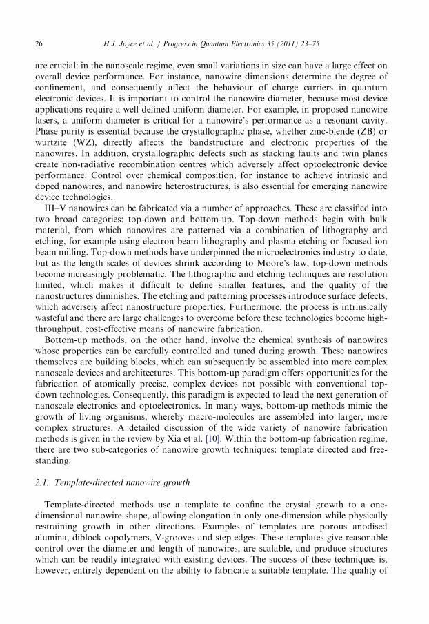
The free-standing nanowire growth method relies on anisotropy of growth rates.Generally, nanowires nucleate at a single point and elongate in the growth direction withthe highest growth rate. The slower growth rates of other directions constrain the nanowireto a one-dimensional shape. Numerous techniques exist for free-standing nanowiregrowth, including self-catalysed growth, oxide-assisted growth, vapour–liquid–solid (VLS)growth [11], and solution–liquid–solid growth [12], to name a few. Nanowires can begrown from a solution or from a vapour phase, and may grow suspended in the growthmedium or grow in contact with a substrate.
The VLS mechanism is the most widely cited growth method. The VLS mechanism wasoriginally proposed by Wagner and Ellis [11] in 1964 to explain the anisotropic growth ofSi wires catalysed by metallic Au particles. The VLS mechanism, so-called due to thevapour, liquid and solid phases involved, is schematically illustrated in Fig. 2.1. The Siprecursor species were supplied in the vapour phase. At growth temperature the metallicAu particle formed a liquid eutectic alloy with the Si. With further supply of Si this Au–Sialloy particle became supersaturated with Si, and the Si precipitated at the particle–semiconductor interface to form a solid crystalline Si wire. Wagner and Ellis proposed twopossibilities to explain nanowire growth. First, that due to the high accommodationcoefficient of the liquid phase, the liquid particles are favourable collection sites for thevapour phase reaction species, and thus assist nanowire growth. The second possibility isthat the metallic particle is a chemical catalyst which lowers the activation energy barriersto enhance the decomposition of the gas-phase precursors [13].
Following work on Si wire growth, Hiruma et al. [14] applied the same principle to growIII–V nanowires. Hiruma et al. [14] used Au nanoparticles to direct III–V nanowire growthvia a VLS-like mechanism. We refer to this nanowire growth process as ‘‘Au-assisted’’, ascoined by Dick et al. [15].
For III–V nanowires, this Au-assisted nanowire growth mechanism lends itself to anumber of standard industrial and laboratory growth systems, including laser-assistedcatalytic growth [16], molecular beam epitaxy (MBE) [17], chemical beam epitaxy (CBE)[18], and metalorganic chemical vapour deposition (MOCVD) [19,20]. Of all thesetechniques, the most promising and most common technique for III–V nanowire growth isMOCVD. This approach achieves epitaxial nanowires that are free-standing on the growthsubstrate, offers great flexibility and high accuracy in nanowire design, and is readilyscalable for industrial mass fabrication. The growth parameters can be tightly controlled toachieve the desired material properties. Indeed, Au-assisted MOCVD growth hasproduced nanowires with abrupt heterostructure interfaces, high purity, controlleddoping, and perfect phase purity. For these reasons, Au-assisted MOCVD is our methodof choice for III–V nanowire device fabrication.
Fig. 2.1. Schematic illustration of the VLS growth of Si wires using an Au catalyst particle. The Au–Si binary
phase diagram illustrated in the lower portion indicates the various phases the Au–Si particle can adopt under
different temperatures and in different composition ranges. The grey arrow, and labels (i), (ii) and (iii) illustrate
the different stages of nanowire growth for a growth temperature of 800 1C, and the corresponding state of the
Au–Si particle.
H.J. Joyce et al. / Progress in Quantum Electronics 35 (2011) 23–7528
3. Fundamental principles of III–V nanowire growth by Au-assisted MOCVD
3.1. Basic growth mechanism
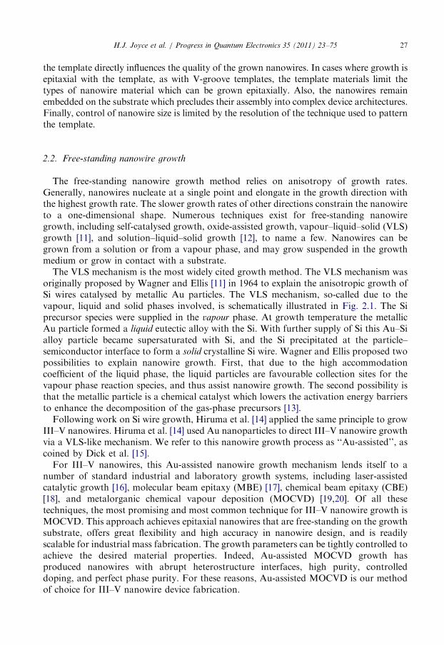
The Au-assisted MOCVD growth mechanism is closely related to, if not identical to, theVLS growth mechanism discussed above. We outline the basic mechanism of III–Vnanowire growth by Au-assisted MOCVD with reference to the schematic illustration ofFig. 3.1. Initially, Au nanoparticles are deposited on a semiconductor substrate surface, asin Fig. 3.1a. To initiate growth, vapour phase group III and group V precursors areprovided to the reaction chamber. During growth, these precursors pyrolyse (decompose)to yield group III and group V elements.Deposition of III–V material occurs preferentially at the nanoparticle–substrate
interface, so that nanowire nucleation takes place (Fig. 3.1c). With continual supply of
Fig. 3.1. Schematic illustration of the nanowire growth mechanism: (a) Au nanoparticles are deposited on the
semiconductor substrate; (b) vapour phase reactants are supplied and the nanoparticle alloys with specific reactant
elements; (c) nucleation takes place at the nanoparticle–substrate interface and (d) growth continues at the
nanoparticle–nanowire interface.
H.J. Joyce et al. / Progress in Quantum Electronics 35 (2011) 23–75 29
group III and V reactants, deposition of III–V material continues at the nanoparticle–nanowire interface. Thus the nanoparticle, located at the growing tip of the nanowire,drives highly anisotropic nanowire growth (Fig. 3.1d). The diameter at the tip of the grownnanowire is governed by the diameter of the Au nanoparticle. The following sectionsdescribe the growth process in further detail. This is essentially a bottom-up fabricationtechnique which offers high controllability in nanoscale dimensions not possible by top-down techniques.
3.2. Growth procedure
In our MOCVD system, group III elements, Ga, In and Al, and group V element, Sb,are supplied as vapour phase organometallic precursor species: trimethylgallium(Ga(CH3)3, TMGa), trimethylindium (In(CH3)3, TMIn), trimethylaluminium (Al(CH3)3,TMAl), and trimethylantimony (Sb(CH3)3, TMSb), respectively. Group V elements Asand P are supplied as vapour phase hydrides: arsine (AsH3) and phosphine (PH3),respectively. These reactants are carried into the reactor by ultra-high purity hydrogen gas,H2. During growth, these precursors pyrolyse to release group III and group V elements.A number of reports describe precursor pyrolysis in detail [21,22].
In our laboratory, (1 1 1)B-oriented III–V substrates, such as GaAs and InP, are usedfor nanowire growth. Typically, nanowires are grown on substrates of the same material,for instance GaAs nanowires are grown on GaAs substrates. Before growth, Aunanoparticles are deposited on the substrate surface, as will be described in Section 5.1.The prepared substrate, hosting deposited Au nanoparticles, is placed into the reactor on agraphite susceptor. The substrate is heated to 600 1C and annealed in situ for 10 min todesorb surface contaminants, including the surface oxide. Annealing is performed undergroup V overpressure to prevent decomposition of the substrate.
After annealing, the substrate is cooled to growth temperature, typically between 350and 550 1C. The group V flow rate is adjusted for growth. Then group III precursors arefed to the reaction chamber to initiate growth. Growth times are generally between 30 sand 120 min, chosen according to the growth rate and the desired nanowire length. Uponcompletion of growth, the samples are cooled under group V overpressure.
H.J. Joyce et al. / Progress in Quantum Electronics 35 (2011) 23–7530
All samples were grown with a reactor pressure of 100 mbar and a total gas flow rateof 15 standard L/min.
3.3. Alloying of the Au nanoparticle
During the annealing and growth processes, the Au nanoparticle alloys with specificgroup III and group V elements to form a liquid or solid alloy, for instance Au–Ga(Fig. 3.1b). The alloying behaviour is significantly more complex than for Au-assisted Siwires (as described in Section 2.2), because at least three different elements are involved:Au, a group III and a group V. Binary and ternary phase diagrams [23–32] indicate whichalloy phases are stable at room temperature, during annealing and at growth temperature.At typical nanowire growth temperatures (between 350 and 550 1C), Al, Ga, In and Sb caneach alloy with Au to produce eutectic liquid or stable solid alloys [23–27]. On the otherhand, P and As are not thought to alloy significantly: the Au–As phase diagram does notinclude any intermetallic solid phases, the only solid Au–P phase is metastable, thesolubility of As and P in solid Au is low, and typical nanowire growth temperatures are toolow to form eutectic liquid Au–As or Au–P alloys [28,29]. Dick et al. [33] have published athorough account of the possible alloy phases of the nanoparticle during growth.Even with the assistance of binary and ternary phase diagrams, it is difficult to ascertain
the exact phase, solid or liquid, of the nanoparticle during growth. Firstly, most phasediagrams were derived for atmospheric pressure rather than the low reactor pressurestypically used for nanowire growth. Secondly, size-dependent melting effects limit theapplicability of bulk phase diagrams. The small scale of the alloyed Au nanoparticlesmakes them subject to size-dependent melting effects, according to the Gibbs–Thomsonrelation. Therefore, the melting point of the alloy nanoparticles may be depressed relativeto the bulk melting point, so eutectic melting may occur at a lower temperature than thebulk phase diagrams predict. A further factor is melting–freezing hysteresis observed foralloyed nanoparticles [34,35].Thirdly, the composition of the particle, when analysed post-growth, is generally different
to that during growth. After growth is complete, the group III flow is ceased and the sample iscooled under group V overpressure. This high group V vapour supersaturation continues todrive the III–V growth reaction which consumes group III species alloyed within thenanoparticle. Thus during cooling, III–V material continues to deposit at the nanoparticle–nanowire interface and group III species in the Au particle are depleted. Several studies havecompared the nanoparticle composition after different cooling procedures, to determine thenanoparticle phase during growth [36,37].Doubt about the physical state of the particle, whether liquid or solid, has created doubt
about whether the growth mechanism is truly VLS. A vapour–solid–solid (VSS) mechanismin which the nanoparticle is solid, has been proposed [15,36,38]. In situ TEM growth studieshave observed both VLS and VSS mechanisms, and have demonstrated that growth is morerapid when the nanoparticle is liquid [39]. According to the conventional VLS and VSSmechanisms, reaction species dissolve into the nanoparticle and are transported to thegrowth interface via bulk diffusion through the nanoparticle. The elements with highsolubility in Au (Al, Ga, In, Sb) are assumed to travel to the interface by bulk diffusionthrough the nanoparticle, whereas the elements with low solubility (As, P) are thought toarrive at the growth interface directly from the vapour, without dissolving into thenanoparticle. In this case, As and P would be incorporated at the three phase contact line
H.J. Joyce et al. / Progress in Quantum Electronics 35 (2011) 23–75 31
where vapour, nanoparticle and nanowire meet. Another strong possibility is that reactantsare transported to the growth interface by diffusing on the nanoparticle surface, rather thanby diffusing through the nanoparticle interior [40].
Recently, the theory of preferential interface nucleation (PIN) has been proposed as thefundamental mechanism underpinning the VLS mechanism and variations such as the VSSmechanism and the solution–liquid–solid mechanism [41]. According to the PIN theory,the probability of nucleation is highest at the nanoparticle–semiconductor interface andthis drives nanowire growth. A comprehensive review article by Dick [22] describes recentprogress towards understanding the mechanism of Au-assisted nanowire growth.
Despite these controversies, the general principle of Au-assisted nanowire growthremains: the nucleation rate is highest at the Au nanoparticle–semiconductor interface,which drives nanowire growth.
3.4. Axial and radial growth modes
There are two major growth modes taking place during Au-assisted nanowire growth byMOCVD: axial growth and radial growth.
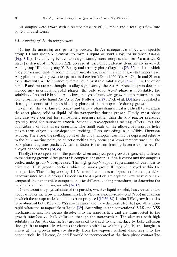
Axial growth is the term describing the Au-assisted elongating growth of the nanowire.There are two major contributions to axial nanowire growth, as illustrated in Fig. 3.2a.The first contribution is from reaction species which directly impinge on the nanoparticle.The second contribution arises from species adsorbed on the substrate or nanowiresidewalls. These adatoms (adsorbed atoms) diffuse along the concentration gradienttowards the Au nanoparticle, where they are incorporated into axial growth. Surfacediffusion is more significant for group III adatoms, which have large diffusion lengths (l),
Fig. 3.2. Schematic illustration of adatom contributions to (a) axial growth and (b) radial growth. The adatom
contributions include those (1) directly impinging on the Au nanoparticle and those adsorbed on the (2) substrate
and (3) nanowire sidewalls which (4) diffuse along the concentration gradient towards the nanoparticle–nanowire
interface.
H.J. Joyce et al. / Progress in Quantum Electronics 35 (2011) 23–7532
whereas group V adatoms have much smaller diffusion lengths. Group V species havesignificantly lower diffusivity, and are believed to incorporate close to the position ofadsorption.Johansson et al. [42] have developed a theoretical model describing the dependence
of the axial growth rate on the diffusion length on the substrate (ls) and nanowiresidewalls (lw). The diffusion of adatoms gives rise to some interesting nanowire growthresults. One of these results is density dependence. In regions of high nanowire density,adjacent nanowires spaced within a diffusion length, ls, compete for diffusing adatoms.As a result, nanowires in high density regions may feature slower axial growth rates thanthose in low density regions [43]. Another report by Dayeh et al. [44] describes twodifferent growth regimes, defined by whether ls or lw is larger, which lead to time-varyinggrowth rates.Radial growth, also known as lateral or conformal growth, is the deposition of material
on the nanowire sidewalls. It follows a simple vapour–solid growth mechanism, and doesnot directly involve the Au nanoparticle. As illustrated in Fig. 3.2b, radial growth occurswhen species adsorbed on the substrate and nanowire sidewalls, diffuse and incorporate onthe nanowire sidewalls. In this manner, radial growth competes with axial growth.Tapered nanowire morphologies, whereby nanowires exhibit wider bases and taper to
narrower Au-capped tips, are a consequence of radial growth, as explained here. Nanowirebases are grown first, and hence are exposed to reactants for longer than the more recentlygrown Au nanoparticle-capped tip. Also, owing to their proximity to the substrate, thenanowire bases receive a greater fraction of precursor materials collected on and diffusingfrom the substrate [45]. Thus, lower sections of the nanowire experience more radialgrowth, which leads to tapered nanowire morphologies with wider bases and narrower tipsas illustrated in Fig. 3.2b.A further growth process is the deposition of planar layers on the substrate surface. This
occurs when adatoms incorporate onto the substrate, rather than onto the nanowiresidewalls or nanowire tip.
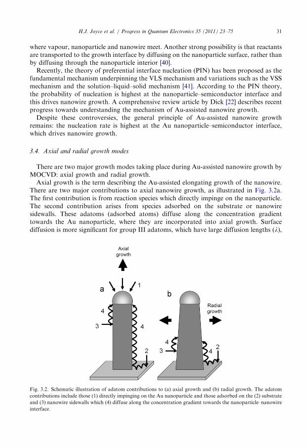
4. Nanowire morphology and crystal structure
Field emission scanning electron microscopy (FESEM) is used to identify generalnanowire morphology, including facet planes, diameter and height. Typically, theFESEM is operated at low acceleration voltages, generally 3 kV. In Fig. 4.1a and b, weillustrate FESEM images of typical GaAs and InAs nanowires grown via Au-assistedMOCVD. The nanowires are vertically aligned on their (1 1 1)B terminated substratesindicating their epitaxial relationship with the substrate. The [1 1 1]B direction is theenergetically preferred growth direction. These nanowires are tapered with narrow tips andwider bases. At the tip of each nanowire lies an Au alloy nanoparticle which drivesnanowire growth.
4.1. Nanowire crystal structure
Transmission electron microscopy (TEM) is used to determine crystallographicproperties and further elucidate nanowire structure. III–V nanowires can adopt either acubic zinc-blende (ZB) structure or hexagonal wurtzite (WZ) structure. The WZ structurehas been reported, for instance, in MOCVD-grown InP nanowires [46] and in MBE-grown
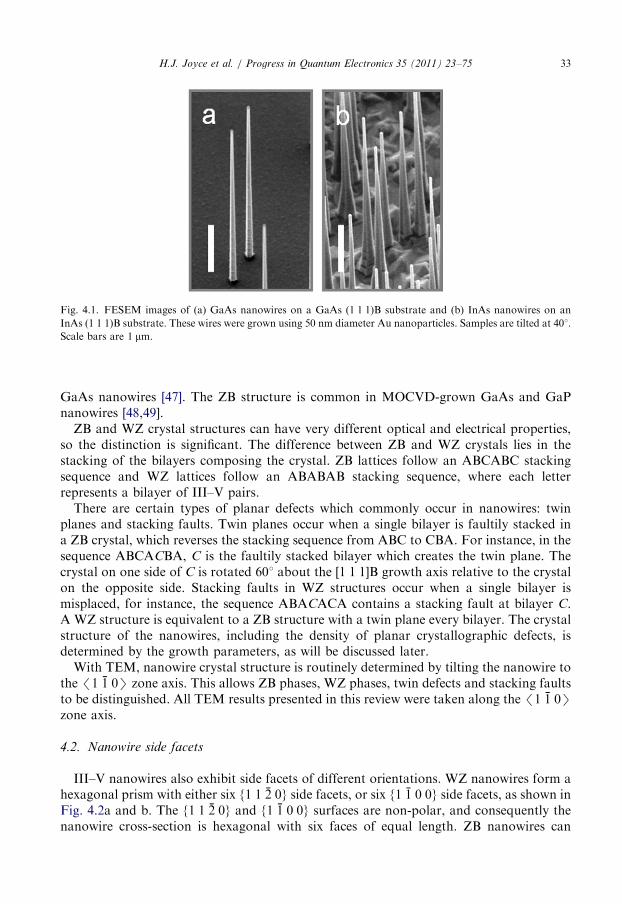
Fig. 4.1. FESEM images of (a) GaAs nanowires on a GaAs (1 1 1)B substrate and (b) InAs nanowires on an
InAs (1 1 1)B substrate. These wires were grown using 50 nm diameter Au nanoparticles. Samples are tilted at 401.
Scale bars are 1 mm.
H.J. Joyce et al. / Progress in Quantum Electronics 35 (2011) 23–75 33
GaAs nanowires [47]. The ZB structure is common in MOCVD-grown GaAs and GaPnanowires [48,49].
ZB and WZ crystal structures can have very different optical and electrical properties,so the distinction is significant. The difference between ZB and WZ crystals lies in thestacking of the bilayers composing the crystal. ZB lattices follow an ABCABC stackingsequence and WZ lattices follow an ABABAB stacking sequence, where each letterrepresents a bilayer of III–V pairs.
There are certain types of planar defects which commonly occur in nanowires: twinplanes and stacking faults. Twin planes occur when a single bilayer is faultily stacked ina ZB crystal, which reverses the stacking sequence from ABC to CBA. For instance, in thesequence ABCACBA, C is the faultily stacked bilayer which creates the twin plane. Thecrystal on one side of C is rotated 601 about the [1 1 1]B growth axis relative to the crystalon the opposite side. Stacking faults in WZ structures occur when a single bilayer ismisplaced, for instance, the sequence ABACACA contains a stacking fault at bilayer C.A WZ structure is equivalent to a ZB structure with a twin plane every bilayer. The crystalstructure of the nanowires, including the density of planar crystallographic defects, isdetermined by the growth parameters, as will be discussed later.
With TEM, nanowire crystal structure is routinely determined by tilting the nanowire tothe /1 1 0S zone axis. This allows ZB phases, WZ phases, twin defects and stacking faultsto be distinguished. All TEM results presented in this review were taken along the /1 1 0Szone axis.
4.2. Nanowire side facets
III–V nanowires also exhibit side facets of different orientations. WZ nanowires form ahexagonal prism with either six {1 1 2 0} side facets, or six {1 1 0 0} side facets, as shown inFig. 4.2a and b. The {1 1 2 0} and {1 1 0 0} surfaces are non-polar, and consequently thenanowire cross-section is hexagonal with six faces of equal length. ZB nanowires can
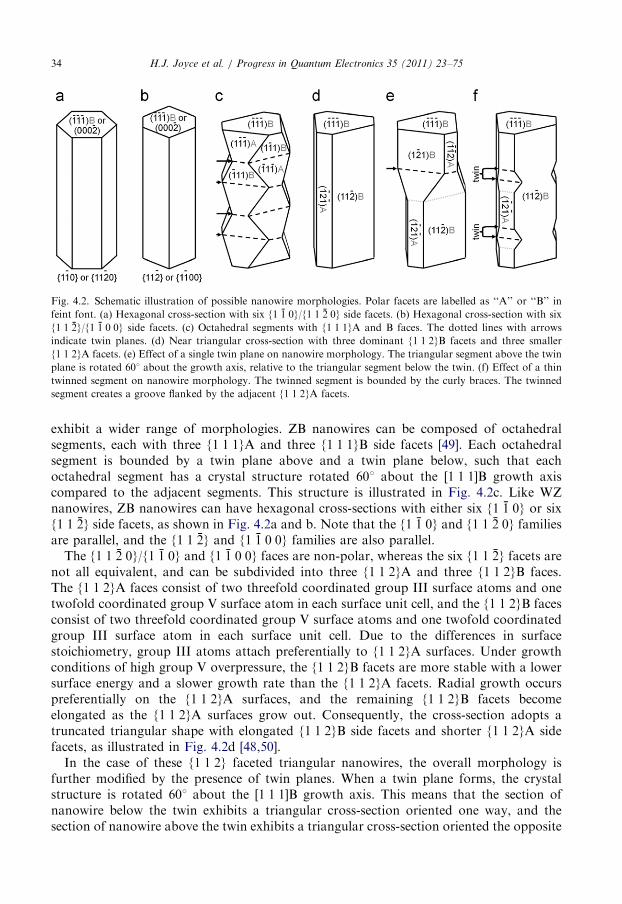
Fig. 4.2. Schematic illustration of possible nanowire morphologies. Polar facets are labelled as ‘‘A’’ or ‘‘B’’ in
feint font. (a) Hexagonal cross-section with six {1 1 0}/{1 1 2 0} side facets. (b) Hexagonal cross-section with six
{1 1 2}/{1 1 0 0} side facets. (c) Octahedral segments with {1 1 1}A and B faces. The dotted lines with arrows
indicate twin planes. (d) Near triangular cross-section with three dominant {1 1 2}B facets and three smaller
{1 1 2}A facets. (e) Effect of a single twin plane on nanowire morphology. The triangular segment above the twin
plane is rotated 601 about the growth axis, relative to the triangular segment below the twin. (f) Effect of a thin
twinned segment on nanowire morphology. The twinned segment is bounded by the curly braces. The twinned
segment creates a groove flanked by the adjacent {1 1 2}A facets.
H.J. Joyce et al. / Progress in Quantum Electronics 35 (2011) 23–7534
exhibit a wider range of morphologies. ZB nanowires can be composed of octahedralsegments, each with three {1 1 1}A and three {1 1 1}B side facets [49]. Each octahedralsegment is bounded by a twin plane above and a twin plane below, such that eachoctahedral segment has a crystal structure rotated 601 about the [1 1 1]B growth axiscompared to the adjacent segments. This structure is illustrated in Fig. 4.2c. Like WZnanowires, ZB nanowires can have hexagonal cross-sections with either six {1 1 0} or six{1 1 2} side facets, as shown in Fig. 4.2a and b. Note that the {1 1 0} and {1 1 2 0} familiesare parallel, and the {1 1 2} and {1 1 0 0} families are also parallel.The {1 1 2 0}/{1 1 0} and {1 1 0 0} faces are non-polar, whereas the six {1 1 2} facets are
not all equivalent, and can be subdivided into three {1 1 2}A and three {1 1 2}B faces.The {1 1 2}A faces consist of two threefold coordinated group III surface atoms and onetwofold coordinated group V surface atom in each surface unit cell, and the {1 1 2}B facesconsist of two threefold coordinated group V surface atoms and one twofold coordinatedgroup III surface atom in each surface unit cell. Due to the differences in surfacestoichiometry, group III atoms attach preferentially to {1 1 2}A surfaces. Under growthconditions of high group V overpressure, the {1 1 2}B facets are more stable with a lowersurface energy and a slower growth rate than the {1 1 2}A facets. Radial growth occurspreferentially on the {1 1 2}A surfaces, and the remaining {1 1 2}B facets becomeelongated as the {1 1 2}A surfaces grow out. Consequently, the cross-section adopts atruncated triangular shape with elongated {1 1 2}B side facets and shorter {1 1 2}A sidefacets, as illustrated in Fig. 4.2d [48,50].In the case of these {1 1 2} faceted triangular nanowires, the overall morphology is
further modified by the presence of twin planes. When a twin plane forms, the crystalstructure is rotated 601 about the [1 1 1]B growth axis. This means that the section ofnanowire below the twin exhibits a triangular cross-section oriented one way, and thesection of nanowire above the twin exhibits a triangular cross-section oriented the opposite
H.J. Joyce et al. / Progress in Quantum Electronics 35 (2011) 23–75 35
way, as illustrated in Fig. 4.2e. Finally, if a thin twinned segment is inserted into a perfectcrystal region, it creates a groove between the {1 1 2}A sidewalls flanking the twinnedsegment, as illustrated in Fig. 4.2f. The groove forms there, because there the twinnedsegment presents a slow-growing {1 1 2}B sidewall, not a {1 1 2}A sidewall like thoseflanking the twinned segment. As a result the nanowire structure resembles a stack oftruncated triangles [48].
The above discussion has focused the formation of elongated {1 1 2}B facets under highgroup V overpressure. Under growth conditions of low group V overpressure, the situationcan reverse so that {1 1 2}A facets become more elongated [50].
5. Tailoring nanowire growth
In MOCVD, a number of growth parameters can be accurately tuned to grow highquality nanowires suitable for device applications. To a first approximation, the diameter
at the tip of the nanowire is determined by the catalyst diameter. Other nanowireproperties, such as height, morphology, crystal structure, crystallographic defects andimpurity incorporation can be tailored by choosing appropriate growth parameters. Theseinclude growth time, temperature, pressure and the flow rates of group III and group Vprecursors [51–53].
The focus of this section is tailoring the MOCVD growth of III–V nanowires, usingGaAs nanowires as the primary example. The GaAs nanowires presented in this sectionwere grown on GaAs (1 1 1)B substrates using TMGa and AsH3 precursors.
5.1. Substrate preparation
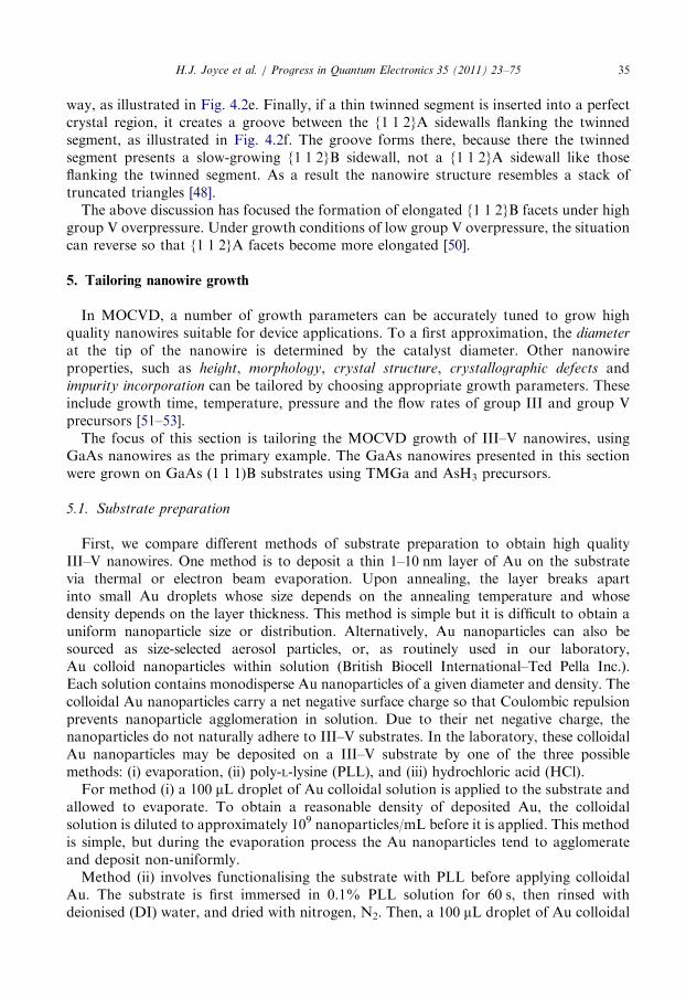
First, we compare different methods of substrate preparation to obtain high qualityIII–V nanowires. One method is to deposit a thin 1–10 nm layer of Au on the substratevia thermal or electron beam evaporation. Upon annealing, the layer breaks apartinto small Au droplets whose size depends on the annealing temperature and whosedensity depends on the layer thickness. This method is simple but it is difficult to obtain auniform nanoparticle size or distribution. Alternatively, Au nanoparticles can also besourced as size-selected aerosol particles, or, as routinely used in our laboratory,Au colloid nanoparticles within solution (British Biocell International–Ted Pella Inc.).Each solution contains monodisperse Au nanoparticles of a given diameter and density. Thecolloidal Au nanoparticles carry a net negative surface charge so that Coulombic repulsionprevents nanoparticle agglomeration in solution. Due to their net negative charge, thenanoparticles do not naturally adhere to III–V substrates. In the laboratory, these colloidalAu nanoparticles may be deposited on a III–V substrate by one of the three possiblemethods: (i) evaporation, (ii) poly-L-lysine (PLL), and (iii) hydrochloric acid (HCl).
For method (i) a 100 mL droplet of Au colloidal solution is applied to the substrate andallowed to evaporate. To obtain a reasonable density of deposited Au, the colloidalsolution is diluted to approximately 109 nanoparticles/mL before it is applied. This methodis simple, but during the evaporation process the Au nanoparticles tend to agglomerateand deposit non-uniformly.
Method (ii) involves functionalising the substrate with PLL before applying colloidalAu. The substrate is first immersed in 0.1% PLL solution for 60 s, then rinsed withdeionised (DI) water, and dried with nitrogen, N2. Then, a 100 mL droplet of Au colloidal
H.J. Joyce et al. / Progress in Quantum Electronics 35 (2011) 23–7536
solution is dispersed on the substrate, and rinsed away with DI water after a contact timeof 5–30 s, and the substrate is again dried with N2. A longer contact time is used for lowerdensity Au colloidal solutions, to achieve a sufficient density of Au nanoparticles adheringto the substrate surface. PLL is a positively charged polyelectrolyte which attracts thenegatively charged Au nanoparticles and immobilises them on the substrate surface. ThisPLL functionalisation–Au nanoparticle deposition method prevents agglomeration ofnanoparticles during deposition and achieves an even distribution on the substrate.Treatment with polyamines, such as PLL, is widely used in the life sciences to immobilisecells on slides, and also has been used to immobilise nanoparticles to create standardsamples for atomic force microscope calibration [54]. The resulting nanowires are shown inFig. 5.1a.Method (iii) involves dispensing a 100 mL droplet of Au colloidal solution on the
substrate. Then, a 50 mL droplet of 0.03 M HCl is added to the Au colloid droplet andallowed to mix on the substrate for 10 s. The resulting HCl concentration is 0.01 M. Thesubstrate is rinsed with DI water and dried with N2. This method was developed byWoodruff et al. [55] for deposition of Au colloids on Si substrates using HF insteadof HCl. When the acid is added to the Au colloid droplet, the droplet pH is lowered,the negative charge on the Au nanoparticles is neutralised, and the nanoparticles canattach to the substrates. Fig. 5.1b shows nanowires grown on substrates prepared by thismethod.The optimum method, which affords control over both nanoparticle size and
distribution, is patterning of Au nanoparticles using electron beam lithography (EBL).This technique is time-consuming and requires complex EBL processing. The PLLfunctionalisation–Au colloid deposition process, used routinely in this work, is suitable formost device applications and is ideal for research into nanowire growth processes. It issuitable for all substrates used, including III–V substrates and the quartz substrates used
Fig. 5.1. FESEM images of GaAs nanowires grown on GaAs substrates prepared by different methods:
(a) substrate prepared by the PLL method (method (ii)), involving PLL functionalisation followed by colloidal Au
deposition, followed by an in situ annealing step prior to nanowire growth; (b) substrate prepared by the HCl
method (method (iii)), involving deposition of HCl and Au colloidal solutions, followed by an in situ annealing
step prior to nanowire growth; (c) substrate prepared using the PLL (method (ii)) but without any in situ
annealing step; (d) substrate prepared using the HCl (method (iii)) but without any in situ annealing step and
(e) substrate etched in 1 M HCl, prior to treatment with the HCl method (method (iii)). Scale bar is 1 mm.
H.J. Joyce et al. / Progress in Quantum Electronics 35 (2011) 23–75 37
for TCS measurements. Unless otherwise stated, all samples presented in this article wereprepared using PLL functionalisation, followed by Au colloid deposition.
Before growth, the substrates are annealed in situ, as described in Section 3.2. Theannealing step removes the surface oxide and other contaminants. In Fig. 5.1 the effect ofthe annealing step is clear from comparing parts a and b, where growth was performedwith a pre-growth annealing, against parts c and d, where growth was performed withouta pre-growth annealing step. Nanowire growth is more irregular in parts c and d,presumably because surface roughness and contaminants remaining on the unannealedsurface hinder the nucleation of straight epitaxial nanowires. The similarity between thePLL and HCl treated samples indicates that PLL functionalisation does not interferesignificantly with nanowire growth. PLL and HCl treatments were also compared for InAssubstrates with InAs nanowires, and the two treatments gave identical results.
This annealing step means that the III–V substrates do not require etching or cleaningbefore growth. Etching to remove the surface oxide, prior to Au nanoparticle deposition,was performed for the sample of Fig. 5.1e. To etch the substrate, it was immersed in1 M HCl for 2 min, rinsed with DI water and dried with N2. We found that etching did nothave any measurable effect on the properties of the grown nanowires. As seen in Fig. 5.1by comparing part a (or b) with part e, the resulting nanowire properties are comparableregardless of etching.
5.2. Effects of growth temperature
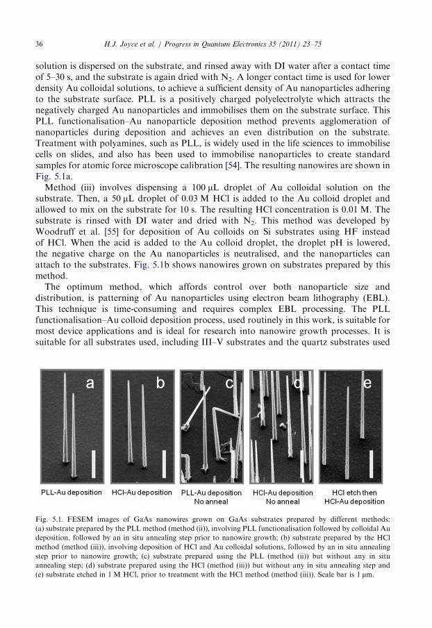
Growth temperature has a marked effect on nanowire properties. Fig. 5.2 illustrates themorphological changes that take place with different growth temperatures. In Fig. 5.2aand b, we note that temperature increases both axial and radial growth rates, so thatnanowires are taller and have wider bases. This occurs because, as temperature isincreased, the rate of precursor decomposition increases and the adatom diffusion lengthincreases. More Ga adatoms are available for both axial and radial growth.
As temperature is increased beyond 450 1C (Fig. 5.2b and c), however, only the radialand planar growth rates continue to increase and the axial growth rate decreases. Thisoccurs because the increasing radial growth and planar growth compete with axial growth
Fig. 5.2. FESEM images of GaAs nanowires grown at growth temperatures of: (a) 425 1C, (b) 450 1C and
(c) 475 1C. Samples are tilted at 401. Scale bar is 1 mm.
H.J. Joyce et al. / Progress in Quantum Electronics 35 (2011) 23–7538
for diffusing adatoms. This competing growth depletes the nanoparticle–nanowireinterface of Ga adatoms diffusing from the substrate and along nanowire sidewalls, andconsequently axial growth decreases. Consequently, at the highest growth temperatures(Fig. 5.2c), the nanowires are short and suffer severe tapering.Tapering is undesirable for many device applications, including lasers, where a uniform
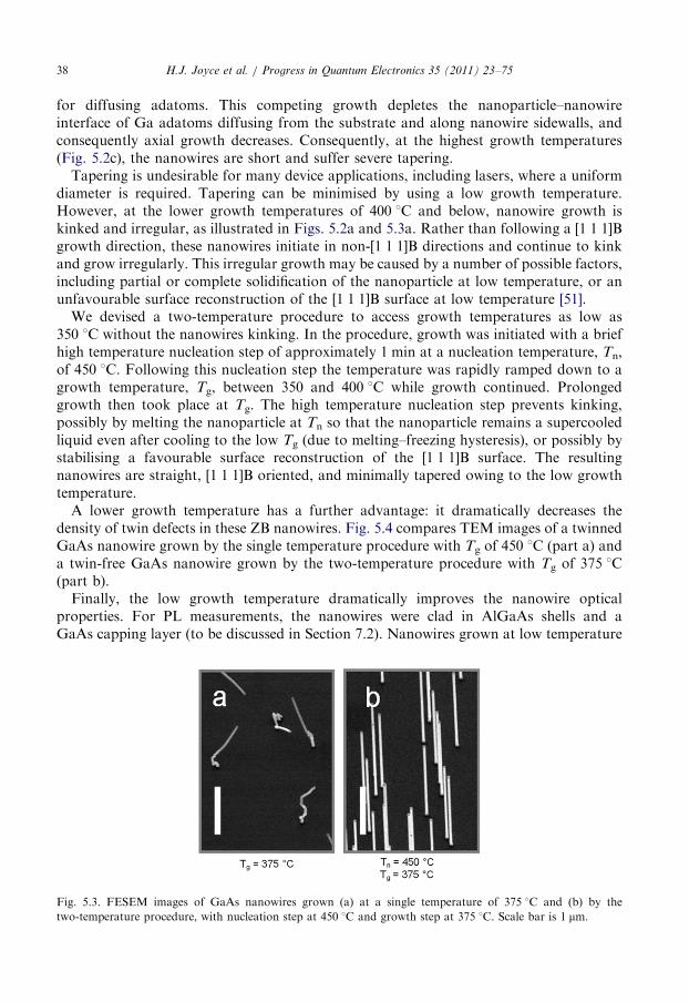
diameter is required. Tapering can be minimised by using a low growth temperature.However, at the lower growth temperatures of 400 1C and below, nanowire growth iskinked and irregular, as illustrated in Figs. 5.2a and 5.3a. Rather than following a [1 1 1]Bgrowth direction, these nanowires initiate in non-[1 1 1]B directions and continue to kinkand grow irregularly. This irregular growth may be caused by a number of possible factors,including partial or complete solidification of the nanoparticle at low temperature, or anunfavourable surface reconstruction of the [1 1 1]B surface at low temperature [51].We devised a two-temperature procedure to access growth temperatures as low as
350 1C without the nanowires kinking. In the procedure, growth was initiated with a briefhigh temperature nucleation step of approximately 1 min at a nucleation temperature, Tn,of 450 1C. Following this nucleation step the temperature was rapidly ramped down to agrowth temperature, Tg, between 350 and 400 1C while growth continued. Prolongedgrowth then took place at Tg. The high temperature nucleation step prevents kinking,possibly by melting the nanoparticle at Tn so that the nanoparticle remains a supercooledliquid even after cooling to the low Tg (due to melting–freezing hysteresis), or possibly bystabilising a favourable surface reconstruction of the [1 1 1]B surface. The resultingnanowires are straight, [1 1 1]B oriented, and minimally tapered owing to the low growthtemperature.A lower growth temperature has a further advantage: it dramatically decreases the
density of twin defects in these ZB nanowires. Fig. 5.4 compares TEM images of a twinnedGaAs nanowire grown by the single temperature procedure with Tg of 450 1C (part a) anda twin-free GaAs nanowire grown by the two-temperature procedure with Tg of 375 1C(part b).Finally, the low growth temperature dramatically improves the nanowire optical
properties. For PL measurements, the nanowires were clad in AlGaAs shells and aGaAs capping layer (to be discussed in Section 7.2). Nanowires grown at low temperature
Fig. 5.3. FESEM images of GaAs nanowires grown (a) at a single temperature of 375 1C and (b) by the
two-temperature procedure, with nucleation step at 450 1C and growth step at 375 1C. Scale bar is 1 mm.
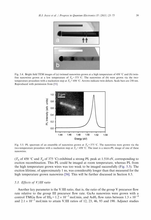
Fig. 5.4. Bright field TEM images of (a) twinned nanowires grown at a high temperature of 450 1C and (b) twin-
free nanowires grown at a low temperature of Tg=375 1C. The nanowires of (b) were grown via the two-
temperature procedure with a nucleation step at Tn=450 1C. Arrows indicate twin defects. Scale bars are 250 nm.
Reproduced with permission from [51].
Fig. 5.5. PL spectrum of an ensemble of nanowires grown at Tg=375 1C. The nanowires were grown via the
two-temperature procedure with a nucleation step at Tn=450 1C. The inset is a micro-PL image of one of these
nanowires.
H.J. Joyce et al. / Progress in Quantum Electronics 35 (2011) 23–75 39
(Tn of 450 1C and Tg of 375 1C) exhibited a strong PL peak at 1.518 eV, corresponding toexciton recombination. This PL could be imaged at room temperature, whereas PL fromthe high temperature grown wires was too weak to be imaged successfully (Fig. 5.5). Theexciton lifetime, of approximately 1 ns, was considerably longer than that measured for thehigh temperature grown nanowires [56]. This will be further discussed in Section 8.5.
5.3. Effects of V/III ratio
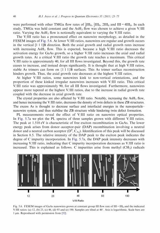
Another key parameter is the V/III ratio, that is, the ratio of the group V precursor flowrate relative to the group III precursor flow rate. GaAs nanowires were grown with acontrol TMGa flow of III0=1.2� 10�5 mol/min, and AsH3 flow rates between 1.3� 10�4
and 2.1� 10�3 mol/min to attain V/III ratios of 12, 23, 46, 93 and 190. Adjunct studies
H.J. Joyce et al. / Progress in Quantum Electronics 35 (2011) 23–7540
were performed with other TMGa flow rates of 14III0,
12III0, 2III0 and III=4III0. In each
study, TMGa was held constant and the AsH3 flow was chosen to achieve a given V/IIIratio. Varying the AsH3 flow is notionally equivalent to varying the V/III ratio.The V/III ratio has a pronounced effect on nanowire morphology, as detailed in the
FESEM images of Fig. 5.6. At lower V/III ratios, nanowires are regular and growth occursin the vertical [1 1 1]B direction. Both the axial growth and radial growth rates increasewith increasing AsH3 flow. This is expected, because a high V/III ratio decreases theactivation energy for GaAs growth, so a higher V/III ratio increases the axial and radialgrowth rates. At a critical V/III ratio the growth rate reaches a maximum. This criticalV/III ratio is approximately 40, for all III flows investigated. Beyond this, the growth rateceases to increase, and instead drops significantly. It is thought that at high V/III ratios,stable As trimers can form on {1 1 1}B surfaces. This As trimer surface reconstructionhinders growth. Thus, the axial growth rate decreases at the highest V/III ratios.At higher V/III ratios, some nanowires kink to non-vertical orientations, and the
proportion of these kinked irregular nanowires increases with V/III ratio. This criticalV/III ratio was approximately 90, for all III flows investigated. Furthermore, nanowiresappear more tapered at the highest V/III ratios, due to the increase in radial growth ratecoupled with the decrease in axial growth rate.The crystal properties are also affected by V/III ratio. Notably, increasing the AsH3 flow,
and hence increasing the V/III ratio, decreases the density of twin defects in these ZB structures.The excess As is thought to decrease surface and interfacial energies in the nanoparticle–nanowire system, and thus stabilise the ZB structure while hindering twin defect formation.PL measurements reveal the effect of V/III ratio on nanowire optical properties.
In Fig. 5.7a we plot the PL spectra of three samples grown with different V/III ratios.The peak at 1.518 eV is characteristic of free exciton recombination in GaAs. The lowerenergy peak arises from donor–acceptor-pair (DAP) recombination involving a neutraldonor and a neutral carbon acceptor (D0, CAs). Identification of this peak will be discussedin Section 8.5. The relative intensity of the DAP peak to the exciton peak indicates thedegree of C impurity incorporation. In Fig. 5.7a, the DAP peak intensity decreases withincreasing V/III ratio, indicating that C impurity incorporation decreases as V/III ratio isincreased. This is explained as follows. C impurities arise from methyl (CH3) radicals
Fig. 5.6. FESEM images of GaAs nanowires grown at constant group III flow rate of III=III0 and the indicated
V/III ratios: (a) 12, (b) 23, (c) 46, (d) 93 and (e) 190. Samples are tilted at 401. Axis is logarithmic. Scale bars are
1 mm. Reproduced with permission from [52].
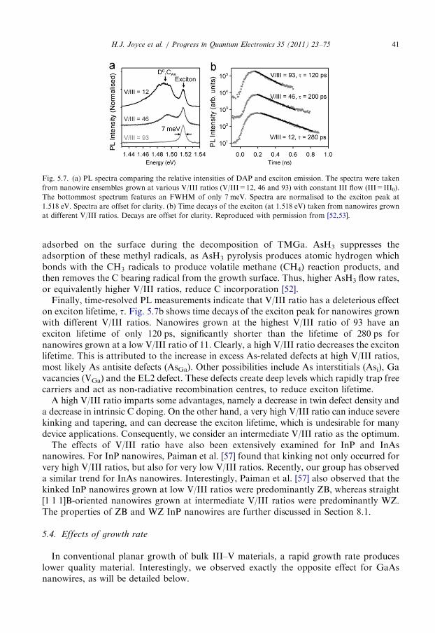
Fig. 5.7. (a) PL spectra comparing the relative intensities of DAP and exciton emission. The spectra were taken
from nanowire ensembles grown at various V/III ratios (V/III=12, 46 and 93) with constant III flow (III=III0).
The bottommost spectrum features an FWHM of only 7 meV. Spectra are normalised to the exciton peak at
1.518 eV. Spectra are offset for clarity. (b) Time decays of the exciton (at 1.518 eV) taken from nanowires grown
at different V/III ratios. Decays are offset for clarity. Reproduced with permission from [52,53].
H.J. Joyce et al. / Progress in Quantum Electronics 35 (2011) 23–75 41
adsorbed on the surface during the decomposition of TMGa. AsH3 suppresses theadsorption of these methyl radicals, as AsH3 pyrolysis produces atomic hydrogen whichbonds with the CH3 radicals to produce volatile methane (CH4) reaction products, andthen removes the C bearing radical from the growth surface. Thus, higher AsH3 flow rates,or equivalently higher V/III ratios, reduce C incorporation [52].
Finally, time-resolved PL measurements indicate that V/III ratio has a deleterious effecton exciton lifetime, t. Fig. 5.7b shows time decays of the exciton peak for nanowires grownwith different V/III ratios. Nanowires grown at the highest V/III ratio of 93 have anexciton lifetime of only 120 ps, significantly shorter than the lifetime of 280 ps fornanowires grown at a low V/III ratio of 11. Clearly, a high V/III ratio decreases the excitonlifetime. This is attributed to the increase in excess As-related defects at high V/III ratios,most likely As antisite defects (AsGa). Other possibilities include As interstitials (Asi), Gavacancies (VGa) and the EL2 defect. These defects create deep levels which rapidly trap freecarriers and act as non-radiative recombination centres, to reduce exciton lifetime.
A high V/III ratio imparts some advantages, namely a decrease in twin defect density anda decrease in intrinsic C doping. On the other hand, a very high V/III ratio can induce severekinking and tapering, and can decrease the exciton lifetime, which is undesirable for manydevice applications. Consequently, we consider an intermediate V/III ratio as the optimum.
The effects of V/III ratio have also been extensively examined for InP and InAsnanowires. For InP nanowires, Paiman et al. [57] found that kinking not only occurred forvery high V/III ratios, but also for very low V/III ratios. Recently, our group has observeda similar trend for InAs nanowires. Interestingly, Paiman et al. [57] also observed that thekinked InP nanowires grown at low V/III ratios were predominantly ZB, whereas straight[1 1 1]B-oriented nanowires grown at intermediate V/III ratios were predominantly WZ.The properties of ZB and WZ InP nanowires are further discussed in Section 8.1.
5.4. Effects of growth rate
In conventional planar growth of bulk III–V materials, a rapid growth rate produceslower quality material. Interestingly, we observed exactly the opposite effect for GaAsnanowires, as will be detailed below.
H.J. Joyce et al. / Progress in Quantum Electronics 35 (2011) 23–7542
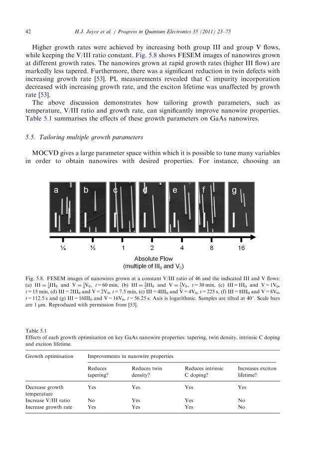
Higher growth rates were achieved by increasing both group III and group V flows,while keeping the V/III ratio constant. Fig. 5.8 shows FESEM images of nanowires grownat different growth rates. The nanowires grown at rapid growth rates (higher III flow) aremarkedly less tapered. Furthermore, there was a significant reduction in twin defects withincreasing growth rate [53]. PL measurements revealed that C impurity incorporationdecreased with increasing growth rate, and the exciton lifetime was unaffected by growthrate [53].The above discussion demonstrates how tailoring growth parameters, such as
temperature, V/III ratio and growth rate, can significantly improve nanowire properties.Table 5.1 summarises the effects of these growth parameters on GaAs nanowires.
5.5. Tailoring multiple growth parameters
MOCVD gives a large parameter space within which it is possible to tune many variablesin order to obtain nanowires with desired properties. For instance, choosing an
Fig. 5.8. FESEM images of nanowires grown at a constant V/III ratio of 46 and the indicated III and V flows:
(a) III ¼ 14III0 and V ¼ 1
4V0, t=60 min, (b) III ¼ 1
2III0 and V ¼ 1
2V0, t=30 min, (c) III=III0 and V=1V0,
t=15 min, (d) III=2III0 and V=2V0, t=7.5 min, (e) III=4III0 and V=4V0, t=225 s, (f) III=8III0 and V=8V0,
t=112.5 s and (g) III=16III0 and V=16V0, t=56.25 s. Axis is logarithmic. Samples are tilted at 401. Scale bars
are 1 mm. Reproduced with permission from [53].
Table 5.1
Effects of each growth optimisation on key GaAs nanowire properties: tapering, twin density, intrinsic C doping
and exciton lifetime.
Growth optimisation Improvements in nanowire properties
Reduces
tapering?
Reduces twin
density?
Reduces intrinsic
C doping?
Increases exciton
lifetime?
Decrease growth
temperature
Yes Yes Yes Yes
Increase V/III ratio No Yes Yes No
Increase growth rate Yes Yes Yes No
H.J. Joyce et al. / Progress in Quantum Electronics 35 (2011) 23–75 43
appropriate growth temperature coupled with an appropriate V/III ratio can affordvery precise control over nanowire properties. Recently, we succeeded in growingGaAs nanowires with a pure WZ structure, simply by using a high temperature coupledwith a low V/III ratio [58]. These nanowires were completely free of stacking faults.Conversely, twin-free zinc-blende nanowires could be obtained simply by using alow temperature coupled with a high V/III ratio, as already discussed in Sections 5.2and 5.3.
These principles were readily extended to InAs nanowires. Twin-free ZB InAs nanowireswere grown using a low temperature and high V/III ratio, whereas stacking fault-free WZInAs nanowires were grown using a high temperature and low V/III ratio [58].
A final parameter of interest is the nanowire diameter. Paiman et al. [57] observed forInP nanowires that smaller diameters adopt a WZ structure whereas larger diametersadopt a ZB structure. By tailoring both V/III ratio and diameter, Paiman et al. [57] wereable to select for either predominantly ZB or predominantly WZ nanowires.
6. Ternary and quaternary nanowires
The previous discussion has primarily focused on binary nanowires, composed of onlytwo different elements, such as GaAs. Ternary alloy nanowires, such as InGaAs andAlGaAs nanowires [59], and quaternary nanowires such as InGaAsP, offer furtheradvantages. Their energy bandgap can be tuned by adjusting the composition of theternary alloy. Ternary and quaternary alloy nanowires enable a greater range of axial andradial heterostructures, and thus broaden the application range of nanowires. Forexample, the InxGa1�xAs material system is of paramount importance in applications suchas long wavelength optical transmission and integrated photonics. It is expected to havesignificant importance in nanowire photonics and electronics.
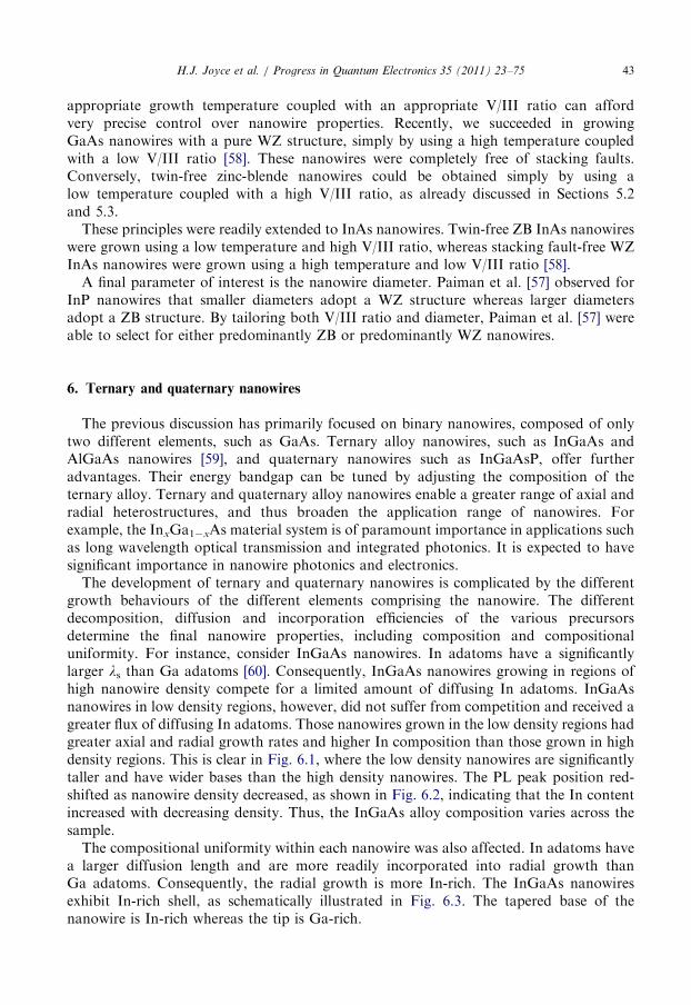
The development of ternary and quaternary nanowires is complicated by the differentgrowth behaviours of the different elements comprising the nanowire. The differentdecomposition, diffusion and incorporation efficiencies of the various precursorsdetermine the final nanowire properties, including composition and compositionaluniformity. For instance, consider InGaAs nanowires. In adatoms have a significantlylarger ls than Ga adatoms [60]. Consequently, InGaAs nanowires growing in regions ofhigh nanowire density compete for a limited amount of diffusing In adatoms. InGaAsnanowires in low density regions, however, did not suffer from competition and received agreater flux of diffusing In adatoms. Those nanowires grown in the low density regions hadgreater axial and radial growth rates and higher In composition than those grown in highdensity regions. This is clear in Fig. 6.1, where the low density nanowires are significantlytaller and have wider bases than the high density nanowires. The PL peak position red-shifted as nanowire density decreased, as shown in Fig. 6.2, indicating that the In contentincreased with decreasing density. Thus, the InGaAs alloy composition varies across thesample.
The compositional uniformity within each nanowire was also affected. In adatoms havea larger diffusion length and are more readily incorporated into radial growth thanGa adatoms. Consequently, the radial growth is more In-rich. The InGaAs nanowiresexhibit In-rich shell, as schematically illustrated in Fig. 6.3. The tapered base of thenanowire is In-rich whereas the tip is Ga-rich.
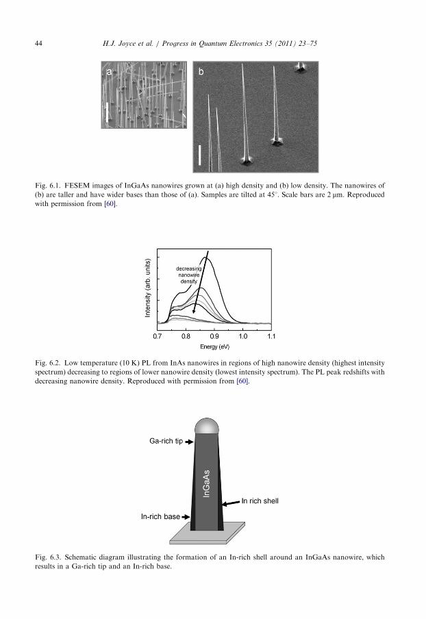
Fig. 6.1. FESEM images of InGaAs nanowires grown at (a) high density and (b) low density. The nanowires of
(b) are taller and have wider bases than those of (a). Samples are tilted at 451. Scale bars are 2 mm. Reproduced
with permission from [60].
Fig. 6.2. Low temperature (10 K) PL from InAs nanowires in regions of high nanowire density (highest intensity
spectrum) decreasing to regions of lower nanowire density (lowest intensity spectrum). The PL peak redshifts with
decreasing nanowire density. Reproduced with permission from [60].
Fig. 6.3. Schematic diagram illustrating the formation of an In-rich shell around an InGaAs nanowire, which
results in a Ga-rich tip and an In-rich base.
H.J. Joyce et al. / Progress in Quantum Electronics 35 (2011) 23–7544
H.J. Joyce et al. / Progress in Quantum Electronics 35 (2011) 23–75 45
7. Heterostructure nanowires
The cylindrical symmetry of nanowires permits two types of heterostructure: axial and radial.
7.1. Axial nanowire heterostructures
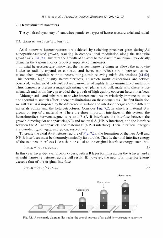
Axial nanowire heterostructures are achieved by switching precursor gases during Aunanoparticle-assisted growth, resulting in compositional modulation along the nanowiregrowth axis. Fig. 7.1 illustrates the growth of an axial heterostructure nanowire. Periodicallychanging the vapour species produces superlattice nanowires.
In axial heterostructure nanowires, the narrow nanowire diameter allows the nanowirelattice to radially expand or contract, and hence can relieve strain between lattice-mismatched materials without necessitating strain-relieving misfit dislocations [61,62].This permits high quality heterointerfaces, at which misfit dislocations are seldomobserved, within axial heterostructure nanowires of highly lattice-mismatched materials.Thus, nanowires present a major advantage over planar and bulk materials, where latticemismatch and strain have precluded the growth of high quality coherent heterointerfaces.
Although axial and substrate–nanowire heterostructures are relatively immune to latticeand thermal mismatch effects, there are limitations on these structures. The first limitationwe will discuss is imposed by the difference in surface and interface energies of the differentmaterials comprising the heterostructures. Consider Fig. 7.2, in which a material B isgrown on top of a material A. There are three important interfaces in this system: theheterointerface between segments A and B (A–B interface), the interface between thegrowth-directing Au nanoparticle (NP) and material A (NP–A interface), and the interfacebetween the Au nanoparticle and material B (NP–B interface). Their interfacial energiesare denoted gA–B, gNP–A and gNP–B, respectively.
To create the axial A–B heterostructure of Fig. 7.2a, the formation of the new A–B andNP–B interfaces must be thermodynamically favourable. That is, the total interface energyof the two new interfaces is less than or equal to the original interface energy, such that
gNP2B þ gA2BrgNP2A: ð1Þ
In this case, layer-by-layer growth occurs, with a B layer forming across the A layer, and astraight nanowire heterostructure will result. If, however, the new total interface energyexceeds that of the original interface,
gNP2B þ gA2B4gNP2A; ð2Þ
Fig. 7.1. A schematic diagram illustrating the growth process of an axial heterostructure nanowire.
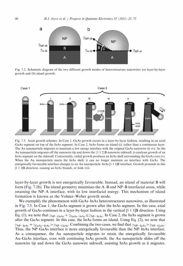
Fig. 7.2. Schematic diagram of the two different growth modes of heterostructure nanowires: (a) layer-by-layer
growth and (b) island growth.
Fig. 7.3. Axial growth schemes. In Case 1, GaAs growth occurs in a layer-by-layer fashion, resulting in an axial
GaAs segment on top of the InAs segment. In Case 2, InAs forms an island (i), rather than a continuous layer.
The Au nanoparticle migrates to maintain a low energy interface with the original GaAs nanowire (ii–iv). As the
Au nanoparticle migrates off the nanowire tip and down the {1 1 2}B nanowire sidewall, it catalyses growth of an
InAs segment on the sidewall. Concurrently, radial growth produces an InAs shell surrounding the GaAs core (v).
When the Au nanoparticle meets the InAs shell, it can no longer maintain an interface with GaAs. The
energetically favourable interface changes to an Au nanoparticle–InAs [1 1 1]B interface. Growth proceeds in this
[1 1 1]B direction, causing an InAs branch, or kink (vi).
H.J. Joyce et al. / Progress in Quantum Electronics 35 (2011) 23–7546
layer-by-layer growth is not energetically favourable. Instead, an island of material B willform (Fig. 7.2b). The island geometry minimises the A–B and NP–B interfacial areas, whileretaining the NP–A interface, with its low interfacial energy. This mechanism of islandformation is known as the Volmer–Weber growth mode.We exemplify the phenomenon with GaAs–InAs heterostructures nanowires, as illustrated
in Fig. 7.3. In Case 1, the GaAs segment is grown after the InAs segment. In this case, axialgrowth of GaAs continues in a layer-by-layer fashion in the vertical [1 1 1]B direction. UsingEq. (1), we note that gNP2GaAs þ gGaAs2InAsrgNP2InAs. In Case 2, the InAs segment is grownafter the GaAs segment. In this case, the InAs forms an island. Using Eq. (2), we note thatgNP2InAs þ gGaAs2InAs4gNP2GaAs. Combining the two cases, we find that gNP2InAs4gNP2GaAs.Thus, the NP–GaAs interface is more energetically favourable than the NP–InAs interface.As a consequence, the Au nanoparticle migrates to retain the energetically favourableAu–GaAs interface, even with continuing InAs growth: the Au nanoparticle slides off thenanowire tip and down the GaAs nanowire sidewall, assisting InAs growth as it migrates.
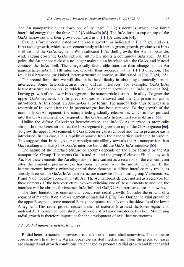
H.J. Joyce et al. / Progress in Quantum Electronics 35 (2011) 23–75 47
The Au nanoparticle slides down one of the three {1 1 2}B sidewalls, which have lowerinterfacial energy than the three {1 1 2}A sidewalls [63]. The InAs forms a cap on top of theGaAs nanowires and then grows downward in a [1 1 1]A direction [64].
Case 2 is further complicated by the radial growth, as indicated in Fig. 7.3(v) and (vi).InAs radial growth, which occurs concurrently with InAs segment growth, produces an InAsshell around the GaAs segment. With sufficient InAs shell growth, the Au nanoparticle,while sliding down the GaAs sidewall, ultimately meets a continuous InAs shell. At thispoint, the Au nanoparticle can no longer maintain an interface with the GaAs, and insteadcontacts the InAs shell. The energetically favourable interface then changes to an Aunanoparticle–InAs [1 1 1]B interface. Growth then proceeds in this [1 1 1]B direction. Theresult is a branched, or kinked, heterostructure nanowire, as illustrated in Fig. 7.3(vi) [65].
The second limitation we will discuss is the difficulty in obtaining atomically abruptinterfaces. Some heterostructures form diffuse interfaces, for example, GaAs/InAsheterostructure nanowires, in which a GaAs segment grows on an InAs segment [66].During growth of the lower InAs segment, the nanoparticle is an Au–In alloy. To grow theupper GaAs segment, the In precursor gas is removed and the Ga precursor gas isintroduced. At this point, an Au–In–Ga alloy forms. The nanoparticle thus behaves as areservoir of In, even after the In precursor gas has been removed. During growth of thenominally GaAs segment, the nanoparticle gradually releases In, which is incorporatedinto the GaAs segment. Consequently, the GaAs/InAs heterointerface is diffuse [66].
Unlike the diffuse GaAs/InAs heterointerface, the InAs/GaAs interface is atomicallyabrupt. In these heterostructures, the InAs segment is grown on top of the GaAs segment [66].To grow the upper InAs segment, the Ga precursor gas is removed and the In precursor gas isintroduced. In this case, Ga is rapidly expunged from the nanoparticle under the In vapour.This suggests that In has greater thermodynamic affinity towards the Au nanoparticle thanGa, resulting in a sharp InAs/GaAs interface but a diffuse GaAs/InAs interface [66].
The nature of the interface (diffuse or abrupt) depends on the alloy formed by the Aunanoparticle. Group III elements Ga, In and Al, and the group V element Sb, all alloy withAu. For these elements, the Au alloy nanoparticle can act as a reservoir of the element, evenafter the element’s precursor gas has been removed from the growth chamber. If theheterostructure involves switching one of these elements, a diffuse interface may result, asalready discussed for GaAs/InAs heterostructure nanowires. In contrast, group V elements As,P and N do not alloy appreciably with Au. The Au nanoparticle does not act as a reservoir forthese elements. If the heterostructure involves switching one of these elements to another, theinterface will be abrupt, for instance InAs/InP and GaP/GaAs heterostructures nanowires.
The third limitation is unintentional concurrent radial growth. Consider the growth of asegment of material B on a lower segment of material A (Fig. 7.4). During the axial growth ofthe upper B segment, some material B may incorporate radially onto the sidewalls of the lowerA segment. This radial growth creates a shell of material B around the lower segment ofmaterial A. This unintentional shell can adversely affect nanowire device function. Minimisingradial growth is therefore important for the development of axial heterostructures.
7.2. Radial nanowire heterostructures
Radial heterostructure nanowires are also known as core–shell nanowires. The nanowirecore is grown first, by the Au nanoparticle-assisted mechanism. Then the precursor gasesare changed and growth conditions are changed to promote radial growth and hinder axial
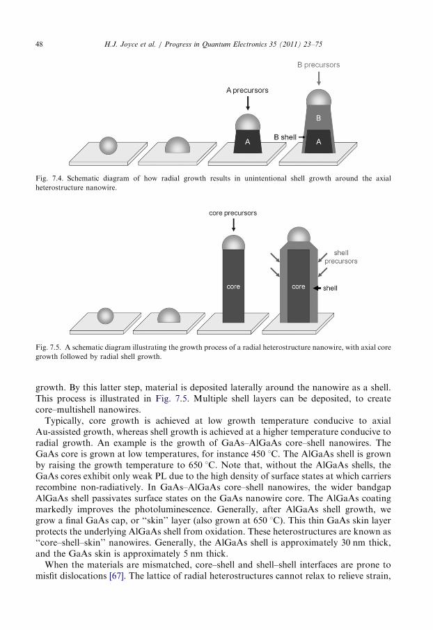
Fig. 7.4. Schematic diagram of how radial growth results in unintentional shell growth around the axial
heterostructure nanowire.
Fig. 7.5. A schematic diagram illustrating the growth process of a radial heterostructure nanowire, with axial core
growth followed by radial shell growth.
H.J. Joyce et al. / Progress in Quantum Electronics 35 (2011) 23–7548
growth. By this latter step, material is deposited laterally around the nanowire as a shell.This process is illustrated in Fig. 7.5. Multiple shell layers can be deposited, to createcore–multishell nanowires.Typically, core growth is achieved at low growth temperature conducive to axial
Au-assisted growth, whereas shell growth is achieved at a higher temperature conducive toradial growth. An example is the growth of GaAs–AlGaAs core–shell nanowires. TheGaAs core is grown at low temperatures, for instance 450 1C. The AlGaAs shell is grownby raising the growth temperature to 650 1C. Note that, without the AlGaAs shells, theGaAs cores exhibit only weak PL due to the high density of surface states at which carriersrecombine non-radiatively. In GaAs–AlGaAs core–shell nanowires, the wider bandgapAlGaAs shell passivates surface states on the GaAs nanowire core. The AlGaAs coatingmarkedly improves the photoluminescence. Generally, after AlGaAs shell growth, wegrow a final GaAs cap, or ‘‘skin’’ layer (also grown at 650 1C). This thin GaAs skin layerprotects the underlying AlGaAs shell from oxidation. These heterostructures are known as‘‘core–shell–skin’’ nanowires. Generally, the AlGaAs shell is approximately 30 nm thick,and the GaAs skin is approximately 5 nm thick.When the materials are mismatched, core–shell and shell–shell interfaces are prone to
misfit dislocations [67]. The lattice of radial heterostructures cannot relax to relieve strain,
H.J. Joyce et al. / Progress in Quantum Electronics 35 (2011) 23–75 49
unlike axial heterostructures. The crystal structure of the shell tends to follow thecrystallographic structure of the core: ZB shells grow on ZB cores (e.g. ZB InAs shells onZB GaAs cores) [67] and WZ shells grow on WZ cores (e.g. WZ GaAs shells on WZ InAscores) [68].
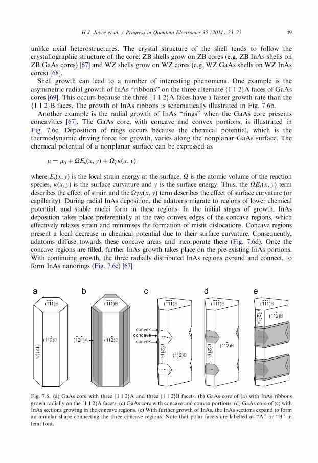
Shell growth can lead to a number of interesting phenomena. One example is theasymmetric radial growth of InAs ‘‘ribbons’’ on the three alternate {1 1 2}A faces of GaAscores [69]. This occurs because the three {1 1 2}A faces have a faster growth rate than the{1 1 2}B faces. The growth of InAs ribbons is schematically illustrated in Fig. 7.6b.
Another example is the radial growth of InAs ‘‘rings’’ when the GaAs core presentsconcavities [67]. The GaAs core, with concave and convex portions, is illustrated inFig. 7.6c. Deposition of rings occurs because the chemical potential, which is thethermodynamic driving force for growth, varies along the nonplanar GaAs surface. Thechemical potential of a nonplanar surface can be expressed as
m ¼ m0 þ OEs x; yð Þ þ Ogk x; yð Þ
where Es(x,y) is the local strain energy at the surface, O is the atomic volume of the reactionspecies, k(x,y) is the surface curvature and g is the surface energy. Thus, the OEsðx; yÞ termdescribes the effect of strain and the Ogkðx; yÞ term describes the effect of surface curvature (orcapillarity). During radial InAs deposition, the adatoms migrate to regions of lower chemicalpotential, and stable nuclei form in these regions. In the initial stages of growth, InAsdeposition takes place preferentially at the two convex edges of the concave regions, whicheffectively relaxes strain and minimises the formation of misfit dislocations. Concave regionspresent a local decrease in chemical potential due to their surface curvature. Consequently,adatoms diffuse towards these concave areas and incorporate there (Fig. 7.6d). Once theconcave regions are filled, further InAs growth takes place on the pre-existing InAs portions.With continuing growth, the three radially distributed InAs regions expand and connect, toform InAs nanorings (Fig. 7.6e) [67].
Fig. 7.6. (a) GaAs core with three {1 1 2}A and three {1 1 2}B facets. (b) GaAs core of (a) with InAs ribbons
grown radially on the {1 1 2}A facets. (c) GaAs core with concave and convex portions. (d) GaAs core of (c) with
InAs sections growing in the concave regions. (e) With further growth of InAs, the InAs sections expand to form
an annular shape connecting the three concave regions. Note that polar facets are labelled as ‘‘A’’ or ‘‘B’’ in
feint font.
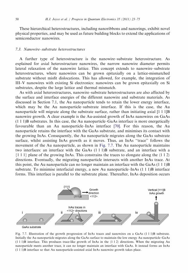
H.J. Joyce et al. / Progress in Quantum Electronics 35 (2011) 23–7550
These hierarchical heterostructures, including nanoribbons and nanorings, exhibit novelphysical properties, and may be used as future building blocks to extend the applications ofsemiconductor nanowires.
7.3. Nanowire–substrate heterostructures
A further type of heterostructure is the nanowire–substrate heterostructure. Asexplained for axial heterostructure nanowires, the narrow nanowire diameter permitslateral relaxation of the nanowire lattice. This concept extends to nanowire–substrateheterostructures, where nanowires can be grown epitaxially on a lattice-mismatchedsubstrate without misfit dislocations. This has allowed, for example, the integration ofIII–V nanowires with existing Si electronics: nanowires can be grown epitaxially on Sisubstrates, despite the large lattice and thermal mismatch.As with axial heterostructures, nanowire–substrate heterostructures are also affected by
the surface and interface energies of the different nanowire and substrate materials. Asdiscussed in Section 7.1, the Au nanoparticle tends to retain the lower energy interface,which may be the Au nanoparticle–substrate interface. If this is the case, the Aunanoparticle will migrate along the substrate surface, rather than initiating axial [1 1 1]Bnanowire growth. A clear example is the Au-assisted growth of InAs nanowires on GaAs(1 1 1)B substrates. In this case, the Au nanoparticle–GaAs interface is more energeticallyfavourable than an Au nanoparticle–InAs interface [70]. For this reason, the Aunanoparticle retains the interface with the GaAs substrate, and minimises its contact withthe growing InAs. Consequently, the Au nanoparticle migrates along the GaAs substratesurface, whilst assisting InAs growth as it moves. Thus, an InAs ‘‘trace’’ follows themovement of the Au nanoparticle, as shown in Fig. 7.7. The Au nanoparticle maintainstwo interfaces: an interface with the GaAs (1 1 1)B substrate, and an interface with a{1 1 1} plane of the growing InAs. This constrains the traces to elongate along the 1 1 2h i
directions. Eventually, the migrating nanoparticle intersects with another InAs trace. Atthis point, the Au nanoparticle can no longer maintain an interface with the GaAs (1 1 1)Bsubstrate. To minimise interfacial energy, a new Au nanoparticle–InAs (1 1 1)B interfaceforms. This interface is parallel to the substrate plane. Thereafter, InAs deposition occurs
Fig. 7.7. Illustration of the growth progression of InAs traces and nanowires on a GaAs (1 1 1)B substrate.
Initially the Au nanoparticle migrates along the GaAs surface to maintain the low energy Au nanoparticle–GaAs
(1 1 1)B interface. This produces trace-like growth of InAs in the 1 1 2h i directions. When the migrating Au
nanoparticle meets another trace, it can no longer maintain an interface with GaAs. It instead forms an InAs
(1 1 1)B interface so that Au nanoparticle-assisted axial InAs nanowire growth takes place.
H.J. Joyce et al. / Progress in Quantum Electronics 35 (2011) 23–75 51
at this Au nanoparticle–InAs (1 1 1)B interface so that vertical [1 1 1]B InAs nanowiregrowth takes place.
8. Photoluminescence spectroscopy of semiconductor nanowires
The optical and electronic properties of semiconductor nanowires and nanowireheterostructures can be probed using the powerful optical characterisation techniques ofphotoluminescence spectroscopy including continuous wave (CW-PL), resonant, time-resolved and polarisation spectroscopy. These techniques provide insights into thecrystalline quality, the energy bandgap (or bandgaps in the case of heterostructures), theexcitonic structure, crystalline defects, doping, crystalline phase, and spin and excitonlifetimes—all qualities relevant to particular nanowire device applications. In the sectionsbelow, we explore the contributions to our understanding of the III–V nanowires presentedin the previous sections. First we discuss CW-PL, then polarisation spectroscopy, resonantspectroscopy, time-resolved spectroscopy and finally Raman spectroscopy. We provideseveral key experimental details about each technique. In addition, we connect ourdiscussion of the results to the central qualities of nanowires identified via different growthparameters and materials to provide insights into a wide range of physical properties onecan determine from spectroscopic techniques, from bandgaps to exciton lifetimes. We payspecial attention to the properties of the nanowires that should enable flexible and uniquedevice applications.
Semiconductor nanowires are named appropriately in the sense that their diameters areclearly in the nanometre range, e.g. 20–100 nm, a scale that will be important, but a scaleoften not in the quantum regime. Since the exciton diameter is 24 nm for GaAs, 18 nm forInP, and 68 nm for InAs, quantum effects only begin to become important for nanowireswhose diameters are smaller than 20 nm. While the majority of the nanowires are grownwith 20, 30 and 50 nm gold catalysts, once the nanowires have grown 2–10 mm in the axial(lengthwise) direction, they almost always range from 30 to 80 nm in diameter. Thusquantum effects are nearly insignificant for the nanowires considered in this review. In fact,in the previous 10 years of growth, only a single paper on InP nanowires in 2001 [71] and asingle paper on GaAs in 2009 [72] showed conclusive evidence for quantum confinementeffects.
Nonetheless, dramatic effects on the electronic and optical properties of semiconductornanowires still occur on the o100 nm diameter length scale, in particular in two areas: forthe excitation and emission from these nanowires and in the diffusion of carriers within thenanowires. The relevant optical fields for excitation and emission from these nanowiresrange in wavelength from 700 to 1600 nm. The nanowire diameters studied here are smallerthan these wavelengths by an order of magnitude. As we shall show, this has dramaticconsequences on the excitation and emission of electronic states in nanowires. For carrieror exciton diffusion, the low temperature hole mobilities, ranging from 1000 for InP to10,000 cm2 V�1 s�1 for GaAs and recombination lifetimes (�1 ns) suggest diffusionlengths of several microns. This implies that the electrons and holes can sample nearly theentire volume of the nanowire during their lifetime. Thus the quality of surfaces orinterfaces of the nanowire and uniformity of dimensions are key elements in the nanowireproperties. Even for perfectly crystalline semiconductor nanowires (no defects), thevariability of the surface or interfaces of individual nanowires can result in quite dramaticchanges in their properties. Measurements of ensembles of nanowires, while informative,
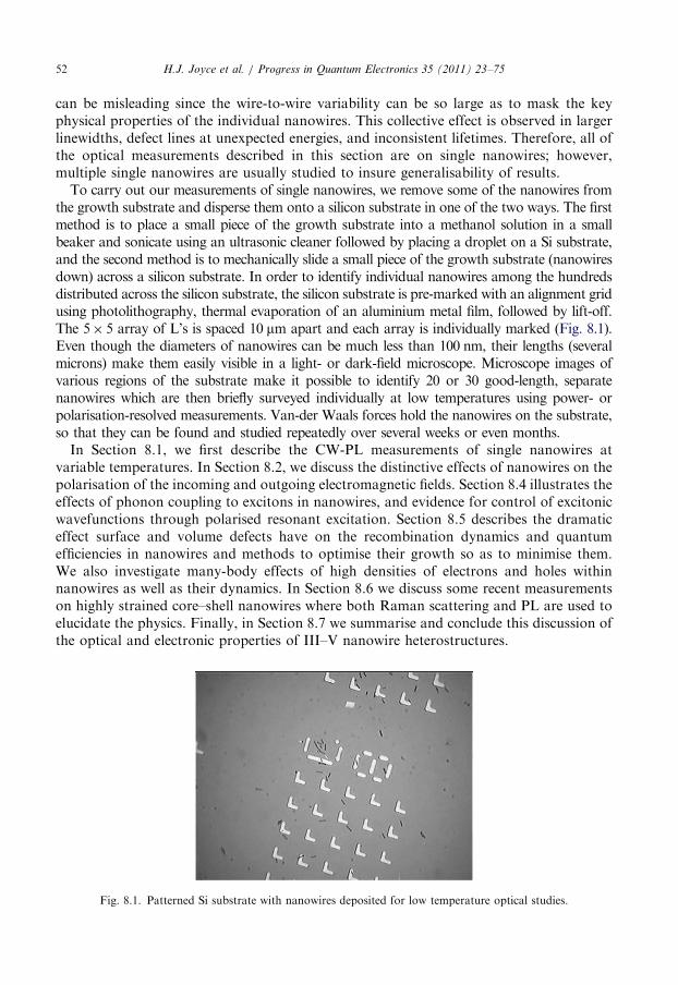
H.J. Joyce et al. / Progress in Quantum Electronics 35 (2011) 23–7552
can be misleading since the wire-to-wire variability can be so large as to mask the keyphysical properties of the individual nanowires. This collective effect is observed in largerlinewidths, defect lines at unexpected energies, and inconsistent lifetimes. Therefore, all ofthe optical measurements described in this section are on single nanowires; however,multiple single nanowires are usually studied to insure generalisability of results.To carry out our measurements of single nanowires, we remove some of the nanowires from
the growth substrate and disperse them onto a silicon substrate in one of the two ways. The firstmethod is to place a small piece of the growth substrate into a methanol solution in a smallbeaker and sonicate using an ultrasonic cleaner followed by placing a droplet on a Si substrate,and the second method is to mechanically slide a small piece of the growth substrate (nanowiresdown) across a silicon substrate. In order to identify individual nanowires among the hundredsdistributed across the silicon substrate, the silicon substrate is pre-marked with an alignment gridusing photolithography, thermal evaporation of an aluminium metal film, followed by lift-off.The 5� 5 array of L’s is spaced 10 mm apart and each array is individually marked (Fig. 8.1).Even though the diameters of nanowires can be much less than 100 nm, their lengths (severalmicrons) make them easily visible in a light- or dark-field microscope. Microscope images ofvarious regions of the substrate make it possible to identify 20 or 30 good-length, separatenanowires which are then briefly surveyed individually at low temperatures using power- orpolarisation-resolved measurements. Van-der Waals forces hold the nanowires on the substrate,so that they can be found and studied repeatedly over several weeks or even months.In Section 8.1, we first describe the CW-PL measurements of single nanowires at
variable temperatures. In Section 8.2, we discuss the distinctive effects of nanowires on thepolarisation of the incoming and outgoing electromagnetic fields. Section 8.4 illustrates theeffects of phonon coupling to excitons in nanowires, and evidence for control of excitonicwavefunctions through polarised resonant excitation. Section 8.5 describes the dramaticeffect surface and volume defects have on the recombination dynamics and quantumefficiencies in nanowires and methods to optimise their growth so as to minimise them.We also investigate many-body effects of high densities of electrons and holes withinnanowires as well as their dynamics. In Section 8.6 we discuss some recent measurementson highly strained core–shell nanowires where both Raman scattering and PL are used toelucidate the physics. Finally, in Section 8.7 we summarise and conclude this discussion ofthe optical and electronic properties of III–V nanowire heterostructures.
Fig. 8.1. Patterned Si substrate with nanowires deposited for low temperature optical studies.
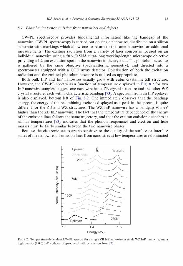
H.J. Joyce et al. / Progress in Quantum Electronics 35 (2011) 23–75 53
8.1. Photoluminescence emission from nanowires and defects
CW-PL spectroscopy provides fundamental information like the bandgap of thenanowire. CW-PL spectroscopy is carried out on single nanowires distributed on a siliconsubstrate with markings which allow one to return to the same nanowire for additionalmeasurements. The exciting radiation from a variety of laser sources is focused on anindividual nanowire using a 50� /0.5NA ultra-long working-length microscope objectiveproviding a 1.2 mm excitation spot on the nanowire in the cryostat. The photoluminescenceis gathered by the same objective (backscattering geometry), and directed into aspectrometer equipped with a CCD array detector. Polarisation of both the excitationradiation and the emitted photoluminescence is utilised as appropriate.
Both bulk InP and InP nanowires usually grow with cubic crystalline ZB structure.However, the CW-PL spectra as a function of temperature displayed in Fig. 8.2 for twoInP nanowire samples, suggest one nanowire has a ZB crystal structure and the other WZcrystal structure, each with a characteristic bandgap [73]. A spectrum from an InP epilayeris also displayed, bottom left of Fig. 8.2. One immediately observes that the bandgapenergy, the energy of the recombining excitons displayed as a peak in the spectra, is quitedifferent for the ZB and WZ structures. The WZ InP nanowire has a bandgap 80 meVhigher than the ZB InP nanowire. The fact that the temperature dependence of the energyof the emission lines follows the same trajectory, and that the exciton emission quenches atsimilar temperatures [73], indicates that the phonon frequencies and electron and holemasses must be fairly similar between the two nanowire phases.
Because the electronic states are so sensitive to the quality of the surface or interfacestates of the nanowire, all emission lines from nanowires at low temperatures are dominated
1.3
280K
Nor
m. I
nten
sity
(arb
. uni
ts)
Energy (eV)
Epilayer
Epilayer
20K
70K
160K
ZincblendeWurtzite
1.4 1.5
Fig. 8.2. Temperature-dependent CW-PL spectra for a single ZB InP nanowire, a single WZ InP nanowire, and a
high quality (1 0 0) InP epilayer. Reproduced with permission from [73].
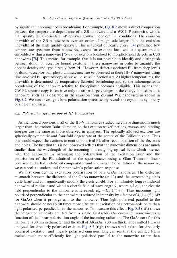
H.J. Joyce et al. / Progress in Quantum Electronics 35 (2011) 23–7554
by significant inhomogeneous broadening. For example, Fig. 8.2 shows a direct comparisonbetween the temperature dependence of a ZB nanowire and a WZ InP nanowire, with ahigh quality [1 0 0]-oriented InP epilayer grown under optimal conditions. The emissionlinewidth of the ZB nanowire is over an order of magnitude larger than the emissionlinewidth of the high quality epilayer. This is typical of nearly every [74] published lowtemperature spectrum from nanowires, except for excitons localised to a quantum dotembedded within a nanowire [75–77] or excitons localised to morphological defects in CdSnanowires [78]. This means, for example, that it is not possible to identify and distinguishbetween donor or acceptor bound excitons in these nanowires in order to quantify thedopant density and type directly from PL. However, defect-associated PL from deep levelsor donor–acceptor-pair photoluminescence can be observed in these III–V nanowires usingtime-resolved PL spectroscopy as we will discuss in Section 8.5. At higher temperatures, thelinewidth is determined by temperature (kinetic) broadening and so the inhomogeneousbroadening of the nanowire relative to the epilayer becomes negligible. This means thatCW-PL spectroscopy is sensitive only to rather large changes in the energy landscape of ananowire, such as is observed in the emission from ZB and WZ nanowires as shown inFig. 8.2. We now investigate how polarisation spectroscopy reveals the crystalline symmetryof single nanowires.
8.2. Polarisation spectroscopy of III–V nanowires
As mentioned previously, all of the III–V nanowires studied here have dimensions muchlarger than the exciton Bohr diameter, so that exciton wavefunctions, masses and bindingenergies are the same as those observed in epilayers. The optically allowed excitons arespherically symmetric and four-fold degenerate at the centre of the Brillouin zone. Thusone would expect the excitons to emit unpolarised PL after recombination of the electronsand holes. The fact that this is not observed reflects that the nanowire dimensions are muchsmaller than the wavelength of the incoming and outgoing optical fields which interactwith the nanowire. By arranging the polarisation of the excitation laser and thepolarisation of the PL admitted to the spectrometer using a Glan–Thomson linearpolariser and a Babinet–Soleil compensator and knowing the orientation of the nanowire,we can seek to understand the nanowire’s polarisation response.We first consider the excitation polarisation of bare GaAs nanowires. The dielectric
mismatch between the dielectric of the GaAs nanowire (e�13) and the surrounding air isquite large and can significantly modify the electric field. For an infinitely long cylindricalnanowire of radius r and with an electric field of wavelength l, where r/l51, the electricfield perpendicular to the nanowire is screened: Eint=Eext2/(1þe). Thus incoming lightpolarised perpendicular to the nanowire is reduced in intensity by a factor of 4/(1þe)2 (1/49for GaAs) when it propagates into the nanowire. Thus light polarised parallel to thenanowire should be nearly 50 times more efficient at excitation of electron–hole pairs thanlight polarised perpendicular to the nanowire. To measure this effect, Fig. 8.3 (left) showsthe integrated intensity emitted from a single GaAs/AlGaAs core–shell nanowire as afunction of the linear polarisation angle of the incoming radiation. The GaAs core for thisnanowire is 30 nm in diameter and the shell of AlGaAs is 30 nm thick. The emitted PL wasanalysed for circularly polarised exciton. Fig. 8.3 (right) shows similar data for circularlypolarised excitation and linearly polarised emission. One can see that the emitted PL isexcited much more efficiently for light polarised parallel to the nanowire rather than
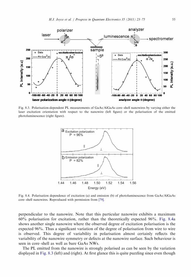
⊥
||
P = 96%Excitation polarization
||⊥
1.44
P = 82%Emission polarization
Energy (eV)1.46 1.48 1.50 1.52 1.54 1.56
Fig. 8.4. Polarisation dependence of excitation (a) and emission (b) of photoluminescence from GaAs/AlGaAs
core–shell nanowires. Reproduced with permission from [79].
Fig. 8.3. Polarisation-dependent PL measurements of GaAs/AlGaAs core–shell nanowires by varying either the
laser excitation orientation with respect to the nanowire (left figure) or the polarisation of the emitted
photoluminescence (right figure).
H.J. Joyce et al. / Progress in Quantum Electronics 35 (2011) 23–75 55
perpendicular to the nanowire. Note that this particular nanowire exhibits a maximum60% polarisation for excitation, rather than the theoretically expected 96%. Fig. 8.4ashows another single nanowire where the observed degree of excitation polarisation is theexpected 96%. Thus a significant variation of the degree of polarisation from wire to wireis observed. This degree of variability in polarisation almost certainly reflects thevariability of the nanowire symmetry or defects at the nanowire surface. Such behaviour isseen in core–shell as well as bare GaAs NWs.
The PL emitted from the nanowire is strongly polarised as can be seen by the variationdisplayed in Fig. 8.3 (left) and (right). At first glance this is quite puzzling since even though
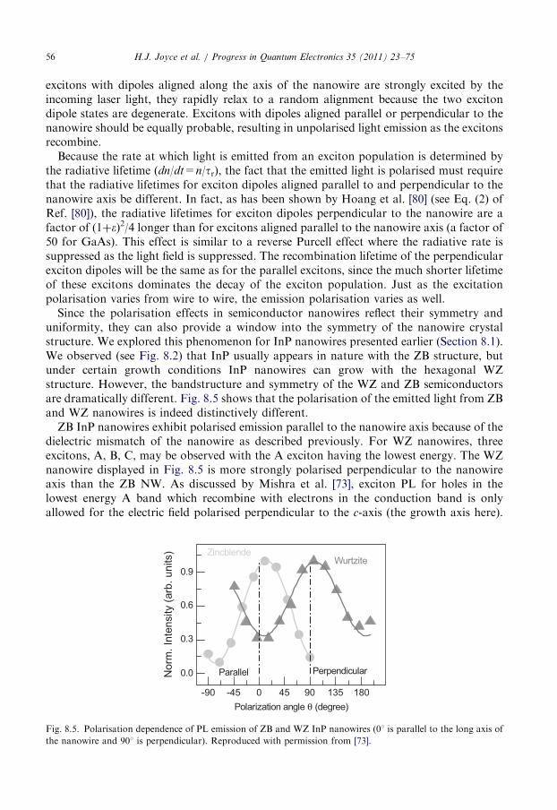
H.J. Joyce et al. / Progress in Quantum Electronics 35 (2011) 23–7556
excitons with dipoles aligned along the axis of the nanowire are strongly excited by theincoming laser light, they rapidly relax to a random alignment because the two excitondipole states are degenerate. Excitons with dipoles aligned parallel or perpendicular to thenanowire should be equally probable, resulting in unpolarised light emission as the excitonsrecombine.Because the rate at which light is emitted from an exciton population is determined by
the radiative lifetime (dn/dt=n/tr), the fact that the emitted light is polarised must requirethat the radiative lifetimes for exciton dipoles aligned parallel to and perpendicular to thenanowire axis be different. In fact, as has been shown by Hoang et al. [80] (see Eq. (2) ofRef. [80]), the radiative lifetimes for exciton dipoles perpendicular to the nanowire are afactor of (1þe)2/4 longer than for excitons aligned parallel to the nanowire axis (a factor of50 for GaAs). This effect is similar to a reverse Purcell effect where the radiative rate issuppressed as the light field is suppressed. The recombination lifetime of the perpendicularexciton dipoles will be the same as for the parallel excitons, since the much shorter lifetimeof these excitons dominates the decay of the exciton population. Just as the excitationpolarisation varies from wire to wire, the emission polarisation varies as well.Since the polarisation effects in semiconductor nanowires reflect their symmetry and
uniformity, they can also provide a window into the symmetry of the nanowire crystalstructure. We explored this phenomenon for InP nanowires presented earlier (Section 8.1).We observed (see Fig. 8.2) that InP usually appears in nature with the ZB structure, butunder certain growth conditions InP nanowires can grow with the hexagonal WZstructure. However, the bandstructure and symmetry of the WZ and ZB semiconductorsare dramatically different. Fig. 8.5 shows that the polarisation of the emitted light from ZBand WZ nanowires is indeed distinctively different.ZB InP nanowires exhibit polarised emission parallel to the nanowire axis because of the
dielectric mismatch of the nanowire as described previously. For WZ nanowires, threeexcitons, A, B, C, may be observed with the A exciton having the lowest energy. The WZnanowire displayed in Fig. 8.5 is more strongly polarised perpendicular to the nanowireaxis than the ZB NW. As discussed by Mishra et al. [73], exciton PL for holes in thelowest energy A band which recombine with electrons in the conduction band is onlyallowed for the electric field polarised perpendicular to the c-axis (the growth axis here).
-90
0.0
0.3
0.6
0.9
Nor
m. I
nten
sity
(arb
. uni
ts)
PerpendicularParallel
Polarization angle θ (degree)
ZincblendeWurtzite
-45 0 45 90 135 180
Fig. 8.5. Polarisation dependence of PL emission of ZB and WZ InP nanowires (01 is parallel to the long axis of
the nanowire and 901 is perpendicular). Reproduced with permission from [73].
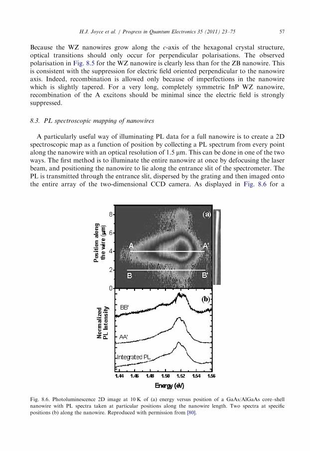
H.J. Joyce et al. / Progress in Quantum Electronics 35 (2011) 23–75 57
Because the WZ nanowires grow along the c-axis of the hexagonal crystal structure,optical transitions should only occur for perpendicular polarisations. The observedpolarisation in Fig. 8.5 for the WZ nanowire is clearly less than for the ZB nanowire. Thisis consistent with the suppression for electric field oriented perpendicular to the nanowireaxis. Indeed, recombination is allowed only because of imperfections in the nanowirewhich is slightly tapered. For a very long, completely symmetric InP WZ nanowire,recombination of the A excitons should be minimal since the electric field is stronglysuppressed.
8.3. PL spectroscopic mapping of nanowires
A particularly useful way of illuminating PL data for a full nanowire is to create a 2Dspectroscopic map as a function of position by collecting a PL spectrum from every pointalong the nanowire with an optical resolution of 1.5 mm. This can be done in one of the twoways. The first method is to illuminate the entire nanowire at once by defocusing the laserbeam, and positioning the nanowire to lie along the entrance slit of the spectrometer. ThePL is transmitted through the entrance slit, dispersed by the grating and then imaged ontothe entire array of the two-dimensional CCD camera. As displayed in Fig. 8.6 for a
Fig. 8.6. Photoluminescence 2D image at 10 K of (a) energy versus position of a GaAs/AlGaAs core–shell
nanowire with PL spectra taken at particular positions along the nanowire length. Two spectra at specific
positions (b) along the nanowire. Reproduced with permission from [80].
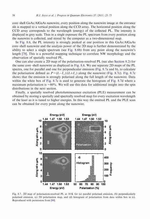
H.J. Joyce et al. / Progress in Quantum Electronics 35 (2011) 23–7558
core–shell GaAs/AlGaAs nanowire, every position along the nanowire image at the entranceslit is mapped to a vertical position along the CCD array. The horizontal position along theCCD array corresponds to the wavelength (energy) of the collected PL. The intensity isdisplayed in grey scale. Thus in a single exposure the PL spectrum from every position alongthe nanowire is collected, and stored by the computer as a two-dimensional map.In Fig. 8.6, the PL intensity is strongly peaked at one position in this GaAs/AlGaAs
core–shell nanowire and the analysis power of the 2D map is further demonstrated by theability to select a single spectrum (see Fig. 8.6b) from any point along the nanowire’slength [78]. This is a powerful mapping technique to correlate NW morphology and theobservation of spatially resolved PL.One can also create a 2D map of the polarisation-resolved PL (see also Section 8.2) for
the same core–shell nanowire as displayed in Fig. 8.6. We use separate 2D maps of the PLspectra, one for parallel and one for perpendicular emission (Fig. 8.7a and b), to calculatethe polarisation defined as P=(IJ�I?)/(IJþI?) along the nanowire (Fig. 8.7c). Fig. 8.7cshows that the emission is strongly polarised along the full length of the nanowire. Datawithin the white box of Fig. 8.7c is used to generate the histogram of Fig. 8.7d where amaximum polarisation is �80%. We will use this data for additional insight into the spindistributions in the next section.Finally, a spatially resolved photoluminescence excitation (PLE) measurement can be
obtained by storing a spatially and spectrally resolved map for every excitation wavelengthof the laser as it is tuned to higher energies. In this way the emitted PL and the PLE scancan be obtained for every point along the nanowire.
Fig. 8.7. 2D map of polarisation-resolved PL at 10 K for (a) parallel polarised emission, (b) perpendicularly
polarised emission, (c) 2D polarisation map, and (d) histogram of polarisation from data within box in (c).
Reproduced with permission from [80].
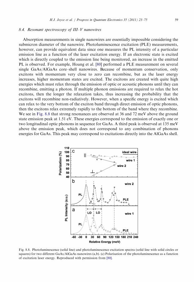
H.J. Joyce et al. / Progress in Quantum Electronics 35 (2011) 23–75 59
8.4. Resonant spectroscopy of III–V nanowires
Absorption measurements in single nanowires are essentially impossible considering thesubmicron diameter of the nanowire. Photoluminescence excitation (PLE) measurements,however, can provide equivalent data since one measures the PL intensity of a particularemission line as a function of the laser excitation energy. If an electronic state is excitedwhich is directly coupled to the emission line being monitored, an increase in the emittedPL is observed. For example, Hoang et al. [80] performed a PLE measurement on severalsingle GaAs/AlGaAs core–shell nanowires. Because of momentum conservation, onlyexcitons with momentum very close to zero can recombine, but as the laser energyincreases, higher momentum states are excited. The excitons are created with quite highenergies which must relax through the emission of optic or acoustic phonons until they canrecombine, emitting a photon. If multiple phonon emissions are required to relax the hotexcitons, then the longer the relaxation takes, thus increasing the probability that theexcitons will recombine non-radiatively. However, when a specific energy is excited whichcan relax to the very bottom of the exciton band through direct emission of optic phonons,then the excitons relax extremely rapidly to the bottom of the band where they recombine.We see in Fig. 8.8 that strong resonances are observed at 36 and 72 meV above the groundstate emission peak at 1.51 eV. These energies correspond to the emission of exactly one ortwo longitudinal optic phonons in sequence for GaAs. A third peak is observed at 135 meVabove the emission peak, which does not correspond to any combination of phononsenergies for GaAs. This peak may correspond to excitations directly into the AlGaAs shell.
Fig. 8.8. Photoluminescence (solid line) and photoluminescence excitation spectra (solid line with solid circles or
squares) for two different GaAs/AlGaAs nanowires (a,b). (c) Polarisation of the photoluminescence as a function
of excitation laser energy. Reproduced with permission from [80].
H.J. Joyce et al. / Progress in Quantum Electronics 35 (2011) 23–7560
The 135 meV energy corresponds to an aluminium concentration of �13%, only half the26% AlGaAs concentration expected from growth, suggesting that growth of the shell maybe limited by diffusion of the constituent atoms along the substrate surface, as was seenpreviously in InGaAs nanowires by Kim et al. [60].Resonant spectroscopy also provides insight into the behaviour of spins in these systems.
As one excites higher and higher into the exciton band, the excitons must relax throughmore and more scatterings in order to relax to the bottom of the band. If the excitationlaser is polarised parallel or perpendicular to the nanowire, the exciton is created with itsdipole oriented either parallel or perpendicular to the nanowire as well. In Fig. 8.8, wemonitor the polarisation of the emitted light as a function of the excitation energy. Notsurprisingly, at high energies for wire 2, the emitted polarisation is the same regardless ofthe orientation of the laser. This makes sense because the exciton dipoles will randomisethrough these scattering processes. What is very interesting is that as the laser energy isreduced, this symmetry is now broken. For parallel excitation, the emission PL is morestrongly polarised parallel to the nanowire. For perpendicular excitation the emission PLbecomes less strongly polarised. This is consistent with the formation of nonthermaldistributions of excitons with more parallel dipoles for parallel laser excitation, and moreperpendicular dipoles for perpendicular excitation. Converting parallel dipoles to perpen-dicular and vice versa requires a spin-flip process, so measuring the relaxation of parallel toperpendicular excitons with laser excitation energy directly measures the spin relaxationtime in these nanowires. Through rate-equation analysis solved in steady state (these areCW measurements), we find that the spin relaxation time increases by an order of magni-tude as the laser energy comes closer and closer to resonance with the emission line. Weestimate that the spin relaxation time is at most 50 ps for resonant excitation [80].
8.5. Time-resolved photoluminescence spectroscopy
Time-resolved photoluminescence (TRPL) spectroscopy provides insights into thedynamics of the excitons in nanowires. These measurements are important both forexploring basic science, and for assessing the suitability of nanowires for active devicestructures. After brief comments on the experimental aspects of TRPL, we provide threeexamples that illustrate the power of the technique, one of GaAs nanowires, one of InPnanowires, and finally one involving defects in GaAs nanowires.Time-resolved PL measurements are obtained by focusing the pulsed laser to a particular
point on the nanowire, collecting and dispersing the emitted PL in a spectrometer anddetecting the emitted photons by either a fast micro-channel plate phototube (MCPT) or asilicon APD with a 100 mm2 active area. Time-correlated photon counting is used [81,82] toaccumulate a statistical histogram of the number of photons collected as a function of arrivaltime after excitation by the laser pulse in order to show the decay of the PL. The systemresponse in our case is less than 80 ps. Full time-resolved spectra are collected by accumulatingtime-decays as a function of the wavelength of the spectrometer. This allows one to construct a2D plot of intensity vs. energy and time.Very recently we have obtained TRPL results from the twin-free GaAs/AlGaAs core–
shell nanowire heterostructures. The twin-free GaAs cores were grown by the two-temperature procedure discussed in Section 5.2. These core–shell nanowires were cappedby an �5 nm layer of GaAs to prevent oxidation of the AlGaAs which is a potential sourceof oxygen defects in the core. Earlier TRPL results of GaAs/AlGaAs core–shell nanowires
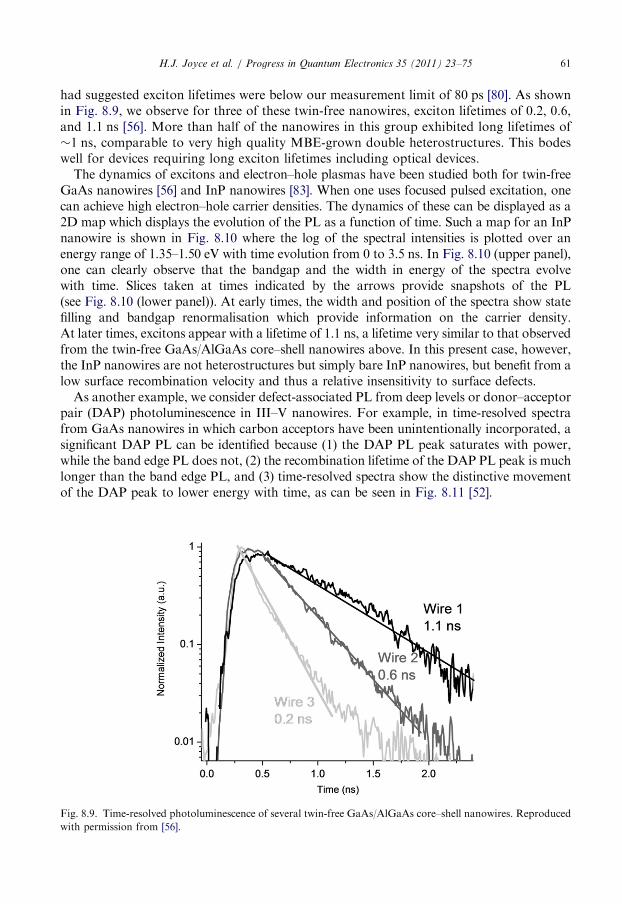
H.J. Joyce et al. / Progress in Quantum Electronics 35 (2011) 23–75 61
had suggested exciton lifetimes were below our measurement limit of 80 ps [80]. As shownin Fig. 8.9, we observe for three of these twin-free nanowires, exciton lifetimes of 0.2, 0.6,and 1.1 ns [56]. More than half of the nanowires in this group exhibited long lifetimes of�1 ns, comparable to very high quality MBE-grown double heterostructures. This bodeswell for devices requiring long exciton lifetimes including optical devices.
The dynamics of excitons and electron–hole plasmas have been studied both for twin-freeGaAs nanowires [56] and InP nanowires [83]. When one uses focused pulsed excitation, onecan achieve high electron–hole carrier densities. The dynamics of these can be displayed as a2D map which displays the evolution of the PL as a function of time. Such a map for an InPnanowire is shown in Fig. 8.10 where the log of the spectral intensities is plotted over anenergy range of 1.35–1.50 eV with time evolution from 0 to 3.5 ns. In Fig. 8.10 (upper panel),one can clearly observe that the bandgap and the width in energy of the spectra evolvewith time. Slices taken at times indicated by the arrows provide snapshots of the PL(see Fig. 8.10 (lower panel)). At early times, the width and position of the spectra show statefilling and bandgap renormalisation which provide information on the carrier density.At later times, excitons appear with a lifetime of 1.1 ns, a lifetime very similar to that observedfrom the twin-free GaAs/AlGaAs core–shell nanowires above. In this present case, however,the InP nanowires are not heterostructures but simply bare InP nanowires, but benefit from alow surface recombination velocity and thus a relative insensitivity to surface defects.
As another example, we consider defect-associated PL from deep levels or donor–acceptorpair (DAP) photoluminescence in III–V nanowires. For example, in time-resolved spectrafrom GaAs nanowires in which carbon acceptors have been unintentionally incorporated, asignificant DAP PL can be identified because (1) the DAP PL peak saturates with power,while the band edge PL does not, (2) the recombination lifetime of the DAP PL peak is muchlonger than the band edge PL, and (3) time-resolved spectra show the distinctive movementof the DAP peak to lower energy with time, as can be seen in Fig. 8.11 [52].
Fig. 8.9. Time-resolved photoluminescence of several twin-free GaAs/AlGaAs core–shell nanowires. Reproduced
with permission from [56].
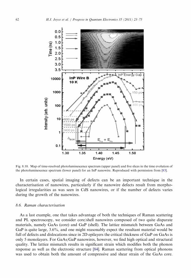
Fig. 8.10. Map of time-resolved photoluminescence spectrum (upper panel) and five slices in the time evolution of
the photoluminescence spectrum (lower panel) for an InP nanowire. Reproduced with permission from [83].
H.J. Joyce et al. / Progress in Quantum Electronics 35 (2011) 23–7562
In certain cases, spatial imaging of defects can be an important technique in thecharacterisation of nanowires, particularly if the nanowire defects result from morpho-logical irregularities as was seen in CdS nanowires, or if the number of defects variesduring the growth of the nanowires.
8.6. Raman characterisation
As a last example, one that takes advantage of both the techniques of Raman scatteringand PL spectroscopy, we consider core/shell nanowires composed of two quite disparatematerials, namely GaAs (core) and GaP (shell). The lattice mismatch between GaAs andGaP is quite large, 3.6%, and one might reasonably expect the resultant material would befull of defects and dislocations since in 2D epilayers the critical thickness of GaP on GaAs isonly 5 monolayers. For GaAs/GaP nanowires, however, we find high optical and structuralquality. The lattice mismatch results in significant strain which modifies both the phononresponse as well as the electronic structure [84]. Raman scattering from optical phononswas used to obtain both the amount of compressive and shear strain of the GaAs core.
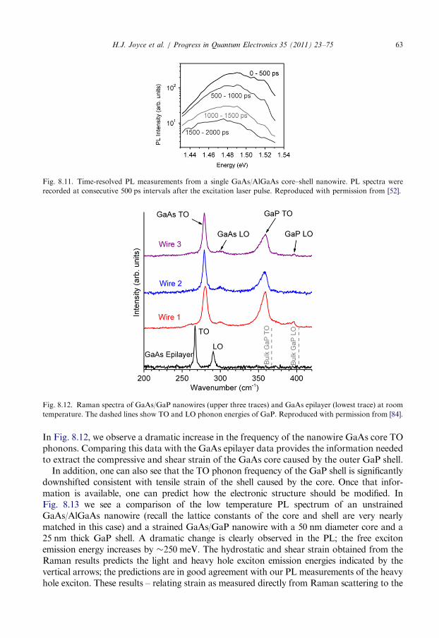
Fig. 8.12. Raman spectra of GaAs/GaP nanowires (upper three traces) and GaAs epilayer (lowest trace) at room
temperature. The dashed lines show TO and LO phonon energies of GaP. Reproduced with permission from [84].
Fig. 8.11. Time-resolved PL measurements from a single GaAs/AlGaAs core–shell nanowire. PL spectra were
recorded at consecutive 500 ps intervals after the excitation laser pulse. Reproduced with permission from [52].
H.J. Joyce et al. / Progress in Quantum Electronics 35 (2011) 23–75 63
In Fig. 8.12, we observe a dramatic increase in the frequency of the nanowire GaAs core TOphonons. Comparing this data with the GaAs epilayer data provides the information neededto extract the compressive and shear strain of the GaAs core caused by the outer GaP shell.
In addition, one can also see that the TO phonon frequency of the GaP shell is significantlydownshifted consistent with tensile strain of the shell caused by the core. Once that infor-mation is available, one can predict how the electronic structure should be modified. InFig. 8.13 we see a comparison of the low temperature PL spectrum of an unstrainedGaAs/AlGaAs nanowire (recall the lattice constants of the core and shell are very nearlymatched in this case) and a strained GaAs/GaP nanowire with a 50 nm diameter core and a25 nm thick GaP shell. A dramatic change is clearly observed in the PL; the free excitonemission energy increases by �250 meV. The hydrostatic and shear strain obtained from theRaman results predicts the light and heavy hole exciton emission energies indicated by thevertical arrows; the predictions are in good agreement with our PL measurements of the heavyhole exciton. These results – relating strain as measured directly from Raman scattering to the
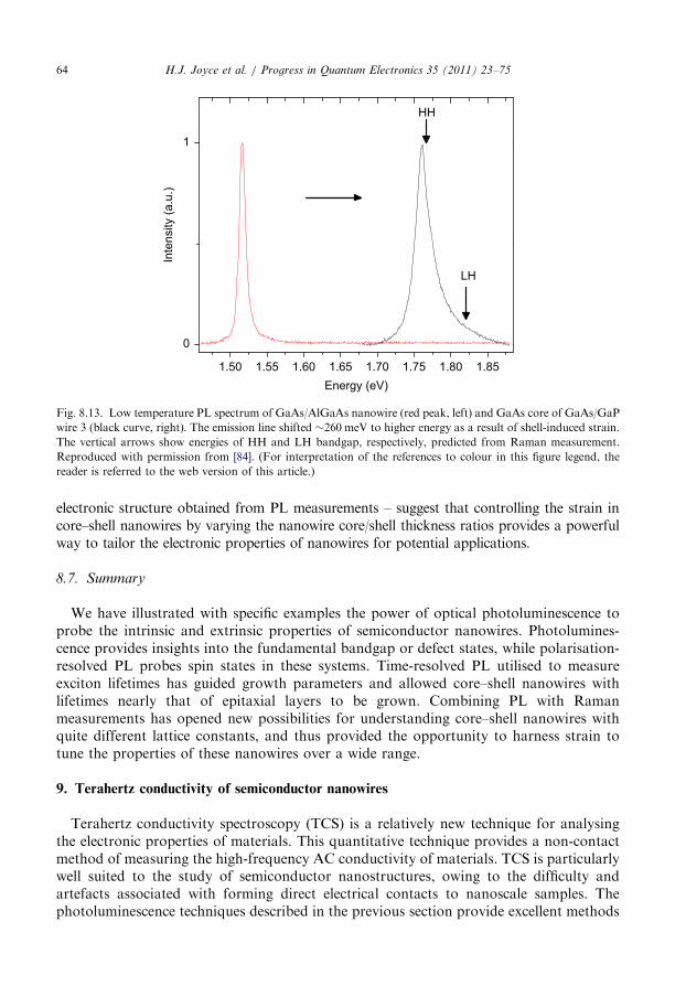
1.50
0
1
LH
Inte
nsity
(a.u
.)
Energy (eV)
HH
1.55 1.60 1.65 1.70 1.75 1.80 1.85
Fig. 8.13. Low temperature PL spectrum of GaAs/AlGaAs nanowire (red peak, left) and GaAs core of GaAs/GaP
wire 3 (black curve, right). The emission line shifted �260 meV to higher energy as a result of shell-induced strain.
The vertical arrows show energies of HH and LH bandgap, respectively, predicted from Raman measurement.
Reproduced with permission from [84]. (For interpretation of the references to colour in this figure legend, the
reader is referred to the web version of this article.)
H.J. Joyce et al. / Progress in Quantum Electronics 35 (2011) 23–7564
electronic structure obtained from PL measurements – suggest that controlling the strain incore–shell nanowires by varying the nanowire core/shell thickness ratios provides a powerfulway to tailor the electronic properties of nanowires for potential applications.
8.7. Summary
We have illustrated with specific examples the power of optical photoluminescence toprobe the intrinsic and extrinsic properties of semiconductor nanowires. Photolumines-cence provides insights into the fundamental bandgap or defect states, while polarisation-resolved PL probes spin states in these systems. Time-resolved PL utilised to measureexciton lifetimes has guided growth parameters and allowed core–shell nanowires withlifetimes nearly that of epitaxial layers to be grown. Combining PL with Ramanmeasurements has opened new possibilities for understanding core–shell nanowires withquite different lattice constants, and thus provided the opportunity to harness strain totune the properties of these nanowires over a wide range.
9. Terahertz conductivity of semiconductor nanowires
Terahertz conductivity spectroscopy (TCS) is a relatively new technique for analysingthe electronic properties of materials. This quantitative technique provides a non-contactmethod of measuring the high-frequency AC conductivity of materials. TCS is particularlywell suited to the study of semiconductor nanostructures, owing to the difficulty andartefacts associated with forming direct electrical contacts to nanoscale samples. Thephotoluminescence techniques described in the previous section provide excellent methods
H.J. Joyce et al. / Progress in Quantum Electronics 35 (2011) 23–75 65
of characterising semiconductor nanowires. However in order to study the electronicproperties of materials with these techniques charge carriers in the samples must bephotoexcited and relax via a path involving a reasonably strong radiative transition. Forexample, the photoluminescence of bare GaAs nanowires is heavily quenched by non-radiative transitions, hence these samples cannot be analysed easily by photoluminescencespectroscopy [79]. TCS measures the dielectric response of a material, and hence does notrequire the material to emit light, or even be photoexcited.
The simplest form of TCS measures the dielectric response of a material by probing itwith a single-cycle electromagnetic pulse of approximately 1 ps duration (this transient isoften called a ‘‘terahertz’’ pulse, owing to its peak frequency components being in the THzregion when Fourier transformed). In this form of TCS, the sample does not need to bephotoexcited. A typical spectrometer can measure the complex conductivity of a materialover a frequency range from �0.1 to �3 THz. The spectrometer does not just providecalibrated values of the conductivity; the frequency dependence of the conductivityspectrum also provides a wealth of information about the mechanisms of charge transportin the material.
TCS may also be used to study how the dielectric properties of a material change as afunction of time after photoexcitation. In this form of the technique a laser pulse is used tophotoexcite the sample and a picosecond electromagnetic ‘‘terahertz’’ pulse is used toanalyse the conductivity spectrum at set times after the photoexcitation event. In this wayit is possible to observe (i) the portion of the sample’s conductivity that occurs just as aresult of photogenerated charge carriers and (ii) how the charge dynamics change on atimescale from �100 fs to 41 ns after photoexcitation.
It is informative to consider why it is useful to analyse complex conductivity ofnanowires at terahertz frequencies (n�0.1–3 THz). The best way to put this into contextis to consider the energy carried by photon of this frequency range (hn�0.4–13 meV).For inorganic semiconductors this is an energy range of collective excitations suchas plasmons, excitons and phonons. Thus the occurrence and properties of any ofthese collective excitations in a sample may be clearly identified by the presence oftheir signature in the terahertz conductivity spectrum [85,86]. For example, if asemiconductor exhibits a classic Drude-type conductivity of a ‘‘free’’ electron gas thenTCS measurements would reveal a spectrum similar to that shown in Fig. 9.1a. In contrast,if the charge carriers were bound as excitons, a Lorentzian conductivity spectrum wouldresult, as shown in Fig. 9.1b. It is also important to note that the 0.4–13 meV-rangecovered by TCS is non-resonant with electronic transitions, which occur at much higherenergies in semiconductors. Thus, TCS spectra are not obscured by strong near-bandgaptransitions. Finally, knowing the dielectric response of nanowire at terahertz frequencieswill be essential for the exciting and real prospect of integrating of nanowires into ultra-high-speed electronic circuits.
9.1. Photoconductivity of GaAs nanowires
In contrast to the PL measurements described in the previous section, all TCSmeasurements described in this review were performed on an ensemble of GaAs nanowires[87]. In order to obtain well-isolated nanowires they were either grown directly on z-cutquartz substrates, or grown on GaAs substrates and then transferred to a quartz substrateby rubbing. Quartz was chosen as a substrate as it has a negligible dielectric response at
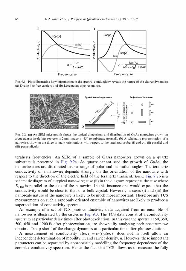
Fig. 9.2. (a) An SEM micrograph shows the typical dimensions and distribution of GaAs nanowires grown on
z-cut quartz (scale bar represents 2 mm, image at 451 to substrate normal). (b) A schematic representation of a
nanowire, showing the three primary orientations with respect to the terahertz probe: (i) end on, (ii) parallel and
(iii) perpendicular.
Fig. 9.1. Plots illustrating how information in the spectral conductivity reveals the nature of the charge dynamics:
(a) Drude-like free-carriers and (b) Lorentzian type resonance.
H.J. Joyce et al. / Progress in Quantum Electronics 35 (2011) 23–7566
terahertz frequencies. An SEM of a sample of GaAs nanowires grown on a quartzsubstrate is presented in Fig. 9.2a. As quartz cannot seed the growth of GaAs, thenanowire axes are distributed over a range of polar and azimuthal angles. The terahertzconductivity of a nanowire depends strongly on the orientation of the nanowire withrespect to the direction of the electric field of the terahertz transient, ETHz. Fig. 9.2b is aschematic diagram of a typical nanowire; case (ii) in the diagram represents the case whereETHz is parallel to the axis of the nanowire. In this instance one would expect that theconductivity would be close to that of a bulk crystal. However, in cases (i) and (iii) thenanoscale nature of the nanowire is likely to be much more important. Therefore any TCSmeasurements on such a randomly oriented ensemble of nanowires are likely to produce asuperposition of conductivity spectra.An example of a set of TCS photoconductivity data acquired from an ensemble of
nanowires is illustrated by the circles in Fig. 9.3. The TCS data consist of a conductivityspectrum at particular delay times after photoexcitation. In this case the spectra at 50, 350,500, 650 and 1200 fs after photoexcitation are shown. By analysing each spectrum weobtain a ‘‘snap-shot’’ of the charge dynamics at a particular time after photoexcitation.A measurement of conductivity sðo; tÞ ¼ enðtÞmðo; tÞ does not in itself allow an
independent determination of mobility, m, and carrier density, n. However, these importantparameters can be separated by appropriately modelling the frequency dependence of thecomplex conductivity spectrum. Hence the fact that TCS allows us to measure the fully
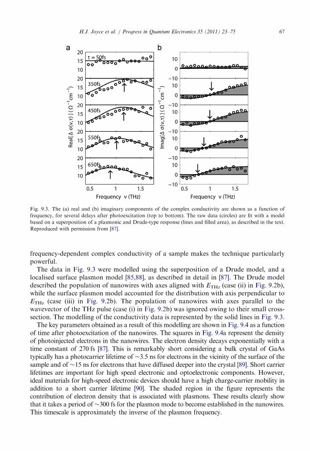
Fig. 9.3. The (a) real and (b) imaginary components of the complex conductivity are shown as a function of
frequency, for several delays after photoexcitation (top to bottom). The raw data (circles) are fit with a model
based on a superposition of a plasmonic and Drude-type response (lines and filled area), as described in the text.
Reproduced with permission from [87].
H.J. Joyce et al. / Progress in Quantum Electronics 35 (2011) 23–75 67
frequency-dependent complex conductivity of a sample makes the technique particularlypowerful.
The data in Fig. 9.3 were modelled using the superposition of a Drude model, and alocalised surface plasmon model [85,88], as described in detail in [87]. The Drude modeldescribed the population of nanowires with axes aligned with ETHz (case (ii) in Fig. 9.2b),while the surface plasmon model accounted for the distribution with axis perpendicular toETHz (case (iii) in Fig. 9.2b). The population of nanowires with axes parallel to thewavevector of the THz pulse (case (i) in Fig. 9.2b) was ignored owing to their small cross-section. The modelling of the conductivity data is represented by the solid lines in Fig. 9.3.
The key parameters obtained as a result of this modelling are shown in Fig. 9.4 as a functionof time after photoexcitation of the nanowires. The squares in Fig. 9.4a represent the densityof photoinjected electrons in the nanowires. The electron density decays exponentially with atime constant of 270 fs [87]. This is remarkably short considering a bulk crystal of GaAstypically has a photocarrier lifetime of �3.5 ns for electrons in the vicinity of the surface of thesample and of �15 ns for electrons that have diffused deeper into the crystal [89]. Short carrierlifetimes are important for high speed electronic and optoelectronic components. However,ideal materials for high-speed electronic devices should have a high charge-carrier mobility inaddition to a short carrier lifetime [90]. The shaded region in the figure represents thecontribution of electron density that is associated with plasmons. These results clearly showthat it takes a period of�300 fs for the plasmon mode to become established in the nanowires.This timescale is approximately the inverse of the plasmon frequency.
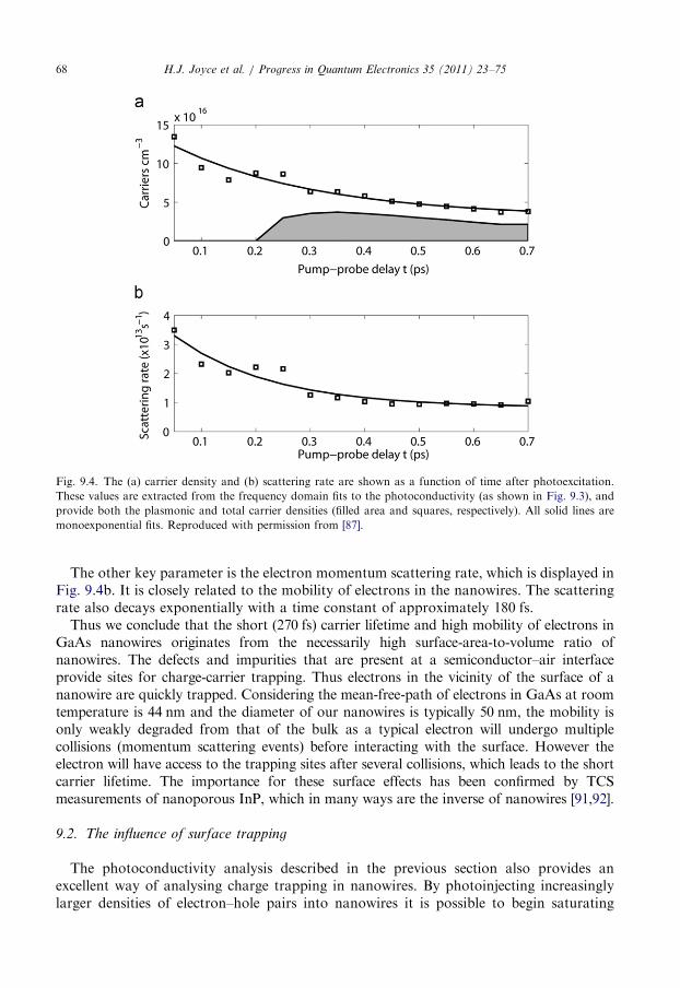
Fig. 9.4. The (a) carrier density and (b) scattering rate are shown as a function of time after photoexcitation.
These values are extracted from the frequency domain fits to the photoconductivity (as shown in Fig. 9.3), and
provide both the plasmonic and total carrier densities (filled area and squares, respectively). All solid lines are
monoexponential fits. Reproduced with permission from [87].
H.J. Joyce et al. / Progress in Quantum Electronics 35 (2011) 23–7568
The other key parameter is the electron momentum scattering rate, which is displayed inFig. 9.4b. It is closely related to the mobility of electrons in the nanowires. The scatteringrate also decays exponentially with a time constant of approximately 180 fs.Thus we conclude that the short (270 fs) carrier lifetime and high mobility of electrons in
GaAs nanowires originates from the necessarily high surface-area-to-volume ratio ofnanowires. The defects and impurities that are present at a semiconductor–air interfaceprovide sites for charge-carrier trapping. Thus electrons in the vicinity of the surface of ananowire are quickly trapped. Considering the mean-free-path of electrons in GaAs at roomtemperature is 44 nm and the diameter of our nanowires is typically 50 nm, the mobility isonly weakly degraded from that of the bulk as a typical electron will undergo multiplecollisions (momentum scattering events) before interacting with the surface. However theelectron will have access to the trapping sites after several collisions, which leads to the shortcarrier lifetime. The importance for these surface effects has been confirmed by TCSmeasurements of nanoporous InP, which in many ways are the inverse of nanowires [91,92].
9.2. The influence of surface trapping
The photoconductivity analysis described in the previous section also provides anexcellent way of analysing charge trapping in nanowires. By photoinjecting increasinglylarger densities of electron–hole pairs into nanowires it is possible to begin saturating
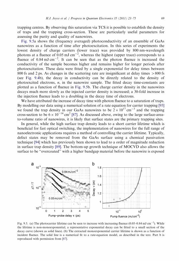
H.J. Joyce et al. / Progress in Quantum Electronics 35 (2011) 23–75 69
trapping centres. By observing this saturation via TCS it is possible to establish the densityof traps and the trapping cross-section. These are particularly useful parameters forassessing the purity and quality of nanowires.
Fig. 9.5a shows the (frequency averaged) photoconductivity of an ensemble of GaAsnanowires as a function of time after photoexcitation. In this series of experiments thelowest density of charge carriers (lower trace) was provided by 800 nm-wavelengthphotons at a fluence of 0.05 mJ cm�2, whereas the highest (upper trace) corresponds to afluence of 0.84 mJ cm�2. It can be seen that as the photon fluence is increased theconductivity of the sample becomes higher and remains higher for longer periods afterphotoexcitation. These data were fitted by a single exponential for delay times between800 fs and 2 ps. As changes in the scattering rate are insignificant at delay times 4800 fs(see Fig. 9.4b), the decay in conductivity can be directly related to the density ofphotoexcited electrons, n, in the nanowire sample. The fitted decay time-constants areplotted as a function of fluence in Fig. 9.5b. The charge carrier density in the nanowiresdecays much more slowly as the injected carrier density is increased; a 30-fold increase inthe injection fluence leads to a doubling in the decay time of electrons.
We have attributed the increase of decay time with photon fluence to a saturation of traps.By modelling our data using a numerical solution of a rate equation for carrier trapping [93]we found the trap density in our GaAs nanowires to be 2� 1017 cm�3 and the trappingcross-section to be 6� 10�14 cm2 [87]. As discussed above, owing to the large surface-area-to-volume ratio of nanowires, it is likely that surface states are the primary trapping sites.
In general, while the high surface trap density leads to a short carrier lifetime which isbeneficial for fast optical switching, the implementation of nanowires for the full range ofnanoelectronic applications requires a method of controlling the carrier lifetime. Typically,defect states may be removed from the GaAs surface using a chemical passivationtechnique [94] which has previously been shown to lead to a order of magnitude reductionin surface trap density [89]. The bottom-up growth technique of MOCVD also allows thesurface to be ‘‘overcoated’’ with a higher bandgap material before the nanowire is exposed
Fig. 9.5. (a) The photocarrier lifetime can be seen to increase with increasing fluence (0.05–0.84 mJ cm�2). While
the lifetime is non-monoexponential, a representative exponential decay can be fitted to a small section of the
decay curve (shown as solid lines). (b) The extracted monoexponential carrier lifetime is shown as a function of
incident fluence. The solid line is a numerical fit to a rate-equation model, as described in the text. Part b is
reproduced with permission from [87].
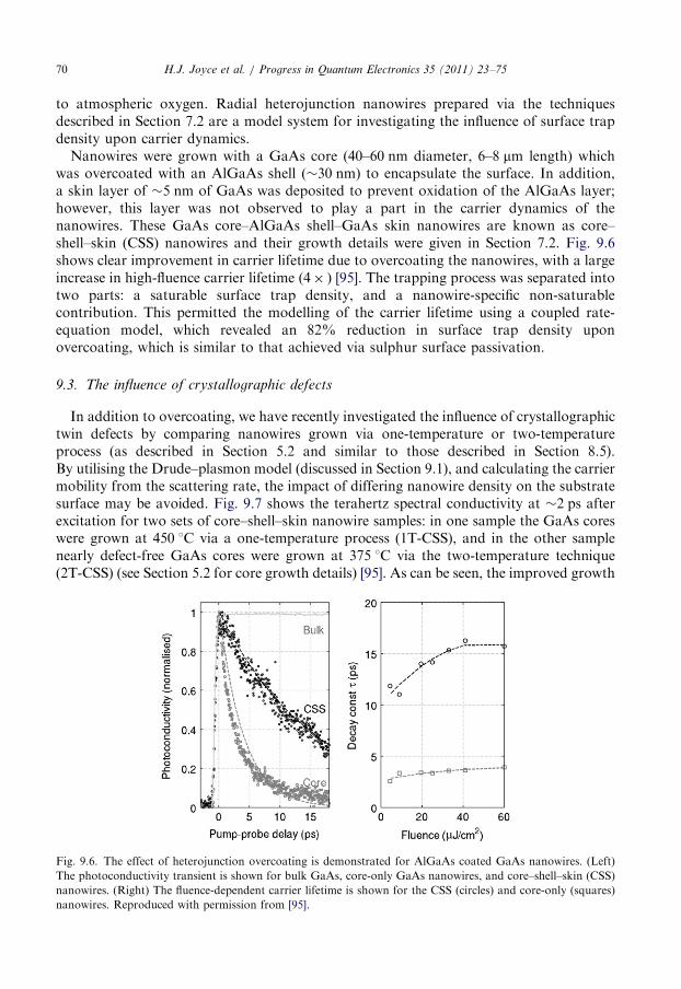
H.J. Joyce et al. / Progress in Quantum Electronics 35 (2011) 23–7570
to atmospheric oxygen. Radial heterojunction nanowires prepared via the techniquesdescribed in Section 7.2 are a model system for investigating the influence of surface trapdensity upon carrier dynamics.Nanowires were grown with a GaAs core (40–60 nm diameter, 6–8 mm length) which
was overcoated with an AlGaAs shell (�30 nm) to encapsulate the surface. In addition,a skin layer of �5 nm of GaAs was deposited to prevent oxidation of the AlGaAs layer;however, this layer was not observed to play a part in the carrier dynamics of thenanowires. These GaAs core–AlGaAs shell–GaAs skin nanowires are known as core–shell–skin (CSS) nanowires and their growth details were given in Section 7.2. Fig. 9.6shows clear improvement in carrier lifetime due to overcoating the nanowires, with a largeincrease in high-fluence carrier lifetime (4� ) [95]. The trapping process was separated intotwo parts: a saturable surface trap density, and a nanowire-specific non-saturablecontribution. This permitted the modelling of the carrier lifetime using a coupled rate-equation model, which revealed an 82% reduction in surface trap density uponovercoating, which is similar to that achieved via sulphur surface passivation.
9.3. The influence of crystallographic defects
In addition to overcoating, we have recently investigated the influence of crystallographictwin defects by comparing nanowires grown via one-temperature or two-temperatureprocess (as described in Section 5.2 and similar to those described in Section 8.5).By utilising the Drude–plasmon model (discussed in Section 9.1), and calculating the carriermobility from the scattering rate, the impact of differing nanowire density on the substratesurface may be avoided. Fig. 9.7 shows the terahertz spectral conductivity at �2 ps afterexcitation for two sets of core–shell–skin nanowire samples: in one sample the GaAs coreswere grown at 450 1C via a one-temperature process (1T-CSS), and in the other samplenearly defect-free GaAs cores were grown at 375 1C via the two-temperature technique(2T-CSS) (see Section 5.2 for core growth details) [95]. As can be seen, the improved growth
Fig. 9.6. The effect of heterojunction overcoating is demonstrated for AlGaAs coated GaAs nanowires. (Left)
The photoconductivity transient is shown for bulk GaAs, core-only GaAs nanowires, and core–shell–skin (CSS)
nanowires. (Right) The fluence-dependent carrier lifetime is shown for the CSS (circles) and core-only (squares)
nanowires. Reproduced with permission from [95].
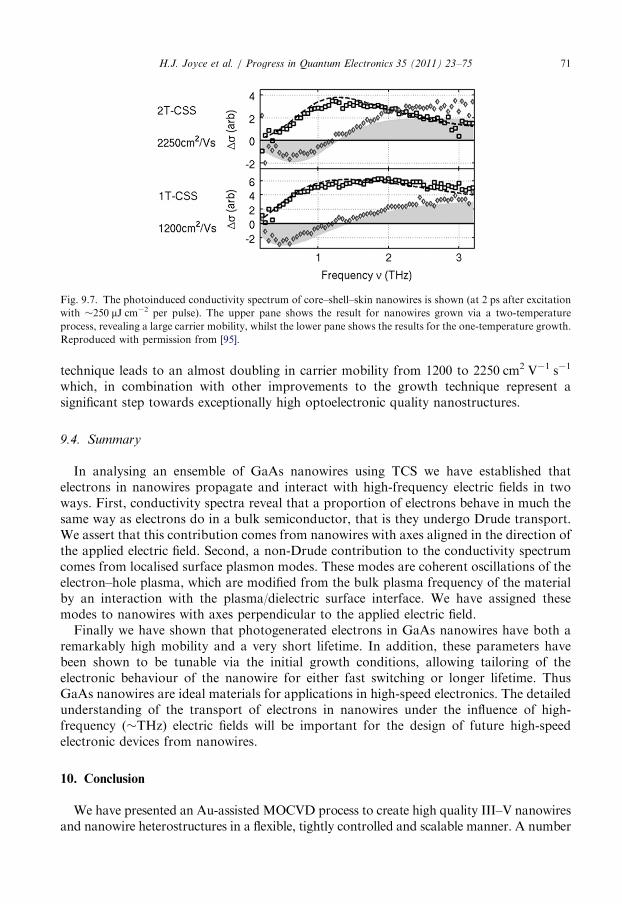
Fig. 9.7. The photoinduced conductivity spectrum of core–shell–skin nanowires is shown (at 2 ps after excitation
with �250 mJ cm�2 per pulse). The upper pane shows the result for nanowires grown via a two-temperature
process, revealing a large carrier mobility, whilst the lower pane shows the results for the one-temperature growth.
Reproduced with permission from [95].
H.J. Joyce et al. / Progress in Quantum Electronics 35 (2011) 23–75 71
technique leads to an almost doubling in carrier mobility from 1200 to 2250 cm2 V�1 s�1
which, in combination with other improvements to the growth technique represent asignificant step towards exceptionally high optoelectronic quality nanostructures.
9.4. Summary
In analysing an ensemble of GaAs nanowires using TCS we have established thatelectrons in nanowires propagate and interact with high-frequency electric fields in twoways. First, conductivity spectra reveal that a proportion of electrons behave in much thesame way as electrons do in a bulk semiconductor, that is they undergo Drude transport.We assert that this contribution comes from nanowires with axes aligned in the direction ofthe applied electric field. Second, a non-Drude contribution to the conductivity spectrumcomes from localised surface plasmon modes. These modes are coherent oscillations of theelectron–hole plasma, which are modified from the bulk plasma frequency of the materialby an interaction with the plasma/dielectric surface interface. We have assigned thesemodes to nanowires with axes perpendicular to the applied electric field.
Finally we have shown that photogenerated electrons in GaAs nanowires have both aremarkably high mobility and a very short lifetime. In addition, these parameters havebeen shown to be tunable via the initial growth conditions, allowing tailoring of theelectronic behaviour of the nanowire for either fast switching or longer lifetime. ThusGaAs nanowires are ideal materials for applications in high-speed electronics. The detailedunderstanding of the transport of electrons in nanowires under the influence of high-frequency (�THz) electric fields will be important for the design of future high-speedelectronic devices from nanowires.
10. Conclusion
We have presented an Au-assisted MOCVD process to create high quality III–V nanowiresand nanowire heterostructures in a flexible, tightly controlled and scalable manner. A number
H.J. Joyce et al. / Progress in Quantum Electronics 35 (2011) 23–7572
of characterisation techniques have been presented, including electron microscopy, PL andTCS. Each of these techniques complements the others, and provides crucial informationabout the bandgap, carrier transport and optical properties of the nanowires. For instance,the presence of ZB/WZ polytypism within nanowire samples is determined by TEM, and thenPL measurements reveal its major effect on nanowire optical properties. Nanowire propertiescan be carefully tuned during growth. For instance, we can grow bare GaAs nanowires withhigh mobility and very short carrier lifetime, which makes them ideal for high-speedelectronics. On the other hand, when grown to be twin-free and clad in an AlGaAs shell,GaAs nanowires have a significantly enhanced lifetime, which makes them suitable for opticaldevices such as solar cells and photodetectors. These advances will enable a wide range ofhigh performance nanowire-based quantum electronic and optoelectronic devices.
Acknowledgements
We wish to thank our collaborators at the Australian National University (JenniferWong-Leung, Jung Hyun Kang, Suriati Paiman and Timothy Burgess), the University ofQueensland (Mohanchand Paladugu, Xin Zhang, Yanan Guo), the University ofCincinnati (Thang Ba Hoang, Lyuba Titova, Melodie Fickenscher, Saranga Perera,Mohammad Montazeri) and the University of Oxford (Laura Herz). We thank theAustralian Research Council, the National Science Foundation (Grants ECCS-0701703and DMR-0806700), the Korean Science and Engineering Foundation (Grant F01-2007-000-10087-0) and the Engineering and Physical Sciences Research Council for financialsupport. The Australian National Fabrication Facility established under the AustralianGovernment’s National Collaborative Research Infrastructure Strategy, is gratefullyacknowledged for providing access to the facilities used in this research.
References
[1] F. Patolsky, G. Zheng, O. Hayden, M. Lakadamyali, X. Zhuang, C.M. Lieber, Proc. Natl. Acad. Sci. USA
101 (2004) 14017–14022.
[2] J.-I. Hahm, C.M. Lieber, Nano Lett. 4 (2004) 51–54.
[3] D.J. Sirbuly, A. Tao, M. Law, R. Fan, P. Yang, Adv. Mater. 19 (2007) 61–66.
[4] E.D. Minot, F. Kelkensberg, M. van Kouwen, J.A. van Dam, L.P. Kouwenhoven, V. Zwiller, M.T. Borgstrom,
O. Wunnicke, M.A. Verheijen, E.P.A.M. Bakkers, Nano Lett. 7 (2007) 367–371.
[5] Y. Huang, X. Duan, Charles M. Lieber, Small 1 (2005) 142–147.
[6] F. Qian, S. Gradecak, Y. Li, C.-Y. Wen, C.M. Lieber, Nano Lett. 5 (2005) 2287–2291.
[7] Y. Dong, B. Tian, T.J. Kempa, C.M. Lieber, Nano Lett. 9 (2009) 2183–2187.
[8] B. Tian, X. Zheng, T.J. Kempa, Y. Fang, N. Yu, G. Yu, J. Huang, C.M. Lieber, Nature 449 (2007) 885–889.
[9] J.A. Czaban, D.A. Thompson, R.R. LaPierre, Nano Lett. 9 (2009) 148–154.
[10] Y. Xia, P. Yang, Y. Sun, Y. Wu, B. Mayers, B. Gates, Y. Yin, F. Kim, H. Yan, Adv. Mater. 15 (2003)
353–389.
[11] R.S. Wagner, W.C. Ellis, Appl. Phys. Lett. 4 (1964) 89–90.
[12] P.D. Markowitz, M.P. Zach, P.C. Gibbons, R.M. Penner, W.E. Buhro, J. Am. Chem. Soc. 123 (2001)
4502–4511.
[13] M.A. Verheijen, G. Immink, T. de Smet, M.T. Borgstrom, E.P.A.M. Bakkers, J. Am. Chem. Soc. 128 (2006)
1353–1359.
[14] K. Hiruma, M. Yazawa, K. Haraguchi, K. Ogawa, T. Katsuyama, M. Koguchi, H. Kakibayashi, J. Appl.
Phys. 74 (1993) 3162–3171.
[15] K.A. Dick, K. Deppert, T. Martensson, B. Mandl, L. Samuelson, W. Seifert, Nano Lett. 5 (2005) 761–764.
[16] X. Duan, J. Wang, C.M. Lieber, Appl. Phys. Lett. 76 (2000) 1116–1118.
H.J. Joyce et al. / Progress in Quantum Electronics 35 (2011) 23–75 73
[17] J.C. Harmand, M. Tchernycheva, G. Patriarche, L. Travers, F. Glas, G. Cirlin, J. Cryst. Growth 301–302
(2007) 853–856.
[18] A.I. Persson, B.J. Ohlsson, S. Jeppesen, L. Samuelson, J. Cryst. Growth 272 (2004) 167–174.
[19] K. Hiruma, H. Murakoshi, M. Yazawa, T. Katsuyama, J. Cryst. Growth 163 (1996) 226–231.
[20] W. Seifert, M. Borgstrom, K. Deppert, K.A. Dick, J. Johansson, M.W. Larsson, T. Martensson, N. Skold,
C.P.T. Svensson, B.A. Wacaser, L.R. Wallenberg, L. Samuelson, J. Cryst. Growth 272 (2004) 211–220.
[21] G.B. Stringfellow, Organometallic Vapor-Phase Epitaxy: Theory and Practice, Academic Press, San Diego,
1999.
[22] K.A. Dick, Prog. Cryst. Growth Charact. Mater. 54 (2008) 138–173.
[23] S.E.R. Hiscocks, W. Hume-Rothery, Proc. R. Soc. London A 282 (1964) 318–330.
[24] J. Murray, H. Okamoto, T. Massalski, J. Phase Equilibria 8 (1987) 20–30.
[25] H. Okamoto, J. Phase Equilibria 25 (2004) 197–198.
[26] R. Elliott, F. Shunk, J. Phase Equilibria 2 (1981) 356–358.
[27] H. Okamoto, T. Massalski, J. Phase Equilibria 5 (1984) 166–171.
[28] H. Okamoto, T. Massalski, J. Phase Equilibria 5 (1984) 490–491.
[29] H. Okamoto, T. Massalski, J. Phase Equilibria 5 (1984) 56–59.
[30] C.T. Tsai, R.S. Williams, J. Mater. Res. 1 (1986) 820–826.
[31] C.T. Tsai, R.S. Williams, J. Mater. Res. 1 (1986) 352–360.
[32] C. Chatillon, F. Hodaj, A. Pisch, J. Cryst. Growth 311 (2009) 3598–3608.
[33] K.A. Dick, K. Deppert, L.S. Karlsson, L.R. Wallenberg, L. Samuelson, W. Seifert, Adv. Funct. Mater.
15 (2005) 1603–1610.
[34] M. Tchernycheva, J.C. Harmand, G. Patriarche, L. Travers, G.E. Cirlin, Nanotechnology 17 (2006) 4025.
[35] M. Tchernycheva, L. Travers, G. Patriarche, F. Glas, J.-C. Harmand, G.E. Cirlin, V.G. Dubrovskii, J. Appl.
Phys. 102 (2007) 094313.
[36] A.I. Persson, M.W. Larsson, S. Stenstrom, B.J. Ohlsson, L. Samuelson, L.R. Wallenberg, Nat. Mater.
3 (2004) 677–681.
[37] J.C. Harmand, G. Patriarche, N. Pere-Laperne, M.-N. Merat-Combes, L. Travers, F. Glas, Appl. Phys. Lett.
87 (2005) 203101.
[38] G.A. Bootsma, H.J. Gassen, J. Cryst. Growth 10 (1971) 223–234.
[39] S. Kodambaka, J. Tersoff, M.C. Reuter, F.M. Ross, Science 316 (2007) 729–732.
[40] P. Cheyssac, M. Sacilotti, G. Patriarche, J. Appl. Phys. 100 (2006) 044315.
[41] B.A. Wacaser, K.A. Dick, J. Johansson, M.T. Borgstrom, K. Deppert, L. Samuelson, Adv. Mater. 21 (2009)
153–165.
[42] J. Johansson, C.P.T. Svensson, T. Martensson, L. Samuelson, W. Seifert, J. Phys. Chem. B 109 (2005)
13567–13571.
[43] M.T. Borgstrom, G. Immink, B. Ketelaars, R.E. Algra, E.P.A.M. Bakkers, Nat. Nano 2 (2007) 541–544.
[44] S.A. Dayeh, E.T. Yu, D. Wang, Nano Lett. 9 (2009) 1967–1972.
[45] K.A. Dick, K. Deppert, L. Samuelson, W. Seifert, J. Cryst. Growth 297 (2006) 326–333.
[46] M. Mattila, T. Hakkarainen, M. Mulot, H. Lipsanen, Nanotechnology 17 (2006) 1580.
[47] F. Glas, J.C. Harmand, G. Patriarche, Phys. Rev. Lett. 99 (2007) 146101.
[48] J. Zou, M. Paladugu, H. Wang, G.J. Auchterlonie, Y. Guo, Y. Kim, Q. Gao, H.J. Joyce, H.H. Tan,
C. Jagadish, Small 3 (2007) 389–393.
[49] J. Johansson, L.S. Karlsson, C.P.T. Svensson, T. Martensson, B.A. Wacaser, K. Deppert, L. Samuelson,
W. Seifert, Nat. Mater. 5 (2006) 574–580.
[50] M.A. Verheijen, R.E. Algra, M.T. Borgstrom, G. Immink, E. Sourty, W.J.P. van Enckevort, E. Vlieg,
E.P.A.M. Bakkers, Nano Lett. 7 (2007) 3051–3055.
[51] H.J. Joyce, Q. Gao, H.H. Tan, C. Jagadish, Y. Kim, X. Zhang, Y. Guo, J. Zou, Nano Lett. 7 (2007) 921–926.
[52] H.J. Joyce, Q. Gao, H.H. Tan, C. Jagadish, Y. Kim, M.A. Fickenscher, S. Perera, T.B. Hoang, L.M. Smith,
H.E. Jackson, J.M. Yarrison-Rice, X. Zhang, J. Zou, Adv. Funct. Mater. 18 (2008) 3794–3800.
[53] H.J. Joyce, Q. Gao, H.H. Tan, C. Jagadish, Y. Kim, M.A. Fickenscher, S. Perera, T.B. Hoang, L.M. Smith,
H.E. Jackson, J.M. Yarrison-Rice, X. Zhang, J. Zou, Nano Lett. 9 (2009) 695–701.
[54] J. Vesenka, S. Manne, R. Giberson, T. Marsh, E. Henderson, Biophys. J. 65 (1993) 992–997.
[55] J.H. Woodruff, J.B. Ratchford, I.A. Goldthorpe, P.C. McIntyre, C.E.D. Chidsey, Nano Lett. 7 (2007)
1637–1642.
[56] S. Perera, M.A. Fickenscher, H.E. Jackson, L.M. Smith, J.M. Yarrison-Rice, H.J. Joyce, Q. Gao, H.H. Tan,
C. Jagadish, X. Zhang, J. Zou, Appl. Phys. Lett. 93 (2008) 053110.
H.J. Joyce et al. / Progress in Quantum Electronics 35 (2011) 23–7574
[57] S. Paiman, Q. Gao, H.H. Tan, C. Jagadish, K. Pemasiri, M. Montazeri, H.E. Jackson, L.M. Smith,
J.M. Yarrison-rice, X. Zhang, J. Zou, Nanotechnology 20 (2009) 225606.
[58] H.J. Joyce, J. Wong-Leung, Q. Gao, H.H. Tan, C. Jagadish, Nano Lett. 10 (2010) 908–915.
[59] S.K. Lim, M.J. Tambe, M.M. Brewster, S. Gradecak, Nano Lett. 8 (2008) 1386–1392.
[60] Y. Kim, H.J. Joyce, Q. Gao, H.H. Tan, C. Jagadish, M. Paladugu, J. Zou, A.A. Suvorova, Nano Lett.
6 (2006) 599–604.
[61] Y.N. Guo, J. Zou, M. Paladugu, H. Wang, Q. Gao, H.H. Tan, C. Jagadish, Appl. Phys. Lett. 89 (2006)
231917.
[62] E. Ertekin, P.A. Greaney, D.C. Chrzan, T.D. Sands, J. Appl. Phys. 97 (2005) 114325.
[63] M. Paladugu, J. Zou, Y.-N. Guo, X. Zhang, H.J. Joyce, Q. Gao, H.H. Tan, C. Jagadish, Y. Kim, J. Appl.
Phys. 105 (2009) 073503.
[64] M. Paladugu, J. Zou, Y.-N. Guo, Graeme J. Auchterlonie, Hannah J. Joyce, Q. Gao, H.H. Tan, C. Jagadish,
Y. Kim, Small 3 (2007) 1873–1877.
[65] M. Paladugu, J. Zou, G.J. Auchterlonie, Y.N. Guo, Y. Kim, H.J. Joyce, Q. Gao, H.H. Tan, C. Jagadish,
Appl. Phys. Lett. 91 (2007) 133115.
[66] M. Paladugu, J. Zou, Y.-N. Guo, X. Zhang, Y. Kim, H.J. Joyce, Q. Gao, H.H. Tan, C. Jagadish, Appl. Phys.
Lett. 93 (2008) 101911.
[67] M. Paladugu, J. Zou, Y.-N. Guo, X. Zhang, Hannah J. Joyce, Q. Gao, H.H. Tan, C. Jagadish, Y. Kim,
Angew. Chem. 121 (2009) 794–797.
[68] M. Paladugu, J. Zou, Y. Guo, X. Zhang, H. Joyce, Q. Gao, H. Tan, C. Jagadish, Y. Kim, Nanoscale Res.
Lett. 4 (2009) 846–849.
[69] M. Paladugu, J. Zou, Y.-N. Guo, X. Zhang, H.J. Joyce, Q. Gao, H.H. Tan, C. Jagadish, Y. Kim, Appl. Phys.
Lett. 93 (2008) 201908.
[70] X. Zhang, J. Zou, M. Paladugu, Y. Guo, Y. Wang, Y. Kim, H.J. Joyce, Q. Gao, H.H. Tan, C. Jagadish,
Small 5 (2009) 366–369.
[71] M.S. Gudiksen, J. Wang, C.M. Lieber, J. Phys. Chem. B 106 (2002) 4036–4039.
[72] G. Zhang, K. Tateno, H. Sanada, T. Tawara, H. Gotoh, H. Nakano, Appl. Phys. Lett. 95 (2009) 123104.
[73] A. Mishra, L.V. Titova, T.B. Hoang, H.E. Jackson, L.M. Smith, J.M. Yarrison-Rice, Y. Kim, H.J. Joyce,
Q. Gao, H.H. Tan, C. Jagadish, Appl. Phys. Lett. 91 (2007) 263104.
[74] S. Reitzenstein, S. Munch, C. Hofmann, A. Forchel, S. Crankshaw, L.C. Chuang, M. Moewe, C. Chang-
Hasnain, Appl. Phys. Lett. 91 (2007) 091103.
[75] N. Akopian, G. Patriarche, L. Liu, J.-C. Harmand, V. Zwiller, Nano Lett. 10 (2010) 1198–1201.
[76] M.T. Borgstrom, V. Zwiller, E. Muller, A. Imamoglu, Nano Lett. 5 (2005) 1439–1443.
[77] M.H.M. van Weert, N. Akopian, U. Perinetti, M.P. van Kouwen, R.E. Algra, M.A. Verheijen,
E.P.A.M. Bakkers, L.P. Kouwenhoven, V. Zwiller, Nano Lett. 9 (2009) 1989–1993.
[78] L.V. Titova, T.B. Hoang, H.E. Jackson, L.M. Smith, J.M. Yarrison-Rice, J.L. Lensch, L.J. Lauhon,
Appl. Phys. Lett. 89 (2006) 053119.
[79] L.V. Titova, T.B. Hoang, H.E. Jackson, L.M. Smith, J.M. Yarrison-Rice, Y. Kim, H.J. Joyce, H.H. Tan,
C. Jagadish, Appl. Phys. Lett. 89 (2006) 173126.
[80] T.B. Hoang, L.V. Titova, J.M. Yarrison-Rice, H.E. Jackson, A.O. Govorov, Y. Kim, H.J. Joyce, H.H. Tan,
C. Jagadish, L.M. Smith, Nano Lett. 7 (2007) 588–595.
[81] L.M. Smith, H.E. Jackson, J.M. Yarrison-Rice, C. Jagadish, Semicond. Sci. Technol. 25 (2010) 024010.
[82] G.D. Gilliland, Mater. Sci. Eng. R: Rep. 18 (1997) 99–399.
[83] L.V. Titova, T.B. Hoang, J.M. Yarrison-Rice, H.E. Jackson, Y. Kim, H.J. Joyce, Q. Gao, H.H. Tan,
C. Jagadish, X. Zhang, J. Zou, L.M. Smith, Nano Lett. 7 (2007) 3383–3387.
[84] M. Montazeri, M. Fickenscher, L.M. Smith, H.E. Jackson, J. Yarrison-Rice, J.H. Kang, Q. Gao, H.H. Tan,
C. Jagadish, Y. Guo, J. Zou, M.-E. Pistol, C.E. Pryor, Nano Lett. 10 (2010) 880–886.
[85] H.-K. Nienhuys, V. Sundstrom, Appl. Phys. Lett. 87 (2005) 012101.
[86] R.H.M. Groeneveld, D. Grischkowsky, J. Opt. Soc. Am. B 11 (1994) 2502–2507.
[87] P. Parkinson, J. Lloyd-Hughes, Q. Gao, H.H. Tan, C. Jagadish, M.B. Johnston, L.M. Herz, Nano Lett.
7 (2007) 2162–2165.
[88] J.M. Pitarke, V.M. Silkin, E.V. Chulkov, P.M. Echenique, Rep. Prog. Phys. 70 (2007) 1–87.
[89] J. Lloyd-Hughes, S.K.E. Merchant, L. Fu, H.H. Tan, C. Jagadish, E. Castro-Camus, M.B. Johnston, Appl.
Phys. Lett. 89 (2006) 232102.
[90] E. Castro-Camus, L. Fu, J. Lloyd-Hughes, H.H. Tan, C. Jagadish, M.B. Johnston, J. Appl. Phys. 104 (2008)
053113.

H.J. Joyce et al. / Progress in Quantum Electronics 35 (2011) 23–75 75
[91] J. Lloyd-Hughes, S.K.E. Merchant, L. Sirbu, I.M. Tiginyanu, M.B. Johnston, Phys. Rev. B 78 (2008)
085320.
[92] S.K.E. Merchant, J. Lloyd-Hughes, L. Sirbu, I.M. Tiginyanu, P. Parkinson, L.M. Herz, M.B. Johnston,
Nanotechnology 19 (2008) 395704.
[93] P.U. Jepsen, W. Schairer, I.H. Libon, U. Lemmer, N.E. Hecker, M. Birkholz, K. Lips, M. Schall, Appl.
Phys. Lett. 79 (2001) 1291–1293.
[94] V.N. Bessolov, M.V. Lebedev, Semiconductors 32 (1998) 1141–1156.
[95] P. Parkinson, H.J. Joyce, Q. Gao, H.H. Tan, X. Zhang, J. Zou, C. Jagadish, L.M. Herz, M.B. Johnston,
Nano Lett. 9 (2009) 3349–3353.