Hetero junction and tandem solar cell.
17
Hetero junction and Tandem solar cell By Anish Das Roll no. -14MS60R16 MATERIALS SCIENCE CENTRE Indian Institute of Technology KHARAGPUR, 721302 - INDIA MARCH, 2015 03/16/2022 1
Transcript of Hetero junction and tandem solar cell.

04/15/2023 1
Hetero junction and Tandem solar cell
By
Anish Das
Roll no. -14MS60R16
MATERIALS SCIENCE CENTRE
Indian Institute of Technology
KHARAGPUR, 721302 - INDIA
MARCH, 2015

04/15/2023 2
Overviews
What is homo junction and hetero junction?
Some idea about hetero junction. Advantages of tandem solar cell. General structure of tandem solar cell. Drawback and recent advancements.

04/15/2023 3
What is homo junction and heterojunction?
Basically we all now that solar cell is nothing but a p-n / p-p / n-n / n-p /n-i-p/p-i-n junction kind of structures.
Now if the whole junction is made of the a single material the junction is called homo junction.
But if the junction is made of different kind of materials then the junction is known as hetero junction.
04/15/2023 4
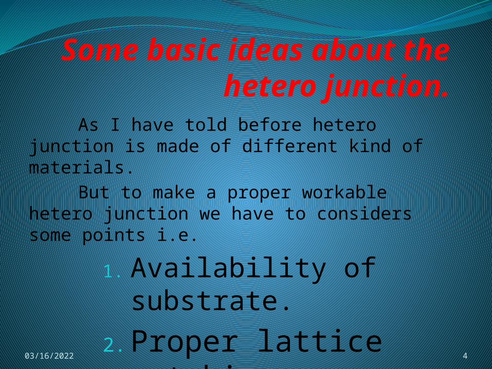
Some basic ideas about the hetero junction.
As I have told before hetero junction is made of different kind of materials.
But to make a proper workable hetero junction we have to considers some points i.e.
1. Availability of substrate.
2. Proper lattice matching.

04/15/2023 5
Availability of substratesAvailability of substrates is still a big issue
now a days. One can’t use any substrate to grow thin film or make junction on its. Some important issues are.
1. Cost issue.
2. Stability issue; though you r able to make but not stable.
Most available substrates are GaAs, InP, GaSb. They provides relatively low cost and good lattice matching.

04/15/2023 6
Proper lattice matchingYou can’t grow any thin film on any available substrate.
Cause in between substrate and film there should be lattice matching. If not then the interface will not be smooth and will act as recombination center.
You can grow any composition of composition of Al(x)Ga(1-x)As on GaAs substarte cause lattice parameter of AlAs(5.6611) and GaAs(5.6532) almost matches.
You can only grow on InP substrate. Cause only for that composition lattice parameters matches with InP
04/15/2023 7
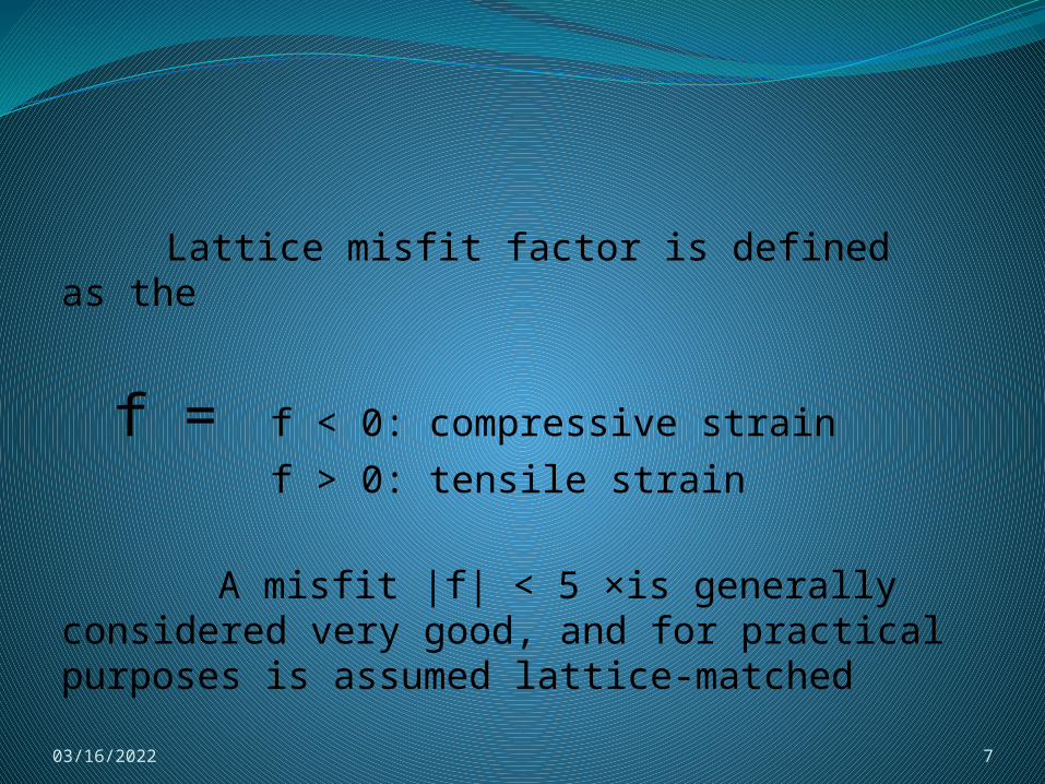
Lattice misfit factor is defined as the
f = f < 0: compressive strain
f > 0: tensile strain
A misfit |f| < 5 ×is generally considered very good, and for practical purposes is assumed lattice-matched

04/15/2023 8
Competition between strain energy and chemical energy
As we now know that the grown film is always strained due the very little lattice match. And these kind of films are produced by CVD method by surface reaction process. So chemical energy is also involved here
Certainly there will be a competition between chem. Eng and strained eng.
If stained energy dominates we will get pseudomorphic film.---------requied for our case due to smooth interface
If chem. Eng. Dominates then at the interface there will be defects -----we don’t want this.

04/15/2023 9
Tandem solar cellIt’s a multi junction(i.e. more than one p-n
junction) hetero structure solar cell.
Why multi junction is needed?
For Si energy > 1.12 eV will be absorbed(i.e upto 1.1 micro meter). But what is the upper limit?
For very high eng. Radiation the electron-hole pairs will be formed very near to the surface and can’t be separated cause because.
No built in electric field to separate. And beyond the distance of minority carrier diffusion length.
So Si cant absorb the whole solar spectrum reaching to the earth.
04/15/2023 10
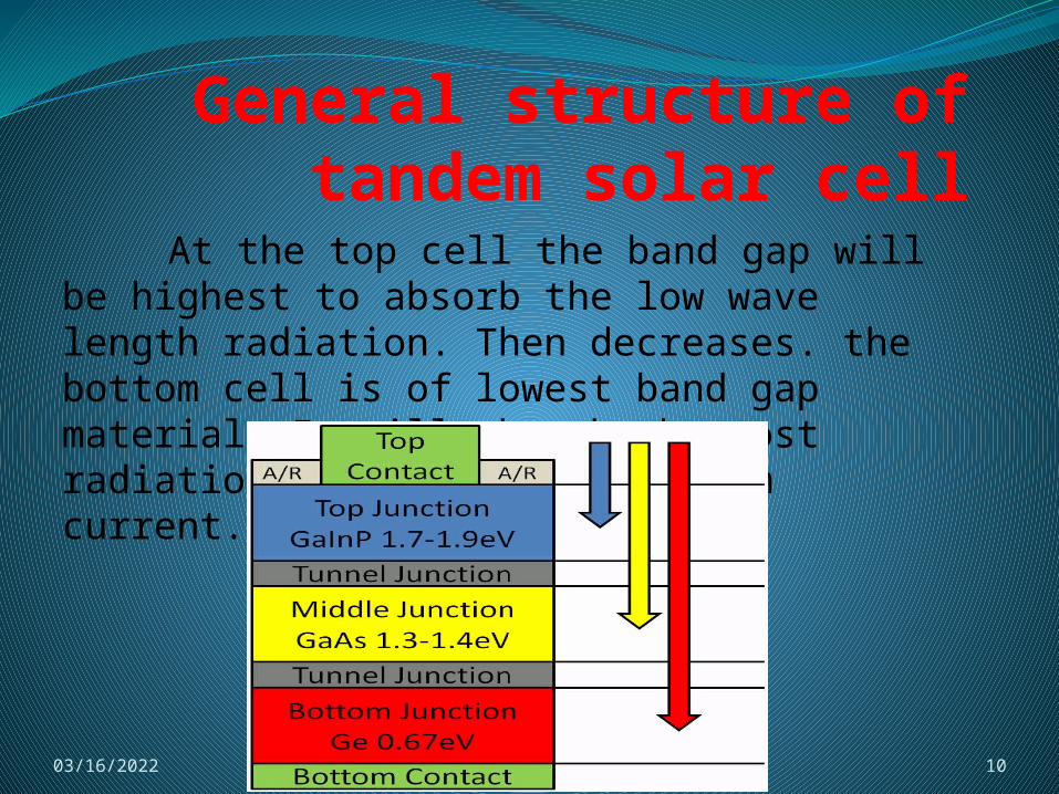
General structure of tandem solar cell
At the top cell the band gap will be highest to absorb the low wave length radiation. Then decreases. the bottom cell is of lowest band gap material. It will absorb the most radiation and gives the maximum current.

04/15/2023 11
How the cells are connected.
Let consider the above figure as the equivalent solar cell. The different resistance here signifies the different materials / junctions which will be illuminated by solar radiation. So the different cell will give different current. But we have to collect the voltage from the end and that depends on the maximum resistance or minimum current.
As our bottom cell is of lowest band gap and gives maximum current but that current may not be utilized if the others cell gives less current.

04/15/2023 12
So the cell are connected by tunnel diodes so that the junction resistance does not affects.
Tunnel DiodeIt’s a junction (may be hetero also) between
two heavily doped materials(). It allows current to flow with out almost no drop. i.e. with in a small voltage it gives large current.

04/15/2023 13
Drawback of such cell and more advancement
Bottom cell may give largest current but it can’t be utilized if any one cell gives the less current. Because will get the voltage corresponding to the lowest current.
So peoples are changing the middle cell by Q-well or Q-dot.
04/15/2023 14
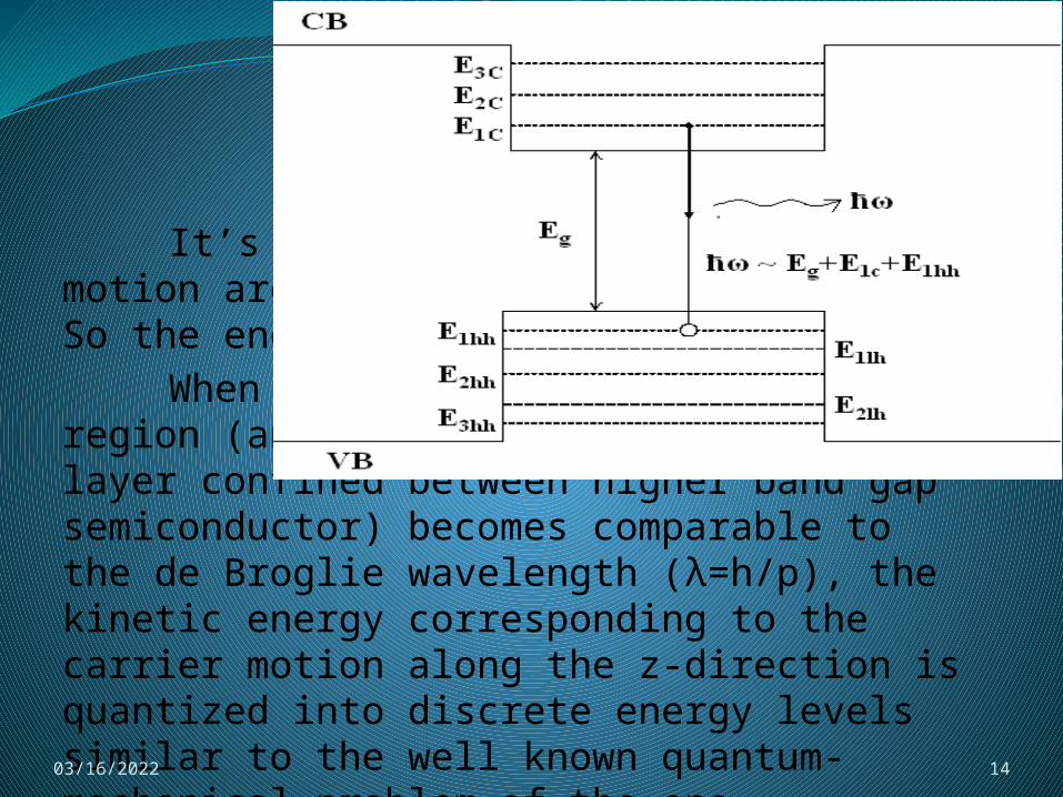
Quantum wellIt’s a 2D structure. Electrons’ motion are
confined in two directions. So the energy levels are quantized.
When the thickness of the active region (any low band gap semiconductor layer confined between higher band gap semiconductor) becomes comparable to the de Broglie wavelength (λ=h/p), the kinetic energy corresponding to the carrier motion along the z-direction is quantized into discrete energy levels similar to the well known quantum-mechanical problem of the one-dimensional potential well.--GaAS(well)/AlGaAs(barrier)
04/15/2023 15
Ready to illuminate your purpose.

04/15/2023 16

04/15/2023 17