Hetero Structures
11
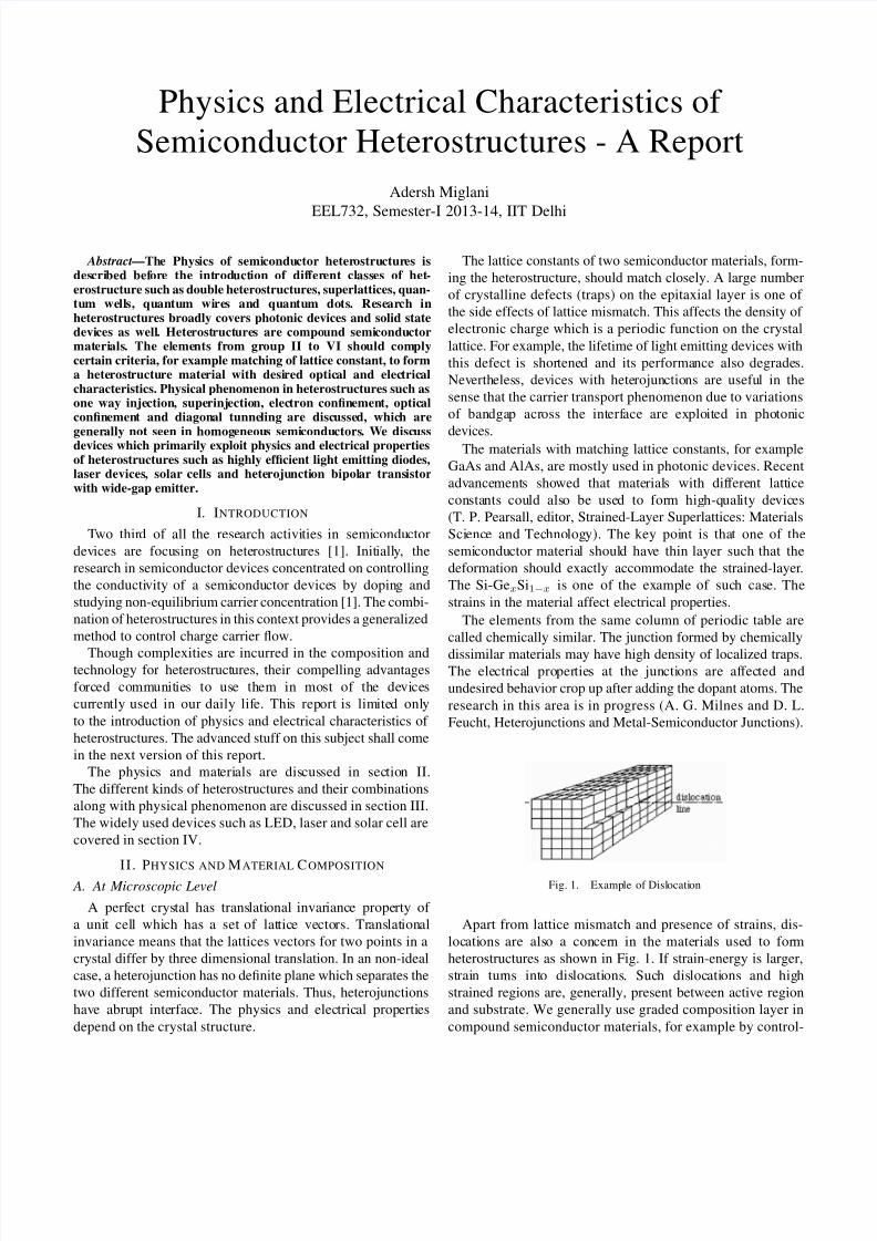
Physics and Electrical Characteristics of Semiconductor Heterostructures - A Report Adersh Miglani EEL732, Semester-I 2013-14, IIT Delhi Abstract —Th e Phys ics of semi condu ctor heterostru ctur es is des cri bed bef or e the int rod uct ion of dif fer ent cl ass es of het - erostructure such as double heterostructures, superlattices, quan- tum we ll s, quantum wi re s and quantum dots. Re se arch in heterostructures broadly covers photonic devices and solid state devices as well . Hete rost ruct ure s are compo und semi condu ctor mat eri als . The el eme nts fr om gr oup II to VI should comply certain criteria, for example matching of lattice constant, to form a hete rost ructure mate rial with desi red optic al and elec tric al characteristics. Physical phenomenon in heterostructures such as one way inje ction , supe rinj ectio n, elec tron confin emen t, optic al confin emen t and diagonal tunne ling are disc usse d, whic h are gener ally not seen in homog eneou s semi condu ctors. We disc uss devices which primarily exploit physics and electrical properties of heterostructures such as highly efficient light emitting diodes, laser devices , solar cells and hete roju ncti on bipol ar trans istor with wide-gap emitter. I. I NTRODUCTION T wo thir d of all the rese arch activities in semi condu ctor dev ices are focu sing on hete rostr uctu res [1]. Init iall y , the research in semiconductor devices concentrated on controlling the conducti vity of a semi condu ctor device s by dopin g and studying non-equilibrium carrier concentration [1]. The combi- nation of heterostructures in this context provides a generalized method to control charge carrier flow. Though complexities are incurred in the composition and technology for heterostructures, their compelling advantages forc ed communities to use them in most of the devi ce s curren tly used in our daily lif e. Thi s rep ort is limite d onl y to the introduction of physics and electrical characteristics of heterostructures. The advanced stuff on this subject shall come in the next version of this report. The phy sic s and mat eri als are dis cus sed in sec tio n II. The different kinds of heterostructures and their combinations along with physical phenomenon are discussed in section III. The widely used devices such as LED, laser and solar cell are covered in section IV. II. PHYSICS AND MATERIAL C OMPOSITION A. At Microscopic Level A perf ect crys tal has trans lati onal invar ianc e property of a uni t cel l whi ch has a set of lat tic e ve cto rs. Tr ans lat ion al invariance means that the lattices vectors for two points in a crystal differ by three dimensional translation. In an non-ideal case, a heterojunction has no definite plane which separates the two different semiconductor materials. Thus, heterojunctions hav e abrupt inte rfac e. The phys ics and elec tric al properti es depend on the crystal structure. The lattice constants of two semiconductor materials, form- ing the heterostructure, should match closely. A large number of crystalline defects (traps) on the epitaxial layer is one of the side effects of lattice mismatch. This affects the density of electronic charge which is a periodic function on the crystal lattice. For example, the lifetime of light emitting devices with this defect is shor tened and its performa nce also degrade s. Nev erth eles s, dev ices with hete rojun ctio ns are usefu l in the sense that the carrier transport phenomenon due to variations of ban dga p acr oss the int erf ace are explo it ed in pho ton ic devices. The materials with matching lattice constants, for example GaAs and AlAs, are mostly used in photonic devices. Recent adv ance ment s sho wed that mate rial s with dif fere nt latt ice consta nts could als o be use d to for m hig h-q ual ity de vices (T. P. Pearsall, editor, Strained-Layer Superlattices: Materials Sci enc e and Tec hno logy). The key point is tha t one of the semi condu ctor materia l shoul d hav e thin layer such that the deformation should exactly accommodate the strained-layer . The Si-Ge x Si 1−x is one of the examp le of suc h cas e. The strains in the material affect electrical properties. The elements from the same column of periodic table are called chemically similar. The junction formed by chemically dissimilar materials may have high density of localized traps. The ele ctr ica l pro per ties at the jun cti ons are af fec ted and undesired behavior crop up after adding the dopant atoms. The research in this area is in progress (A. G. Milnes and D. L. Feucht, Heterojunctions and Metal-Semiconductor Junctions). Fig. 1. Examp le of Dislocation Apart from lattice mismatch and presence of strains, dis- loc ati ons are als o a concer n in the mate ria ls use d to for m heterostructures as shown in Fig. 1. If strain-energy is larger, st rai n tur ns int o dis loc ati ons. Such dislocati ons and hig h strained regions are, generally, present between active region and substrate. We generally use graded composition layer in compound semiconductor materials, for example by control-
Transcript of Hetero Structures
8/11/2019 Hetero Structures
http://slidepdf.com/reader/full/hetero-structures 1/11
Physics and Electrical Characteristics of
Semiconductor Heterostructures - A Report
Adersh Miglani
EEL732, Semester-I 2013-14, IIT Delhi
Abstract—The Physics of semiconductor heterostructures isdescribed before the introduction of different classes of het-erostructure such as double heterostructures, superlattices, quan-tum wells, quantum wires and quantum dots. Research inheterostructures broadly covers photonic devices and solid statedevices as well. Heterostructures are compound semiconductormaterials. The elements from group II to VI should complycertain criteria, for example matching of lattice constant, to forma heterostructure material with desired optical and electricalcharacteristics. Physical phenomenon in heterostructures such asone way injection, superinjection, electron confinement, opticalconfinement and diagonal tunneling are discussed, which are
generally not seen in homogeneous semiconductors. We discussdevices which primarily exploit physics and electrical propertiesof heterostructures such as highly efficient light emitting diodes,laser devices, solar cells and heterojunction bipolar transistorwith wide-gap emitter.
I. INTRODUCTION
Two third of all the research activities in semiconductor
devices are focusing on heterostructures [1]. Initially, the
research in semiconductor devices concentrated on controlling
the conductivity of a semiconductor devices by doping and
studying non-equilibrium carrier concentration [1]. The combi-
nation of heterostructures in this context provides a generalized
method to control charge carrier flow.
Though complexities are incurred in the composition andtechnology for heterostructures, their compelling advantages
forced communities to use them in most of the devices
currently used in our daily life. This report is limited only
to the introduction of physics and electrical characteristics of
heterostructures. The advanced stuff on this subject shall come
in the next version of this report.
The physics and materials are discussed in section II.
The different kinds of heterostructures and their combinations
along with physical phenomenon are discussed in section III.
The widely used devices such as LED, laser and solar cell are
covered in section IV.
I I . PHYSICS AND M ATERIAL C OMPOSITION A. At Microscopic Level
A perfect crystal has translational invariance property of
a unit cell which has a set of lattice vectors. Translational
invariance means that the lattices vectors for two points in a
crystal differ by three dimensional translation. In an non-ideal
case, a heterojunction has no definite plane which separates the
two different semiconductor materials. Thus, heterojunctions
have abrupt interface. The physics and electrical properties
depend on the crystal structure.
The lattice constants of two semiconductor materials, form-
ing the heterostructure, should match closely. A large number
of crystalline defects (traps) on the epitaxial layer is one of
the side effects of lattice mismatch. This affects the density of
electronic charge which is a periodic function on the crystal
lattice. For example, the lifetime of light emitting devices with
this defect is shortened and its performance also degrades.
Nevertheless, devices with heterojunctions are useful in the
sense that the carrier transport phenomenon due to variations
of bandgap across the interface are exploited in photonic
devices.The materials with matching lattice constants, for example
GaAs and AlAs, are mostly used in photonic devices. Recent
advancements showed that materials with different lattice
constants could also be used to form high-quality devices
(T. P. Pearsall, editor, Strained-Layer Superlattices: Materials
Science and Technology). The key point is that one of the
semiconductor material should have thin layer such that the
deformation should exactly accommodate the strained-layer.
The Si-GexSi1−x is one of the example of such case. The
strains in the material affect electrical properties.
The elements from the same column of periodic table are
called chemically similar. The junction formed by chemically
dissimilar materials may have high density of localized traps.The electrical properties at the junctions are affected and
undesired behavior crop up after adding the dopant atoms. The
research in this area is in progress (A. G. Milnes and D. L.
Feucht, Heterojunctions and Metal-Semiconductor Junctions).
Fig. 1. Example of Dislocation
Apart from lattice mismatch and presence of strains, dis-
locations are also a concern in the materials used to form
heterostructures as shown in Fig. 1. If strain-energy is larger,
strain turns into dislocations. Such dislocations and high
strained regions are, generally, present between active region
and substrate. We generally use graded composition layer in
compound semiconductor materials, for example by control-

8/11/2019 Hetero Structures
http://slidepdf.com/reader/full/hetero-structures 2/11
ling mole fraction x in AlxGa1−xAs, in between active region
and substrate.
Common Anion Rule: The compound semiconductor materi-
als are used to form heterojunctions. The pair of semiconduc-
tors generally shares a common anion element. For example,
in AlxGa1−xAs-GaAs heterojunction, As is common anion
element. It is a fact that conduction band and valence band
wave functions are derived from atomic wave functions of
cations and anions (Harrison 1980).
B. Band Diagram
The first step in modeling a semiconductor device is to
draw the band diagram. The energy band diagram is used
to compute the electrostatic potential, electric field in the
junction and charge densities at various sites of the device. The
energy levels in the band diagram are measured with respect
to the reference vacuum level (E 0). Electron affinity (χs) is
the energy required to raise an electron from conduction band
to the vacuum level. So, the conduction band edge is given by
Fig. 2. Energy Band Diagram of Uniform Semiconductor Junction
E C =
E 0 − χs
(1)
The work function (Φs) of a semiconductor is the difference
between vacuum level and Fermi level (E f ). The difference
between the conduction band minimum edge and valence
band maximum edge is termed as energy band gap ( E g). The
valence band edge can be expressed as follows
E V = E C − E g = E 0 − χs −E g (2)
A homojunction has zero conduction and zero valence
band offset. Therefore, understanding the band diagram of a
homojunction is prerequisite for that of heterostructure which
has non-zero band offset.
1) Homojunction: For a uniform semiconductor junction,the three electrical quantities - electrostatic potential, electric
field and charge density - are computed using the following
techniques,
1) The gradient in the conduction band, valence band or
intrinsic Fermi level is used to compute the electrostatic
potential.
2) Slope of conduction band, valence band or Fermi level
is proportional to the electric field. The constant of
proportionality is 1
q .
Fig. 3. Energy Band Diagram of Uniform Semiconductor Homojunction
3) The second derivative of E C , E V or E i is proportional
the charge density. The constant of proportionality is
q
s .These three techniques, as is, do not work for a heterojunc-
tion. Once, the understanding of the band diagram for uniform
semiconductor junction is clear, same is easily modified for
the heterojunctions. In the presence of electrostatic potential,
V (x), the energy of charge particle changes, say, by amount
E ,
E = −qV (x) (3)
Conduction band edge is a function of x
E C (x) = E 0 − χs − qV (x) (4)
Similarly, valence band would also be a function of x in the
junction
E V (x) = E 0 − χs − E g − qV (x) (5)
Let us consider a PN-junction with uniform semiconductor
as shown in the Fig. 3. The difference between Fermi level,
E FP , and valence band of a p-type semiconductor is δ P =E FP −E V . Similarly, for n-type semiconductor, δ N = E C −
E FN . The difference between Fermi levels is given by
E FN −E FP = E g − δ N − δ P (6)
After contact, the electron would transfer from Fermi level
to lower Fermi level until a build-in potential (V bi) is estab-
lished. The build in potential is give by the difference between
the Fermi energy levels of p-type and n-type semiconductors.
qV bi = E FN − E FP = kT logN AN D
n2
i
(7)
where N D and N A are donor and acceptor impurity concen-
tration and ni is intrinsic carrier concentration.

8/11/2019 Hetero Structures
http://slidepdf.com/reader/full/hetero-structures 3/11
2) Heterojunction: For uniform semiconductor structure,
the band slope under an electric field is same for conduction
and valence bands. Therefore, electrons and holes possess
equal but opposite force and move across the metallurgical
junction as shown in Fig. 4(a). For non-uniform semiconductor
structures, there can be different possibilities of changes in the
conduction and valence band edges at the junction. Two of
such cases are given in Fig. 4(b) and Fig. 4(c). Electric force
in the last two cases is called quasi-electric field.
Fig. 4. (a) Same slope in conduction and valence bands of a homogeneoussemiconductor. (b) Zero slope in conduction band and non-zero slop in valenceband. (c) Non-zero and different slope in conduction and valence bands.
When a heterojunction is formed between n-type and p-typesemiconductors, above equation would not be valid. First, let
us consider the high level steps to draw the band diagram of
a heterojunction (Fig. 7).
1) The Fermi levels must coincide on both sides of semi-
conductor and common Fermi level should be horizontal.
2) The vacuum level is parallel to the band edges and is
continuous every where.
3) The discontinuities are present at conduction and valence
band edge at the junction. The discontinuities in conduc-
tion band edge (E C ) and valence band edge (E V )
are not function of doping in case of non-degenerate
semiconductor.4) To draw the band diagram, the signed conduction band-
offset (±E C ) and signed valence band-offset (±E V )
are added at the metallurgical junction point.
For a heterostruture, small and capital letters are used
for materials with smaller bandgap and wider bandgap. The
detailed band diagrams of a nP-heterojunction before contact is
shown in figure 5(a) [2]. After contact, the band diagram under
thermal equilibrium is shown in figure 5(b). The total build-in
potential at equilibrium is sum of electrostatic potentials of
Fig. 5. Energy Band Diagram of Type-I Semiconductor (a) Before and (b)After. (From [2])
the two semiconductors.
V bi = V b1 + V b2 (8)
The expression for depletion widths on two sides and capaci-
tance are obtained as follows [2]:
x1 =
2N A2 ε1ε2(V bi − V )
q N D1(ε1N D1 + ε2N A2)
1/2(9)
x2 =
2N D1 ε1ε2(V bi − V )
q N A2(ε1N D1 + ε2N A2)
1/2(10)
C =
qN D1N A2ε1ε2
2(ε1N D1 + ε2N A2)(V bi − V )
(11)
In each of the semiconductors, the relative voltages V 1 and V 2in terms of doping concentrations are given by the following
expression [2],
V b1 − V
V b2 − V =
N A2ε2
N D1ε1
(12)
where V = V 1 + V 2.
The sketch of space charge density, electric field and elec-
trostatic potential with respect to position are shown in figure
(6).
8/11/2019 Hetero Structures
http://slidepdf.com/reader/full/hetero-structures 4/11
Fig. 6. Example quantitative sketch of electrostatics for a p-n heterostructure(a) space charge density (b) electric field (c) electrostatic potential (From [2])
C. Energy Band Alignments
For heterojunction, merely the knowledge of differences
between energy levels is not enough. It is important how
energy bands are lined up at the junction. The device designer
use band discontinuities at the junction to alter the motion and
confinement of charge carriers. Therefore, heterojunctions are
classified into three basic categories, type-I, type-II and type-
III.
Fig. 7. Type-I (From [2])
1) Type-I: The band gap of one semiconductor straddle the
band gap of second semiconductor. It means that conduction
band of first semiconductor is above the conduction band of
second semiconductor and valence band of first semiconductor
is below the valence band of second semiconductor. This type
of configuration is called straddling heterojunction as shown
in figure (7). For this kind of heterojunctions
E C = χ2 − χ1 (13)
This is called electron affinity rule. The difference between
energy band gap is equal to the sun of the difference be-
tween conduction band and difference between valence band
(E G = E C + E V ). The AlAs-GaAs, GaP-GaAs and
AlxGa1−xAs-GaAs are examples of type-I heterojunction.
2) Type-II: Both the conduction band and valence band
of first semiconductor are above or below the conduction
band of second semiconductor with some overlap in the
bandgap. This type of configuration is also called staggered
heterojunction. The examples of type-II heterojunction are
InxGa1−xAs-GaxSb1−xAs and AlxIn1−xAs-InP.
3) Type-III: Both the conduction band and valence band of first semiconductor are above or below the conduction band
of second semiconductor with no overlap in their bandgaps
as shown in Fig. 8. The example of type-III heterojunction is
GaSb-InAs.
Fig. 8. Ga-Sb : InAs/P-n Type-3 (From [2])
D. Flow of Charge Carriers
When two semiconductors form a heterojunction, the flow
of charge carriers at the junction is slightly different from
that of uniform semiconductor junction. The figure 9 shows
an example of N-p junction. Before contact the Fermi level
of N-type semiconctor is above the Fermi level of p-type
semiconductor. After contact, the electrons from N-side would

8/11/2019 Hetero Structures
http://slidepdf.com/reader/full/hetero-structures 5/11
Fig. 9. Flow of Charge Carrier in a Hetero N-p junction (From [2])
flow from higher Fermi level to lower Fermi level (N-to-p) and
accumulation region is formed. Also, the electron from lower
Fermi level to higher Fermi level would see a potential barrier
and depletion region is formed. Conversely, holes would flow
from lower Fermi level to higher Fermi level (p-to-N). There is
potential barrier due to difference between the valence bands
of N-type and p-type semiconductors.
Under equilibrium, the net potential barrier is created due
to electric field in the depletion region at the junction. The net
potential barrier is the sum of potential barriers due to slope
in conduction and valence bands. Another example to depict
this case is also shown in Fig. 5.
E. Role of Band Offset
The optical and electrical properties of a heterojunction
depend on how the bands of two dissimilar semiconductors
are lined up. The quantum mechanical barrier for electron
propagation is determined by these band offsets. There are
multiple techniques to compute the band offsets. As per
the Anderson’s rule for the bands’ alignment, the difference
between the two band gaps E 2g − E 1g is E c + E v, where
E c and E v are conduction and valence band offsets [3].
This is also known as electron-affinity rule. The electron
affinity rule is not proven to be reliable to compute the band
offset. The electron affinity depends on the surface changes
and dipoles. But, we know that band offset should not depend
on the surface properties. Later, electron affinity rule was
overridden by the common anion rule. Other theories are also
came up including Tersoff’s Quantum Dipole Theory, band
offset from Schottky barrier heights [3].
F. Materials for Heterostructures
AlAs and GaAs have very similar lattice constants. As a re-
sult, structure with these materials are extensively used in pho-
tonic devices. There are examples of ternary and quaternary
alloys to create lattice-matched systems. The heterostructure
with ternary alloy is InxGa1−xAs-InP. For achieving better
control over the bandgap energy, quaternary alloys are used
such as GaxIn1−xAsyP1−y and In1−x−yAlxGayAs. Though
lattice matching is important for heterojunction but very thin
layers are useful for making high performance lasers even
when there is substantial mismatch in lattice constants.
For photonic devices, the recombination process is impor-
tant. The type of semiconductor material - direct bandgap
and indirect bandgap - is important for absorption and emis-
sion of photons. In direct bandgap material the electrons in
minimum conduction band have same momentum as electron
in maximum valence band. This is not the case for indirect
bandgap materials as shown in the E-k digram in figure
(10). For indirect bandgap material, one or more phonons
are required to conserve the momentum. The interaction of
electron, hole, photon and phonon particles is required. The
involvement of multiple particles lessens the recombination
efficiency. Therefore, direct bandgap materials are appropriate
for efficient radiative recombination which is required for LED
and laser diodes.
Fig. 10. E-k diagram (a) direct bandgap material (b) indirect bandgap material
For radiative recombination, composition of materials is
important. Most of the III-V compounds radiate in the infrared.
The direct band semiconductor span larger range of wave-
length as compared to indirect band semiconductor. The II-VI
compounds are all direct semiconductor. The most common
elements used to form compound semiconductors are shown
in table I.
TABLE ISHORT P ERIODIC TABLE
II III IV V VI
N
Al Si P S
Zn Ga Ge As Se
Cd In Sb Te
Hg
Wavelength of light emitted from a heterostructure depends
on the bandgap energy and type of bandgap − direct or indirect
8/11/2019 Hetero Structures
http://slidepdf.com/reader/full/hetero-structures 6/11
bandgap. The wavelength (λ) and bandgap (E g) are related as
follows,
E g = hν = h c
λ ⇒ λ =
h c
E g=
1.24
E g(14)
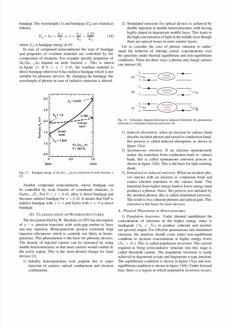
where E g is bandgap energy in eV.
In case of compound semiconductor the type of bandgap
and properties of resultant materials are controlled by the
composition of elements. For example specific properties of AlxGa1−xAs depend on mole fraction x. This is shown
in figure 11. If 0 < x < 0.45, the resultant material is
direct bandgap otherwise it has indirect bandgap which is not
suitable for photonic devices. By changing the bandgap, the
wavelength of photon in case of radiative emission is altered.
Fig. 11. Bandgap energy of AlxGa1−xAs as a function of mole fraction x
[2]
Another compound semiconductor, whose bandgap can
be controlled by mole fraction of constituent elements, is
GaAs1−xPx. For 0 < x < 0.45, alloy is direct bandgap and
becomes indirect bandgap for x > 0.45. It means that GaP is
indirect bandgap with x = 1 and GaAs with x = 0 is direct
bandgap.
III. CLASSIFICATION OF H ETEROSTRUCTURES
The first patent filed by W. Shockley in 1951 has description
of p − n junction transistor with wide-gap emitter to have
one-way injection. Heterojunctions possess extremely highinjection efficiencies which is certainly not likely in homo-
junctions. This phenomenon is the basis for photonic devices.
The density of injected carriers can be increased by using
double heterostructures so that more carriers would confine in
the active region. This is the most desired change for laser
devices [1].
1) Initially, heterojunctions were popular due to super
injection of carriers, optical confinement and electron
confinement.
2) Stimulated emission for optical devices is achieved by
double injection in double heterostructures with having
highly doped or degenerate middle layer. This leads to
the high concentration of light in the middle layer though
there are optical losses in outer emitter layers.
Let us consider the case of photon emission to under-
stand the behavior of altering carrier concentrations over
the junctions under thermal equilibrium and non-equilibriumconditions. There are three ways a photon and charge carriers
can interact [4].
Fig. 12. Schematic diagram showing (a) induced absorption (b) spontaneousemission (c) stimulated emission processes [4]
1) Induced absorption: when an electron in valence band
absorbs incident photon and raised to conduction band,
this process is called induced absorption, as shown in
figure 12(a).
2) Spontaneous emission: If an electron spontaneously
makes the transition from conduction band to valence
band, this is called spontaneous emission process as
shown in figure 12(b). This is the basis for light emitting
diode.
3) Stimulated or induced emission: When an incident pho-ton interact with an electron in conduction band and
causes electron transition to the valence band. This
transition from higher energy band to lower energy band
produces a photon. Since, this process was initiated by
the incident photon, this is called stimulated emission.
The result is two coherent photons and optical gain. This
emission is the basis for laser devices.
A. Physical Phenomena in Heterostructures
1) Population Inversion: Under thermal equilibrium the
concentration of electrons in the higher energy states is
inadequate (N 2 < N 1) to produce coherent and incoher-
ent spectral output. For efficient spontaneous and stimulatedemission, the junction should come under non-equilibrium
condition to increase concentration at higher energy levels
(N 2 > N 1). This is called population inversion. The current
required to bring semiconductor structure into this stage is
called threshold current. The population inversion is easily
achieved in degenerate p-type and degenerate n-type junction.
The equilibrium condition is shown in figure 13(a) and non-
equilibrium condition is shown in figure 13(b). Under forward
bias, there is a region in which population inversion occurs.
8/11/2019 Hetero Structures
http://slidepdf.com/reader/full/hetero-structures 7/11
In p-type region at the junction Fermi level E Fn is below the
conduction band, that region becomes more n-type. Similarly,
there is a region in n-type semiconductor near junction which
becomes more p-type. This population inversion is required
for lasing operation.
Fig. 13. Degenerated doped pn-junction (a) thermal equilibrium (b) forwardbias
The population inversion can be achieved by degenerating
the semiconductor. Also, there are heterojunctions where dou-
ble injection solves the population inversion problem without
using degenerate semiconductors.
2) Re-absorption: The re-absorption is the problem in
homojunction, the direct bandgap materials. The re-absorption
would happen when photon energy hν is greater than thebandgap energy. For such photons, the absorption coefficient is
not zero. This problem is fixed by using double heterojunctions
in which narrow bandgap material is surrounded by wider
bandgap materials as cladding layers. In this case, most of
the photons have energy less than the bandgap of materials
forming cladding layers. Thus, the absorption coefficient is
close to zero.
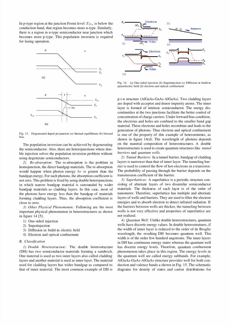
3) Other Physical Phenomenon: Following are the most
important physical phenomenon in heterostructures as shown
in figure 14 [5].
1) One-sided injection
2) Superinjection
3) Diffusion in build-in electric field
4) Electron and optical confinement
B. Classification
1) Double Heterostructure: The double heterostructure
(DH) has two semiconductor materials forming a sandwich.
One material is used as two outer layers also called cladding
layers and another material is used as inner layer. The material
used for cladding layers has wider bandgap as compared to
that of inner material. The most common example of DH is
Fig. 14. (a) One-sided injection (b) Superinjection (c) Diffusion in build-inquasielectric field (d) electron and optical confinement
p-i-n structure (AlGaAs-GaAs-AlGaAs). Two cladding layers
are doped with acceptor and donor impurity atoms. The inner
layer is formed of intrinsic semiconductor. The energy dis-
continuities at the two junctions facilitate the better control of concentration of charge carriers. Under forward bias condition,
the electrons and holes are confined to the smaller band gap
material. These electrons and holes recombine and leads to the
generation of photons. Thus electron and optical confinement
is one of the property of this example of heterostruture, as
shown in figure 14(d). The wavelength of photons depends
on the material composition of heterostructures. A double
heterostructure is used to create quantum structures like tunnel
barriers and quantum wells.
2) Tunnel Barriers: In a tunnel barrier, bandgap of cladding
layers is narrower than that of inner layer. The tunneling bar-
rier is used to control the flow of hot-electrons in a transistor.
The probability of passing through the barrier depends on thetransmission coefficient of the barrier.
3) Superlattices: A superlattice is a periodic structure con-
sisting of alternate layers of two dissimilar semiconductor
materials. The thickness of each layer is of the order of
nanometer. Therefore, superlattice has multiple and alternate
layers of wells and barriers. They are used to filter the electron
energies and to absorb electron to detect infrared radiation. If
the barriers between wells are thicker, the tunneling between
wells is not very effective and properties of superlattice are
not realized.
4) Quantum Well: Unlike double heterostructures, quantum
wells have discrete energy values. In double heterostrutures, if
the width of inner layer is reduced to the order of de Brogliewavelength, the resulting DH becomes quantum well. This
width is of the order few hundred angstroms. The inner layers
in DH has continuous energy states whereas the quantum well
has discrete energy levels. Therefore, quantum confinement
phenomenon takes place in this region. The energy levels in
the quantum well are called energy subbands. For example,
AlGaAs-GaAs-AlGaAs structure provides well for both con-
duction and valence bands a shown in Fig. 15. The schematic
diagrams for density of states and carrier distributions for
8/11/2019 Hetero Structures
http://slidepdf.com/reader/full/hetero-structures 8/11
quantum well and bulk materials are shown in figure 16.
Fig. 15. Quantum Well
Fig. 16. Schematic drawing of density of states function for bulk, quantumwell, quantum wire and quantum dot structures (black lines) and occupiedelectron states under excitation (red lines) [from ”Y. Arakawa and H. Sakaki
/ Appl. Phys. Lett. 40(11), 1982”]
5) Quantum Wire: If quantum confinement takes place in a
electrical conducting wire, it becomes a quantum wire. So, fur-
ther lowering the dimensions of quantum well heterostructures
results in quantum wire and quantum dot. In quantum wire,
the electrons move in discrete quantized energy states when
quantum wire is conducting. The conductance of quantum wire
is quantized in multiples of 2e2
h , where h is Planck’s constant
and e is electron charge. The conventional Ohm’s law does
not work.
6) Quantum Dots: The quantum dot is small enough that its
excitons are confined in all the three spatial directions. Theseare nanocrystals. In quantum dots, the size and bandgap are
inversely related. The emission frequencies increases as the
size of quantum dots decreases. Thus by changing the size of
quantum dots the color of emission changes.
Heterostructures are impacted by the reduction in dimen-
sional of semiconductor. The most important property is
density of states, which is shown in figure 17, with respect to
the dimension reduced from single heterostructure to double
heterostructure, quantum wire and finally quantum dots [5].
Fig. 17. Impact of dimension on the density of states
IV. DEVICES WITH H ETEROSTRUCTURE
A. Solar Cells
When light incident upon a semiconductor material, it
comes under non-equilibrium condition. The electrons from
valence band absorb photons and jump into conduction band.
This results in generation of electron-hole pairs. This is called
photovoltaic effect. The semiconductor structure possesses
build-in potential and photo current (I L) flows through it. As
a result, optical energy is converted into electrical energy. So,
the solar cell is a reversed-biased p-n junction with a resistive
load. The voltage drop across the resistive load tries to bring
p-n junction into forward bias with current (I F ) [4]. The net
current flows through in reverse-bias direction is given by the
following expression,
I = I L − I F = I L − I S
exp
eV
kT
− 1
(15)
The conversion efficiency of a solar cell is given by the
following expression
η = P m
P in× 100% =
I mV m
P in× 100% (16)
where P in is incident optical power and P m is maximum
solar power at current I m and voltage V m. The conversion
efficiency depends on the energy bandgap E g and other
non-ideal effects such as series resistance and reflection of
light from semiconductor material. The conversion efficiency
decreases with lattice temperature. The variation of conversion
efficiency with varying energy bandgap and temperature under
fixed recombination current is shown in figure 18.
B. Lasers
Lasers are sources of coherent light generated by recombi-
nation of electrons and holes using stimulated photon emission
process. The wavelength of light depends on the bandgap of
semiconductor material. The region of recombination is called
active region of lasers. This active region should be formed
of direct semiconductors. Other regions, also called cladding
layers, can be formed of indirect semiconductors. If cladding
8/11/2019 Hetero Structures
http://slidepdf.com/reader/full/hetero-structures 9/11
Fig. 18. Conversion efficienty of solar cell vs. bandgap with varyingtemperature
layers are of different materials, the structure is called double
heterostructures.
When current is below threshold value, the semiconductor
structure produces incoherent light through spontaneous emis-
sion and stimulated emission to produce coherent light starts
after threshold current. The threshold current for transition
from spontaneous to stimulated emission is shown in the figure
19. The electron confinement and optical confinement are the
most desired properties of a laser device and achieved by using
double heterostructure.
Fig. 19. Light vs. current relationship
The band diagram, index of refraction and intensity of
light with respect to the distance are shown in figure (20)
for a heterostructure laser. The advantages of using double
heterostructure in laser devices over single heterostructure and
homojunction laser devices are detailed out in figure 21. The
change in the refractive index from p-GaAs to p-AlxGa1−xAs
is 5% while for GaAs PN-homojunction is merely 1%. The
confinement of light is better in double heterostructure as
compared to other device configuration [6].
Fig. 20. Forward biased heterostructure (a) band diagram (b) referectiveindex (c) light intensity with respect to distance
Fig. 21. Comparision of band diagram under forward bias, refractive indexand intensity of light for (a) homojunction (b) single-heterostructure (c)double-heterostructure lasers. [Panish, Hayashi and Sumski, Ref. 48]
1) Buried Heterostructure Lasers: In practical semiconduc-
tor lasers, to achieve excellent carrier and optical confinement
the active region is buried inside a higher bandgap and lower
index material. This is called buried heterostructure (BH) laser
as shown in figure (22) [7]. The configurations in figure 22(b)
and (c) with semi-insulating (SI) regrowth are SI-BH lasers.
Because of low carrier concentrations the SI semiconductor
materials have high resistivity and due to large depletion of
carriers they have small capacitance. It is well known that

8/11/2019 Hetero Structures
http://slidepdf.com/reader/full/hetero-structures 10/11
devices with small parasitic capacitance are high speed devices
[7].
Fig. 22. Schematic cross sections of heterostructure with buried active layer(a) oxide (b) p-n reversed (c) semi-insulating (SI) stripe structures.
C. Light Emitting Diodes
A forward biased p-n junction produces spectral output due
to recombination of injected charge carriers at the metallur-
gical junction. This effect is called injection electrolumines-
cence. Such devices are Light Emitting Diode (LED). LEDs
with ordinary homojunction suffer from the following common
problems,
1) At the junction, high concentration of electrons and
holes are not achievable due to diffusion in the bulk
regions.
2) The concentration of electrons and holes is controlled
by the potential barriers which is same for both chargecarriers. These barriers are a function of only material
doping.
3) The emitted photons can be reabsorbed. Due to nonzero
absorption coefficient, efficiency of emitted light is re-
duced.
4) The high carrier concentration is achieved by employing
higher doping concentrations. This intern will increase
the probability of absorption.
But, in heterojunctions the potential barriers for electrons and
holes are different at the interface due to doping and difference
in energy bandgap of two different materials. To increase
the electron confinement, LED with double heterostructures
with wide-bandgap cladding layers is the choice. The spectralefficiency of a LED increases due to higher electron confine-
ment and optical confinement [8]. The difference in the carrier
concentrations for homojunction and double heterojunction is
shown in the figure 23. The double heterostructure forms a
quantum well therefore recombination rate is increased.
Under electric field, the charge carriers in quantum well
shift and, thus, emission is impacted with a shift called
”red-shift”. This effect can be reduced by decreasing the
size of quantum well thickness. Since, number of discrete
energy states in quantum well are limited due to quantum
confinement, saturation in the optical power occurs. The easier
solution is to increase the thickness of quantum well, But,
this would raise ”red-shift” effect. The efficient solution to
overcome this problem in a highly efficient LED is to use
multiple quantum wells. Figure 24(a) and 24(b) shows band
diagram of LED with quantum well and multiple quantum
wells. Therefore, a heterostructure LED is brighter than a
homojunction LED.
Fig. 23. Carrier concetrations under forward bias (a) homojunction (b) doubleheterostructure
Fig. 24. Schematic diagram for (a) quantum well LED (b) multiple quantumwell LED
D. Heterojunction Bipolar Transistor
The heterojunction bipolar transistor (HBT) has wide-gap
emitter. This results in higher value of current gain β (= I CI B
) as
compared to bipolar transistor with homojunctions [9]. Figureshows various currents in HBT as described below
1) I n, due to electrons injected from emitter into the base
2) I p, due to holes injected from base into the emitter
3) I s, due to recombination in the forward biased emitter-
base junction
4) I r, due to recombination of electrons part of I nThe net current in the three regions are expressed in terms of
these four current components
I E = I n + I p + I s (17)

8/11/2019 Hetero Structures
http://slidepdf.com/reader/full/hetero-structures 11/11