here MAX9634 nanoPoer 4-Bp UCSP/SOT23 Precision Crrent ... · The MAX9634 fits in a tiny, 1mm x 1mm...
9
General Description The MAX9634 high-side current-sense amplifier offers precision accuracy specifications of V OS less than 250μV (max) and gain error less than 0.5% (max). Quiescent supply current is an ultra-low 1μA. The MAX9634 fits in a tiny, 1mm x 1mm UCSP™ package size or a 5-pin SOT23 package, making the part ideal for applications in notebook computers, cell phones, PDAs, and all battery- operated portable devices where accuracy, low quiescent current, and small size are critical. The MAX9634 features an input common-mode voltage range from 1.6V to 28V. These current-sense amplifiers have a voltage output and are offered in four gain ver- sions: 25V/V (MAX9634T), 50V/V (MAX9634F), 100V/V (MAX9634H), and 200V/V (MAX9634W). The four gain selections offer flexibility in the choice of the external current-sense resistor. The very low 250μV (max) input offset voltage allows small 25mV to 50mV full-scale V SENSE voltage for very low voltage drop at full-current measurement. The MAX9634 is offered in tiny 4-bump UCSP (1mm x 1mm x 0.6mm footprint) and 5-pin SOT23 packages specified for operation over the -40°C to +85°C extended temperature range. Applications ● Cell Phones ● PDAs ● Power-Management Systems ● Portable/Battery-Powered Systems ● Notebook Computers Benefits and Features ● Ultra-Low Supply Current of 1μA (max) ● Low 250μV (max) Input Offset Voltage ● Low < 0.5% (max) Gain Error ● Input Common Mode: +1.6V to +28V ● Voltage Output ● Four Gain Versions Available • 25V/V (MAX9634T) • 50V/V (MAX9634F) • 100V/V (MAX9634H) • 200V/V (MAX9634W) ● Tiny 1mm x 1mm x 0.6mm, 4-Bump UCSP or 5-Pin SOT23 Packages 19-5021; Rev 4; 7/19 UCSP is a trademark of Maxim Integrated Products, Inc. +Denotes a lead(Pb)-free/RoHS-compliant package. Note: All devices are specified over the -40°C to +85°C extended temperature range. PART PIN- PACKAGE GAIN (V/V) TOP MARK MAX9634TERS+ 4 UCSP 25 +ABX MAX9634FERS+ 4 UCSP 50 +ABY MAX9634HERS+ 4 UCSP 100 +ABZ MAX9634WERS+ 4 UCSP 200 +ACA MAX9634TEUK+ 5 SOT23 25 +AFHG MAX9634FEUK+ 5 SOT23 50 +AFHH MAX9634HEUK+ 5 SOT23 100 +AFHI MAX9634WEUK+ 5 SOT23 200 +AFHJ MAX9634T/F/H/W MAX9634T/F/H/W 5 4 1 3 2 RS+ RS- GND OUT GND SOT23 UCSP TOP VIEW (BUMPS ON BOTTOM) B1 B2 A1 GND RS+ OUT RS- A2 DRAWINGS NOT TO SCALE MAX9634 nanoPower, 4-Bump UCSP/SOT23, Precision Current-Sense Amplifier Pin Configurations Ordering Information EVALUATION KIT AVAILABLE Click here for production status of specific part numbers.
Transcript of here MAX9634 nanoPoer 4-Bp UCSP/SOT23 Precision Crrent ... · The MAX9634 fits in a tiny, 1mm x 1mm...

General DescriptionThe MAX9634 high-side current-sense amplifier offers precision accuracy specifications of VOS less than 250μV (max) and gain error less than 0.5% (max). Quiescent supply current is an ultra-low 1μA. The MAX9634 fits in a tiny, 1mm x 1mm UCSP™ package size or a 5-pin SOT23 package, making the part ideal for applications in notebook computers, cell phones, PDAs, and all battery-operated portable devices where accuracy, low quiescent current, and small size are critical.The MAX9634 features an input common-mode voltage range from 1.6V to 28V. These current-sense amplifiers have a voltage output and are offered in four gain ver-sions: 25V/V (MAX9634T), 50V/V (MAX9634F), 100V/V (MAX9634H), and 200V/V (MAX9634W).The four gain selections offer flexibility in the choice of the external current-sense resistor. The very low 250μV (max) input offset voltage allows small 25mV to 50mV full-scale VSENSE voltage for very low voltage drop at full-current measurement.The MAX9634 is offered in tiny 4-bump UCSP (1mm x 1mm x 0.6mm footprint) and 5-pin SOT23 packages specified for operation over the -40°C to +85°C extended temperature range.
Applications Cell Phones PDAs Power-Management Systems Portable/Battery-Powered Systems Notebook Computers
Benefits and Features Ultra-Low Supply Current of 1μA (max) Low 250μV (max) Input Offset Voltage Low < 0.5% (max) Gain Error Input Common Mode: +1.6V to +28V Voltage Output Four Gain Versions Available
• 25V/V (MAX9634T)• 50V/V (MAX9634F)• 100V/V (MAX9634H)• 200V/V (MAX9634W)
Tiny 1mm x 1mm x 0.6mm, 4-Bump UCSP or 5-Pin SOT23 Packages
19-5021; Rev 4; 7/19
UCSP is a trademark of Maxim Integrated Products, Inc.
+Denotes a lead(Pb)-free/RoHS-compliant package.Note: All devices are specified over the -40°C to +85°Cextended temperature range.
PART PIN-PACKAGE
GAIN(V/V)
TOPMARK
MAX9634TERS+ 4 UCSP 25 +ABXMAX9634FERS+ 4 UCSP 50 +ABYMAX9634HERS+ 4 UCSP 100 +ABZMAX9634WERS+ 4 UCSP 200 +ACAMAX9634TEUK+ 5 SOT23 25 +AFHGMAX9634FEUK+ 5 SOT23 50 +AFHHMAX9634HEUK+ 5 SOT23 100 +AFHIMAX9634WEUK+ 5 SOT23 200 +AFHJ
MAX9634T/F/H/WMAX9634T/F/H/W
5 4
1 32
RS+ RS-
GND OUTGND
SOT23
UCSP
TOP VIEW(BUMPS ON BOTTOM)
B1 B2
A1
GND
RS+
OUT
RS-A2
DRAWINGS NOT TO SCALE
MAX9634 nanoPower, 4-Bump UCSP/SOT23, Precision Current-Sense Amplifier
Pin Configurations
Ordering Information
EVALUATION KIT AVAILABLE
Click here for production status of specific part numbers.
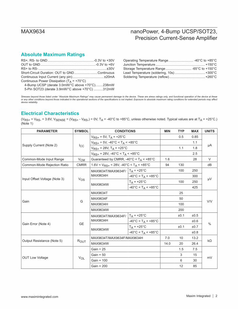
RS+, RS- to GND ..................................................-0.3V to +30VOUT to GND ............................................................-0.3V to +6VRS+ to RS- ..........................................................................±30VShort-Circuit Duration: OUT to GND .........................ContinuousContinuous Input Current (any pin) ..................................±20mAContinuous Power Dissipation (TA = +70°C)
4-Bump UCSP (derate 3.0mW/°C above +70°C) ........238mW 5-Pin SOT23 (derate 3.9mW/°C above +70°C) ..........312mW
Operating Temperature Range ........................... -40°C to +85°CJunction Temperature ......................................................+150°CStorage Temperature Range ............................ -65°C to +150°CLead Temperature (soldering, 10s) .................................+300°CSoldering Temperature (reflow) .......................................+260°C
(VRS+ = VRS- = 3.6V, VSENSE = (VRS+ - VRS-) = 0V, TA = -40°C to +85°C, unless otherwise noted. Typical values are at TA = +25°C.) (Note 1)
PARAMETER SYMBOL CONDITIONS MIN TYP MAX UNITS
Supply Current (Note 2) ICC
VRS+ = 5V, TA = +25°C 0.5 0.85
µAVRS+ = 5V, -40°C < TA < +85°C 1.1VRS+ = 28V, TA = +25°C 1.1 1.8VRS+ = 28V, -40°C < TA < +85°C 2.5
Common-Mode Input Range VCM Guaranteed by CMRR, -40°C < TA < +85°C 1.6 28 VCommon-Mode Rejection Ratio CMRR 1.6V < VRS+ < 28V, -40°C < TA < +85°C 94 130 dB
Input Offset Voltage (Note 3) VOS
MAX9634T/MAX9634F/MAX9634H
TA = +25°C 100 250
µV-40°C < TA < +85°C 300
MAX9634WTA = +25°C 100 250-40°C < TA < +85°C 425
Gain G
MAX9634T 25
V/VMAX9634F 50MAX9634H 100MAX9634W 200
Gain Error (Note 4) GE
MAX9634T/MAX9634F/MAX9634H
TA = +25°C ±0.1 ±0.5
%-40°C < TA < +85°C ±0.6
MAX9634WTA = +25°C ±0.1 ±0.7-40°C < TA < +85°C ±0.8
Output Resistance (Note 5) ROUTMAX9634T/MAX9634F/MAX9634H 7.0 10 13.2
kΩMAX9634W 14.0 20 26.4
OUT Low Voltage VOL
Gain = 25 1.5 7.5
mVGain = 50 3 15Gain = 100 6 30Gain = 200 12 85
MAX9634 nanoPower, 4-Bump UCSP/SOT23, Precision Current-Sense Amplifier
www.maximintegrated.com Maxim Integrated 2
Absolute Maximum Ratings
Stresses beyond those listed under “Absolute Maximum Ratings” may cause permanent damage to the device. These are stress ratings only, and functional operation of the device at these or any other conditions beyond those indicated in the operational sections of the specifications is not implied. Exposure to absolute maximum rating conditions for extended periods may affect device reliability.
Electrical Characteristics

(VRS+ = VRS- = 3.6V, VSENSE = (VRS+ - VRS-) = 0V, TA = -40°C to +85°C, unless otherwise noted. Typical values are at TA = +25°C.) (Note 1)
Note 1: All devices are 100% production tested at TA = +25°C. All temperature limits are guaranteed by design.Note 2: VOUT = 0. ICC is the total current into RS+ plus RS- pins.Note 3: VOS is extrapolated from measurements for the gain-error test.Note 4: Gain error is calculated by applying two values of VSENSE and calculating the error of the slope vs. the ideal:
Gain = 25, VSENSE is 20mV and 120mV. Gain = 50, VSENSE is 10mV and 60mV. Gain = 100, VSENSE is 5mV and 30mV. Gain = 200, VSENSE is 2.5mV and 15mV.
Note 5: The device is stable for any external capacitance value.Note 6: VOH is the voltage from VRS- to VOUT with VSENSE = 3.6V/gain.
(VRS+ = VRS- = 3.6V, TA = +25°C, unless otherwise noted.)
PARAMETER SYMBOL CONDITIONS MIN TYP MAX UNITSOUT High Voltage VOH VOH = VRS- - VOUT (Note 6) 0.1 0.2 V
Small-Signal Bandwidth(Note 5) BW
VSENSE = 50mV, gain = 25 125
kHzVSENSE = 50mV, gain = 50 60VSENSE = 50mV, gain = 100 30VSENSE = 50mV, gain = 200 15
Output Settling Time tS 1% final value, VSENSE = 50mV 100 µs
0
10
5
20
15
25
30
-0.4 -0.3 -0.2 -0.1 0 0.2 0.30.1 0.4
GAIN ERROR HISTOGRAM
MAX
9634
toc0
2
GAIN ERROR (%)
N (%
)
SUPPLY CURRENTvs. TEMPERATURE
MAX
9634
toc0
3
TEMPERATURE (°C)
SUPP
LY C
URRE
NT (µ
A)
10-15 35 60
0.4
0.2
0.6
0.8
1.0
1.2
1.4
28V
3.6V
1.8V
0-40 85
0
10
5
20
15
25
30
-0.4 -0.3 -0.2 -0.1 0 0.2 0.30.1 0.4
INPUT OFFSET VOLTAGE HISTOGRAM
MAX
9634
toc0
1
INPUT OFFSET VOLTAGE (mV)
N (%
)
MAX9634 nanoPower, 4-Bump UCSP/SOT23, Precision Current-Sense Amplifier
www.maximintegrated.com Maxim Integrated 3
Electrical Characteristics (continued)
Typical Operating Characteristics

(VRS+ = VRS- = 3.6V, TA = +25°C, unless otherwise noted.)
INPUT OFFSETvs. COMMON-MODE VOLTAGE
MAX
9634
toc0
4
COMMON-MODE VOLTAGE (V)
INPU
T OF
FSET
(µV)
2520105 15
-50
-45
-40
-35
-30
-550 30
INPUT OFFSETvs. TEMPERATURE
MAX
9634
toc0
5
INPU
T OF
FSET
(µV)
20
10
30
40
50
60
0
TEMPERATURE (°C)10-15 35 60-40 85
SUPPLY CURRENTvs. COMMON-MODE VOLTAGE
MAX
9634
toc0
6
COMMON-MODE VOLTAGE (V)
SUPP
LY C
URRE
NT (µ
A)
15 2010 305 25
1.0
0.8
0.6
0.4
0.2
1.2
1.4
00
-0.5
-0.3
-0.4
-0.1
-0.2
0
0.1
0 10 155 20 25 30
GAIN ERRORvs. COMMON-MODE VOLTAGE
MAX
9634
toc0
7
VOLTAGE (V)
GAIN
ERR
OR (%
)
GAIN ERRORvs. TEMPERATURE
MAX
9634
toc0
8
TEMPERATURE (°C)
GAIN
ERR
OR (%
)
10 60 8535-15
0.06
0.05
0.04
0.03
0.02
0.01
0.07
0.08
0-40
VOUT vs. VSENSE(SUPPLY = 3.6V)
MAX
9634
toc0
9
VSENSE (mV)
V OUT
(V)
10050
0.5
1.0
1.5
2.0
2.5
3.0
3.5
4.0
00 150
G = 100
G = 25
G = 50
VOUT vs. VSENSE(SUPPLY = 1.6V)
MAX
9634
toc1
0
VSENSE (mV)
V OUT
(V)
80604020
0.2
0.4
0.6
0.8
1.0
1.2
1.4
1.6
1.8
00 100
G = 100
G = 50
G = 25
SMALL-SIGNAL GAINvs. FREQUENCY
MAX
9634
toc1
1
FREQUENCY (Hz)
GAIN
(dB)
100k10 1M100 10k1k
-5
-10
-15
-20
-25
0
5
-301
AV = 25V/V
AV = 100V/V
AV = 50V/V
CMRRvs. FREQUENCY
MAX
9634
toc1
2
FREQUENCY (Hz)
CMRR
(dB)
100k10 1M100 10k1k
-40
-60
-80
-100
-120
-140
-20
0
-1601
G = 25
G = 50
G = 100
MAX9634 nanoPower, 4-Bump UCSP/SOT23, Precision Current-Sense Amplifier
Maxim Integrated 4www.maximintegrated.com
Typical Operating Characteristics (continued)
(VRS+ = VRS- = 3.6V, TA = +25°C, unless otherwise noted.)
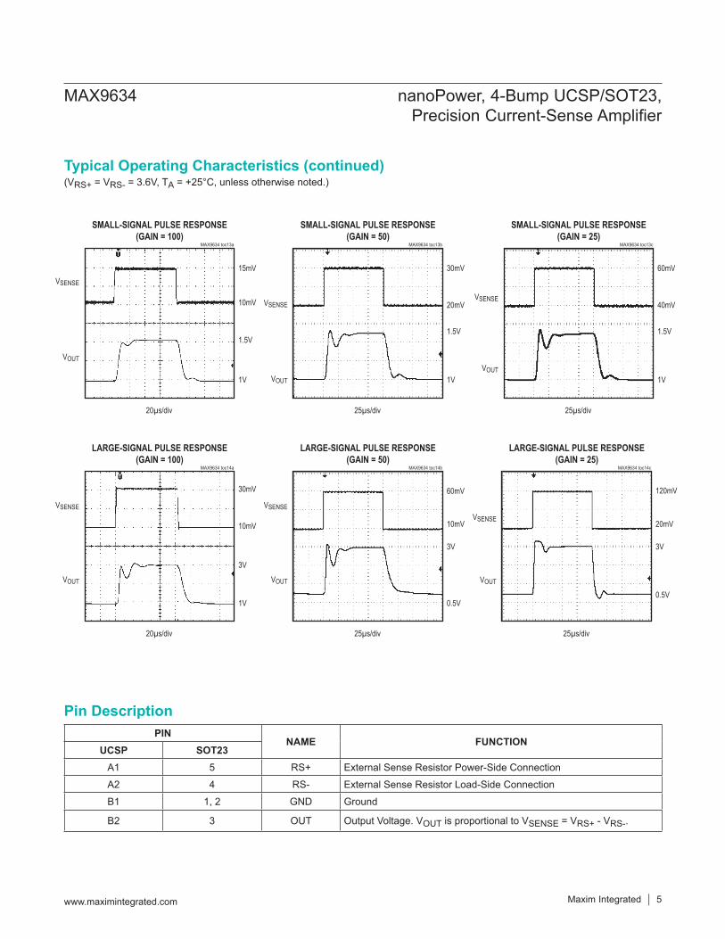
PINNAME FUNCTION
UCSP SOT23A1 5 RS+ External Sense Resistor Power-Side ConnectionA2 4 RS- External Sense Resistor Load-Side ConnectionB1 1, 2 GND Ground
B2 3 OUT Output Voltage. VOUT is proportional to VSENSE = VRS+ - VRS-.
SMALL-SIGNAL PULSE RESPONSE(GAIN = 100)
MAX9634 toc13a
20µs/div
VOUT
VSENSE
1V
1.5V
10mV
15mV
SMALL-SIGNAL PULSE RESPONSE(GAIN = 50)
MAX9634 toc13b
25µs/div
VOUT
VSENSE
1V
1.5V
20mV
30mV
SMALL-SIGNAL PULSE RESPONSE(GAIN = 25)
MAX9634 toc13c
25µs/div
VOUT
VSENSE
1V
1.5V
40mV
60mV
LARGE-SIGNAL PULSE RESPONSE(GAIN = 100)
MAX9634 toc14a
20µs/div
VOUT
VSENSE
1V
3V
10mV
30mV
LARGE-SIGNAL PULSE RESPONSE(GAIN = 50)
MAX9634 toc14b
25µs/div
VOUT
VSENSE
0.5V
3V
10mV
60mV
LARGE-SIGNAL PULSE RESPONSE(GAIN = 25)
MAX9634 toc14c
25µs/div
VOUT
VSENSE
0.5V
3V
20mV
120mV
MAX9634 nanoPower, 4-Bump UCSP/SOT23, Precision Current-Sense Amplifier
Maxim Integrated 5www.maximintegrated.com
Typical Operating Characteristics (continued)
Pin Description

Detailed DescriptionThe MAX9634 unidirectional high-side, current-sense amplifier features a 1.6V to 28V input common-mode range. This feature allows the monitoring of current out of a battery with a voltage as low as 1.6V. The MAX9634 monitors current through a current-sense resistor and amplifies the voltage across that resistor.The MAX9634 is a unidirectional current-sense amplifier that has a well-established history. An op amp is used to force the current through an internal gain resistor at RS+, which has a value of R1, such that its voltage drop equals the voltage drop across an external sense resis-tor, RSENSE. There is an internal resistor at RS- with the
same value as R1 to minimize offset voltage. The current through R1 is sourced by a high-voltage p-channel FET. Its source current is the same as its drain current, which flows through a second gain resistor, ROUT. This produc-es an output voltage, VOUT, whose magnitude is ILOAD x RSENSE x ROUT/R1. The gain accuracy is based on the matching of the two gain resistors R1 and ROUT (see Table 1). Total gain = 25V/V for the MAX9634T, 50V/V for the MAX9634F, 100V/V for the MAX9634H, and 200V/V for the MAX9634W. The output is protected from input overdrive by use of an output current-limiting circuit of 7mA (typical) and a 6V clamp protection circuit.
Applications InformationChoosing the Sense ResistorChoose RSENSE based on the following criteria:
Voltage LossA high RSENSE value causes the power-source voltage to drop due to IR loss. For minimal voltage loss, use the lowest RSENSE value.
Table 1. Internal Gain-Setting Resistors (Typical Values)
GAIN(V/V)
R1(Ω)
ROUT(kΩ)
200 100 20100 100 1050 200 1025 400 10
VBATT = 1.6V TO 28V
RSENSE
R1
ILOAD
ROUT
R1
GND
OUT
P
MAX9634
RS+ RS-
ADC
LOAD
µC
VDD = 3.3V
10kΩ
MAX9634 nanoPower, 4-Bump UCSP/SOT23, Precision Current-Sense Amplifier
www.maximintegrated.com Maxim Integrated 6
Typical Operating Circuit

OUT Swing vs. VRS+ and VSENSEThe MAX9634 is unique because the supply voltage is the input common-mode voltage (the average voltage at RS+ and RS-). There is no separate VCC supply voltage pin. Therefore, the OUT voltage swing is limited by the minimum voltage at RS+.
VOUT (max) = VRS+ (min) - VSENSE (max) - VOHand:
OUTSENSE
LOAD
V (max)RG I (max)
=×
VSENSE full scale should be less than VOUT/GAIN at the minimum RS+ voltage. For best performance with a 3.6V supply voltage, select RSENSE to provide approximately 120mV (gain of 25V/V), 60mV (gain of 50V/V), 30mV (gain of 100V/V), or 15mV (gain of 200V/V) of sense voltage for the full-scale current in each application. These can be increased by use of a higher minimum input voltage.
AccuracyIn the linear region (VOUT < VOUT (max)), there are two components to accuracy: input offset voltage (VOS) and gain error (GE). For the MAX9634, VOS = 250μV (max) and gain error is 0.5% (max). Use the linear equation:
VOUT = (gain ± GE) x VSENSE ± (gain x VOS)to calculate total error. A high RSENSE value allows lower currents to be measured more accurately because offsets are less significant when the sense voltage is larger.
Efficiency and Power DissipationAt high current levels, the I2R losses in RSENSE can be significant. Take this into consideration when choosing the resistor value and its power dissipation (wattage) rating. Also, the sense resistor’s value might drift if it is allowed to heat up excessively. The precision VOS of the MAX9634 allows the use of small sense resistors to reduce power dissipation and reduce hot spots.
Kelvin ConnectionsBecause of the high currents that flow through RSENSE, take care to eliminate parasitic trace resistance from causing errors in the sense voltage. Either use a four-terminal current-sense resistor or use Kelvin (force and sense) PCB layout techniques.
Optional Output Filter CapacitorWhen designing a system that uses a sample-and-hold stage in the ADC, the sampling capacitor momentarily loads OUT and causes a drop in the output voltage. If sampling time is very short (less than a microsecond), consider using a ceramic capacitor across OUT and GND to hold VOUT constant during sampling. This also decreases the small-signal bandwidth of the current-sense amplifier and reduces noise at OUT.
MAX9634 nanoPower, 4-Bump UCSP/SOT23, Precision Current-Sense Amplifier
www.maximintegrated.com Maxim Integrated 7
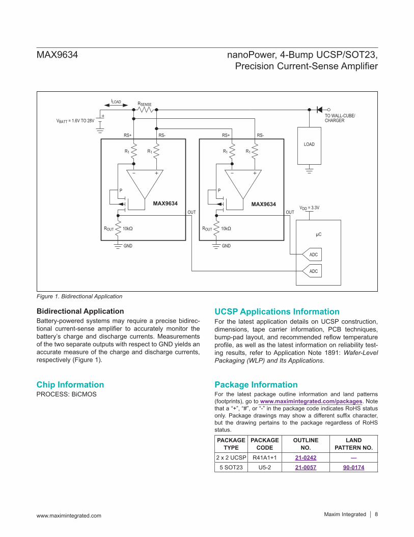
Bidirectional ApplicationBattery-powered systems may require a precise bidirec-tional current-sense amplifier to accurately monitor the battery’s charge and discharge currents. Measurements of the two separate outputs with respect to GND yields an accurate measure of the charge and discharge currents, respectively (Figure 1).
UCSP Applications InformationFor the latest application details on UCSP construction, dimensions, tape carrier information, PCB techniques, bump-pad layout, and recommended reflow temperature profile, as well as the latest information on reliability test-ing results, refer to Application Note 1891: Wafer-Level Packaging (WLP) and Its Applications.
Figure 1. Bidirectional Application
PACKAGE TYPE
PACKAGE CODE
OUTLINE NO.
LANDPATTERN NO.
2 x 2 UCSP R41A1+1 21-0242 —5 SOT23 U5-2 21-0057 90-0174
VBATT = 1.6V TO 28V
RSENSE
R1
ILOAD
ROUT
R1
GND
P
MAX9634
R1
ROUT
R1
GND
P
OUT OUT
TO WALL-CUBE/CHARGER
MAX9634
RS+ RS-RS- RS+
ADC
ADC
LOAD
µC
VDD = 3.3V
10kΩ10kΩ
MAX9634 nanoPower, 4-Bump UCSP/SOT23, Precision Current-Sense Amplifier
www.maximintegrated.com Maxim Integrated 8
Chip InformationPROCESS: BiCMOS
Package InformationFor the latest package outline information and land patterns (footprints), go to www.maximintegrated.com/packages. Note that a “+”, “#”, or “-” in the package code indicates RoHS status only. Package drawings may show a different suffix character, but the drawing pertains to the package regardless of RoHS status.

REVISIONNUMBER
REVISIONDATE DESCRIPTION PAGES
CHANGED0 10/09 Initial release —1 2/10 Corrected gain error limits in Electrical Characteristics table 22 8/10 Removed Power-Up Time parameter 33 3/17 Updated title to include “nanoPower” and updated package outline drawing 1–114 7/19 Updated TOC04 and TOC05 4
Maxim Integrated cannot assume responsibility for use of any circuitry other than circuitry entirely embodied in a Maxim Integrated product. No circuit patent licenses are implied. Maxim Integrated reserves the right to change the circuitry and specifications without notice at any time. The parametric values (min and max limits) shown in the Electrical Characteristics table are guaranteed. Other parametric values quoted in this data sheet are provided for guidance.
Maxim Integrated and the Maxim Integrated logo are trademarks of Maxim Integrated Products, Inc.
MAX9634 nanoPower, 4-Bump UCSP/SOT23, Precision Current-Sense Amplifier
© 2019 Maxim Integrated Products, Inc. 9
Revision History
For pricing, delivery, and ordering information, please visit Maxim Integrated’s online storefront at https://www.maximintegrated.com/en/storefront/storefront.html.