HD3SS6126 USB 3.0 Differential Switch 2:1/1:2 … USB 3.0 and USB 2.0 Differential Switch 2:1/1:2...
25
HD3SS6126 USB Connector USB Connector NoteBook Dock Station Connector USB HOST USB 2 Rx DP / DM USB 3 USB 3 Tx Product Folder Sample & Buy Technical Documents Tools & Software Support & Community HD3SS6126 SLAS975A – NOVEMBER 2013 – REVISED AUGUST 2015 HD3SS6126 USB 3.0 and USB 2.0 Differential Switch 2:1/1:2 MUX/DEMUX 1 Features 3 Description The HD3SS6126 device is a high-speed, passive 1• Ideal for USB Applications switch that is designed for USB applications to route – Signal Switch for USB 3.0 (SuperSpeed USB both SuperSpeed USB RX and TX and USB 2.0 DP and USB 2.0 HS/FS/LS) and DM signals from a source to two destinations or • Three Bidirectional Differential Pair Channel vice versa. The device can also be used for DisplayPort, PCI-Express™, SATA, SAS, and XAUI MUX/DEMUX Switches Also Suitable for applications. The HD3SS6126 device can be used in DisplayPort, PCIe Gen1/2/3, SATA 1.5/3/6G, SAS either sink-side or source-side applications. 1.5/3/6G and XAUI Applications • Supports Data Rates up to 10 Gbps on High- Device Information (1) Bandwidth Path (SS) PART NUMBER PACKAGE BODY SIZE (NOM) • V CC Operating Range 3.3 V ± 10% HD3SS6126 WQFN (42) 9.00 mm × 3.50 mm • Wide –3-dB Differential BW of More Than 10 GHz (1) For all available packages, see the orderable addendum at on High-Bandwidth Path (SS) the end of the data sheet. • Uses a Unique Adaptation Method to Maintain a Typical Application Diagram Constant Channel Impedance Over the Supported Common-Mode Voltage Range • Excellent High-bandwidth Path Dynamic Characteristics (at 2.5 GHz) – Crosstalk = –35 dB – Isolation = –23 dB – Insertion Loss = –1.1 dB – Return Loss = –11 dB • Small 3.5 mm × 9 mm, 42-Pin WQFN Package (RUA) • Active Mode Power = 8 mW 2 Applications • Desktop PCs • Notebook PCs • Tablets • Docking Stations • Telecommunications • Televisions 1 An IMPORTANT NOTICE at the end of this data sheet addresses availability, warranty, changes, use in safety-critical applications, intellectual property matters and other important disclaimers. PRODUCTION DATA.
-
Upload
nguyentruc -
Category
Documents
-
view
230 -
download
1
Transcript of HD3SS6126 USB 3.0 Differential Switch 2:1/1:2 … USB 3.0 and USB 2.0 Differential Switch 2:1/1:2...

HD
3SS
61
26
USB
Connector
USB
Connector
NoteBook
Dock Station
Connector
US
B H
OS
T
USB 2
Rx
DP / DM
USB 3
USB 3
Tx
Product
Folder
Sample &Buy
Technical
Documents
Tools &
Software
Support &Community
HD3SS6126SLAS975A –NOVEMBER 2013–REVISED AUGUST 2015
HD3SS6126 USB 3.0 and USB 2.0 Differential Switch 2:1/1:2 MUX/DEMUX1 Features 3 Description
The HD3SS6126 device is a high-speed, passive1• Ideal for USB Applications
switch that is designed for USB applications to route– Signal Switch for USB 3.0 (SuperSpeed USB both SuperSpeed USB RX and TX and USB 2.0 DPand USB 2.0 HS/FS/LS) and DM signals from a source to two destinations or
• Three Bidirectional Differential Pair Channel vice versa. The device can also be used forDisplayPort, PCI-Express™, SATA, SAS, and XAUIMUX/DEMUX Switches Also Suitable forapplications. The HD3SS6126 device can be used inDisplayPort, PCIe Gen1/2/3, SATA 1.5/3/6G, SASeither sink-side or source-side applications.1.5/3/6G and XAUI Applications
• Supports Data Rates up to 10 Gbps on High- Device Information(1)Bandwidth Path (SS)
PART NUMBER PACKAGE BODY SIZE (NOM)• VCC Operating Range 3.3 V ± 10% HD3SS6126 WQFN (42) 9.00 mm × 3.50 mm• Wide –3-dB Differential BW of More Than 10 GHz
(1) For all available packages, see the orderable addendum aton High-Bandwidth Path (SS) the end of the data sheet.• Uses a Unique Adaptation Method to Maintain a
Typical Application DiagramConstant Channel Impedance Over the SupportedCommon-Mode Voltage Range
• Excellent High-bandwidth Path DynamicCharacteristics (at 2.5 GHz)– Crosstalk = –35 dB– Isolation = –23 dB– Insertion Loss = –1.1 dB– Return Loss = –11 dB
• Small 3.5 mm × 9 mm, 42-Pin WQFN Package(RUA)
• Active Mode Power = 8 mW
2 Applications• Desktop PCs• Notebook PCs• Tablets• Docking Stations• Telecommunications• Televisions
1
An IMPORTANT NOTICE at the end of this data sheet addresses availability, warranty, changes, use in safety-critical applications,intellectual property matters and other important disclaimers. PRODUCTION DATA.

HD3SS6126SLAS975A –NOVEMBER 2013–REVISED AUGUST 2015 www.ti.com
Table of Contents7.2 Functional Block Diagram ....................................... 111 Features .................................................................. 17.3 Feature Description................................................. 112 Applications ........................................................... 17.4 Device Functional Modes........................................ 123 Description ............................................................. 1
8 Application and Implementation ........................ 134 Revision History..................................................... 28.1 Application Information............................................ 135 Pin Configuration and Functions ......................... 38.2 Typical Application ................................................. 136 Specifications......................................................... 5
9 Power Supply Recommendations ...................... 156.1 Absolute Maximum Ratings ...................................... 510 Layout................................................................... 156.2 ESD Ratings.............................................................. 5
10.1 Layout Guidelines ................................................. 156.3 Recommended Operating Conditions....................... 510.2 Layout Examples................................................... 156.4 Thermal Information .................................................. 6
11 Device and Documentation Support ................. 176.5 Electrical Characteristics – Device Parameters ........ 611.1 Community Resources.......................................... 176.6 Electrical Characteristics – Signal Switch
Parameters................................................................. 7 11.2 Trademarks ........................................................... 176.7 Switching Characteristics .......................................... 8 11.3 Electrostatic Discharge Caution............................ 176.8 Typical Characteristics ............................................ 10 11.4 Glossary ................................................................ 17
7 Detailed Description ............................................ 10 12 Mechanical, Packaging, and OrderableInformation ........................................................... 177.1 Overview ................................................................. 10
4 Revision HistoryNOTE: Page numbers for previous revisions may differ from page numbers in the current version.
Changes from Original (November 2013) to Revision A Page
• Added Pin Configuration and Functions section, ESD Ratings table, Typical Characteristics section, FeatureDescription section, Device Functional Modes, Application and Implementation section, Power SupplyRecommendations section, Layout section, Device and Documentation Support section, and Mechanical,Packaging, and Orderable Information section ..................................................................................................................... 1
2 Submit Documentation Feedback Copyright © 2013–2015, Texas Instruments Incorporated
Product Folder Links: HD3SS6126

NC
NC
NC
NC
NC
HS_OE
HSA(n)
SEL
HSA(p)
SSA0(p)
GND
SSA0(n)
VDD
NC
NC
NC
NC
HSC(n)
HSC(p)
HSB(n)
HSB(p)
VDD
SSB0(p)
SSB0(n)
SSB1(p)
SSB1(n)
SSC0(p)
SSC0(n)
SSC1(p)
SSC1(n)
GN
D
NC
VD
D
GN
D
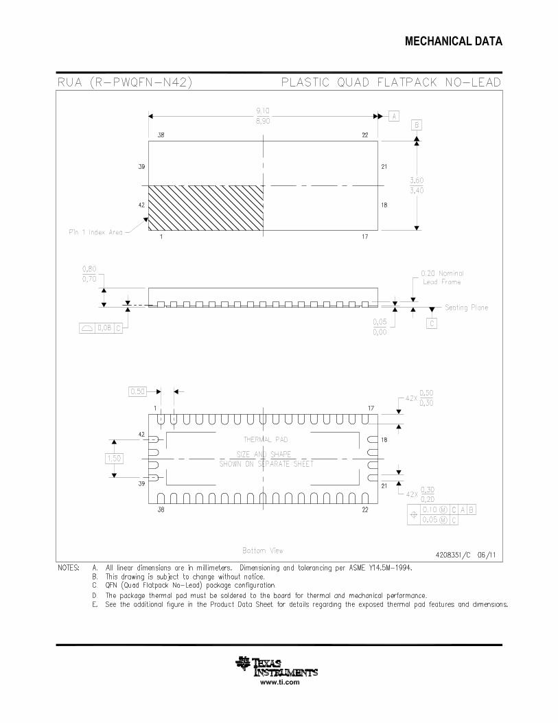
42
NC
41
NC
40
NC
20
NC
GND
GND
SSA1(p)
SSA1(n)
39
19
18
21
1
2
3
4
5
6
7
9
8
11
10
12
13
14
17
15
16
37
38
33
22
23
24
25
26
27
28
29
30
31
32
36
35
34
TQFN
HD3SS6126www.ti.com SLAS975A –NOVEMBER 2013–REVISED AUGUST 2015
5 Pin Configuration and Functions
RUA Package42-Pin WQFN
Top View
Copyright © 2013–2015, Texas Instruments Incorporated Submit Documentation Feedback 3
Product Folder Links: HD3SS6126

HD3SS6126SLAS975A –NOVEMBER 2013–REVISED AUGUST 2015 www.ti.com
Pin FunctionsPIN
I/O DESCRIPTIONNAME NO.
10, 14, 17,GND Supply Ground19, 21HSA(p) 8 Port A USB 2.0 positive signal
I/OHSA(n) 7 Port A USB 2.0 negative signalHSB(p) 31 Port B USB 2.0 positive signal
I/OHSB(n) 32 Port B USB 2.0 negative signalHSC(p) 33 Port C USB 2.0 positive signal
I/OHSC(n) 34 Port C USB 2.0 negative signal
Output EnableHS_OE 6 I (Control) H = Power Down
L = Normal Operation1, 2, 3, 4, 5,18, 35, 36,NC — Electrically No Connection37, 38, 39,40, 41, 42
SEL 9 I (Control) USB 3.0/2.0 Port Selection Control PinsSSA0(p) 11 Port A, Channel 0, USB 3.0 Positive Signal
I/OSSA0(n) 12 Port A, Channel 0, USB 3.0 Negative SignalSSA1(p) 15 Port A, Channel 1, USB 3.0 Positive Signal
I/OSSA1(n) 16 Port A, Channel 1, USB 3.0 Negative SignalSSB0(p) 29 Port B, Channel 0, USB 3.0 Positive Signal
I/OSSB0(n) 28 Port B, Channel 0, USB 3.0 Negative SignalSSB1(p) 27 Port B, Channel 1, USB 3.0 Positive Signal
I/OSSB1(n) 26 Port B, Channel 1, USB 3.0 Negative SignalSSC0(p) 25 Port C, Channel 0, USB 3.0 Positive Signal
I/OSSC0(n) 24 Port C, Channel 0, USB 3.0 Negative SignalSSC1(p) 23 Port C, Channel 1, USB 3.0 Positive Signal
I/OSSC1(n) 22 Port C, Channel 1, USB 3.0 Negative SignalVDD 13, 20, 30 Supply 3.3-V power supply voltage
4 Submit Documentation Feedback Copyright © 2013–2015, Texas Instruments Incorporated
Product Folder Links: HD3SS6126

HD3SS6126www.ti.com SLAS975A –NOVEMBER 2013–REVISED AUGUST 2015
6 Specifications
6.1 Absolute Maximum Ratingsover operating free-air temperature range (unless otherwise noted) (1)
MIN MAX UNITSupply Voltage, VDD
(2) –0.3 4 VDifferential I/O, High-bandwidth signal path: SSA0/1(p/n), SSB0/1(p/n), SSC0/1(p/n) –0.5 4
Voltage Differential I/O, Low-bandwidth signal path: HSAp/n), HSB(p/n), HSC(p/n) -0.5 7 VControl pin and single ended I/O –0.3 VDD + 0.3
Continuous power dissipation See Thermal InformationStorage temperature, Tstg –65 150 °C
(1) Stresses beyond those listed under Absolute Maximum Ratings may cause permanent damage to the device. These are stress ratingsonly and functional operation of the device at these or any conditions beyond those indicated under Recommended OperatingConditions is not implied. Exposure to absolute-maximum-rated conditions for extended periods may affect device reliability.
(2) All voltage values, except differential voltages, are with respect to network ground terminal.
6.2 ESD RatingsVALUE UNIT
Human body model (HBM), per ANSI/ESDA/JEDEC JS-001 (1) ±2000V(ESD) Electrostatic discharge VCharged device model (CDM), per JEDEC specification JESD22- ±500C101 (2)
(1) JEDEC document JEP155 states that 500-V HBM allows safe manufacturing with a standard ESD control process.(2) JEDEC document JEP157 states that 250-V CDM allows safe manufacturing with a standard ESD control process.
6.3 Recommended Operating Conditionstypical values for all parameters are at VCC = 3.3 V and TA = 25°C; all temperature limits are specified by design
MIN NOM MAX UNITVDD Supply voltage 3.0 3.3 3.6 VVIH Input high voltage Control Pins 2.0 VDD VVIL Input low voltage Control Pins –0.1 0.8 V
Switch I/O differential voltage for High-bandwidth signalVI/O_Diff Differential voltage 0 1.8 Vp-ppath only: SSA0/1(p/n), SSB0/1(p/n), SSC0/1(p/n)Switch I/O common mode voltage for High-bandwidth signalVI/O_CM Common voltage 0 2.0 Vpath only: SSA0/1(p/n), SSB0/1(p/n), SSC0/1(p/n)
TA Operating free-air temperature 0 70 °C
Copyright © 2013–2015, Texas Instruments Incorporated Submit Documentation Feedback 5
Product Folder Links: HD3SS6126

HD3SS6126SLAS975A –NOVEMBER 2013–REVISED AUGUST 2015 www.ti.com
6.4 Thermal InformationHD3SS6126
THERMAL METRIC RUA (WQFN) UNIT42 PINS
RθJA Junction-to-ambient thermal resistance 53.8 °C/WRθJC(top) Junction-to-case (top) thermal resistance 38.2 °C/WRθJB Junction-to-board thermal resistance 27.4 °C/WψJT Junction-to-top characterization parameter (1) 5.6 °C/WψJB Junction-to-board characterization parameter (1) 27.3 °C/W
(1) For more information about traditional and new thermal metrics, see Semiconductor and IC Package Thermal Metrics application report,SPRA953. Test conditions for ΨJB and ΨJT are clarified in the application report..
6.5 Electrical Characteristics – Device Parametersover recommended operating conditions (unless otherwise noted)
PARAMETER TEST CONDITIONS MIN TYP MAX UNITICC Supply current VDD = 3.6 V, SEL = VDD /GND; OE = GND; Outputs Floating 2.4 3 mASELIIH Input high current VDD = 3.6 V, VIN = VDD 95 µAIIL Input high current VDD = 3.6 V, VIN = GND 1 µAHS_OEIIH Input high current VDD = 3.6 V, VIN = VDD 1 µAIIL Input high current VDD = 3.6 V, VIN = GND 1 µASSA0/1, SSB0/1, SSC0/1
VDD = 3.6 V, VIN = 2 V, VOUT= 2 V, 130(ILK on open outputs Port B and C)High-impedance leakageILK µAcurrent VDD = 3.6 V, VIN = 2 V, VOUT= 2 V, 4(ILK on open outputs Port A)HSA, HSB, HSC
High-impedance leakage VDD = 3.6 V, VIN = 0 V, VOUT= 0 V to 4 V,ILK 1 µAcurrent HS_OE_IN = GND
6 Submit Documentation Feedback Copyright © 2013–2015, Texas Instruments Incorporated
Product Folder Links: HD3SS6126

HD3SS6126www.ti.com SLAS975A –NOVEMBER 2013–REVISED AUGUST 2015
6.6 Electrical Characteristics – Signal Switch Parametersunder recommended operating conditions; RL, RSC = 50 Ω, CL = 10 pF (unless otherwise noted)
PARAMETER TEST CONDITIONS MIN TYP MAX UNITSSA0/1(p/n), SSB0/1(p/n), SSC0/1(p/n) Signal PathCON Outputs ON capacitance VIN = 0 V, outputs open, switch ON 1.5 pFCOFF Outputs OFF capacitance VIN = 0 V, outputs open, switch OFF 1 pF
VDD = 3.3 V, VCM = 0 V – 2 V,RON Output ON resistance 5 8 ΩIO = –8 mAVDD = 3.3 V; 0 V ≤ VIN ≤ 2 V;ON resistance match between pairsΔRON 0.7 Ωof the same channel IO = –8 mA
ON resistance flatnessRFLAT_ON VDD = 3.3 V; –0 V ≤ VIN ≤ 2 V 1.15 Ω(RON(MAX)– RON(MIN)
f = 0.3 MHz –25Differential return lossRL f = 2.5 GHz –11 dB(VCM = 0 V)
f = 4 GHz –11f = 0.3 MHz -85
Differential crosstalkXTALK f = 2.5 GHz –35 dB(VCM = 0 V)f = 4 GHz –33f = 0.3 MHz -85
Differential off-isolationOIRR f = 2.5 GHz -23 dB(VCM = 0 V)f = 4 GHz –21f = 0.3 MHz –0.43
Differential insertion lossIL f = 2.5 GHz –1.1 dB(VCM = 0 V)f = 4 GHz –1.3
BW Bandwidth At –3 dB 10 GHzHSA(p/n), HSB(p/n), HSC(p/n) SIGNAL PATHCON Outputs ON capacitance VIN = 0 V, Outputs Open, Switch ON 6 7.5 pFCOFF Outputs OFF capacitance VIN = 0 V, Outputs Open, Switch OFF 3.5 6 pF
VDD = 3 V, VIN = 0 V, 3 6IO = 30 mARON Output ON resistance Ω
VDD = 3 V, VIN = 2.4 V, 3.4 6IO = 30 mAVDD = 3 V; VIN = 0 V; 0.2IO = 30 mAON resistance match between pairsΔRON Ωof the same channel VDD = 3 V; VIN = 1.7 V; 0.2IO = -15 mAVDD = 3 V; VIN = 0 V; 1IO = 30 mAON resistance flatnessRFLAT_ON Ω(RON(MAX)– RON(MIN ) VDD = 3 V; VIN = 1.7 V; 1IO = –15 mA
XTALK Differential crosstalk (VCM = 0 V) RL = 50 Ω, f = 250 MHz –40 dBOIRR Differential off-isolation (VCM = 0 V) RL = 50 Ω, f = 250 MHz –41 dBBW Bandwidth RL = 50 Ω 0.9 GHz
Copyright © 2013–2015, Texas Instruments Incorporated Submit Documentation Feedback 7
Product Folder Links: HD3SS6126

CL(2) RL
VIN
VCC
GND
HSB or HSC VOUT1 or VOUT2
VCTRL
HSB or HSC
HSA
Logic
Input (1)
V+
VCOM
500 Ω
RL CL
50 pFtON
TEST
V+500 Ω 50 pFtOFF
50%
tON tOFF
50%
90% 90%
Logic
Input
(VI)
1.8 V
Switch
Output
(VOUT1 or VOUT2)
0
CL(2) RL
SEL
(1)
(2) CL includes probe and jig capacitance.
VOH
VOL
All input pulses are supplied by generators have the following characteristics: PRR 10 , Z = 50 , t < 5 ns, tO Ω r f < 5 ns.≤ MHZ
VOUT
90%
10%
50%
ton
toff
SEL
HD3SS6126SLAS975A –NOVEMBER 2013–REVISED AUGUST 2015 www.ti.com
6.7 Switching Characteristicsover operating free-air temperature range (unless otherwise noted)
PARAMETER TEST CONDITIONS MIN TYP MAX UNITSSA0/1(p/n), SSB0/1(p/n), SSC0/1(p/n) Signal Pathton SEL-to-Switch ton RSC and RL = 50 Ω, See Figure 1 70 250 nstoff SEL-to-Switch toff RSC and RL = 50 Ω, See Figure 1 70 250 nstPD Switch propagation delay RSC and RL = 50 Ω, See Figure 3 85 pstSK(O) Interpair output skew (CH-CH) RSC and RL = 50 Ω, See Figure 3 20 pstSK(b-b) Intrapair Output Skew (bit-bit) RSC and RL = 50 Ω, See Figure 3 8 psHSA(p/n), HSB(p/n), HSC(p/n) SIGNAL PATH
SEL to Switch tON See Figure 2 30tON ns
HS_OE to Switch tON See Figure 2 17SEL to Switch tOFF See Figure 2 12
tOFF nsHS_OE to Switch tOFF See Figure 2 10
tPD(1) Switch propagation delay See Figure 3 250 ps
tSK(O)(1) Interpair output skew (CH-CH) 100 200 ps
tSK(P)(1) Intrapair Output Skew (bit-bit) 100 200 ps
(1) Specified by design
Figure 1. Select to Switch tON and tOFF
Figure 2. Turnon (tON) and Turnoff Time (tOFF)
8 Submit Documentation Feedback Copyright © 2013–2015, Texas Instruments Incorporated
Product Folder Links: HD3SS6126

50% 50%
50% 50%
tP1 tP2
tSK(O) = Difference between tPD for any
two pairs of outputs
tSK(b-b) = 0.5 X |(t4 – t3) + (t1 – t2)|
50 Ω
50 Ω
B/C(p)A(p)
50 Ω
50 Ω
B/C(n)A(n)
SEL
HD
3S
S6126
Vcc
C/B (p)
C/B (n)
50%
tSK(O)
tPD = Max(tp1, tp2)
t3 t4t1 t2
B/C(p)
B/C(n)
A(p)
A(n)
A (p)
A (n)
C/B/A (p)
C/B/A (n)
C/B/A (p)
C/B/A (n)
NOTES:
1. Measurements based on an ideal input with zero intrapair skew on
the input, i.e. the input at A to B/C or the input at B/C to A
2. Interpair skew is measured from lane to lane on the same channel,
e.g. C0 to C1
3. Intrapair skew is defined as the relative difference from the p and n
signals of a single lane
Intrapair skew
Interpair skew
HD3SS6126www.ti.com SLAS975A –NOVEMBER 2013–REVISED AUGUST 2015
Figure 3. Propagation Delay and Skew
Copyright © 2013–2015, Texas Instruments Incorporated Submit Documentation Feedback 9
Product Folder Links: HD3SS6126

Temperature (qC)
SK
EW
(ps
)
0 5 10 15 20 25 30 35 40 45 50 55 60 65 700.375
0.385
0.395
0.405
0.415
0.425
0.435
0.445
0.455
0.465
0.475
D001Temperature (qC)
SK
EW
(ps
)
0 5 10 15 20 25 30 35 40 45 50 55 60 65 700.575
0.58
0.585
0.59
0.595
0.6
0.605
0.61
0.615
0.62
0.625
D002
HD3SS6126SLAS975A –NOVEMBER 2013–REVISED AUGUST 2015 www.ti.com
6.8 Typical Characteristics
Figure 4. Intrapair Skew SSA to SSB Port Figure 5. Intrapair Skew SSA to SSC Port
7 Detailed Description
7.1 OverviewThe HD3SS6126 is a USB 3.0 and USB 2.0 differential switch, it is designed to support data rates up to 10 Gbpson high-bandwidth paths (SS), it is also suitable for DisplayPort, PCIe Gen1/2/3, SATA 1.5/3/6G, SAS 1.5/3/6Gand XAUI applications. The device uses a unique adaptation method to maintain a constant channel impedanceover the supported common-mode voltage range, resulting in an excellent high-bandwidth path dynamiccharacteristics (at 2.5 GHz; Crosstalk = –35 dB, Isolation = –23 dB, Insertion Loss = –1.1 dB, Return Loss = –11dB).
10 Submit Documentation Feedback Copyright © 2013–2015, Texas Instruments Incorporated
Product Folder Links: HD3SS6126

SSA1(n)
SSA1(p)
GND
GND
NC
NC
NC
NC
GN
D
VD
D
NC
GN
D
SSC1(n)
SSC1(p)
SSC0(n)
SSC0(p)
SSB1(n)
SSB1(p)
SSB0(n)
SSB0(p)
VDD
HSB(p)
HSB(n)
HSC(p)
HSC(n)
NC
NC
NC
NC
VDD
SSA0(n)
GND
SSA0(p)
HSA(p)
SEL
n)HSA(
HS_OE
NC
NC
NC
NC
1
2
3
4
5
6
7
9
8
11
10
12
13
42
41
40
20
14
17
15
16
34
35
36
37
38
32
31
30
29
28
27
26
25
24
23
22
33
39
19
18
21
NC
HD3SS6126www.ti.com SLAS975A –NOVEMBER 2013–REVISED AUGUST 2015
7.2 Functional Block Diagram
7.3 Feature DescriptionThe HD3SS6126 can be powered by VBUS from the USB Host, and is capable of selecting USB2 independentlyfrom USB3. Although the main application of the HD3SS6126 is USB3.0/2.0, the device also supports commoninterfaces such as PCIe Gen1 and Gen2, DP and SATA/SAS applications. The device is able to support theseadditional interfaces because of its support of data rates up to 5.4 Gbps and common-mode voltages from 0 V to2 V with a maximum signal swing of 1.8 V. All of these applications use an 8b or 10b coding technique toachieve DC balance and facilitate terminal equipment.
NOTEThe device may need AC capacitors and additional bias voltage to support the PCIe Gen1and Gen2 interfaces.
Copyright © 2013–2015, Texas Instruments Incorporated Submit Documentation Feedback 11
Product Folder Links: HD3SS6126

HD3SS6126SLAS975A –NOVEMBER 2013–REVISED AUGUST 2015 www.ti.com
7.4 Device Functional Modes
Table 1. Truth Table USB 3.0 SuperSpeed USB
USB 3.0 PORT SELECTIONSEL
SSA0/1 SSB0/1 SSC0/1
0 To/From SSB0/1 To/From SSA0/1 Off
1 To/From SSC0/1 Off To/From SSA0/1
Table 2. Truth Table USB 2.0 High-Speed, Full-Speed, Low-Speed PathUSB 2.0 Port Selection
HS_OE SELHSA HSB HSC
0 0 To/From HSB To/From HSA Off0 1 To/From HSC Off To/From HSA1 X Off Off Off
12 Submit Documentation Feedback Copyright © 2013–2015, Texas Instruments Incorporated
Product Folder Links: HD3SS6126

HD3SS6126x N
PCIe/DP/USB/SATA Signal Source
PCIe/DP/USB/SATA Signal Sink 2
PCIe/DP/USB/SATA Signal Sink 1
HD3SS6126x N
PCIe/DP/USB/SATA Signal Sink
PCIe/DP/USB/SATA Signal Source 2
PCIe/DP/USB/SATA Signal Source 1
HD3SS6126www.ti.com SLAS975A –NOVEMBER 2013–REVISED AUGUST 2015
8 Application and Implementation
NOTEInformation in the following applications sections is not part of the TI componentspecification, and TI does not warrant its accuracy or completeness. TI’s customers areresponsible for determining suitability of components for their purposes. Customers shouldvalidate and test their design implementation to confirm system functionality.
8.1 Application InformationA typical application for the HD3SS6126 is a USB 3.0 KVM switch, where one of two USB hosts system can beselected for an USB device. These guidelines are also suitable for PCIe(Gen1,Gen2), SATA, XAUI and DP,since the HD3SS6126 device is fully compatible with these protocols.
8.2 Typical Application
Figure 6. Two Signal Sources to One Destination
Figure 7. One Signal Sources to Two Destination
Copyright © 2013–2015, Texas Instruments Incorporated Submit Documentation Feedback 13
Product Folder Links: HD3SS6126

HD3SS6126SLAS975A –NOVEMBER 2013–REVISED AUGUST 2015 www.ti.com
Typical Application (continued)8.2.1 Design RequirementsPower supply requirements:• VDD from 3 V to 3.6 V
Control pins requirements• VIH from 2 V to VDD• VIL from –0.1 V to 0.8 V
Differential pairs requirements:• VI/O_Diff from 0 V to 1.8 Vp-p• VI/O_CM from 0 V to 2 V
TA Operating free-air temperature from 0°C to 70°C
8.2.2 Detailed Design Procedure
8.2.2.1 Power SupplyThe first step is to design the power supply and determine the VCC stability and minimum current required (seePower Supply Recommendations).
8.2.2.2 Differential PairsAll of the interfaces the HD3SS6126 device supports require AC coupling between the transmitter and receiver.TI recommends using 0402-sized capacitors to provide AC coupling, but 0603-sized capacitors are alsoacceptable. Both 0805-sized capacitors and C-packs should be avoided. Best practice is to place AC-couplingcapacitors symmetrically. A capacitor value of 0.1uF is best and the value should be matched for the +/-signalpair. The placement should be along the TX pairs on the system board, which are usually routed on the top layerof the board.
All differential pairs must have a matched impedance according to the implemented protocol: 100-Ω differential(±10%) for PCIe and 90-Ω differential (±15%) for USB 2.0 and USB 3.0.
The control logic can be implemented by use of an external control processor or by using a simple selectorswitch. TI recommends using 5-kΩ pullup and pulldown resistors on the control signals, if they are included. Thecontrol logic must not violate the input voltage parameters outlined in the Recommended Operating Conditionstable.
8.2.3 Application Curves
Figure 9. USB 3.0 TX Eye Pattern Test With 3-Inch 5-milFigure 8. USB 3.0 TX Eye Pattern Test With 3-Inch 5-milDifferential PCB Trace With HD3SS6126Differential PCB Trace Without HD3SS6126
14 Submit Documentation Feedback Copyright © 2013–2015, Texas Instruments Incorporated
Product Folder Links: HD3SS6126

Layer 1: High-Speed Diff-Signal Traces
Layer 2: GND Plane
Layer 3: Power Plane
Layer 4: Low-Speed Signal Traces
S
W
t+ -
h 0r
L
X
HD3SS6126www.ti.com SLAS975A –NOVEMBER 2013–REVISED AUGUST 2015
9 Power Supply RecommendationsThe power supply must provide a constant voltage with a 10% maximum variation of the nominal value, and hasto be able to provide at least 3 mA for the HD3SS6126 only (based on the maximum power consumption). It isalso possible to provide the power supply from VBUS from the Host, just by including a voltage regulatorpowered through VBUS. Each VCC pin must have a 0.1-µF bypass capacitor placed as closely as possible. TIrecommends including two extra capacitors in parallel, which should be also placed as closely as possible to theVCC pin. The suggested values for these extra capacitors are 1 µF and 0.01 µF.
10 Layout
10.1 Layout GuidelinesGenerally, impedance match becomes critical in such high-speed signal applications to avoid reflection. Eachdifferential-signal pair must have a differential impedance of about 90 Ω ±15% (for PCIe or DP, 100 Ω ±10%)with single-end signal impedance about 50 Ω to ground. Usually, Microstrip is used to accomplish impedancematch. Four layers are recommended for a low-EMI PCB design. shows physical geometries of differential tracesto form Microstrip. In order to better maintain signal integrity, reference the following:1. Route high-speed differential signals on the top layer with a solid ground layer under them to accomplish
controlled impedance, while avoiding vias and stubs which may cause impedance discontinuities. If viasmust be used, make sure the space of the vias is as minimal as possible.
2. Be sure both the length of differential traces and the length of differential signal pairs are matched in order toreduce intrapair skew and interpair skew separately which also does good to low EMI. TI recommendskeeping the space of the traces of the differential signal the same across the entire length of the trace tokeep impedance match and reduce EMI.
3. Route low-speed, but fast-edged control signals on the bottom layer to minimize the crosstalk of the high-speed signal.
4. For other adjacent signal traces on the same layer, make distance L ≥ 3 S to facilitate impedance match.5. TI reccommends using 45° bends instead of 90° bends in order to maintain signal integrity and low EMI.
10.2 Layout Examples
Figure 10. PCB Layers Example
Copyright © 2013–2015, Texas Instruments Incorporated Submit Documentation Feedback 15
Product Folder Links: HD3SS6126

HD3SS6126SLAS975A –NOVEMBER 2013–REVISED AUGUST 2015 www.ti.com
Layout Examples (continued)
Figure 11. USB Signals Routing Example
16 Submit Documentation Feedback Copyright © 2013–2015, Texas Instruments Incorporated
Product Folder Links: HD3SS6126

HD3SS6126www.ti.com SLAS975A –NOVEMBER 2013–REVISED AUGUST 2015
11 Device and Documentation Support
11.1 Community ResourcesThe following links connect to TI community resources. Linked contents are provided "AS IS" by the respectivecontributors. They do not constitute TI specifications and do not necessarily reflect TI's views; see TI's Terms ofUse.
TI E2E™ Online Community TI's Engineer-to-Engineer (E2E) Community. Created to foster collaborationamong engineers. At e2e.ti.com, you can ask questions, share knowledge, explore ideas and helpsolve problems with fellow engineers.
Design Support TI's Design Support Quickly find helpful E2E forums along with design support tools andcontact information for technical support.
11.2 TrademarksE2E is a trademark of Texas Instruments.PCI-Express is a trademark of PCI-SIG.All other trademarks are the property of their respective owners.
11.3 Electrostatic Discharge CautionThese devices have limited built-in ESD protection. The leads should be shorted together or the device placed in conductive foamduring storage or handling to prevent electrostatic damage to the MOS gates.
11.4 GlossarySLYZ022 — TI Glossary.
This glossary lists and explains terms, acronyms, and definitions.
12 Mechanical, Packaging, and Orderable InformationThe following pages include mechanical, packaging, and orderable information. This information is the mostcurrent data available for the designated devices. This data is subject to change without notice and revision ofthis document. For browser-based versions of this data sheet, refer to the left-hand navigation.
Copyright © 2013–2015, Texas Instruments Incorporated Submit Documentation Feedback 17
Product Folder Links: HD3SS6126

PACKAGE OPTION ADDENDUM
www.ti.com 19-Mar-2015
Addendum-Page 1
PACKAGING INFORMATION
Orderable Device Status(1)
Package Type PackageDrawing
Pins PackageQty
Eco Plan(2)
Lead/Ball Finish(6)
MSL Peak Temp(3)
Op Temp (°C) Device Marking(4/5)
Samples
HD3SS6126RUAR ACTIVE WQFN RUA 42 3000 Green (RoHS& no Sb/Br)
CU NIPDAU Level-3-260C-168 HR 0 to 70 HD3SS6126
(1) The marketing status values are defined as follows:ACTIVE: Product device recommended for new designs.LIFEBUY: TI has announced that the device will be discontinued, and a lifetime-buy period is in effect.NRND: Not recommended for new designs. Device is in production to support existing customers, but TI does not recommend using this part in a new design.PREVIEW: Device has been announced but is not in production. Samples may or may not be available.OBSOLETE: TI has discontinued the production of the device.
(2) Eco Plan - The planned eco-friendly classification: Pb-Free (RoHS), Pb-Free (RoHS Exempt), or Green (RoHS & no Sb/Br) - please check http://www.ti.com/productcontent for the latest availabilityinformation and additional product content details.TBD: The Pb-Free/Green conversion plan has not been defined.Pb-Free (RoHS): TI's terms "Lead-Free" or "Pb-Free" mean semiconductor products that are compatible with the current RoHS requirements for all 6 substances, including the requirement thatlead not exceed 0.1% by weight in homogeneous materials. Where designed to be soldered at high temperatures, TI Pb-Free products are suitable for use in specified lead-free processes.Pb-Free (RoHS Exempt): This component has a RoHS exemption for either 1) lead-based flip-chip solder bumps used between the die and package, or 2) lead-based die adhesive used betweenthe die and leadframe. The component is otherwise considered Pb-Free (RoHS compatible) as defined above.Green (RoHS & no Sb/Br): TI defines "Green" to mean Pb-Free (RoHS compatible), and free of Bromine (Br) and Antimony (Sb) based flame retardants (Br or Sb do not exceed 0.1% by weightin homogeneous material)
(3) MSL, Peak Temp. - The Moisture Sensitivity Level rating according to the JEDEC industry standard classifications, and peak solder temperature.
(4) There may be additional marking, which relates to the logo, the lot trace code information, or the environmental category on the device.
(5) Multiple Device Markings will be inside parentheses. Only one Device Marking contained in parentheses and separated by a "~" will appear on a device. If a line is indented then it is a continuationof the previous line and the two combined represent the entire Device Marking for that device.
(6) Lead/Ball Finish - Orderable Devices may have multiple material finish options. Finish options are separated by a vertical ruled line. Lead/Ball Finish values may wrap to two lines if the finishvalue exceeds the maximum column width.
Important Information and Disclaimer:The information provided on this page represents TI's knowledge and belief as of the date that it is provided. TI bases its knowledge and belief on informationprovided by third parties, and makes no representation or warranty as to the accuracy of such information. Efforts are underway to better integrate information from third parties. TI has taken andcontinues to take reasonable steps to provide representative and accurate information but may not have conducted destructive testing or chemical analysis on incoming materials and chemicals.TI and TI suppliers consider certain information to be proprietary, and thus CAS numbers and other limited information may not be available for release.
In no event shall TI's liability arising out of such information exceed the total purchase price of the TI part(s) at issue in this document sold by TI to Customer on an annual basis.

PACKAGE OPTION ADDENDUM
www.ti.com 19-Mar-2015
Addendum-Page 2

TAPE AND REEL INFORMATION
*All dimensions are nominal
Device PackageType
PackageDrawing
Pins SPQ ReelDiameter
(mm)
ReelWidth
W1 (mm)
A0(mm)
B0(mm)
K0(mm)
P1(mm)
W(mm)
Pin1Quadrant
HD3SS6126RUAR WQFN RUA 42 3000 330.0 16.4 3.8 9.3 1.0 8.0 16.0 Q1
PACKAGE MATERIALS INFORMATION
www.ti.com 19-Mar-2015
Pack Materials-Page 1

*All dimensions are nominal
Device Package Type Package Drawing Pins SPQ Length (mm) Width (mm) Height (mm)
HD3SS6126RUAR WQFN RUA 42 3000 367.0 367.0 38.0
PACKAGE MATERIALS INFORMATION
www.ti.com 19-Mar-2015
Pack Materials-Page 2
IMPORTANT NOTICE
Texas Instruments Incorporated and its subsidiaries (TI) reserve the right to make corrections, enhancements, improvements and otherchanges to its semiconductor products and services per JESD46, latest issue, and to discontinue any product or service per JESD48, latestissue. Buyers should obtain the latest relevant information before placing orders and should verify that such information is current andcomplete. All semiconductor products (also referred to herein as “components”) are sold subject to TI’s terms and conditions of salesupplied at the time of order acknowledgment.TI warrants performance of its components to the specifications applicable at the time of sale, in accordance with the warranty in TI’s termsand conditions of sale of semiconductor products. Testing and other quality control techniques are used to the extent TI deems necessaryto support this warranty. Except where mandated by applicable law, testing of all parameters of each component is not necessarilyperformed.TI assumes no liability for applications assistance or the design of Buyers’ products. Buyers are responsible for their products andapplications using TI components. To minimize the risks associated with Buyers’ products and applications, Buyers should provideadequate design and operating safeguards.TI does not warrant or represent that any license, either express or implied, is granted under any patent right, copyright, mask work right, orother intellectual property right relating to any combination, machine, or process in which TI components or services are used. Informationpublished by TI regarding third-party products or services does not constitute a license to use such products or services or a warranty orendorsement thereof. Use of such information may require a license from a third party under the patents or other intellectual property of thethird party, or a license from TI under the patents or other intellectual property of TI.Reproduction of significant portions of TI information in TI data books or data sheets is permissible only if reproduction is without alterationand is accompanied by all associated warranties, conditions, limitations, and notices. TI is not responsible or liable for such altereddocumentation. Information of third parties may be subject to additional restrictions.Resale of TI components or services with statements different from or beyond the parameters stated by TI for that component or servicevoids all express and any implied warranties for the associated TI component or service and is an unfair and deceptive business practice.TI is not responsible or liable for any such statements.Buyer acknowledges and agrees that it is solely responsible for compliance with all legal, regulatory and safety-related requirementsconcerning its products, and any use of TI components in its applications, notwithstanding any applications-related information or supportthat may be provided by TI. Buyer represents and agrees that it has all the necessary expertise to create and implement safeguards whichanticipate dangerous consequences of failures, monitor failures and their consequences, lessen the likelihood of failures that might causeharm and take appropriate remedial actions. Buyer will fully indemnify TI and its representatives against any damages arising out of the useof any TI components in safety-critical applications.In some cases, TI components may be promoted specifically to facilitate safety-related applications. With such components, TI’s goal is tohelp enable customers to design and create their own end-product solutions that meet applicable functional safety standards andrequirements. Nonetheless, such components are subject to these terms.No TI components are authorized for use in FDA Class III (or similar life-critical medical equipment) unless authorized officers of the partieshave executed a special agreement specifically governing such use.Only those TI components which TI has specifically designated as military grade or “enhanced plastic” are designed and intended for use inmilitary/aerospace applications or environments. Buyer acknowledges and agrees that any military or aerospace use of TI componentswhich have not been so designated is solely at the Buyer's risk, and that Buyer is solely responsible for compliance with all legal andregulatory requirements in connection with such use.TI has specifically designated certain components as meeting ISO/TS16949 requirements, mainly for automotive use. In any case of use ofnon-designated products, TI will not be responsible for any failure to meet ISO/TS16949.
Products ApplicationsAudio www.ti.com/audio Automotive and Transportation www.ti.com/automotiveAmplifiers amplifier.ti.com Communications and Telecom www.ti.com/communicationsData Converters dataconverter.ti.com Computers and Peripherals www.ti.com/computersDLP® Products www.dlp.com Consumer Electronics www.ti.com/consumer-appsDSP dsp.ti.com Energy and Lighting www.ti.com/energyClocks and Timers www.ti.com/clocks Industrial www.ti.com/industrialInterface interface.ti.com Medical www.ti.com/medicalLogic logic.ti.com Security www.ti.com/securityPower Mgmt power.ti.com Space, Avionics and Defense www.ti.com/space-avionics-defenseMicrocontrollers microcontroller.ti.com Video and Imaging www.ti.com/videoRFID www.ti-rfid.comOMAP Applications Processors www.ti.com/omap TI E2E Community e2e.ti.comWireless Connectivity www.ti.com/wirelessconnectivity
Mailing Address: Texas Instruments, Post Office Box 655303, Dallas, Texas 75265Copyright © 2016, Texas Instruments Incorporated