Hard X-ray Photoemission Spectroscopy - … of Hard X-ray Photoemission Spectroscopy for Advanced...
16
Development of Hard X-ray Photoemission Spectroscopy for Advanced Materials Science and Technology at BL-47XU/SPring-8 (Development of 3D chemical states analysis) Eiji Ikenaga SPring-8/JASRI Kouto 1-1-1, Sayo-cho, Sayo-gun, Hyogo 679-5198, Japan 20, May. 2009, HAXPES workshop Hard X-ray Photoemission Spectroscopy ①
-
Upload
nguyenlien -
Category
Documents
-
view
232 -
download
0
Transcript of Hard X-ray Photoemission Spectroscopy - … of Hard X-ray Photoemission Spectroscopy for Advanced...

Development of Hard X-ray Photoemission Spectroscopy for Advanced Materials Science and Technology
at BL-47XU/SPring-8(Development of 3D chemical states analysis)
Eiji IkenagaSPring-8/JASRI
Kouto 1-1-1, Sayo-cho, Sayo-gun, Hyogo 679-5198, Japan
20, May. 2009, HAXPES workshop
Hard X-ray Photoemission Spectroscopy ①

Hard X-ray Photoemission Spectroscopy
Collaborators
NIMS/SPring-8K. Kobayashi, S. Ueda, M. Kobata
JASRI/SPring-8Y. Watanabe, S. Komiya, K. Kinoshita, M. Machida, C. Son,K. Yan, S. Goto, I. Hirosawa, T. Matsushita, M. Yabashi
Nara Institute of Science and TechnologyH. Daimon, H. Matsuda
RIKEN/SPring-8 (Coherent X-ray Optics Lab.)T. Ishikawa, K. Tamasaku, Y. Nishino
VG SCIENTA
②
Fundamental Science
AppliedScienceIndustrial
application
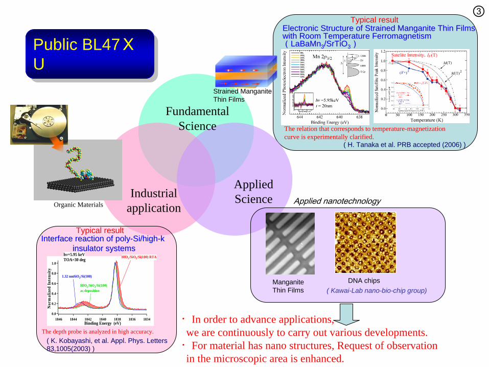
( H. Tanaka et al. PRB accepted (2006) )
1.0
0.8
0.6
0.4
0.2
0.0
Nor
mal
ized
Inte
nsity
1846 1844 1842 1840 1838 1836 1834Binding Energy (eV)
HfO2/SiO2/Si(100) RTA
HfO2/SiO2/Si(100) as deposition
1.32 nmSiO2/Si(100)
h=5.95 keVTOA=30 deg
( K. Kobayashi, et al. Appl. Phys. Letters 83,1005(2003) )
Public BL47X U
Public BL47X U
Interface reaction of polyInterface reaction of poly--Si/highSi/high--k k insulator systemsinsulator systems
Typical result
The depth probe is analyzed in high accuracy.
Electronic Structure of Strained Manganite Thin Films Electronic Structure of Strained Manganite Thin Films with Room Temperature Ferromagnetism with Room Temperature Ferromagnetism ((LaBaMnLaBaMn33 /SrTiO/SrTiO33 ))
Typical result
The relation that corresponds to temperature-magnetization curve is experimentally clarified.
Organic Materials
Strained Manganite Thin Films
・In order to advance applications, we are continuously to carry out various developments.
・For material has nano structures, Request of observation in the microscopic area is enhanced.
③
Applied nanotechnology
( Kawai-Lab nano-bio-chip group)Manganite Thin Films
DNA chips

Outline
2. Introduce focusing optics
K-B Mirror
Present status of V: 40μm H: 30μm
・Wide acceptance angle: ±45°
・Present status of solid angle: ±7°
1. Development of Objective lens
After installation K-B Mirror,Status of beam spot size
⇒φ1μm~submicron
Electronic state of Electronic state of microscopic areamicroscopic area
Achievement the 3D analysis in the chemical states by taking depth profiles and sample scanning.
Purpose④

Development of Beamline SysytemDevelopment of K-B mirror system at BL47XU
In-vacuum" planar undulator, 5.9 ~18.9 keV Si (111) double crystal monochrometer liquid nitrogen cooling (not closed cycle system) Si (333) channel cut
10m
53 m
ID Mono
Front-end slit
0 29 m 36 m 51 m
1st hatch 2nd hatchOptics hatch
44 m 48 m
40.5m
Tc Slit sample
Hypothetical source point
⑤

Hard X-ray Photoemission Spectroscopy – K-B MirrorK-B mirror system
elliptical mirrors; figure errors ~ 2 nm; platinum coating;glancing angle ~ 3 mrad; incident slit: 300×300 μm
350
⑥
This large working distance make possible to realize wide space around sample

Hard X-ray Photoemission Spectroscopy – K-B MirrorFocusing Result
Beam size: 1.1μm (H) × 0.98μm (V)
Using Wire Scan monitor
⑦

Hard X-ray Photoemission Spectroscopy – Objective Lens
About withstanding voltage・・・・ Stable operation under 8kV application for 48 hrs
without discharge.
SIMION trace calculation (for 1kV)
(mm)
Development of Objective Lens
Main feature・・・・ Discharge prevention measures by simplification
of correction electrode part structure・ The shape mesh of a spheroid type・Working Distance=10mm・Magnification factor=5
In Collaborate with Drs. Daimon and Matsuda
⑧

Hard X-ray Photoemission Spectroscopy – Objective Lens
Au3d(3.2keV)Au3d(3.2keV)
Lens mode: angularPE=200eV,Slit:S4.0,FixedBeam Size200um(50W:Crkα
Lab X-ray source)Raster Scan(1mm×1mm)
2D detector Image2D detector Image
Total Acceptance angle of ±32degrees
Angle test device(VG SCIENTA)
X-ray Source
-1.0 0.0 1.0Emission Angle (deg)
3208eV
3206
3204
3202
3200
3198
3196
Kin
etic
Ene
rgy
(eV
)
0035 35
Separation between lines: 2.8degrees
- 35 0 35
Inte
nsity
(arb
.uni
ts)
Emission Angle (deg)Emission angle(deg) Peak width
0 1.1310 1.1725 1.1135 1.53
(Evaluation of acceptance angle)
⑨

X-ray
HAXPES SystemK-B Mirror
X-ray
Analyzer
Objective Lens
Wire scan System
Live showLive show
Objective Lens and K-B Mirror combined with HAXPES system
Hard X-ray Photoemission Spectroscopy in BL47XU2008.7.31
350mm
Translatio n
HAXPES system of BL-47XU
⑩

Hard X-ray Photoemission Spectroscopy(Evaluation of Intensity)
- decreased about 30 times
×10
6
Previous
×10
4
Energy relative to EF (eV)
With K-B
-90 -88 -86 -84 -820.0
0.5
1.0
1.5
2.0
×10
6
With K-B + Lens
- decreased about 0.5 times
Decreasing of flux efficiency by KDecreasing of flux efficiency by K--B mirror can be greatly B mirror can be greatly supplemented with objective lenssupplemented with objective lens
Au4f spectra
・ Attenuation by part Air path (About 1.5m). ※ The K-B system will be examined to replacement with He gas
⑪
3.5×10⁶ 1.8×1061.2×105
Photon Energy=7.94KeVPass Energy=200eVSlit:=C 0.5

Hard X-ray Photoemission Spectroscopy (Evaluation of Energy Resolution) Au Ef spectra
- 1 .0 - 0 .5 0 .0 0 .5
With K-B + Lens
Energy Resolution =255meV
Previous
Inte
nsity
(arb
. uni
ts)
Energy Resolution =237meV
Energy relative to EF (eV)
With K-B
Energy Resolution =217meV
–20meV
Resolution decreases when Object Lens is used.Resolution decreases when Object Lens is used.It results in the aberration (high degree side) due It results in the aberration (high degree side) due to the bend of spheroid shape mesh. to the bend of spheroid shape mesh. ※ Spheroid shape mesh making technology and Spheroid shape mesh making technology and the hole diameter shape are examined. the hole diameter shape are examined. 1
0-1
Emis
sion
Ang
le(d
eg)
7 86 0 eV7 8 567 8 5278 4 8
K ine tic E n erg y (e V)
25
-25
2D detector Image2D detector Image of Angular mode (Au4f)of Angular mode (Au4f)
⑫Photon Energy=7.94KeVPass Energy=200eVSlit:=C 0.5

Hard X-ray Photoemission Spectroscopy (Evaluation of Depth Probing)SiO2 (4nm)/Si spectra
TOA Dependence of Si Oxide
A oxide component increase is confirmed to the surface!
6090 6095 6100 6105
Nor
mal
ized
Inen
sity
Take Off Angle (deg)
Kineitic Energy (eV)
75 65 60 55 50 45 40 35 30 25
Si1s
SiO2
20 30 40 50 60 70 80
Nor
mal
ized
Inte
gral
Inte
nsity
TOA (deg)
1.0
0
-80
-70
-60
-50
-40
-30
-20
Emis
sion
Ang
le (d
eg)
6104610261006098609660946092Kinetic Energy (eV)
2D detector Image2D detector Image of Anglar mode (Si1s)of Anglar mode (Si1s)(Sample Angle 55deg fixed)
The emitted electron angle and depth information can be acquired without changing the angle of the sample.
TOA(deg)Kinetic Energy(eV)
10 min acquisition
TOA dependence of Si1s from SiO2Normalized by substrate Si1s intensity
One Detector Image
⑬Photon Energy=7.94KeVPass Energy=200eVSlit:=C 0.5

Hard X-ray Photoemission Spectroscopy
7800 7820 7840 78600
500
1000
1500
2000
2500
3000
3500Si2s
Au4f
Inte
nsity
(arb
.uni
ts)
Kinetic Energy (eV)
7800 7820 7840 78600
500
1000
1500
2000
2500
3000
Si2s
Au4f
Inte
nsity
(arb
.uni
ts)
Kinetic Energy (eV)
7800 7820 7840 78600
5001000150020002500300035004000450050005500
Si2s
Au4f
Inte
nsity
(arb
.uni
ts)
Kinetic Energy (eV)
Au(μ-dot) /Si
Au (t=20nm)
10μm
5μm
Si substrate
2D mapping of Au pattern on Si substrate by Sample Scanning2D mapping of Au pattern on Si substrate by Sample Scanning
⑭
Step size= 10μm

Hard X-ray Photoemission Spectroscopy ( 2D mapping)
140
120
100
80
60
40
20
0
604020
600
0
5500
5500
5000
4500
4000 3500
3000 2500
2000
1500
1000
500
140
120
100
80
60
40
20
0
100806040200
6500
6500
600
0
600
0
5500
5500 5500
5000 4500 4000
3500
3000
2500
2000 1500
1000 1000
500
500
Au4f Si2s
X-axis (μm) Z-axis (μm) X-axis (μm) Z-axis (μm)
μm μm
Spatial Resolution= 1μm
⑮

Hard X-ray Photoemission Spectroscopy
(1) Objective Lens
・Total Acceptance angle = ±32 degrees
(2) K-B mirror
・Beam Size = Φ1μm
(3) Combination
・3D chemical states Mapping is possible now!
Summary
⑯