Guide · str-a6051m 67 khz 650 v 3.95Ω 20 w 16 w 30 w 21 w str-a6052m 2.8Ω 23 w 19 w 35 w 25 w...
52
P.1 ACDC-SGE 2015.01.29 AC/DC Convertor Power Factor Control (PFC) IC Guide The To place orders or request samples, please contact distributor Profusion plc: [email protected] all contents in this document are as of date of publica on. Make sure that this is the latest revision of the document before use. Please check the details of the product by data sheet. h p://www.sanken-ele.co.jp/en
Transcript of Guide · str-a6051m 67 khz 650 v 3.95Ω 20 w 16 w 30 w 21 w str-a6052m 2.8Ω 23 w 19 w 35 w 25 w...

P.1ACDC-SGE 2015.01.29
AC/DC Convertor
Power Factor Control (PFC) IC
Guide
TheTo place orders or request samples, please contact distributor Profusion plc:[email protected]
all contents in this document are as of date of publica on.Make sure that this is the latest revision of the document beforeuse. Please check the details of the product by data sheet.h p://www.sanken-ele.co.jp/en

P.2ACDC-SGE 2015.01.29
CONTENTS
Selection Guide of Power Management IC by Control Topology P.3
Selection Guide by Application P.4
For Low Power Application P.5
For Low and Middle Power Application P.6
For High Power Application P.7
Power Supply ICs P.8
• PWM control IC P.9
• PRC control IC P.309
• QR control IC P.32
• LLC control IC P.41
• PFC control IC P.46
IMPORTANT NOTES P.51

P.3ACDC-SGE 2015.01.29
Output Power
PO < 75W
PO ≥75W
Input Power at No Load
PWM IC
< 25mW
Component Count and Noise Requirement
LLC IC
Quasi-Resonant IC
For low component count
PWM IC
Component Count and Noise Requirement
For low noiseLLC IC
For low noise and low component count
Quasi-Resonant IC
PFC IC
PRC IC
PFC IC
Selection Guide of Power Management IC by Control Topology
START
≥25mW
For low noise
For low noise and low component count
PO ≥25W
PO <25W
→P.9
→P.41
→P.46
→P.32
→P.29→P.9
→P.32
→P.46
→P.39

P.4ACDC-SGE 2015.01.29
Selection Guide by ApplicationBack to contents
PFCPower Factor Correction
PRC Low Noise
Fixed Off-time Control
PWM Small Circuit
Pulse Width Modulation
Fixed Frequency Control
QR Low Noise
Quasi-Resonant Mode
Variable Frequency Control
LLC Low Noise
Current Resonance Mode
→P.9
→P.32
→P.41→P.46
→P.29

P.5ACDC-SGE 2015.01.29
AC/DC Convertor
VAC Cont.
VOUT
(-)
(+)
AC/DC Convertor
VAC Cont.
VOUT
(-)
(+)
For Low Power Application OFF Line Controllers with Integrated Power MOSFET and the Peripheral Diodes
PWM IC Power supply for small consumer electronics and motor control,and auxiliary power supply for lighting etc.
Off Line Controllers
Freewheel Diode
→STR5A400 Series P.27
Buck Convertor Buck-boost Convertor
*See Selection Guide of Diode about peripheral diodes.
Back to contents

P.6ACDC-SGE 2015.01.29
Power Management IC
VAC
Cont.
Photo lsolator
FB GND
VOUT
GND
Error
Amp.
For Low and Middle Power ApplicationOFF Line Controllers with Integrated Power MOSFETand the Peripheral Diodes
PWM IC
Diode for Snubber
Diode for Secondary
Rectification
PRC IC
QR IC
Off Line Controllers
For low power application : Auxiliary power supply, white goods and adapter etc.
For low and middle power application : White goods etc.
For middle power application : White goods and OA etc.
Back to contents
→P.32
→P.29
→P.9
*See Selection Guide of Diode about peripheral diodes.

P.7ACDC-SGE 2015.01.29
VAC
PFCControl IC
Photo lsolator
Control IC for Auxiliary power supply
VOUT2
Cont.
Photo lsolator
GNDFB
LLC Control IC
FB GND
REG
VS
Error
Amp.
Error
Amp.
VOUT1
Diode for PFC
Boot Strap Diode
For High Power ApplicationPFC and OFF Line Controllers and the Peripheral Diode
PWM IC
LLC IC
PFC IC
For high power application, industrial equipment, etc.
Power Factor CorrectionDiode for Secondary
Rectification
For auxiliary power supply
Back to contents
Diode for Snubber
→P.41
→P.46
→P.9
*See Selection Guide of Diode about peripheral diodes.

P.8ACDC-SGE 2015.01.29
Control topology
MOSFET PO
Small circuit
PIN at noload
Noise Control method Page
PWM Built-in Low ◎ ◎ △ Fixed frequency P.9
PRC Built-in ○ ○ ○ Fixed off time (Variable frequency)
P.29
Quasi-Resonant
Built-in ○ ○◎
Bottom-on control
Variable frequency P.32
LLC External High △ △◎
Soft switching control
Current resonance P.41
Power Supply ICs
Lineup of the power supply IC by control topology. Please refer to Sanken’s website for detail information.
MOSFET PO Control method Page
PFC External ≥75W Interleaved Discontinuous Conduction Mode (DCM) Operation Continuous Conduction Mode(CCM) Operation Critical Conduction Mode (CRM) Operation
P.46
Back to contents

P.9ACDC-SGE 2015.01.29
OFF Line PWM Controllerswith Integrated Power MOSFET
Control Method Series PackageNo load power consumption
Feature Page
Flyback(Secondary side regulation)
STR-W6000 TO-220F-6L < 30 mW Brown in / out P.11
STR-A6000DIP8
< 25 mW
Brown in / outP.13
STR-V653SIP8L Brown in / out
High reliability and low profile packageP.15
STR2W100DTO-220F-6L
P.17
STR3A100DIP8
< 15 mW
Low thermal resistance packageP.19
STR3A400DIP8 Low thermal resistance package
Improving light load efficiencyP.21
STR4A100DIP8 / SOIC8
< 10 mW1chip structureBuilt in OCP detection resistor
P.23
Flyback(Primary side regulation)
STR5A100DDIP8
< 30 mW1chip structureBuilt in OCP detection resistor
P.25
Non-isolatedBuck/ Buck-boost
STR5A400DDIP8 / SOIC8
-1chip structureBuilt in OCP detection resistor
P.27
For low power, auxiliary power supply, white goods and adapter etc Low standby power and low component count PWM : Pulse Width Modulation, fixed frequency control
Back to contents

P.10ACDC-SGE 2015.01.29
White Goods,
Adapter
Low Power White
Goods
10 20 30 40 50 60 70 80
Maximum Output power (Open frame, Universal) (W)
Low power consumption at no load Low component count Green mode (STR5A100D)
STR4A100
STR-A6000
Line Undervoltage Protection (Brown-In / out)
High Reliability package (STR-V653) STR-W6000
STR5A100D (Primary Side Sensing)
Non-isolation type Low component count Green mode
Low Thermal Resistance DIP8 Package Low power consumption at no load Low component count STR3A400 achieves CoC Tier 2 and
DoE propose
STR5A400 (Buck / Buck boost )
STR3A400
PWM control IC Selection Guide
STR2W100
STR-V653
Aar conditioner
Refrigerator
Adapter
Washing machine
microwave oven
Rice cooker
Cleaner
→P.23
→P.19
→P.13
→P.15 →P.17
→P.11
→P.25
→P.27
→P.21
STR3A100

P.11ACDC-SGE 2015.01.29
No load power consumption < 30 mW
Brown-in and Brown-out Function
Protections
OCP is pulse by pulse
OLP, OVP and TSD are all restart
Lineup
Part Number fOSCMOSFET POUT
VDSS RDS(ON) AC230V Universal
STR-W6051S
67 kHz650 V
3.95 Ω 45 W 30 W
STR-W6052S 2.8 Ω 60 W 40 W
STR-W6053S 1.9 Ω 90 W 60 W
STR-W6072S 800 V 3.6 Ω 50 W 32 W
STR-W6000 Series
PIN < 30 mW at no load, PWM Off-Line Switching Regulators
PackageTO-220F-6L

P.12ACDC-SGE 2015.01.29
Pin assignment
PackageTO-220F-6L
Pin No. Symbol Function
1 D/STMOSFET Drain and startup current input
3 S/OCP MOSFET Source and Overcurrent Protection
4 VccPower supply input and Overvoltage Protection
5 GND Ground
6 FB/OLPFeedback control and Overload Protection
7 BR Brown-in and Brown-out control
STR-W6000 Series
PIN < 30 mW at no load, PWM Off-Line Switching Regulators
Features Brown-in and Brown-out FunctionNo load power Consumption < 30mW Auto Standby Function
Normal operation : PWM modeStandby operation: Burst oscillation mode
Audible noise suppression function for standby mode Bias Assist Function Random Switching Function
Slope Compensation Function Leading Edge Blanking Function Two chip structure (avalanche energy guaranteed) Protection
- Overcurrent Protection (OCP) : Pulse by pulse, with input compensation circuit
- Overload Protection (OLP) : Auto restart with delay timer- Overvoltage Protection (OVP) : Auto restart- Thermal Shutdown (TSD) : Auto restart
VAC
C1 C6 R1
D1
D2 R2
C2
T1D51
C51
R51
R52
U51
R54
R56
C52
D
P
S
PC1
PC1
C3
ROCP
CY
BR1
R53
R55
L51
C53
C5
BR
GN
D
FB
/OL
P
S/O
CP
VC
C
D/S
T
2
1 7653 4
STR-W6000S
U1
RC
C4
RA
RB
TC_STR-W6000S_1_R1
VOUT(+)
VOUT(-)
Typical application circuit

P.13ACDC-SGE 2015.01.29
Part Number fOSCMOSFET POUT (Adapter) POUT (Open frame)
VDSS RDS(ON) AC230V Universal AC230V Universal
STR-A6051M
67 kHz650 V
3.95 Ω 20 W 16 W 30 W 21 W
STR-A6052M 2.8 Ω 23 W 19 W 35 W 25 W
STR-A6053M 1.9 Ω 26 W 22 W 41 W 29 W
STR-A6079M 800 V 19.2 Ω 8 W 6 W 13 W 9 W
STR-A6059H
100 kHz
650 V 6.0 Ω 17 W 11 W 30 W 19 W
STR-A6069H
700 V
6.0 Ω 17 W 11 W 30 W 19 W
STR-A6061H 3.95 Ω 21 W 15 W 35 W 24 W
STR-A6062H 2.8 Ω 23 W 18 W 38 W 26 W
STR-A6069HD
100 kHz 700 V
6.0 Ω 17 W 11 W 30 W 19 W
STR-A6061HD 3.95 Ω 21 W 15 W 35 W 24 W
STR-A6062HD 2.8 Ω 23 W 18 W 38 W 26 W
STR-A6063HD 2.3 Ω 25 W 20 W 40 W 27 W
Lineup
No load power consumption < 25 mW
Brown-in and Brown-out Function
Protections
OCP is pulse by pulse (The products with suffixed “D” have two OCP types)
OLP is auto restart
OVP and TSD are latched shutdown
STR-A6000 Series
PIN < 25 mW at no load, PWM Off-Line Switching Regulators
PackageDIP8

P.14ACDC-SGE 2015.01.29
Pin No. Symbol Function
1 S/OCP MOSFET Source and Overcurrent Protection
2 BR Brown-in and Brown-out control
3 GND Ground
4 FB/OLP Feedback control and Overload Protection
5 VCCPower supply input and Overvoltage Protection
6 - (Pin removed)
7D/ST MOSFET Drain and startup current input
8
Pin assignment
Package
DIP8
STR-A6000 Series
PIN < 25 mW at no load, PWM Off-Line Switching Regulators
Features Brown-in and Brown-out FunctionNo Load Power Consumption < 25mW Auto Standby Function
Normal operation : PWM modeStandby operation: Burst oscillation mode
Audible noise suppression function for standby mode Bias Assist Function Random Switching Function Slope Compensation Function Leading Edge Blanking Function
Two chip structure (avalanche energy guaranteed) Protections
- Overcurrent Protection (OCP)*: Pulse by pulse, with input compensation circuit
- Overload Protection (OLP) : Auto restart with delay timer- Overvoltage Protection (OVP) : Latched shutdown- Thermal Shutdown (TSD) : Latched shutdown
*The products suffixed D have an additional OCP function which operates during leading edge blanking period, to operate as protection at the condition such as output windings shorted or unusual withstand voltage of secondary-side diodes.
VAC
C1
C6 R1
D1
BR1
R2
C2
T1
D
P
PC1C3
ROCP CY
C5
1 2 3 4
D/ST D/ST
BR
NC
S/OCP FB/OLPGND
VCC
8 7 5
STR-A6000U1
D2
C4RC
RB
RA
D51
C51
R51
R52
U51
R54
R56
C52
S
PC1
R53
R55
L51
C53
VOUT
(+)
TC_STR-A6000_1_R1
(-)
Typical application circuit

P.15ACDC-SGE 2015.01.29
No load power consumption < 25 mW
Brown-in and Brown-out Function
High reliability and low profile packageHeight ≤ 12 mm, pin pitch = 2.54 mm,creepage distance between high voltage pin and low voltage pin ( > 4 mm)
Protections
OCP is pulse by pulse
OLP is auto restart
OVP and TSD are latched shutdown
Part Number fOSCMOSFET POUT
VDSS RDS(ON) AC230V Universal
STR-V653 67 kHz 650 V 1.9 Ω 30 W 23 W
STR-V653
High Reliability and Low Profile PackagePWM Switching Power Supply Applications
PackageSIP8L
Lineup

P.16ACDC-SGE 2015.01.29
Pin assignment
Package
SIP8L
Pin No. Symbol Function
1 D/ST MOSFET Drain and startup current input
3 S/OCPMOSFET Source and Overcurrent Protection
4 BR Brown-in and Brown-out control
5 GND Ground
6 FB/OLPFeedback control and Overload Protection
8 VCCPower supply input and Overvoltage Protection
FeaturesHigh reliability and low profile package Brown-in and Brown-out FunctionNo load power consumption < 25mW Random Switching Function Built-in startup circuit Bias Assist Function Slope Compensation Function Auto Standby Function
Leading Edge Blanking Function Audible noise suppression function for standby mode Two chip structure (avalanche energy guaranteed) Protections
- Overcurrent Protection (OCP) : Pulse by pulse, with input compensation circuit
- Overload Protection (OLP) : Auto restart with delay timer- Overvoltage Protection (OVP) : Latched shutdown- Thermal Shutdown (TSD) : Latched shutdown
STR-V653
High Reliability and Low Profile PackagePWM Switching Power Supply Applications
Typical application circuit

P.17ACDC-SGE 2015.01.29
No load power consumption < 25 mW
Protections
OCP is pulse by pulse
OLP, OVP and TSD are all auto restart
Part Number fOSCMOSFET POUT
VDSS RDS(ON) AC230V Universal
STR2W152D67 kHz 650 V
3.0 Ω 60 W 40 W
STR2W153D 1.9 Ω 90 W 60 W
Lineup
STR2W100D Series
PIN < 25 mW at no load, PWM Off-Line Switching Regulators
PackageTO-220F-6L

P.18ACDC-SGE 2015.01.29
Pin No. Symbol Function
1 D/STMOSFET Drain and startup current input
3 S/OCP MOSFET Source and Overcurrent Protection
4 VCCPower supply input and Overvoltage Protection
5 GND Ground
6 FB/OLPFeedback control and Overload Protection
7 NC ―
Pin assignment
Package
TO-220F-6L
STR2W100D Series
PIN < 25 mW at no load, PWM Off-Line Switching Regulators
FeaturesNo load power consumption < 25mW Auto Standby Function
Normal operation : PWM modeStandby operation: Burst oscillation mode
Soft Start Function Bias Assist Function Random Switching Function Slope Compensation Function
Leading Edge Blanking Function Two chip structure (avalanche energy guaranteed) Protections
- Overcurrent Protection (OCP) : Pulse by pulse, with input compensation circuit
- Overload Protection (OLP) : Auto restart with delay timer- Overvoltage Protection (OVP) : Auto restart- Thermal Shutdown (TSD) : Auto restart
VAC
C1
D2 R2
C2
T1D4
C6
R4
R5
U2
R9
R7
C7
D
P
S
PC1
PC1C3ROCP C9
D1
R6
R8
L2
C8
VOUT
GND
NC
GN
D
FB
/OL
P
S/O
CP
VC
C
D/S
T
2
1 7653 4
STR
2W100D
U1
Typical application circuit

P.19ACDC-SGE 2015.01.29
No load power consumption < 15 mW
Low thermal resistance package
Protections
OCP is pulse by pulse
OLP is auto restart
OVP and TSD are latched shutdown or auto restart
Lineup
STR3A100 Series
PIN < 15 mW at no load, PWM Off-Line Switching Regulators
PackageDIP8
Products OVP / TSD Operation
STR3A1xx Latched shutdown
STR3A1xxDSTR3A1xxHD
Auto restart
fOSC Part NumberMOSFET POUT (Adapter) POUT (Open frame)
VDSS(min.) RDS(ON) (max.) AC230V Universal AC230V Universal
67 kHz
STR3A151
650 V
4.0 Ω 29.5 W 19.5 W 37 W 23 WSTR3A151D
STR3A1523.0 Ω 33 W 23.5 W 45 W 29 W
STR3A152D
STR3A1531.9 Ω 37 W 27.5 W 53 W 35 W
STR3A153D
STR3A154 1.4 Ω 41 W 31 W 60 W 40 W
STR3A1551.1 Ω 45 W 35 W 65 W 44 W
STR3A155D
100 kHz
STR3A161HD
700 V
4.2 Ω 25 W 20 W 36 W 24 W
STR3A162HD 3.2 Ω 28 W 23 W 40 W 28 W
STR3A163HD 2.2 Ω 32 W 25.5 W 46 W 33.5 W

P.20ACDC-SGE 2015.01.29
Features Low thermal resistance packageNo load power consumption < 15mW Auto Standby Function
Normal operation : PWM modeStandby operation: Burst oscillation mode
Soft Start Function Bias Assist Function Random Switching Function
Slope Compensation Function Leading Edge Blanking Function Two chip structure (avalanche energy guaranteed) Protections
- Overcurrent Protection (OCP) : Pulse by pulse, with input compensation circuit
- Overload Protection (OLP) : Auto restart with delay timer- Overvoltage Protection (OVP) : Latched shutdown or auto restart- Thermal Shutdown (TSD) : Latched shutdown or auto restart
STR3A100 Series
PIN < 15 mW at no load, PWM Off-Line Switching Regulators
Typical application circuit
Pin No. Symbol Function
1 S/OCP MOSFET Source and Overcurrent Protection
2 VCC Power supply input and Overvoltage Protection
3 GND Ground
4 FB/OLP Feedback control and overload Protection
5
D/ST MOSFET Drain and startup current input6
7
8
Pin assignment
VAC
C1
C5 R1
D1
D2 R2
C2
T1 D51
C51
R51
R52
U2
R54
R56
C52
D
P
S
PC1
PC1
C3ROCP
BR1
R53
R55
L51
C53
C4
VOUT
GND
1 2 3 4
D/ST D/ST
VCC
NC
S/OCP FB/OLPGND
D/ST D/ST
8 7 6 5
STR3A100U1
CY
PackageDIP8

P.21ACDC-SGE 2015.01.29
STR3A400 Series
PIN < 15 mW at no load, PWM Off-Line Switching Regulators
fOSC Part NumberMOSFET POUT (Adapter) POUT (Open frame)
VDSS(min.) RDS(ON) (max.) AC230V Universal AC230V Universal
65 kHz
STR3A451
650 V
4.0 Ω 29.5 W 19.5 W 37 W 23 WSTR3A451D
STR3A4531.9 Ω 37 W 27.5 W 53 W 35 W
STR3A453D
STR3A455D 1.1 Ω 45 W 35 W 65 W 44 W
Line up
Improving efficiency in all load area achieves energy efficiency regulations of EPS* (EU: CoC Tier 2, U.S.: DoE propose)
No load power consumption < 15mW
Low thermal resistance package
Protections
OCP is pulse by pulse, built-in two OCP types
OLP is auto restart
OVP and TSD are latched shutdown or auto restart
PackageDIP8
Products OVP / TSD OperationSTR3A4xx Latched shutdownSTR3A4xxD Auto restart
UD
UD
UD
UD
UD : Under developmentUD
*EPS: External Power Supply

P.22ACDC-SGE 2015.01.29
Features For CoC Tier 2 and DoE propose Low thermal resistance package Auto Standby Function
No load power consumption < 15mWOperation mode
Normal operation : PWM ModeLight load operation : Green-ModeStandby operation: Burst oscillation mode
Soft Start Function
Pin No. Symbol Function
1 S/OCP MOSFET Source and Overcurrent Protection
2 VCC Power supply input and Overvoltage Protection
3 GND Ground
4 FB/OLP Feedback control and overload Protection
5
D/ST MOSFET Drain and startup current input6
7
8
Pin assignment
Bias Assist Function Random Switching Function Slope Compensation Function Leading Edge Blanking Function Two chip structure (avalanche energy guaranteed) Protections
- Overcurrent Protection (OCP) : Pulse by pulse, built-in two OCP types- Overload Protection (OLP) : Auto restart- Overvoltage Protection (OVP) : Auto restart or latched shutdown- Thermal Shutdown (TSD) : Auto restart with hysteresis or latched shutdown
PackageDIP8
STR3A400 Series
PIN < 15 mW at no load, PWM Off-Line Switching Regulators
Typical application circuit
VAC
C1
C5 R1
D1
D2 R2
C2
T1 D51
C51
R51
R52
U2
R54
R56
C52
D
P
S
PC1
PC1
C3ROCP
BR1
R53
R55
L51
C53
C4
VOUT
GND
1 2 3 4
D/ST D/ST
VCC
NC
S/OCP FB/OLPGND
D/ST D/ST
8 7 6 5
STR3A400U1
CY
TC_STR3A400_1_R1

P.23ACDC-SGE 2015.01.29
No load power consumption < 10 mW
High voltage sense MOSFET
One chip structure (Eliminating external components)
VD/ST (max.) = 730 V
Protections
OCP is pulse by pulse
OVP, OLP and TSD are all auto restart
Part Number PKG fOSCMOSFETRDS(ON)
IDLIM(H)
POUT (Adapter) POUT (Open frame)
AC230V Universal AC230V Universal
STR4A162S SOIC8
65 kHz24.6 Ω 0.365 A
5 W 4 W 7 W 5.5 W
STR4A162D DIP8 5.5 W 4.5 W 7.5 W 6 W
STR4A164D DIP8 12.9 Ω 0.520 A 8 W 6 W 10 W 8.5 W
STR4A164HS SOIC8100 kHz 12.9 Ω 0.485 A
8.5 W 6.5 W 12 W 9.5 W
STR4A164HD DIP8 9 W 7 W 13 W 10.5 W
STR4A100 Series
PIN < 10 mW at no load, PWM Off-Line Switching Regulators
UD
Lineup UD : Under developmentUD
PackageDIP8 SOIC8

P.24ACDC-SGE 2015.01.29
Pin No. Symbol Function
1 FB/OLPFeedback control and Overload Protection
2 VCCPower supply input and Overvoltage Protection
3 ― (Pin removed)
4 D/STMOSFET Drain and startup current input
5
S/GND MOSFET Source and ground6
7
8
Pin assignment
FeaturesHigh voltage sense MOSFET One chip structure (eliminating external components)No load power consumption < 10 mW Auto Standby Function
Normal operation : PWM modeStandby operation: Burst oscillation mode
Soft Start Function Bias Assist Function
Random Switching Function Slope Compensation Function Leading Edge Blanking Function Protections
- Overcurrent Protection (OCP) : Pulse by pulse, with input compensation circuit
- Overload Protection (OLP) : Auto restart with delay timer- Overvoltage Protection (OVP) : Auto restart- Thermal Shutdown (TSD) : Auto restart
STR4A100 Series
PIN < 10 mW at no load, PWM Off-Line Switching Regulators
Typical application circuitPackageDIP8 SOIC8

P.25ACDC-SGE 2015.01.29
Part Number fOSCMOSFETRDS(ON)
IDLIM(H)
POUT (Adapter) POUT (Open frame)
AC230V Universal AC230V Universal
STR5A162D 65 kHz
24.6 Ω 0.285 A 4 W 3.5 W 5 W 4.5 W
STR5A164D 13 Ω 0.41 A 6.0 W 5.5 W 8.5 W 7 W
STR5A100D Series
PIN < 30 mW at no load,Primary Side Regulation PWM Off-Line Switching Regulators
No load power consumption < 30mW
High efficiency in light load (Green-mode)
Few external components count
Primary side regulation (no photo-coupler)
One chip structure
High voltage sense MOSFET
VD/ST (max.) = 730 V
Protections
OCP is pulse by pulse
OVP and TSD are auto restart
Lineup
PackageDIP8

P.26ACDC-SGE 2015.01.29
Pin assignment
Features Primary side regulation (no photo-coupler)High voltage sense MOSFET One chip structure (eliminating external components)No load power consumption < 30mW Auto Standby Function
Normal operation : PWM modeLight load operation : Green-modeStandby operation: Burst oscillation mode
Built-in startup circuit Random Switching Function Leading Edge Blanking Function Protections
- Overcurrent Protection (OCP) : Pulse by pulse- Overvoltage Protection (OVP) : Auto restart- Thermal Shutdown (TSD) : Auto restart
Pin No. Symbol Function
1 FB Feedback control
2 VCCPower supply input and Overvoltage Protection
3 ― (Pin removed)
4 D/STMOSFET Drain and startup current input
5
S/GND MOSFET Source and ground6
7
8 COMP Input of phase compensation
PackageDIP8
STR5A100D Series
PIN < 30 mW at no load, Primary Side Regulation PWM Off-Line Switching Regulators
VAC
C1
R1
D1
T1
D
P
C5
C4
C3
R6
R3
R5
D2
BR1
COMP
S/GND VCC
NC
FB
D/ST
S/GND
S/GND
8
7
6
5
STR5A100D
U1
1
2
4
R2
L1
C2
R4
D50
S1
VOUT
GND
C52
C51R51
C6
R7
R52
Typical application circuit

P.27ACDC-SGE 2015.01.29
Non-isolated buck and buck-boost converter solution
Positive or negative output configuration
High efficiency in light load (Green-mode)
Few external components count
High voltage sense MOSFET
Build-in error amplifier
VD/ST (max.) = 700 V
ProtectionsOLP, OVP and TSD are all auto restart
Part Number Package fOSCMOSFETRDS(ON)
IDLIM
STR5A462D DIP8 60 kHz
26 Ω 0.285 A
STR5A464D 13.6 Ω 0.41 A
STR5A462S SOIC8 60 kHz
26 Ω 0.285 A
STR5A464S 13.6 Ω 0.41 A
Lineup : Under developmentUD
UD
UD
UD
STR5A400 Series
High EfficientOff-Line PWM Buck and Buck-boost Convertor
PackageDIP8 SOIC8

P.28ACDC-SGE 2015.01.29
Pin assignment
Typical application circuit・Buck convertor
(Positive output)
FeaturesHigh voltage sense MOSFET One chip structure (eliminating external components) Auto Standby Function
Normal operation : PWM modeLight load operation : Green-modeStandby operation: Burst oscillation mode
Build-in error amplifier Built-in startup circuit Leading Edge Blanking Function Protection
- Overload Protection (OLP) : Auto restart with delay timer- Overvoltage Protection (OVP) : Auto restart- Thermal Shutdown (TSD) : Auto restart
VAC
VOUT
SVCC
NC
FB
D/ST
S
S
8
7
6
5
STR5A400D
4
2
1
C2
C4R1 C3
R2 R3
C5
C6 R4D3
D2D1
L2L1
C1
S
+
-
BR1
VOUT
SVCC
NC
FB
D/ST
S
S
8
7
6
5
STR5A400D
4
2
1
C2
C4R1 C3
R2 R3
C5
C6 R4
D3
D2D1
L2
L1
C1
S
-
+
VAC
BR1
・Buck-boost convertor(Negative output)
SymbolPin No.
FunctionDIP8 SOIC8
FB 1 2Constant voltage control signal input
VCC 2 1
Power supply voltage input for control part and Overvoltage Protection signal input
― 3 (Pin removed)
D/ST 4MOSFET Drain and startup current input
S 5 ~ 8 MOSFET Source and ground
STR5A400 Series
High EfficientOff-Line PWM Buck and Buck-boost Convertor
PackageDIP8 SOIC8

P.29ACDC-SGE 2015.01.29
Series PackageNo Load Power
Consumption (PIN)Page
STR-V100SIP8L
< 40 mW P.30
OFF Line PRC Controllerswith Integrated Power MOSFET
For low and middle power application : White goods etc.
PRC: Pulse Ratio Control(Controlling on-time under fixed off-time)
Back to contents

P.30ACDC-SGE 2015.01.29
Part NumberMOSFET
t(OFF)
POUT
Auto BiasVDSS RDS(ON) AC220V Universal
STR-V152
650 V
2.8 Ω 8 μs 22 W 17 W Yes
STR-V153 2.0 Ω 11.5 μs 30 W 23 W No
High reliability and low profile packageHeight ≤ 12 mm, pin pitch = 2.54 mm,creepage distance between high voltage pin and low voltage pin ( > 4 mm)
No load power consumption < 40mW Protections
OCP is pulse by pulse OLP is auto restart OVP and TSD are latched shutdown
PackageSIP8L
Lineup
STR-V100 Series
High Reliability and Low Profile PackagePRC Off-Line Switching Regulators

P.31ACDC-SGE 2015.01.29
Pin No. Symbol Function
1 D MOSFET Drain
2 - -
3 S/OCPMOSFET Source and Overcurrent Protection signal input
4 VCCFeedback controlOver Load Protection
5 GND Ground
6 FB/OLPFeedback control and Overload Protection signal input
7 - -
8 Startup Startup current input
Pin assignment
Package
SIP8L
STR-V100 Series
High Reliability and Low Profile PackagePRC Off-Line Switching Regulators
FeaturesHigh reliability and low profile package No load power consumption < 40 mW Built-in startup circuit Auto Bias Function Auto Standby Function Leading Edge Blanking Function
Two chip structure (avalanche energy guaranteed) Protections
- Overcurrent Protection (OCP): Pulse by pulse- Overload Protection (OLP): Auto restart- Overvoltage Protection (OVP) : Latched shutdown- Thermal Shutdown (TSD): Latched shutdown
Typical application circuit

P.32ACDC-SGE 2015.01.29
Off-Line Quasi-Resonant (QR) Controllers with Integrated Power MOSFET For middle power application: White goods and OA, etc.
High efficiency operation across the full range of loads is achieved by multi-mode control
Low noise due to bottom on switching
Back to contents
Series packagePo
(AC230V)Feature Page
STR-Y6700
TO-220F-7L
~140W Low power consumption at No Load ( < 0.5 W) Few external components count (Built-in startup circuit) Thermal shutdown (TSD)
P.33
STR-L6400
SIP10L
~25W
High Reliability and Low Profile Package Low power consumption at No Load ( < 0.1 W) External ON / OFF Function Few external components count (Built-in startup circuit) Thermal shutdown (TSD)
P.35
STR-W6700
TO-220F-6L
~150W Various startup sequence control
(External startup Resistor )P.37
STR-X6700
TO-3PF-7L
~200W Various startup sequence control
(External startup Resistor )P.39

P.33ACDC-SGE 2015.01.29
High efficiency operation across the full range of loads is achieved by multi-mode control
No load power consumption < 30 mW (AC 100 V)
Protections
OCP is pulse by pulse
OLP, OVP and TSD are latched shutdown
PackageTO-220F-7L
Lineup
STR-Y6700 Series
Low Noise, No Load Power Consumption < 30mWQuasi-resonant (QR) Off-Line Switching Regulators
Part NumberMOSFET POUT
VDSS RDS(ON) DC 380 V Universal
STR-Y6735*500 V 0.8 Ω
AC 100 V120 W
―STR-Y6735A
STR-Y6753*650 V
1.9 Ω 100 W 60 W
STR-Y6754* 1.4 Ω 120 W 67 WSTR-Y6763*
800 V
3.5 Ω 80 W 50 WSTR-Y6763A
STR-Y6765* 2.2 Ω 120 W 70 W
STR-Y6766*1.7 Ω 140 W 80 W
STR-Y6766A
* The IC has higher threshold OCP for an abnormal state, such as an output winding being shorted. This overcurrent protection also operates during the leading edge blanking and stops a switching operation in latch mode .

P.34ACDC-SGE 2015.01.29
Package
TO-220F-7L
STR-Y6700 Series
Low noise, No Load Power Consumption < 30mWQuasi-resonant (QR) Off-Line Switching Regulators
Pin assignment Pin No. Symbol Function
1 D/ST MOSFET Drain and start-up current input
2 S/OCPMOSFET Source and Overcurrent Protection signal input
3 VCCPower supply input and Overvoltage Protection signal input
4 GND Ground
5 FB/OLPFeedback control and Overload Protection signal input
6 BDBottom detection signal input and input compensation detection signal input
7 NF ―
FeaturesNo load power consumption
< 30 mW (AC100V), < 50 mW (AC230V)Multi-mode control
Normal QR operation ~ one bottom-skip QR operation ~ burst operation
Built-in Startup circuit Soft Start Function Bias Assist Function
Maximum on-time limiting Leading Edge Blanking Function Two chip structure (avalanche energy guaranteed) Protections
- Overcurrent Protection (OCP) : Pulse by pulse, with input compensation circuit
- Overload Protection (OLP) : Latched shutdown - Overvoltage Protection (OVP) : Latched shutdown - Thermal Shutdown (TSD) : Latched shutdown
Typical application circuit

P.35ACDC-SGE 2015.01.29
High efficiency operation across the full range of loads is achieved by multi-mode control
No load power consumption < 0.1 W
High reliability and low profile packageHeight ≤ 12 mm, pin pitch = 2.54 mm,creepage distance between high voltage pin and low voltage pin ( > 6mm)
External ON/OFF Function
Protections
OCP is pulse by pulse
OLP, OVP and TSD are latched shutdown
PackageSIP10L
Part NumberMOSFET POUT Protection Functions
VDSS RDS(ON) AC100V AC240V OCP OVP OLP TSD
STR-L6472 850 V 6.5 Ω 15 W 25 WPulse by
pulseLatch
shutdownLatch
shutdownLatch
shutdown
Lineup
STR-L6472
Low noise, High Reliability and Low Profile PackageQuasi-resonant (QR) Off-Line Switching Regulators

P.36ACDC-SGE 2015.01.29
Package
SIP10L
STR-L6472
Pin assignment
Pin No. Symbol Function
1 D/Startup MOSFET Drain and start-up current input
2 S/GND MOSFET Source and ground
3 VCCPower supply input and Overvoltage Protection signal input
4 FBFeedback control and Overload Protection signal input
5 BDBottom detection signal input and input compensation detection signal input
6 OCPOvercurrent Protection signal input and bottom-skip signal input
7 ADJSoft start control and Bottom-skip delay time control and remote ON/OFF signal input
FeaturesHigh reliability and low profile package No load power consumption < 0.1 WMulti-mode control
Normal QR operation ~ one bottom-skip QR operation ~ burst operation
Built-in Startup Circuit Soft Start Function External ON/OFF Function
Maximum on-time limiting Leading Edge Blanking Function Two chip structure (avalanche energy guaranteed) Protections
- Overcurrent Protection (OCP) : Pulse by pulse, with input compensation circuit
- Overload Protection (OLP) : Latched shutdown - Overvoltage Protection (OVP) : Latched shutdown - Thermal Shutdown (TSD) : Latched shutdown
Low noise, High Reliability and Low Profile PackageQuasi-resonant (QR) Off-Line Switching Regulators
Typical application circuit

P.37ACDC-SGE 2015.01.29
High efficiency operation across the full range of loads is achieved by multi-mode control
Have a wide choice of variations
External startup resistor Various startup sequence control can be selected
Protections
OCP is pulse by pulse
OVP and OLP are latched shutdown
STR-W6700 Series
LineupPackageTO-220F-6L
Low NoiseQuasi-resonant (QR) Off-Line Switching Regulators
Part NumberMOSFET
VDSS RDS(ON)
STR-W6723N 450 V 1.4 Ω
STR-W6734
500 V
1 Ω
STR-W67350.57 Ω
STR-W6735N
STR-W6753
650 V
1.7 Ω
STR-W6754 0.96 Ω
STR-W6756
0.73 ΩSTR-W6756N
STR-W6750F
STR-W6765800 V 1.8 Ω
STR-W6765N
Part Number Auto Burst Bottom-skip
STR-W67xx Yes 1 skip
STR-W67xxN No 1skip
STR-W67xxF Yes No

P.38ACDC-SGE 2015.01.29
Pin assignment
Package
TO-220F-6L
FeaturesMulti-mode control
Normal QR operation ~ one bottom-skip QR operation ~ burst operation
Soft Start Function Step Drive FunctionMaximum on-time limiting External Startup Resistance
Pin No.
Symbol Function
1 D MOSFET Drain
2 ― ―
3 S/GND MOSFET Source and Ground
4 VCC
Power supply input and Over Voltage Protection
5 SS/OLPSoft start setting and Overload Protection signal input
6 FB Feedback control and blocking control
7 OCP/BDOvercurrent Protection signal input andBottom detection signal
STR-W6700 Series
Two chip structure (avalanche energy guaranteed) Protections
- Overcurrent Protection (OCP) : Pulse by pulse- Overload Protection (OLP) : Latched shutdown - Overvoltage Protection (OVP) : Latched shutdown
Low NoiseQuasi-resonant (QR) Off-Line Switching Regulators
Typical application circuit

P.39ACDC-SGE 2015.01.29
High efficiency operation across the full range of loads is achieved by multi-mode control
Various lineup available
External startup resistor Various startup sequence control can be selected
Protections
OCP is pulse by pulse
OLP and OVP are latched shutdown
PackageTO-3P-7L
Lineup
STR-X6700 Series
Low NoiseQuasi-resonant (QR) Off-Line Switching Regulators
Auto Burst Bottom Skip
STR-X6729STR-X67xxB
No No
STR-X67xx Yes 1skip
STR-X67xxNSTR-X67xxM
No 1skip
STR-X67xxF Yes No
Part Number MOSFET POUT
VDSS RDS(ON) AC100V AC120V AC230V Universal
STR-X6729 450 V 0.189 Ω 280 W 360 W - -STR-X6737STR-X6737M
500 V 0.36 Ω 220 W 290 W - -
STR-X6759NSTR-X6759BSTR-X6759F
650 V
0.385 Ω 210 W 280 W - -
STR-X6757STR-X6757N
0.62 Ω - - 320 W 210 W
STR-X6750BSTR-X6750F
0.62 Ω - - 320 W 210 W
STR-X6756 0.73 Ω - - 300 W 180 WSTR-X6769STR-X6769B 800 V
0.66 Ω - - 310 W 200 W
STR-X6768N 1.0 Ω -- - 200 W 130 W

P.40ACDC-SGE 2015.01.29
PackageTO-3PF-7L
Pin assignment Pin No. Symbol Function
1 D MOSFET Drain
2 S MOSFET Source
3 GND Ground
4 VCCPower supply input and Overvoltage Protection signal input
5 SS/OLPSoft start control and Overload Protection signal input
6 FB Feedback control
7 OCP/BDOCP pulse input and Bottom detection signal input
STR-X6700 Series
Low NoiseQuasi-resonant (QR) Off-Line Switching Regulators
FeaturesMulti-mode control
Normal QR operation ~ one bottom-skip QR operation ~ burst operation
Soft Start Function Step Drive FunctionMaximum on-time limiting External startup resistance
Two chip structure (avalanche energy guaranteed) Protections
- Overcurrent Protection (OCP) : Pulse by pulse- Overload Protection (OLP) : Latched shutdown - Overvoltage Protection (OVP) : Latched shutdown
Typical application circuit

P.41ACDC-SGE 2015.01.29
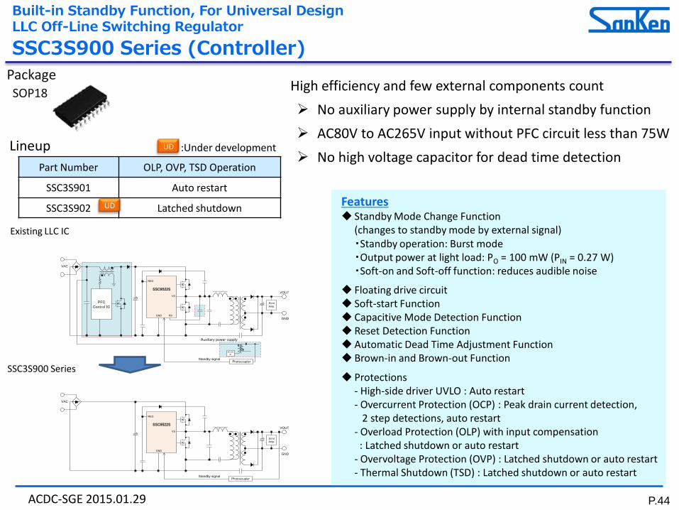
OFF Line LLC ControllerBack to contents
For High power application : industrial equipment etc. Low noise Depending on the application, two types of IC are prepared
*See the Selection Guide of Diode about peripheral diodes.
Type 1: External auxiliary power supply
For Low no-load power consumption (PIN≦30mW)
Type 2: Internal standby function
For low component count
SSC9522S → P.42 SSC3S900→P.44
Bootstrap diode
PWM IC → P.9
AC/DC conv.
(LLC IC)
Standby signal
AC/DC conv.
for standby
PFC
PFC IC→P.48
Bootstrap diode
AC/DC conv.
(LLC IC)
Standby Signal
PFC
PFC IC→P.48

P.42ACDC-SGE 2015.01.29
PackageSOP18
The product achieves high efficiency and few external components count
Capacitive Mode Detection Function:Improving the ability of transformer output power
Automatic Dead Time Adjustment Function
VCC=35V(max.):Flexible transformer design when VCC is supplied by auxiliary power supply
LLC Off-Line Switching Regulator
SSC9522S (Controller)
Features
Floating drive circuit
Soft-start Function
Capacitive Mode Detection Function
Automatic Dead Time Adjustment Function
Brown-in and Brown-out Function
Protections- High-side driver UVLO : Auto restart- Overcurrent Protection (OCP): Peak drain current detection, 2 step detections, auto restart- Overload Protection (OLP): Auto restart - Overvoltage Protection (OVP): Auto restart- Thermal Shutdown (TSD): Auto restart
Characteristic Value
VCC Pin Maximum Ratings 35V
VCC(ON) 11.8V (typ.)
VCC(OFF) 9.8V (typ.)
Minimum Oscillation Frequency 28.3kHz (typ.)
Maximum Oscillation Frequency 300kHz (typ.)
Maximum Source Current -515mA (typ.)
Maximum Sink Current 685mA (typ.)
Electrical characteristics

P.43ACDC-SGE 2015.01.29
Pin assignment
Typical application circuit
No. Symbol Functions No. Symbol Functions
1 VSEN AC input voltage detection signal input 10 COM Ground for power part
2 VCCSupply voltage input for control part, and Overvoltage Protection signal input
11 VGL Low-side gate drive output
3 FBFeedback signal input for constant voltage controland input of Overload Protection signal
12 (NC) −
4 GND Ground for control part 13 (NC) −
5 CSS Soft start capacitor connection 14 VB Supply voltage input for high-side driver
6 OC Overcurrent Protection signal input 15 VS Floating ground for high-side driver
7 RC Resonant current detection signal input 16 VGH High-side gate drive output
8 REG Power supply output for high-side gate drive 17 (NC) −
9 RV Resonant voltage detection signal input 18 (NC) −
LLC Off-Line Switching Regulator
SSC9522S (Controller)
VAC
C1
T1
PC1
D1
RC
R4
R5
R6
R7
R1 R2R11 ROCP
R9D2
D3C11
Cv
Ci
C12
D4
D5
C9
C10
CVCC
C7 C6 C8 C13 C14
C15
C16
PC1
External power supply
VS
VGL
VGH
COMOC
VB
REG
VCC
CSSFB
GND
VSEN
SSC9522S
15
11
2
4
3 5 6 7
10
16
1
8
14
RC
RA(H)
DS(H)RB(H)
RGS(H)
RA(L)
DS(L)RB(L)
RGS(L)
Q(H)
Q(L)
RV9
Crv
U1
P.44ACDC-SGE 2015.01.29
PackageSOP18
High efficiency and few external components count
No auxiliary power supply by internal standby function
AC80V to AC265V input without PFC circuit less than 75W
No high voltage capacitor for dead time detection
Features Standby Mode Change Function
(changes to standby mode by external signal)・Standby operation: Burst mode・Output power at light load: PO = 100 mW (PIN = 0.27 W)・Soft-on and Soft-off function: reduces audible noise
Floating drive circuit Soft-start Function Capacitive Mode Detection Function Reset Detection Function Automatic Dead Time Adjustment Function Brown-in and Brown-out Function
Protections- High-side driver UVLO : Auto restart- Overcurrent Protection (OCP) : Peak drain current detection,
2 step detections, auto restart- Overload Protection (OLP) with input compensation : Latched shutdown or auto restart
- Overvoltage Protection (OVP) : Latched shutdown or auto restart - Thermal Shutdown (TSD) : Latched shutdown or auto restart
SSC3S900 Series
Existing LLC IC
SSC3S900 Series (Controller)
Built-in Standby Function, For Universal DesignLLC Off-Line Switching Regulator
Part Number OLP, OVP, TSD Operation
SSC3S901 Auto restart
SSC3S902 Latched shutdown
Lineup :Under developmentUD
UD
VAC
VOUT
GND
Error
Amp.
SSC9522S
GND
REG
VS
RV
PFCControl IC
PhotocouplerStandby signal
AC/DC IC
Auxiliary power supply
VAC
VOUT
GND
Error
Amp.
SSC9522S
GND
REG
VS
PhotocouplerStandby signal

P.45ACDC-SGE 2015.01.29
VAC
VSPL
VSEN
VCC
FB
ST
NC
VGH
VS
VB
NC
REG
CSS
CL
PL VGL
GND
RC
SB
Standby
VOUT2
GND
VOUT1
T1
PC1 PC2
PC1
PC2
1
15
16
17
18
4
3
2
U1
SS
C3S
900
7
6
5
12
13
14
9
8
10
11
Pin assignment No. Symbol Functions No. Symbol Functions
1 VSEN The mains input voltage detection signal input 10 GND Ground
2 VCCSupply voltage input for the IC, and Overvoltage Protection signal input
11 VGL Low-side gate drive output
3 FB Feedback signal input for constant voltage control 12 REG Supply voltage output for gate drive circuit
4 VSPLThe input voltage detection signal input for OLP Input Voltage Compensation
13 (NC) −
5 CSS Soft-start capacitor connection 14 VB Supply voltage input for high-side driver
6 CL OLP Input Voltage Compensation capacitor connection 15 VS Floating ground for high-side driver
7 RCResonant current detection signal input, and Overcurrent Protection signal input
16 VGH High-side gate drive output
8 PLResonant current detection signal input for OLP Input Voltage Compensation
17 (NC) −
9 SB Standby mode change signal input 18 ST Startup current input
SSC3S900 Series (Controller)
Built-in Standby Function, For Universal DesignLLC Off-Line Switching Regulator
Characteristic Value
VCC Pin Maximum Ratings 35V
VCC(ON) 14V (typ.)
VCC(OFF) 8.9V (typ.)
Minimum Oscillation Frequency 32kHz (typ.)
Maximum Oscillation Frequency 300kHz (typ.)
Maximum Source Current -540mA (typ.)
Maximum Sink Current 1.5A (typ.)
Electrical characteristicsTypical application circuit
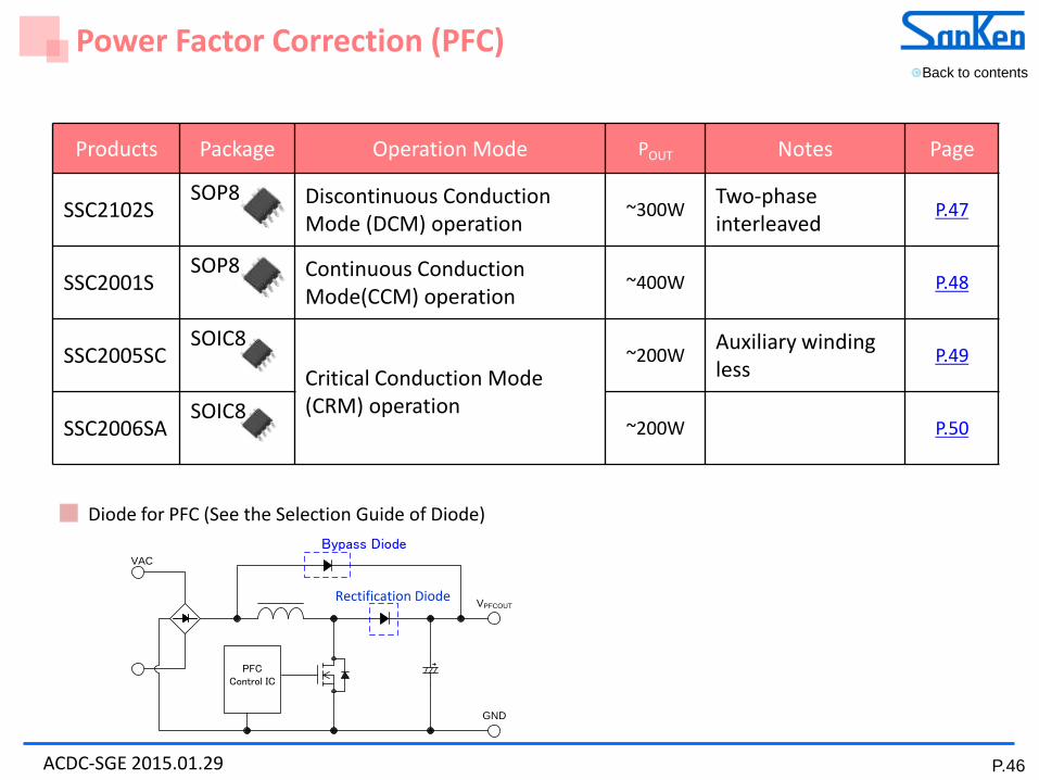
P.46ACDC-SGE 2015.01.29
VAC
VPFCOUT
GND
PFCControl IC
Rectification Diode
Bypass Diode
Products Package Operation Mode POUT Notes Page
SSC2102SSOP8 Discontinuous Conduction
Mode (DCM) operation ~300W
Two-phase interleaved
P.47
SSC2001SSOP8 Continuous Conduction
Mode(CCM) operation ~400W P.48
SSC2005SCSOIC8
Critical Conduction Mode (CRM) operation
~200WAuxiliary winding less
P.49
SSC2006SASOIC8
~200W P.50
Power Factor Correction (PFC)Back to contents
Diode for PFC (See the Selection Guide of Diode)

P.47ACDC-SGE 2015.01.29
Part Number VCC(ON)Maximum On-time
VFB(REF)
SSC2102S 11.6V 20.7µs 3.5V
Discontinuous Conduction Mode (DCM) 2 phase interleaved achieves
Low peak current, low ripple current and low noise Maximum On-time: 15 μs / 20.7 μs (Typ.)
CircuitPin No. Symbol Functions
1 COMP Error amplifier output
2 VIN Rectified input voltage detection
3 VFB Feedback control
4 VCC Power supply for IC
5 OUT2 2nd Gate driver output
6 GND Ground
7 OUT1 1st Gate driver output
8 IS Peak current detection signal input
Pin assignment
FeaturesDiscontinuous Conduction Mode (DCM) 2 phase interleaved Voltage mode control Soft Start Function High Speed Response (HSR)
Protections- Soft Overvoltage Protection (SOVP) : Output voltage decrease- Output Overvoltage Protection (OVP) : Pulse by pulse- Overcurrent Protection (OCP):Dual level OCP, Auto restart- Output Open Loop Detection (OLD) : Switching operation stop and transition to standby mode- Open Terminal Protection (OTP) : Shift to standby mode, auto restart.- Thermal Shutdown (TSD) with hysteresis : Auto restart
SSC2102SPower Factor Correction (PFC) IC of Interleaved DCM Operation
PackageSOP8

P.48ACDC-SGE 2015.01.29
Continuous Conduction Mode (CCM) Low peak current Maximum ON duty is 94 % (Typ.) Error amplifier reference voltage is 3.5 V (Typ.) Brown-in and Brown-out Function
Circuit
D1
R8
R9
C1
L1
D2
R1
8 GATE
7 VCC
1 GND
2 ICOMP
3 IS
4 VINS 5 VCOMP
6 VFB
C8
C3C4
R3
R4
C5 C6
R5 C7
R6
R7
R2
Q1C2
GND
ZD1
外部電源
VACVOUT入力
フィルター
IN
Z1
SSC2001S
E
Part Number VCC(ON) fOSCMaximum On-time
VFB(REF)
SSC2001S 11.3V 65kHz 94% 3.5V
SSC2001S Power Factor Correction (PFC) IC of CCM Operation
Features Continuous Conduction Mode (CCM) Average current control method PWM control (Random Switching Function)High Speed Response (HSR) Brown-in and Brown-out Function
Protections- Overcurrent Protection (OCP) : Auto Restart
Input Current Limitation (OCPL)Peak Current Limitation (OCPH)
- OVP : Pulse by pulse- Output Open Loop Detection (OLD) : Auto restart
Pin No. Symbol Functions
1 GND Ground
2 ICOMP Current amplifier output
3 IS Over current detection signal input
4 VINS Low VIN detection signal input
5 VCOMP Error amplifier out put
6 VFB Feedback control
7 VCC Power supply for IC
8 GATE Gate driver output
Pin assignment
PackageSOP8

P.49ACDC-SGE 2015.01.29
PackageSOIC8
Critical Conduction Mode (CRM) For up to 200 W Application Inductor Current Detection
(No auxiliary winding required) Low Standby Power
(No input voltage sensing required) High accuracy current sensing is -0.60 V±5 %
Features Critical Conduction Mode (CRM) Inductor Current Detection (No auxiliary winding required) Low Standby Power (No input voltage sensing required)Minimum Off-time Limitation Function to restrict the rise of
operation frequencyHigh accuracy overcurrent detection is −0.60 V ± 5 %
Protections- Overcurrent Protection (OCP) : Pulse by pulse- Overvoltage Protection (OVP) : Auto restart- FB pin under voltage protection (FB_ULP) : Auto restart- Thermal Shutdown (TSD) with Hysteresis: Auto restart
CircuitPin No. Symbol Functions
1 FB Feedback, OVP and UVLO signal input
2 COMP Phase compensation
3 RT Maximum on-time adjustment
4 RDLY Turn-on delay time adjustment
5 CS OCP and ZCD signal input
6 GND Ground
7 OUT Gate drive output
8 VCC Power supply input for control circuit
SSC2005SC Power Factor Correction (PFC) IC of CRM Operation
Part Number
VCC(ON) VFB(REF)IOUT
SourceIOUT
Sink
SSC2005SC 12.0 V 2.50 V −500 mA 1000 mA
VAC
C1
BR1 L1
C2
RVS2
VOUT
VCC
OUT COMP
NC
FB
RDLY
GND
CS
8
7
6
5
SSC2005SC
U1
1
2
4
3RT
CS
CPRS
Cf
External Power supply
RT
RDLY
C3
C4
C5
C6
Q1
D1
DBYP
D2
DZCS
R2
R1 R3
RCS
R4
LINE GND
RVS1
Pin assignment

P.50ACDC-SGE 2015.01.29
SSC2006SA Power Factor Correction (PFC) IC of CRM Operation
Part Number
VCC(ON) VFB(REF)IOUT
SourceIOUT
Sink
SSC2006SA 12.0 V 2.50 V −500 mA 1000 mA
Critical Conduction Mode (CRM) For PFC circuit up to 200 W of output power Low standby power
(No input voltage sensing required)
Features Critical Conduction Mode (CRM) Low standby power (No input voltage sensing required)Maximum On-time Limiting Function Restart Function
Protections- Overcurrent Protection (OCP) : Pulse by pulse- Overvoltage Protection (OVP) : Auto restart- FB Pin Undervoltage Protection (FB_UVP) : Auto restart- Thermal Shutdown (TSD): Auto restart
Pin No. Symbol Functions
1 FB Feedback, OVP and UVLO signal input
2 RT Maximum on-time adjustment
3 COMP Phase compensation
4 CS Overcurrent protection signal input
5 ZCD ZCD signal input and delay time adjustment
6 GND Ground
7 OUT Gate drive output
8 VCC Power supply input for control circuit
Pin assignment
Circuit
VAC
C1
BR1P
C2
RVS2
VOUT
VCC
OUT RT
NC
FB
CS
GND
ZCD
8
7
6
5
SSC2006SA
U1
1
2
4
3COMP
CSCP
RS
C7
External power supply RRT
R5
C4
C5
C6
C3
Q1
DFW
DBYP
R2
R3 R4
LINE GND
RVS1
RCS
D
D1T1
R1
TC_SSC2006SA_1_R1
PackageSOIC8

P.51ACDC-SGE 2015.01.29
IMPORTANT NOTES
The contents in this document are subject to changes, for improvement and other purposes, without notice. Make sure that thisis the latest revision of the document before use.
Application examples, operation examples and recommended examples described in this document are quoted for the solepurpose of reference for the use of the products herein and Sanken can assume no responsibility for any infringement ofindustrial property rights, intellectual property rights, life, body, property or any other rights of Sanken or any third party whichmay result from its use.
Unless otherwise agreed in writing by Sanken, Sanken makes no warranties of any kind, whether express or implied, as to theproducts, including product merchantability, and fitness for a particular purpose and special environment, and the information,including its accuracy, usefulness, and reliability, included in this document.
Although Sanken undertakes to enhance the quality and reliability of its products, the occurrence of failure and defect ofsemiconductor products at a certain rate is inevitable. Users of Sanken products are requested to take, at their own risk,preventative measures including safety design of the equipment or systems against any possible injury, death, fires or damages tothe society due to device failure or malfunction.
Sanken products listed in this document are designed and intended for the use as components in general purpose electronicequipment or apparatus (home appliances, office equipment, telecommunication equipment, measuring equipment, etc.).When considering the use of Sanken products in the applications where higher reliability is required (transportation equipmentand its control systems, traffic signal control systems or equipment, fire/crime alarm systems, various safety devices, etc.), andwhenever long life expectancy is required even in general purpose electronic equipment or apparatus, please contact yournearest Sanken sales representative to discuss, prior to the use of the products herein.The use of Sanken products without the written consent of Sanken in the applications where extremely high reliability is required(aerospace equipment, nuclear power control systems, life support systems, etc.) is strictly prohibited.
When using the products specified herein by either (i) combining other products or materials therewith or (ii) physically,chemically or otherwise processing or treating the products, please duly consider all possible risks that may result from all suchuses in advance and proceed therewith at your own responsibility.
Anti radioactive ray design is not considered for the products listed herein.
Sanken assumes no responsibility for any troubles, such as dropping products caused during transportation out of Sanken’sdistribution network.
The contents in this document must not be transcribed or copied without Sanken’s written consent.

DISTRIBUTOR
www.profusionplc.com
Southend-on-SeaEssexSS2 6UNUnited Kingdom
+44 (0)1702 [email protected]