Growth and characterization of 7,7,8,8-tetracyano ... · 1 Growth and characterization of...
12
1 Growth and characterization of 7,7,8,8-tetracyano-quinodimethane crystals on chemical vapor deposition graphene Andrés Black 1,2,ba , Fernando Jiménez 1 , Ramón Bernardo-Gavito 1,b , Santiago Casado 1 , Daniel Granados 1 , Amadeo L. Vázquez de Parga 1,2 1 IMDEA Nanociencia, Calle Faraday 9, Cantoblanco 28049, Madrid, Spain 2 Departamento de Física de la Materia Condensada, Universidad Autónoma de Madrid, Cantoblanco 28049, Madrid, Spain Chemical functionalization of graphene could pave the way for favorably modifying its already remarkable properties. Organic molecules have been utilized to this end as a way to alter graphene’s structural, chemical, electrical, optical and even magnetic properties. One such promising organic molecule is 7,7,8,8-tetracyano-quinodimethane (TCNQ), a strong electron acceptor which has been shown to be an effective p-dopant of graphene. This study explores the thermal evaporation of TCNQ onto graphene transferred onto SiO2/Si substrates. Using two different home-made thermal evaporators, a wide range of TCNQ growth regimes are explored, from thin films to bulk crystals. The resulting graphene/TCNQ structure is characterized via optical microscopy, Raman spectroscopy and atomic force microscopy (AFM). Films are found to be comprised of TCNQ and the oxidized product of TCNQ, α,α-dicyano-p-toluoylcyanide (DCTC), which confirms the electron charge transfer from graphene to the TCNQ films. AFM measurements of these films show that after forming a rather smooth layer covering the graphene surface, small clusters start to form. For higher TCNQ coverage, the clusters agglomerate, becoming quite large in size and forming ripples or wrinkles across the surface. Keywords: A1. Diffusion, A1. Nanostructures, A3. Physical vapor deposition processes, B1. Organic compounds I. INTRODUCTION In the past decade extensive work has been carried out towards the goal of chemically functionalizing graphene to enhance and complement its remarkable properties 1 . Organic molecules have been used to chemically functionalize through both covalent 2 and non-covalent means 3 . TCNQ is an organic molecule that has been successfully used to non-covalently functionalize graphene. A strong electron acceptor, TCNQ has been utilized to produce highly p-doped graphene, resulting in the opening of an electrical bandgap in bilayer graphene 4 , and for use as a conductive anode in graphene organic solar cells 5 . Recent studies carried out in ultra-high vacuum have found that TCNQ deposited onto graphene grown epitaxially on ruthenium is able to form extended spin-split electronic bands resulting in long range magnetic order 3 . X-ray photoemission spectroscopy (XPS) and scanning tunneling microscopy (STM) measurements confirmed that charge transfer from the ruthenium substrate to the TCNQ, modulated by the graphene layer in between, caused the molecules to develop a magnetic moment 6,7 . TCNQ and its salts have been studied extensively by Raman spectroscopy, confirming their strong electron accepting capabilities for both films and crystals synthesized by evaporation or a Author to whom correspondence should be addressed: [email protected] b Currently Physics Department, Lancaster University, LA1 4YB, Lancaster, United Kingdom
Transcript of Growth and characterization of 7,7,8,8-tetracyano ... · 1 Growth and characterization of...

1
Growth and characterization of 7,7,8,8-tetracyano-quinodimethane crystals
on chemical vapor deposition graphene
Andrés Black1,2,ba, Fernando Jiménez1, Ramón Bernardo-Gavito1,b, Santiago
Casado1, Daniel Granados1, Amadeo L. Vázquez de Parga1,2
1IMDEA Nanociencia, Calle Faraday 9, Cantoblanco 28049, Madrid, Spain
2Departamento de Física de la Materia Condensada, Universidad Autónoma de Madrid, Cantoblanco
28049, Madrid, Spain
Chemical functionalization of graphene could pave the way for favorably modifying its already
remarkable properties. Organic molecules have been utilized to this end as a way to alter
graphene’s structural, chemical, electrical, optical and even magnetic properties. One such
promising organic molecule is 7,7,8,8-tetracyano-quinodimethane (TCNQ), a strong electron
acceptor which has been shown to be an effective p-dopant of graphene. This study explores
the thermal evaporation of TCNQ onto graphene transferred onto SiO2/Si substrates. Using two
different home-made thermal evaporators, a wide range of TCNQ growth regimes are explored,
from thin films to bulk crystals. The resulting graphene/TCNQ structure is characterized via
optical microscopy, Raman spectroscopy and atomic force microscopy (AFM). Films are found
to be comprised of TCNQ and the oxidized product of TCNQ, α,α-dicyano-p-toluoylcyanide
(DCTC), which confirms the electron charge transfer from graphene to the TCNQ films. AFM
measurements of these films show that after forming a rather smooth layer covering the
graphene surface, small clusters start to form. For higher TCNQ coverage, the clusters
agglomerate, becoming quite large in size and forming ripples or wrinkles across the surface.
Keywords: A1. Diffusion, A1. Nanostructures, A3. Physical vapor deposition processes, B1.
Organic compounds
I. INTRODUCTION
In the past decade extensive work has been carried out towards the goal of chemically
functionalizing graphene to enhance and complement its remarkable properties1. Organic
molecules have been used to chemically functionalize through both covalent2 and non-covalent
means3. TCNQ is an organic molecule that has been successfully used to non-covalently
functionalize graphene. A strong electron acceptor, TCNQ has been utilized to produce highly
p-doped graphene, resulting in the opening of an electrical bandgap in bilayer graphene4, and
for use as a conductive anode in graphene organic solar cells5. Recent studies carried out in
ultra-high vacuum have found that TCNQ deposited onto graphene grown epitaxially on
ruthenium is able to form extended spin-split electronic bands resulting in long range magnetic
order3. X-ray photoemission spectroscopy (XPS) and scanning tunneling microscopy (STM)
measurements confirmed that charge transfer from the ruthenium substrate to the TCNQ,
modulated by the graphene layer in between, caused the molecules to develop a magnetic
moment6,7.
TCNQ and its salts have been studied extensively by Raman spectroscopy, confirming their
strong electron accepting capabilities for both films and crystals synthesized by evaporation or
a Author to whom correspondence should be addressed: [email protected] b Currently Physics Department, Lancaster University, LA1 4YB, Lancaster, United Kingdom
2
from solution8-13. Depending on the growth conditions and substrate, the oxidation product of
TCNQ2-, α,α-dicyano-p-toluoylcyanide (DCTC) is often detected. For TCNQ films evaporated
onto Ag, DCTC was detected for thin films, suggesting that the layers close to the Ag substrate
were ionized and oxidized. As the TCNQ film thickness increased, DCTC was no longer
detected, suggesting that the upper layers of the film were comprised of neutral TCNQ14.
Similar behavior has been observed via XPS measurements for F4-TCNQ molecules deposited
on epitaxial graphene on SiC. Electron transfer from the graphene to the first few layers of
adsorbed F4-TCNQ was found to p-dope the graphene15. For CVD grown graphene transferred
to an insulating substrate, DCTC was also detected for low coverage, whereas only TCNQ was
detected for higher coverages, suggesting a similar mechanism of electron charge transfer from
the graphene substrate to the first few TCNQ layers adjacent to it16.
This study seeks to understand the growth process and morphology of TCNQ evaporated onto
Chemical Vapor Deposition (CVD) grown graphene transferred onto SiO2/Si substrate, which
is commonly used for device fabrication. Understanding the growth mechanism of TCNQ on
graphene is necessary for the further development of devices based on graphene/TCNQ
structures, with the hope of exploiting the unique properties of each material. TCNQ films have
been shown to be effective graphene dopants as well as exhibiting magnetic properties3,
whereas TCNQ crystals have been shown to have unique electrical17 and optoelectronic18
properties when interfaced with adequate complementary organic crystals. Different growth
regimes of TCNQ on graphene were explored by varying the sublimation temperature,
substrate temperature and vapor concentration of the TCNQ. This resulted in various
TCNQ/graphene structures, ranging from thin films to pure TCNQ crystals. Electron charge
transfer from the graphene to the TCNQ and subsequent oxidation to DCTC, as previously seen
by Qi et al16, was confirmed for thin films via Raman spectroscopy. Atomic force microscopy
measurements (AFM) showed that at low coverage, the TCNQ films seems to have almost no
effect on the graphene surface, whereas for increasing coverage, clusters form, growing in size
to the point that they strain the graphene and form filament-like wrinkles.
II. METHODS
Graphene was grown on 25 µm thick polycrystalline copper foil via chemical vapor deposition
in a CVD furnace. The foil was heated to 1000° C while flowing 100 standard cubic centimeters
(sccm) hydrogen. The temperature was allowed to stabilize for 10 minutes, before increasing
the hydrogen flow to 500 sccm and introducing 1 sccm methane for 25 minutes in order to
induce graphene growth. The furnace was then rapidly cooled to room temperature while
flowing 100 sccm hydrogen. The entire process was carried out at 10 mbar. Graphene was then
transferred to a highly n-doped silicon substrate terminated with a 300 nm SiO2 layer. To
achieve the transfer, a PMMA layer was spun on the copper foil (about 180 nm thickness),
before etching the copper foil in an ammonium persulfate etchant (0.1 g/mL in deionized
water). After rinsing the PMMA/graphene stack several times in deionized water, the stack was
scooped out with the target Si/SiO2 wafer. The graphene was allowed to dry over night before
removing the PMMA layer by rinsing in acetone. Thermal annealing was then carried out at
300° C in Ar/H2 96/4% in order to remove remaining PMMA residues. Raman spectroscopy
measurements were carried out using a 488 nm laser, with a spot size of about 1 μm using an
x80 objective and collected in a cooled silicon CCD detector (Andor Newton), with a 0.5 m
spectrometer length and a 300 l/mm grating.

3
Figure 1 Picture of large tube TCNQ evaporator with aluminum foil removed from exterior.
Samples are placed at the tube mouth and inside the tube, 2 cm away from tube bottom. In the
small tube evaporator, the sample is placed only on the mouth of the tube.
TCNQ evaporation was carried out in a quartz tube placed inside a vacuum desiccator, at a
pressure of 600 mbar. For each growth one of two quartz tubes were used, a small one (3.5 cm
long, 1.8 cm diameter) or a large one (8 cm long, 2.3 cm diameter), shown in Figure 1. The
lower region of both quartz tubes were heated resistively, by coiling tungsten wire around the
exterior of the tubes. 100 mg TCNQ powder (Sigma Aldrich 157635) was placed inside the
bottom of the tube. In order to achieve more homogeneous heating, aluminum foil was also
wrapped around the bottom 2 cm of the tubes. An in situ thermocouple was used to calibrate
the relation between the power dissipated in the resistive coil (usually between 2 and 10 W)
and the temperature at the bottom of the tube, and subsequent evaporations were carried out
without the thermocouple. The quartz tubes were sealed at their mouth openings with a glass
slide, with the graphene/SiO2 samples mounted on the glass slide facing the TCNQ powder
inside the tube. In the case of the large evaporator, apart from at the tube mouth, samples were
also mounted inside the quartz tube 2 cm away from the tube bottom, facing the TCNQ powder,
as shown in Figure 1.
III. RESULTS AND DISCUSSION
Figure 2 shows white light reflection optical images of TCNQ evaporated onto graphene/SiO2
for different sublimation temperatures and growth times in the small tube evaporator. As seen
in Figure 2(a), a growth temperature of 130° C for 75 minutes results in the formation of pellet-
like crystals on the surface of the graphene, with lateral dimensions on the order of 5 µm. These
crystals are separated by a typical distance of a few dozen microns, indicating the high mobility
of the individual TCNQ molecules on graphene. Increasing the growth temperature to 160° C
and maintaining the same growth time clearly changes the growth regime, as shown in Figure
2(b). The graphene substrate is no longer visible and seems to have been covered by a thick
film. The morphology of the crystals on the surface has also changed, from pellets to needles
with a typical length on the order of 10 µm. The needles are packed more closely together on
the surface than the pellets, with many needles touching each other. It seems that the rise in the
sublimation temperature substantially modifies the density of TCNQ molecules on the surface.
Now the molecules are no longer able to reach the initial condensation points, on the contrary
the TCNQ molecules self-assemble, probably via H-bonds3, forming a full layer that reduces
the effective diffusion length of the incoming molecules and as consequence increases the
density of 3D islands. From this temperature the growth mode remains unchanged and further
increasing the growth temperature to 180° C completely saturates the graphene surface with

4
TCNQ needles, as shown in Figure 2(c), despite a reduction in the evaporation time from 75 to
45 minutes. Evaporating at the highest temperature obtainable in the small tube evaporator,
200° C, for 45 minutes, maintains the high crystal density on the surface but results in a change
in the structure of the crystals, as seen in Figure 2(d). Apart from needles, many plaque-shaped
crystals are seen on the surface, with a typical size of 5 to 10 µm.
Figure 2 Optical images of TCNQ evaporated onto graphene/SiO2/Si substrate in small tube
evaporator with the following conditions: (a) 75 minutes at 130° C, (b) 75 minutes at 160° C,
(c) 45 minutes at 180° C and (d) 45 minutes at 200°. All scale bars 25 µm.
The large tube evaporator (diameter 2.3 cm and length 8 cm) can accommodate two samples
simultaneously, one at the extreme of the tube, where the sample remains close to room
temperature, and another one inside the tube close to the resistive heating coils, where the
sample is heated along with the TCNQ powder. This configuration allows for the comparison
of the TCNQ film growth at different substrate temperatures for the same evaporation run.
Figure 3 shows optical images of TCNQ evaporated onto graphene/SiO2 for different growth
conditions in the large tube evaporator. Figure 3(a), (b) show the images corresponding to the
substrate placed at the mouth of the tube, where it remains close to room temperature.
Evaporating at 120° C for 60 minutes results in the formation of TCNQ crystal pellets, as seen
in Figure 3(a). Figure 3(b) shows that increasing the growth temperature to 170° C favors the
formation of short needles on the graphene surface, with a typical length of 2 to 3 µm, in a very
dense configuration, with most needles touching another needle. The comparison with images
shown in Figure 2(a), (b) reveals a similar morphology for both growth conditions. When the
substrate remains close to room temperature, the main findings can summarized as follows: for
lower sublimation temperatures the growth of pellet-like TCNQ crystals occurs, whereas for

5
higher sublimation temperatures, the growth regime changes, with the TCNQ molecules on the
surface forming needles that are closer to each other than the pellets.
Figure 3 Optical images of TCNQ evaporated onto graphene/SiO2/Si substrate in large tube
evaporator with the conditions outlined on the margins of the images. Scale bar in (c) is 40 µm,
(a), (b) and (d) are 15 µm. Inset: Same sample as in a, showing the boundary between graphene
(left) and bare SiO2 (right). TCNQ crystals can be seen on both sides of the boundary. Scale bar
250 µm.
It is worth noting that the samples obtained for the evaporation done in the small tube and in
the large tube with the substrate place at the mouth present differences in the crystal coverages
obtained, despite similar growth conditions and substrate temperatures. The main difference is
the higher crystal coverage obtained with the small tube compared to substrates on the mouth
of the large tube. The reason for this behavior is not completely clear, since the vapor pressure
and hence concentration of TCNQ molecules at the same evaporation temperature should be
equal regardless of the tube size. One possible reason for the different crystal coverage is that
the TCNQ molecules have more surface area upon which they can be deposited in the large
tube. If a larger proportion of the TCNQ molecules are sticking to the tube walls in the large
tube, then fewer TCNQ molecules will end up reaching the substrate at the mouth of the tube,
despite the fact that the theoretical TCNQ vapor pressure is the same at a given temperature.
In addition, the substrate in the small tube is fairly close to the heat source and may be heated
slightly above ambient, whereas the substrate at the mouth of the large tube is far from the heat
source and therefore remains at ambient temperature. This difference in substrate temperature
could be an additional factor in explaining the differences in growth regime.

6
For samples placed on the inside of the large tube, where the substrate is heated during the
evaporation, no TCNQ crystals were formed for any of the growth conditions, only TCNQ
films. For low TCNQ coverage, like that shown in Figure 3(c), practically no changes are
noticeable on the graphene surface when compared to pristine graphene. By increasing the
evaporation temperature from 120° C to 170° C, a change is observed in the coloration of the
graphene, which becomes slightly bluer as seen in Figure 3(d) (note that in all of these images,
the white balance has been adjusted to make bare SiO2 background equal). More interestingly,
blue patches and spots are visible amongst the purple background, covering almost half of the
surface area and with a typical size of 15 to 20 µm.
From these results it is clear that the growth mechanism on both the large and small tube
evaporator is the same for the substrates held close to room temperature, and leads to the
formation of TCNQ crystals. When the substrate is held at elevated temperatures during
evaporation the TCNQ deposition produces a uniform thin molecular film on the graphene
substrate. This change in the structure of the resulting sample may be due to two different
mechanisms. Firstly, an elevated substrate temperature increases desorption, reducing the
overall sticking coefficient of the TCNQ molecules present on the graphene surface. Secondly,
TCNQ molecules on the elevated temperature substrate will have more thermal energy to
diffuse about the surface, making it less likely they will remain stuck to previously formed
TCNQ clusters they encounter, thereby limiting the formation of large crystals. Desorption of
the TCNQ molecules from the substrates held at high temperature during the growth can be
checked by evaporating TCNQ molecules on bare SiO2 surface. On this surface, a shorter
diffusion length is expected in comparison to graphene. For growths with the substrate at high
temperatures, no TCNQ is detected on the SiO2 surface, either via optical inspection or Raman
spectroscopy, indicating that the sticking coefficient for TCNQ on SiO2 at elevated
temperatures drops to zero. At low substrate temperatures, however, TCNQ crystals form on
the SiO2 surface in much the same way as they do on the graphene surface, as can be seen by
the inset in Figure 3(a). For both graphene and SiO2 surfaces, the TCNQ sticking coefficient
is high for low substrate temperatures and low for high substrate temperatures.
Raman spectroscopy measurements were carried out of the TCNQ/graphene structures, with
spectra from growths in the small tube shown in Figure 4(a), and spectra from the films grown
on the inside of the large tube shown in Figure 4(b). A reference spectrum of pristine graphene
on SiO2 is also shown in Figure 4(a), exhibiting the typical 2D peak near 2700 cm-1 and G peak
near 1585 cm-1. The very low intensity of the D peak, located near 1350 cm-1 and associated
with disorder in the graphene lattice, confirms the low density of defects in graphene, while
the large ratio between the intensities of the 2D and G peaks confirms that the graphene is
monolayer19. The red curve in Figure 4(a) was taken between the crystals on the surface of the
sample from Figure 2(a). This spectrum continues to show the graphene 2D and G peaks, but
with a diminished intensity in the ratio between the two peaks compared to the pristine
graphene spectrum. The peaks observed at 1179, 1288 and 1621 cm-1 are associated with the
presence of DCTC, the oxidation product of TCNQ, replicating the measurements made in Qi
et al16. In addition to the DCTC, the presence of TCNQ on the graphene surface is confirmed
from the peaks at 1204, 1446, and 2218 cm-1 8,12,9. The peak located at 1592 cm-1 results from
a combination of the graphene G peak and a TCNQ peak at 1598 cm-1. An increase in the
graphene D peak is also observed, suggesting that the graphene is more disordered after the
TCNQ evaporation. The presence of both TCNQ and DCTC on the surface in between crystal
pellets confirms that electron charge transfer between the graphene and the TCNQ molecules
is occurring. The blue curve in Figure 4(a) also shows Raman spectra taken on top of the

7
crystals from Figure 2(a) (blue curve). Strong, pure TCNQ peaks are detected, with no sign of
graphene or DCTC, with identical results obtained whenever Raman spectra were taken on top
of needle or pellet-like crystals.
Figure 4 Raman spectra of pristine graphene on SiO2, as well as TCNQ evaporated onto
graphene with different conditions in (a) mouth of small tube evaporator and (b) inside of large
tube evaporator.
The information gathered from the optical image in Figure 2(a) and the corresponding Raman
spectra between and on top of the crystals would suggest that as a TCNQ/DCTC film forms on
the graphene surface, microscopic clusters of TCNQ crystals are created and grow to become
ever larger TCNQ crystals. It is possible that defects, rips, tears or foreign impurities on the
graphene surface act as heterogeneous nucleation sites for the formation of the TCNQ clusters.
These TCNQ clusters grow into crystals by incorporating TCNQ molecules both directly from
the atmosphere and from diffusing TCNQ molecules on the substrate surface, which become
absorbed into the TCNQ crystals when they come into contact with it. As evaporation
temperatures are increased, an increase in the nucleation density of the TCNQ crystals is
observed, as well as a saturation of the graphene surface with a thick TCNQ film. Additionally,
instead of forming pellets, the formation of needle-like TCNQ crystals is favored, as has been
observed in the vapor growth of other organic crystals20,21.
Raman spectra taken of samples grown on the inside of the large tube, where the substrate is
heated during growth, shown in Figure 4b, detect the presence of TCNQ and DCTC covering
the entire surface for evaporation temperatures as low as 85° C. At this low temperature (red

8
curve in Figure 4(b)), the graphene peaks are quite strong, and weak peaks corresponding
mostly to DCTC are identifiable in the range between 1150 and 1300 cm-1, as well as a TCNQ
peak at 2220 cm-1. A slight increase in the graphene D peak is also observed. Increasing the
evaporation temperature to 120° C, corresponding to the sample shown in Figure 3(c),
intensifies both TCNQ and DCTC peaks with respect to the graphene peaks, although an
increase in the D peak is also appreciable. For the highest achievable evaporation temperature
in the large tube evaporator, 170° C, corresponding to the sample shown in Figure 3(d), only
TCNQ peaks are detectable, along with a weakened graphene 2D peak, with no sign of DCTC.
It would seem that for these high coverages, the bulk TCNQ film is thick enough that it
overwhelms any signal that may be coming from the oxidized layers of DCTC adjacent to the
graphene, where charge transfer is occurring. The measured G peak frequency is seen to
increase from around 1585 cm-1 in pristine graphene towards 1600 cm-1 for samples grown in
both the large and small evaporator. This is another indication that there is charge transfer from
the graphene to the TCNQ molecules, resulting in graphene p-doping22,23. Apart from the
charge transfer, part of this apparent shift in the graphene G peak may also be due to its merging
with the TCNQ peak situated at 1600 cm-1.
In order to clarify the structure of the graphene/TCNQ films, and what might be causing the
slight increase in the graphene D peak upon TCNQ evaporation, AFM measurements were
carried out of the TCNQ films grown with the substrate at elevated temperatures. The resulting
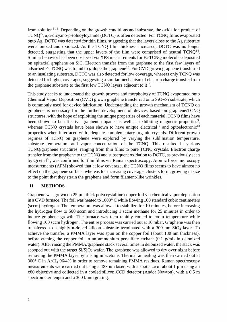
images are shown in Figure 5. A pristine graphene surface, after thermal annealing to remove
PMMA residues, is shown in Figure 5(a). Some folds are visible along the graphene, with a
typical height between 2 and 3 nm. A few much larger PMMA clusters remain on the film,
with heights varying between 20 and 30 nm, although the surface is mostly clean. The RMS
value of the region outlined by the blue 1.5 by 1.5 µm square shown in the figure is 0.73 nm.
For evaporation at low temperatures (between 85° C and 110° C) up to 120 minutes, practically
no change was discernible in the surface when compared to pristine graphene. Increasing the
evaporation temperature to 120° C produces an obvious change on the graphene surface, as
seen in Figure 5(b), with the appearance of small TCNQ/DCTC clusters. These clusters seem
to be randomly dispersed about the graphene surface, aggregating in groups with a typical size
of 50 to 200 nm, and heights between 2 and 3 nm. The RMS value of the blue square is 1.1 nm.
9
Figure 5 AFM images of (a) pristine graphene and TCNQ evaporated onto graphene/SiO2
inside the large tube evaporator with the following conditions: (b) 60 minutes at 120° and (c)
120 minutes at 170° C.
Figure 5I shows an AFM image of a sample with a very high TCNQ coverage, with 120 minutes
evaporation at 170° C. From this image it is evident that the surface morphology has changed

10
significantly. Firstly, there are rather large clusters which have agglomerated, with heights
ranging between 10 to 20 nm and typical size of several hundred nm. The RMS of the blue
square has increased to 2.0 nm. In addition, some sort of filament or string-like feature can be
seen to extend from cluster to cluster, with a typical height of 1.5 to 2.5 nm. It is possible that
these filaments are folds or wrinkles on the graphene surface caused by the TCNQ clusters, or
even the intercalation of TCNQ below the graphene surface. Indeed, intercalation of various
atomic elements has been observed to occur in ultra-high vacuum conditions for several
graphene/metallic substrate systems24,25. Defect sites in the graphene lattice are speculated to
serve as the points for the evaporated substance to intercalate between the graphene and the
substrate. A similar mechanism could be at work in this case, with small defects or even larger
rips and tears in the graphene serving as points of entry for the intercalation of TCNQ
molecules. If the observed wrinkles are indeed occurring in the graphene as a result of the
TCNQ evaporation, it would be creating stress on the graphene lattice and possibly increasing
the defect density, explaining the D peak intensity increase observed in Raman measurements.
IV. CONCLUSIONS
TCNQ was thermally evaporated onto CVD grown graphene transferred to Si/SiO2substrates.
High growth temperatures and long growth times readily resulted in the formation of TCNQ
crystals on the graphene surface. For increasing temperatures, the crystals changed from having
a pellet shape and being spaced widely apart on the surface, to densely packed TCNQ needles.
Films were formed on the graphene for low evaporation temperatures, or when the graphene/
SiO2 substrate was heated. Raman spectroscopy confirmed that the graphene films were
comprised of TCNQ and DCTC, the oxidation product of TCNQ, which requires an electron
charge transfer from the substrate to the TCNQ for its formation. For higher TCNQ coverages,
the films only exhibited TCNQ peaks, indicating that the signal from the bulk TCNQ film
overwhelms the signal from first few oxidized layers of DCTC. For very low TCNQ coverage,
AFM measurements barely detected any change in the graphene surface. As coverage
increased, nanometer sized clusters began to form, eventually forming clusters with heights up
to 20 nm and typical sizes of several hundred nanometers. Filament-like ripples were seen to
form between the clusters, which we speculate may be wrinkles in the graphene lattice caused
by stress from the clusters, or from TCNQ molecules intercalated beneath the graphene.
ACKNOWLEDGEMENTS
Financial support by the Ministerio de Economía y Competitividad (MINECO) through grants
FIS2013-40667-P, FIS2015-67367-C2-1-P and SUPERMNAN (ESP2015-65597-C4-3-R) and
Comunidad de Madrid through the program MAD2D P2013/MIT-3007 is gratefully
acknowledged. D.G. acknowledges RYC-2012-09864, A.B. acknowledges FPI-UAM
program.
REFERENCES
1. V. Georgakilas, M. Otyepka, A. B. Bourlinos, V. Chandra, N. Kim, K. C. Kemp, P.
Hobza, R. Zboril, K. S. Kim. Chemical Reviews 112, 6156-6214 (2012).
2. J. J. Navarro, S. Leret, F. Calleja, D. Stradi, A. Black, R. Bernardo-Gavito, M.
Garnica, D. Granados, A. L. Vázquez de Parga, E. M. Pérez and R. Miranda. Nano
Letters 16, 355-361 (2016).

11
3. M. Garnica, D. Stradi, S. Barja, F. Calleja, C. Díaz, M. Alcamí, N. Martín, A. L.
Vázquez de Parga, F. Martín and R. Miranda. Nature Physics 9, 368-374 (2013).
4. W. Zhang, C.-T. Lin, K.-K. Liu, T. Tite, C.-Y. Su, C.-H. Chang, Y.-H. Lee, C.-W.
Chu, K.-H. Wei, J.-L. Kuo and L.-J. Li. ACS Nano 5, 7517-7524 (2011).
5. C.-L. Hsu, C.-T. Lin, J.-H. Huang, C.-W. Chu, K.-H. Wei and L.-J. Li. ACS Nano 6,
5031-5039 (2012).
6. M. Garnica, D. Stradi, S. Barja, C. Díaz, M. Alcamí, A. Arnau, A. L. Vázquez de
Parga, F. Martín and R. Miranda. Nano Letters 14, 4560-4567 (2014).
7. D. Maccariello, M. Garnica, M. A. Niño, C. Navío, P. Perna, S. Barja, A. L. Vázquez
de Parga, and R. Miranda. Chemistry of Materials 26, 2883–2890 (2014).
8. M. S. Khatale, J. P. Devlin. The Journal of Chemical Physics 70, 1851-1859 (1979).
9. M. Harris, J. J. Hoaglang, U. Mazur and K. W. Hipps. Vibrational Spectroscopy 9,
273-277 (1995).
10. A. Pawlukojć, I. Naktaniec, G. Bator, L. Sobczyk and E. Grech. Chemical Physics
Letters, 378, 665-672 (2003).
11. X. Jiang, Z. Li, C. Sun and X. Zhang. Journal of the Physical Sciences 7, 901-905
(2012).
12. D. L. Jeanmarie and R. P. Van Duyne. Journal of the American Chemical Society 98,
4029-4033 (1976).
13. H.-H. Tseng, M. Serri, N. M. Harrison and S. Heutz. Journal of Materials Chemistry
C 3, 8694 (2015).
14. M. Yoshikawa, S. Nakashima and A. Mitsuishi. Journal of Raman Spectroscopy 17,
369-371 (1986).
15. W. Chen, S. Chen, D. C. Qi, X. Y. Gao and A. T. S. Wee. Journal American
Chemical Society 129, 10418-10422 (2007).
16. Y. Qi, U. Mazur and K. W. Hipps. RSC Advances 2, 10579-10584 (2012).
17. H. Alves, A. S. Molinari, H. Xie and A. Mopurgo. Nature Materials 7, 574-580
(2008).
18. H. Alves, R. M. Pinto and E. S. Maçôas. Nature Communications 4, 1842 (2013).
19. A. C. Ferrari. Solid State Communications 143, 47-57 (2007).
20. D. J. Mascaro, M. E. Thompson, H. I. Smith and V. Bulović. Organic Electronics 6,
211-220 (2005).
21. F. Yang, M. Shtein, and S. R. Forrest. Journal of Applied Physics 98, 014906 (2005).

12
22. A. Das, S. Pisana, B. Chakraborty, S. Piscanec, S.K. Saha, U.V. Waghmare, K.S.
Novoselov, H.R. Krishnamurthy, A.K. Geim, A.C. Ferrari and A.K. Sood. Nature
Nanotechnology 3, 210-215 (2008).
23. K. Sasaki, K. Kato, Y. Tokura, S. Suzuki, T. Sogawa. Physical Review B 86, 201403
(2012).
24. S. Vlaic, A. Kimouche, J. Coraux, B. Santos, A. Locatelli and N. Rougemaille.
Applied Physics Letters 104, 101602 (2014).
25. F. Calleja, H. Ochoa, M. Garnica, S. Barja, J. J. Navarro, A. Black, M. M. Otrokov,
E.V. Chulkov, A. Arnau, A. L. Vázquez de Parga, F. Guinea and R. Miranda. Nature
Physics 11, 43-47 (2015).


![Groundwater Investigation and Characterization · Groundwater Investigation and Characterization ... manual for environmental site characterization [2] ... through drilling, well](https://static.fdocuments.in/doc/165x107/5b4001557f8b9a5e528ccc77/groundwater-investigation-and-characterization-groundwater-investigation-and.jpg)