GPON ONU Triplexer Transceiver - accelink.com · RTXM170-611 GPON ONU Triplexer Transceiver is...
5
RTXM170-611 Wuhan Telecommunication Devices Co., Ltd. http://www.wtd.com.cn 1 GPON ONU Triplexer Transceiver RTXM170-611 Features Single Fiber Triplexer 1.25Gbps data upstream /2.5Gbps data downstream /45~1002MHz CATV analog signal downstream Burst mode transmission with 1310nm DFB laser Continuous mode digital receiver with 1490nm APD-TIA Analog CATV receiver with 1555nm InGaAs PIN detector +3.3V /+12V power supply CML compatible data input CML compatible data output CML transmitter burst-mode control LVTTL I2C DDM interface LVTTL TX_SD and RX_SD Soft Enable/Disable TX and Video Fully RoHS Compliant All metal housing for superior EMI performance Excellent ESD/TVS protection -40℃ to +85℃ operating temperature 1×20 Pin and 2”×2” Package 3PIN RF output connector Real time monitoring of: Temperature Supply voltage Laser bias current Transmitted optical power Received optical power Video Received optical power RF Output level
Transcript of GPON ONU Triplexer Transceiver - accelink.com · RTXM170-611 GPON ONU Triplexer Transceiver is...

RTXM170-611
Wuhan Telecommunication Devices Co., Ltd.http://www.wtd.com.cn
1
GPON ONU Triplexer Transceiver
RTXM170-611
FeaturesSingle Fiber Triplexer1.25Gbps data upstream /2.5Gbpsdata downstream /45~1002MHzCATV analog signal downstreamBurst mode transmission with1310nm DFB laserContinuous mode digital receiverwith 1490nm APD-TIAAnalog CATV receiver with1555nm InGaAs PIN detector+3.3V /+12V power supplyCML compatible data inputCML compatible data outputCML transmitter burst-modecontrolLVTTL I2C DDM interfaceLVTTL TX_SD and RX_SD
Soft Enable/Disable TX and VideoFully RoHS CompliantAll metal housing for superior EMIperformanceExcellent ESD/TVS protection-40℃ to +85℃ operatingtemperature1×20 Pin and 2”×2” Package3PIN RF output connectorReal time monitoring of:
TemperatureSupply voltageLaser bias currentTransmitted optical powerReceived optical powerVideo Received optical powerRF Output level
RTXM170-611
Wuhan Telecommunication Devices Co., Ltd.http://www.wtd.com.cn
2
ApplicationsGPON ONU Side Voice/Data/Video FTTx
StandardsITU-T G.984.2 Class B+ITU-T G.984.5
SFF-8472 Rev 10.2RoHS 6
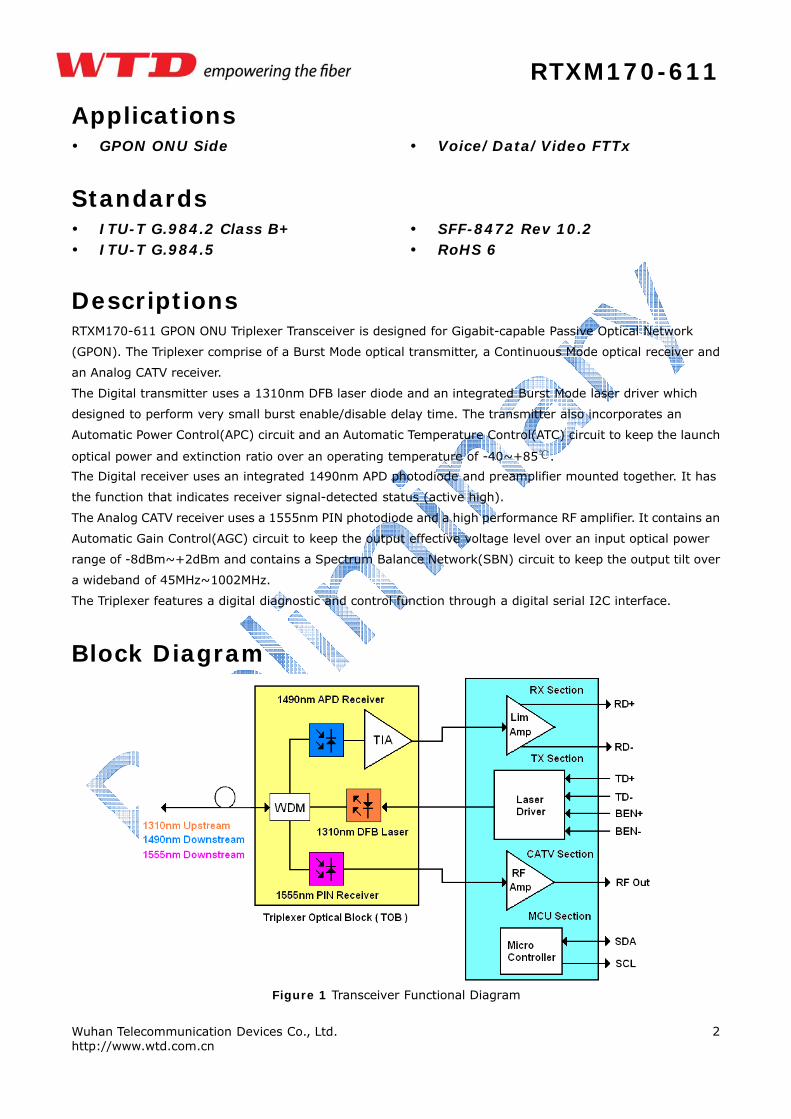
DescriptionsRTXM170-611 GPON ONU Triplexer Transceiver is designed for Gigabit-capable Passive Optical Network
(GPON). The Triplexer comprise of a Burst Mode optical transmitter, a Continuous Mode optical receiver and
an Analog CATV receiver.
The Digital transmitter uses a 1310nm DFB laser diode and an integrated Burst Mode laser driver which
designed to perform very small burst enable/disable delay time. The transmitter also incorporates an
Automatic Power Control(APC) circuit and an Automatic Temperature Control(ATC) circuit to keep the launch
optical power and extinction ratio over an operating temperature of -40~+85℃.
The Digital receiver uses an integrated 1490nm APD photodiode and preamplifier mounted together. It has
the function that indicates receiver signal-detected status (active high).
The Analog CATV receiver uses a 1555nm PIN photodiode and a high performance RF amplifier. It contains an
Automatic Gain Control(AGC) circuit to keep the output effective voltage level over an input optical power
range of -8dBm~+2dBm and contains a Spectrum Balance Network(SBN) circuit to keep the output tilt over
a wideband of 45MHz~1002MHz.
The Triplexer features a digital diagnostic and control function through a digital serial I2C interface.
Block Diagram
Figure 1 Transceiver Functional Diagram
RTXM170-611
Wuhan Telecommunication Devices Co., Ltd.http://www.wtd.com.cn
6
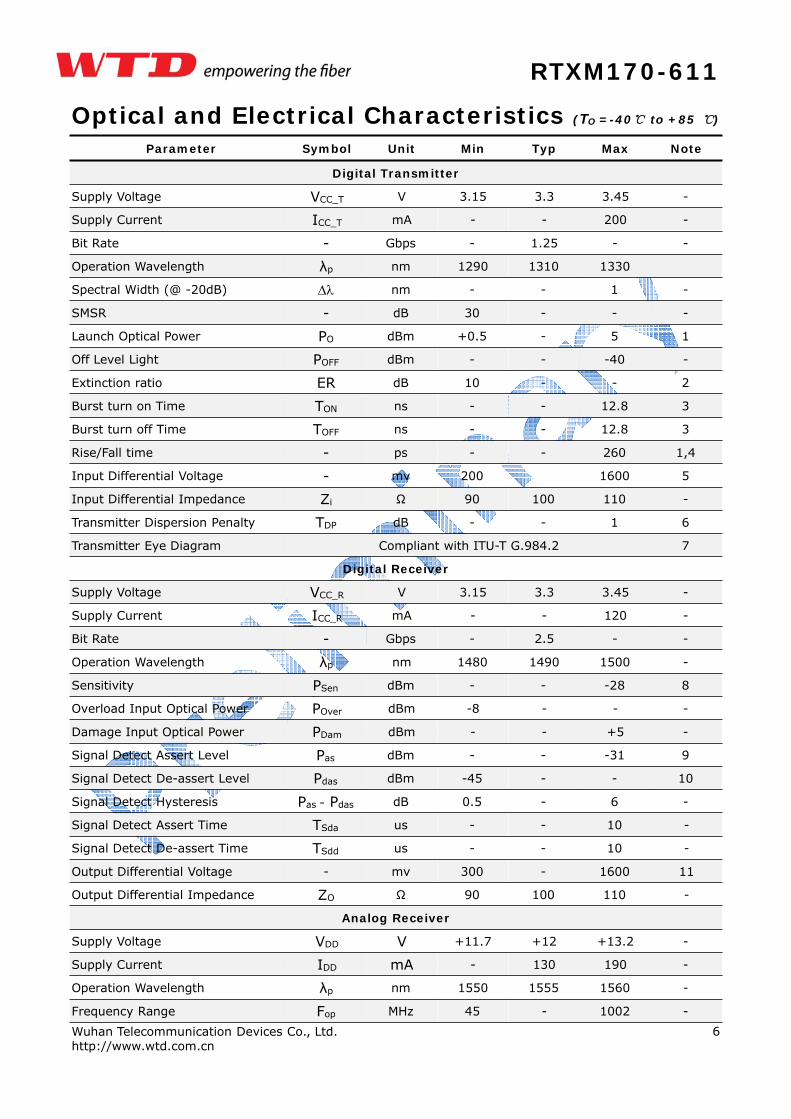
Optical and Electrical Characteristics (TO =-40℃ to +85 ℃)
Parameter Symbol Unit Min Typ Max Note
Digital Transmitter
Supply Voltage VCC_T V 3.15 3.3 3.45 -
Supply Current ICC_T mA - - 200 -
Bit Rate - Gbps - 1.25 - -
Operation Wavelength λp nm 1290 1310 1330
Spectral Width (@ -20dB) Δλ nm - - 1 -
SMSR - dB 30 - - -
Launch Optical Power PO dBm +0.5 - 5 1
Off Level Light POFF dBm - - -40 -
Extinction ratio ER dB 10 - - 2
Burst turn on Time TON ns - - 12.8 3
Burst turn off Time TOFF ns - - 12.8 3
Rise/Fall time - ps - - 260 1,4
Input Differential Voltage - mv 200 1600 5
Input Differential Impedance Zi Ω 90 100 110 -
Transmitter Dispersion Penalty TDP dB - - 1 6
Transmitter Eye Diagram Compliant with ITU-T G.984.2 7
Digital Receiver
Supply Voltage VCC_R V 3.15 3.3 3.45 -
Supply Current ICC_R mA - - 120 -
Bit Rate - Gbps - 2.5 - -
Operation Wavelength λp nm 1480 1490 1500 -
Sensitivity PSen dBm - - -28 8
Overload Input Optical Power POver dBm -8 - - -
Damage Input Optical Power PDam dBm - - +5 -
Signal Detect Assert Level Pas dBm - - -31 9
Signal Detect De-assert Level Pdas dBm -45 - - 10
Signal Detect Hysteresis Pas - Pdas dB 0.5 - 6 -
Signal Detect Assert Time TSda us - - 10 -
Signal Detect De-assert Time TSdd us - - 10 -
Output Differential Voltage - mv 300 - 1600 11
Output Differential Impedance ZO Ω 90 100 110 -
Analog Receiver
Supply Voltage VDD V +11.7 +12 +13.2 -
Supply Current IDD mA - 130 190 -
Operation Wavelength λp nm 1550 1555 1560 -
Frequency Range Fop MHz 45 - 1002 -
RTXM170-611
Wuhan Telecommunication Devices Co., Ltd.http://www.wtd.com.cn
7
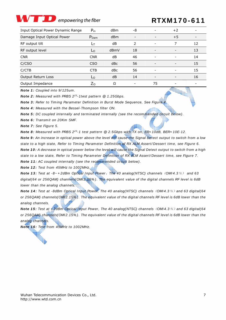
Input Optical Power Dynamic Range Pin dBm -8 - +2 -
Damage Input Optical Power PDam dBm - - +5 -
RF output tilt LT dB 2 - 7 12
RF output level LO dBmV 18 - - 13
CNR CNR dB 46 - - 14
C/CSO CSO dBc 56 - - 15
C/CTB CTB dBc 56 - - 15
Output Return Loss LO dB 14 - - 16
Output Impedance ZO Ω - 75 - -
Note 1: Coupled into 9/125um.
Note 2: Measured with PRBS 223-1test pattern @ 1.25Gbps.
Note 3: Refer to Timing Parameter Definition in Burst Mode Sequence, See Figure 4.
Note 4: Measured with the Bessel-Thompson filter ON.
Note 5: DC coupled internally and terminated internally (see the recommended circuit below).
Note 6: Transmit on 20Km SMF.
Note 7: See Figure 5.
Note 8: Measured with PRBS 223-1 test pattern @ 2.5Gbps with TX on, ER=10dB, BER=10E-12.
Note 9: An increase in optical power above the level will cause the Signal Detect output to switch from a low
state to a high state, Refer to Timing Parameter Definition of RX ALM Assert/Dessert time, see Figure 6.
Note 10: A decrease in optical power below the level will cause the Signal Detect output to switch from a high
state to a low state, Refer to Timing Parameter Definition of RX ALM Assert/Dessert time, see Figure 7.
Note 11: AC coupled internally (see the recommended circuit below).
Note 12: Test from 45MHz to 1002MHz.
Note 13: Test at -8~+2dBm Optical Input Power,The 40 analog(NTSC) channels(OMI4.3%) and 63
digital(64 or 256QAM) channels(OMI2.15%). The equivalent value of the digital channels RF level is 6dB
lower than the analog channels.
Note 14: Test at -8dBm Optical Input Power, The 40 analog(NTSC) channels(OMI4.3%)and 63 digital(64
or 256QAM) channels(OMI2.15%). The equivalent value of the digital channels RF level is 6dB lower than the
analog channels.
Note 15: Test at +2dBm Optical Input Power, The 40 analog(NTSC) channels(OMI4.3%)and 63 digital(64
or 256QAM) channels(OMI2.15%). The equivalent value of the digital channels RF level is 6dB lower than the
analog channels.
Note 16: Test from 45MHz to 1002MHz.

RTXM170-611
Wuhan Telecommunication Devices Co., Ltd.http://www.wtd.com.cn
24
Regulatory ComplianceFeature Test Method Performance
Electrostatic Discharge (ESD)
ImmunityIEC61000-4-2
LV4(Air discharge 15kV,Contact discharge
8kV) Performance criterion B
Electromagnetic Interference(EMI)
CISPR22 ITE Class B
EN55022 Class B
FCC Part15 Class B
Compliant with standards
ImmunityIEC61000-4-3 Class 2
EN55024
Typically show no measurable effect from a
3V/m field swept from 80 to 1000MHz applied
to the transceiver without a chassis enclosure.
Laser Eye Safety
FDA 21 CFR 1040.10
And 1040.11
EN60950
TUV EN60825-1,2
Compliant with Class 1 laser product
RoHS 2002/95/EC 4.1&4.2 Compliant with standards
Ordering Information
Part No.
Specifications
ApplicationPackage
Data rate
BandwidthLaser
Optical
PowerDetector Sensitivity
Video
Detector
AGC
RangeRFcon Top Reach Other
RTXM170-6111×20
SFF
TX:1.25Gb/S
RX1:2.5 Gb/s
RX2:45~1002Mhz
1310nm
DFB
+0.5~
+5dBm
1490nm
APD-TIA
< -28
dBm
1555nm
PIN
-8~
+2dBm3PIN
-40~
85 oC20Km DDM
GPON ONU
Triplexer
Note 1: The length of pigtail is normal 600mm±40mm (the length of connector is included)
Note2 : Min is ambient temperature; max is the module case temperature.
WTD reserves the right to make changes to the product(s) or information contained herein without notice. No
liability is assumed as a result of their use or application. No rights under any patent accompany the sale of
any such product(s) or information.
Edition 2015-12-08
Published by Wuhan Telecommunication Devices Co.,Ltd.
Copyright © WTD
All Rights Reserved.